SD8250中文资料
FR8250 快速使用手册说明书

FR8250 快速使用手册本文档用于对ModbusTCP 适配器和FR 系列IO 模块使用的一个快速说明,阅读背景为具备一定工程经验的人员,旨在让用户能够快速上手。
1. 安装与拆卸1.1. 安装➢对准好下图所示的模块的缺口处;图1-1 对准模块的缺口处➢将IO 模块沿箭头方向推入DIN 卡销,将模块放置在DIN 导轨上;图1-2 将模块安装到导轨上1.2. 拆卸方式➢首先应拆除本模块的所有的信号电缆或电源电缆;➢按箭头方向拉卡销(下图中的黄色部件);➢将模块取下。
图1-3 将模块从导轨上拆卸➢如果遇到有模块难以安装的情况,切勿使用蛮力进行安装,以免损坏当前的模块或其他模块;应当将模块从导轨上拆卸,检查模块是否存在某些异常(比如异物堵塞等),确认没有问题后,再进行插拔。
2. 接线说明本文举例说明以拓扑结构为FR8250 + FR1108 + FR2118 + FR3004 + FR4004 的拓扑结构进行举例说明。
2.1. 端子接线➢ FR 系列IO 模块的接线端子采用了免螺丝设计,安装/拆卸时仅需一把一字型的螺丝刀(推荐使用一字螺丝刀的型号为2 × 75mm)即可。
➢ 推荐使用14AMG 的线,在接线过程中,先将导线剥去一定长度,再用一子型螺丝刀垂直插入端子上的孔内,向下撬动,另一只手将剥去外皮的导线插入已开启的圆形孔内,之后拔出一子型螺丝刀,导线会自动被簧片压紧。
➢ 注意不要将电源的正负极接反,否则有可能会导致模块无法工作、工作异常,甚至会导致模块损毁。
2.2. 电源接线➢如下图所示,使用一块220V-24V 的电源模块(最好是双路输出的),将电源线接好:图2-1 连接FR8250 的系统电源2.3. 系统公共端电源接线➢如下图2-2 所示,再将系统的公共端电源接好:注意:适配器的系统与现场测电压是通过总站和总线电源模块提供的。
适配器现场测组件是没有内部过电流保护,因此,对于这类的组件电源,必须在外部添加适当的过电流保护器件来实现过流生产,例如通过外加5A的保险丝。
第十九讲 可编程接口芯片及应用(8250A)(2)
第八章 可编程接口芯片及应用技术
4)具有独立的接收时钟输入引脚。 )具有独立的接收时钟输入引脚。 5)有CPU发向调制解调器的信号,还有能接收 ) 发向调制解调器的信号, 发向调制解调器的信号 并记录由调制解调器发送到计算机的状态信息。 并记录由调制解调器发送到计算机的状态信息 。 可方便地与MODEM相连。 相连。 可方便地与 相连 6)具有带优先级排序的中断系统,有多种中断 )具有带优先级排序的中断系统, 源。 7)具有可记录所有状态信息的状态寄存器和检 ) 查起始位出错的能力。 查起始位出错的能力。
图 6 33 传 输 线 控 制 寄 存 器 LCR LCR
的 0= 1= 0= 1= 00=5 01=6 10=7 11=8 1 (D4=1,D3=1, 0 , 0=1 1= 6~8 SOUT 2 的 5 1.5
的 控 制 字 格
, D4=0,D3=1, 1) 0= 1=
(DLAB) 0= RBR TBR IER 1= 存器 DLL DLH
第八章 可编程接口芯片及应用技术
第十九讲 7.3 可编程串行输入 输出接口芯片 可编程串行输入/输出接口芯片 输出接口芯片8250A
7.3.2 Intel 8250A
返回本章首页
第八章 可编程接口芯片及应用技术
7.3.2 Intel 8250A
1.主要功能 . INS 8250的主要功能有: 的主要功能有: 的主要功能有 1)8250支持异步通信规程。 ) 支持异步通信规程。 支持异步通信规程 2)8250的异步通信的数据格式可由 ) 的异步通信的数据格式可由 用户编程选择。 用户编程选择。 3)内部具有可编程时钟产生电路。 )内部具有可编程时钟产生电路。
AL,0EH ;7位字符,1位停止位,奇校验 , 位字符, 位停止位 位停止位, 位字符 DX,AL ;写入 , 写入LCR控制字 控制字 DX,2FCH , AL,03H , DX,AL , DX,2F9H ;设定 , 设定IER口地址 口地址 ;禁止一切中断 ;设定MCR口地址 设定 口地址 ;置MCR控制字 控制字
a7 8250串口

线路控制寄存器(LCR):
LCR用来设定通讯所需的一些基本参数。Bit7为1指定波特率因子寄 存器有效,为0则指定发送/接收及IER有效。Bit6置1会将发送端置为 0,这将会使接收端产生一个“间断”。Bit3-5用来设定是否使用奇偶
线路控制寄存器(LCR):
校验以及奇偶校验的类型,Bit3=1时使用校验,Bit4为0则为奇校验, 1为偶校验,而Bit5则强制校验为1或0,并由Bit4决定具体为0或1。 Bit2用来设定停止位的长度,0表示1位停止位,为1则根据数据长度 的不同使用1.5-2位停止位。Bit0:1用来设定数据长度。
程序清单
ORG 39A0 PDATA EQU 8000H MSB EQU 8001H LINE EQU 8003H LSTAT EQU 8005H START:MOV SP,#50H;堆栈指针初始化 MOV A,#80H ;(A)=1000 0000B MOV DPTR, #LINE;通讯线控制寄存器地址送DPTR MOVX @DPTR, A;第七位为1,设置波特率 MOV A,#18H ;波特率为4800时的低8位值为18H MOV DPTR, #8000H; 由于DLAB=1,所以此时8000H为设置低8位波 ;特率地址 MOVX @DPTR , A;高波特率的低8位数据为18H MOV DPTR , #MSB;8001H送DPTR,送波特率的高8位地址给DPTR MOV A, #00H;波特率高8位数据为00H MOVX @DPTR ,A ;设波特率高8位数据为00H MOV A,#03H ;(A)=0000 0011B MOV DPTR,#LINE ; MOVX @DPTR, A ;字符码长充为8位,1位停止位 MOV A,#00H ;(A)=0000 0000B
MB85502-015资料
436 mW max. (ADD=L)
• LVTTL compatible I/O • Programmable burst type • Programmable burst length • Auto and Self-refresh • CKE power down mode • Output Enable and Input Data Mask
CLK A0 to A11 RAS
DQM
CKE
4M × 4
CS
chip 1
CAS WE
DQ DQ DQ DQ
CLK A0 to A11 RAS
DQM
CKE
4M × 4
CS
chip 2
CAS WE
DQ DQ DQ DQ
CLK A0 to A11 RAS
DQM
CKE
4M × 4
CS
chip 3
CAS WE
s ABSOLUTE MAXIMUM RATINGS (See NOTE)
Parameter Supply Voltage Input Voltage Output Voltage Short Circuit Output Current Power Dissipation Storage Temperature *1 VSS = 0 V
Ambient Oprating
Temp. 0°C to +70 °C
s CAPACITANCE
Parameter Input Capacitance, A0 to A11 Input Capacitance, RAS, CAS, WE Input Capacitance, CLK Input Capacitance, DQM0, DQM1 Input Capacitance, CKE0, CKE1 Input Capacitance, CS0, CS1 I/O Capacitance, (DQ0 to DQ35)
ARMCortexA8构架介绍.
ARM Cortex A8不是CPU,是个内核,只是构架。
一般TI德州仪器,三星会炫耀其CPU 是A8构架,我不清楚楼主说的是哪款。
如果同主频的高通与TI或三星比,高通数据处理最快,系统运行和上网速度优于三星与TI,但图形处理不如三星与TI。
如果不是同主频,1GBhz高通,比TI或三星的600MBhz,那高通的系统运行速度是其两款的两倍以上,由于主频不同,TI或三星,的图形处理优势也全无。
目前市面上的CPU大体分为三大厂商,高通,TI德州仪器,三星。
三个厂商都是买ARM 执照在改造ARM构造。
高通与TI,三星不同,高通是把A8做为平台,工艺技术跟A8接近,而TI与三星是改造A8为自己所用。
我把主频定为1GBhz,来对比。
1.高通:高通的Snapdragon SD8X50是最早与大家见面的1GHz处理器解决方案,基于Cortex-A8架构,它集中于CPU,GPU ,通信芯片,GPS芯片等多种芯片,很多厂商喜欢高通的CPU,原因是1个高通CPU,通信、GPS…全部解决很省地。
该图形处理器基本数据为输出为22Mpolygon/sec,像素填充率为1.33亿。
它GPU的图形处理能力是这三个厂里最弱的。
但高通的Snapdragon处理器在数据处理能力上要略高于其他Cortex-A8的处理器,所以Snapdragon SD8250在系统运行及数据运算上还是略优于其他处理器。
它的Radio最好最适合手机,系统运行快,上网快,不足多媒体比其他两厂要差,多媒体是指图形处理能力也就是玩游戏之类的,采用较大的65MN,耗电大。
HTC最爱,代表作HTC Desire G7。
2.TI德州仪器:德州仪器OMAP36xx系列处理器也是基于Cortex-A8架构的解决方案。
该图形处理器基本数据为多边形生成率为14Mpolygon/sec,象素填充率为每秒5亿,它是这三个厂商的CPU 中数据处理最弱的,但多媒体能力强于高通,45MN更省电?Moto 最爱,代表作Moto Droid2。
SD25-820中文资料
Description• Six sizes of shielded drum core inductors with low profiles (as low as 1.0mm) and high power density • Inductance range from .47uH to 1000uH• Current range from 6.00 to 0.088 Amps• Ferrite shielded, low EMIApplications• Digital cameras, CD players, cellular phones, and PDAs • PCMCIA cards• GPS systemsEnvironmental Data• Storage temperature range:-40C to +125C• Operating ambient temperature range:-40C to +85C (range is application specific).T emperature rise is approximately 40C at rated rms current• Infrared reflow temperature:+240C for 30 seconds maximum Packaging• Supplied in tape and reel packaging, 3800 (SD10, SD12 and SD18), 2900 (SD20 and SD25), and 3500 (SD52)per reelSD SeriesHigh Power Density,Low Profile,Shielded Inductors(1) Open Circuit Inductance T est Parameters:100KHz, 0.25Vrms, 0.0Adc.(2) RMS current for an approximate ∆T of 40°C without core loss.It isrecommended that the temperature of the part not exceed 125°C. (3) Peak current for approximate 30% roll off at 20°C.(4) DCR limits @ 20°C.5) Applied Volt-Time product (V-uS) across the inductor at 100kHz necessary togenerate a core loss equal to 10% of the total losses for 40°C temperature rise.Part Number Rated OCL (1)Part Irms (2)Isat (3)DCR (4)Volt Inductance+/-20%Marking Amperes Amperes(Ω)u-sec (µH)(µH)Typ.Typ. SD10-R470.4700.453A 2.59 3.540.0249 2.1 SD10-1R0 1.00 1.119B 1.93 2.250.0448 3.3 SD10-1R5 1.50 1.563C 1.60 1.910.0653 3.9SD10-4R7 4.70 4.893F 1.04 1.080.1535 6.9 SD10-6R2 6.20 6.743G0.940.920.18708.1 SD10-8R28.208.889H0.8000.8000.26079.3 SD10-10010.010.07J0.7600.7520.28889.9 SD10-15015.015.55K0.6130.6050.442912.3 SD10-22022.022.21L0.4980.5060.671814.7 SD10-33033.032.20M0.4120.4200.980717.7SD10-68068.070.01O0.3010.285 1.8426.1 SD10-82082.083.48P0.2580.261 2.5028.5 SD10-101100102.0Q0.2250.236 3.2931.5 SD10-151150149.2R0.2000.195 4.1538.1 SD10-221220222.2S0.1610.160 6.4146.5 SD10-331330330.4T0.1300.1319.8356.7 SD10-471470468.3U0.1170.11012.1067.5 SD12-R470.4700.490A 3.19 3.860.0246 2.84 SD12-1R2 1.20 1.21B 2.62 2.450.0366 4.47 SD12-1R5 1.50 1.69C 2.19 2.080.0521 5.28 SD12-2R2 2.20 2.25D 1.83 1.800.0747 6.09 SD12-3R3 3.30 3.61E 1.55 1.420.10437.71 SD12-4R7 4.70 4.41F 1.46 1.290.11778.53 SD12-6R2 6.20 6.25G 1.21 1.080.169910.15 SD12-8R28.208.41H 1.020.9310.239911.77SD12-22022.022.09L0.6280.5740.633819.08 SD12-33033.032.49M0.5190.4740.928923.14 SD12-47047.047.61N0.4280.391 1.3728.01 SD12-68068.068.89O0.3410.325 2.1633.70 SD12-82082.082.81P0.3260.297 2.3636.95 SD12-10110098.0Q0.3080.273 2.6440.19 SD12-151150151.3R0.2510.220 3.9649.94(1) Open Circuit Inductance T est Parameters:100KHz, 0.25Vrms, 0.0Adc.(2) RMS current for an approximate ∆T of 40°C without core loss.It is recommended that the temperature of the part not exceed 125°C.(3) Peak current for approximate 30% roll off at 20°C.(4) DCR limits @ 20°C.5) Applied Volt-Time product (V-uS) across the inductor at 100kHz necessary to generate a core loss equal to 10% of the total losses for 40°C temperature rise.Part Number Rated OCL (1)Part Irms (2)Isat (3)DCR (4)Volt Inductance+/-20%Marking Amperes Amperes (Ω)u-sec (µH)(µH)Typ.Typ.SD12-331330334.9T 0.1860.1487.2574.30SD12-471470462.3U 0.1670.1268.9587.29SD12-681680670.8V 0.1490.10411.30105SD12-821820800.9W 0.1290.09514.93115SD12-1021000992.3X 0.1210.08617.20128SD18-R470.470.49A 3.58 4.630.0201 2.35SD18-R820.820.81B 3.24 3.600.0247 3.02SD18-1R5 1.50 1.69D 2.73 2.490.0345 4.37SD18-2R2 2.20 2.25E 2.55 2.160.0398 5.04SD18-3R3 3.30 3.61F 2.07 1.710.0605 6.38SD18-4R7 4.70 4.41G 1.77 1.540.08247.06SD18-6R2 6.20 6.25H 1.61 1.300.10008.40SD18-8R28.208.41J 1.38 1.120.13519.74SD18-10010.010.89K 1.280.9820.158411.09SD18-22022.022.09M 0.8760.6890.336615.79SD18-33033.032.49N 0.7150.5680.505719.15SD18-47047.047.61O 0.5780.4700.773223.18SD18-68068.068.89P 0.5140.3900.979827.89SD18-82082.082.81Q 0.4460.356 1.3030.58SD18-101100102.01R 0.4190.321 1.4733.94SD18-151150151.29S 0.3450.263 2.1841.33SD18-221220222.01T 0.2960.217 2.9550.06SD18-471470479.61V 0.2010.148 6.3973.58SD18-681680681.21W 0.1670.1249.2887.70SD18-821820823.69X 0.1450.11312.3596.43SD18-10210001004Y 0.1360.10214.01107SD20-R470.470.490A 3.59 4.000.0200 2.28SD20-1R2 1.20 1.21B 3.07 2.550.0275 3.58SD20-1R5 1.50 1.69C 2.88 2.150.0312 4.23SD20-3R3 3.30 3.61E 2.17 1.470.0547 6.18SD20-4R7 4.70 4.41F 2.05 1.330.0612 6.83SD20-6R2 6.20 6.25G 1.89 1.120.07208.13SD20-8R28.208.41H 1.610.9660.10009.43SD20-10010.09.61J 1.530.9030.110010.08SD20-15015.015.21K 1.250.7180.165512.68SD20-22022.022.09L 1.120.5960.205315.28SD20-47047.047.61N 0.7450.4060.465022.43SD20-68068.068.89O 0.6100.3370.694726.98SD20-82082.082.81P 0.5760.3080.778529.58SD20-10110098.01Q 0.4950.283 1.0632.18SD20-151150151.3R 0.4350.228 1.3739.98SD20-221220222.0S 0.3560.188 2.0448.43SD20-331330327.6T 0.2940.155 2.9958.83SD20-471470470.9U 0.2630.129 3.7470.53SD20-821820823.7W 0.2040.098 6.2293.28SD20-10210001004.9X 0.1720.0888.73103SD25-R470.470.466A 3.88 6.000.0177 2.13SD25-R820.820.770B 3.58 4.670.0208 2.74SD25-1R2 1.20 1.15C 3.33 3.810.0240 3.34SD25-1R5 1.50 1.61D 3.12 3.230.0274 3.95SD25-2R22.202.14E2.932.800.03114.56SD SeriesHigh Power Density,Low Profile,Shielded InductorsMechanical Diagrams TOP VIEWBOTTOM VIEWRECOMMENDED PCB LAYOUTSCHEMATIC215.2Max5.2Max aHT1.5 Typ.Ref.12SIDE VIEWPin #1identifierPart marking(Note A)21R2.2502.9755.9502.97524 PAD LAYOUTR2.2505.9591.02.97525.152.57522 PAD LAYOUT5.9509(see chart below)Part Number Rated OCL (1)Part Irms (2)Isat (3)DCR (4)Volt Inductance+/-20%Marking Amperes Amperes (Ω)u-sec (µH)(µH)Typ.Typ.SD25-3R3 3.30 3.43F 2.64 2.210.0384 5.78SD25-4R7 4.70 5.03G 2.39 1.830.0467 6.99SD25-6R8 6.80 6.93H 2.19 1.560.05568.21SD25-8R28.207.99J 1.92 1.450.07248.82SD25-10010.010.35K 1.80 1.270.082410.03SD25-15015.014.45L 1.67 1.080.095611.86SD25-22022.022.81M 1.340.8570.147814.90SD25-33033.033.07N 1.110.7110.214917.94SD25-47047.047.89O 0.9190.5920.315621.58SD25-68068.068.64P 0.7410.4820.485025.84SD25-82082.082.17Q 0.7130.4410.524228.27SD25-101100100.79R 0.6700.3980.593731.31SD25-151150148.4S 0.5530.3280.872338.00SD25-221220222.4T 0.4460.268 1.3446.51SD25-331330332.2U 0.3590.219 2.0756.85SD25-471470472.4V 0.2930.184 3.1067.79SD25-681680677.2W 0.2620.154 3.8881.17SD25-821820826.7X 0.2300.139 5.0489.68SD25-10210001003.4Y0.2160.1265.7098.80Series HT SD10 1.0mm max SD12 1.2mm max SD18 1.8mm max SD20 2.0mm max SD25 2.5mm max(1) Open Circuit Inductance T est Parameters:100KHz, 0.25Vrms, 0.0Adc.(2) RMS current for an approximate ∆T of 40°C without core loss.It is recommended that the temperature of the part not exceed 125°C.(3) Peak current for approximate 30% roll off at 20°C.(4) DCR limits @ 20°C.5) Applied Volt-Time product (V-uS) across the inductor at 100kHz necessary to generate a core loss equal to 10% of the total losses for 40°C temperature rise.SD SeriesHigh Power Density,Low Profile,Shielded InductorsSD SeriesA) Part Marking:Line 1:(1st digit indicates the inductance value per part marking designator in chart above)(2nd digit is a bi-weekly production date code)(3rd digit is the last digit of the year produced)Line 2:12 (indicates the product size code)Direction of feedSECTION A-ASD20/25 SeriesDimensions are in millimeters.Direction of feedSD12/18 SeriesPackaging Information ACTUAL SIZESD12ACTUAL SIZESD18ACTUAL SIZESD20ACTUAL SIZESD25SD SeriesHigh Power Density,Low Profile,Shielded InductorsAo=5.45mm Bo=5.45mm Ko=2.00mmParts packaged on 13" Diameter reel, 3,800 parts per reel.Direction of feedSECTION A-ASD10 SeriesACTUAL SIZESD10Ao=5.45mm Bo=5.45mm Ko=1.20mmParts packaged on 13" Diameter reel,3,800 parts per reel.Ao=5.45mm Bo=5.45mm Ko=2.70mmParts packaged on 13" Diameter reel,2,900 parts per reel.SD SeriesHigh Power Density,Low Profile,Shielded InductorsDC Current vs.TemperatureIdc (A)T e m p e r a t u r e R i s e (D e g . C)0.000.100.200.300.400.500.600.70Idc (A)T e m p e r a t u r e R i s e (D e g . C )SD10-220Idc (A)T e m p e r a t u r e R i s e (D e g . C)SD10-471Idc (A)T e m p e r a t ur e R i s e (D e g . C )T e m p e r a t u r e R i s e (D e g . C )0.000.100.200.300.400.500.600.700.80Idc (A)T e m p e r a t u r e R i s e (D e g . C )Idc (A)T e m p e r a t u r e R i s e (D e g . C )Idc (A)T e m p e r a t u r e R i s e (D e g . C )Idc (A)T e m p e r a t u r e R i s e (D e g . C )Idc (A)T e m p e r a t u r e R i s e (D e g . C )RolloffCore LossOCL vs Isat SD100102030405060708090100% of Isat O C L (%)OCL vs Isat SD1201020304050607080901000102030405060708090100110120% of Isat O C L (%)OCL vs Isat SD1801020304050607080901000102030405060708090100110120130140150160% of IsatO C L (%)OCL vs Isat SD2001020304050607080901000102030405060708090100110120130140150160170% of IsatO C L (%)OCL vs Isat SD2501020304050607080901000102030405060708090100110120130140150% of IsatO C L (%)Irms DERATING WITH CORE LOSS% of Applied Volt-µSecond% o f L o s s e s f r o m I r m s (m a x i m u m)SD SeriesHigh Power Density,Low Profile,Shielded InductorsSD SeriesHigh Power Density,Low Profile,Shielded InductorsPart Number Rated OCL (1)Part Irms (2)Isat (3)DCR (4)Volt Inductance+/-20%Marking Amperes Amperes (Ω)u-sec (µH)(µH)Typ.Typ.SD52-1R2 1.20 1.20A 2.33 3.140.0279 1.49SD52-2R2 2.20 2.20B 1.98 2.300.0385 2.03SD52-3R5 3.50 3.50C 1.73 1.820.0503 2.57SD52-4R7 4.70 4.70D 1.63 1.640.0568 2.84SD52-6R8 6.80 6.80E 1.39 1.280.0777 3.65SD52-10010.010.0F 1.11 1.110.1215 4.19SD52-15015.015.0G 0.970.880.1618 5.27SD52-22022.022.0H 0.860.730.2042 6.35SD52-27027.027.0J 0.730.650.28647.16SD52-33033.033.0K 0.700.610.30747.70SD52-47047.047.0L 0.580.500.44659.32SD52-68068.068.0M 0.470.420.682911.21SD52-101100100N0.390.351.000013.37RECOMMENDED PCB LAYOUTSCHEMATIC2.02 plcs6.01.32 plcsBOTTOM VIEW1SIDE VIEW±SD52 SeriesA) Part Marking:Line 1:(1st digit indicates the inductance value per part markingdesignator in chart above)(2nd digit is a bi-weekly production date code)(3rd digit is the last digit of the year produced)Line 2:12 (indicates the product size code)Mechanical Diagrams Dimensions are in millimeters.Direction of feedKoSECTION A-A1.5 Dia min.BoB AoA 8.0804.002.00± 0.051.5 Dia.+0.1/-0.0AA1.755.5012.0+/-0.30210.203.0SD52 SeriesACTUAL SIZESD52Ao=5.72mm Bo=5.72mm Ko=2.30mmParts packaged on 13" Diameter reel,3,500 parts per reel.(1) Open Circuit Inductance T est Parameters:100KHz, 0.25Vrms, 0.0Adc.(2) RMS current for an approximate ∆T of 40°C without core loss.It is recommended that the temperature of the part not exceed 125°C.(3) Peak current for approximate 30% roll off at 20°C.(4) DCR limits @ 20°C.5) Applied Volt-Time product (V-uS) across the inductor at 100kHz necessary to generate a core loss equal to 10% of the total losses for 40°C temperature rise.Packaging InformationSD SeriesHigh Power Density,Low Profile,Shielded InductorsOCL vs Isat SD5201020304050607080901000102030405060708090100110120130140% of IsatO C L (%)RolloffDC Current vs.TemperatureIdc (A)T e m p e r a t u r e R i s e (D e g . C)0.00.5 1.0 1.5 2.0 2.5 3.0 3.5 4.0Idc (A)T e m p e r a t u r e R i s e (D e g . C )Visit us on the Web at 3601 Quantum Boulevard Boynton Beach, Florida 33426-8638T el:+1-561-752-5000 T oll Free:+1-888-414-2645 Fax:+1-561-742-1178This bulletin is intended to present product design solutions and technical information that will help the end user with design applications. Cooper Electronic Technologies reserves the right, without notice, to change design or construction of any products and to discontinue or limit distribution of any products. Cooper Electronic Technologies also reserves the right to change or update, without notice, any technical information contained in this bulletin. Once a product has been selected, it should be tested by the user in all possible applications.PM-4311 1/03© Cooper Electronic Technologies 2003。
硬件8250介绍

0 数字信号
1
1
0
1
0
0
0
1
(a)调幅
按数字信号的 值改变载波信 号的幅度 按数字信号的 值改变载波信 号的频率 按数字信号的 值改变载波信 号的相位
(b)调频
(c)调相
7.4.2 串行通信接口标准
一、EIA RS-232C/CCITT V.24标准 • EIA RS—232C,1969年,适合于DTE和 DCE之间相互连接与通信的串行通信规程。 (1987年11月,经修改正式命名为RS— 232D) DTE-Data Terminal Equipment DCE-Data Communication Equipment。
CCITT 信号名
插 脚 号 1
机壳地
101
103 104
发送数据
2 3 接收数据
载波检测
105 终 4 106 5
请求发送
允许发送 Modem就绪
本 地 Modem
远 程 Modem
计 算 机
107 端 6
信号地 102
109 108 125 7 8 20 22 载波检测 终端就绪
电话线
பைடு நூலகம்
呼叫指示
7.4 串行通信及8250接口芯片
•通信概念 数据在单条1位宽的传输线上按时间先 后一位一位地传送;节省传输线(优点); 数据传输率较低(缺点)。 主要适用于长距离、低速率的通信中。 •常用物理标准(RS-232) •8250通信控制器
基本概念
1. 通信方式
– – – – 串行与并行 单工、半双工、全双工 异步通信的字符编码 同步与异步通信
• 例:SDLC/HDLC帧格式: • 假定数据长度为2048位, 通信效率为:2048/(2048+48)=97% 协议开销仅为3% • 一般公式:SDLC/HDLC协议开销=1.0- N/(N+48),其中N为发送数据的比特数。
AD8250_datasheet
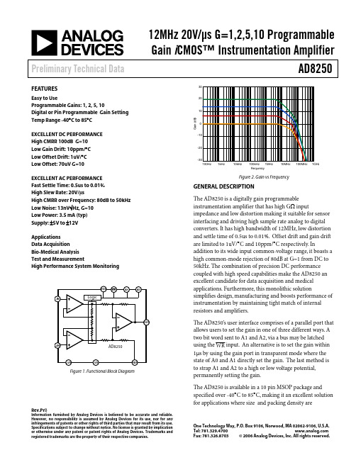
12MHz 20V/μs G=1,2,5,10 Programmable Gain i CMOS™ Instrumentation AmplifierPreliminary Technical DataAD8250Rev.Pr BInformation furnished by Analog Devices is believed to be accurate and reliable. However, no responsibility is assumed by Analog Devices for its use, nor for any infringements of patents or other rights of third parties that may result from its use. Specifications subject to change without notice. No license is granted by implication or otherwise under any patent or patent rights of Analog Devices. Trademarks and registered trademarks are the property of their respective companies.One Technology Way, P.O. Box 9106, Norwood, MA 02062-9106, U.S.A.Tel: 781.329.4700 Fax: 781.326.8703© 2006 Analog Devices, Inc. All rights reserved.FEATURESEasy to UseProgrammable Gains: 1, 2, 5, 10Digital or Pin Programmable Gain Setting Temp Range -40°C to 85°CEXCELLENT DC PERFORMANCE High CMRR 100dB G=10 Low Gain Drift: 10ppm/°C Low Offset Drift: 1uV/°C Low Offset: 70uV G=10EXCELLENT AC PERFORMANCE Fast Settle Time: 0.5us to 0.01% High Slew Rate: 20V/μsHigh CMRR over Frequency: 80dB to 50kHz Low Noise: 13nV √Hz, G=10 Low Power: 3.5 mA (typ) Supply: ±5V to ±12VApplications Data Acquisition Bio-Medical Analysis Test and MeasurementHigh Performance System MonitoringFigure 1. Functional Block Diagram100MHz10MHz1MHz 100kHz10kHz1kHz100HzG a i n (d B )F requencyFigure 2. Gain vs FrequencyGENERAL DESCRIPTIONThe AD8250 is a digitally gain programmable instrumentation amplifier that has high G Ω inputimpedance and low distortion making it suitable for sensor interfacing and driving high sample rate analog to digital converters. It has high bandwidth of 12MHz, low distortion and settle time of 0.5us to 0.01%. Offset drift and gain drift are limited to 1uV/°C and 10ppm/°C respectively. Inaddition to its wide input common-voltage range, it boasts a high common-mode rejection of 80dB at G=1 from DC to 50kHz. The combination of precision DC performance coupled with high speed capabilities make the AD8250 an excellent candidate for data acquisition and medical applications. Furthermore, this monolithic solutionsimplifies design, manufacturing and boosts performance of instrumentation by maintaining tight match of internal resistors and amplifiers.The AD8250’s user interface comprises of a parallel port that allows users to set the gain in one of three different ways. A two bit word sent to A1 and A2, via a bus may be latched using the WR input. An alternative is to set the gain within 1μs by using the gain port in transparent mode where the state of A0 and A1 directly set the gain. The last method is to strap A1 and A2 to a high or low voltage potential, permanently setting the gain.The AD8250 is available in a 10 pin MSOP package and specified over -40°C to 85°C, making it an excellent solution for applications where size and packing density areAD8250Preliminary Technical DataRev. PrB | Page 2 of 8important considerations.TABLE OF CONTENTSAD8250—Specifications..................................................................3 Timing Diagram...........................................................................5 Absolute Maximum Ratings............................................................6 Pin Configurations And Functional Descriptions.......................7 Transparent Gain Setting Mode:.................................................7 Write Enable Gain Setting Mode:................................................7 Outline Dimensions..........................................................................8 ESD Caution.. (8)REVISION HISTORYPreliminary Revision : BPreliminary Technical DataAD8250Rev. PrB| Page 3 of 8AD8250—SPECIFICATIONSTable 1. V S = ±12 V, V REF = 0 V (@T A = 25o C, G = +1, R L = 2 kΩ, unless otherwise noted.)AD8250ARM Parameter Conditions Min Typ Max Unit COMMON-MODE REJECTION RATIO(CMRR)CMRR to 60 Hz with 1 k Ω SourceImbalanceV CM = -10 V to +10 V G = 1 80 dB G = 2 86 dB G = 5 94 dBG = 10 100 dB CMRR to 50kHz V CM = -10 V to +10 VG = 1 80 dB G = 2 dB G = 5 dB G = 10 dBNOISE Voltage Noise, 1kHz G=1 32 nV/√Hz G=2 20 nV/√Hz G=5 14 nV/√Hz G=10 13 nV/√Hz RTI, 0.1 Hz to 10 Hz G=1 μV p-p G=2 μV p-p G=5 μV p-p G=10 μV p-p Current Noise f = 1kHz fA/√Hz VOLTAGE OFFSETOffset, V OS G=1, V S = ±5 V to ±12 V 250 μVOver Temperature T = -40°C to +85°C μVAverage TC T = -40°C to +85°C μV/°COffset, V OS G=2, V S = ±5 V to ±12 V 150 μVOver Temperature T = -40°C to +85°C μVAverage TC T = -40°C to +85°C μV/°COffset, V OS G=5, V S = ±5 V to ±12 V 90 μVOver Temperature T = -40°C to +85°C μVAverage TC T = -40°C to +85°C μV/°COffset, V OS G=10, V S = ±5 V to ±12 V 70 μVOver Temperature T = -40°C to +85°C μVAverage TC T = -40°C to +85°C μV/°COffset Referred to the Input vs.Supply (PSR) V S = ±8 V to ±12 VG = 1 115 dB G = 2 110 dB G = 5 110 dB G = 10 96 110 dBINPUT CURRENT Input Bias Current 10 25 nA Over Temperature T = -40°C to +85°C35 nAAD8250 Preliminary Technical DataRev. PrB | Page 4 of 8 AD8250ARMParameter Conditions Min Typ Max Unit Average TC pA/°CInput Offset Current 5 10 nA Over Temperature T = -40°C to +85°C nAAverage TC 1.5 pA/°CDYNAMIC RESPONSESmall Signal -3dB BandwidthG=1 17 MHzG=2 15 MHzG=5 10 MHzG=10 3.5 MHz Settling Time 0.01% 10 V StepG=1 0.5 μSG=2 μSG=5 μSG=10 μS Settling Time 0.001% 10 V StepG=1 1.5μS G=2 μSG=5 μSG=10 μSSlew RateG=1 20 35 V/μS G=2 3035V/μS G=5 3035V/μSG=10 3035V/μSTotal Harmonic Distortion +Noise RL = 100kOhms, G=1 %RL = 2kOhms, G=1 %GAINGain Range: 1, 2, 5, 10 1 10 V/VGain Error V OUT= ±10 VG=1 0.05% G=2G=5G=10Gain Nonlinearity V OUT = –10 V to +10 VG=1,R L = 10 kΩ 4ppm G=2,R L = 10 kΩ 4ppm G=5,R L = 10 kΩ 4ppm G=10,R L = 10 kΩ 4ppm Gain Nonlinearity G=1-10, R L = 2 kΩ 4ppm Gain vs. Temperature All Gains 10 ppm/°CINPUTInput ImpedanceDifferential 1|| 2 GΩ|| pFCommon Mode 1|| 2 GΩ|| pFInput Operating Voltage Range V S = ±5 V to ±12 V -Vs + 1 +Vs 1.5 VOver Temperature T = -40°C to +85°CVPreliminary Technical DataAD8250Rev. PrB| Page 5 of 8AD8250ARMParameter Conditions Min Typ Max UnitOUTPUT R L = 10 k Ω, Output Swing V S = ±5 V to ±12 V –Vs + 1.5 +Vs –1.5 VOver Temperature T = -40°C to +85°C V Short Circuit Current 20 mA REFERENCE INPUTR IN 20 k Ω I IN V IN +, V IN –, V REF = 0 μAVoltage Range –Vs +Vs V Gain to Output V/V Digital Logic Inputs V Digital Ground Voltage, DGND V Digital Input Voltage Low Referenced to DGND 1 V Digital Input Voltage High Referenced to DGND 4 V Digital Input Leakage Current pA Gain Switching Time ns T SU nsT HD ns T WR_LO ns T WR_HI nsPOWER SUPPLYOperating Range 3 ±5 ±12Quiescent Current 3.5 mA Over Temperature T = -40°C to +85°C mA TEMPERATURE RANGE Specified Performance –40 +85 °CTIMING DIAGRAMWRA0, A1Figure 3.Timing DiagramAD8250Preliminary Technical DataRev. PrB | Page 6 of 8ABSOLUTE MAXIMUM RATINGSTable 2. AD8250 Absolute Maximum RatingsParameter Rating Supply Voltage +/-14V Power Dissipation See Figure 2 Output Short Circuit Current Common-Mode Input Voltage -Vs – 0.5 V to +Vs + 0.5 V Differential Input Voltage V Storage Temperature –65°C to +125°C Operating Temperature Range –40°C to +85°CLead Temperature Range(Soldering 10 sec) °C Junction Temperature °CΘJA (4 layer JEDEC Standard°C/W Board)Package Glass Transition Temperature°C ESD (Human Body Model) kV ESD (Charge Device Model) kV ESD (Machine Model)kVStresses above those listed under Absolute Maximum Ratingsmay cause permanent damage to the device. This is a stress rating only and functional operation of the device at these or any other condition s above those indicated in the operational section of this specification is not implied. Exposure to absolute maximum rating conditions for extended periods may affect device reliability.Preliminary Technical DataAD8250Rev. PrB| Page 7 of 8PIN CONFIGURATIONS AND FUNCTIONAL DESCRIPTIONS-IN DGND -VS A0A1+INVREF+VS VOUT WRFigure 4. 10-Lead MSOPTable 3. Pin Function Descriptions—GAIN SETTINGThe AD8250’s gains are set digitally. The A0 and A1 pins must be set either HIGH or LOW with respect to digital ground,DGND. The WR pin is a tri-state switch. It may be set to one of three levels, HIGH, LOW or to –VS. A HIGH signal is typically greater than 4V but less than 6V and a LOW signal is typically less than 1V but higher than DGND, 0V. Gains can be programmed using the following methods:TRANSPARENT GAIN SETTING MODE:In this mode, the gain is set by toggling A0 and A1 to HIGH or LOW . To enable transparent mode, tie WR to –Vs. Thisconfigures the AD8250 to change gains when A0 and A1 are set according to Table 4.WRITE ENABLE GAIN SETTING MODE:In this mode, the gains are changed only during the negativeedge of the WR strobe. So for instance, the gain is determined by the two bit value held on A0 and A1 at the time the WR strobe transitions from HIGH to LOW .WRA0, A1X = don’t care.AD8250Preliminary Technical DataRev. PrB | Page 8 of 8OUTLINE DIMENSIONSCOMPLIANT TO JEDEC STANDARDS MO-187-BACOPLANARITY0.10Figure 5. 10 Lead MSOP (RM) – Dimensions shown in millimetersESD CAUTIONESD (electrostatic discharge) sensitive device. Electrostatic charges as high as 4000 V readily accumulate on the human body and test equipment and can discharge without detection. Although this product features proprietary ESD protection circuitry, permanent damage may occur on devices subjected to high energy electrostatic discharges. Therefore, proper ESD precautions are recommended to avoid performance degradation or loss of functionality.Table 6. Ordering GuideAD00000 Products Temperature Package Package DescriptionPackage OptionBranding AD8250ARZ –40°C to +85°C 10-Lead MSOP RM-10 AD8250ARZ-RL –40°C to +85°C 10-Lead MSOP RM-10 AD8250ARZ-R7 –40°C to +85°C 10-Lead MSOPRM-10AD8250-EVA LEvaluation BoardP R 06288-0-8/06(P r B )。
RT8250资料
Functional Pin DescriptionTypical Application CircuitOUT 3.3V/3A VElectrical Characteristics(V = 12V, T = 25°C unless otherwise specified)Note 1. Stresses listed as the above "Absolute Maximum Ratings"may cause permanent damage to the device. These are for stress ratings. Functional operation of the device at these or any other conditions beyond those indicated in the operational sections of the specifications is not implied. Exposure to absolute maximum rating conditions for extended periods may remain possibility to affect device reliability.Note 2. θJA is measured in the natural convection at T A = 25°C on a high effective thermal conductivity four-layer test board of JEDEC 51-7 thermal measurement standard. The case position ofθJC is on the exposed pad of the package.Note 3. Devices are ESD sensitive. Handling precaution is recommended.Note 4. The device is not guaranteed to function outside its operating conditions.Current Limit vs. Duty Cycle3.03.54.04.55.05.56.06.57.00102030405060708090100Duty Cycle (%)C u r r e n t L i m i t (A)Current Limit vs. Temperature3.03.54.04.55.05.56.06.57.0-50-25255075100125Temperature C u r r e n t L i m i t (A)(°C)SwitchingTime (1μs/Div)V IN = 12V, V OUT = 3.3V, I OUT = 3AV OUT (10mV/Div)V SW (10V/Div)I L (2A/Div)Power On from V INTime (5ms/Div)V IN (5V/Div)V OUT (2V/Div)I L (2A/Div)V IN = 12V, V OUT = 3.3V, I OUT = 3APower Off from ENTime (1ms/Div)V IN = 12V, V OUT = 3.3V, I OUT = 3AV EN (5V/Div)V OUT (2V/Div)I OUT (2A/Div)Power On from EN Time (5ms/Div)V EN (5V/Div)V OUT (2V/Div)I OUT (2A/Div)V IN = 12V, V OUT = 3.3V, I OUT = 3A(200mV/Div)(2A/Div)V IN = 12V, V OUT = 3.3V, I OUT = 0A to 1.5AApplication InformationThe RT8250 is a synchronous high voltage buck converter that can support the input voltage range from 4.5V to 23V and the output current can be up to 3A.Output Voltage SettingThe resistive divider allows the FB pin to sense the output voltage as shown in Figure 1.Figure 1. Output Voltage SettingThe output voltage is set by an external resistive divider according to the following equation :⎛⎞+⎜⎟⎝⎠OUT FB R1V =V 1R2Where V FB is the feedback reference voltage (0.925V typ.).External Bootstrap DiodeConnect a 10nF low ESR ceramic capacitor between the BOOT pin and SW pin. This capacitor provides the gate driver voltage for the high side MOSFET.It is recommended to add an external bootstrap diode between an external 5V and the BOOT pin for efficiency improvement when input voltage is lower than 5.5V or duty ratio is higher than 65%. The bootstrap diode can be a low cost one such as 1N4148 or BAT54.The external 5V can be a 5V fixed input from system or a 5V output of the RT8250. Note that the external boot voltage must be lower than 5.5V.Figure 2. External Bootstrap DiodeSoft-StartThe RT8250 contains an external soft-start clamp that gradually raises the output voltage. The soft-start timmingInductor SelectionThe inductor value and operating frequency determine the ripple current according to a specific input and output voltage. The ripple current ΔI L increases with higher V IN and decreases with higher inductance.OUT OUT L IN V V I =1f L V ⎡⎤⎡⎤Δ×−⎢⎥⎢⎥×⎣⎦⎣⎦Having a lower ripple current reduces not only the ESR losses in the output capacitors but also the output voltage ripple. High frequency with small ripple current can achieve highest efficiency operation. However, it requires a large inductor to achieve this goal.For the ripple current selection, the value of ΔI L =0.2375(I MAX ) will be a reasonable starting point. The largest ripple current occurs at the highest V IN . To guarantee that the ripple current stays below the specified maximum,the inductor value should be chosen according to the following equation :OUT OUT L(MAX)IN(MAX)V V L =1f I V ⎡⎤⎡⎤×−⎢⎥⎢⎥×Δ⎣⎦⎣⎦Inductor Core SelectionThe inductor type must be selected once the value for L is known. Generally speaking, high efficiency converters can not afford the core loss found in low cost powdered iron cores. So, the more expensive ferrite or mollypermalloy cores will be a better choice.The selected inductance rather than the core size for a fixed inductor value is the key for actual core loss. As the inductance increases, core losses decrease. Unfortunately,increase of the inductance requires more turns of wire and therefore the copper losses will increase.Ferrite designs are preferred at high switching frequency due to the characteristics of very low core losses. So,design goals can focus on the reduction of copper loss and the saturation prevention.V OUTcan be programed by the external capacitor between SS pin and GND. The chip provides a 7μA charge current for the external capacitor. If a 0.1μF capacitor is used to set the soft-start and its period will be 13ms(typ.).Thermal ConsiderationsFor continuous operation, do not exceed the maximum operation junction temperature 125°C. The maximum power dissipation depends on the thermal resistance of IC package, PCB layout, the rate of surroundings airflow and temperature difference between junction to ambient. The maximum power dissipation can be calculated by following formula :P D(MAX) = ( T J(MAX)− T A ) / θJAWhere T J(MAX) is the maximum operation junction temperature, T A is the ambient temperature and the θJA is the junction to ambient thermal resistance.For recommended operating conditions specification of RT8250, the maximum junction temperature is 125°C. The junction to ambient thermal resistance θJA is layout dependent. For PSOP-8 package, the thermal resistance θJA is 75°C/W on the standard JEDEC 51-7 four-layers thermal test board. The maximum power dissipation at T A = 25°C can be calculated by following formula :P D(MAX) = (125°C − 25°C) / (75°C/W) = 1.333W for PSOP-8 packageThe maximum power dissipation depends on operating ambient temperature for fixed T J(MAX) and thermal resistance θJA. For RT8250 package, the Figure 3 of derating curve allows the designer to see the effect of rising ambient temperature on the maximum power dissipation yout ConsiderationFollow the PCB layout guidelines for optimal performance of the RT8250.`Keep the traces of the main current paths as short and wide as possible.`Put the input capacitor as close as possible to the device pins (VIN and GND).`SW node is with high frequency voltage swing and should be kept at small area. Keep sensitive components away from the SW node to prevent stray capacitive noise pick-up.`Place the feedback components to the FB pin and COMP pin as close as possible.`The GND pin and Exposed Pad should be connected to a strong ground plane for heat sinking and noise protection.Figure 3. Derating Curve for RT8250 PackageInput capacitor must be placedFigure 4. PCB Layout Guide0.00.20.40.60.81.01.21.41.60255075100125Ambient TemperatureMaximumPowerDissipation(W)(°C)RT825011RT825012DS8250-05 March 2011Information that is provided by Richtek Technology Corporation is believed to be accurate and reliable. Richtek reserves the right to make any change in circuit design, specification or other related things if necessary without notice at any time. No third party intellectual property infringement of the applications should be guaranteed by users when integrating Richtek products into any application. No legal responsibility for any said applications is assumed by Richtek.Richtek Technology CorporationHeadquarter5F, No. 20, Taiyuen Street, Chupei City Hsinchu, Taiwan, R.O.C.Tel: (8863)5526789 Fax: (8863)5526611Richtek Technology CorporationTaipei Office (Marketing)5F, No. 95, Minchiuan Road, Hsintien City Taipei County, Taiwan, R.O.C.Tel: (8862)86672399 Fax: (8862)86672377Email: marketing@Outline DimensionHM(Bottom of Package)8-Lead SOP (Exposed Pad) Plastic Package。
微机实验_可编程串行通信(8250)
微型计算机本身配置了两个串行通信接口,分别为串行口1(COM1)和串行口2(COM2),I/O端口地址分别为3F8H~3FFH和2F8H~2FFH,对外接口采用9针插座。串行通信接口采用8250。
8250寄存器的端口地址如表10-1所示。
表10-1
I/O端口
IN/OUT
DLAB
寄存器名称
60H
1200
00H
30H
2400
00H
18H
4800
00H
0CH
9600
3.中断允许寄存器IER(3F9H)如图10-2所示。
图10-2
4.MODEM控制寄存器MCR(3FCH)如图10-3所示。
图10-3
5.9针串口插座(DB-9)外形如图10-4所示,引脚说明如表10-3所示。
图10-4
表10-3
EXIT:MOVAH,4CH;返回DOS
INT21H
STARTENDP
CODEENDS
ENDSTART
五、实验结论与心得
成绩
教师签名
批改时间
年月日
;内部输出输入反接,中断禁止
MOVAL,13H
OUTDX,AL
MOVDX,3F9H;设中断允许寄存器为0,使4种中断被屏蔽
MOVAL,0H
OUTDX,AL;把接收到的字符显示出来,把键盘输入的字符发
;送出去
FOREVER:MOVDX,3FDH;输入线状态寄存器内容,测试接收是否出错
INAL,DX
TESTAL,1EH
3F8H
OUT
0
数据发送寄存器
3F8H
IN
0
数据接收寄存器
3F8H
用户手册

dopod C858 用户手册2006.12多普达通讯有限公司敬告:在操作本机之前请阅读下述内容在提示不能使用手机的场合,如医院、飞机机舱内、加油站、怕无线干扰的地方,请您关闭本设备!在飞机上除了打开飞行模式外,请关闭整个设备的电源。
插入SIM 卡时请确保外接电源已经断开,且SIM 卡放置到位。
第一次充电请充满8小时。
在充电的过程中,请不要从手机上取下电池,以防损伤设备。
本机型不具有防水功能,请您注意防水,保持手机的干燥。
如果自行打开或者损伤外壳将不再享受保修服务。
请使用由多普达公司指定的附件和认可的第三方软件,否则如果设备出现问题多普达公司将不承担任何责任。
请注意保护好手机屏幕,防止磨损或挤伤。
此类损伤均被认为是人为损坏。
请及时备份数据!多普达公司不承担因产品故障导致信息丢失而造成的一切直接或间接损失。
尤其在更换电池前更加需要备份数据。
本设备中包含有一个锂电池电池。
如果电池处理不当,将会有着火和燃烧的危险。
不要分解、挤压、刺穿电池,不要短路电池外部的接头,更不要将其投入火中或者水中。
不要试图打开或者维修该电池,只能使用产品指定的电池来进行更换。
请正确处理电池不要随意丢弃。
由于软件版本更新而造成界面和功能变更,恕不另行通知。
友情提示:亲爱的用户,由于多普达智能手机内含一套完整的电脑系统,类似于个人电脑的系统架构和运行规则。
1.充足的系统内存,将有助于手机良好高效的运行,所以建议您每天至少重新启动手机一次,以彻底清空内存,恢复系统至最佳状态。
2.请正确合理地使用您的手机内存,建议您不要同时运行过多的程序,否则将使手机运行速度变慢。
如发生此类情况,建议您重新启动手机,即可恢复如初。
注意:对于预装或捆绑于本机中的任何游戏、应用程序包括相应文件(以下简称软件),或通过本机取得的视听资料、内容、服务以及相关文件资料,包括但不限于任何图像、照片、动画、录像、录音、音乐、文字,(以下简称服务)皆由相应软件/服务提供商(以下简称提供商)负责其合法、真实和准确,并由提供商保证不违反国家法律、法规、公共道德及侵犯任何第三方之合法权益。
uart8250 手册

uart8250 手册
UART8250手册是一份详细介绍UART8250通信协议的参考文档。
UART(通
用异步收发传输器)是一种常用的串行通信接口标准,用于在计算机系统中实现数据的传输和接收。
手册旨在为用户提供UART8250的功能特性、寄存器配置和操
作原理等方面的详细信息,以帮助用户正确使用和配置UART8250。
UART8250手册首先介绍了UART8250的基础知识和通信原理。
它解释了UART的工作模式、数据传输格式和波特率的概念。
这些基本概念将帮助用户了解UART8250的工作方式,并为正确配置和使用UART8250提供基本的理论支持。
随后,手册详细描述了UART8250的功能特性和寄存器配置。
它列出了
UART8250的各个寄存器及其功能,并提供了针对每个寄存器的配置说明。
用户可以根据需求配置这些寄存器以实现所需的数据传输设置,如数据位数、校验位、停止位等。
此外,手册还提供了UART8250的操作指南。
它详细描述了UART8250的数
据传输过程,包括数据的发送和接收。
用户可以根据手册中的操作流程和示例代码,编写自己的应用程序,并与其他设备进行数据交换。
最后,手册包含了常见问题解答和故障排除的相关信息。
如果用户在使用UART8250时遇到问题或故障,可以参考手册中的解答和排除步骤,以快速解决问题并恢复正常的通信功能。
总之,UART8250手册是一份必备的参考文档,用户可以通过阅读手册来了解UART8250的功能特性、配置和操作原理,以实现相关的串行通信任务。
8250源码解析
8250源码解析
8250是一款经典的串行通信芯片,被广泛应用于计算机和其他设备之间的串行通信。
以下是关于8250源码的解析:
8250是一款可编程的串行通信芯片,通过编程可以设置串行通信的波特率、数据位数、停止位数、奇偶校验等参数。
在8250的源码中,主要包含以下几个部分:
1、初始化程序:初始化程序用于设置8250芯片的初始状态,包括控制寄存器的设置、波特率发生器的设置等。
初始化程序通常在系统启动时运行一次,以确保串行通信的正常进行。
2、发送程序:发送程序用于将数据发送到串行通信线上。
在8250的源码中,发送程序将数据写入到发送缓冲区,然后通过控制寄存器启动发送。
发送程序还需要处理发送中断,以确定数据是否已经成功发送。
3、接收程序:接收程序用于从串行通信线上接收数据。
在8250的源码中,接收程序通过控制寄存器启动接收。
当接收到数据时,接收程序会将数据写入到接收缓冲区,并产生一个接收中断。
4、中断处理程序:中断处理程序用于处理接收和发送中断。
在8250的源码中,中断处理程序会检查接收和发送的状态,并执行相应的操作,例如清空缓冲区、启动发送或接收等。
除了以上几个部分,8250的源码还包括一些辅助函数,例如读写控制寄存器、读写数据寄存器等。
这些函数用于操作8250芯片的各种寄存器,确保串行通信的正常进行。
总的来说,8250的源码结构比较清晰,通过初始化程序、发送程序、接收程序和中断处理程序等几个部分,可以完成串行通信的功能。
在实际使用中,需要根据具体的应用场景和需求进行适当的配置和优化。
高通MSM——精选推荐

Snapdragon求助编辑百科名片品牌LOGOSnapdragon(中文品牌骁龙)是美国高通公司推出的面向移动市场的高度集成化的处理器系列平台,覆盖高中低各层次终端产品,全球大多数知名移动终端厂商都是“骁龙”的客户,这其中包括了中兴、华为、酷派等,目前全球推出的搭载骁龙处理平台的手机有340多款。
目录简介技术特点Snapdragon S1Snapdragon S2Snapdragon S3Snapdragon S4骁龙各代产品对比编辑本段简介Snapdragon是高度集成的移动优化系统芯片(SoC),结合了业内领先的3G/4G移动宽带技术与高通公司自有的基于ARM指令集的微处理器内核,拥有强大的多媒体功能、3D图形功能和GPS引擎。
Snapdragon芯片组系列定位IT与通信融合,由于具备极高的处理速度、极低的功耗、逼真的多媒体和全面的连接性,推动了全新智能移动终端的涌现,因此可以使用户获得“永远在线、永远激活、永远连接”的最佳体验,从而为世界各地的消费者重新定义移动性。
Snapdragon旨在支持功能先进的智能手机和智能本,并为消费者提供了异于市场上任何其他产品的独特体验。
通过更好地优化定制CPU 内核,Snapdragon获得了出色的移动性,兼具前所未有的处理性能与低功耗,使制造商能够基于Snapdragon推出具有全天电池使用时间的轻薄且功能强大的终端产品。
Snapdragon的优势之一在于结合了强大的应用处理性能和超低的功耗能力。
高通源于无线行业,始终将功耗优化放在首要地位,将为智能本等新兴融合终端带来类似于手机的整天的使用体验。
目前Snapdragon已经推出的产品QSD8250,CPU内核主频为1GHz,功耗仅为0.5瓦。
而2010年即将推出的45纳米Snapdragon产品QSD8x50A主频为1.3GHz,功耗为0.35瓦,将功耗进一步降低了30%。
Snapdragon的低功耗使终端厂商能够设计出具有10小时左右电池续航能力的终端。
串行通信8250(补充)
第9个仍为 0
24
异步通信的一般格式
每个字符由起始位、数据位、校验位、停止位构成。 起始位和停止位用于字符的同步。
从图中可看出,这种格式是靠起始位和停止位来实现字符 的界定或同步的,故称为起止式协议。
25
异步通信的信息格式如下边的表所示 注:表中位数的本质含义是信号出现的时间,故可有分 数位,如1.5。 例:传送8位数据45H(0100,0101B),奇校验,1个 停止位,则信号线上的波形象图所示那样:异步通信的 速率:若9600bps,每字符8位,1起始,1停止,无奇偶 ,则实际每字符传送10位,则960字符/秒。
1.全双工(Full Duplex)
数据的发送和接收分别由两根可以在两个不同的站点同 时发送和接收的传输线进行传送,通信双方都能在同一时刻 进行发送和接收操作,选择的传送方式称为全双工制。
A站 发送器 接收器
B站
接收器 发送器
图6.3.1
全双工方式示意图
特点:①每一端都有发送器和接收器 ②有二条传送线 应用:交互式应用,远程监测控制
ISO(Inter national Standard Organization)国际标准化组织。 OSI(Open System Interconnection)开放系统互连参考模型。
面向字符(character Oriented)
同步协议 分类 异步协议 面向比特(Bit) 面向字节计数
一、起止式异步通信数据格式
同步传输用一个时钟脉冲确定一个数据位, 异步 传输用多个时钟脉冲确定一个数据位(如16个) 同步传输以数据块(当作“位流”看待)为单位传 输,异步传输以字符为单位传输,但都称为帧 (Frame)
21
同步通信的时钟定时方法
[转]串口芯片型号8250、16550A等
![[转]串口芯片型号8250、16550A等](https://img.taocdn.com/s3/m/8a94b045a88271fe910ef12d2af90242a895ab9d.png)
[转]串口芯片型号8250、16550A等串口芯片型号8250、16550A等是什么意思?串口的关键部件是通用异步接收发送器(Universal Asynchronous Receiver Transmitter,UART)。
它负责从计算机总线采集数据,转换成传输格式,然后发送到串口;也负责从串口接收数据,检查和删除附加的位,并传送结果数据给计算机总线。
下面是各种串口芯片的简介。
82508250是IBM PC及兼容机使用的第一种串口芯片。
这是一种相对来说很慢的芯片,有时候装载到它的寄存器速度太快,它来不及处理,就会出现数据丢失现象。
8250有7个寄存器,支持的最大波特率为56kb。
8250A是8250的修正版。
修正了一些小问题,增加了一个用来表示安装了8250的寄存器,最大速度还是56kb。
1645016450是8250A的快速版。
加快了处理器存取它的速度,但最大速度还是56kb。
有些人实际用得比这高也可以。
16C45116C451是16450的CMOS版本。
CMOS是制作材料和工艺的术语,一般比其它技术省电。
速度方面无变化。
1655016550是第一种带先进先出(FIFO)功能的8250系列串口芯片。
但因为有缺陷,很快就被下一种代替。
16550A, 16550AF和16550AFN16550A与用于8250的软件兼容,而前者提供更高的性能。
16550A的最大波特率为256kb。
但因为PC硬件设计的原因,编程时只能用到115kb。
16550A的管脚与8250、8250A和16450相同。
如果你的扩展串口板上串口芯片安装在插座上,你可以用16550A替换进行简单的升级。
16550A性能增强的关键是使用了先进先出(FIFO)。
它有16字节的发送FIFO寄存器和16字节的接收FIFO寄存器。
16C55116C551是16550AF的COMS版本。
16C55216C552是在一个芯片上包含两个16C551。
飞利浦 FC8269 FC8250 说明书

FC8269 - FC8250F C 8269-F C 8250English 6简体中文 111 Filter cylinder case2 Filter cylinder3 Dust container lid4 Dust container5 Hose connection opening6 Hose connector7 T op handle8 Cord rewind button9 Electronic suction power control (specific types only)10 Mains plug11 On/off button12 Parking slot13 HEPA Filter (specific types only)14 Filter grille15 Micro Filter (specific types only)16 Rear wheel17 Combination nozzle18 Crevice nozzle19 Small nozzle (specific types only)20 Brush nozzle (specific types only)21 Hose with handgrip and suction power slide22 T elescopic tube (specific types only)23 Plastic tube parts (specific types only)24 Front handle25 Swivel wheel26 T ype plateimportantRead this user manual carefully before you use the appliance and save it for future reference.-Check if the voltage indicated on the appliance corresponds to the local mains voltage before you connect the appliance.-Do not use the appliance if the plug,the cord or the appliance itself is damaged.-If the mains cord of this appliance is damaged,you must have it replaced by Philips,a service centre authorised by Philips or similarly qualified persons in order to avoid a hazard.-Keep the appliance out of the reach of children.-Never suck up water or any other liquid.Never suck up flammable substances and do not suck up ashes until they are cold.-Do not point the hose,the tube or any other accessory at the eyes or ears nor put it in your mouth when it is connected to the vacuum cleaner and the vacuum cleaner is switched on.-When you use the appliance to vacuum ashes,fine sand,lime,cement dust and similar substances,the pores of the filter cylinder become clogged.If you notice a strong decrease in suction power,clean the filter cylinder.-Never use the appliance without the filter cylinder.This damages the motor and shortens the life of the appliance.-The appliance does not work if the dust container is not properly placed.Electromagnetic fields (EMF)This Philips appliance complies with all standards regarding electromagnetic fields (EMF).If handled properly and according to the instructions in this user manual,the appliance is safe to use based on scientific evidence available today.English7 Y ou can remove the stickers from the plastic storage container (specific types only).hose1 T o connect the hose, push it into the appliance (1) and turn it clockwise (2) (Fig. 2).T o disconnect the hose,turn it anticlockwise and pull it out of the appliance.Plastic tube (specific types only)1 T o connect the tube parts to each other, insert the narrow section into the wider sectionand turn a little. (Fig. 3)2 T o connect the tube to the handgrip of the hose, insert the narrow section into the widersection and turn a little (Fig. 4).-T o disconnect the tube or tube parts,pull and turn a little.-Use the same method to connect and disconnect the accessories.T elescopic tube (specific types only)1 Press the spring-loaded lock button on the telescopic tube part and slide the lock buttoninto the opening in the other tube part.2 Connect the telescopic tube part to the handgrip of the hose. Insert the narrow section intothe wider section and turn a little.-T o disconnect the tube,pull and turn a little.-Use the same method to connect and disconnect the accessories.3 Adjust the telescopic tube to the length you find most comfortable during vacuuming.Push the slide on the tube upwards and push the lower tube part downwards or pull itupwards (Fig. 5).Combination nozzleY ou can use the combination nozzle on carpet (with the brush strips folded in) or on hard floors (with the brush strips folded out).-T o clean hard floors,push the rocker switch on top of the combination nozzle with your foot to make the brush strips come out of the nozzle housing.(Fig.6)-T o clean carpet,push the rocker switch on the other side to make the brush strips disappear into the housing.(Fig.7)Crevice nozzle, small nozzle and brush nozzleY our vacuum cleaner comes with one or more of these three accessories.1 Connect the small nozzle, crevice nozzle or brush nozzle directly to the handgrip or to thetube (Fig. 8).1 Use the small nozzle to clean small areas,e.g.the seats of chairs and sofas.2 Use the crevice nozzle to clean narrow corners or hard-to-reach places.3 Use the brush nozzle to clean computers,bookshelves etc.Vacuum cleaning-Y ou can carry the vacuum cleaner by the handle at the front or on top of the appliance (Fig.9).1 Pull the cord out of the appliance and insert the mains plug into the wall socket.2 Press the on/off button on top of the appliance with your foot to switch on the appliance. -If you want to pause for a moment, insert the ridge on the nozzle into the parking slot to parkthe tube in a convenient position (Fig. 10).Adjusting suction powerY ou can adjust the suction power with:-the suction power slide on the handgrip or (Fig. 11)-the electronic suction power control on the vacuum cleaner (specific types only) (Fig. 12).Replacing filtersAlways unplug the appliance before you replace a filter.Y our vacuum cleaner is equipped with either a Micro Filter or a HEPA Filter. Micro Filter (specific types only)Replace the Micro Filter every 6 months.1 T o remove the filter grille, turn it anticlockwise (1) and pull it out (2) (Fig. 13).2 Remove the filter holder from the grille.3 Remove the old filter from the filter grille.4 Put the new filter on the grille and lock it into place with the filter support (Fig. 14).5 Put the filter grille back into the appliance (1) and turn it clockwise (2) (Fig. 15).hEPA Filter (specific types only)Replace the HEPA Filter every6 months.1 T o remove the filter grille, turn it anticlockwise (1) and pull it out (2) (Fig. 13).2 Remove the HEPA Filter (Fig. 16).3 Insert a new HEPA Filter.4 Put the filter grille back into the appliance (1) and turn it clockwise (2) (Fig. 15).Always switch off and unplug the appliance before you remove and clean any parts.Do not clean any part of the vacuum cleaner in the dishwasher. If necessary, clean the parts with a moist cloth.1 Clean the appliance with a damp cloth.Dust container and filter cylinderFor optimal performance, always empty the dust container after use and clean the filter cylinder regularly.1 Disconnect the hose from the appliance.2 Open the cover (Fig. 17).3 Remove the dust container from the appliance (Fig. 18).4 Remove the lid of the dust container. (Fig. 19)5 T o remove the filter cylinder case, turn it anticlockwise and lift it out of the dust container.(Fig. 20)English8English96 Remove the filter cylinder from the dust container (Fig. 21).7 T o clean the filter cylinder, tap against the side of a dustbin (Fig. 22).8 Empty the dust container into a dustbin (Fig. 23).9 Put the filter cylinder back into the dust container (Fig. 24).10 Put the filter cylinder case back onto the filter cylinder (1) and turn it clockwise to fix it(2) (Fig. 25).11 Reattach the lid of the dust container (1) and close it (‘click’) (2) (Fig. 26).12 Put the dust container back into the appliance (Fig. 27).13 Close the cover (‘click’) (Fig. 28).1 Switch off the appliance and remove the mains plug from the wall socket.2 Press the cord rewind button to rewind the cord.3 Y ou can store the appliance in two ways: (Fig. 10)-Insert the ridge on the nozzle into the parking slot to park the tube and then put the appliance away.-Store the appliance and its accessories in the storage box supplied.4 T o store the appliance, look at the storage figure at the beginning of this user manual.This figure shows you how to store the appliance and its accessories in the box or plastic storage container.If you have any difficulties obtaining filters or other accessories for this appliance,please contact the Philips Customer Care Centre in your country or consult the worldwide guarantee leaflet.Ordering filters-HEPA Filters are available under type number FC8029.-Micro Filters are available under service number 4322 000 38900.-Filter cylinders are available under type number FC8028.-Do not throw away the appliance with the normal household waste at the end of its life,but hand it in at an official collection point for recycling.By doing this,you help to preserve the environment (Fig.30).If you need information or if you have a problem,please visit the Philips website at or contact the Philips Customer Care Centre in your country (you find its phone number in the worldwide guarantee leaflet).If there is no Customer Care Centre in your country,go to your local Philips dealer or contact the Service Department of Philips Domestic Appliances and Personal Care BV.The storage box is not covered by the terms of the international guarantee.1 The suction power is insufficient -Perhaps the dust container is full. If necessary, empty the dust container.-Perhaps the filters need to be cleaned or replaced. If necessary, clean or replace the filters.-Perhaps the suction power slide on the handgrip is open. Close the slide.-Perhaps the electronic suction power control (specific types only) has been set to a low setting. Set the control to a higher setting.-Perhaps the nozzle, tube or hose is blocked up. (Fig. 31)-T o remove the obstruction, disconnect the blocked-up item and connect it (as far as possible)the other way round. Switch on the vacuum cleaner to force the air through the blocked-up item in opposite direction.English101 滤芯罩2 滤芯3 集尘盒盖4 集尘盒5 软管连接孔6 软管接口7 顶部把手8 电源线回卷按钮9 通过电子吸力控制旋钮即可调整吸力(仅限于特定机型)10 电源插头11 开/关钮12 摆放固定槽13 HEPA 滤网(仅限特定型号)14 过滤器栅格15 微型滤网(仅限于特殊型号)16 后轮17 组合吸嘴18 缝隙吸嘴19 小号吸嘴(仅限于特定机型)20 毛刷吸嘴(仅限于特定机型)21 带握把和吸力控制滑块的软管22 伸缩管(仅限于特定机型)23 塑料硬管两端(仅限于特定机型)24 前方握把25 转轮26 型号牌注意事项使用产品之前,请仔细阅读本用户手册,并妥善保管以供日后参考。
- 1、下载文档前请自行甄别文档内容的完整性,平台不提供额外的编辑、内容补充、找答案等附加服务。
- 2、"仅部分预览"的文档,不可在线预览部分如存在完整性等问题,可反馈申请退款(可完整预览的文档不适用该条件!)。
- 3、如文档侵犯您的权益,请联系客服反馈,我们会尽快为您处理(人工客服工作时间:9:00-18:30)。
100
P
90
O
W
80
E
R
70
O
60
U
T
50
P
U
T
40
W
30
A
T
20
T
S
10
0 30
POUT
ηC
35
40
45
COLLECTOR VOLTAGE (VOLTS)
80
C 70 O
L L E 60 C T O R
50 E F F .
40 %
30 50
IMPEDANCE DATA
TYPICAL INPUT IMPEDANCE
Value
Unit
575
W
20
A
55
V
250
°C
− 65 to +200
°C
THERMAL DATA
RTH(j-c)
Junction-Case Thermal Resistance(1)
*Applies only to rated RF amplifier operation (1) Infra-Red Scan of Hot Spot Junction Temperature at Rated RF Operating Conditions
OVERDRIVE
. LOW THERMAL RESISTANCE . INPUT/OUTPUT MATCHING . OVERLAY GEOMETRY . METAL/CERAMIC HERMETIC PACKAGE . POUT = 250 W MIN. WITH 8.0 dB GAIN
.400 x .400 2LFL (S036) hermetically sealed
V al u e Uni t
Min. Typ. Max.
250 295 — W 38 44 — % 8.0 8.7 — dB
TYPICAL PERFORMANCE
TYPICAL BROADBAND
TYPICAPLOWBERROAAMDPLBIFAIENRD POWER AMPLIFIER
I N P U 5.1
ZIN
TYPICAL COLLECTOR LOAD IMPEDANCE ZCL
ZIN
L
M
H
M
H
ZCL
L
SD8250
FREQ. L = 960 MHz M = 1090 MHz H =1215 MHz
ZIN (Ω) 1.0 + j 3.5 4.0 + j 3.5 2.2 + j 2.2
ZCL (Ω) 1.9 − j 1.8 1.6 − j 0.9 1.4 − j 1.1
PIN = 40 W VCC = 50 V Normalized to 50 ohms
3/5
元器件交易网
SD8250
TEST CIRCUIT
All dimensions are in inches. Substrate material: .025 thick AI2O3
PIN CONNECTION
1. Collector 2. Base
3. Emitter 4. Base
ABSOLUTE MAXIMUM RATINGS (Tcase = 25°C)
Symb ol
PDISS IC VCC TJ
TSTG
Pa ra met er
Power Dissipation* (TC ≤ 90°C) Device Current* Collector-Supply Voltage* Junction Temperature (Pulsed RF Operation) Storage Temperature
元器件交易网
SD8250
RF & MICROWAVE TRANSISTORS AVIONICS APPLICATIONS
. REFRACTORY/GOLD METALLIZATION . EMITTER SITE BALLASTED . 5:1 VSWR CAPABILITY @ 1.75 dB RF
C1 : 100 µF Electrolytic Capacitor, 63V C2 : .1 µF Ceramic Capacitor
C3 : Feedthru Bypass SCI 712-022 C4 : Johanson 7475 Gigatrim .6 — 4.5 pF
C5 : Johanson 7475 Gigatrim .6 — 4.5 pF C6 : D.C. Block 100 pF L1 : #26 Wire, 4 Turn .062 I.D. L2 : #26 Wire, 4 Turn .062 I.D.
This device is designed for operation under moderate pulse width and duty cycle pulse conditions and is capable of withstanding 5:1 output VSWR at rated RF overdrive.
IE = 0mA IC = 0mA IB = 0mA VCE = 50V IC = 1A
DYNAMIC
Symbol
Test Conditions
POUT ηc
f = 960 — 1215 MHz f = 960 — 1215 MHz
PG f = 960 — 1215 MHz
N ot e:
Pulse Width = 20µSec
Singapore - Spain - Sweden - Switzerland - Taiwan - Thailand - United Kingdom - U.S.A.
5/5
4/5
元器件交易网
PACKAGE MECHANICAL DATA Ref.: Dwg. No. 12-0222 rev. A
SD8250
Information furnished is believed to be accurate and reliable. However, SGS-THOMSON Microelectronics assumes no responsibili ty for the consequences of use of such information nor for any infringement of patents or other rights of third parties which may result from its use. No license is granted by implication or otherwise under any patent or patent rights of SGS-THOMSON Microelectronics. Specifications mentioned in this publication are subject to change without notice. This publication supersedes and replaces all information previously supplied. SGS-THOMSON Microelectronics products are not authorized for use as critical components in life support devices or systems without express written approval of SGS-THOMSON Microelectronics.
PIN = 40W
ηC
E F
50
F
FREQUENCY (MHz)
A
.
T
T
100
S
PIN = 32W PIN = 25W
40
%
50 960
1090 FREQUENCY (MHz)
30 1215
2/5
元器件交易网
TYPICAL PERFORMANCE (cont’d)
TYPICTAYLPICPAOL WREELARTIVOEUOTUPTPUUTT &&COCLOLELCL- ECTOR EFFTIOCRIEEFNFCICYIENvCsY vCsOCOLLLLEECCTTOORRVOVLTOALGTE AGE
ORDER CODE SD8250
BRANDING STAN250A
DESCRIPTION
The SD8250 is a high power Class C transistor specifically designed for TACAN/DME pulsed output and driver applications.
Low RF thermal resistance and computerized automatic wire bonding techniques ensure high reliability and product consistency.
The SD8250 is supplied in the AMPAC™ Hermetic Metal/Ceramic package with internal Input/Output matching structures.
©1994 SGS-THOMSON Microelectronics - All Rights Reserved
SGS-THOMSON Microelectronics GROUP OF COMPANIES Australia - Brazil - France - Germany - Hong Kong - Italy - Japan - Korea - Malaysia - Malta - Morocco - The Netherlands -