UL2651 Fxi
Lake Processor LM 26 设备说明说明书

Features▸Configurable Lake ® Processor▸Mesa Mode (System EQ Processor 4-in / 4-out) ▸ C ontour Mode (Loudspeaker Processor 2-in / 6-out) ▸Raised Cosine Equalization ™▸Linear phase and classic crossovers ▸LimiterMax ™ peak and RMS limiters ▸Maximum available delay of 2 seconds ▸Audio Inputs and Outputs▸Analog with Iso-Float ™ ground isolation ▸Digital AES3 4-in / 8-out▸Gigabit dual redundant Dante ™ by Audinate ® audio networking▸Full control via Lake Controller software application ▸Software configurable GPIO ▸Front Panel▸Daylight-readable display▸Dedicated module input and output LED metering ▸Dedicated module input and output mute buttons with LED ▸Dynamic buttons and rotary encoder for parameter adjustment ▸Performance▸High quality A/D and D/A 24-bit conversion ▸96 kHz internal sampling frequency ▸32-bit floating point internal data pathTechnology OverviewThe LM 26 is a full-featured, 2-in / 6-out or 4-in / 4-out stand-alone digital audio loudspeaker processor. Based on the highly acclaimed Lake Processing technology, it provides seamless compatibility withLab.gruppen’s PLM ™ Series Powered Loudspeaker Management ™systems as well as LM Series and the MY8-LAK E. The LM 26’s easily programmable EQ and delay capabilities allow quick reconfiguration for use as processor and line driver for self-powered loudspeaker applications as well as for systems using separate power amplifiers.In step with the flexible Lake Processing technology implemented in the PLM Series, the LM 26 accepts audio signals as analog, AES3 digital, or via Audinate’s advanced Dante digital audio network at 48 kHz and 96 kHz sampling rates. Automatic input priority switching may be enabled, and the unit can function as both an input matrix mixer and Dante break-in and break-out box.Exclusive Lake Processing features incorporated in the LM 26 include Raised Cosine Equalization; linear phase and classic crossovers; and LimiterMax peak and RMS limiters. The Super Module capability allows flexible grouping of processor channels across separate hardware frames, including prior Lake products and PLM Series units. All functions are controlled via wired or wireless networking by the Windows ®-based Lake Controller software application. A universal power supply with detachable locking mains cable allows worldwide use.The LM 26 can be controlled or monitored via a 9-pin General Purpose Input Output (GPIO) connection. External devices such as alarm systems can trigger mute, power control or preset recall functions; status and fault conditions can also be reported externally.GPIO configuration is available via the front panel or Lake Controller.LM 26: Digital Audio Loudspeaker ProcessorModule I/O Levels and Dedicated Mute Buttons:This section is dedicated to the Module input and output signals. The inputs and outputs are separated by a white marker, depending on Mesa or Contour mode being used. The meter segments for each channel indicate clipping (red); -2 dB (yellow); and -6, -12,-60 dB (green). The dedicated MUTE button is either RED (muted),Intuitive Parameter Adjustment:Parameters are adjustable using six dynamic function buttons and a rotary encoder. A user-editable parameter is identified with an illuminated button or encoder, providing intuitive navigation and control. Parameters can be adjusted in small increments and simultaneousmultiple-parameter adjustment is also available.Powerful Matrix Router:The LM 26 provides a powerful output routing matrix via the front panel. This matrix, similar to the Lake Controller, allows any input or module output to be routed to the analog or digital outputs. This allows easy configuration of I/O routing, without the need for a connected PC - convenient and practical.Display Meter View:The default view of the daylight readable display provides Module I/O gain and limiter gain reduction meters along with associated frame, module and channel labels; an alternate I/O Status View provides a summary of input configuration, digital clock status and input level metering. A dedicated LED indicates various faults or warnings.Lake Controller Software:The Lake Controller and associated applications, including Firmware Update and Preset Manager Utilities, form a powerful suite of software enabling detailed control and management of Lake Processor networks. The Lake Controller enables adjustment of all LM 26 parameters, including gain, delay, limiters, EQ, crossovers and all I/O configuration and routing.Installed on a wireless touch-screen Tablet PC, the Lake Controller can be used to group processors together for simultaneous control from any location in the venue. The Lake Controller provides a real-time integration with Smaart 7 and Live Capture Light/Pro, providing direct audio analysis and measurement feedback within the Lake Controller.One Lake Controller for all Lake products:LM Series, PLM Series devices, and the Yamaha MY8-LAKE. New Lake Controller functionality provides LM Series-specific routing features, GPIO configuration and combined PLM and LM Series global powercontrol and event log.Input Routers 1-4WITH INPUT MUTESInput Routers 5-8NO MUTESO u t p u t R o u t i n gInput Mixer AInput Mixer BEQEQDelayC r o s s o v e r sLimiterMaxRMS/PeakGain / Delay Polarity / MuteGainPolarity / MuteEQ DelayGainPolarity / MuteEQLimiterMaxRMS/PeakGain / Delay Polarity / MuteEQLimiterMaxRMS/PeakGain / Delay Polarity / MuteEQLimiterMaxRMS/PeakGain / Delay Polarity / MuteEQLimiterMaxRMS/PeakGain / Delay Polarity / MuteEQLimiterMaxRMS/PeakGain / Delay Polarity / MuteO u t p u t R o u t i n gInput Routers 1-8WITH INPUT MUTESInput Mixer AEQ Gain Delay HPF/LPFLimiterMaxRMS/PeakGain / Delay Polarity / MuteEQ Gain Delay HPF/LPFLimiterMaxRMS/PeakGain / Delay Polarity / MuteEQ Gain Delay HPF/LPFLimiterMaxRMS/PeakGain / Delay Polarity / MuteEQ Gain Delay HPF/LPFLimiterMaxRMS/PeakGain / Delay Polarity / MuteInput Mixer BInput Mixer CInput Mixer DLM 26: Loudspeaker or system processorThe LM 26 provides all the popular features found in legacy Lake Processors, including Mesa EQ filters, Linear Phase crossovers, AES3 connectivity, analog I/O with Iso-Float and Dante digital audio. In addition, this flagship Lake Processor range includes dual redundant Dante networking, GPIO connectivity, and new routing capabilities with dedicated pass-thru input routers to provide true Dante break-in and fail-over functionality.The processor can be configured to operate in Contour mode (loudspeaker crossovers) or in Mesa mode (4-channel system processor). A total of six input routers can be independently configured with up to four input fail-over priority settings and the output of any of these six input routers can also be patched directly to any analog, AES3 or Dante output without using any of the valuable module processing channels.Signal Flow for Lake LM 26 in Contour Mode:Signal Flow for Lake LM 26 in Mesa Mode:Item no. TDS-LM26_V10Lake is a wholly-owned subsidiary of Lab.gruppen AB, SwedenLake is a registered trademark of Lab.gruppen AB. PLM and Powered Loudspeaker Management are trademarks of Lab.gruppen AB. Dolby is a registered trademark of Dolby Laboratories. Raised Cosine Equalization, LimiterMax, Iso-Float, LAKE Mesa Quad EQ and LAKEContour PRO 26 are trademarks of Dolby Laboratories. Audinate is a registered trademark of Audinate Ltd. Dante is a trademark of Audinate Pty Ltd. All other trademarks are the property of their respective own e r s.w w w.l a K E P R O C E S S I N G.C O mLM 26: SpecificationsLake features Module confi guration 2 Contour Modules or 4 Mesa Modules Processing channels 6 in Contour mode, 4 in Mesa modeInput routers8 input routers with 4 priorities in each, seamless failover to lower prioritiesModule input mixer 4 ch. for Contour, 8 ch. for Mesa-modules. Mix any ratio between all input routers. Input processing Raised Cosine Mesa and Ideal Graphic input equalizersOutput processing Linear phase or Classic crossovers, Parametric EQ, shelving and all-pass filters Features Delay, mute, phase, gain etc.LimitersLimiterMax with Peak and RMS limiter. Configurable MaxRMSLevel, MaxRMSCorner, MaxRMSAttack,SuperModule compatible YesAudio performance Conversion resolution 24 bit Internal sample rate 96 kHzInternal data path32 bit floating pointProduct propagation delay Best case (AES synchronous 96 kHz to AES synchronous 96 kHz via module) 0.871 ms Analog (Analog in to Analog out via module) 1.039 msPass thru (Analog in to AES synchronous 96 kHz bypassing module) 0.158 ms Maximum available user delay2 secondsAnalogInputs and Outputs2 inputs, 6 outputsFrequency Response, analog-to-digital +/-0.1 dB, 20 Hz to 20 kHz Frequency Response, digital-to-analog +/-0.03 dB, 20 Hz to 20 kHz THD+Noise, Inputs 0.00024% at 1 kHz THD+Noise, Outputs 0.00037% at 1 kHz Dynamic Range, Inputs 116 dB Dynamic Range, Outputs 115 dBInput impedance 20 kOhm balanced, 10 kOhm unbalanced Output impedance 50 ohm Maximum input level+26 dBuInput Sensitivity - settings for digital full-scale 12 or 26 dBu Maximum Output level 21 dBuCrosstalk, inputs -98 dB, 20 Hz to 20 kHz Crosstalk, outputs-98 dB, 20 Hz to 20 kHz Common Mode Rejection Ratio (CMRR)>70 dB, 20 Hz to 20 kHzAES3/EBU (sample rate converters available as desired)Inputs and Outputs4 inputs, 8 outputsSupported sample rates 44.1, 48, 88.2, 96, 176.4, 192 kHz Supported resolutions Up to 24 bitTHD+Noise 0.00002 % at 96 kHz and 0.00006 % at 44.1 kHz sample rate Dynamic rangeBase48 -140 dBFS, Base44 -125 dBFSClockingClock selectionManual or automatic according to priority schemeOscillator type / synchronization High quality VCXO clock can provide Dante master clock or slave. Automatic synchronization with Dante network. Base48 2 (Primary and SRC)Base441 (SRC)Clock accuracy< ± 7 ppmDante (audio network)Inputs and Outputs4 inputs, 8 outputs Supported sample rates 48, 96 kHz Support redundant paths YesDevice latency0.25 ms, 0.5 ms, 1.0 ms, 2.0 ms, 5 msGPIO Inputs 2 General Purpose Inputs (GPI) supporting external contact closure Outputs2 General Purpose Outputs (GPO) with internal contact closure Software confi gurable input control Standby state, Mute state, Dual Preset recall Software confi gurable output indication Standby state, Mute state, Faults, ReadyDevice presets Frame presets 100Power requirements Nominal voltage 100-240 VAC Operating voltage 70-265 VAC Power consumption 30 W maximumFront panel interface Display Daylight readable monochrome (128 x 64)MetersLED for signal level and clip indicators per channelMute access Dedicated Mute button and LED indication per processing channel MenuIntuitive and powerful user interface with soft keysStatus indicationLED Fault and Warning indication and detailed description on display Parameter adjustmentSingle/multiple parameter edits with rotary encoderBack Panel Interface Analog Inputs and Outputs 2 + 6 XLRAES Inputs and Outputs DB-25, with selectable terminationEthernet Auto 100/1000, Auto uplink, 2 x Neutrik etherCON RJ45 connectors GPIO DB-9PowerDetachable locking 3-pin IECControl and monitoring interface Via Ethernet for Lake Controller software, or DLM (the 3rd party protocol)Dimensions (W/H/D)483 mm (19"), 44 mm (1 U), 290 mm (11.5")Weight 5 kg (11 lbs)Finish Black painted steel chassis with cast alumimum handlesApprovals CE, ANSI/UL 60065 (ETL), CSA C22.2 NO. 60065, FCCWarranty3 years, components and factory workmanship; see full warranty statementSpecifications subject to change without noticeSpecifications LM 26。
IR公司_大功率MOS管选型

I DContinuous Drain Current(A)70°Micro3Surface Mount PackagesV (BR)DSSDrain-to-Source Breakdown Voltage (V)R DS(on)On-State Resistance ()ΩI D Continuous Drain Current 25°C(A)R ΘMax.Thermal Resistance (°C/W)1FaxonDemand Number Case Outline KeyPartNumberPD Max.PowerDissipation (W)N-ChannelLogic LevelIRLML2402*912570.54200.25 1.20.95230H1IRLML2803912580.54300.251.20.93230P-ChannelLogic LevelIRLML6302*912590.54-200.6-0.62-4.8230H1IRLML5103912600.54-300.6-0.61-4.8230* Indicates low VGS(th), which can operate at VGS = 2.7VMeasured at ambient for Micro3, Micro6, Micro8, SO-8, and SOT-223 package styles. All others measured at case.1Micro3SO-8D-PakD -PakSOT-227Micro6SOT-223Micro82 Illustrations not to scaleI DContinuous Drain Current(A)70°Micro6Surface Mount PackagesV (BR)DSSDrain-to-Source Breakdown Voltage (V)R DS(on)On-State Resistance ()ΩI D Continuous Drain Current 25°C(A)R ΘMax.Thermal Resistance (°C/W)1FaxonDemand Number Case Outline KeyPartNumberPD Max.PowerDissipation (W)N-ChannelLogic LevelIRLMS1902915401.7200.10 3.2 2.675H2IRLMS1503915081.7300.103.22.675P-ChannelLogic LevelIRLMS6702*914141.7-200.20-2.3-1.975H2IRLMS5703914131.7-300.20-2.3-1.975* Indicates low VGS(th), which can operate at VGS = 2.7VMeasured at ambient for Micro3, Micro6, Micro8, SO-8, and SOT-223 package styles. All others measured at case.1Micro3SO-8D-PakD -PakSOT-227Micro6SOT-223Micro82 Illustrations not to scaleI DContinuous Drain Current(A)70°Micro8Surface Mount PackagesV (BR)DSSDrain-to-Source Breakdown Voltage (V)R DS(on)On-State Resistance ()ΩI D Continuous Drain Current 25°C(A)R ΘMax.Thermal Resistance (°C/W)1FaxonDemand Number Case Outline KeyPart NumberP D Max.PowerDissipation (W)N-Channel Logic LevelIRF7601* 912611.820 0.035 5.7 4.6 70 H3IRF7603 912621.830 0.035 5.6 4.5 70Dual N-Channel Logic LevelIRF7501* 912651.220 0.135 2.4 1.9 100 H3IRF7503 912661.2530 0.135 2.4 1.9 100P-Channel Logic LevelIRF7604* 912631.8-20 0.09 -3.6 -2.9 70 H3IRF7606 912641.8-30 0.09 -3.6 -2.9 70Dual P-Channel Logic LevelIRF7504* 912671.25-20 0.27 -1.7 -1.4 100 H3IRF7506 912681.25-30 0.27 -1.7 -1.4 100Dual N- and P-Channel Logic LevelIRF7507* 912691.2520 0.1352.4 1.9 100 H3-20 0.27 -1.7 -1.4IRF7509 912701.2530 0.135 2.4 1.9 100-30 0.27 -1.7 -1.4* Indicates low VGS(th), which can operate at VGS = 2.7VMeasured at ambient for Micro3, Micro6, Micro8, SO-8, and SOT-223 package styles. All others measured at case.1Micro3SO-8D-Pak D -PakSOT-227Micro6SOT-223Micro8 2 Illustrations not to scaleI DContinuous Drain Current(A)70°SO-8Surface Mount PackagesV (BR)DSSDrain-to-Source Breakdown Voltage (V)R DS(on)On-State Resistance ()ΩI D Continuous Drain Current 25°C(A)R ΘMax.Thermal Resistance (°C/W)1FaxonDemand Number Case Outline KeyPart Number P D Max.PowerDissipation (W)N-ChannelIRF7413913302.5300.011139.250H4IRF7413A 916132.5300.0135128.450IRF9410915622.5300.0375.850Dual N-ChannelIRF7311914352.0200.029 6.6 5.362.5H4IRF7313914802.0300.029 6.5 5.262.5IRF7333917002.0300.10 3.5 2.862.5917002.0300.050 4.9 3.962.5IRF9956915592.0300.103.52.862.5Dual P-ChannelIRF7314914352.0-200.058-5.3-4.362.5H4IRF7316915052.0-300.058-4.9-3.962.5IRF9953915602.0-300.25-2.3-1.862.5* Indicates low VGS(th), which can operate at VGS = 2.7VMeasured at ambient for Micro3, Micro6, Micro8, SO-8, and SOT-223 package styles. All others measured at case.1Micro3SO-8D-PakD -PakSOT-227Micro6SOT-223Micro82 Illustrations not to scaleI DContinuous Drain Current(A)70°SO-8Surface Mount PackagesV (BR)DSSDrain-to-Source Breakdown Voltage (V)R DS(on)On-State Resistance ()ΩI D Continuous Drain Current 25°C(A)RΘMax.ThermalResistance(°C/W)1FaxonDemand Number Case Outline KeyPart NumberP D Max.PowerDissipation (W)Dual N- and P-ChannelIRF7317 915682.020 0.029 6.6 5.3 62.5 H42.0-20 0.058 -5.3 -4.3 62.5IRF9952 915622.030 0.103.5 2.8 62.5915622.0-30 0.25 -2.3 -1.8 62.5IRF7319 916062.030 0.029 6.5 5.2 62.52.0-30 0.058 -4.9 -3.9 62.5* Indicates low VGS(th), which can operate at VGS = 2.7VMeasured at ambient for Micro3, Micro6, Micro8, SO-8, and SOT-223 package styles. All others measured at case.1Micro3SO-8D-Pak D -PakSOT-227Micro6SOT-223Micro8 2 Illustrations not to scaleI DContinuous Drain Current(A)70°SO-8Surface Mount PackagesV (BR)DSSDrain-to-Source Breakdown Voltage (V)R DS(on)On-State Resistance ()ΩI D Continuous Drain Current 25°C(A)R ΘMax.Thermal Resistance (°C/W)1FaxonDemand Number Case Outline KeyPart Number P D Max.PowerDissipation (W)N-ChannelLogic LevelIRF7401912442.5200.0228.77.050H4IRF7201911002.5300.0307.0 5.650IRF7403912452.5300.0228.55.450Dual N-ChannelLogic LevelIRF7101908712.0200.10 3.5 2.362.5H4IRF7301912382.0200.050 5.2 4.162.5IRF7303912392.0300.050 4.9 3.962.5IRF7103910952.0500.1303.02.362.5P-ChannelLogic LevelIRF7204911032.5-200.060-5.3-4.250H4IRF7404912462.5-200.040-6.7-5.450IRF7205911042.5-300.070-4.6-3.750IRF7406912472.5-300.045-5.8-3.750IRF7416913562.5-300.02-10-7.150* Indicates low VGS(th), which can operate at VGS = 2.7VMeasured at ambient for Micro3, Micro6, Micro8, SO-8, and SOT-223 package styles. All others measured at case.1Micro3SO-8D-PakD -PakSOT-227Micro6SOT-223Micro82 Illustrations not to scaleI DContinuous Drain Current(A)70°SO-8Surface Mount PackagesV (BR)DSSDrain-to-Source Breakdown Voltage (V)R DS(on)On-State Resistance ()ΩI D Continuous Drain Current 25°C(A)R ΘMax.Thermal Resistance (°C/W)1FaxonDemand Number Case Outline KeyPart Number P D Max.PowerDissipation (W)Dual P-ChannelLogic LevelIRF7104910962.0-200.250-2.3-1.862.5H4IRF7304912402.0-200.090-4.3-3.462.5IRF7306912412.0-300.10-3.6-2.962.5Dual N- and P-Channe Logic LevelIRF7307912421.4200.050 4.3 3.490H4-200.090-3.6-2.9IRF7105910972.0250.1093.5 2.862.52-250.25-2.3-1.862IRF7309912432.0300.050 4.9 3.962.5-300.10-3.6-2.9* Indicates low VGS(th), which can operate at VGS = 2.7VMeasured at ambient for Micro3, Micro6, Micro8, SO-8, and SOT-223 package styles. All others measured at case.1Micro3SO-8D-PakD -PakSOT-227Micro6SOT-223Micro82 Illustrations not to scaleI DContinuous Drain Current(A)70°SOT-223Surface Mount PackagesV (BR)DSSDrain-to-Source Breakdown Voltage (V)R DS(on)On-State Resistance ()ΩI D Continuous Drain Current 25°C(A)R ΘMax.Thermal Resistance (°C/W)1FaxonDemand Number Case Outline KeyPart Number P D Max.PowerDissipation (W)N-ChannelIRFL4105913812.1550.045 3.7 3.060H6IRFL110908612.01000.54 1.50.9660IRFL4310913682.11000.20 1.6 1.360IRFL21090868 2.02001.50.960.660IRFL214908622.02502.00.790.560P-ChannelIRFL9110908642.0-1001.2-1.1-0.6960H6N-ChannelLogic LevelIRLL3303913792.1300.031 4.6 3.760H6IRLL014N 914992.1550.14 2.0 1.660IRLL2705913802.1550.043.83.060* Indicates low VGS(th), which can operate at VGS = 2.7VMeasured at ambient for Micro3, Micro6, Micro8, SO-8, and SOT-223 package styles. All others measured at case.1Micro3SO-8D-PakD -PakSOT-227Micro6SOT-223Micro82 Illustrations not to scaleI DContinuous Drain Current(A)100°D-PakSurface Mount PackagesV (BR)DSSDrain-to-Source Breakdown Voltage (V)R DS(on)On-State Resistance ()ΩI D Continuous Drain Current 25°C(A)R ΘMax.Thermal Resistance (°C/W)1FaxonDemand Number Case Outline KeyPart Number P D Max.PowerDissipation (W)N-ChannelIRFR33039164257300.0313321 2.2H7IRFR024N9133638550.0751610 3.3IRFR41059130248550.0452516 2.7IRFR12059131869550.0273723 1.8IRFR11090524251000.54 4.3 2.75IRFR120N 91365391000.219.1 5.8 3.2IRFR391091364521000.11159.5 2.4IRFR2109052625200 1.5 2.6 1.75IRFR22090525422000.8 4.833IRFR21490703252502 2.2 1.45IRFR2249060042250 1.1 3.8 2.43IRFR3109059725400 3.6 1.7 1.15IRFR3209059842400 1.8 3.123IRFR42090599425003 2.4 1.53IRFRC2090637426004.421.33* Indicates low VGS(th), which can operate at VGS = 2.7VMeasured at ambient for Micro3, Micro6, Micro8, SO-8, and SOT-223 package styles. All others measured at case.1Micro3SO-8D-PakD -PakSOT-227Micro6SOT-223Micro82 Illustrations not to scaleI DContinuous Drain Current(A)100°D-PakSurface Mount PackagesV (BR)DSSDrain-to-Source Breakdown Voltage (V)R DS(on)On-State Resistance ()ΩI D Continuous Drain Current 25°C(A)R ΘMax.Thermal Resistance (°C/W)1FaxonDemand Number Case Outline KeyPart Number P D Max.PowerDissipation (W)P-ChannelIRFR55059161057-550.11-18-11 2.2H7IRFR53059140289-550.065-28-18 1.4IRFR90149065425-600.5-5.1-3.25IRFR90249065542-600.28-8.8-5.63IRFR91109051925-100 1.2-3.1-25IRFR91209052042-1000.6-5.6-3.63IRFR9120N 9150739-1000.48-6.5-4.1 3.2IRFR92109052125-2003-1.9-1.25IRFR92209052242-200 1.5-3.6-2.33IRFR92149165850-250 3.0-2.7-1.7 2.5IRFR93109166350-4007.0-1.8-1.12.5* Indicates low VGS(th), which can operate at VGS = 2.7VMeasured at ambient for Micro3, Micro6, Micro8, SO-8, and SOT-223 package styles. All others measured at case.1Micro3SO-8D-PakD -PakSOT-227Micro6SOT-223Micro82 Illustrations not to scaleI DContinuous Drain Current(A)100°D-PakSurface Mount PackagesV (BR)DSSDrain-to-Source Breakdown Voltage (V)R DS(on)On-State Resistance ()ΩI D Continuous Drain Current 25°C(A)R ΘMax.Thermal Resistance (°C/W)1FaxonDemand Number Case Outline KeyPart Number P D Max.PowerDissipation (W)N-ChannelLogic LevelIRLR27039133538300.0452214 3.3H7IRLR33039131657300.0313321 2.2IRLR31039133369300.0194629 1.8IRLR024N 9136338550.0651711 3.3IRLR27059131746550.042415 2.7IRLR29059133469550.0273623 1.8IRLR120N 91541391000.18511 6.9 3.2IRLR341091607521000.10159.52.4* Indicates low VGS(th), which can operate at VGS = 2.7VMeasured at ambient for Micro3, Micro6, Micro8, SO-8, and SOT-223 package styles. All others measured at case.1Micro3SO-8D-PakD -PakSOT-227Micro6SOT-223Micro82 Illustrations not to scaleI DContinuous Drain Current(A)100°D 2PakSurface Mount PackagesV (BR)DSSDrain-to-Source Breakdown Voltage (V)R DS(on)On-State Resistance ()ΩI D Continuous Drain Current 25°C(A)R ΘMax.Thermal Resistance (°C/W)1FaxonDemand Number Case Outline KeyPart NumberP D Max.PowerDissipation (W)N-ChannelIRFZ24NS 913554555 0.07 17 12 3.3 H10IRFZ34NS 913116855 0.04 29 20 2.2IRFZ44NS 9131511055 0.022 49 35 1.4IRFZ46NS 9130512055 0.020 53 37 1.3IRFZ48NS 9140814055 0.016 64 45 1.1IRF1010NS 913723.855 0.011 84 60 40IRF3205S 9130420055 0.008 110 80 0.75IRFZ44ES 9171411060 0.023 48 34 1.4IRF1010ES 9172017060 0.012 83 59 0.90IRF2807S 9151815075 0.013 71 50 1.0IRF520NS 9134047100 0.2 9.5 6.7 3.2IRF530NS 9135263100 0.11 15 11 2.4IRF540NS 91342110100 0.052 27 19 1.6IRF1310NS 91514120100 0.036 36 25 1.3IRF3710S 91310150100 0.028 46 33 1.0IRF3315S 9161794150 0.082 21 15 1.6IRF3415S 91509150150 0.042 37 26 1.0IRFBC20S 9.101450600 4.4 2.2 1.4 2.5IRFBC30S 9101574600 2.2 3.6 2.3 1.7IRFBC40S 91016130600 1.2 6.2 3.9 1.0* Indicates low VGS(th), which can operate at VGS = 2.7VMeasured at ambient for Micro3, Micro6, Micro8, SO-8, and SOT-223 package styles. All others measured at case.1Micro3SO-8D-Pak D -PakSOT-227Micro6SOT-223Micro8 2 Illustrations not to scaleI DContinuous Drain Current(A)100°D 2PakSurface Mount PackagesV (BR)DSSDrain-to-Source Breakdown Voltage (V)R DS(on)On-State Resistance ()ΩI D Continuous Drain Current 25°C(A)R ΘMax.Thermal Resistance (°C/W)1FaxonDemandNumberCase Outline KeyPart NumberP D Max.PowerDissipation (W)IRFBF20S 9166554900 8.0 1.7 1.1 2.3 H10P-ChannelIRF5305S 91386110-55 0.06 -31 -22 1.4 H10IRF4905S 914783.8-55 0.02 -74 -52 40IRF9520NS 9152247-100 0.48 -6.7 -4.8 3.2IRF9530NS 9152375-100 0.20 -14 -9.9 2.0IRF9540NS 9148394-100 0.117 -19 -13 1.6IRF5210S 91405150-100 0.06 -35 -25 1.0* Indicates low VGS(th), which can operate at VGS = 2.7VMeasured at ambient for Micro3, Micro6, Micro8, SO-8, and SOT-223 package styles. All others measured at case.1Micro3SO-8D-Pak D -PakSOT-227Micro6SOT-223Micro8 2 Illustrations not to scaleI DContinuous Drain Current(A)100°D 2PakSurface Mount PackagesV (BR)DSSDrain-to-Source Breakdown Voltage (V)R DS(on)On-State Resistance ()ΩI D Continuous Drain Current 25°C(A)R ΘMax.Thermal Resistance (°C/W)1FaxonDemand Number Case Outline KeyPart NumberP D Max.PowerDissipation (W)N-Channel Logic LevelIRL3302S 916925720 0.020 39 25 2.2 H10IRL3202S916756920 0.016 48 30 1.8IRL3102S 916918920 0.013 61 39 1.4IRL3402S 9169311020 0.01 85 54 1.1IRL3502S 9167614020 0.007 110 67 0.89IRL2703S 913604530 0.04 24 17 3.3IRL3303S 913236830 0.026 38 27 2.2IRL3103S 9133811030 0.014 64 45 1.4IRL2203NS 9136717030 0.007 116 82 0.90IRL3803S 9131920030 0.006 140 98 0.75IRLZ24NS 913584555 0.06 18 13 3.3IRLZ34NS 913086855 0.035 30 21 2.2IRLZ44NS 9134711055 0.022 47 33 1.4IRL3705NS 9150217055 0.01 89 63 0.90IRL2505S 9132620055 0.008 104 74 0.75IRLZ44S 9090615060 0.028 50 36 1.0IRL530NS 9134963100 0.1 15 11 2.4IRL2910S 91376150100 0.026 48 34 1.0* Indicates low VGS(th), which can operate at VGS = 2.7VMeasured at ambient for Micro3, Micro6, Micro8, SO-8, and SOT-223 package styles. All others measured at case.1Micro3SO-8D-Pak D -PakSOT-227Micro6SOT-223Micro8 2 Illustrations not to scaleI DContinuous Drain Current(A)100°SOT-227Surface Mount PackagesV (BR)DSSDrain-to-Source Breakdown Voltage (V)R DS(on)On-State Resistance ()ΩI D Continuous DrainCurrent 25°C(A)RΘMax.Thermal Resistance (°C/W)1FaxonDemand Number Case Outline KeyPart Number P D Max.PowerDissipation (W)N-ChannelFully Isolated Low ChargeFA38SA50LC 916155005000.1338240.25H21FA57SA50LC916506255000.0857360.20* Indicates low VGS(th), which can operate at VGS = 2.7VMeasured at ambient for Micro3, Micro6, Micro8, SO-8, and SOT-223 package styles. All others measured at case.1Micro3SO-8D-PakD -PakSOT-227Micro6SOT-223Micro82 Illustrations not to scaleI DContinuous Drain Current(A)100°I-PakThrough-Hole PackagesV (BR)DSSDrain-to-Source Breakdown Voltage (V)R DS(on)On-State Resistance ()ΩI D Continuous Drain Current 25°C(A)R ΘMax.Thermal Resistance (°C/W)1FaxonDemand Number Case Outline KeyPart Number P D Max.PowerDissipation (W)N-ChannelIRFU33039164257300.0313321 2.2H8IRFU024N 9133638550.0751610 3.3IRFU41059130248550.0452519 2.7IRFU12059131869550.0273723 1.8IRFU11090524251000.54 4.3 2.7 5.0IRFU120N 91365391000.219.1 5.8 3.2IRFU391091364521000.11159.5 2.4IRFU2109052625200 1.5 2.6 1.7 5.0IRFU22090525422000.80 4.8 3.0 3.0IRFU2149070325250 2.0 2.2 1.4 5.0IRFU2249060042250 1.1 3.8 2.4 3.0IRFU3109059725400 3.6 1.7 1.1 5.0IRFU3209059842400 1.8 3.1 2.0 3.0IRFU4209059942500 3.0 2.4 1.5 3.0IRFUC2090637426004.42.01.33.0I-PakTO-220 FullPakTO-262TO-247HEXDIPTO-220AB Illustrations not to scale** Not ratedI DContinuous Drain Current(A)100°I-PakThrough-Hole PackagesV (BR)DSSDrain-to-Source Breakdown Voltage (V)R DS(on)On-State Resistance ()ΩI D Continuous Drain Current 25°C(A)R ΘMax.Thermal Resistance (°C/W)1FaxonDemand Number Case Outline KeyPart Number P D Max.PowerDissipation (W)P-ChannelIRFU55059161057-550.11-18-11 2.2H8IRFU53059140289-550.065-28-18 1.4IRFU90149065425-600.50-5.1-3.2 5.0IRFU90249065542-600.28-8.8-5.6 3.0IRFU91109051925-100 1.2-3.1-2.0 5.0IRFU91209052042-1000.60-5.6-3.6 3.0IRFU9120N 9150739-1000.48-6.5-4.1 3.2IRFU92109052125-200 3.0-1.9-1.2 5.0IRFU92209052242-200 1.5-3.6-2.3 3.0IRFU92149165850-2503.0-2.7-1.7 2.5IRFU93109166350-4007.0-1.8-1.12.5N-ChannelLogic LevelIRLU27039133538300.0452214 3.3H8IRLU33039131657300.0313321 2.2IRLU31039133369300.0194629 1.8IRLU024N 9136338550.0651711 3.3IRLU27059131746550.04241715IRLU29059133469550.0273623 1.8IRLU120N 91541391000.18511 6.9 3.2IRLU341091607521000.10159.52.4I-PakTO-220 FullPakTO-262TO-247HEXDIPTO-220AB Illustrations not to scale** Not ratedI DContinuous Drain Current(A)100°HEXDIPThrough-Hole PackagesV (BR)DSSDrain-to-Source Breakdown Voltage (V)R DS(on)On-State Resistance ()ΩI D Continuous Drain Current 25°C(A)R ΘMax.Thermal Resistance (°C/W)1FaxonDemand Number Case Outline KeyPart Number P D Max.PowerDissipation (W)N-ChannelIRFD014907001.3600.2 1.7 1.2120H9IRFD024906991.3600.1 2.5 1.8120IRFD110903281.31000.54 1.00.71120IRFD120903851.31000.27 1.30.94120IRFD210903861.3200 1.50.60.38120IRFD220904171.32000.80.80.50120IRFD214912711.3250 2.00.570.32120IRFD224912721.3250 1.10.760.43120IRFD310912251.3400 3.60.420.23120IRFD320912261.3400 1.80.600.33120IRFD420912271.3500 3.00.460.26120IRFDC20912281.36004.40.320.21120I-PakTO-220 FullPakTO-262TO-247HEXDIPTO-220AB Illustrations not to scale** Not ratedI D Continuous Drain Current (A)100°TO-220Qg TotalGate Charge(nC)Through-Hole PackagesV (BR)DSSDrain-to-Source Breakdown Voltage (V)R DS(on)On-State Resistance ()ΩI D Continuous Drain Current 25°C (A)R ΘMax.Thermal Resistance(°C/W)1Faxon Demand Number Case OutlineKeyPart Number P D Max.Power Dissipation (W)N-ChannelLow ChargeIRF737LC91314743000.75 6.1** 1.7 3.9H11IRF740LC 910681254000.5510** 1.039IRF840LC 910691255000.858.0** 1.039IRFBC40LC910701256001.26.2**1.039I-PakTO-220 FullPakTO-262TO-247HEXDIPTO-220AB Illustrations not to scale** Not ratedI DContinuous Drain Current(A)100°TO-220ABThrough-Hole PackagesV (BR)DSSDrain-to-Source Breakdown Voltage (V)R DS(on)On-State Resistance ()ΩI D Continuous Drain Current 25°C(A)R ΘMax.Thermal Resistance (°C/W)1FaxonDemand Number Case Outline KeyPart Number P D Max.PowerDissipation (W)N-ChannelIRFZ24N 9135445550.071712 3.3H12IRFZ34N9127656550.042618 2.7IRFZ44N 9130383550.0244129 1.8IRFZ46N 9127788550.024633 1.7IRFZ48N 9140694550.0165337 1.6IRF1010N 91278130550.0127251 1.2IRF320591279150550.0089869 1.0IRFZ34E 9167268600.0422820 2.2IRFZ44E 91671110600.0234834 1.4IRF1010E 91670170600.01281570.90IRF280791517150750.0137150 1.0IRF520N 91339471000.209.5 6.79.5IRF530N 91351601000.111511 2.4IRF540N 91341941000.0522719 1.6IRF1310N 916111201000.0363625 1.3IRF3710913091501000.0284633 1.0IRF331591623941500.0822115 1.6IRF3415914771501500.0423726 1.0IRFBC209062350600 4.4 2.2 1.4 2.5IRFBC309048274600 2.2 3.6 2.3 1.7IRFBC4090506125600 1.2 6.2 3.9 1.0IRFBE2090610548006.51.81.22.3I-PakTO-220 FullPakTO-262TO-247HEXDIPTO-220AB Illustrations not to scale** Not ratedI DContinuous Drain Current(A)100°TO-220ABThrough-Hole PackagesV (BR)DSSDrain-to-Source Breakdown Voltage (V)R DS(on)On-State Resistance ()ΩI D Continuous Drain Current 25°C(A)R ΘMax.Thermal Resistance (°C/W)1FaxonDemand Number Case Outline KeyPart Number P D Max.PowerDissipation (W)IRFBE3090613125800 3.0 4.1 2.6 2.0H12IRFBF3090616125900 3.7 3.6 2.3 1.0IRFBG209060454100011 1.40.86 2.3IRFBG309062012510005.03.12.01.0P-ChannelIRF9Z24N 9148445-550.175-12-8.53.3H12IRF9Z34N 9148556-550.10-17-12 2.7IRF530591385110-550.06-31-22 1.4IRF490591280150-550.02-64-45 1.0IRF9530N 9148275-1000.20-13-9.2 2.0IRF9540N 9143794-1000.117-19-13 1.6IRF521091434150-1000.06-35-25 1.0IRF62159147983-1500.29-11-7.81.8I-PakTO-220 FullPakTO-262TO-247HEXDIPTO-220AB Illustrations not to scale** Not ratedI DContinuous Drain Current(A)100°TO-220ABThrough-Hole PackagesV (BR)DSSDrain-to-Source Breakdown Voltage (V)R DS(on)On-State Resistance ()ΩI D Continuous Drain Current 25°C(A)R ΘMax.Thermal Resistance (°C/W)1FaxonDemand Number Case Outline KeyPart NumberP D Max.PowerDissipation (W)N-Channel Logic LevelIRL3302 916965720 0.020 39 25 2.2 H12IRL3202 916956920 0.016 48 30 1.8IRL3102 916948920 0.013 61 39 1.4IRL3402 9169711020 0.01 85 54 1.1IRL3502 9169814020 0.007 110 67 0.89IRL2703 913594530 0.04 24 17 3.3IRL3303 913225630 0.026 34 24 2.7IRL3103 913378330 0.014 56 40 1.8IRL2203N 9136613030 0.007 100 71 1.230 0.007 61 43 3.2IRL3803 9130115030 0.006 120 83 1.0IRLZ24N 913574555 0.06 18 13 3.3IRLZ34N 913075655 0.035 27 19 2.7IRLZ44N 913468355 0.022 41 29 1.8IRL3705N 9137013055 0.01 77 54 1.2IRL2505 9132520055 0.008 104 74 0.75IRL520N 9149447100 0.18 10 7.1 3.2IRL530N 9134863100 0.10 15 11 2.4IRL540N 9149594100 0.044 30 21 1.6IRL2910 91375150100 0.026 48 34 1.0I-PakTO-220 FullPakTO-262TO-247HEXDIPTO-220AB Illustrations not to scale** Not ratedI D Continuous Drain Current (A)100°TO-220 FullPak (Fully Isolated)Qg TotalGate Charge(nC)Through-Hole PackagesV (BR)DSSDrain-to-Source Breakdown Voltage (V)R DS(on)On-State Resistance ()ΩI D Continuous DrainCurrent 25°C(A)R ΘMax.Thermal Resistance (°C/W)1Fax on Demand Number Case OutlineKeyPart Number P D Max.Power Dissipation (W)N-ChannelLow ChargeIRFI740GLC91209404000.55 6.0** 3.139H13IRFI840GLC 91208405000.85 4.8** 3.139IRFIBC40GLC91211406001.24.0**3.139I-PakTO-220 FullPakTO-262TO-247HEXDIPTO-220AB Illustrations not to scale** Not ratedI DContinuous Drain Current(A)100°TO-220 FullPak (Fully Isolated)Through-Hole PackagesV (BR)DSSDrain-to-Source Breakdown Voltage (V)R DS(on)On-State Resistance ()ΩI D Continuous Drain Current 25°C(A)R ΘMax.Thermal Resistance (°C/W)1FaxonDemand Number Case Outline KeyPart Number P D Max.PowerDissipation (W)N-ChannelIRFIZ24N 9150126550.07139.2 5.8H14IRFIZ34N9148931550.041913 4.8IRFIZ44N 9140338550.02428200.024IRFIZ46N 9130640550.023122 3.8IRFIZ48N 9140742550.0163625 3.6IRFI1010N 9137347550.0124431 3.2IRFI32059137448550.0085640 3.1IRFIZ24E 9167329600.071149.6 5.2IRFIZ34E 9167437600.0422115 4.1IRFI510G 90829271000.54 4.5 3.2 5.5IRFI520N 91362271000.207.2 5.1 5.5IRFI530N 91353331000.11117.8 4.5IRFI540N 91361421000.0521813 3.6IRFI1310N 91611451000.0362216 3.3IRFI371091387481000.0252820 3.1IRFI620G 90832302000.8 4.1 2.6 4.1IRFI630G 90652322000.4 5.9 3.7 3.6IRFI640G 90649402000.189.8 6.2 3.1IRFI614G 9083123250 2.0 2.1 1.3 5.5IRFI624G 9083330250 1.1 3.4 2.2 4.1IRFI634G 90738322500.45 5.6 3.5 3.6IRFI644G 90739402500.287.953.1I-PakTO-220 FullPakTO-262TO-247HEXDIPTO-220AB Illustrations not to scale** Not ratedI DContinuous Drain Current(A)100°TO-220 FullPak (Fully Isolated)Through-Hole PackagesV (BR)DSSDrain-to-Source Breakdown Voltage (V)R DS(on)On-State Resistance ()ΩI D Continuous Drain Current 25°C(A)R ΘMax.Thermal Resistance (°C/W)1FaxonDemand Number Case Outline KeyPart Number P D Max.PowerDissipation (W)IRFI720G 9083430400 1.8 2.6 1.7 4.1H14IRFI730G 9065032400 1.0 3.7 2.3 3.6IRFI740G 90651404000.55 5.4 3.4 3.1IRFI734G 9100135450 1.2 3.4 2.1 3.6IRFI744G 91002404500.63 4.9 3.1 3.1IRFI820G 9064130500 3.0 2.1 1.3 4.1IRFI830G 9064632500 1.5 3.12 3.6IRFI840G 90642405000.85 4.6 2.9 3.1IRFIBC20G 90850306004.41.71.1 4.1IRFIBC30G 90851356002.2 2.5 1.63.6IRFIBC40G 9085240600 1.2 3.5 2.2 3.1IRFIBE20G 9085330800 6.5 1.4.86 4.1IRFIBE30G 9085435800 3.0 2.1 1.4 3.6IRFIBF20G 90855309008.0 1.2.79 4.1IRFIBF30G90856359003.71.91.23.6P-ChannelIRFI9Z24N 9152929-550.175-9.5-6.7 5.2H14IRFI9Z34N 9153037-550.10-14-10 4.1IRFI49059152663-550.02-41-29 2.4IRFI9540G 9083742-1000.117-13-9.2 3.6IRFI9540N 9148742-1000.117-13-9.2 3.6IRFI52109140448-1000.06-20-14 3.1IRFI9634G 9148835-2501.0-4.1-2.63.6I-PakTO-220 FullPakTO-262TO-247HEXDIPTO-220AB Illustrations not to scale** Not ratedI DContinuous Drain Current(A)100°TO-220 FullPak (Fully Isolated)Through-Hole PackagesV (BR)DSSDrain-to-Source Breakdown Voltage (V)R DS(on)On-State Resistance ()ΩI D Continuous Drain Current 25°C(A)R ΘMax.Thermal Resistance (°C/W)1FaxonDemand Number Case Outline KeyPart Number P D Max.PowerDissipation (W)N-ChannelLogic LevelIRLI2203N 9137847300.0076143 3.2H14IRLI38039132048300.0066747 3.1IRLIZ24N 9134426550.06149.9 5.8IRLIZ34N 9132931550.0352014 4.8IRLIZ44N 9149838550.0222820 4.0IRLI3705N 9136947550.014733 3.2IRLI25059132763550.00858412.4IRLI520N 91496271000.187.7 5.4 5.5IRLI530N 91350331000.10117.8 4.5IRLI540N 91497421000.04420143.6IRLI291091384481000.02627193.1P-ChannelLogic LevelIRFI9520G 9083537-1000.6-5.2-3.6 4.1H14IRFI9530G 9083638-1000.03-7.7-5.4 3.6IRFI9620G 9087430-200 1.5-3.0-1.9 4.1IRFI9630G 9083840-2000.8-4.3-2.7 3.6IRFI9640G9083940-2000.5-6.1-3.93.1I-PakTO-220 FullPakTO-262TO-247HEXDIPTO-220AB Illustrations not to scale** Not ratedI D Continuous Drain Current (A)100°TO-247Qg TotalGate Charge(nC)Through-Hole PackagesV (BR)DSSDrain-to-Source Breakdown Voltage (V)R DS(on)On-State Resistance ()ΩI D Continuous Drain Current 25°C (A)R ΘMax.Thermal Resistance (°C/W)1Fax on Demand Number Case OutlineKeyPart Number P D Max.Power Dissipation (W)1N-ChannelLow ChargeIRFP350LC912291904000.3018**0.6570H16IRFP360LC 912302804000.2023**0.4598IRFP450LC 912311905000.4016**0.6570IRFP460LC 912322805000.2720**0.4598IRFPC50LC 912331906000.6013**0.6570IRFPC60LC912342806000.4016**0.4598I-PakTO-220 FullPakTO-262TO-247HEXDIPTO-220AB Illustrations not to scale** Not rated。
GigaSPEED XL 3071E-B ETL Verified Category 6 U UTP
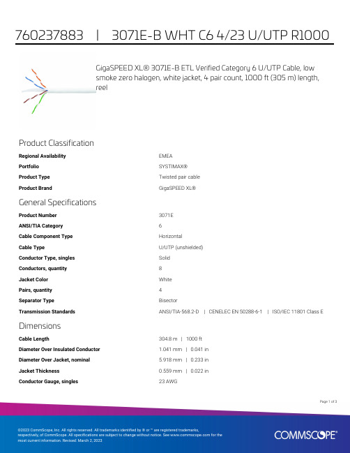
GigaSPEED XL® 3071E-B ETL Verified Category 6 U/UTP Cable, lowsmoke zero halogen, white jacket, 4 pair count, 1000 ft (305 m) length,reelProduct ClassificationRegional Availability EMEAPortfolio SYSTIMAX®Product Type Twisted pair cableProduct Brand GigaSPEED XL®General SpecificationsProduct Number3071EANSI/TIA Category6Cable Component Type HorizontalCable Type U/UTP (unshielded)Conductor Type, singles SolidConductors, quantity8Jacket Color WhitePairs, quantity4Separator Type BisectorTransmission Standards ANSI/TIA-568.2-D | CENELEC EN 50288-6-1 | ISO/IEC 11801 Class E DimensionsCable Length304.8 m | 1000 ftDiameter Over Insulated Conductor 1.041 mm | 0.041 inDiameter Over Jacket, nominal 5.918 mm | 0.233 inJacket Thickness0.559 mm | 0.022 inConductor Gauge, singles23 AWG13Page ofCross Section DrawingElectrical Specificationsdc Resistance Unbalance, maximum 5 %dc Resistance, maximum7.61 ohms/100 m | 2.32 ohms/100 ftDielectric Strength, minimum2500 VdcMutual Capacitance at Frequency 5.6 nF/100 m @ 1 kHzNominal Velocity of Propagation (NVP)70 %Operating Frequency, maximum300 MHzOperating Voltage, maximum80 VRemote Powering Fully complies with the recommendations set forth by IEEE 802.3bt (Type4) for the safe delivery of power over LAN cable when installed accordingto ISO/IEC 14763-2, CENELEC EN 50174-1, CENELEC EN 50174-2 or TIATSB-184-ASegregation Class cMaterial SpecificationsConductor Material Bare copperInsulation Material PolyolefinJacket Material Low Smoke Zero Halogen (LSZH)Separator Material PolyolefinPage of23Mechanical SpecificationsPulling Tension, maximum11.34 kg | 25 lbEnvironmental SpecificationsInstallation temperature0 °C to +60 °C (+32 °F to +140 °F)Operating Temperature-20 °C to +60 °C (-4 °F to +140 °F)Acid Gas Test Method EN 50267-2-3EN50575 CPR Cable EuroClass Fire Performance B2caEN50575 CPR Cable EuroClass Smoke Rating s1aEN50575 CPR Cable EuroClass Droplets Rating d0EN50575 CPR Cable EuroClass Acidity Rating a1Environmental Space Low Smoke Zero Halogen (LSZH)Smoke Test Method IEC 61034-2Packaging and WeightsCable weight38.097 kg/km | 25.6 lb/kftPackaging Type ReelRegulatory Compliance/CertificationsAgency ClassificationCENELEC EN 50575 compliant, Declaration of Performance (DoP) availableCHINA-ROHS Below maximum concentration valueISO 9001:2015Designed, manufactured and/or distributed under this quality management system REACH-SVHC Compliant as per SVHC revision on /ProductCompliance ROHSCompliantPage of33。
艾奇安防产品说明书

Privacy Mask Text Overlay Image Orientation
• Audio
Compression Audio-In Audio-Out
• Network
Protocol &larm
Simultaneous dual streams based on two configurations 28 Kbps - 6 Mbps (per stream) Constant, Variable
Basic WDR (74 dB); White balance: automatic, hold, and manual; Brightness; Contrast; Sharpness (auto); Auto gain control; Digital noise reduction; Flickerless
Hemispheric
Dome
Bullet
Box
PRODUCT SPECIFICATION
E81A
• Device
Device Type Image Sensor Sensor Size Day / Night Superior Low Light Sensitivity Minimum Illumination Color to B/W Switch Mechanical IR Cut Filter IR Sensitivity Range IR LED IR Working Distance Electronic Shutter
PHOTO INDICATION
3 4
1 2
1 Reset Button 2 Memory Card Slot 3 Reset Button
松下 数码相机 DC-G95 使用说明书
• 请勿使用其他任何 USB 连接电缆,只使用提供的 USB 连接电缆。 • 请务必使用正品的 Panasonic 快门遥控(DMW-RS2: 可选件)。 • 请使用带 HDMI 标志的 “High Speed HDMI micro 电缆 ”。 不符合 HDMI 标准的电缆不会工作。 “High Speed HDMI micro 电缆 ”(D 型 –A 型插头,最长 2 m) • 请勿使用长度在 3 m 以上的耳机电缆。 • 请勿使用 3 m 以上长度的立体声麦克风电缆。
Wi-Fi/Bluetooth
可以用 Wi-Fi®/Bluetooth® 功能做什么 ....................................62 连接到智能手机 .............................64 使用智能手机操作相机 ..................69
使本机尽可能远离电磁设备(如微波炉、电视机、视频游戏机等)。 • 如果在电视机上方或其附近使用本机,本机上的图像和 / 或声音可能会受到电磁 波辐射的干扰。 • 请勿在移动电话附近使用本机,因为这样可能会产生对图像和 / 或声音的品质有 负面影响的噪点。 • 扬声器或大型电机产生的强磁场,可能会损坏拍摄的数据或使图像失真。 • 电磁波辐射可能会对本机产生负面影响,以致干扰图像和 / 或声音。 • 如果本机由于受电磁设备的影响而停止正常工作,请关闭本机,并取出电池或拔 下交流电源适配器。 然后,重新插入电池或者重新连接交流电源适配器并开启本 机。
SKF0106K 8
K1HY04YY0106
SKF0145K
• 在本文中,SD 记忆卡、SDHC 记忆卡和 SDXC 记忆卡统称为记忆卡。 • 记忆卡为可选件。 • 本使用说明书是以可互换镜头 (H-FS12060) 为例来进行说明的。 • 在某些地区,可能不销售某些数码相机套装。 • 如果不慎丢失了提供的附件,请向经销商或离您最近的服务中心咨询。
Infineon TC265DE模拟适配器硬件用户手册V2.0,2023年11月说明书

V2.0, November 2023/startGeneral safety instructionsPlease read the following safety precautions carefully before putting this device to use to avoid any personal injuries, damage to the instrument, or to the target system. Use this instrument only for its intended purpose as specified by this manual to prevent potential hazards.Use included power cord and power supplyThe enclosed power supply has been approved for use by iSYSTEM. Please contact iSYSTEM if you need to consider an alternative power.Use grounding wirePrior to applying power to either the BlueBox or the target, connect the device and the target sys-tem together with the included grounding wire. This is to avoid potential damage caused by any voltage difference between the device and the target system.Use proper overvoltage protectionEnsure proper protection to avoid exposing the BlueBox device or the operator to overvoltage surges (e.g. caused by thunderstorm, mains power).Do not operate without coverDo not operate the device with cover removed.Avoid circuit and wire exposureDo not touch exposed components or wires when the device is powered.Do not operate with suspected damageIf you suspect damage may have occurred, the BlueBox device must be inspected by qualified service personnel before further operation.Do not operate the device outside its rated supply voltage or environ-mental rangeConsult with iSYSTEM before using equipment outside of the parameters provided in this manual.Contents Introduction (4)Package content (5)Adaptation packages content (6)Operation (7)Adaptation setup (8)Screws (9)Configuration (10)Connectors (13)Power supply package (14)Standalone operation (15)Measurement board (16)Mechanical information (17)Schematics (19)Infineon TC265DE Emulation Adapter primary use case is providing AURORA GigaBit Trace (AGBT) functionality for the TC265 device in the QFP144 package featuring no trace functional-ity. The Emulation Adapter is based on the 216-pin emulation device.The Emulation Adapter might differ in some peripherals from the target device; there-fore, the device datasheet should be checked.Alternative use case is a Standalone operation. In this case customer can start developing and testing the application while his target may not be available yet.Complete emulation adapter is split into individual parts which makes it flexible when support for different target packages is required. A typical setup in conjunction with the target contains:·IEA-TC265DE (Microcontroller part)·Conversion board·Solder partThe emulation adapter can be used in conjunction with iC6000 debug and test tool or other third-party tools supporting AGBT interface for Infineon Aurix family. The tool connects to 22-pin Samtec ERF8 connector (P1) providing the DAP debug and the AGBT interface connection.More information about our products onInfineon TC265 Emulation Adapter is delivered with all components required for Standalone op-eration. Adaptation package for the Target board adaptation and the Power adapter must be ordered separately.Infineon TC265 Emulation AdapterPower supply packagePower converter Power adapterOrdering code: IEA-TC265DE Ordering code:IEA-PSOrdering code:IT9V-PSGND Wire Measurement board (optional)Ordering code: BB-WIRE Ordering code: IAMTC265DEConversion boards connect between the Emulation Adapter and the matching Solder part which is being soldered on the Target side.Fixed AdaptationThe adaptation is elivered with a slot screw, which can be used to achieve a more solid and stable fixing of the Conversion board and the Solder part.Conversion board Solder partEmulation Adapter offers the following adaption setup:·Fixed AdaptationTop / Bottom side of the Emulation Adapter Introduction to Emulation Adapter (video)/ea-intro How to connect Hardware (video)/connect-hardwareFixed AdaptationSlot screwThe Slot screw (30mm) is used to fix the Conversion board to the Solder part. The setup be-comes mechanically more robust.Screw the Conversion board to the Solder part first, before the Emulation Adapter is attached on top and watch out not to break out the Solder part, e.g., if you accidentally hit the Emulation Adapter from the side.Short Hexagon socket screwShort Hexagon socket screw, which comes with the Solder part, is not applicable with this Emu-lation Adapter setup.J1: Target reset configurationJumper J1 connects the TC265DE reset line (PORST) and the target reset line. By default J1 is populated.When having problems establishing the initial debug session with the emulation adapter, try to remove J1 and see if it makes any difference.J2 and J3: Clock source configurationJumpers J2 and J3 select clock source for the microcontroller on the emulation adapter.Per default, both jumpers are set to position 1-2, which yields the clock source being used from the target.Note that the emulation adapter may not operate when crystaltarget. Typical design guideline is that the crystal should be as close as possible to themicrocontroller. However, it may happenconjunction with the emulation adapter since clock lines (XTAL1, XTAL2) between thetarget and the emulation device on the emulation adapter can become too long, con-sequentially affecting the impedance of the crystal circuit too much. There should beno problem if the oscillator is used in the target.If an oscillator in the target is not an option and the target crystal doesn’t oscillate in conjunc-tion with the emulation adapter, clock from the emulation adapter must be used (J2 & J3 posi-tion 2-3). In this case, a crystal circuit must be assembled on the emulation adapter. Below Crys-tal socket. Crystal circuit is located in the corner of the emulation adapter, next to the connector P1.Per default 10pF capacitors are populated for C1 and C2 and thecrystal Q3 is not populated. Note that C1 and C2 values are validfor 20MHz crystal only. If different crystal is used, the default 10pF capacitors must be replaced with proper value.J5 & J6: GND connecting pointsJ5 and J6 provide grounding points on the Emulation Adapter.In case a good ground connection is required, connection pointsbridge J5 and pin J6 provide easy access to the emulation adapterGND potential.Startup and Power Supply ModeThe target device TC265 being emulated with this emulation adapter, can have the external nominal system supply either 3.3V or 5V. Both are supported by the emulation adapter. The power supply scheme of the TC265DE at startup is based on the latched status of HWCFG[0:2] pins before PORST release. With the emulation adapter, HWCFG[0:2, 6] pins are left unconnected (floating) while the TC265DE PORST signal is low. This ensures embedded voltage regulators EVR33 and EVR13 are active by default. As soon as the PORST line is released from the low state, the HWCFG[0:2, 6] pins get connected to the target via the emulation adapter logic.P2: Power supply configurationNC – Not ConnectedRefer to the microcontroller user’s manual for more details which power supply designation in the above table belongs to which power supply.By default all jumpers are set and connect target power supply coming from the target to the mi-crocontroller residing on the emulation adapter. In principle, pins 3-4, 5-6, 7-8, must be bridged only but for the convenience and ease of use all jumpers are set, except for pins 25-26. Pin 26 is the polarizer key preventing incorrect connection of the IEA-PS power supply, when connected.P1: AURORA trace portBlue colored signals are AGBT interface signals.Signal Direction is described from the BlueBox perspective.Be aware that debug and trace signals from the Emulation adapter superset device are not connected toEmulation adapter.A Power supply package, which is delivered with the Emulation Adapter, is required when:·The Emulation Adapter is used as a standalone device .·The target board doesn’t provide an accurate supply voltage.·The target board doesn’t provide sufficient current for the Emulation Adapter operation.The Power converter can supply either 3.3 V or 5 V. Array of jumpers J0 – J9 select 3.3 V or 5 V voltage on the P3 connector, which connects to the Emulation Adapter.For example, when J2 is in the 3V3 position, it supplies 3.3 V to pin 6 of the P3 connector. When J2 is in 5V position, it supplies 5 V to pin 6 of the P3 connector pin.Be careful not toclared maximum voltage 3.3 V! Refer to microcontroller documentation for detailed in-formation.External power supply requirements:Emulation Adapter is delivered with all components required for a Standalone operation.Power supplyUse enclosed IEA-PS Emulation Adapter Power converter and adapter.When having problems getting the emulation adapter operational in conjunction with the target, emulation adapter standalone operation should be tested first. In this case, minimally the IEA-TC265DE emulation adapter and the IEA-PS power supply connecting to the emulation adapter P2 connector (all jumpers must be removed from P2 prior) are required only.When the emulation adapter is connected to the target and configured for operation with power supply from the target, power supply IEA-PS is not required nor it can be connected since P2 un-shrouded 26-pin 2.54mm header is populated with jumpers.If a different power source is to be used (e.g. in case of a standalone operation), all jumpers must be removed and power source must be applied to CVEXT (pin 4), CVDDM (pin 6), and CVFLEX (pin 8) signals. The emulation adapter comes delivered together with the IEA-PS emula-tion adapter power supply, which simply plugs into the P2 header row, providing the necessary power supply for emulation adapter standalone operation. Double check that the IEA-PS emula-tion adapter power supply is configured properly for this particular emulation adapter.With the Measurement board you gain easy access to all MCU pins respectively, because mod-ern targets do not have accessible all the MCU pins / connected signals to connect with a meas-urement equipment (oscilloscope, logic analyzer).The Measurement board is optional and connects between the Emulation Adapter and the Con-version Board. It comes together with an applicable Layout board (black panel where all the CPU signals are nicely marked) that matches your order. The black panel is placed over the Measure-ment board.Top view of the Measurement board Layout board example for the MeasurementboardNot available in every Emulation Adapter or every MCU pin count.Side view of the Solder part Solder part solder pad view Top view of the Solder partSide view of the Emulation adapter complete setup - QFP Fixed Adaptation Top view of the EmulationAdapterTop view of the Conversion boardSolder partsIn the case of soldering the Solder part manually, it’s highly recommended to prolong the solder pad E on the outer side (e.g., for 1.5–2 mm) during the PCB design. Note that without this modi-fication, it’s very difficult to solder the Solder part manually.Use the Surface Mount Technology (SMT) to solder the Solder parts to the user target board instead of the original microcontroller. iSYSTEM provides this soldering service on request too.To view Emulation Adapter schematics, use the short link /schematics. Below is a pinout of the four connectors P3-P6 on the bottom side of the emulation adapter:NC – Not ConnectedGreen marked squares – Voltage pinsOptionally, the user could also design his target directly providing connection for the emulation adapter via the P3-P6 connectors. Connectors being used on the emulation adapter side are TE connectivity fe-male connectors, part number: 0-0104652-4 (40-pin connector) and 0-0104652-6 (60-pin connector). The target must feature male matching connectors.Visit our website for:·Support - /support ·Tutorials - /start ·Knowledge Base - 。
infinix i销售手册

新产品弥补了旧产品的哪些不足
项目 全面的网络能力 DICOM 比较 infinix VC/CC CDR, infinix-I VC/CC XA Image SCU, Query/Retrieve, SCP (Option) 备注
手动传送/背景 自动传送/背景工作 工作 uECG 波形数据刻录 图像刻录 uStorage Commitment storage (Option)
-i series
产品销售引导
-i series
基本概念
血管造影中那些性能医生最感兴趣
1. 图像质量-图像质量清晰,可以减少透视时间,减少手术中
的射线剂量;可以减少图像回访观察时间,缩短手术进程,增加 手术安全。
2. 方便程度-操作的手术医生一般最关注临床和手术本身的过
程,希望设备的操作对医生的影响最小化。
3. 手术安全及设备稳定性-介入手术虽然以微创,高效
为特征,但是对于操作医生以内科等非外科专业为主,同时手术 本身也存在这很大的风险,所以手术过程的安全保障往往比普通 的手术更为必要和紧迫。对于设备来说,能为手术过程提供最大 可能的安全保障措施,是医生非常感兴趣的。
4. 医生安全-所有的过程人的地位是最重要的,这是“科技以
2. 方便程度-操作装置的智能化程度、系统并行处理能力、网络的连接能力
“一键通”智能导航操作系统 互交式床旁操作装置 智能单手柄 真正的全功能并行多任务执行能力 开放式CDR、全功能DICOM接入(光盘图像可以回到主机, 飞利浦及西门子也可以但不是DICOM格式)
东芝的DSA在关键参数上的优势
3. 手术安全-设备出现故障时保证手术安全结束的能力、病人手术数据的安全
人为本”的要旨所在,对医生而言,病人和自己的安全都是不可 或缺的,尤其为病人解决病痛的同时,使自己受到最小的影响, 更是工作的原则,但是介入手术却是为病人治病,而使自己受到 伤害,
卡萨帝家用直流变频空调 CAS351UDA(81)U1说明书

CAS261UBA(81)U1(SKFR-26GW/01UBA81KU1)CAS351UBA(81)U1(SKFR-35GW/01UBA81KU1)CAS261UCA(81)U1(SKFR-26GW/01UCA81KU1)CAS351UCA(81)U1(SKFR-35GW/01UCA81KU1)CAS261UDA(81)U1(SKFR-26GW/01UDA81KU1)CAS351UDA(81)U1(SKFR-35GW/01UDA81KU1)CAS261UEA(81)U1(SKFR-26GW/01UEA81KU1)CAS351UEA(81)U1(SKFR-35GW/01UEA81KU1)智能家电操控智慧场景定制智家商城购物家电报装报修卡萨帝为了精确实现您的格调生活,对其家族每一类产品都赋予了专属的境界理念。
本产品为您带来的是冷暖舒适。
12关于本产品的安全注意事项.........................................................3本产品的安装事项 (5)使用方面.............................................................................6随机附件 (6).................................................7室内外机安装图...................................................................7安装(按照室内机组安装图进行安装).................................8管路系统图...........................................................................8安装检查及试运转................................................................8室内机管路布置.................................................9接线方法 (10)室内外机接线..................................................................排空方法(R32)......................................................11本产品的外观及部件介绍.. (12)室内机................................................................................12室内机显示面板.................................................................12室外机................................................................................12遥控器.................................................................................13本产品的主要功能介绍 (15)1.时钟校准..............................................................................................................................................152.定时功能153.自动化空气调节(制冷、制热、辅热、除湿).............174.设置温度.....................................................................5.调节风向.....................................................................6.自清洁功能..................................................7.IFD除尘/负离子功能188.温度显示2210.停电补偿功能2311.静眠功能......................................................................2012.21本产品的日常保养与维护24空气过滤网的安装24清洗机器.............................................................24换季收存24有疑问?先看这儿!25(若对空调有疑问,请先按本章内容检查处理。
公共安全一类视频监控点方案

社会治安一类点监控视频监控系统方案1目录1.概述 (3)1.1系统概述 (5)1.1.1 系统应用概述 (5)1.1.2 实现功能简述 (6)1.2设计目标 (6)1.2.1架构合理 (7)1.2.2稳定性和安全性 (7)1.2.3产品主流 (7)1.2.4低成本低维护量 (8)1.3系统设计原则 (9)1.3.1先进性 (9)1.3.2安全性 (9)1.3.3可扩充性 (9)1.3.4规范性 (9)1.4系统设计依据 (9)2.系统总体设计方案 (10)2.1设计概述 (10)2.1.1前端部分 (11)2.1.2控制部分 (12)2.1.3传输部分 (13)2.1.4显示与记录 (13)2.2设计功能描述 (13)1.1.3 总体设计方案 (14)1.1.4 主控中心机房设计 (14)1.1.5 提出方案 (15)1.1.6 整体系统结构图 (17)1.1.7 前端设备 (18)1.1.8 系统存储 (18)1.1.9 传输方式 (18)3.系统特色功能介绍 (19)3.1集散式监控 (19)3.2编码传输功能 (19)3.3网络视频集中监控系统管理软件 (19)3.4网络并发连接的功能 (20)3.5显示功能 (20)3.6录像功能 (20)3.7智能化检索回放功能 (21)3.8系统分级管理 (22)3.9云台镜头控制功能 (22)3.10主要产品介绍 (23)4.售后服务与人员培训 (33)4.1售后服务 (33)4.2人员培训 (34)5.设备清单 (36)1.概述随着经济的发展、城镇建设速度加快,导致城市中人口密集、流动人口增加,引发了城市建设中的交通、社会治安、重点区域防范等城市管理问题。
尤其是近年来面对城市反恐的新课题,为公安管理工作特别是预防犯罪和执法工作提出了新的挑战。
而公安警力增加远不能满足实际需求的发展速度,于是能将科技手段转化为直接战斗力的城市治安图像监控成为了解决该问题的重要手段。
Richtek技术有限公司产品说明书

RT8511B®DS8511B-05 February 20151©Copyright 2015 Richtek Technology Corporation. All rights reserved. is a registered trademark of Richtek Technology Corporation.Ordering InformationNote :Richtek products are :❝ RoHS compliant and compatible with the current require-ments of IPC/JEDEC J-STD-020.❝ Suitable for use in SnPb or Pb-free soldering processes.Marking InformationPin Configurations(TOP VIEW)WDFN-8L 2x243V Asynchronous Boost WLED DriverGeneral DescriptionThe RT8511B is an LED driver IC that can support up to 10 WLED in series. It is composed of a current mode boost converter integrated with a 43V/2.2A power switch running at a fixed 500kHz frequency and covering a wide VIN range from 2.7V to 24V.The white LED current is set with an external resistor, and the feedback voltage is regulated to 200mV (typ.). During operation, the LED current can be controlled by the PWM input signal in which the duty cycle determines the feedback reference voltage.For brightness dimming, the RT8511B is able to maintain steady control of the LED current. Therefore, no audible noises are generated on the output capacitor. The RT8511B also has programmable over voltage pin to prevent the output from exceeding absolute maximum ratings during open LED conditions. The RT8511B is available in WDFN-8L 2x2 package.Features●Wide Input Voltage Range : 2.7V to 24V●High Output Voltage : up to 43V●Direct PWM Dimming Control and Frequency from 100Hz to 8kHz●Internal Soft-Start and Compensation ●200mV Reference Voltage●PWM Dimming with Internal Filter●Programmable Over Voltage Protection ●Over Temperature Protection ●Current Limit Protection ●Thin 8-Lead WDFN Package●RoHS Compliant and Halogen FreeApplications●UMPC and Notebook Computer Backlight ●GPS, Portable DVD BacklightEN PWM VIN LX0F : Product CodeW : Date CodeG : Green (Halogen Free and Pb Free)RT8511BRT8511B2DS8511B-05 February 2015 ©Copyright 2015 Richtek Technology Corporation. All rights reserved. is a registered trademark of Richtek Technology Corporation.Typical Application CircuitFigure 1. Typical Application Circuit of Normal OperationFigure 2. Typical Application Circuit of Low Voltage OperationVSET SETRT8511B3DS8511B-05 February 2015©Copyright 2015 Richtek Technology Corporation. All rights reserved. is a registered trademark of Richtek Technology Corporation.Function Block DiagramRT8511B4DS8511B-05 February 2015©Copyright 2015 Richtek Technology Corporation. All rights reserved. is a registered trademark of Richtek Technology Corporation.Electrical CharacteristicsRecommended Operating Conditions (Note 4)●Supply Input Voltage, V IN ------------------------------------------------------------------------------------------------2.7V to 24V ●Junction T emperature Range --------------------------------------------------------------------------------------------−40°C to 125°C ●Ambient T emperature Range --------------------------------------------------------------------------------------------−40°C to 85°CAbsolute Maximum Ratings (Note 1)●VIN, EN, PWM, DIMC to GND------------------------------------------------------------------------------------------−0.3V to 26.5V ●FB, OVP to GND ----------------------------------------------------------------------------------------------------------−0.3V to 48V ●LX to GND ------------------------------------------------------------------------------------------------------------------−0.3V to 48V < 500ns ----------------------------------------------------------------------------------------------------------------------−1V to 48V ● Power Dissipation, P D @ T A = 25°CWDFN-8L 2x2--------------------------------------------------------------------------------------------------------------0.833W ●Package Thermal Resistance (Note 2)WDFN-8L 2x2, θJA ---------------------------------------------------------------------------------------------------------120°C/W WDFN-8L 2x2, θJC ---------------------------------------------------------------------------------------------------------8.2°C/W ●Lead Temperature (Soldering, 10 sec.)-------------------------------------------------------------------------------260°C ●Junction T emperature -----------------------------------------------------------------------------------------------------150°C●Storage T emperature Range --------------------------------------------------------------------------------------------–65°C to 150°C ●ESD Susceptibility (Note 3)HBM (Human Body Model)----------------------------------------------------------------------------------------------2kV MM (Machine Model)-----------------------------------------------------------------------------------------------------200VRT8511B5DS8511B-05 February 2015©Copyright 2015 Richtek Technology Corporation. All rights reserved. is a registered trademark of Richtek Technology Corporation.Note 1. Stresses beyond those listed “Absolute Maximum Ratings ” may cause permanent damage to the device. These arestress ratings only, and functional operation of the device at these or any other conditions beyond those indicated in the operational sections of the specifications is not implied. Exposure to absolute maximum rating conditions may affect device reliability.Note 2. θJA is measured at T A = 25°C on a high effective thermal conductivity four-layer test board per JEDEC 51-7. θJC ismeasured at the exposed pad of the package.Note 3. Devices are ESD sensitive. Handling precaution is recommended.Note 4. The device is not guaranteed to function outside its operating conditions.RT8511B6DS8511B-05 February 2015 ©Copyright 2015 Richtek Technology Corporation. All rights reserved. is a registered trademark of Richtek Technology Corporation.LED Current vs. PWM Duty Cycle1020304050600102030405060708090100PWM Duty Cycle (%)L E D C u r r e n t (m A)Typical Operating CharacteristicsFB Reference Voltage vs. Input Voltage198.0198.3198.6198.9199.2199.54812162024Input Voltage (V)F B R e f e r e n c e V o l t a g e (m V)Frequency vs. Input Voltage3504004505005506004812162024Input Voltage (V)F r e q u e n c y (k H z ) Efficiency vs. Input Voltage6065707580859095100479121417192224Input Voltage (V)E f f i c i e n c y (%)FB Reference Voltage vs. Temperature-205305580105Temperature (°C)Current Limit vs. Input Voltage1.01.41.82.22.63.02.55.25810.7513.516.251921.7524.5Input Voltage (V)C u r r e n t L i m i t (A )RT8511B7DS8511B-05 February 2015©Copyright 2015 Richtek Technology Corporation. All rights reserved. is a registered trademark of Richtek Technology Corporation.Application InformationThe RT8511B is a current mode boost converter which operates at a fixed frequency of 500kHz. It is capable of driving up to 10 white LEDs in series and integrates functions such as soft-start, compensation, and internal analog dimming control. The protection block also provides over-voltage, over-temperature, and current- limit protection features.LED Current SettingThe loop structure of the boost converter keeps the FB pin voltage equal to the reference voltage V FB . Therefore,by connecting the resistor, R SET between the FB pin and GND, the LED current will be determined by the current through R SET . The LED current can be calculated by the following equation :FBLED SET VI = R Brightness ControlFor the brightness dimming control of the RT8511B, the IC provides typically 200mV reference voltage when the PWM pin is constantly pulled high. However, the PWM pin allows a PWM signal to adjust the reference voltage by changing the PWM duty cycle to achieve LED brightness dimming control. The relationship between the duty cycle and the FB voltage can be calculated according to the following equation :V FB = 200mV x Dutywhere 200mV is the typical internal reference voltage and Duty is the duty cycle of the PWM signal.As shown in Figure 3, the duty cycle of the PWM signal is used to modify the internal 200mV reference voltage.With an on-chip output clamping amplifier and a serial resistor, the PWM dimming signal is easily low-pass filtered to an analog dimming signal with one external capacitor, C DIMC , for noise-free PWM dimming. Dimming frequency can be sufficiently adjusted from 100Hz to 8kHz.However, the LED current cannot be 100% proportional to the duty cycle. Referring to T able 1, the minimum dimming duty can be as low as 1% for the frequency range from 100Hz to 8kHz. It should be noted that the accuracy of 1% duty is not guaranteed.Figure 3. Block Diagram of Programmable FB Voltage Table 1. Minimum Duty for Dimming FrequencyBecause the voltage of DIMC and FB is small to 2mV andeasily affected by LX switching noise.ToControllerThe FB pin voltage will be decreased by lower PWM duty ratio . That will achieve LED current diming function for different brightness. But LED current is more accurate when higher PWM duty. The Table 2. shows typical variation value comparison between different PWM duty and condition is V IN = 3.7V, LED array = 6S2P , R SET =5Ω.Table 2. LED Current Variation vs PWM DutyIt also should be noted that when the input voltage is too close to the output voltage [(V OUT −V IN ) < 6V] , excessive audible noise may occur. Additionally, for accurate brightness dimming control, the input voltage should be kept lower than the LEDs' turn on voltage. When operating in the light load, excessive output ripple may occur.RT8511B8DS8511B-05 February 2015 ©Copyright 2015 Richtek Technology Corporation. All rights reserved. is a registered trademark of Richtek Technology Corporation.Mode2Mode3Figure 4. Power On SequenceMode1Mode3Figure 5. Power Off SequenceV INV OUTENV INV OUTENPWMV INV OUTENPWMV INV V INV OUTENPWMDelayMode1V INV ENSoft-StartThe RT8511B provides a built-in soft-start function to limit the inrush current, while allowing for an increased PWM frequency for dimming.Current Limiting ProtectionThe RT8511B can limit the peak current to achieve over current protection. The IC senses the inductor current through the LX pin in the charging period. When the value exceeds the current limiting threshold, the internal N-MOSFET will be turned off. In the off period, the inductor current will descend. The internal MOSFET is turned on by the oscillator during the beginning of the next cycle.Power SequenceIn order to assure that the normal soft-start function is in place for suppressing the inrush current, the input voltage and enable voltage should be ready before PWM pulls high. Figure 4 and Figure 5 show the power on and power off sequences.RT8511B9DS8511B-05 February 2015©Copyright 2015 Richtek Technology Corporation. All rights reserved. is a registered trademark of Richtek Technology Corporation.OUT, OVP OVP R2V = V 1+R1⎛⎫⨯ ⎪⎝⎭where R1 and R2 make up the voltage divider connected to the OVP pin.Over Temperature ProtectionThe RT8511B has an Over T emperature Protection (OTP)function to prevent overheating caused by excessive power dissipation from overheating the device. The OTP will shut down switching operation if the junction temperature exceeds 160°C. The boost converter will start switching again when the junction temperature is cooled down by approximately 30°C.Inductor SelectionThe inductance depends on the maximum input current.As a general rule, the inductor ripple current range is 20%to 40% of the maximum input current. If 40% is selected as an example, the inductor ripple current can be calculated according to the following equation :OUT OUTIN(MAX)(MIN)IN(MIN)RIPPLE IN(MAX)V I I =V I = 0.4I η⨯⨯⨯where η is the efficiency of the boost converter, I IN(MAX) is the maximum input current, I OUT is the total current from all LED strings, and I RIPPLE is the inductor ripple current.The input peak current can be calculated by maximum input current plus half of inductor ripple current shown as following equation :I PEAK = 1.2 x I IN(MAX)Note that the saturated current of the inductor must be greater than I PEAK . The inductance can eventually be determined according to the following equation :Over Voltage ProtectionThe RT8511B equips Over Voltage Protection (OVP)function. When the voltage at the OVP pin reaches a threshold of approximately 1.2V , the MOSFET drive output will turn off. The MOSFET drive output will turn on again once the voltage at the OVP pin drops below the threshold.Thus, the output voltage can be clamped at a certain voltage level, as shown in the following equation :()())2IN OUT IN 2OUT OUT OSCV (V V L =0.4V I f η⨯⨯-⨯⨯⨯where f OSC is the switching frequency. For better efficiency,it is suggested to choose an inductor with small series resistance.Diode SelectionThe Schottky diode is a good choice for an asynchronous boost converter due to its small forward voltage. However,when selecting a Schottky diode, important parameters such as power dissipation, reverse voltage rating, and pulsating peak current must all be taken into consideration. A suitable Schottky diode's reverse voltage rating must be greater than the maximum output voltage,and its average current rating must exceed the average output current.Capacitor SelectionTwo 1μF ceramic input capacitors and two 1μF ceramic output capacitors are recommended for driving 10 WLEDs in series. For better voltage filtering, ceramic capacitors with low ESR are recommended. Note that the X5R and X7R types are suitable because of their wide voltage and temperature ranges.Thermal ConsiderationsFor continuous operation, do not exceed absolute maximum junction temperature. The maximum power dissipation depends on the thermal resistance of the IC package, PCB layout, rate of surrounding airflow, and difference between junction and ambient temperature. The maximum power dissipation can be calculated by the following formula :P D(MAX) = (T J(MAX) − T A ) / θJAwhere T J(MAX) is the maximum junction temperature, T A is the ambient temperature, and θJA is the junction to ambient thermal resistance.For recommended operating condition specifications, the maximum junction temperature is 125°C. The junction to ambient thermal resistance, θJA , is layout dependent. For WDFN-8L 2x2 package, the thermal resistance, θJA , is 120°C/W on a standard JEDEC 51-7 four-layer thermal test board. The maximum power dissipation at T A = 25°C can be calculated by the following formulas :RT8511B10DS8511B-05 February 2015 ©Copyright 2015 Richtek Technology Corporation. All rights reserved. is a registered trademark of Richtek Technology Corporation.Figure 7. PCB Layout GuideLayout ConsiderationFor high frequency switching power supplies, the PCBlayout is important to obtain good regulation, high efficiency and stability. The following descriptions are the suggestions for better PCB layout.❝Input and output capacitors should be placed close to the IC and connected to the ground plane to reduce noise coupling.❝The GND and Exposed Pad should be connected to a strong ground plane for heat sinking and noise protection.❝The components L, D, C IN and C OUT must be placed as close as possible to reduce current loop. Keep the main current traces as possible as short and wide.❝The LX node of the DC/DC converter experiences is with high frequency voltage swings. It should be kept in a small area.❝The component R SET should be placed as close as possible to the IC and kept away from noisy devices.Figure 6. Derating Curve of Maximum Power DissipationP D(MAX) = (125°C − 25°C) / (120°C/W) = 0.833W for WDFN-8L 2X2 packageThe maximum power dissipation depends on operating ambient temperature for fixed T J(MAX) and thermal resistance, θJA . The derating curves in Figure 6 allow the designer to see the effect of rising ambient temperature on the maximum power dissipation.0.00.20.40.60.81.0255075100125Ambient Temperature (°C)M a x i m u m P o w e r D i s s i p a t i o n (W )IN as closed as possible to V I N pin for good filtering.directly from the output schottky diode to ground rather than across the WLEDs.The inductor should be placed as close as possible to theswitch pin to minimize the noise coupling into other circuits.LX node copper area should be minimized for reducing EMILocate R SET closeW-Type 8L DFN 2x2 PackageRichtek Technology Corporation14F, No. 8, Tai Yuen 1st Street, Chupei CityHsinchu, Taiwan, R.O.C.Tel: (8863)5526789Richtek products are sold by description only. Richtek reserves the right to change the circuitry and/or specifications without notice at any time. Customers should obtain the latest relevant information and data sheets before placing orders and should verify that such information is current and complete. Richtek cannot assume responsibility for use of any circuitry other than circuitry entirely embodied in a Richtek product. Information furnished by Richtek is believed to be accurate and reliable. However, no responsibility is assumed by Richtek or its subsidiaries for its use; nor for any infringements of patents or other rights of third parties which may result from its use. No license is granted by implication or otherwise under any patent or patent rights of Richtek or its subsidiaries.DS8511B-05 February 11。
UL2651-p15--日立标准
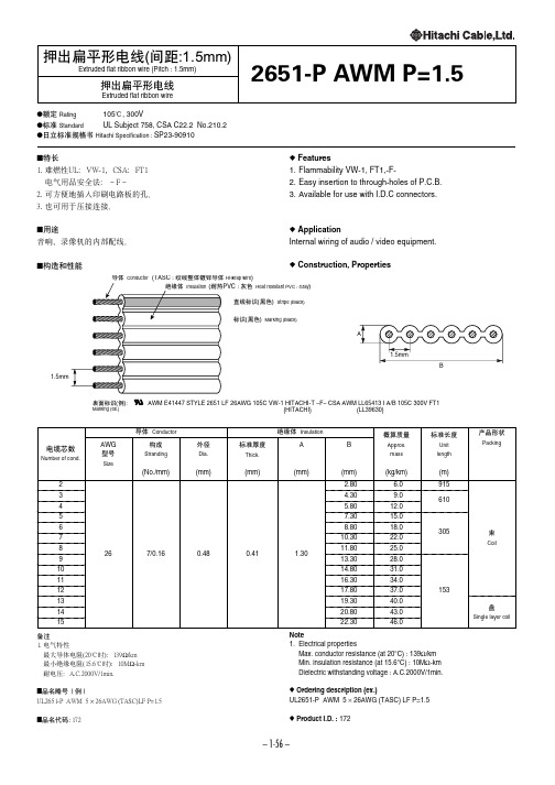
– 1-56 –●额定Rating 105℃, 300V●标准StandardUL Subject 758, CSA C22.2 No.210.2●日立标准规格书Hitachi Specification : SP23-90910■特长1.难燃性UL:VW-1,CSA:FT1电气用品安全法:-F-2.可方便地插入印刷电路板的孔。
3.也可用于压接连接。
■用途音响、录像机的内部配线。
■构造和性能◆Features1.Flammability VW-1, FT1,-F-2.Easy insertion to through-holes of P.C.B.3.Available for use with I.D.C connectors.◆ApplicationInternal wiring of audio / video equipment.◆Construction, Properties备注1.电气特性最大导体电阻(20℃时):139Ω/km 最小绝缘电阻(15.6℃时):10M Ω-km 耐电压:A.C.2000V/1min.■品名略号(例)UL2651-P AWM 5 ×26AWG (TASC)LF P=1.5■品名代码:172Note1.Electrical propertiesMax. conductor resistance (at 20°C) : 139Ω/km Min. insulation resistance (at 15.6°C) : 10M Ω-km Dielectric withstanding voltage : A.C.2000V/1min.◆Ordering description (ex.)UL2651-P AWM 5 ×26AWG (TASC) LF P=1.5◆Product I.D. : 172PVC : 灰色 Heat resistant PVC : Gray )Hi-wrap wire )直线标识(黑色) Stripe (Black)标识(黑色) Marking (Black)表面标识(例):AWM E41447 STYLE 2651 LF 26AWG 105C VW-1 HITACHI-T –F– CSA AWM LL65413 I A/B 105C 300V FT1Marking (ex.)(HITACHI)(LL39630)。
大恒SV系列摄像机使用说明书
PE-060(UL2651 30AWG线材规格书

變更日期 2008/10/29 變更內容 新增料號機種 品名 FLAT CABLE 30AWG 材質 PH:1.27MM(0.05'') 導體:見附表 絕緣:PVC 檢查頻率見巡檢報表
CONSTRUCTION TABLE Size of conductor Code NO. Composition AWG (strands/mm 9P 30 1/0.254
核准 文件編號 版本/III-PE-60
A2
1/1
FFC
泓翔精密電子科技(東莞)有限公司
A± 0.10
B± 0.10
C± 0.02
料號 M4004-0002
品名描述 9P單芯灰排(GY-42), 1/0.254mm銅線,桃紅邊 9P單芯黑排, 1/0.254mm銅線,白邊
偏心率(mm)
11.43
10.16
0.90 M4004-0003
左右偏0.01,
上下偏0.025
1. Voltage Raring (額定電壓):300V 2. Temperature Rating (額定溫度) :105℃ 3. Spark Test (火花測試):3.0KV/0.15sec Min. 4. Dielectric Strength (耐壓強度):2.0KV 60HZ 1 Minute (No Break Down) 5. Insulation Resistance (絕緣阻抗):100MΩ/M MIN AT DC 500V 6. Tensile strength Before Aging (老化前抗張強度):1500PSL Tensile Strength After Aging (老化後抗張強度):70% MIN.(136℃*168H) 7. Elongation Before Aging (老化前引伸) 100% MIN. Elongation After Aging (老化後引伸) :65% MIN.(136*168H) 8. Deformation Test (變形測試):50% MAX.(121℃*H) 9. Cold Bend Test (冷彎測試):-10℃*4H No Crack 10.導體直徑公差: ±0.003mm 11.印字內容: FFC AWM E253299 2651 105℃ 300V VW-1 30AWG
KNX产品手册

Light A
OFF
ON
90% Dimmer 1
OFF
ON
Shutter 2
UP
DOWN
Light B
OFF
30% Dimmer 2 OFF
ON ON
User 2
Room Temperature
21.4°
Shutter 1
UP
DOWN
U.motion 10寸触摸屏
Previous Floor Plan Living Room Bathroom Bedroom Nursery 1 Nursery 2
Light A
OFF
ON
90% Dimmer 1
OFF
ON
Shutter 2
UP
DOWN
Light B
OFF
30% Dimmer 2 OFF
ON ON
User 2
Room Temperature
21.4°
Shutter 1
UP
DOWN
U.motion 15寸触摸屏
4
在离开房间的时候,您是否希望 通过按下某个按键来确保所有的灯和 电器都已经关闭?您是否希望在早晨 按下某个按键放下百叶窗从而营造出 良好的光线氛围?
产品编号
包装单位
PG
MTN689701
5/2500
9
备注
款式 黄色/奶白
干线连接端子,黄色/奶白
干线连接端子由两个互相啮合的端子部件(黄色和 白色)租车组成,每个部件带4个插接式端口。适合 直径在0.6到0.8mm的实心导线。 用于为总线电缆的黄/白芯线布线。
产品编号
包装单位
PG
MTN689702
凌力尔特推出8通道电压/电流和温度监视器

感器 产 品组 合, 出小 型 高 性 能 三 轴模 拟 陀 螺仪 。 推
L G3 5 A 整 合 意 法半 导 体 已 生 产 近 l . 3 20 5 4亿 颗 运 动 传 感 。叠 萋 Nhomakorabea曩
誊 誊
j j
篓 『 童\  ̄
y
度 ; 系 统 精 度 的 8 8 n rHz低 噪 声 ; 入 共 模 范 围从 高 . V/t 输 负 轨 扩 展 到 正 轨 1 5V 内 , 但 可 节 省 其 他 电 路 系 统 , . 不 而
且 还 支 持 5V 单 电源 工 作 。
医 疗 设 备 、 物 识 别 安 防 、 控 家 庭 自动 化 以及 流 量 表 等 生 声
添加高级信号处理功能 。 TI可 为 US B音 频 类 与 人 机 接 口设 备 ( D)应 用 提 HI 供免费软件框架 , 够 便捷 地实施 实 时可靠 的音频 系统 , 能
如 耳 机 、 声 器 以及 录音 机 等 。 开 发 人 员 可 凭 借 丰 富 的 软 扬 件 构 建 各 种 解 决 方 案 , 不 但 可 插 入 US 其 B端 口 , 成 全 双 生
关频率 。
新 的 MHD选 件 可 自动 进 行 完 整 的 M HL一 致 性 测 试 , 且 可 获 得 更 高 的 测 试 效 率 、 高 的 生 产 率 和 更 可 靠 而 更
L 6 1包 括 一 个 用 于 每个 通 道 的 上 电 复 位 定 时 器 和 T3 4
一
的 结 果 。创 新 的 MHL 协 议 分 析 仪 ( MHL P ooo An— rtcl a
ul2651标准电线参数

ul2651标准电线参数
UL2651标准电线参数包括以下几个方面:
1. 导体规格:UL2651标准电线通常由多根细小导线构成,导体规格通常采用AWG标准,范围从28-24AWG不等,也可根据客户需求定制。
2. 绝缘材料:导体通常采用聚氯乙烯(PVC)或聚乙烯(PE)作为绝缘材料,绝缘厚度通常为。
3. 外径尺寸:该线材的外径尺寸通常为,外层绝缘材料厚度为。
4. 重量:根据不同规格的电线,重量也会有所不同,一般在每千米\~千克之间。
5. 最大导体直流电阻:根据不同规格的电线,最大导体直流电阻也会有所不同,一般在每千米\~Ω之间。
以上是UL2651标准电线的一些主要参数,具体参数可能会根据不同的生产厂家和产品型号有所差异。
ul2651线材标准规格

UL2651线材是一种常用的电线,广泛应用于电子设备中。
它具有高度的可靠性和耐用性,能够承受高温、高压和其他恶劣环境条件下的使用。
下面将详细介绍UL2651线材的标准规格。
一、UL2651线材的基本结构UL2651线材由导体、绝缘层、护套和其他附件组成。
导体是指电流通过的金属部分,通常采用铜线或铜箔制成。
绝缘层是指覆盖在导体外部的一层保护材料,通常采用PVC或PE等塑料材料制成。
护套是指外部覆盖的一层保护材料,通常采用PVC、PUR或TPU等材料制成。
二、UL2651线材的公称截面积UL2651线材的公称截面积是指导体横截面积的大小,通常用平方毫米(mm²)来表示。
常见的UL2651线材公称截面积有0.5mm²、0.75mm²、1.0mm²、1.5mm²、2.0mm²等。
三、UL2651线材的导体数量UL2651线材的导体数量是指线材内部的导体数量,通常用个数来表示。
常见的UL2651线材导体数量有2根、3根、4根、6根、8根、10根等。
四、UL2651线材的额定电压UL2651线材的额定电压是指线材所能承受的最大电压值,通常用伏特(V)来表示。
常见的UL2651线材额定电压有300V、600V等。
五、UL2651线材的温度范围UL2651线材的温度范围是指线材所能承受的最高温度和最低温度范围,通常用摄氏度(℃)来表示。
常见的UL2651线材温度范围有-20℃~80℃、-40℃~105℃等。
六、UL2651线材的应用领域UL2651线材广泛应用于电子设备中,例如计算机、打印机、音频设备、视频设备、通信设备等。
它能够承受高温、高压和其他恶劣环境条件下的使用,具有高度的可靠性和耐用性。
七、UL2651线材的注意事项在使用UL2651线材时,需要注意以下事项:1. 线材的公称截面积、导体数量、额定电压和温度范围必须符合实际需求;2. 线材的安装和使用必须符合相关标准和规范;3. 在线材的连接和操作过程中,必须遵循安全操作规程,避免电击和火灾等危险;4. 线材的贮存和保管必须注意防潮、防晒和防腐蚀等问题。
XL Vu VideoProbe 产品说明书

XL Vu VideoProbe*Inspection TechnologiesBHGE’s Versatile Video BorescopeThe XL Vu VideoProbe from BHGE is equipped to handle a wide variety of remote visual inspection needs.Versatility Packed withFeatures• S tereoProbe* and Comparison indication measurement • Servomotor All-Way* Probe articulation• S ealed housings for Dust and Water ingress protectionto IP55• N EW 4.0 mm optics set for improved image quality and far focus general inspection.• Transflective sunlight readable LCD• Image and video capture in Full VGA resolution• Integrated Temperature Warning system• P robe operates up to 100°C to gain access faster in high temperature applications where cooling time is needed • A utomated inspection reporting and data tagging software (Menu Directed Inspection)• L ive on screen Tip Map aids inspectors in guiding the tip during inspection. A grid shows the tip direction and helps inspectors maintain orientation or better navigation.• 4 GB Internal Flash memory• 2 USB® 2.0 ports, VGA video out, headset/microphone port • Two or four-hour Li-Ion battery• Full tip optic interchangeability with secure double threads • S hipping and storage case with integral probe reel included with system PortabilityOur XL Vu VideoProbe system provides inspectors with unparalleled access—without a bulky base unit. Weighing as little as 1.77 kg (3.90 lb), the XL Vu VideoProbe system can easily “view anywhere.”Image QualityBHGE’s XL Vu borescope utilizes LED illumination to display excellent image quality. You can save clear, accurate still images and motion video to the internal flash memory or removable USB ThumbDrive™.Magic clamp(optional)Optical tip caseThumbDrive®Tube gripper(optional)Standard shipping/storage case4 hour battery(optional)Included batterycharger/ac adapterTechnical Specifications Operating EnvironmentTip Operating Temp: -25°C to 100°C (-13°F to 212°F)Reduced articulation below 0°C (32°F) System Operating Temp: -25°C to 46°C (-13°F to 115°F)LCD requires warm-up period below 0°C (32°F) Storage Temperature: -25°C to 60°C (-13°F to 140°F)Relative Humidity: 95% max, non-condensingWaterproof: Insertion tube and tip to 14.7 psi (1 bar, 10.2 m of H2O,33.5 ft of H2O)Environmental: IP55 Ingress ProtectionSystemCase Dimensions:48.8 x 38.6 x 18.5 cm (19.2 x 15.2 x 7.3 in)System Weight:In Case: 6.50 kg (14.30 lb)Without Case: 1.73 kg (3.80 lb)Power (Lithium Ion Battery): 8.4 V, 38 Wh (2 hour)8.4 V, 75 Wh (4 hour)Power Supply: AC Input: 100-240 VAC, 50-60 Hz, 1.5 A MaxDC Output: 9.5 V, 6.0 AConstruction: P olycarbonate housings with integrated Versalon™(JP)bumpersDimensions: 9.53 x 13.34 x 34.29 cm (3.75 x 5.25 x 13.50 in)LCD Monitor: Integrated transflective 9.40 cm (3.70 in) active matrixVGA color LCD with XpertBright, 640 x 480 resolution Joystick Control: 360° All-Way tip articulation with XpertSteer, bumpgesture, menu access and navigationButton Set: Access user functions, measurement and digitalfunctionsAudio: Integrated 2.5 mm headset/microphone jackInternal Memory: 4 GB Flash memoryData I/O Ports: Two USB® 2.0 portsVideo Port: VGA Video OutBrightness Control: Auto and VariableIllumination Type: White LEDLong Exposure: Via auto and manual modeWhite Balance: Factory default or user defined Standards Compliance and ClassificationsMIL-STD-810G T ested to United States Department of DefenseEnvironment Tests Sections 506.5, 507.5, 509.5, 510.5,511.5, 514.6, 516.6, 521.3MIL-STD-461F T ested to United States Department of DefenseElectromagnetic Interference RS103 - ABOVE DECK Standards Compliance G roup 1, Class A: EN61326-1UL, IEC, EN CSA-C22.2:61010-1UN/DOT T1-T8IP Rating Tested to IP55Camera4.0 mm (0.157 in) Diameter ProbesImage Sensor: 1/10 inch Color SUPER HAD CCD cameraPixel Count: 290,000 pixelsHousing: Titanium6.1 mm (0.242 in) and 8.4 mm (0.331 in) Diameter ProbesImage Sensor: 1/6 inch Color SUPER HAD™ CCD cameraPixel Count: 440,000 pixelsHousing: TitaniumSoftwareOperating System: Real-time multi-tasking operating systemUser Interface: Simple drop-down menu-driven operationMenu navigation using articulation joystickFile Manager: Embedded file manager software supporting: File &Folder creation, naming, deleting Store to internal Flash(C:\) or USB ThumbDrive Copy between USB and C:\ Measurements: StereoProbe and ComparisonMDI Software (optional): Provides user defined guided inspection CreatesDICONDE compatible inspection filesCreates MS Word® compatible inspection reports Audio Data: PC compatible (.AAC) file formatImage Control: Invert, Zoom (5X digital)Image Capture and RecallDigital Zoom: Continuous (5.0X)Image Formats: Bitmap (.BMP), JPEG (.JPG)Video Format: MPEG 4Text Annotation: Built-in full screen text overlay generatorSupports international language character sets 100text line capacityGraphic Annotation: User placement of arrowsArticulation Control: “Steer & Stay” articulation lock/fine articulation Tip“Home” return to neutral forward-tip orientation User-selectable fine or coarse control XpertSteer probearticulation offers quick steering responsiveness fortight probe control – bump steering enables slightadjustments to probe positionSoftware Updates:Field updateable via USB ThumbDriveLanguages: English, Spanish, French, German, Italian, Russian,Japanese, Korean, Portuguese, Chinese, PolishInsertion Tube Length and Diameter OptionsGEA32604B 11/2018 | GEIT-65044ENNote: Typical articulation exceeds minimum specificationsTip Optics(1)FOV is specified diagonally.(2)Indicates tips with maximum brightness.USC *Denotes a trademark of Baker Hughes, a GE company LLC.Other company names and product names used in this document are the registered trademarks or trademarks of their respective owners.© 2018 Baker Hughes, a GE company LLC - All rights reserved.Baker Hughes reserves the right to make changes in specifications and features shownherein, or discontinue the product described at any time without notice or obligation. Contact your BHGE representative for the most current information. The Baker Hughes logo is atrademark of Baker Hughes, a GE company. The GE Monogram is a trademark of the General Electric Company.。
ul2651排线标准

ul2651排线标准UL2651排线标准。
UL2651排线是一种扁平电缆,通常用于计算机内部连接和其他电子设备的内部连接。
它由多根绝缘导线组成,这些导线被排列成一排,然后通过一种特殊的绝缘材料进行包裹。
UL2651排线通常用于连接电路板之间的信号传输和电源传输。
UL2651排线标准规定了这种电缆的设计、材料、制造和测试要求,以确保其在使用过程中的安全性和可靠性。
以下是UL2651排线标准的一些重要内容:1. 材料要求,UL2651排线的导线应采用铜或铜合金制造,绝缘材料应符合UL 认证的标准要求,外部护套材料应具有一定的耐磨和耐高温性能。
2. 结构要求,UL2651排线通常采用平行排列的方式,导线之间应有足够的间隔和绝缘,以确保在传输过程中不会发生短路或其他故障。
3. 测试要求,UL2651排线在生产过程中需要经过严格的测试,包括导线的电阻测试、绝缘材料的耐压测试、外部护套材料的耐磨测试等,以确保产品符合标准要求。
4. 标识要求,UL2651排线在外部护套上应有清晰的标识,包括生产厂家、型号、生产日期等信息,以便用户在安装和维护过程中能够准确识别。
UL2651排线标准的制定和执行,对于保障电子设备内部连接的安全和可靠性具有重要意义。
遵循UL2651排线标准生产的电缆,不仅能够提高产品质量,还能够减少故障率,延长产品的使用寿命,对于提升整个电子设备产业的发展具有积极的促进作用。
总的来说,UL2651排线标准的制定对于电子设备内部连接的安全和可靠性有着重要的意义,它规定了排线的设计、材料、制造和测试要求,确保产品符合安全和可靠的标准。
遵循UL2651排线标准生产的电缆能够提高产品质量,减少故障率,延长产品使用寿命,对于整个电子设备产业的发展具有积极的促进作用。