2SD882-D-TA3-B中文资料
STC2SD882_TO252中文资料

-IB=9mA -IB=8MA -IB=7mA
S/ b
8
0.8
lim ite d
D pa si is
-IB=4mA -IB=3mA
0.4
50
4
n tio lim
-IB=2mA -IB=1mA
0
d ite
0 0 4 8 12 16 20
0
-50
0
50
100
-50
0
50
100
150
200
-Collector-Emitter voltage(V)
PARAMETER
Collector-base voltage Collector-emitter voltage Emitter-base voltage Collector dissipation( Tc=25°C) Collector dissipation( Ta=25°C) Collector current(DC) Collector current(PULSE) Base current Junction Temperature Storage Temperature
150
Fig.2 Derating curve of safe operating areas
12
Fig.3 Power Derating
-Ic,Collector current(A)
1.6
1.2
-IB=6mA -IB=5mA
100
Power Dissipation(W)
150 200
- Ic Derating(%)
Fig.7 DC current gain
3 10
4 10
Fig.8 Saturation Voltage
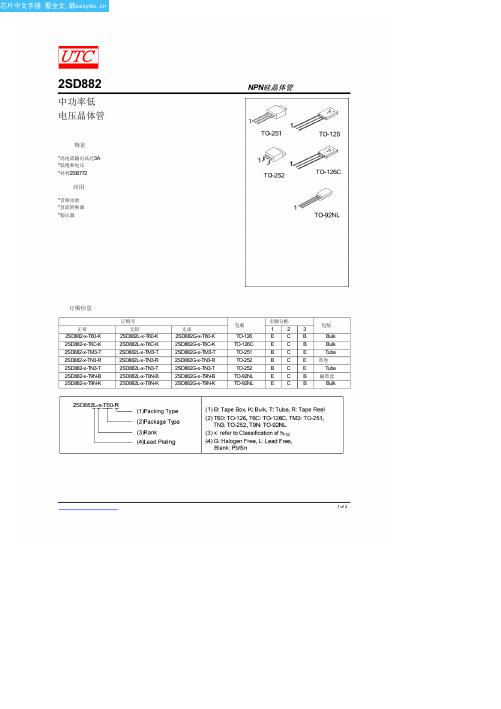
D882中文资料_数据手册_参数
Symbol VCBO VCEO VEBO IC PC
RӨJA
TJ Tstg
Parameter Collector-Base Voltage Collector-Emitter Voltage Emitter-Base Voltage Collector Current -Continuous Collector Power Dissipation Thermal Resistance from Junction to Ambient Junction Temperature Storage Temperature
Dimensions In Millimeters
Min
Max
1.400
1.600
0.320
0.520
0.400
0.580
0.350
0.440
4.400
4.600
1.550 REF.
2.300
2.600
3.940
4.250
1.500 TYP.
3.000 TYP.
0.900
1.200
Dimensions In Inches
O 100-200
Y 160-320
GR 200-400
1
EA,,NJouvn,,22001154
Typical Characteristics
Static Characteristic
2.00
COMMON EMITTER
1.75
10mA 9mA 8mA
T =25 ℃ a
COLLECTOR-EMITTER SATURATION
100
10
1 1
3000 1000
d882二极管参数
d882二极管参数D882二极管是一种广泛应用于电子电路中的晶体管,它具有特定的参数和特性,可以用于控制电流和信号放大等功能。
本文将详细介绍D882二极管的参数及其对电路性能的影响。
一、D882二极管简介D882二极管是一种NPN型的低功耗双极型晶体管,常用作开关和放大电路的组成元件。
它的外形尺寸小巧,结构紧凑,是电子设备中必不可少的一部分。
二、常用参数1. 最大集电极电流(IC max):这是指D882二极管能够承受的最大集电极电流。
当超过这个电流时,会导致晶体管损坏。
2. 最大收集-基极电压(VCBO max):这是指D882二极管集电-基极之间的最大电压值。
超过这个电压值会造成击穿,从而损坏晶体管。
3. 最大发射-基极电压(VEBO max):这是指D882二极管发射-基极之间的最大电压值。
超过这个电压值会造成击穿,同样也会对晶体管产生损害。
4. 最大功耗(Ptot max):这是指D882二极管能够承受的最大功耗。
当超过这个功耗时,会导致晶体管过热,可能发生烧毁。
5. 最大工作温度(Tj max):这是指D882二极管能够耐受的最高工作温度。
超过这个温度范围,晶体管的性能和寿命都会受到影响。
三、参数对电路性能的影响D882二极管的参数对电路性能有着重要的影响。
下面将分别介绍具体的情况。
1. 最大集电极电流(IC max):IC max决定了D882二极管能够承受的最大电流值。
在设计电路时,需要根据所需电流的大小选择合适的二极管,以确保电路的正常工作。
如果超过D882二极管的IC max值,不仅会造成电路异常工作,还会导致二极管损坏。
2. 最大收集-基极电压(VCBO max):VCBO max是指D882二极管集电-基极之间的最大电压值。
如果在使用过程中超过了VCBO max,会引起集电极-基极之间的击穿,导致二极管无法正常工作。
因此,在设计电路时,必须保证电路中的电压值不会超过D882二极管的VCBO max。
D882三极管
【 南京南山半导体有限公司 — 长电三极管选型资料】
【 南京南山半导体有限公司 — 长电三极管选型资料】
Inner Box: 240 mm×165mmer Box
Stamp “EMPTY” on the empty box
= 100μA ,IE= 0 IC IC= = 0 10 mA, IB IE= 100 mA,IC 0 = VCB=40 V, IE 0 = VCE=30 V, IB 0 = = 0 VEB= 6V ,IC VCE= 2V, IC= 1A VCE=2V, IC= 100mA IC= 2A,IB= 0.2A IC= 2A,IB= 0.2A VCE= 5 V,IC=0.1mA f = 10MHz
【 南京南山半导体有限公司 — 长电三极管选型资料】
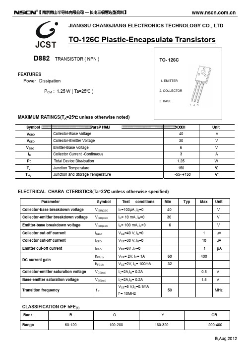
JIANGSU CHANGJIANG ELECTRONICS TECHNOLOGY CO., LTD
TO-126C Plastic-Encapsulate Transistors
D882
TRANSISTOR ( NPN ) TO- 126C
ELECTRICAL CHARA CTERISTICS(Ta=25℃ unless otherwise specified)
Parameter Collector-base breakdown voltage Collector-emitter breakdown voltage Emitter-base breakdown voltage Collector cut-off current Collector cut-off current Emitter cut-off current DC current gain Collector-emitter saturation voltage Base-emitter saturation voltage Transition frequency Symbol V(BR)CBO V(BR)CEO V(BR)EBO ICBO ICEO IEBO hFE(1) hFE(2) VCE(sat) VBE(sat) fT Test conditions Min 40 30 6 1 10 1 60 32 0.5 1.5 50 V V MHz 400 Typ Max Unit V V V μA μA μA
BTD882D3资料

Low Vcesat NPN Epitaxial Planar TransistorBTD882D3Features• Low V CE (sat), V CE (sat)=0.25 V (typical), at I C / I B = 2A / 200mA • Excellent current gain characteristics • Complementary to BTB772D3 • Pb-free packageSymbol OutlineAbsolute Maximum Ratings (Ta=25°C)Parameter Symbol Limits UnitCollector-Base V oltage V CBO 50 VCollector-Emitter V oltage V CEO 50 V Emitter-Base V oltage V EBO 5 V Collector Current (DC) I C 3Collector Current (Pulse) I CP 7 (Note)APower Dissipation (T A =25℃) 1Power Dissipation (T C =25℃) P D 10WJunction Temperature Tj 150 °C Storage TemperatureTstg -55~+150 °CNote : Pulse test, pulse width ≤380µs, duty cycle ≤2%.BTD882D3B :BaseC :Collector E :EmitterCharacteristics (Ta=25°C)Symbol Min. Typ. Max. Unit Test Conditions BV CBO 50 - - V I C =50µA, I E =0 BV CEO 50 - - V I C =1mA, I B =0 BV EBO 5 - - V I E =50µA, I C =0 I CBO - - 1 µA V CB =40V , I E=0 I EBO - - 1 µA V EB =5V , I C =0 *V CE(sat) - 0.25 0.5 V I C =2A, I B =200mA *V BE(sat) - - 2 V I C =2A, I B=200mA *h FE 1 150 - - - V CE =2V , I C =20mA *h FE 2 180 - 820 - V CE =2V , I C =500mA *h FE 3 100 - - - V CE =2V , I C =1A f T - 90 - MHz V CE =5V , I C =100mA, f =100MHz Cob - 45 - pF V CB =10V , f=1MHz*Pulse Test : Pulse Width ≤380µs, Duty Cycle ≤2%Classification Of h FE 2Rank R S T Range 180~390 270~560 390~820Characteristic CurvesTO-126ML Dimension*: TypicalInches Millimeters Inches MillimetersDIMMin. Max. Min. Max. DIMMin. Max. Min. Max.A 0.1356 0.1457 3.44 3.70 H 0.0462 0.0562 1.17 1.42B 0.0170 0.0272 0.43 0.69 I - *0.1795 - *4.56C 0.0344 0.0444 0.87 1.12 J 0.0268 0.0331 0.68 0.84D 0.0501 0.0601 1.27 1.52 K 0.5512 0.5906 14.00 15.00 Φ1 0.1220 0.1299 3.10 3.30 L 0.2903 0.3003 7.37 7.62 Φ2 0.1181 0.1260 3.00 3.20 M 0.1378 0.1478 3.50 3.75 F 0.0737 0.0837 1.87 2.12 N 0.1525 0.1625 3.87 4.12 G 0.0294 0.0494 0.74 1.25 O 0.0740 0.0842 1.88 2.14Notes: 1.Controlling dimension: millimeters. 2.Maximum lead thickness includes lead finish thickness, and minimum lead thickness is the minimum thickness of base material.3.If there is any question with packing specification or packing method, please contact your local CYStek sales office.Material:• Lead: 42 Alloy ; solder plating• Mold Compound: Epoxy resin family, flammability solid burning class: UL94V-0Important Notice:• All rights are reserved. Reproduction in whole or in part is prohibited without the prior written approval of CYStek. • CYStek reserves the right to make changes to its products without notice.• CYStek semiconductor products are not warranted to be suitable for use in Life-Support Applications, or systems.• CYStek assumes no liability for any consequence of customer product design, infringement of patents, or application assistance.Marking:D882。
D882三极管的引脚怎么认?

D882三极管的引脚怎么认?2020年8月14日 09:43 星期五鼠年那个脚是基极,集电极和发射极。
D882三极管正面从左往右,第一个是-E发射极,第二个是-C集电极,第三个是-B基极。
【参数】D882参数:40V,3A,30W,相近代换的有BD785,还可用D883替换,参数是100V,6A,70W 还可以用D1691。
【拓展】三极管,全称应为半导体三极管,也称双极型晶体管、晶体三极管,是一种控制电流的半导体器件其作用是把微弱信号放大成幅度值较大的电信号,也用作无触点开关。
晶体三极管,是半导体基本元器件之一,具有电流放大作用,是电子电路的核心元件。
三极管是在一块半导体基片上制作两个相距很近的PN结,两个PN结把整块半导体分成三部分,中间部分是基区,两侧部分是发射区和集电区,排列方式有PNP和NPN两种。
D882三极管属于NPN排列方式。
三极管D882怎样检测可以用万bai 用表的测试电阻X10档来测试D882的电du阻,黑表zhi笔接1脚(E)、红表笔接2脚(C),(在线)电阻dao约为1KΩ,然后拿一个镊子同时接触1脚和3脚,电阻值有明显的减少即是好管子,如果不动则已损坏。
三极管d882p的引脚是ebc吗一般来说,三极管除了9000系列外,基本上都不是E B C排列,只是9000系列的管子用的很多,所以才给人一种三极管都是E B C排列的错觉。
D882应你是E C B的顺序,你可以万用表测量一下,能找出基极的位置就行。
D882P三极管能用什么替换只要baiPc>10W,VCE>30V,Ic>3A,放大倍数是160-32的NPN硅管都能替du换D882P三极管。
NPN型三极管是一种zhi控制元件,主要用来控制电流的大小,由三dao块半导体构成,其中两块N型和一块P型半导体组成,P型半导体在中间,两块N型半导体在两侧。
三极管是电子电路中最重要的器件,它最主要的功能是电流放大和开关作用。
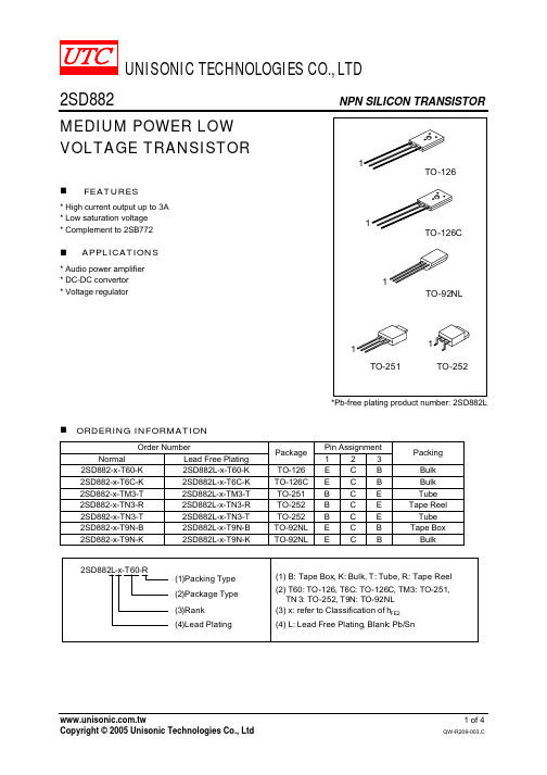
2SD882;中文规格书,Datasheet资料

October 2007Rev 31/82SD882NPN medium power transistorFeatures■High current■Low saturation voltage ■Complement to 2SB772Applications■Voltage regulation ■Relay driver ■Generic switch ■Audio power amplifier ■DC-DC converterDescriptionThe device is a NPN transistor manufactured by using planar technology resulting in rugged high performance devices. The complementary PNP type is 2SB772.Table 1.Device summaryOrder code Marking Package Packing 2SD882D882SOT -32T ubeAbsolute maximum ratings2SD882 1 Absolute maximum ratingsTable 2.Absolute maximum ratingSymbol Parameter Value UnitV CBO Collector-base voltage (I E = 0) 60VV CEO Collector-emitter voltage (I B = 0) 30VV EBO Collector-base voltage (I C = 0) 5VI C Collector current3AI CM Collector peak current (t P < 5ms)6AI B Base current1AI BM Base peak current (t P < 5ms)2AP TOT T otal dissipation at T c = 25°C12.5WT STG Storage temperature-65 to 150°CT J Max. operating junction temperature150°CTable 3.Thermal dataSymbol Parameter Value UnitR thJ-case Thermal resistance junction-case max10°C/W 2/83/82 Electrical characteristics(T CASE = 25°C; unless otherwise specified)Table 4.Electrical characteristicsSymbol ParameterTest conditions Min.Typ.Max.Unit I CES Collector cut-off current(V BE = 0)V CE = 60 V 10µA I CEO Collector cut-off current (I B = 0)V CE = 30 V 100µA I EBOEmitter cut-off current (I C = 0)V EB = 5 V10µAV (BR)CEO(1)Collector-emitter breakdownvoltage (I B = 0 )I C = 10 mA 30VV (BR)CBO Collector-base breakdownvoltage(I E = 0 )I C = 100 µA60VV (BR)EBO Emitter-base breakdownvoltage(I C = 0 )I E = 100 µA5V V CE(sat)(1)Collector-emitter saturationvoltageI C = 1 A I B = 50 mAI C = 2 A I B = 100 mAI C = 3 A I B = 150 mA 0.40.71.1V V V V BE(sat)(1)1.Pulsed duration = 300 ms, duty cycle ≤1.5%.Base-emitter saturation voltage I C = 2 A I B = 100 mA 1.2Vh FE DC current gain I C = 100 mA V CE = 2 V I C = 1 A V CE = 2 V I C = 3 A V CE = 2 V 1008030300f TTransition frequencyI C = 0.1 A V CE = 10 V100MHzcharacteristics (curves) 2.1 Typical4/82SD882Package mechanical data 3 Package mechanical dataIn order to meet environmental requirements, ST offers these devices in ECOPACK®packages. These packages have a Lead-free second level interconnect . The category ofsecond level interconnect is marked on the package and on the inner box label, incompliance with JEDEC Standard JESD97. The maximum ratings related to solderingconditions are also marked on the inner box label. ECOPACK is an ST trademark.ECOPACK specifications are available at: 5/8Package mechanical data2SD8826/82SD882Revision history7/84 Revision historyTable 5.Document revision historyDate RevisionChanges09-Sep-20052Final datasheet. New template 02-Oct-20073Updated mechanical data2SD8828/8Please Read Carefully:Information in this document is provided solely in connection with ST products. STMicroelectronics NV and its subsidiaries (“ST”) reserve the right to make changes, corrections, modifications or improvements, to this document, and the products and services described herein at any time, without notice.All ST products are sold pursuant to ST’s terms and conditions of sale.Purchasers are solely responsible for the choice, selection and use of the ST products and services described herein, and ST assumes no liability whatsoever relating to the choice, selection or use of the ST products and services described herein.No license, express or implied, by estoppel or otherwise, to any intellectual property rights is granted under this document. If any part of this document refers to any third party products or services it shall not be deemed a license grant by ST for the use of such third party products or services, or any intellectual property contained therein or considered as a warranty covering the use in any manner whatsoever of such third party products or services or any intellectual property contained therein.UNLESS O THERWISE SET FO RTH IN ST’S TERMS AND CO NDITIO NS O F SALE ST DISCLAIMS ANY EXPRESS O R IMPLIED WARRANTY WITH RESPECT TO THE USE AND/O R SALE O F ST PRO DUCTS INCLUDING WITHO UT LIMITATIO N IMPLIED WARRANTIES OF MERCHANTABILITY, FITNESS FOR A PARTICULAR PURPOSE (AND THEIR EQUIVALENTS UNDER THE LAWS OF ANY JURISDICTION), OR INFRINGEMENT OF ANY PATENT, COPYRIGHT OR OTHER INTELLECTUAL PROPERTY RIGHT. UNLESS EXPRESSLY APPRO VED IN WRITING BY AN AUTHO RIZED ST REPRESENTATIVE, ST PRO DUCTS ARE NO T RECOMMENDED, AUTHORIZED OR WARRANTED FOR USE IN MILITARY, AIR CRAFT, SPACE, LIFE SAVING, OR LIFE SUSTAINING APPLICATIONS, NOR IN PRODUCTS OR SYSTEMS WHERE FAILURE OR MALFUNCTION MAY RESULT IN PERSONAL INJURY, DEATH, OR SEVERE PROPERTY OR ENVIRONMENTAL DAMAGE. ST PRODUCTS WHICH ARE NOT SPECIFIED AS "AUTOMOTIVE GRADE" MAY ONLY BE USED IN AUTOMOTIVE APPLICATIONS AT USER’S OWN RISK.Resale of ST products with provisions different from the statements and/or technical features set forth in this document shall immediately void any warranty granted by ST for the ST product or service described herein and shall not create or extend in any manner whatsoever, any liability of ST.ST and the ST logo are trademarks or registered trademarks of ST in various countries.Information in this document supersedes and replaces all information previously supplied.The ST logo is a registered trademark of STMicroelectronics. All other names are the property of their respective owners.© 2007 STMicroelectronics - All rights reservedSTMicroelectronics group of companiesAustralia - Belgium - Brazil - Canada - China - Czech Republic - Finland - France - Germany - Hong Kong - India - Israel - Italy - Japan - Malaysia - Malta - Morocco - Singapore - Spain - Sweden - Switzerland - United Kingdom - United States of America分销商库存信息: STM2SD882。
2SD882SQ型号的金属半导体N型NPN功率晶体管说明书
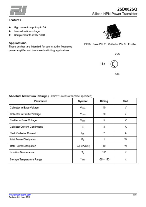
BASE AND COLLECTOR SATURATION VOLTAGE vs. COLLECTOR CURRENT
10
3
1 VBE(sat) 0.6 0.3
0.1 0.06 0.03
0.01 0.006 0.003
VCE(sat)
I C=10.IB Pulse Test
0.001 0.003 0.01 0.03 0.1 0.3 1 3 10
Features.
High current output up to 3A Low saturation voltage Complement to 2SB772SQ
Applications
These devices are intended for use in audio frequency power amplifier and low speed switching applications
at IC = 2 A, IB = 0.2 A
Base Emitter Saturation Voltage
at IC = 2 A, IB = 0.2 A
Gain Bandwidth Product
at VCE = 5 V, IC = 0.1 A
Output Capacitance
at VCB = 10 V, f = 1 MHz
1
µA
-
1
µA
-
0.5
V
-
2
V
90
-
MHz
45
-
pF
h FE-DC Current Gain VBE-Base Emitter Voltage-V
I C-Collector Current-A
D882SS资料

UTC D882SS NPN EPITAXIAL SILICON TRANSISTORUTC UNISONIC TECHNOLOGIES CO. LTD1QW-R206-018,AMEDIUM POWER LOW VOLTAGE TRANSISTORFEATURES*High current output up to 3A*Low saturation voltage *Complement to B772SSAPPLICATIONS* Audio power amplifier * DC-DC convertor * Voltage regulatorMARKING1: EMITTER 2: BASE 3: COLLECTORABSOLUTE MAXIMUM RATINGS ( Ta=25°C ,unless otherwise specified )PARAMETERS SYMBOL RATING UNITCollector-base voltage V CBO 40 VCollector-emitter voltage V CEO 30 V Emitter-base voltage V EBO 5 V Collector dissipation( Tc=25°C) Pc 10 W Collector dissipation( Ta=25°C) Pc 1 W Collector current(DC) Ic 3 A Collector current(PULSE) Ic 7 A Base current I B 0.6 A Junction Temperature T j 150 °C Storage Temperature T STG -55 ~ +150 °CELECTRICAL CHARACTERISTICS (Ta=25°C,unless otherwise specified)PARAMETER SYMBOL TEST CONDITIONS MIN TYP MAXUNIT Collector cut-off current I CBO V CB =30V,I E 0 1000 nA Emitter cut-off current I EBO V EB =3V,Ic 0 1000 nA DC current gain(note 1) h FE1 h FE2 V CE =2V,Ic=20mA V CE =2V,Ic=1A 30 100 200 150 400Collector-emitter saturation voltage V CE (sat) Ic =2A,I B =0.2A 0.3 0.5 V Base-emitter saturation voltage V BE (sat) Ic =2A,I B =0.2A 1.0 2.0 V Current gain bandwidth productf T V CE =5V,Ic =0.1A 80 MHz Output capacitanceCob V CB =10V,I E =0,f =1MHz 45 pFUTC D882SS NPN EPITAXIAL SILICON TRANSISTORUTC UNISONIC TECHNOLOGIES CO. LTD2QW-R206-018,ANote 1:Pulse test:PW<300µs,Duty Cycle<2%CLASSIFICATION OF hFE2RANK Q P E RANGE 100-200 160-320 200-400TYPICAL PARAMETERS PERFORMANCEFig.1 Static characteristics-I c ,C o l l e c t o r c u r r e n t (A )Fig.2 Derating curve of safeoperating areasFig.3 Power DeratingO u t p u t C a p a c i t a n c e (p F )101102103100-Ic,Collector current(mA)-Ic,Collector current(mA)D C c u r r e n t G a i n ,H F E10110210310010101010101010101010UTC D882SS NPN EPITAXIAL SILICON TRANSISTOR UTC UNISONIC TECHNOLOGIES CO. LTD 3QW-R206-018,AUTC D882SS NPN EPITAXIAL SILICON TRANSISTORUTC UNISONIC TECHNOLOGIES CO. LTD 4QW-R206-018,A。
2SD882-E-TN3-R中文资料(Unisonic Technologies)中文数据手册「EasyDatasheet - 矽搜」
0.1m S
集电极电流,I 10
I (最大),脉冲
10
10
10
10
集电极 - 发射极电压
DC电流增益,H
饱和压(MV)
3 of 4
芯片中文手册,看全文,戳
2SD882
典型特征(续)
集电极输出电容
10
I =0
10
f=1MHz
输出电10容(pF)
10
10
10
10
10
集电极基极电压(V)
绝对最大额定值
(TA = 25℃,除非另有规定)
参数 集电极基极电压
集电极 - 发射极电压
发射基电压
集电极电流
基极电流
集电极耗散
(Ta=25℃ )
DC Pulse
TO-92NL TO-251/TO-252/ TO-126/TO-126C
符号
VCBO VCEO VEBO
IC ICP IB
PC
结温 储存温度
NPN硅晶体管
UTC不承担由于使用产品超过,即使是瞬间值,设备故障不承担任何责任,额定数值(例如最大额 定值,工作环境范围或其他参数)任何产品规格和描述或此处包含所有UTC产品上市. UTC产 品并非设计用于生命支持设备,装置或在这些产品故障可合理预期会导致人身伤害系统.严禁复制 全部或部分未经版权拥有者事先书面同意.本文件中不构成任何报价或合同一部分信息,被认为 是准确可靠,恕不另行通知可随时更改.
基地发射极饱和电压 当前增益带宽产品 输出电容
BV CBO BV CEO BV EBO ICBO IEBO hFE1 hFE2 VCE(SAT) VBE(SAT)
fT Cob
注1:脉冲测试:PW300μs,职务循环2%
D882贴片三极管 SOT-89三极管封装D882参数

4.250
1.500 TYP.
3.000 TYP.
0.900
1.200
Dimensions In Inches
Min.
Max.
0.055
0.063
0.013
0.020
0.016
0.023
0.014
0.017
0.173
0.181
0.061 REF.
0.091
0.102
0.155
0.167
0.060 TYP.
Symbol
A b b1 c D D1 E E1 e e1 L
Dimensions In Millimeters
Min.
Max.
1.400
1.600
0.320
0.520
0.400
0.580
0.350
0.440
4.400
4.600
1.550 REF.
2.300
2.600
3.940
75
100
125
150
AMBIENT TEMPERATURE T (℃) a
10 0.1
D882
h —— I
FE
C
T =100℃ a
T =25℃ a
COMMON EMITTER V = 2V
CE
10
100
1000
3000
COLLECTOR CURRENT I (mA) C
V —— I
BEsat
C
T =25℃ a
VOLTAGE V
(mV)
DC CURRENT GAIN h FE
BEsat
1000
100
2SD882L-D-T6C-K中文资料

UNISONIC TECHNOLOGIES CO., LTD2SD882NPN SILICON TRANSISTORMEDIUM POWER LOWVOLTAGE TRANSISTORFEATURES* High current output up to 3A * Low saturation voltage * Complement to 2SB772APPLICATIONS* Audio power amplifier * DC-DC convertor * Voltage regulator*Pb-free plating product number: 2SD882LORDERING INFORMATIONOrder NumberPin AssignmentNormal Lead Free Plating Package 1 2 3 Packing2SD882-x-T60-K 2SD882L-x-T60-K TO-126 E C B Bulk 2SD882-x-T6C-K 2SD882L-x-T6C-K TO-126C E C B Bulk 2SD882-x-TM3-T 2SD882L-x-TM3-T TO-251 B C E Tube 2SD882-x-TN3-R 2SD882L-x-TN3-R TO-252 B C E Tape Reel 2SD882-x-TN3-T 2SD882L-x-TN3-T TO-252 B C E Tube 2SD882-x-T9N-B 2SD882L-x-T9N-B TO-92NL E C B Tape Box 2SD882-x-T9N-K 2SD882L-x-T9N-K TO-92NL E C B BulkABSOLUTE MAXIMUM RATING (Ta=25 , unless otherwise specified )PARAMETER SYMBOL RATINGSUNITCollector-Base Voltage V CBO 40 VCollector-Emitter Voltage V CEO 30 VEmitter-Base Voltage V EBO 5 VDC I C 3 ACollector CurrentPulse I CP 7 ABase Current I B 0.6 ATO-92NL 0.5WCollector Dissipation Ta=25 TO-251/TO-252/TO-126/TO-126C P C1 WJunction Temperature T J +150Storage Temperature T STG-55 ~ +150Note Absolute maximum ratings are those values beyond which the device could be permanently damaged.Absolute maximum ratings are stress ratings only and functional device operation is not implied.ELECTRICAL CHARACTERISTICS (Ta=25℃, unless otherwise specified)PARAMETER SYMBOL TESTCONDITIONSMINTYPMAXUNITCollector-Base Breakdown Voltage BV CBO I C=100µA, I E=0 40 V Collector-Emitter Breakdown Voltage BV CEO I C=1mA, I B=0 30 V Emitter-Base Breakdown Voltage BV EBO I E=100µA, I C=0 5 V Collector Cut-off Current I CBO V CB=30V, I E=01000nA Emitter Cut-off Current I EBO V EB=3V, I C=01000nAh FE1V CE=2V, I C=20mA 30200DC Current Gain (Note 1)h FE2V CE=2V, I C=1A 100150400Collector-Emitter Saturation Voltage V CE(SAT)I C=2A, I B=0.2A0.30.5V Base-Emitter Saturation Voltage V BE(SAT)I C=2A, I B=0.2A1.02.0V Current Gain Bandwidth Product f T V CE=5V, I C=0.1A80MHzOutput Capacitance Cob V CB=10V, I E=0, f=1MHz 45 pFNote 1: Pulse test: PW<300µs, Duty Cycle<2%CLASSIFICATION OF h FE2RANK Q P ERANGE 100-200 160-320 200-400TYPICAL CHARACTERISTICSStatic CharacteristicsCollector -Emitter voltage (V)C o l l e c t o r C u r r e n t , I c (A )00.40.81.21.6Case Temperature , T C (℃)Derating Curve of Safe Operating20015010050-50Current Gain-Bandwidth P roductC u r r e n t G a i n -B a n dw i d t h P r o d u c t , F T (M H z )Collector-Emitter VoltageSafe Operating AreaCollector Current, Ic (A)10310210110010-210-1100101100101102DC Current GainCollector Current, I C (mA)Collector Current, I C (mA)Saturation VoltageD C C u r r e n t G a i n , h F E10101010101010101010101010TYPICAL CHARACTERISTICS(Cont.)Collector Output CapacitanceCollector-Base Voltage (V)O u t p u t C ap a c i t a n c e (p F )10010310210110010-110-210-3。
2SD882L-D-TM3-B中文资料
UNISONIC TECHNOLOGIES CO., LTD2SD882NPN SILICON TRANSISTORMEDIUM POWER LOWVOLTAGE TRANSISTORFEATURES* High current output up to 3A * Low saturation voltage * Complement to 2SB772APPLICATIONS* Audio power amplifier * DC-DC convertor * Voltage regulator*Pb-free plating product number: 2SD882LORDERING INFORMATIONOrder NumberPin AssignmentNormal Lead Free Plating Package 1 2 3 Packing2SD882-x-T60-K 2SD882L-x-T60-K TO-126 E C B Bulk 2SD882-x-T6C-K 2SD882L-x-T6C-K TO-126C E C B Bulk 2SD882-x-TM3-T 2SD882L-x-TM3-T TO-251 B C E Tube 2SD882-x-TN3-R 2SD882L-x-TN3-R TO-252 B C E Tape Reel 2SD882-x-TN3-T 2SD882L-x-TN3-T TO-252 B C E Tube 2SD882-x-T9N-B 2SD882L-x-T9N-B TO-92NL E C B Tape Box 2SD882-x-T9N-K 2SD882L-x-T9N-K TO-92NL E C B BulkABSOLUTE MAXIMUM RATING (Ta=25 , unless otherwise specified )PARAMETER SYMBOL RATINGSUNITCollector-Base Voltage V CBO 40 VCollector-Emitter Voltage V CEO 30 VEmitter-Base Voltage V EBO 5 VDC I C 3 ACollector CurrentPulse I CP 7 ABase Current I B 0.6 ATO-92NL 0.5WCollector Dissipation Ta=25 TO-251/TO-252/TO-126/TO-126C P C1 WJunction Temperature T J +150Storage Temperature T STG-55 ~ +150Note Absolute maximum ratings are those values beyond which the device could be permanently damaged.Absolute maximum ratings are stress ratings only and functional device operation is not implied.ELECTRICAL CHARACTERISTICS (Ta=25℃, unless otherwise specified)PARAMETER SYMBOL TESTCONDITIONSMINTYPMAXUNITCollector-Base Breakdown Voltage BV CBO I C=100µA, I E=0 40 V Collector-Emitter Breakdown Voltage BV CEO I C=1mA, I B=0 30 V Emitter-Base Breakdown Voltage BV EBO I E=100µA, I C=0 5 V Collector Cut-off Current I CBO V CB=30V, I E=01000nA Emitter Cut-off Current I EBO V EB=3V, I C=01000nAh FE1V CE=2V, I C=20mA 30200DC Current Gain (Note 1)h FE2V CE=2V, I C=1A 100150400Collector-Emitter Saturation Voltage V CE(SAT)I C=2A, I B=0.2A0.30.5V Base-Emitter Saturation Voltage V BE(SAT)I C=2A, I B=0.2A1.02.0V Current Gain Bandwidth Product f T V CE=5V, I C=0.1A80MHzOutput Capacitance Cob V CB=10V, I E=0, f=1MHz 45 pFNote 1: Pulse test: PW<300µs, Duty Cycle<2%CLASSIFICATION OF h FE2RANK Q P ERANGE 100-200 160-320 200-400TYPICAL CHARACTERISTICSStatic CharacteristicsCollector -Emitter voltage (V)C o l l e c t o r C u r r e n t , I c (A )00.40.81.21.6Case Temperature , T C (℃)Derating Curve of Safe Operating20015010050-50Current Gain-Bandwidth P roductC u r r e n t G a i n -B a n dw i d t h P r o d u c t , F T (M H z )Collector-Emitter VoltageSafe Operating AreaCollector Current, Ic (A)10310210110010-210-1100101100101102DC Current GainCollector Current, I C (mA)Collector Current, I C (mA)Saturation VoltageD C C u r r e n t G a i n , h F E10101010101010101010101010TYPICAL CHARACTERISTICS(Cont.)Collector Output CapacitanceCollector-Base Voltage (V)O u t p u t C ap a c i t a n c e (p F )10010310210110010-110-210-3。
2SD系列三极管性能资料及代换表

40
102
-
2SD48
富士通
PA
Si.DJ
100
10
3A
20W(Tc=25℃)
175
50
83
-
2SD49
Sony
PA
Si.DJ
100
10
3A
18W(Tc=25℃)
150
50
100
-
2SD50
富士通.日立
PA
Si.DJ
100
10
6A
50W(Tc=25℃)
175
30
102
-
2SD51
Sony
PA
Si.Me
100
6
5A
50W(Tc=25℃)
150
60
102
-
2SD51A
Sony
PA
Si.Me
150
6
5A
50W(Tc=25℃)
150
60
102
-
2SD52
三垦
PA.SW
Si.DJ
100
10
6A
80W(Tc=25℃)
175
20
102
-
2SD53
富士通
PA.SW
Si.DJ
90
12
10A
100W(Tc=25℃)
2SD77
日立
PA
Ge.A
25
12
100
150
85
85
12A
2SB77
2SD77A
日立
PA
Ge.A
45
12
100
150
85
FOSAN富信电子 三极管 D882-产品规格书

安徽富信半导体科技有限公司ANHUI FOSAN SEMICONDUCTOR TECHNOLOGY CO.,LTD.D882SOT-89Bipolar Transistor双极型三极管▉Features特点NPN Low Saturation Voltage低饱和压降▉Absolute Maximum Ratings最大额定值Characteristic特性参数Symbol符号Rat额定值Unit单位Collector-Base Voltage集电极基极电压V CBO40V Collector-Emitter Voltage集电极发射极电压V CEO30V Emitter-Base Voltage发射极基极电压V EBO6V Collector Current集电极电流I C3000mA Power dissipation耗散功率P C(T a=25℃)500mW Thermal Resistance Junction-Ambient热阻RΘJA250℃/WJunction and Storage TemperatureT J,T stg-55to+150℃结温和储藏温度■Device Marking产品打标H FE60-120(R)100-200(O)160-320(Y)200-400(GR)Mark D882ANHUI FOSAN SEMICONDUCTOR TECHNOLOGY CO.,LTD.D882■ElectricalCharacteristics 电特性(T A =25℃unless otherwise noted 如无特殊说明,温度为25℃)Characteristic 特性参数Symbol 符号Min 最小值Type 典型值Max 最大值Unit 单位Collector-Base Breakdown V oltage集电极基极击穿电压(I C =100µA ,I E =0)BV CBO 40——V Collector-Emitter Breakdown Voltage集电极发射极击穿电压(I C =10mA ,I B =0)BV CEO 30——V Emitter-Base Breakdown V oltage发射极基极击穿电压(I E =100µA ,I C =0)BV EBO 6——V Collector-Base Leakage Current集电极基极漏电流(V CB =40V ,I E =0)I CBO ——1µA Collector-Emitter Leakage Current集电极发射极漏电流(V CE =30V ,I B =0)I CEO ——10µA Emitter-Base Leakage Current发射极基极漏电流(V EB =6V ,I C =0)I EBO ——1µADC Current Gain直流电流增益(V CE =2V ,I C =1000mA)H FE60—400Collector-Emitter Saturation Voltage集电极发射极饱和压降(I C =2A ,I B =0.2A)V CE(sat)——0.5VBase-Emitter Saturation V oltage基极发射极饱和压降(I C =2A ,I B =0.2A)V BE(sat)—— 1.5V Transition Frequency特征频率(V CE =5V ,I C =100mA)f T—60—MH ZOutput Capacitance输出电容(V CB =10V ,I E =0,f=1MH Z )C ob—35—pFANHUI FOSAN SEMICONDUCTOR TECHNOLOGY CO.,LTD.D882■Typical Characteristic Curve典型特性曲线ANHUI FOSAN SEMICONDUCTOR TECHNOLOGY CO.,LTD.D882■Dimension外形封装尺寸。
D882 SOT89规格书

0.016
0.023
0.014
0.017
0.173
0.181
0.061 REF.
0.091
0.102
0.155
0.167
0.060 TYP.
0.118 TYP.
0.035
0.047
BEsat
1000
100
10 1
2000 1000
100 1
500
(mV)
CEsat
VOLTAGE V
COLLECTOR-EMITTER SATURATION
100
100
CAPACITANCE C (pF)
=25℃
=100℃
COLLECTOR CURRENT I (mA) C
T a
T a
COLLECTOR POWER DISSIPATION P (mW)
Value
Unit
40
V
30
V
6
V
3
A
0.5
W
150
℃
-55~150
℃
ELECTRICAL CHARACTERISTICS(Ta=25℃ unless otherwise specified)
Parameter Collector-base breakdown voltage Collector-emitter breakdown voltage Emitter-base breakdown voltage Collector cut-off current Collector cut-off current Emitter cut-off current
DC current gain
半导体传感器ADXL288WBRDZ中文规格书

Data SheetADuM1400/ADuM1401/ADuM1402 Rev. L | Page 3 of 31REVISION HISTORY12/2016—Rev. K to Rev. LChanges to Table 1 (4)Changes to Table 2 (6)Changes to Table 3 (9)Changes to Table 4 (11)Changes to Table 5 (13)Changes to Table 6 (15)Changes to Table 7 (17)Changes to Table 9 and Table 10 (19)Changes to Ordering Guide ........................................................... 30 7/2015—Rev. J to Rev. KChanges to Table 9 and Table 10 ................................................... 19 4/2015—Rev. I to Rev. JChanged ADuM140x to ADuM1400/ADuM1401/ADuM1402..................................................................... ThroughoutChanges to Table 10 ........................................................................ 19 4/2014—Rev. H to Rev. IChange to Table 9 ............................................................................ 19 3/2012—Rev. G to Rev. HCreated Hyperlink for Safety and Regulatory ApprovalsEntry in Features Section (1)Change to PC Board Layout Section (27)Updated Outline Dimensions (30)Moved Automotive Products Section ........................................... 31 5/2008—Rev. F to Rev. GAdded ADuM1400W , ADuM1401W , and ADuM1402W Parts ...................................................................................... UniversalAdded Table 4 (11)Added Table 5 (13)Added Table 6 (15)Added Table 7 (17)Changes to Table 12 (20)Changes to Table 13 (21)Added Automotive Products Section (29)Changes to Ordering Guide ........................................................... 30 11/2007—Rev. E to Rev. FChanges to Note 1 (1)Added ADuM140xARW Change vs. Temperature Parameter ... 4 Added ADuM140xARW Change vs. Temperature Parameter (5)Added ADuM140xARW Change vs. Temperature Parameter (8)Changes to Figure 17 ...................................................................... 18 6/2007—Rev. D to Rev. E Updated VDE Certification Throughout ....................................... 1 Changes to Features and Note 1 ...................................................... 1 Changes to Figure 1, Figure 2, and Figure 3 .................................. 1 Changes to Regulatory Information Section ............................... 10 Changes to Table 7 .......................................................................... 11 Added Table 10 ................................................................................ 12 Added Insulation Lifetime Section ............................................... 20 Updated Outline Dimensions........................................................ 21 Changes to Ordering Guide ........................................................... 21 2/2006—Rev. C to Rev. D Updated Format ................................................................. Universal Added TÜV Approval ....................................................... Universal 5/2005—Rev. B to Rev. C Changes to Format ............................................................. Universal Changes to Figure 2 .......................................................................... 1 Changes to Table 3 ............................................................................ 8 Changes to Table 6 .......................................................................... 12 Changes to Ordering Guide ........................................................... 21 6/2004—Rev. A to Rev. B Changes to Format ............................................................. Universal Changes to Features .......................................................................... 1 Changes to Electrical Characteristics—5 V Operation ................ 3 Changes to Electrical Characteristics—3 V Operation ................ 5 Changes to Electrical Characteristics—Mixed 5 V/3 V or 3 V/5 V Operation ............................................................................ 7 Changes to DIN EN 60747-5-2 (VDE 0884 Part 2) Insulation Characteristics Title ........................................................................ 11 Changes to the Ordering Guide .................................................... 19 5/2004—Rev. 0 to Rev. A Updated Format ................................................................. Universal Changes to the Features.................................................................... 1 Changes to Table 7 and Table 8 ..................................................... 14 Changes to Table 9 .......................................................................... 15 Changes to the DC Correctness and Magnetic Field Immunity Section .............................................................................................. 20 Changes to the Power Consumption Section .............................. 21 Changes to the Ordering Guide .................................................... 22 9/2003—Revision 0: Initial VersionADuM1400/ADuM1401/ADuM1402Data SheetRev. L | Page 6 of 31 ELECTRICAL CHARACTERISTICS—3 V, 105°C OPERATION 1 2.7 V ≤ V DD1 ≤ 3.6 V , 2.7 V ≤ V DD2 ≤ 3.6 V; all minimum/maximum specifications apply over the entire recommended operation range, unless otherwise noted; all typical specifications are at T A = 25°C, V DD1 = V DD2 = 3.0 V . These specifications do not apply to ADuM1400W , ADuM1401W , and ADuM1402W automotive grade versions. Table 2.ParameterSymbol Min Typ Max Unit Test Conditions DC SPECIFICATIONSInput Supply Current per Channel, QuiescentI DDI (Q) 0.26 0.31 mA Output Supply Current per Channel, QuiescentI DDO (Q) 0.11 0.14 mA ADuM1400 Total Supply Current, Four Channels 2DC to 2 MbpsV DD1 Supply CurrentI DD1 (Q) 1.2 1.9 mA DC to 1 MHz logic signal freq. V DD2 Supply CurrentI DD2 (Q) 0.5 0.9 mA DC to 1 MHz logic signal freq. 10 Mbps (BRW and CRW Grades Only)V DD1 Supply CurrentI DD1 (10) 4.5 6.5 mA 5 MHz logic signal freq. V DD2 Supply CurrentI DD2 (10) 1.4 2.0 mA 5 MHz logic signal freq. 90 Mbps (CRW Grade Only)V DD1 Supply CurrentI DD1 (90) 37 65 mA 45 MHz logic signal freq. V DD2 Supply CurrentI DD2 (90) 11 15 mA 45 MHz logic signal freq. ADuM1401 Total Supply Current, Four Channels 2DC to 2 MbpsV DD1 Supply CurrentI DD1 (Q) 1.0 1.6 mA DC to 1 MHz logic signal freq. V DD2 Supply CurrentI DD2 (Q) 0.7 1.2 mA DC to 1 MHz logic signal freq. 10 Mbps (BRW and CRW Grades Only)V DD1 Supply CurrentI DD1 (10) 3.7 5.4 mA 5 MHz logic signal freq. V DD2 Supply CurrentI DD2 (10) 2.2 3.0 mA 5 MHz logic signal freq. 90 Mbps (CRW Grade Only)V DD1 Supply CurrentI DD1 (90) 30 52 mA 45 MHz logic signal freq. V DD2 Supply CurrentI DD2 (90) 18 27 mA 45 MHz logic signal freq. ADuM1402 Total Supply Current, Four Channels 2DC to 2 MbpsV DD1 or V DD2 Supply CurrentI DD1 (Q), I DD2 (Q) 0.9 1.5 mA DC to 1 MHz logic signal freq. 10 Mbps (BRW and CRW Grades Only)V DD1 or V DD2 Supply CurrentI DD1 (10), I DD2 (10) 3.0 4.2 mA 5 MHz logic signal freq. 90 Mbps (CRW Grade Only)V DD1 or V DD2 Supply CurrentI DD1 (90), I DD2 (90) 24 39 mA 45 MHz logic signal freq. For All ModelsInput CurrentsI IA , I IB , I IC , I ID , I E1, I E2 −10 +0.01 +10µA 0 V ≤ V IA , V IB , V IC , V ID ≤ V DD1 or V DD2, 0 V ≤ V E1, V E2 ≤ V DD1 or V DD2 Logic High Input ThresholdV IH , V EH 1.6 V Logic Low Input ThresholdV IL , V EL 0.4 V Logic High Output VoltagesV OAH , V OBH , V OCH , V ODH (V DD1 or V DD2) − 0.1 3.0 V I Ox = −20 µA, V Ix = V IxH (V DD1 or V DD2) − 0.4 2.8 V I Ox = −3.2 mA, V Ix = V IxH Logic Low Output Voltages V OAL , V OBL , V OCL , V ODL 0.0 0.1 VI Ox = 20 µA, V Ix = V IxL 0.04 0.1 VI Ox = 400 µA, V Ix = V IxL0.2 0.4 V I Ox = 3.2 mA, V Ix = V IxLSWITCHING SPECIFICATIONSADuM1400ARW /ADuM1401ARW /ADuM1402ARWMinimum Pulse Width 3PW 1000 ns C L = 15 pF, CMOS signal levels Maximum Data Rate 41 Mbps C L = 15 pF, CMOS signal levels Propagation Delay 5t PHL , t PLH 50 75 100 ns C L = 15 pF, CMOS signal levels Pulse Width Distortion, |t PLH − t PHL |5PWD 40 ns C L = 15 pF, CMOS signal levels Change vs. Temperature11 ps/°C C L = 15 pF, CMOS signal levels Propagation Delay Skew 6t PSK50 ns C L = 15 pF, CMOS signal levels Channel-to-Channel Matching 7 t PSKCD /t PSKOD50 ns C L = 15 pF, CMOS signal levels。
SOD882D:无铅封装产品
5H n 0 z 电气 、安装及体 积等特性方面完全兼容其他现有 2引脚或 盒电阻芯 电阻具有 0 n 一5 H的趣低感值,对 5 MH
无引脚 10 装 。 固圃 06封 暖圈
NXP S m ion u t r www.n n p c r e c d cos c .x .o n
具有 的频率 优异 响应. M 小 p/ 热E F 于3V ̄ 届圈■圜 C
2 V C一4WV C 目墨 圈 田 W D 0 D。
s n e t hn og v sh j n 除了低于 2d 5 B的 超 低 噪 声 和 低 于 01 p p mN 的 电 压 Vi hay I t rec ol y ww w. i a  ̄cor
系数 ,这些 电阻还具 有低 至 ±2 p m/ 的绝对 T 5p ℃ CR.
Gl ba Gude o lI I C i
品 总 汇
T 8 M 系列 : 电容器 钽
・
壬l沤 元 件 iL, _ i a4W 0 I i  ̄
Vs a tr c n l y lh yI et h oo 推出新款 T 系列高可靠性 、 n e g M8
表面贴装、具有 2 0 A的超低直流泄露 电流 ( CL 的钽电 0n D )
V s a t r e h ol g i h yI e t c n o y n _ vs a . o i h yc m
L … … … … … …
Hale Waihona Puke 容整 低至 0’ % 根据不 同的外 形尺 寸和特性 .提 供从
WS P 8 50 5 L 0 0 :.W检 流 电阻
Vs a n r c n lg ,n 推出新款表面贴装 P w r ih yIt t h o y Ic ee o o e M tl tp电阻——ws P 8 5 ea r Si L 0 0 该器件采用紧凄的 0 0 85 封装的 05 W检 流电阻. 具有 1 mn ~5 m ̄ 的超 低阻 0 0 !
2SD882P中文资料

The information in this document is subject to change without notice. Before using this document, pleaseconfirm that this is the latest version.Not all products and/or types are available in every country. Please check with an NEC Electronics sales representative for availability and additional information.DATA SHEETDocument No. D17116EJ2V0DS00 (2nd edition)(Previous No. TC-3564)Date Published March 2004 N CP(K) Printed in JapanThe mark shows major revised points.2004DESCRIPTIONThe 2SD882 is NPN silicon transistor suited for the output stage of 3 watts audio amplifier, voltage regulator, DC-DC converter and relay driver.FEATURES• Low saturation voltageV CE(sat) = 0.5 V MAX. (I C = −2 A, I B = 0.2 A) • Excellent h FE linearity and high h FE h FE = 60 to 400 (V CE = 2 V, I C = 1 A)• Less cramping space required due to small and thin package and reducing the trouble for attachment to a radiator. No insulator bushing required.ABSOLUTE MAXIMUM RATINGSMaximum Temperature Storage Temperature −55 to +150°C Junction Temperature 150°C Maximum Maximum Power DissipationsTotal Power Dissipation (T A = 25°Total Power Dissipation (T C = 25°Maximum Voltages and Currents (T A = 25°C) V CBO Collector to Base Voltage 40 V V CEO Collector to Emitter Voltage 30 V V EBO Emitter to Base Voltage 5.0 VI C(DC)Collector Current (DC) 3.0 A I C(pulse)Note Collector Current (pulse) 7.0 ANote Pulse Test PW ≤ 350 µs, Duty Cycle ≤ 2%ELECTRICAL CHARACTERISTICS (T A = 25°C)CHARACTERISTIC SYMBOL TEST CONDITIONSMIN. TYP. MAX. UNITDC Current Gain h FE1 V CE = 2.0 V, I C = 20 mA Note 30 150DC Current Gain h FE2 V CE = 2.0 V, I C = 1.0 A Note60 160 400Gain Bandwidth Product f T V CE = 5.0 V, I C = 0.1 A90 MHz Output Capacitance C ob V CB = 10 V, I E = 0, f = 1.0 MHz 45 pFCollector Cutoff Current I CBO V CB = 30 V, I E = 0 A 1.0 µAEmitter Cutoff Current I EBO V EB = 3.0 V, I C = 0 A1.0µACollector Saturation Voltage V CE(sat) I C = 2.0 A, I B = 0.2 A Note 0.3 0.5 V Base Saturation VoltageV BE(sat)I C = 2.0 A, I B = 0.2 ANote1.02.0 VNote Pulse Test: PW ≤ 350 µs, Duty Cycle ≤ 2%CLASSIFICATION OF h FERank R Q P E Range60 to 120100 to 200160 to 320200 to 400Remark Test Conditions: V CE = 2.0 V, I C = 1.0 APACKAGE DRAWING (Unit: mm)1: Emitter 2: Collector: connected to mounting plane 3: BaseData Sheet D17116EJ2V0DS2TYPICAL CHARACTERISTICS (T A = 25°C)I C = 10 A • I BI E = 0 A (C ob )I C = 0 A (C ib )T AT CV CE I CI CI CV CB V EBV CE V CE = 10 V V CEI C = 1.0 AI C(DC)MAX.T C = 25°CI CI CI C(pulse)50%I Bh F E∆R t hP Th FEV BEV B EC i bC o bC ibC obf TV CE = 5.0 VV BE(sat)V C E(s at )V B E (s a t )V C E (s a t )NoteNoteV C E OThe information in this document is current as of March, 2004. The information is subject to change without notice. For actual design-in, refer to the latest publications of NEC Electronics data sheets or data books, etc., for the most up -to-date sp ecifications of NEC Electronics p roducts. Not all p roducts and/or typ es are available in every country. Please check with an NEC Electronics sales representative for availability and additional information.No part of this d ocument may be copied or reprod uced in any form or by any means without the prior written consent of NEC Electronics. NEC Electronics assumes no responsibility for any errors that may appear in this document.NEC Electronics d oes not assume any liability for infringement of patents, copyrights or other intellectual property rights of third parties by or arising from the use of NEC Electronics products listed in this document or any other liability arising from the use of such prod ucts. No license, express, implied or otherwise, is granted under any patents, copyrights or other intellectual property rights of NEC Electronics or others.Descriptions of circuits, software and other related information in this document are provided for illustrative purposes in semicond uctor prod uct operation and application examples. The incorporation of these circuits, software and information in the d esign of a customer's equipment shall be d one und er the full responsibility of the customer. NEC Electronics assumes no responsibility for any losses incurred by customers or third parties arising from the use of these circuits, software and information.While NEC Electronics end eavors to enhance the quality, reliability and safety of NEC Electronics products, customers agree and acknowled ge that the possibility of d efects thereof cannot be eliminated entirely. To minimize risks of d amage to property or injury (includ ing d eath) to persons arising from d efects in NEC Electronics prod ucts, customers must incorporate sufficient safety measures in their d esign, such as redundancy, fire-containment and anti-failure features.NEC Electronics prod ucts are classified into the following three quality grad es: "Stand ard ", "Special" and "Specific".The "Specific" quality grad e applies only to NEC Electronics prod ucts d eveloped based on a customer-designated "quality assurance program" for a specific application. The recommended applications of an NEC Electronics product depend on its quality grade, as indicated below. Customers must check the quality grade of each NEC Electronics product before using it in a particular application."Standard":Computers, office equipment, communications equipment, test and measurement equipment, audioand visual equipment, home electronic appliances, machine tools, personal electronic equipment and industrial robots."Special":Transportation equipment (automobiles, trains, ships, etc.), traffic control systems, anti-disastersystems, anti-crime systems, safety equipment and medical equipment (not specifically designed for life support)."Specific":Aircraft, aerospace equipment, submersible repeaters, nuclear reactor control systems, lifesupport systems and medical equipment for life support, etc.The quality grad e of NEC Electronics prod ucts is "Stand ard " unless otherwise expressly specified in NEC Electronics data sheets or data books, etc. If customers wish to use NEC Electronics products in applications not intend ed by NEC Electronics, they must contact an NEC Electronics sales representative in ad vance to determine NEC Electronics' willingness to support a given application.(Note)(1)"NEC Electronics" as used in this statement means NEC Electronics Corporation and also includ es itsmajority-owned subsidiaries.(2)"NEC Electronics products" means any product developed or manufactured by or for NEC Electronics (asdefined above).••••••M8E 02. 11-1。
- 1、下载文档前请自行甄别文档内容的完整性,平台不提供额外的编辑、内容补充、找答案等附加服务。
- 2、"仅部分预览"的文档,不可在线预览部分如存在完整性等问题,可反馈申请退款(可完整预览的文档不适用该条件!)。
- 3、如文档侵犯您的权益,请联系客服反馈,我们会尽快为您处理(人工客服工作时间:9:00-18:30)。
UNISONIC TECHNOLOGIES CO., LTD
2SD882
NPN SILICON TRANSISTOR
MEDIUM POWER LOW
VOLTAGE TRANSISTOR
FEATURES
* High current output up to 3A * Low saturation voltage * Complement to 2SB772
APPLICATIONS
* Audio power amplifier * DC-DC convertor * Voltage regulator
*Pb-free plating product number: 2SD882L
ORDERING INFORMATION
Order Number
Pin Assignment
Normal Lead Free Plating Package 1 2 3 Packing
2SD882-x-T60-K 2SD882L-x-T60-K TO-126 E C B Bulk 2SD882-x-T6C-K 2SD882L-x-T6C-K TO-126C E C B Bulk 2SD882-x-TM3-T 2SD882L-x-TM3-T TO-251 B C E Tube 2SD882-x-TN3-R 2SD882L-x-TN3-R TO-252 B C E Tape Reel 2SD882-x-TN3-T 2SD882L-x-TN3-T TO-252 B C E Tube 2SD882-x-T9N-B 2SD882L-x-T9N-B TO-92NL E C B Tape Box 2SD882-x-T9N-K 2SD882L-x-T9N-K TO-92NL E C B Bulk
ABSOLUTE MAXIMUM RATING (Ta=25 , unless otherwise specified )
PARAMETER SYMBOL RATINGS
UNIT
Collector-Base Voltage V CBO 40 V
Collector-Emitter Voltage V CEO 30 V
Emitter-Base Voltage V EBO 5 V
DC I C 3 A
Collector Current
Pulse I CP 7 A
Base Current I B 0.6 A
TO-92NL 0.5
W
Collector Dissipation Ta=25 TO-251/TO-252/
TO-126/TO-126C P C
1 W
Junction Temperature T J +150
Storage Temperature T STG-55 ~ +150
Note Absolute maximum ratings are those values beyond which the device could be permanently damaged.
Absolute maximum ratings are stress ratings only and functional device operation is not implied.
ELECTRICAL CHARACTERISTICS (Ta=25℃, unless otherwise specified)
PARAMETER SYMBOL TEST
CONDITIONS
MIN
TYP
MAX
UNIT
Collector-Base Breakdown Voltage BV CBO I C=100µA, I E=0 40 V Collector-Emitter Breakdown Voltage BV CEO I C=1mA, I B=0 30 V Emitter-Base Breakdown Voltage BV EBO I E=100µA, I C=0 5 V Collector Cut-off Current I CBO V CB=30V, I E=0
1000
nA Emitter Cut-off Current I EBO V EB=3V, I C=0
1000
nA
h FE1V CE=2V, I C=20mA 30
200
DC Current Gain (Note 1)
h FE2V CE=2V, I C=1A 100
150
400
Collector-Emitter Saturation Voltage V CE(SAT)I C=2A, I B=0.2A
0.3
0.5
V Base-Emitter Saturation Voltage V BE(SAT)I C=2A, I B=0.2A
1.0
2.0
V Current Gain Bandwidth Product f T V CE=5V, I C=0.1A
80
MHz
Output Capacitance Cob V CB=10V, I E=0, f=1MHz 45 pF
Note 1: Pulse test: PW<300µs, Duty Cycle<2%
CLASSIFICATION OF h FE2
RANK Q P E
RANGE 100-200 160-320 200-400
TYPICAL CHARACTERISTICS
Static Characteristics
Collector -Emitter voltage (V)
C o l l e c t o r C u r r e n t , I c (A )
00.40.81.21.6Case Temperature , T C (℃)
Derating Curve of Safe Operating
200
15010050
-50
Current Gain-Bandwidth P roduct
C u r r e n t G a i n -B a n d
w i d t h P r o d u c t , F T (M H z )
Collector-Emitter Voltage
Safe Operating Area
Collector Current, Ic (A)
103
102
10110010-2
10-1100101
100
101
102
DC Current Gain
Collector Current, I C (mA)
Collector Current, I C (mA)
Saturation Voltage
D C C u r r e n t G a i n , h F E
101010101010
10
10
10101010
10
TYPICAL CHARACTERISTICS(Cont.)
Collector Output Capacitance
Collector-Base Voltage (V)
O u t p u t C a
p a c i t a n c e (p F )
100
103
10
2
101
100
10-110-210-3。