Power BJT and Diode (I)_Chanho Park
Power Semiconductor Devices and Smart Power ICs

Answers of QuestionsChapter 11-1.P lease classify the power semiconductor discrete devices.A: power rectifiers and power switches.功率整流器和功率开关1-2.P lease list the name of popular power switch.A: power MOSFET, power BJT, IGBT, etc.功率MOS管,功率BJT管,IGBT等1-3.D efine the ideal power semiconductor device.A: It must be able to control the flow of power to loads with ZERO power dissipation.零功耗(包括导通损耗,关断损耗,开关损耗,均为零)1-4.D rawing out the switching waveform of ideal power switch.A:1-5.L ist the device name you known that has the normally-off performance.A: Normally-off: BJT, Enhancement MOSFET, VDMOS, Trench MOS, IGBT,Normally-on: JFET, Depletion MOSFET.1-6.W hich is preferable for normal system, normally-on device or normally-off? Give the reason.A: For normal system, normally-off device is preferable as it has the power dissipation lower than normally-on device’s.常关器件更好。
电力电子术语中英文对照
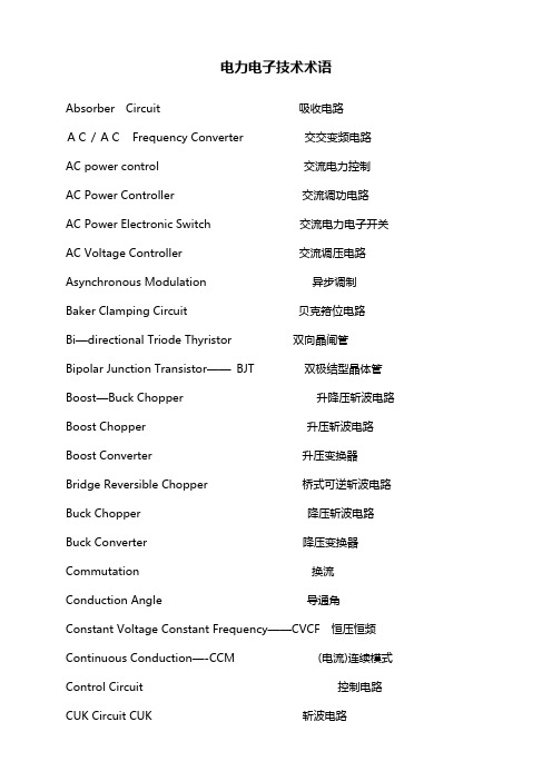
电力电子技术术语Absorber Circuit 吸收电路AC/ACFrequency Converter 交交变频电路AC power control 交流电力控制AC Power Controller 交流调功电路AC Power Electronic Switch 交流电力电子开关AC Voltage Controller 交流调压电路Asynchronous Modulation 异步调制Baker Clamping Circuit 贝克箝位电路Bi—directional Triode Thyristor 双向晶闸管Bipolar Junction Transistor——BJT 双极结型晶体管Boost—Buck Chopper 升降压斩波电路Boost Chopper 升压斩波电路Boost Converter 升压变换器Bridge Reversible Chopper 桥式可逆斩波电路Buck Chopper 降压斩波电路Buck Converter 降压变换器Commutation 换流Conduction Angle 导通角Constant Voltage Constant Frequency——CVCF恒压恒频Continuous Conduction—-CCM (电流)连续模式Control Circuit控制电路CUK Circuit CUK 斩波电路Current Reversible Chopper 电流可逆斩波电路Current Source Type Inverter——CSTI 电流(源)型逆变电路Cycloconvertor 周波变流器DC—AC—DC Converter 直交直电路DC Chopping 直流斩波DC Chopping Circuit直流斩波电路DC—DC Converter 直流-直流变换器Device Commutation 器件换流Direct Current Control 直接电流控制Discontinuous Conduction mode (电流)断续模式Displacement Factor 位移因数Distortion Power 畸变功率Double End Converter 双端电路Driving Circuit 驱动电路Electrical Isolation 电气隔离Fast Acting Fuse 快速熔断器Fast Recovery Diode 快恢复二极管Fast Recovery Epitaxial Diodes 快恢复外延二极管Fast Switching Thyristor 快速晶闸管Field Controlled Thyristor 场控晶闸管Flyback Converter 反激电流Forced Commutation 强迫换流Forward Converter 正激电路Frequency Converter 变频器Full Bridge Converter 全桥电路Full Bridge Rectifier 全桥整流电路Full Wave Rectifier 全波整流电路Fundamental Factor 基波因数Gate Turn-Off Thyristor--GTO可关断晶闸管General Purpose Diode 普通二极管Giant Transistor-—GTR 电力晶体管Half Bridge Converter 半桥电路Hard Switching 硬开关High Voltage IC 高压集成电路Hysteresis Comparison 带环比较方式Indirect Current Control 间接电流控制Indirect DC—DC Converter 直接电流变换电路Insulated-Gate Bipolar Transistor——IGBT 绝缘栅双极晶体管Intelligent Power Module—-IPM 智能功率模块Integrated Gate—Commutated Thyristor—-IGCT集成门极换流晶闸管Inversion 逆变Latching Effect 擎住效应Leakage Inductance 漏感Light Triggered Thyristo---LTT 光控晶闸管Line Commutation 电网换流Load Commutation 负载换流Loop Current 环流元件设备三绕组变压器:three—column transformer ThrClnTrans 双绕组变压器:double-column transformer DblClmnTrans 电容器:Capacitor并联电容器:shunt capacitor电抗器:Reactor母线:Busbar输电线:TransmissionLine发电厂:power plant断路器:Breaker刀闸(隔离开关):Isolator分接头:tap电动机:motor状态参数有功:active power无功:reactive power电流:current容量:capacity电压:voltage档位:tap position有功损耗:reactive loss无功损耗:active loss功率因数:power—factor功率:power功角:power—angle电压等级:voltage grade空载损耗:no—load loss铁损:iron loss铜损:copper loss空载电流:no—load current阻抗:impedance正序阻抗:positive sequence impedance负序阻抗:negative sequence impedance 零序阻抗:zero sequence impedance电阻:resistor电抗:reactance电导:conductance电纳:susceptance无功负载:reactive load 或者QLoad有功负载: active load PLoad遥测:YC(telemetering)遥信:YX励磁电流(转子电流):magnetizing current 定子:stator功角:power—angle上限:upper limit下限:lower limit并列的:apposable高压:high voltage低压:low voltage中压:middle voltage电力系统power system发电机generator励磁excitation励磁器excitor电压voltage电流current母线bus变压器transformer升压变压器step—up transformer高压侧high side输电系统power transmission system输电线transmission line固定串联电容补偿fixed series capacitor compensation 稳定stability电压稳定voltage stability功角稳定angle stability暂态稳定transient stability电厂power plant能量输送power transfer交流AC装机容量installed capacity电网power system落点drop point开关站switch station双回同杆并架double—circuit lines on the same tower 变电站transformer substation补偿度degree of compensation高抗high voltage shunt reactor无功补偿reactive power compensation故障fault调节regulation裕度magin三相故障three phase fault故障切除时间fault clearing time极限切除时间critical clearing time切机generator triping高顶值high limited value强行励磁reinforced excitation线路补偿器LDC(line drop compensation)机端generator terminal静态static (state)动态dynamic (state)单机无穷大系统one machine - infinity bus system 机端电压控制AVR电抗reactance电阻resistance功角power angle有功(功率)active power无功(功率) reactive power功率因数power factor无功电流reactive current下降特性droop characteristics斜率slope额定rating变比ratio参考值reference value电压互感器PT分接头tap下降率droop rate仿真分析simulation analysis传递函数transfer function框图block diagram受端receive—side裕度margin同步synchronization失去同步loss of synchronization 阻尼damping摇摆swing保护断路器circuit breaker电阻:resistance电抗:reactance阻抗:impedance电导:conductance电纳:susceptance导纳:admittance电感:inductance电容:capacitance一般术语电力电子变流器的型式(表1-2)电力电子开关和交流电力电子控制器电力电子设备的基本元件电力电子设备的电路和电路单元电力电子设备的运行电力电子设备的性能电力电子变流器的特性曲线稳定电源。
Power Circuit and Motor-mounted Apparatus Certifie

Power Circuit and Motor-mounted Apparatus Certified for CanadaAccessories, "Inrush Limiter SITOP Series", Model(s) 6EP1967-2AA00 Accessories , Model(s) 6EP4134-3AB00-0AY0, 6EP4134-3AB00-1AY0, 6EP4134-3AB00-2AY0, 6EP4136-3AB00-0AY0, 6EP4136-3AB00-1AY0, 6EP4136-3AB00-2AY0, 6EP4137-3AB00-0AY0, 6EP4137-3AB00-1AY0, 6EP4137-3AB00-2AY0Industrial control equipment, miscellaneous apparatus , Model(s) 6EP1333-1AL12, 6EP1333-3BA00, 6EP1333-3BA00-8AC0, 6EP1334-1AL12, 6EP1334-3BA00, 6EP1334-3BA00-8AB0, 6EP1336-2BA10, 6EP1336-3BA00, 6EP1336-3BA00-8AA0, 6EP1336-3BA10, 6EP1337-3BA00, 6EP1424-3BA00, 6EP1433-0AA00, 6EP1434-2BA10, 6EP1436-2BA10, 6EP1436-3BA00, 6EP1436-3BA00-8AA0, 6EP1436-3BA01, 6EP1436-3BA10, 6EP1437-2BA20, 6EP1437-3BA00, 6EP1437-3BA00-0AA0, 6EP1437-3BA00-8AA0, 6EP1437-3BA10, 6EP1437-3BA20, 6EP1456-2BA00, 6EP1456-3BA00, 6EP1457-3BA00, 6EP1457-3BA00-0AA0, 6EP1961-3BA01, 6EP1962-2BA00, 6EP1964-2BA00Industrial control equipment, miscellaneous apparatus, current monitors , Model(s) 6EP1961-2BA00Industrial control equipment, miscellaneous apparatus, hold-up modules , Model(s) 6EP1961-3BA00Industrial control equipment, miscellaneous apparatus, redundance modules , Model(s) 6EP1961-3BA20, 6EP1961-3BA21Industrial control equipment, miscellaneous apparatus, signaling modules , Model(s) 6EP1961-3BA10Miscellaneous apparatus, power supplies, open type , Model(s) 6EP1311-1SH02, 6EP1311-1SH03, 6EP1311-1SH12, 6EP1311-1SH13, 6EP1321-1SH02, 6EP1321-1SH03, 6EP1321-5BA00, 6EP1322-1SH02, 6EP1322-1SH03, 6EP1322-5BA10, 6EP1331-1SH02, 6EP1331-1SH03, 6EP1331-5BA00, 6EP1331-5BA10, 6EP1332-1SH04, 6EP1332-1SH42, 6EP1332-1SH43, 6EP1332-1SH51, 6EP1332-1SH52, 6EP1332-1SH61, 6EP1332-1SH71, 6EP1332-5BA00, 6EP1332-5BA10, 6EP1332-5BA20, 6EP1351-1SH02, 6EP1351-1SH03, 6EP1352-1SH02, 6EP1352-1SH03, 6EP1536-3AA00Miscellaneous apparatus, Power Supply Accessories, open type , Model(s) 6EP1931-2DC21, 6EP1931-2DC31, 6EP1931-2DC42, 6EP1931-2EC01, 6EP1931-2EC11, 6EP1931-2EC21, 6EP1931-2EC31, 6EP1931-2EC42, 6EP1931-2FC21, 6EP1931-2FC42, 6EP1933-2EC41, 6EP1933-2EC51, 6EP1935-5PG01Power supplies , Model(s) 6EP1321-1LD00, 6EP1332-1LD00Power supplies, open type, "AS-Interface Series", Model(s) 3RX9501-0BA00, 3RX9501-1BA00, 3RX9501-2BA00, 3RX9502-0BA00, 3RX9503-0BA00, 3RX9511-00AA00, 3RX9512-00AA00, 3RX9513-00AA00Power supplies, open type, "SITOP Series", Model(s) 6EP1322-2BA00, 6EP1322-2BA10, 6EP1323-2BA00, 6EP1332-2BA20, 6EP1333-2AA01, 6EP1333-2AA01-0AA0, 6EP1333-2BA01, 6EP1333-2BA20, 6EP1334-2AA01, 6EP1334-2AA01-0AA0, 6EP1334-2AA01-0AB0, 6EP1334-2AA01-0AC0, 6EP1334-2BA01, 6EP1334-2BA20, 6EP1332-1LB00, 6EP1333-1LB00, 6EP1334-1LB00Switch mode power supplies, open type, "SITOP EVS", Model(s) (SITOP EVP 100)6EP1232-1AA10, (SITOP EVP 150)6EP1233-1AA00, (SITOP EVP 300)6EP1234-1AA00, (SITOP EVP 60)6EP1232-1AA00Switch mode power supplies, open type, "SIYOUNG Power", Model(s) (SIYOUNG Power 100)6EP0123-2AAO-0AB0, (SIYOUNG Power 150)6EP0123-3AAO-0AB0, (SIYOUNG Power 300)6EP0123-4AAO-0AB0, (SIYOUNG Power 60)6EP0123-2AAO-0AA0Switching Power Supplies , Model(s) 6EP1322-1LD00, 6EP1331-1LD00, 6EP1332-1LD10, 6EP1333-1LD00, 6EP1334-1LD00NMTR7.E197259Power Circuit and Motor-mounted Apparatus Certified for CanadaPage BottomSee General Information for Power Circuit and Motor-mounted Apparatus Certified for CanadaSIEMENS AGE197259OESTERREICHSIMEAPOSTFACH 83, SIEMENSSTRASSE 901211 VIENNA, AUSTRIALast Updated on 2013-05-20Questions? Print this page Terms of Use Page Top© 2013 UL LLCWhen the UL Leaf Mark is on the product, or when the word "Environment" is included in the UL Mark, please search the UL Environment database for additional information regarding this product's certification.The appearance of a company's name or product in this database does not in itself assure that products so identified have been manufactured under UL's Follow-Up Service. Only those products bearing the UL Mark should be considered to be Certified and covered under UL's Follow-Up Service. Always look for the Mark on the product.UL permits the reproduction of the material contained in the Online Certification Directory subject to the following conditions: 1. The Guide Information, Assemblies, Constructions, Designs, Systems, and/or Certifications (files) must be presented in their entirety and in a non-misleading manner, without any manipulation of the data (or drawings). 2. The statement "Reprinted from the Online Certifications Directory with permission from UL" must appear adjacent to the extracted material. In addition, the reprinted material must include a copyright notice in the following format: "© 2013 UL LLC".。
电力电子器件

3.电路如图所示 VT承受正向门级电压,画出负载R上的电压波
5.判断下列图形中何时灯亮,何时不亮? (1)u2为直流电源,上+下-,S未闭合前灯泡亮不亮? 答:不亮。晶闸管虽具有上+、下-导通的条件,但没有触发 电流,所以不能导通。 (2)u2为直流电源,上+、下-,S闭合后灯泡亮不亮?S闭合 后又断开了,灯泡亮不亮? 答:S闭合后灯泡亮。S闭合后又断开了灯泡照常亮。 (3)u2为直流电源,上-、下+,S未闭合前灯泡亮不亮?S 闭合后又断开了灯泡亮不亮? 答:不亮。u2上-、下+,不具备导通的条件。S闭合也不会亮。
IG2
IG1 IG=0 Ubo +UA
的反相漏电流流过。
当反向电压达到反向击穿电 压后,可能导致晶闸管发热
击穿
损坏。
-IA
• 1.1 使晶闸管导通的条件是什么? 答:使晶闸管导通的条件是:晶闸管承受 正向阳极电压,并在门极注入正向触发电 流。 • 1.2 维持晶闸管导通的条件是什么?怎样 才能使晶闸管由导通变为关断? 答:维持晶闸管导通的条件是使晶闸管的 电流大于能保持晶闸管导通的最小电流 (即维持电流)。 要使晶闸管由导通变为关断,可通过外加 反向阳极电压或减小负载电流的办法,使 流过晶闸管的电流降到维持电流值以下。
UA IA 正向 导通IHOIG2IG1 IG=0 Ubo +UA
随着门极电流幅值的增大, 正向转折电压降低。 晶闸管本身的压降很小, 在1V左右。
击穿
-IA
晶闸管的伏安特性
IG2>IG1>IG
(2)反向特性
反向特性类似二极管的反向 特性。 反向阻断状态时,只有极小
IA 正向 导通
IH UA O
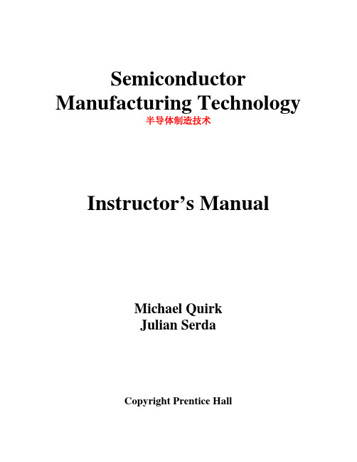
半导体制造技术
Semiconductor Manufacturing Technology半导体制造技术Instructor’s ManualMichael QuirkJulian SerdaCopyright Prentice HallTable of Contents目录OverviewI. Chapter1. Semiconductor industry overview2. Semiconductor materials3. Device technologies—IC families4. Silicon and wafer preparation5. Chemicals in the industry6. Contamination control7. Process metrology8. Process gas controls9. IC fabrication overview10. Oxidation11. Deposition12. Metallization13. Photoresist14. Exposure15. Develop16. Etch17. Ion implant18. Polish19. Test20. Assembly and packagingII. Answers to End-of-Chapter Review QuestionsIII. Test Bank (supplied on diskette)IV. Chapter illustrations, tables, bulleted lists and major topics (supplied on CD-ROM)Notes to Instructors:1)The chapter overview provides a concise summary of the main topics in each chapter.2)The correct answer for each test bank question is highlighted in bold. Test bankquestions are based on the end-of-chapter questions. If a student studies the end-of-chapter questions (which are linked to the italicized words in each chapter), then they will be successful on the test bank questions.2Chapter 1Introduction to the Semiconductor Industry Die:管芯 defective:有缺陷的Development of an Industry•The roots of the electronic industry are based on the vacuum tube and early use of silicon for signal transmission prior to World War II. The first electronic computer, the ENIAC, wasdeveloped at the University of Pennsylvania during World War II.•William Shockley, John Bardeen and Walter Brattain invented the solid-state transistor at Bell Telephone Laboratories on December 16, 1947. The semiconductor industry grew rapidly in the 1950s to commercialize the new transistor technology, with many early pioneers working inSilicon Valley in Northern California.Circuit Integration•The first integrated circuit, or IC, was independently co-invented by Jack Kilby at Texas Instruments and Robert Noyce at Fairchild Semiconductor in 1959. An IC integrates multiple electronic components on one substrate of silicon.•Circuit integration eras are: small scale integration (SSI) with 2 - 50 components, medium scale integration (MSI) with 50 – 5k components, large scale integration (LSI) with 5k to 100kcomponents, very large scale integration (VLSI) with 100k to 1M components, and ultra large scale integration (ULSI) with > 1M components.1IC Fabrication•Chips (or die) are fabricated on a thin slice of silicon, known as a wafer (or substrate). Wafers are fabricated in a facility known as a wafer fab, or simply fab.•The five stages of IC fabrication are:Wafer preparation: silicon is purified and prepared into wafers.Wafer fabrication: microchips are fabricated in a wafer fab by either a merchant chip supplier, captive chip producer, fabless company or foundry.Wafer test: Each individual die is probed and electrically tested to sort for good or bad chips.Assembly and packaging: Each individual die is assembled into its electronic package.Final test: Each packaged IC undergoes final electrical test.•Key semiconductor trends are:Increase in chip performance through reduced critical dimensions (CD), more components per chip (Moore’s law, which predicts the doubling of components every 18-24 months) andreduced power consumption.Increase in chip reliability during usage.Reduction in chip price, with an estimated price reduction of 100 million times for the 50 years prior to 1996.The Electronic Era•The 1950s saw the development of many different types of transistor technology, and lead to the development of the silicon age.•The 1960s were an era of process development to begin the integration of ICs, with many new chip-manufacturing companies.•The 1970s were the era of medium-scale integration and saw increased competition in the industry, the development of the microprocessor and the development of equipment technology. •The 1980s introduced automation into the wafer fab and improvements in manufacturing efficiency and product quality.•The 1990s were the ULSI integration era with the volume production of a wide range of ICs with sub-micron geometries.Career paths•There are a wide range of career paths in semiconductor manufacturing, including technician, engineer and management.2Chapter 2 Characteristics of Semiconductor MaterialsAtomic Structure•The atomic model has three types of particles: neutral neutrons(不带电的中子), positively charged protons(带正电的质子)in the nucleus and negatively charged electrons(带负电的核外电子) that orbit the nucleus. Outermost electrons are in the valence shell, and influence the chemical and physical properties of the atom. Ions form when an atom gains or loses one or more electrons.The Periodic Table•The periodic table lists all known elements. The group number of the periodic table represents the number of valence shell electrons of the element. We are primarily concerned with group numbers IA through VIIIA.•Ionic bonds are formed when valence shell electrons are transferred from the atoms of one element to another. Unstable atoms (e.g., group VIIIA atoms because they lack one electron) easily form ionic bonds.•Covalent bonds have atoms of different elements that share valence shell electrons.3Classifying Materials•There are three difference classes of materials:ConductorsInsulatorsSemiconductors•Conductor materials have low resistance to current flow, such as copper. Insulators have high resistance to current flow. Capacitance is the storage of electrical charge on two conductive plates separated by a dielectric material. The quality of the insulation material between the plates is the dielectric constant. Semiconductor materials can function as either a conductor or insulator.Silicon•Silicon is an elemental semiconductor material because of four valence shell electrons. It occurs in nature as silica and is refined and purified to make wafers.•Pure silicon is intrinsic silicon. The silicon atoms bond together in covalent bonds, which defines many of silicon’s properties. Silicon atoms bond together in set, repeatable patterns, referred to asa crystal.•Germanium was the first semiconductor material used to make chips, but it was soon replaced by silicon. The reasons for this change are:Abundance of siliconHigher melting temperature for wider processing rangeWide temperature range during semiconductor usageNatural growth of silicon dioxide•Silicon dioxide (SiO2) is a high quality, stable electrical insulator material that also serves as a good chemical barrier to protect silicon from external contaminants. The ability to grow stable, thin SiO2 is fundamental to the fabrication of Metal-Oxide-Semiconductor (MOS) devices. •Doping increases silicon conductivity by adding small amounts of other elements. Common dopant elements are from trivalent, p-type Group IIIA (boron) and pentavalent, n-type Group VA (phosphorus, arsenic and antimony).•It is the junction between the n-type and p-type doped regions (referred to as a pn junction) that permit silicon to function as a semiconductor.4Alternative Semiconductor Materials•The alternative semiconductor materials are primarily the compound semiconductors. They are formed from Group IIIA and Group VA (referred to as III-V compounds). An example is gallium arsenide (GaAs).•Some alternative semiconductors come from Group IIA and VIA, referred to as II-VI compounds. •GaAs is the most common III-V compound semiconductor material. GaAs ICs have greater electron mobility, and therefore are faster than ICs made with silicon. GaAs ICs also have higher radiation hardness than silicon, which is better for space and military applications. The primary disadvantage of GaAs is the lack of a natural oxide.5Chapter 3Device TechnologiesCircuit Types•There are two basic types of circuits: analog and digital. Analog circuits have electrical data that varies continuously over a range of voltage, current and power values. Digital circuits have operating signals that vary about two distinct voltage levels – a high and a low.Passive Component Structures•Passive components such as resistors and capacitors conduct electrical current regardless of how the component is connected. IC resistors are a passive component. They can have unwanted resistance known as parasitic resistance. IC capacitor structures can also have unintentional capacitanceActive Component Structures•Active components, such as diodes and transistors can be used to control the direction of current flow. PN junction diodes are formed when there is a region of n-type semiconductor adjacent to a region of p-type semiconductor. A difference in charge at the pn junction creates a depletion region that results in a barrier voltage that must be overcome before a diode can be operated. A bias voltage can be configured to have a reverse bias, with little or no conduction through the diode, or with a forward bias, which permits current flow.•The bipolar junction transistor (BJT) has three electrodes and two pn junctions. A BJT is configured as an npn or pnp transistor and biased for conduction mode. It is a current-amplifying device.6• A schottky diode is formed when metal is brought in contact with a lightly doped n-type semiconductor material. This diode is used in faster and more power efficient BJT circuits.•The field-effect transistor (FET), a voltage-amplifying device, is more compact and power efficient than BJT devices. A thin gate oxide located between the other two electrodes of the transistor insulates the gate on the MOSFET. There are two categories of MOSFETs, nMOS (n-channel) and pMOS (p-channel), each which is defined by its majority current carriers. There is a biasing scheme for operating each type of MOSFET in conduction mode.•For many years, nMOS transistors have been the choice of most IC manufacturers. CMOS, with both nMOS and pMOS transistors in the same IC, has been the most popular device technology since the early 1980s.•BiCMOS technology makes use of the best features of both CMOS and bipolar technology in the same IC device.•Another way to categorize FETs is in terms of enhancement mode and depletion mode. The major different is in the way the channels are doped: enhancement-mode channels are doped opposite in polarity to the source and drain regions, whereas depletion mode channels are doped the same as their respective source and drain regions.Latchup in CMOS Devices•Parasitic transistors can create a latchup condition(???????) in CMOS ICs that causes transistors to unintentionally(无心的) turn on. To control latchup, an epitaxial layer is grown on the wafer surface and an isolation barrier(隔离阻障)is placed between the transistors. An isolation layer can also be buried deep below the transistors.Integrated Circuit Productsz There are a wide range of semiconductor ICs found in electrical and electronic products. This includes the linear IC family, which operates primarily with anal3og circuit applications, and the digital IC family, which includes devices that operate with binary bits of data signals.7Chapter 4Silicon and Wafer Preparation8z Semiconductor-Grade Silicon•The highly refined silicon used for wafer fabrication is termed semiconductor-grade silicon (SGS), and sometimes referred to as electronic-grade silicon. The ultra-high purity of semiconductor-grade silicon is obtained from a multi-step process referred to as the Siemens process.Crystal Structure• A crystal is a solid material with an ordered, 3-dimensional pattern over a long range. This is different from an amorphous material that lacks a repetitive structure.•The unit cell is the most fundamental entity for the long-range order found in crystals. The silicon unit cell is a face-centered cubic diamond structure. Unit cells can be organized in a non-regular arrangement, known as a polycrystal. A monocrystal are neatly arranged unit cells.Crystal Orientation•The orientation of unit cells in a crystal is described by a set of numbers known as Miller indices.The most common crystal planes on a wafer are (100), (110), and (111). Wafers with a (100) crystal plane orientation are most common for MOS devices, whereas (111) is most common for bipolar devices.Monocrystal Silicon Growth•Silicon monocrystal ingots are grown with the Czochralski (CZ) method to achieve the correct crystal orientation and doping. A CZ crystal puller is used to grow the silicon ingots. Chunks of silicon are heated in a crucible in the furnace of the puller, while a perfect silicon crystal seed is used to start the new crystal structure.• A pull process serves to precisely replicate the seed structure. The main parameters during the ingot growth are pull rate and crystal rotation. More homogeneous crystals are achieved with a magnetic field around the silicon melt, known as magnetic CZ.•Dopant material is added to the melt to dope the silicon ingot to the desired electrical resistivity.Impurities are controlled during ingot growth. A float-zone crystal growth method is used toachieve high-purity silicon with lower oxygen content.•Large-diameter ingots are grown today, with a transition underway to produce 300-mm ingot diameters. There are cost benefits for larger diameter wafers, including more die produced on a single wafer.Crystal Defects in Silicon•Crystal defects are interruptions in the repetitive nature of the unit cell. Defect density is the number of defects per square centimeter of wafer surface.•Three general types of crystal defects are: 1) point defects, 2) dislocations, and 3) gross defects.Point defects are vacancies (or voids), interstitial (an atom located in a void) and Frenkel defects, where an atom leaves its lattice site and positions itself in a void. A form of dislocation is astacking fault, which is due to layer stacking errors. Oxygen-induced stacking faults are induced following thermal oxidation. Gross defects are related to the crystal structure (often occurring during crystal growth).Wafer Preparation•The cylindrical, single-crystal ingot undergoes a series of process steps to create wafers, including machining operations, chemical operations, surface polishing and quality checks.•The first wafer preparation steps are the shaping operations: end removal, diameter grinding, and wafer flat or notch. Once these are complete, the ingot undergoes wafer slicing, followed by wafer lapping to remove mechanical damage and an edge contour. Wafer etching is done to chemically remove damage and contamination, followed by polishing. The final steps are cleaning, wafer evaluation and packaging.Quality Measures•Wafer suppliers must produce wafers to stringent quality requirements, including: Physical dimensions: actual dimensions of the wafer (e.g., thickness, etc.).Flatness: linear thickness variation across the wafer.Microroughness: peaks and valleys found on the wafer surface.Oxygen content: excessive oxygen can affect mechanical and electrical properties.Crystal defects: must be minimized for optimum wafer quality.Particles: controlled to minimize yield loss during wafer fabrication.Bulk resistivity(电阻系数): uniform resistivity from doping during crystal growth is critical. Epitaxial Layer•An epitaxial layer (or epi layer) is grown on the wafer surface to achieve the same single crystal structure of the wafer with control over doping type of the epi layer. Epitaxy minimizes latch-up problems as device geometries continue to shrink.Chapter 5Chemicals in Semiconductor FabricationEquipment Service Chase Production BayChemical Supply Room Chemical Distribution Center Holding tank Chemical drumsProcess equipmentControl unit Pump Filter Raised and perforated floorElectronic control cablesSupply air ductDual-wall piping for leak confinement PumpFilterChemical control and leak detection Valve boxes for leak containment Exhaust air ductStates of Matter• Matter in the universe exists in 3 basic states (宇宙万物存在着三种基本形态): solid, liquid andgas. A fourth state is plasma.Properties of Materials• Material properties are the physical and chemical characteristics that describe its unique identity.• Different properties for chemicals in semiconductor manufacturing are: temperature, pressure andvacuum, condensation, vapor pressure, sublimation and deposition, density, surface tension, thermal expansion and stress.Temperature is a measure of how hot or cold a substance is relative to another substance. Pressure is the force exerted per unit area. Vacuum is the removal of gas molecules.Condensation is the process of changing a gas into a liquid. Vaporization is changing a liquidinto a gas.Vapor pressure is the pressure exerted by a vapor in a closed container at equilibrium.Sublimation is the process of changing a solid directly into a gas. Deposition is changing a gas into a solid.Density is the mass of a substance divided by its volume.Surface tension of a liquid is the energy required to increase the surface area of contact.Thermal expansion is the increase in an object’s dimension due to heating.Stress occurs when an object is exposed to a force.Process Chemicals•Semiconductor manufacturing requires extensive chemicals.• A chemical solution is a chemical mixture. The solvent is the component of the solution present in larger amount. The dissolved substances are the solutes.•Acids are solutions that contain hydrogen and dissociate in water to yield hydronium ions. A base is a substance that contains the OH chemical group and dissociates in water to yield the hydroxide ion, OH-.•The pH scale is used to assess the strength of a solution as an acid or base. The pH scale varies from 0 to 14, with 7 being the neutral point. Acids have pH below 7 and bases have pH values above 7.• A solvent is a substance capable of dissolving another substance to form a solution.• A bulk chemical distribution (BCD) system is often used to deliver liquid chemicals to the process tools. Some chemicals are not suitable for BCD and instead use point-of-use (POU) delivery, which means they are stored and used at the process station.•Gases are generally categorized as bulk gases or specialty gases. Bulk gases are the relatively simple gases to manufacture and are traditionally oxygen, nitrogen, hydrogen, helium and argon.The specialty gases, or process gases, are other important gases used in a wafer fab, and usually supplied in low volume.•Specialty gases are usually transported to the fab in metal cylinders.•The local gas distribution system requires a gas purge to flush out undesirable residual gas. Gas delivery systems have special piping and connections systems. A gas stick controls the incoming gas at the process tool.•Specialty gases may be classified as hydrides, fluorinated compounds or acid gases.Chapter 6Contamination Control in Wafer FabsIntroduction•Modern semiconductor manufacturing is performed in a cleanroom, isolated from the outside environment and contaminants.Types of contamination•Cleanroom contamination has five categories: particles, metallic impurities, organic contamination, native oxides and electrostatic discharge. Killer defects are those causes of failure where the chip fails during electrical test.Particles: objects that adhere to a wafer surface and cause yield loss. A particle is a killer defect if it is greater than one-half the minimum device feature size.Metallic impurities: the alkali metals found in common chemicals. Metallic ions are highly mobile and referred to as mobile ionic contaminants (MICs).Organic contamination: contains carbon, such as lubricants and bacteria.Native oxides: thin layer of oxide growth on the wafer surface due to exposure to air.Electrostatic discharge (ESD): uncontrolled transfer of static charge that can damage the microchip.Sources and Control of Contamination•The sources of contamination in a wafer fab are: air, humans, facility, water, process chemicals, process gases and production equipment.Air: class number designates the air quality inside a cleanroom by defining the particle size and density.Humans: a human is a particle generator. Humans wear a cleanroom garment and follow cleanroom protocol to minimize contamination.Facility: the layout is generally done as a ballroom (open space) or bay and chase design.Laminar airflow with air filtering is used to minimize particles. Electrostatic discharge iscontrolled by static-dissipative materials, grounding and air ionization.Ultrapure deiniozed (DI) water: Unacceptable contaminants are removed from DI water through filtration to maintain a resistivity of 18 megohm-cm. The zeta potential represents a charge on fine particles in water, which are trapped by a special filter. UV lamps are used for bacterial sterilization.Process chemicals: filtered to be free of contamination, either by particle filtration, microfiltration (membrane filter), ultrafiltration and reverse osmosis (or hyperfiltration).Process gases: filtered to achieve ultraclean gas.Production equipment: a significant source of particles in a fab.Workstation design: a common layout is bulkhead equipment, where the major equipment is located behind the production bay in the service chase. Wafer handling is done with robotic wafer handlers. A minienvironment is a localized environment where wafers are transferred on a pod and isolated from contamination.Wafer Wet Cleaning•The predominant wafer surface cleaning process is with wet chemistry. The industry standard wet-clean process is the RCA clean, consisting of standard clean 1 (SC-1) and standard clean 2 (SC-2).•SC-1 is a mixture of ammonium hydroxide, hydrogen peroxide and DI water and capable of removing particles and organic materials. For particles, removal is primarily through oxidation of the particle or electric repulsion.•SC-2 is a mixture of hydrochloric acid, hydrogen peroxide and DI water and used to remove metals from the wafer surface.•RCA clean has been modified with diluted cleaning chemistries. The piranha cleaning mixture combines sulfuric acid and hydrogen peroxide to remove organic and metallic impurities. Many cleaning steps include an HF last step to remove native oxide.•Megasonics(兆声清洗) is widely used for wet cleaning. It has ultrasonic energy with frequencies near 1 MHz. Spray cleaning will spray wet-cleaning chemicals onto the wafer. Scrubbing is an effective method for removing particles from the wafer surface.•Wafer rinse is done with overflow rinse, dump rinse and spray rinse. Wafer drying is done with spin dryer or IPA(异丙醇) vapor dry (isopropyl alcohol).•Some alternatives to RCA clean are dry cleaning, such as with plasma-based cleaning, ozone and cryogenic aerosol cleaning.Chapter 7Metrology and Defect InspectionIC Metrology•In a wafer fab, metrology refers to the techniques and procedures for determining physical and electrical properties of the wafer.•In-process data has traditionally been collected on monitor wafers. Measurement equipment is either stand-alone or integrated.•Yield is the percent of good parts produced out of the total group of parts started. It is an indicator of the health of the fabrication process.Quality Measures•Semiconductor quality measures define the requirements for specific aspects of wafer fabrication to ensure acceptable device performance.•Film thickness is generally divided into the measurement of opaque film or transparent film. Sheet resistance measured with a four-point probe is a common method of measuring opaque films (e.g., metal film). A contour map shows sheet resistance deviations across the wafer surface.•Ellipsometry is a nondestructive, noncontact measurement technique for transparent films. It works based on linearly polarized light that reflects off the sample and is elliptically polarized.•Reflectometry is used to measure a film thickness based on how light reflects off the top and bottom surface of the film layer. X-ray and photoacoustic technology are also used to measure film thickness.•Film stress is measured by analyzing changes in the radius of curvature of the wafer. Variations in the refractive index are used to highlight contamination in the film.•Dopant concentration is traditionally measured with a four-point probe. The latest technology is the thermal-wave system, which measures the lattice damage in the implanted wafer after ion implantation. Another method for measuring dopant concentration is spreading resistance probe. •Brightfield detection is the traditional light source for microscope equipment. An optical microscope uses light reflection to detect surface defects. Darkfield detection examines light scattered off defects on the wafer surface. Light scattering uses darkfield detection to detectsurface particles by illuminating the surface with laser light and then using optical imaging.•Critical dimensions (CDs) are measured to achieve precise control over feature size dimensions.The scanning electron microscope is often used to measure CDs.•Conformal step coverage is measured with a surface profiler that has a stylus tip.•Overlay registration measures the ability to accurately print photoresist patterns over a previously etched pattern.•Capacitance-voltage (C-V) test is used to verify acceptable charge conditions and cleanliness at the gate structure in a MOS device.Analytical Equipment•The secondary-ion mass spectrometry (SIMS) is a method of eroding a wafer surface with accelerated ions in a magnetic field to analyze the surface material composition.•The atomic force microscope (AFM) is a surface profiler that scans a small, counterbalanced tip probe over the wafer to create a 3-D surface map.•Auger electron spectroscopy (AES) measures composition on the wafer surface by measuring the energy of the auger electrons. It identifies elements to a depth of about 2 nm. Another instrument used to identify surface chemical species is X-ray photoelectron spectroscopy (XPS).•Transmission electron microscopy (TEM) uses a beam of electrons that is transmitted through a thin slice of the wafer. It is capable of quantifying very small features on a wafer, such as silicon crystal point defects.•Energy-dispersive spectrometer (EDX) is a widely used X-ray detection method for identifying elements. It is often used in conjunction with the SEM.• A focused ion beam (FIB) system is a destructive technique that focuses a beam of ions on the wafer to carve a thin cross section from any wafer area. This permits analysis of the wafermaterial.Chapter 8Gas Control in Process ChambersEtch process chambers••The process chamber is a controlled vacuum environment where intended chemical reactions take place under controlled conditions. Process chambers are often configured as a cluster tool. Vacuum•Vacuum ranges are low (rough) vacuum, medium vacuum, high vacuum and ultrahigh vacuum (UHV). When pressure is lowered in a vacuum, the mean free path(平均自由行程) increases, which is important for how gases flow through the system and for creating a plasma.Vacuum Pumps•Roughing pumps are used to achieve a low to medium vacuum and to exhaust a high vacuum pump. High vacuum pumps achieve a high to ultrahigh vacuum.•Roughing pumps are dry mechanical pumps or a blower pump (also referred to as a booster). Two common high vacuum pumps are a turbomolecular (turbo) pump and cryopump. The turbo pump is a reliable, clean pump that works on the principle of mechanical compression. The cryopump isa capture pump that removes gases from the process chamber by freezing them.。
2.Devices
* commutation states (dynamic)
di/dt rating – turn-on
Real Characteristics for the actual circuit design
a hot point in the region where the first conduction occurs
Power Devices
iG I GT
t
iA
t
v AK
v
GK
t
t
Power Devices
GTOs Ratings Switching frequency up to up to 4500V, 3000A 10 kHz
• Slow switching speeds
• Used at very high power levels • Require elaborate gate control circuitry
Power Devices
Safe Operating Area of Power Transistors
Power Devices
Power Transistors Ratings Switching frequency
up to up to
1400V, 400A 10 kHz
• Complicated base control - high switching loss
P-N-P Transistor. (a) Structure. (b) Symbol.
Idealized Switch Characteristics
Power Devices
Power Transistors
Profile of the base to the collector current — base current just sufficient to maintain saturation if too small amplification -VCE high, second breakdown! ? if too large ? deep saturation–turn-off too slow!
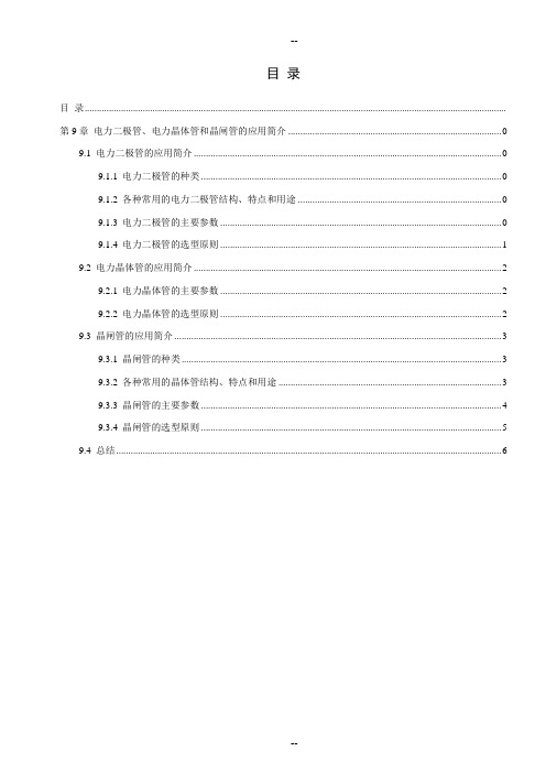
第9章--电力二极管、电力晶体管和晶闸管的应用简介
目录目录.............................................................................................................................................................................. 第9章电力二极管、电力晶体管和晶闸管的应用简介 . 09.1 电力二极管的应用简介 09.1.1 电力二极管的种类 09.1.2 各种常用的电力二极管结构、特点和用途 09.1.3 电力二极管的主要参数 09.1.4 电力二极管的选型原则 (1)9.2 电力晶体管的应用简介 (2)9.2.1 电力晶体管的主要参数 (2)9.2.2 电力晶体管的选型原则 (2)9.3 晶闸管的应用简介 (3)9.3.1 晶闸管的种类 (3)9.3.2 各种常用的晶体管结构、特点和用途 (3)9.3.3 晶闸管的主要参数 (4)9.3.4 晶闸管的选型原则 (5)9.4 总结 (6)第9章电力二极管、电力晶体管和晶闸管的应用简介9.1 电力二极管的应用简介电力二极管(Power Diode)在20世纪50年代初期就获得应用,当时也被称为半导体整流器;它的基本结构和工作原理与信息电子电路中的二极管相同,都以半导体PN结为基础,实现正向导通、反向截止的功能。
电力二极管是不可控器件,其导通和关断完全是由其在主电路中承受的电压和电流决定的。
电力二极管实际上是由一个面积较大的PN结和两端引线以及封装组成的。
9.1.1 电力二极管的种类电力二极管主要有普通二极管、快速恢复二极管和肖特基二极管。
9.1.2 各种常用的电力二极管结构、特点和用途名称结构特点、用途实例图片整流二极管多用于开关频率不高(1kHz以下)的整流电路中。
其反向恢复时间较长,一般在5s以上,其正向电流定额和反向电压定额可以达到很高。
电力电子术语中英文对照

电力电子技术术语Absorber CircuitAC/AC Freque ncy Conv erter AC power con trolAC Power Con trollerAC Power Electro nic SwitchAC Voltage Co ntroller Asynchronous Modulati onBaker Clamp ing CircuitBi-direct ional Triode Thyristor Bipolar Junction Tran sistor-- BJT Boost-Buck ChopperBoost ChopperBoost Conv erterBridge Reversible ChopperBuck ChopperBuck Conv erterCommutatio nCon duct ion An gleCon sta nt Voltage Con sta nt Freque ncy-Contin uous Con ductio n--CCM Control Circuit吸收电路交交变频电路交流电力控制交流调功电路交流电力电子开关交流调压电路异步调制9贝克箝位电路双向晶闸管双极结型晶体管升降压斩波电路升压斩波电路升压变换器桥式可逆斩波电路降压斩波电路降压变换器换流导通角CVCF 恒压恒频(电流)连续模式控制电路CUK Circuit CUK 斩波电路Curre nt Reversible Chopper 电流可逆斩波电路Curre nt Source Type In verter--CSTI 电流(源)型逆变电路Cycloc on vertor 周波变流器DC-AC-DC Co nverter 直交直电路DC Choppi ng 直流斩波DC Choppi ng Circuit 直流斩波电路DC-DC Con verter 直流-直流变换器Device Commutati on 器件换流Direct Current Con trol 直接电流控制Disc ontinu ous Con duct ion mode (电流)断续模式Displaceme nt Factor 位移因数Distortio n Power 畸变功率Double End Conv erter 双端电路Drivi ng Circuit 驱动电路Electrical Isolati on 电气隔离Fast Acting Fuse 快速熔断器Fast Recovery Diode 快恢复二极管Fast Recovery Epitaxial Diodes 快恢复外延二极管Fast Switch ing Thyristor 快速晶闸管Field Con trolled Thyristor 场控晶闸管Flyback Conv erter 反激电流Forced Commutati on 强迫换流Freque ncy Conv erter 变频器 Full Bridge Conv erter 全桥电路 Full Bridge Rectifier 全桥整流电路 Full Wave Rectifier 全波整流电路 Fun dame ntal Factor 基波因数 Gate Turn-Off Thyristor--GTO 可关断晶闸管 Gen eral Purpose Diode 普通二极管 Gia nt Tran sistor--GTR 电力晶体管 Half Bridge Conv erter 半桥电路 Hard Switchi ng 硬开关 High Voltage IC 高压集成电路 Hysteresis Comparis on 带环比较方式 In direct Curre nt Con trol 间接电流控制 In direct DC-DC Co nverter直接电流变换电路 In sulated-Gate Bipolar Tran sistor--IGBT 绝缘栅双极晶体管 Intelligent Power Module--IPM智能功率模块Forward Con verter正激电路 In tegrated Gate-Commutated Thyristor--IGCT 集成门极换流晶闸管 In versi on 逆变 Latch ing Effect 擎住效应 Leakage In ducta nee 漏感 Light Triggered Thyristo---LTT 光控晶闸管 Li ne Commutati on电网换流Load Commutati on Loop Curre nt元件设备三绕组变压器:three-colu mn tran sformer ThrCI nTrans 双绕组变压器: double-colu mn tran sformer DbICI mnTrans 电容器:Capacitor并联电容器:shunt capacitor 电抗器:Reactor 母线:Busbar 输电线: Tran smissi onLine 发电厂: power pla nt 断路器: Breaker刀闸(隔离开关):Isolator 分接头:tap 电动机:motor状态参数有功:active power 无功:reactive power 电流:current 容量:capacity 电压:voltage 档位:tap position有功损耗:reactive loss 无功损耗:active loss负载换流 环流功率因数:power-factor功率:power功角:power-angle电压等级:voltage grade空载损耗:n o-load loss铁损:iron loss铜损:copper loss空载电流:no-load curre nt阻抗:impedanee正序阻抗:positive seque nee impeda nee 负序阻抗:n egative seque nee impeda nee 零序阻抗:zero seque nee impeda nee 电阻:resistor电抗:reaetanee电导:eonduetanee电纟内:suseeptanee无功负载:reactive load 或者QLoad有功负载:active load PLoad遥测:YC(telemetering)遥信:YX励磁电流(转子电流):magnetizing eurrent 定子:stator功角:power-angle上限:upper limit下限:lower limit并歹U的:apposable高压:high voltage低压:low voltage中压:middle voltage电力系统power system发电机generator励磁excitation励磁器excitor电压voltage电流current母线bus变压器transformer升压变压器step-up transformer高压侧high side输电系统power transmission system输电线transmission line固定串联电容补偿fixed series capacitor compensation 稳定stability电压稳定voltage stability功角稳定angle stability暂态稳定transient stability电厂power plant能量输送power transfer交流AC装机容量in stalled capacity电网power system落点drop point开关站switch station双回同杆并架double-circuit lines on the same tower 变电站transformer substation补偿度degree of compensation高抗high voltage shunt reactor无功补偿reactive power compensation故障fault调节regulation裕度magin三相故障three phase fault故障切除时间fault clearing time极限切除时间critical cleari ng time切机generator triping高顶值high limited value强行励磁reinforced excitation线路补偿器LDC(line drop compensation)机端generator terminal静态static (state)动态dynamic (state)单机无穷大系统one mach ine - infin ity bus system 机端电压控制AVR电抗reactanee电阻resista nee功角power angle有功(功率) active power无功(功率) reactive power功率因数power factor无功电流reactive current下降特性droop characteristics斜率slope额定rati ng变比ratio参考值referenee value电压互感器PT分接头tap下降率droop rate仿真分析simulation analysis传递函数transfer function框图block diagram受端receive-side裕度margin同步synchronization失去同步loss of synchronization 阻尼damping摇摆swing保护断路器circuit breaker电阻:resista nee电抗:reacta nee阻抗:impeda nee电导:con ducta nee电纳:suscepta nee导纳:admitta nee电感:in ducta nee电容:capacita nee一般术语稳定电源。
关于HV CMOS
关于HV CMOS和DMOS的困惑alchemist 发表于: 2009-5-19 23:03 来源: 半导体技术天地一直很困惑:一般foundry对于高压器件有两条路线,1)HV CMOS工艺,一般用Double Diffusion,一般能到30V,再高就不行了;2)BCD工艺,高压一般用DMOS,一般20V、40V,更高电压也有。
所谓存在的就是合理的,这两种技术能同时并存并且齐头并进的发展,肯定有它们各自的优势和适合的应用,有没有高手能解释比较一下!我的理解(猜的):1)HVCMOS采用的是对称的结构(当然也可以有非对称管),Vgs和Vds基本相当,电路设计不受限制,应用上灵活,管子特性比较好,IV curve的形状和低压的MOS管没太大的差别;但需要额外增加较多的mask和工艺环节,同时最高电压有上限,32V顶天了。
2)DMOS采用非对称结构,Vgs远小于Vds,电路设计受限制,管子特性应该没有HVMOS 的好;电压可以很高,Vds 60V、100V都不成问题,增加的mask应该比HVCMOS工艺的少。
不知道猜得对不对,请明白人澄清一下,谢谢!最新回复求HVCMOS和DMOS区别?提问者:周镇义2013-12-06满意回答DMOS的特性在於low Rdson,用於power managerment ICHV CMOS 主用於 driver IC高压mos有两种常用的实现方式1、是用井来做轻参杂,提供高耐压的漂移区。
工艺可以完全做到和cmos 一样8 ^" [; T' X3 }- {* e比如HVNOMS,用N井在Drain端,作为漂移区,就好了。
耐压也可以做到很高40V没有问题96 d; [: r*上面有场氧和多晶2、就是DMOS,有LDMOS,VDMOS还有DD结构做的。
DD结构最简单,又分单边和双边DD。
LDMOS和VDmos没有什么好说的。
但是要做到扩散长度的差异,必然退火要讲究了。
powerbi calculate 布尔表达式 度量值

powerbi calculate 布尔表达式度量值1.引言1.1 概述PowerBI是一款强大的商业智能工具,用于分析和可视化大量数据,帮助用户做出准确的决策。
在PowerBI中,Calculate函数是其中一个重要的函数,它允许用户根据特定的条件来计算度量值。
而布尔表达式作为Calculate函数的参数之一,用于判断某个条件是否成立。
本文将深入探讨PowerBI中Calculate函数与布尔表达式的关系,并研究它们在度量值计算中的应用。
我们将从PowerBI的简介开始,介绍它的基本概念和功能,然后重点讨论Calculate函数的定义和使用方法。
接着,我们将详细解释布尔表达式的概念,并探讨它与Calculate函数的结合使用。
最后,我们将总结本文的主要内容,并探讨PowerBI应用中的一些启示。
通过阅读本文,读者将了解到PowerBI中Calculate函数与布尔表达式的基本概念和作用,以及它们在度量值计算中的实际应用。
本文的目标是帮助读者更好地理解和运用PowerBI的Calculate函数,提升数据分析和可视化的能力,为业务决策提供有力的支持。
文章结构部分的内容可以写成如下形式:1.2 文章结构本文将按照以下结构进行分析和讨论:第一部分是引言部分,主要介绍文章的概述、结构和目的。
在这一部分中,我们将简要介绍PowerBI的背景和Calculate函数的概念,并说明本文的主要目的是探讨如何在PowerBI中使用布尔表达式来进行度量值的计算。
第二部分是正文部分,将分为几个小节来详细讨论相关内容。
首先,我们将介绍PowerBI的简介,包括其定义、特点和应用场景。
然后,我们将深入了解Calculate函数的概念,包括其基本语法和用法。
接下来,我们将介绍布尔表达式的定义,并阐述其在PowerBI中的重要性和作用。
我们将探讨如何构建和使用布尔表达式来进行数据过滤和逻辑计算。
然后,我们将详细介绍如何在Calculate函数中使用布尔表达式来进行度量值的计算。
电气英语大全

盛年不重来,一日难再晨。
及时宜自勉,岁月不待人three-colu mn tran sformer ThrCInTrans三绕组变压器:双绕组变压器:double-colu mn tran sformer DblCl mnTrans电容器:Capacitor 并联电容器:shunt capacitor 电抗器:Reactor母线:Busbar 输电线:TransmissionLine 发电厂:power pla nt断路器:Breaker刀闸(隔离开关):Isolator分接头:tap 电动机:motor 有功:active power 无功:reactive power 电流:current 容量:capacity 电压:voltage档位:tap position 有功损耗:reactive loss 无功损耗:active loss功率因数:power-factor 功率:power 功角:power-angle 电压等级:voltage grade 空载损耗:no-load loss 铁损:ironloss铜损:copper loss 空载电流:no-load current 阻抗:impeda nee正序阻抗:positive seque nee impeda nee 负序阻抗: n egative seque nee impeda neeabscissa axis 横坐标ae motor 交流环电动机active (passive) eireuit eleme nts 有(无)源电路元件aetive comp onent 有功分量active in respeet to 相对….呈阻性admitta nee 导纟纳air-gap flux distributi on 气隙磁通分布air-gap flux 气隙磁通air-gap line 气隙磁化线algebraic 代数的algorithmic 算法的alloy合金ampere-turns 安匝(数)amplidy ne 微场扩流发电机Amplitude Modulatio n(AM 调幅armature circuit 电枢电路armature coil 电枢线圈armature m.m.f. wave 电枢磁势波atte nu ate 衰减automatic stati on 无人值守电站automatic Voltage regulator(AVR) 自动电压调整器auxiliary motor 辅助电动机ban dwidth 带宽base基极bilateral circuit 双向电路bimotored 双马达的biphase 双相的bipolar jun ctio n tran sistor (BJT) 双极性晶体管共享知识分享快乐block diagram 方框图boost 增压boost-buck 升压去磁breakaway force 起步阻力breakdow n torque 极限转矩bronze 青铜buck补偿capacita nee effect 电容效应carb on-filame nt lamp 碳丝灯泡carrier 载波Cartesian coord inates 笛卡儿坐标系cast-alu minum rotor 铸铝转子chopper circuit 斩波电路circuit bra nch 支路circuit comp onents 电路元件circuit diagram 电路图circuit parameters 电路参数coaxial共轴的,同轴的coil wi ndi ng 线圈绕组coin cide in phase with 与….同相collector 集电极commutatio n con diti on 换向状况commutator-brush comb in ati on 换向器-电刷总线complex impeda nee 复数阻抗complex number复数compo und gen erator 复励发电机compo un ded 复励con ducta nee 电导con ductor 导体corridor 通路coupli ng capacitor 结合电容cumulatively compo un ded motor dc gen erator直流发电机dc motor 直流电动机 de machi ne 直流电机 demodulator 解调器 differe ntiati on微分direct axis transient time constant direct axis 直车由 direct-curre nt 直流displaceme nt curre nt 位移电流 dyn amic response 动态响应 dyn amic-state operati on动态运行e.m.f = electromotive fore 电动势 eddy curre nt 涡流 effective values 有效值effects of saturati on 饱和效应 electric en ergy 电能 electrical device 电气设备 electrode 电极电焊条 electromag netic torque电磁转矩积复励电动机直轴瞬变时间常数emitter发射管放射器发射极end ring 端环energy conv erter 电能转换器epoch an gle 初相角equivale nt T - circuit T 型等值电路error detector 误差检测器error sig nal 误差信号excitati on system 励磁系统excited by 励磁excit ing voltage 励磁电压exter nal armature circuit 电枢外电路external characteristic 夕卜特性feedback comp onent 反馈元件feedback loop 反馈回路feedback sig nal 反馈信号feedback system 反馈系统fidelity 保真度field coils 励磁线圈field curre nt 励磁电流field effect tran sistor (FET) 场效应管field win di ng 磁场绕组励磁绕组flux lin kage 磁链form-wo und 模绕forward tra nsfer fun cti on 正向传递函数Freque ncy Shift Keyi ng(FSK) 移频键控frequency 频率full load 满载full-load torque 满载转矩gain 增益gain 增益gen erati ng 发电gen erator voltage 发电机电压Geometrical positi on 几何位置harm onic 谐波的heat ing applia nee 电热器high-ga in 高增益high-performa nee 高性能的horsepower 马力horseshoe magnet 马蹄形磁铁hydropower stati on 水电站ideal source 理想电源imagi nary part 虚部impeda nee 阻抗in eide nt 入射的in dueed eurre nt 感生电流in dueti on gen erator 感应发电机in dueti on maeh ine 感应电机in dueti on maeh ine 感应式电机in dueti on motor 感应电动机infin ite voltage gai n 无穷大电压增益in rush eurre nt 涌流in sta ntan eous eleetrie power 瞬时电功率in sta ntan eous meeha ni eal power 瞬时机械功率in sulati on 绝缘in tegrati on 积分下限internal resista nee 内阻in teroffiee 局间的inverse 倒数iron-loss 铁损isolation 隔离分离绝缘隔振lamin ated core 叠片铁芯lamin ati on 叠片leakage eurre nt 漏电流leakage flux 漏磁通leakage react共享知识分享快乐anee漏磁电抗leakage 泄漏left-ha nd rule 左手定则light emitti ng diode 发光二极管light ning shieldi ng 避雷limiter 限幅器line trap 限波器lin ear zone 线性区lin e-to-neutral 线与中性点间的load characteristic 负载特性load-saturatio n curve 负载饱和曲线locked-rotor torque 锁定转子转矩locked-rotor 锁定转子电气专业英语词汇电压源voltage source电流源current source理想电压源ideal voltage source理想电流源ideal current source 伏安特性volt-ampere characteristic电动势electromotive force电压voltage电流current电位potential电位差potential differenee 欧姆Ohm伏特Volt安培Ampere瓦特Watt焦耳Joule电路circuit电路元件circuit element 电阻resista nee电阻器resistor电感inductanee共享知识分享快乐电感器in ductor电容capacitanee电容器capacitor电路模型circuit model参考方向refere nee directi on参考电位referenee potential欧姆定律Ohm ' s law基尔霍夫定律Kirchhoff ' s law基尔霍夫电压定律Kirchhoff ' s voltage law 基尔霍夫电流定律Kirchhoff ' s current law 结点node支路branch回路loop网孑L mesh支路电流法branch current analysis网孑L电流法mesh current analysis (KVL) (KCL)结点电位法node voltage analysis电源变换source transformations 叠加原理superposition theorem 网络n etwork无源二端网络passive two-terminal network 有源二端网络active two-terminal network 戴维宁定理Thevenin ' s theorem 诺顿定理Norton ' s theorem 开路(断路)open circuit短路short circuit开路电压open-circuit voltage短路电流short-circuit current直流电路direct current circuit (dc)交流电路alternating current circuit (ac)正弦交流电路sinusoidal a-c circuit平均值average value有效值effective value均方根值root-mean-squire value (rms)瞬时值instantaneous value 电抗reactanee 感抗inductive reactanee容抗capacitive reactanee法拉Farad亨利Henry阻抗impedanee复数阻抗complex impedanee相位phase初相位initial phase相位差phase differenee相位领先phase lead相位落后phase lag倒相,反相phase inversion频率frequency角频率angular frequency赫兹Hertz相量phasor相量图phasor diagram有功功率active power无功功率reactive power视在功率apparent power功率因数power factor功率因数补偿power-factor compensation串联谐振series resonance并联谐振parallel resonance谐振频率resonance frequency频率特性frequency characteristic幅频特性amplitude-frequency response characteristic 相频特性phase-frequency response characteristic截止频率cutoff frequency品质因数quality factor通频带pass-band带宽bandwidth (BW)滤波器filter一阶滤波器first-order filter二阶滤波器sec on d-order filter低通滤波器low-pass filter高通滤波器high-pass filter带通滤波器band-pass filter带阻滤波器band-stop filter转移函数transfer function波特图Bode diagram傅立叶级数Fourier series三相电路three-phase circuit三相电源three-phase source对称三相电源symmetrical three-phase source对称三相负载symmetrical three-phase load相电压phase voltage相电流phase current线电压line voltage线电流line current三相三线制three-phase three-wire system 三相四线制three-phase four-wire system 三相功率three-phase power星形连接star connection(Y-connection)三角形连接triangular connection(D- connection ,delta conn ecti on)中线neutral line暂态transient state无稳态steady state暂态过程,暂态响应tran sie nt resp onse换路定理low of switch一阶电路first-order circuit三要素法three-factor method时间常数time constant积分电路integrating circuit微分电路differentiating circuit磁路与变压器磁场magnetic field磁通flux磁路magnetic circuit磁感应强度flux density磁通势magnetomotive force磁阻reluctanee直流电动机de motor交流电动机ae motor异步电动机asynchronous motor同步电动机synchronous motor三相异步电动机three-phase asynchronous motor单相异步电动机sin gle-phase asynchronous motor 旋转磁场rotating magnetic field 定子stator转子rotor转差率slip起动电流starting current起动转矩starting torque额定电压rated voltage额定电流rated current额定功率rated power机械特性mechanical characteristic按钮butt on熔断器fuse开关switch行程开关travel switch继电器relay接触器contactor常开(动合)触点no rmally ope n con tact常闭(动断)触点n ormally closed con tact时间继电器time relay热继电器thermal overload relay中间继电器in termediate relay可编程控制器programmable logic controller语句表statement list梯形图ladder diagram本征半导体in tri nsic semic on ductor 掺杂半导体doped semic on ductor P 型半导体P-type semic on ductor N 型半导体N--type semic on ductor 自由电子free electron空穴hole载流子carriersPN 结PN junction扩散diffusion漂移drift二极管diode硅二极管silicon diode错二极管germanium diode卩日极anode阴极cathode发光二极管light-emitting diode (LED)光电二极管photodiode稳压二极管Zener diode晶体管(三极管)tran sistorPNP 型晶体管PNP transistorNPN 型晶体管NPN transistor发射极emitter集电极collector基极base电流放大系数current amplification coefficient 场效应管field-effect transistor (FET)P 沟道p-channelN 沟道n-channel结型场效应管junction FET ( JFET)金属氧化物半导体metal-oxide Semico nductor (MOS) 耗尽型MOS 场效应管depletion mode MOSFET(D-MOSFET)增强型MOS 场效应管enhancement mode MOSFET (E-MOSFET)源极source栅极grid漏极drain跨导transconductanee夹断电压pin ch-off voltage热敏电阻thermistor开路open短路shorted放大器amplifier正向偏置forward bias反向偏置backward bias静态工作点quiesce nt point (Q-poi nt) 等效电路equivale nt circuit电压放大倍数voltage gain总的电压放大倍数overall voltage gain 饱禾口saturation截止cut-off放大区amplifier region饱和区saturation region截止区cut-off region失真distortion饱和失真saturation distortion截止失真cut-off distortion零点漂移zero drift正反馈positive feedback负反馈negative feedback串联负反馈series negative feedback并联负反馈parallel negative feedback共射极放大器com mon-emitter amplifier射极跟随器emitter-follower共源极放大器com mon-source amplifier共漏极放大器common-drain amplifier多级放大器multistage amplifier阻容耦合放大器resista nce-capacita nee coupled amplifier 直接耦合放大器direct- coupled amplifier输入电阻in put resista nee输出电阻output resista nee负载电阻load resista nee动态电阻dyn amic resista nee负载电流load current旁路电容bypass capacitor耦合电容coupled capacitor直流通路direct current path交流通路alternating current path直流分量direct current component交流分量alternating current component 变阻器(电位器)rheostat电阻(器)resistor电阻(值)resista nee电容(器)capacitor电容(量)capacitanee电感(器,线圈)in ductor电感(量),感应系数in ducta nee正弦电压sinusoidal voltage差动放大器differential amplifier运算放大器operational amplifier(op-amp)失调电压offset voltage失调电流offset current共模信号common-mode signal差模信号different-mode signal共模抑制比com mon-mode rejection ratio (CMRR) 积分电路integrator (circuit )微分电路differentiator ( circuit)有源滤波器active filter低通滤波器low-pass filter高通滤波器high-pass filter带通滤波器band-pass filter带阻滤波器band-stop filter波特沃斯滤波器Butterworth filter切比雪夫滤波器Chebyshev filter贝塞尔滤波器Bessel filter截止频率cut-off frequency上限截止频率upper cut-off frequency 下限截止频率lower cut-off frequency 中心频率center frequency带宽Bandwidth开环增益open-loop gain闭环增益closed-loop gain共模增益common-mode gain输入阻抗in put impedanee电压跟随器voltage-follower电压源voltage source电流源current source单位增益带宽uni ty-ga in ban dwidth 频率响应frequencyresponse频响特性(曲线)response characteristic波特图the Bode plot稳定性stability补偿compensation 比较器comparator迟滞比较器hysteresis comparator 阶跃输入电压step in put voltage 仪表放大器instrumentation amplifier 隔离放大器isolation amplifier 对数放大器log amplifier 反对数放大器antilog amplifier 反馈通道feedback path 反向漏电流reverse leakage current 相位phase 相移phase shift 锁相环phase-locked loop(PLL)锁相环相位监测器PLL phase detector禾口频sum frequency差频difference frequency振荡器oscillator RC振荡器RC oscillatorLC 振荡器LC oscillator正弦波振荡器sinusoidal oscillator三角波发生器triangular wave generator方波发生器square wave generator幅度magnitude电平level饱和输出电平(电压)saturated output level功率放大器power amplifier交越失真cross-over distortion甲类功率放大器class A power amplifier乙类推挽功率放大器class B push-pull power amplifier OTL 功率放大器output transformerless power amplifier OCL 功率放大器output capacitorless power amplifier 半波整流full-wave rectifier 全波整流half-wave rectifier 电感滤波器in ductor filter 电容滤波器capacitor filter串联型稳压电源series (voltage) regulator开关型稳压电源switch ing (voltage) regulator 集成稳压器IC (voltage) regulator晶闸管及可控整流电路晶闸管thyristor单结晶体管unjunction transistor ( UJT)可控整流con trolled rectifier可控硅silic on-con trolled rectifier峰点peak point谷点valley point控制角con troll ing an gle导通角turn-on angle二进制bi nary二进制数binary number十进制decimal十六进制hexadecimal二-十进制binary coded decimal (BCD)门电路gate三态门tri-state gate与门AND gate或门OR gate非门NOT gate与非门NAND gate或非门NOR gate异或门exclusive-OR gate反相器inverter布尔代数Boolean algebra真值表truth table卡诺图the Karnaugh map逻辑函数logic function逻辑表达式logic expression组合逻辑电路comb in atio n logic circuit译码器decoder编码器coder比较器comparator半加器half-adder全加器full-adder七段显示器seven-segment display 时序逻辑电路sequential logic circuit R-S 触发器R-S flip-flopD 触发器D flip-flopJ-K 触发器J-K flip-flop主从型触发器master-slave flip-flop 置位set复位reset直接置位端direct-set terminal直接复位端direct-reset terminal寄存器register移位寄存器shift register双向移位寄存器bidirectional shift register计数器counter同步计数器synchronous counter异步计数器asynchronous counter力口法计数器adding counter减法计数器subtracting counter定时器timer清除(清0)clear载入load时钟脉冲clock pulse 触发脉冲trigger pulse 上升沿positive edge 下降沿negative edge 时序图timing diagram 波形图waveform 单稳态触发器mono stable flip-flop 双稳态触发器bistable flip-flop 无稳态振荡器astable oscillator 晶体crystal555 定时器555 timer模拟信号analog signal数字信号digital signalAD 转换器analog -digital converter (ADC)DA 转换器digital-analog converter (DAC)半导体存储器只读存储器read-only memory (ROM )随机存取存储器random-access memory ( RAM)常用电气短语:电力系统power system发电机generator励磁excitation励磁器excitor电压voltage电流current升压变压器step-up transformer母线bus变压器transformer 空载损耗:no-load loss 铁损:iron loss 铜损:copper lossno-load curre nt空载电流:有功损reactive loss耗:无功损耗:active loss输电系统power transmission system 高压侧high side 输电线transmission line 高压:high voltage 低压:low voltage 中压:middle voltage 功角稳定angle stability 稳定stability电压稳定voltage stability暂态稳定transient stability 电厂power plant能量输送power transfer交流AC直流DC电网power system落点drop point开关站switch station调节regulation高抗high voltage shunt reactor并列的:apposable裕度margin故障fault三相故障three phase fault分接头:tap切机generator triping 高顶值high limited value 静态static (state) 动态dynamic (state) 机端电压控制AVR 电抗reactanee 电阻resista nee 功角power angle 有功(功率) active power 电容器:Capacitor 电抗器:Reactor 断路器:Breaker 电动机:motor 功率因数:power-factor定子:stator阻抗:impedanee功角:power-angle电压等级:voltage grade有功负载:active load PLoad无功负载:reactive load档位:tap positi on电resistor阻:电抗:reaeta nee电con dueta nee导:电纳:suseepta nee上限:upper limit下限:lower limit正序阻抗:positive seque nee impeda nee负序阻抗:n egative seque nee impeda nee 零序阻抗:zero sequenee impedanee无功(功率)reactive power 功率因数power factor 无功电流reactive eurrent 斜率slope额定rating变比ratio参考值referenee value电压互感器PT分接头tap仿真分析simulation analysis 下降率droop rate 传递函数transfer function 框图block diagram受端receive-side同步synchronization保护断路器circuit breaker摇摆swing阻尼damping无刷直流电Brusless DC motor刀闸(隔离开关):Isolator机端generator terminal变电站transformer substation永磁同步电机:Permanent-magnet Synchronism Motor异步电机:Asynchronous Motorthree-colu mn tran sformer ThrCl nTrans 三绕组变压器:双绕组变压double-colu mn tran sformer器:DblClm nTrans固定串联电容补偿fixed series capacitor compensation双回同杆并架double-circuit lines on the same tower单机无穷大系统one machi ne - infin ity bus system 励磁电流:magn etiz ing curre nt补偿度degree of compensation Electromag netic fields 电磁场失去同步loss of synchronization 装机容量in stalledcapacity 无功补偿reactive power compensation 故障切除时间fault clearing time 极限切除时间critical clearing time 强行励磁reinforced excitation 并联电容器:shu nt capacitor 下降特性droop characteristics 线路补偿器LDC(line dropcompensation) 电机学Electrical Machinery 自动控制理论Automatic Control Theory 电磁场Electromagnetic Field 微机原理Principle of Microcomputer电工学ElectrotechnicsPrin ciple of circuits 电路原理Electrical Machi nery 电机学电力系统稳态分析Steady-State An alysis of Power System电力系统暂态分析Tran sie nt-State An alysis of Power System电力系统继电保护原理Prin ciple of Electrical System's Relay Protecti on电力系统元件保护原理Protection Pri nciple of Power System 's Eleme nt电力系统内部过电压Past Voltage within Power system模拟电子技术基础Basis of An alogue Electro nicTech nique数字电子技术Digital Electrical Tech ni que电路原理实验Lab. of principle of circuits电气工程讲座Lectures on electrical power product on 电力电子基础Basic fun dame ntals of power electro nics 高电压工程High voltage engineering电子专题实践Topics on experimental project ofelectro nics电气工程概论Introduction to electrical engineering 电子电机集成系统electronic machine system 电力传动与控制Electrical Drive and Control电力系统继电保护Power System Relayi ng Protectio n缩写全称中文:AC alter nat ing curre nt 交流电AC automatic con trol 自动控制ACA accide nt con seque nee assessme nt 事故后果评价ACB air circuit breaker 空气断路器ACC accide nt 故障、事故ACCUM accumulate accumulate 累计、蓄电池共享知识 分享快乐ACDS acourtic crack detecti on systemAEOD an alysis and evaluati on of operati onal data 行数据分析和管理AFC automatic freque ncy con trol automatic followi ng con trol 自动频率控制:自动跟踪控制AI artificial in tellige nee人工智能ALT alternate 交变的、交替的 ALTNTR alternator 同步发电机AM ammeter 电流表 AMP ampere 安培 AN air n atural cooled空气自然冷却 AOC automatic overload control声裂纹检测系统ACT/S active side 带电部件、有功部件 ACW an ti-clockwise 反时针方向 ACW an ti-clockwise 反时针方向 AD an alog-digital模拟-数字自动过载控制APC automatic pla nt coord in ate con trol automatic power con trol 机组自动协调控制:自动功率控制APP appe ndix auxiliary power pla nt 附录:辅助电源设备APS acessory power supply 辅助电源APU auxiliary power unit 辅助动力装置:辅助电源设备ARM armature 电枢、衔铁ASR automatic speed run up 自动升速ASU automatic synchronizing unit 自动同步系统AT auxiliary tran sformer 辅助变压器AUS auxiliary switch 辅助开关AUX auxilia ny 辅助、备用AVL automatic voltage control 自动电压控制AVR automatic voltage regulator 自动调压器BAT battery 电池BD block decrease 闭锁减BDUC bus duct 母线导管、母线沟BDV blowdow n voltage 击穿电压BF back feed 反馈BHP brake horse power 制动马力BI block in crease 闭锁增BKR breaker 断路器BOS back-out system 补偿系统BOT build-operate-tra nfer 建造-运行-移交BR brush 电刷、刷子BRKG breaki ng 断开BYC battery charger 电池充电器CA compressed air 压缩空气全自动操CAOS completely automatic operate system作系统CAP capactty 电容、出力、容量CAP capacity 容量、功率CATS computer-aided trouble-shooti ng 计算机辅助故障查寻CB con trol butt on circuit breaker circuit board 控制钮;线路断路器;电路板CBL line circuit breaker 线路断路器CC charactevistic curve 特性曲线CCW cou nter-clockwise 反时针CD control desk 控制台CEMF cow nta electromotive force 反电动势CG cen ter of gravity 重心CHGR charger 充电器CKT circuit 电路、线路CKW clockwise 顺时针方向CL centerline 中心线CLSG clos ing 关闭、合闸CMR con ti nu ous maximum rati ng 连续最大功率CNDN con ditio n 工况、参数CO con-out 关闭、切断COEF coefficie nt 系数CONST con sta nts con structi on 常数:构造、结构CONT con tact control 接点:调节、控制CP con trol pa nel 控制板CPD capacitor pote ntial device 电容器分压器CRT cathode-ray tube 阴极射线管CRT circuit 回路CS con trolled switch control sig nal 控制开关:控制信号CT curre nt tra nsformer 电流互感器CW clockwise 顺时针方向。
PowerBuilder实验指导书
《PowerBuilder》课程实验指导书实验一PB编程环境一、实验目的了解PowerBuilder的集成环境,熟悉PowerBuilder的基本操作以及利用PowerBuilder控件进行简单的编程。
二、实验原理利用PowerBuilder控件进行简单的编程。
三、主要仪器及耗材计算机,PowerBuilder四、实验内容与步骤内容:1. PB 的启动与退出。
2.定制画板与工具条。
3. 利用Template Application创建应用程序。
4. 利用PowerBuilder控件进行简单的编程。
步骤:1.启动双击屏幕上的PowerBuilder图标,就可以启动PowerBuilder。
2.定制画板根据自己的需要将扩展画板加到PowerBar中,以方便使用。
其方法为:在PowerBar 上单击鼠标右键,弹出一个弹出式菜单,选择"Customize", 打开"Customize"对话框,该对话框包括上下两个部分,上部分为PoweBuilder所能提供的所有画板(含基本画板和扩展画板),下部分为目前已经在PowerBar中的画板.可以通过拖的方式把扩展画板加到PowerBar中。
3.定制工具条(1) 在PowerBar上单击鼠标,弹出的菜单中Powerbar1和PainterBar1代表系统当前所打开的工具条。
(2) 单击菜单中的New菜单项就可以生成一个新的工具条,单击后系统弹出一个题为New toolbar 的对话框,要求用户为要创建的工具条选一个名字。
(3) 系统接着弹出一个题为Customize的对话框,此后就可以用和前面类似的方法来定制新创建的工具条。
4.利用Template Application创建应用程序。
在创建workspace之后,单击File→在Target标签中双击Template Application图标→About the Template Application Wizard对话框→What you will do对话框→Specify New Application and Library对话框→Specify Template Type对话框→Adjust Application Library Search Path对话框→Name MDI Frame and Menu对话框→Name MDI Base Sheet,Menu and Service对话框→Name Individual Sheet对话框→Assign Display Names to Sheets对话框→Name About Box and Toolbar Window对话框→Specify Connectivity对话框→Create Project对话框→Ready to Create Application对话框,最后单击Finish。
船舶电气英语单词词汇总结
船舶电气英语单词词汇总结一、参考方向(reference direction)电流(current):People regulate the direction of the positivecharges moving as the actual direction ofcurrent.电压(voltage):The direction of the high potential point to thelow potential.电动势(electromotive force = e.m.f) :The direction of the lowpotential point to thehigh potential.电功率(electric power):absorbed power (load) and developed power(source) 二、定律欧姆定律(ohm’s law): I=U/R . (conductance=1/resistance(inverse)基尔霍夫电流定律( Kirchhoff’Current Law =KCL):∑i=0基尔霍夫电压定律( Kirchhoff’s Voltage Law =KVL): ∑u=0 三、定理叠加定理(superposition theorem )替代定理(substitution theorem )戴维宁定理( Thevenin’s theorem )诺顿定理(Norton’s theorem )四:电路分析方法2b方程法(2 b equation method )支路(电流)法(branch current method )节点电压法(node voltage method )网孔法(mesh current method)回路法(loop current method )五、正弦(sine)交流电路正弦量三要素:振幅(amplitude)、角频率(angular frequency )、初相位(initial phase )相位差(phase difference):滞后(lag)、超前(lead)星形联接(Y):star connection三角形联接(△):Triangle connection线电压:line voltage线电流:line current相电压:phase voltage相电流:phase current(Y):line voltage=3phase voltageline current= phase current(△): line current=3phase currentline voltage=phase voltage模拟电子一、二极管(diode)单向导电性:In the operation of a single PN diode junction ,forward biasing causes conduction and reverse biasing causes non-conduction .二.三极管(triode)A bipolar transistor is primarily used as amplifying device that regulates the amount of current that passes through it.When a transistor is used as a switch ,it usually operates in the saturation region .三、晶闸管(thyristor)As long as the anode and cathode with a positive voltage, the control and cathode with a positive trigger pulse,the thyristor will conduction . Even remove the trigger pulse, still maintain conduction四、运算放大器(operational amplifier)词汇总结:source电源storage battery蓄电池alternating current (AC)交流电wire线voltage电压voltmeter电压表current电流ammeter电流表resistance 电阻ohmmeter 欧姆表megger meter 兆欧表,摇表potential电势potentiometer电位计multimeter万用表kilowatt-hour meter 电度表tachometer测速表thermocouple 热电偶capacitor电容器capacity容量captance容抗inductor电感器inductance感抗impedance阻抗resistor电阻器reactor电抗器relay继电器contactor接触器contact触头coil线圈winding绕组rectifier整流器inverter逆变器amplifier放大器sensor /transducer 传感器transmitter变送器circuit breaker断路器switch开关change-over switch 转换开关shunt分流器transformer 变压器auto-transformer自耦变压器current transformer电流互感器voltage transformer电压互感器rheostat变阻器frequency converter 变频器overcurrent relay过电流继电器reverse power relay逆功率继电器time relay时间继电器time-lag relay 延时继电器pressure relay压力继电器indicator 指示器monitor 监视器regulator 调节器governor 调速器conductor导体semiconductor 半导体generator发电机motor 电动机bearing 轴承self-induction 自感mutual-induction互感electromotive force 电动势unidirectional current 单方向电流circuit diagram 电路图voltage drop 电压降conductance 电导volt-ampere characteristics 伏-安特性linear characteristics 线性特性non-linear characteristics 非线性特性ideal source 理想电源ideal voltage source理想电压源ideal current source 理想电流源internal resistance 内阻series 串联in series with 和······串联parallel 并联in parallel with 和······并联parallel series 混联leakage current 漏电流active circuit elements 有源电路元件passive circuit elements 无源电路元件reference point 参考点P.D. =potential drop 电压降circuit branch 支路single-loop network(circuit)单回路网络(电路)r.m.s.values = root of mean square均方根值effective value 有效值peak value 峰值maximum value 最大值minimum value 最小值average value 平均值absolute value 绝对值instantaneous value 瞬时值vector 矢量vector diagram 矢量图complex number 复数real part 实部imaginary part 虚部modulus 模counter-clockwise 逆时针方向clockwise 顺时针方向phase displacement 相位差biopolar junction transistor (BJT)双极型晶体管field effect transistor (FET)场效应管polarity 极性gain 增益insulator 绝缘体insulation 绝缘isolation 隔离,绝缘,隔振input resistance 输入电阻output resistance 输出电阻common base 共基极common collector 共集电极common emitter 共射极common ground lead公共接地端common source 共源极common drain 共栅极emitter follower 射极跟随器operational amplifier 运算放大器equivalent circuit 等效电路,等值电路phase shift 相位移capacitance effect 电容效应rate of change of voltage 电压变化率power功率effective power 有效功率active power 有功功率available power有用功率reactive power 无功功率apparent power 视在功率complex power 复功率power factor 功率因数power dissipation/loss功率损耗resonant circuit 谐振电路power station 发电厂frequency 频率amplitude 振幅phase相位charge 充电discharge 放电connect接线disconnect 断开接线anode 阳极cathode 阴极diode 二极管zener diode 稳压二极管triode 三极管transistor 晶体管thyristor 晶闸管nameplate 铭牌current rating额定电流rated current 额定电流voltage rating 额定电压rated voltage 额定电压rated load 额定负载over load过载no load 空载no voltage 失压under voltage 欠压over current 过流short circuit 短路open circuit 开路open phase protection 断相保护arc extinguishing 灭弧knife switch 刀开关fuse 熔丝,熔断器thermal relay 热继电器voltage contactor 电压接触器ground insulation 对地绝缘interlock contact 互锁触头self-locking contact 自锁触头maintained-contact 自保触头main contact 主触头auxiliary contact 副触头normally closed contact 常闭触头normally open contact 常开触头fixed/ stationary contact静触头movable contact动触头earth 接地neutral 中性点main s withboard 主配电板emergency power supply 应急电源emergency panel 应急配电盘lamp socket 灯座trip 跳闸button 按钮stand by 备用shore power 岸电overhaul 大修,彻底检修repair修理srew driver 螺丝刀long nose pliers 尖嘴钳hack saw 钢锯scissors 剪刀torch 手电筒hammer 铁锤file 锉刀thread tap 丝攻spanner 扳手ring spanner 梅花扳手socket spanner 套筒扳手puller 拉马pipe spanner 管钳measuring tape 卷尺vernier caliper 游标卡尺electric bulb 电灯泡plug 插头socket 插座electrician knife 电工刀test pen 电笔wire stripping pliers 剥线钳thermometer 温度计utility vise 老虎钳fuse 保险丝江苏海院电气工程系船电101305班2012年6月。
电子电工英文词汇
Automatic Voltage Regulator AVR 交流稳压器 (SCR 电子式)
automatically set-up 自动调定 AV Receiver 影音接收机 Avalanche Breakdown 累增崩溃 average luminance, of a surface 表面平均亮度
自动程序处理机
自动校正功能
and mixing equipment 药品自动稀释混合设备
automatic cut-off 自动切断/截止 automatic exhaust air mechanism 自动排热机构
automatic damper/exhaust for coater 自动风门/涂料器排气 automatic fire extinguisher 自动灭火机
abrasive disc 金刚砂研磨盘 Abrupt junction 陡接面 AC parametric test/AC test AC 参数试验/交流测试 AC/DC Electronic Load 交/直流 电子负载 acceleration factor 加速因子 acceleration voltage 加速电压 acceptance testing 验收测试 Access time 存取时间 activated species 活性种 active damper 有源阻尼器 actual wafer thickness 晶圆实际厚度 adaptive Z function Z 轴上承载压自动调整功能 address multiplex function 地址多任务功能 advanced global alignment 进步型全晶圆调准
半导体一些术语的中英文对照

半导体一些术语的中英文对照离子注入机ion implanterLSS理论Lindhand Scharff and Schiott theory 又称“林汉德-斯卡夫-斯高特理论”。
沟道效应channeling effect射程分布range distribution深度分布depth distribution投影射程projected range阻止距离stopping distance阻止本领stopping power标准阻止截面standard stopping cross section 退火annealing激活能activation energy等温退火isothermal annealing激光退火laser annealing应力感生缺陷stress-induced defect择优取向preferred orientation制版工艺mask-making technology图形畸变pattern distortion初缩first minification精缩final minification母版master mask铬版chromium plate干版dry plate乳胶版emulsion plate透明版see-through plate高分辨率版high resolution plate, HRP超微粒干版plate for ultra-microminiaturization 掩模mask掩模对准mask alignment对准精度alignment precision光刻胶photoresist又称“光致抗蚀剂”。
负性光刻胶negative photoresist正性光刻胶positive photoresist无机光刻胶inorganic resist多层光刻胶multilevel resist电子束光刻胶electron beam resistX射线光刻胶X-ray resist刷洗scrubbing甩胶spinning涂胶photoresist coating后烘postbaking光刻photolithographyX射线光刻X-ray lithography电子束光刻electron beam lithography离子束光刻ion beam lithography深紫外光刻deep-UV lithography光刻机mask aligner投影光刻机projection mask aligner曝光exposure接触式曝光法contact exposure method接近式曝光法proximity exposure method光学投影曝光法optical projection exposure method 电子束曝光系统electron beam exposure system分步重复系统step-and-repeat system显影development线宽linewidth去胶stripping of photoresist氧化去胶removing of photoresist by oxidation等离子[体]去胶removing of photoresist by plasma 刻蚀etching干法刻蚀dry etching反应离子刻蚀reactive ion etching, RIE各向同性刻蚀isotropic etching各向异性刻蚀anisotropic etching反应溅射刻蚀reactive sputter etching离子铣ion beam milling又称“离子磨削”。
北交电力电子电路Ch5 Switch Realization
Power Electronic Circuit and System
3
Chapter 5: Switch realization
Quadrants of SPST switch operation
1 + v – 0
Switch off state voltage Switch on state current
10
Switch B
Chapter 5: Switch realization
Realization of buck converter using single-quadrant switches
iA + vA – + Vg + – – vB + iB
iA
Switch A
L vL(t) –
i L( t )
Two quadrant switches
i
1 + v – 0 i
on
(transistor conducts)
switch on-state current
switch on-state current
Voltagebidirectional two-quadrant switch
switch off-state voltage
Fourquadrant switch
switch off-state voltageSwitch ACRV –
Switch A: transistor Switch B: diode i
B
SPST switch operating points
on
iL
Switch A
Switch B
on
POWER-MOSFET-参数特性简介

AC PARAMETER - QG , QGS , QGD
POWER MOS 的切換動作過程可以說是一種 電荷移送現象。由於閘極完全是由絕緣膜覆 蓋,其輸入阻抗幾乎是無限大,完全看輸入 電容量的充電/放電動作來決定切換動作的狀 態。
POWER MOS 在導通前可以分-- 啟閘值電壓 之前/開始導通/完全導通三種狀態: 啟閘值電壓 : 在電壓達到啟閘值電壓之前, 輸入電容量幾乎是與閘極電容量CGS相等。 在閘極正下方的汲極領域的空乏區會擴展, 閘極- -汲極間的電容量與電極間距離有關。 在導通的初期狀態,由於有Miller效應,輸 入電容量的變化很 複雜。當汲極電流愈增 加時,Av也會增加,Miller效應會愈明顯。 隨著汲極電流的增大,負載電阻的壓降也 會增大,使加在POWER MOS 的電壓下降。
TURN-ON/OFF DELAY TIME
TD (ON) /TD (OFF)
RISE / FALL TIME
TR /TF
AC PARAMETER - CISS , COSS ,CRSS
CISS : 此為POWER MOS在截止 狀態下的閘極輸入容量,為閘-源極 間容量CGS與閘--汲極間容 量CGD之和。特別是CGD為空乏 層 容量。其導通時的最大值, 即是VDS=0V時。
VDS
D.U.T.
RG
L VDD
tp
0.01Ω
IAS
tp
V(BR)DD
VDS
VDD
IAS
MOSFET DATA SHEET -CEP(B)02N6
MOSFET DATA SHEET -CEP(B)02N6
MOSFET DATA SHEET -CEP(B)02N6
THANK YOU !
