11DQ06中文资料
NORTE北电中文手册

LD 10PBX 电话机管理提示和响应-LD 10标号提示响应注释1 REQ 请求CHG 修改现有的数据块CPY n 从指定的分机数据块自动拷贝或生成1至32个新的分机数据块对Option 11各模式无效,版本12和其后的软件。
END 退出覆盖程序MOV 将数据块从一个TN移到另一个。
对Option 11各模式无效。
NEW X 增加新的数据块NEW后是一个1-255的数值,以生成此数目的接连的电话机数据块OUT X 取消数据块OUT后是一个1-255的数值,以取消此数目的接连的电话机数据块2 TYPE 数据块类型500500/2500电话机数据块500 M7Option 11的500/2500模式电话机数据块CARD 自动话机移位(ASR)的500/2500卡板块CARDSLT 单线电话机用户线卡板(版本19和其后的软件)OOSSLT20停止运行单线终端单元3 MODL71-127 模式号码,对Option 11模式话机提示。
4 CFTN 1 s c u 从TN拷贝,在REQ=CPY时提示。
c u7用于Option11,用这个TN作为新话机的样板。
5 SFMT 对拷贝命令选用以下一种格式,在CLS=AGTA时,提示POS。
D N输入项可长达4位,配备DNXP软件包150则长达7位TNDN 人工选择TN,DN和ACD电话机的ACD座席IDTN,DN和POS提示-n-次,如在CPY命令中所规定。
TN l s c u 新话机的TNDN xxxx 新话机的DNPOS xxxx ACD座席IDTN 新DN和ACD电话机的ACD座席ID是由系统提供的,对您提示要求开始的DN,ACD座席ID和每一个TN。
TN提示n次,如在CPY命令中所规定。
DN xxxx 新话机的DNPOS xxxx ACD座席IDTN l s c u 新话机的TNDN 新TN都是由系统提供的,对您提示要求开始的TN和每一个DN以及ACD电话机的ACD座席ID。
LOR976资料

LS R976, LO R976, LY R976Hyper CHIPLEDHyper-Bright LED2001-02-121Besondere Merkmale•Gehäusetyp: 0805•Besonderheit des Bauteils: extrem kleine Bauform 2,0 mm x 1,25 mm x 0,8 mm •Wellenl änge: 632 nm (super-rot), 605 nm (orange), 587 nm (gelb)•Abstrahlwinkel: extrem breite Abstrahlcharakteristik (160°)•Technologie: InGaAlP•optischer Wirkungsgrad: 7 lm/W (super-rot), 11 lm/W (orange, gelb)•Verarbeitungsmethode: f ür alle SMT-Best ücktechniken geeignet •L ötmethode: IR Reflow L öten•Vorbehandlung: nach JEDEC Level 2•Gurtung: 8 mm Gurt mit 4000/Rolle, ø180 mm Anwendungen•Informationsanzeigen im Au ßenbereich •Einkopplung in Lichtleiter•Hinterleuchtung (LCD, Handy, Schalter, Tasten, Displays, Werbebeleuchtung, Allgemeinbeleuchtung)•Signal- und Symbolleuchten•Markierungsbeleuchtung (z.B. Stufen, Fluchtwege, u.ä.)•SpielsachenFeatures•package: 0805•feature of the device: extremely small package 2.0 mm x 1.25 mm x 0.8 mm •wavelength: 632 nm (super-red), 605 nm (orange), 587 nm (yellow)•viewing angle: extremely wide (160°)•technology: InGaAlP•optical efficiency: 7 lm/W (super-red), 11 lm/W (orange, yellow)•assembly methods: suitable for all SMT assembly methods•soldering methods: IR reflow soldering •preconditioning: acc. to JEDEC Level 2•taping: 8 mm tape with 4000/reel, ø180 mmApplications•outdoor displays•coupling into light guides•backlighting (LCD, cellular phones, switches, keys, displays, illuminated advertising, general lighting)•signal and symbol luminaire•marker lights (e.g. steps, exit ways, etc.)•toys2001-02-122Helligkeitswerte werden mit einer Stromeinpr ägedauer von 25ms und einer Genauigkeit von ±11% ermittelt.Luminous intensity is tested at a current pulse duration of 25ms and a tolerance of ±11%.Anm.:gesamter Farbbereich, Lieferung in Einzelgruppen (siehe Seite 5)Die Standardlieferform von Serientypen beinhaltet eine untere bzw. eine obere Familiengruppe,die aus nur 3bzw.4 Halbgruppen besteht. Einzelne Halbgruppen sind nicht erhältlich.In einer Verpackungseinheit /Gurt ist immer nur eine Halbgruppe enthalten.Note:Total color tolerance range, delivery in single groups (please see page 5)The standard shipping format for serial types includes a lower or upper family group of 3or 4individual groups. Individual half groups are not available.No packing unit /tape ever contains more than one luminous intensity half group.TypTypeEmissionsfarbeColor of EmissionFarbe derLichtaustritts-fl ächeColor of the Light Emitting AreaLichtst ärkeLuminous Intensity I F = 20mA I V (mcd)BestellnummerOrdering Codemin.typ.LS R976super-red colorless diffused 1850Q62702-P5178LO R976orange colorless diffused 2870Q62702-P5176LY R976yellowcolorless diffused2860Q62702-P5177Grenzwerte Maximum RatingsBezeichnung Parameter SymbolSymbolWertValueEinheitUnitBetriebstemperatur Operating temperature range Top– 30 … + 85°CLagertemperaturStorage temperature range Tstg– 40 … + 85°CSperrschichttemperatur Junction temperature Tj+ 95°CDurchlassstrom Forward current IF25mAStoßstrom Surge currentt p = 10 µs, D = 0.1IFM0.1ASperrspannung Reverse voltage VR5VLeistungsaufnahme Power consumption Ptot65mWWärmewiderstand Thermal resistanceSperrschicht/UmgebungJunction/ambientSperrschicht/LötpadJunction/solder pointMontage auf PC-Board FR 4 (Padgröße ≥ 16mm2) mounted on PC board FR 4 (pad size ≥ 16 mm 2)Rth JARth JS800450K/WK/W2001-02-1232001-02-124Kennwerte (T A = 25 °C)Characteristics Bezeichnung ParameterSymbol SymbolWerte Values Einheit UnitLSLO LY Wellenl änge des emittierten Lichtes (typ.)Wavelength at peak emission I F = 20mAλpeak645610591nmDominantwellenl änge 1)(typ.)Dominant wavelength I F = 20mAλdom633± 6606± 6588± 8nmSpektrale Bandbreite bei 50 % I rel max (typ.)Spectral bandwidth at 50 % I rel max I F = 20mA∆λ161615nmAbstrahlwinkel bei 50 % I V (Vollwinkel)(typ.)Viewing angle at 50 % I V 2ϕ160160160Grad deg.Durchlassspannung 2)(typ.)Forward voltage (max.)I F = 20mA V F V F 2.02.4 2.02.4 2.02.4V VSperrstrom(typ.)Reverse current (max.)V R = 5 VI R I R 0.011000.011000.01100µA µATemperaturkoeffizient von λpeak (typ.)Temperature coefficient of λpeak I F = 20mA; –10°C ≤ T ≤ 100°C TC λpeak0.140.130.13nm/KTemperaturkoeffizient von λdom (typ.)Temperature coefficient of λdom I F = 20mA; –10°C ≤ T ≤ 100°C TC λdom0.010.070.10nm/KTemperaturkoeffizient von V F (typ.)Temperature coefficient of V F I F = 20mA; –10°C ≤ T ≤ 100°C TC V– 2.0– 1.7– 2.5mV/KOptischer Wirkungsgrad (typ.)Optical efficiency I F = 20mAηopt71111lm/W1)Wellenl ängengruppen werden mit einer Stromeinpr ägedauer von 25 ms und einer Genauigkeit von ±1nm ermittelt.Wavelength groups are tested at a current pulse duration of 25 ms and a tolerance of ±1nm.2)Spannungswerte werden mit einer Stromeinpr ägedauer von 1ms und einer Genauigkeit von ±0.1V ermittelt.Voltages are tested at a current pulse duration of 1ms and a tolerance of ±0.1V.1)Wellenlängengruppen für LY R976 Wavelength groups for LY R976Gruppe GroupWellenlängeWavelengthEinheitUnit min.max.3580584nm 4584588nm 5588592nm 6592596nm2001-02-125Relative spektrale Emission I rel = f (λ), T A = 25 °C, I F = 20mA Relative Spectral EmissionV(λ) = spektrale AugenempfindlichkeitStandard eye response curveAbstrahlcharakteristik I rel = f (ϕ)Radiation Characteristic2001-02-126Durchlassstrom I F = f (V F)Forward CurrentMaximal zulässiger Durchlassstrom I F = f (T) Max. Permissible Forward Current Relative Lichtstärke I V/I V(20mA) = f (I F) Relative Luminous IntensityV V(25 °C)ARelative Luminous Intensity2001-02-127MaßzeichnungPackage OutlinesMaße werden wie folgt angegeben: mm (inch) / Dimensions are specified as follows: mm (inch). Gewicht / Approx. weight: 3.2 mg2001-02-128Lötbedingungen Vorbehandlung nach JEDEC Level 2Soldering Conditions Preconditioning acc. to JEDEC Level 2IR-Reflow Lötprofil(nach IPC 9501)IR Reflow Soldering Profile(acc. to IPC 9501)Empfohlenes Lötpaddesign IR Reflow LötenRecommended Solder Pad IR Reflow SolderingMaße werden wie folgt angegeben: mm (inch) / Dimensions are specified as follows: mm (inch) 2001-02-129Gurtung / Polarität und Lage Verpackungseinheit4000/Rolle, ø180 mm Method of Taping / Polarity and Orientation Packing unit4000/reel, ø180 mmMaße werden wie folgt angegeben: mm (inch) / Dimensions are specified as follows: mm (inch).2001-02-1210LS R976, LO R976, LY R9762001-02-1211Published by OSRAM Opto Semiconductors GmbH & Co. OHGWernerwerkstrasse 2, D-93049 Regensburg© All Rights Reserved.Attention please!The information describes the type of component and shall not be considered as assured characteristics.Terms of delivery and rights to change design reserved. Due to technical requirements components may contain dangerous substances. For information on the types in question please contact our Sales Organization.If printed or downloaded, please find the latest version in the Internet.PackingPlease use the recycling operators known to you. We can also help you – get in touch with your nearest sales office.By agreement we will take packing material back, if it is sorted. You must bear the costs of transport. For packing material that is returned to us unsorted or which we are not obliged to accept, we shall have to invoice you for any costs incurred.Components used in life-support devices or systems must be expressly authorized for such purpose! Critical components 1 may only be used in life-support devices or systems 2 with the express written approval of OSRAM OS.1 A critical component is a component used in a life-support device or system whose failure can reasonably be expected to cause the failure of that life-support device or system, or to affect its safety or the effectiveness of that device or system.2 Life support devices or systems are intended (a) to be implanted in the human body, or (b) to support and/or maintain and sustain human life. If they fail, it is reasonable to assume that the health of the user may be endangered.Revision History:2001-02-12Previous Version:2001-02-12Page Subjects (major changes since last revision)元器件交易网。
SN65LV1224A资料
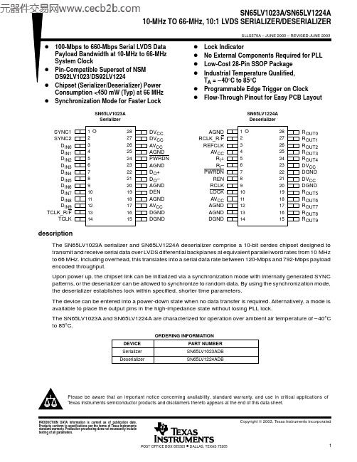
SYNC1 SYNC2 DIN0 DIN1 DIN2 DIN3 DIN4 DIN5 DIN6 DIN7 DIN8 DIN9 TCLK_R/F TCLK
1 2 3 4 5 6 7 8 9 10 11 12 13 14
28 27 26 25 24 23 22 21 20 19 18 17 16 15
Copyright 2003, Texas Instruments Incorporated
POST OFFICE BOX 655303
• DALLAS, TEXAS 75265
1
SN65LV1023A/SN65LV1224A 10-MHz TO 66-MHz, 10:1 LVDS SERIALIZER/DESERIALIZER
functional description (continued)
synchronization mode The deserializer PLL must synchronize to the serializer in order to receive valid data. Synchronization can be accomplished in one of two ways:
D Rapid Synchronization: The serializer has the capability to send specific SYNC patterns consisting of six
ones and six zeros switching at the input clock rate. The transmission of SYNC patterns enables the deserializer to lock to the serializer signal within a deterministic time frame. This transmission of SYNC patterns is selected via the SYNC1 and SYNC2 inputs on the serializer. Upon receiving valid SYNC1 or SYNC2 pulse (wider than 6 clock cycles), 1026 cycles of SYNC pattern are sent. When the deserializer detects edge transitions at the LVDS input, it attempts to lock to the embedded clock information. The deserializer LOCK output remains high while its PLL locks to the incoming data or SYNC patterns present on the serial input. When the deserializer locks to the LVDS data, the LOCK output goes low. When LOCK is low, the deserializer outputs represent incoming LVDS data. One approach is to tie the deserializer LOCK output directly to SYNC1 or SYNC2.
HLMP-BL11-N0T00中文资料

Agilent HLMP-ABxx, HLMP-BBxx, HLMP-ADxx, HLMP-BDxx, HLMP-AGxx, HLMP-BGxx, HLMP-ALxx, HLMP-BLxx,HLMP-AMxx, HLMP-BMxx T-13/4 (5 mm)Oval Precision Optical Performance AlInGaP and InGaN Lamps Data SheetFeatures•Well defined spatial radiation pattern•Viewing angles:Major axis 70°Minor axis 35°•High luminous output•Red and Amber Intensity are available for:AlInGaP (Bright)AlInGaP II (Brightest)•Colors:472 nm blue 526 nm green 626 nm red 630 nm red 590 nm amber 592 nm amber•Superior resistance to moisture •UV resistant epoxyBenefits•Viewing angle designed for wide field of view application•Red, green, and blue radiation patterns matched for full color sign•Superior performance in outdoor environments Applications•Full color/video signsDescriptionThese Precision O ptical Performance Oval LEDs are specifically designed for full color/video and passenger information signs. The oval shaped radiation pattern(35°x 70°) and high luminous intensity ensure that these devices are excellent for wide field of view outdoor application where a wide viewing angle and readability in sunlight areessential. These lamps have very smooth, matched radiation patterns ensuring consistent color mixing in full colorapplications, message uniformity across the viewing angle of the sign.High efficiency LED material is used in these lamps: Aluminum Indium Gallium Phosphide (AlInGaP) for amber and red,and Indium Gallium Nitride(InGaN) for blue and green. Each lamp is made with an advance optical grade epoxy offering superior high temperature and high moisture resistance in outdoor applications. The package epoxy contains both UV-A and UV-B inhibitors to reduce the effects of long term exposure to direct sunlight.Designers can select parallel or perpendicular orientation. Both lamps are available in tinted version.CAUTION: The blue and green LEDs are Class 1 ESD sensitive. Please observe appropriate precautions during handling and processing. Refer to Agilent Application Note AN-1142 for additio nal details.Table 1. Device Selection Guide for AlInGaP IIColor and Luminous Luminous ForwardDominant Intensity,Intensity,Voltage,LeadsWavelength I v (mcd) at I v (mcd) at V f (V)with Leadframe Package Part Numberλd (nm) Typ.20 mA Min.20 mA Max.Max.Stand-offs Orientation Drawing HLMP-AD06-P00xx Red 630880 2.4No Parallel A HLMP-AD06-P0Txx Red 630880 2.6No Parallel A HLMP-AD16-P00xx Red 630880 2.4Yes Parallel B HLMP-AD16-P0Txx Red 630880 2.6Yes Parallel B HLMP-AD16-RS0xx Red 63015002500 2.6Yes Parallel B HLMP-AD16-RSTxx Red 63015002500 2.6Yes Parallel B HLMP-AD16-RU0xx Red 63015004200 2.4Yes Parallel B HLMP-AD16-RUTxx Red 63015004200 2.6Yes Parallel B HLMP-AD16-ST0xx Red 63019003200 2.4Yes Parallel B HLMP-AD16-STTxx Red 63019003200 2.6Yes Parallel B HLMP-AL06-L00xx Amber 592400 2.4No Parallel A HLMP-AL06-L0Rxx Amber 592400 2.6No Parallel A HLMP-AL06-N00xx Amber 592680 2.4No Parallel A HLMP-AL06-N0Rxx Amber 592680 2.6No Parallel A HLMP-AL16-N00xx Amber 592680 2.4Yes Parallel B HLMP-AL16-N0Rxx Amber 592680 2.6Yes Parallel B HLMP-AL16-PSRxx Amber 5928802500 2.6Yes Parallel B HLMP-AL16-QR0xx Amber 59211501900 2.4Yes Parallel B HLMP-AL16-QRRxx Amber 59211501900 2.6Yes Parallel B HLMP-BD06-P00xx Red 630880 2.4No Perpendicular C HLMP-BD06-P0Txx Red 630880 2.6No Perpendicular C HLMP-BD06-RS0xx Red 63015002500 2.4No Perpendicular C HLMP-BD06-RSTxx Red 63015002500 2.6No Perpendicular C HLMP-BD16-P00xx Red 630880 2.4Yes Perpendicular D HLMP-BD16-P0Txx Red 630880 2.6Yes Perpendicular D HLMP-BD16-RU0xx Red 63015004200 2.4Yes Perpendicular D HLMP-BD16-RUTxx Red 63015004200 2.6Yes Perpendicular D HLMP-BD16-ST0xx Red 63019003200 2.4Yes Perpendicular D HLMP-BD16-STTxx Red 63019003200 2.6Yes Perpendicular D HLMP-BL06-N00xx Amber 592680 2.4No Perpendicular C HLMP-BL06-N0Rxx Amber 592680 2.6No Perpendicular C HLMP-BL06-QRKxx Amber 59211501900 2.4No Perpendicular C HLMP-BL06-QRSxx Amber 59211501900 2.6No Perpendicular C HLMP-BL16-N00xx Amber 592680 2.4Yes Perpendicular D HLMP-BL16-N0Rxx Amber 592680 2.6Yes Perpendicular D HLMP-BL16-PS0xx Amber 5928802500 2.4Yes Perpendicular D HLMP-BL16-PSRxx Amber 5928802500 2.6Yes Perpendicular DTable 2. LED IndicatorsDevice Selection Guide for AlInGaPColor and Luminous LuminousDominant Intensity,Intensity,LeadsWavelength I v (mcd) at I v (mcd) at with Leadframe Package Part Numberλd (nm) Typ.20 mA Min.20 mA Max.Stand-offs Orientation Drawing HLMP-AG01-K00xx Red 626310No Parallel A HLMP-AG11-KN0xx Red 626310880Yes Parallel B HLMP-AL01-K00xx Amber 590310No Parallel A HLMP-AL01-LP0xx Amber 5904001150No Parallel A HLMP-AL01-NR0xx Amber 5906801900No Parallel A HLMP-AL11-KN0xx Amber 590310880Yes Parallel B HLMP-AL11-NR0xx Amber 5906801900Yes Parallel B HLMP-BG01-LM0xx Red 626400520No Perpendicular C HLMP-BG01-MN0xx Red 626520880No Perpendicular C HLMP-BG11-KN0xx Red 626310880Yes Perpendicular D HLMP-BL01-NR0xx Amber 5906801900No Perpendicular C HLMP-BL11-KN0xx Amber 590310880Yes Perpendicular D HLMP-BL11-NR0xx Amber 5906801900Yes Perpendicular DTable 3. Device Selection Guide for InGaNColor and Dominant Luminous Intensity,Leads with Leadframe Package Part Number Wavelength λd (nm) Typ. Iv (mcd) at 20 mA Min.Stand-offs Orientation Drawing HLMP-AB01-J00xx Blue 472240No Parallel A HLMP-BB11-J00xx Blue 472240Yes Perpendicular D HLMP-BB11-K00xx Blue 472310Yes Perpendicular D HLMP-BM11-L00xx Green 526400Yes Perpendicular D HLMP-BM11-Q00xx Green 5261150Yes Perpendicular D HLMP-AB11-J00xx Blue 472240Yes Parallel B HLMP-AM01-Q00xx Green 5261150No Parallel A HLMP-BB01-J0Bxx Blue 472240No Perpendicular C HLMP-BB11-KN0xx Blue 472310Yes Perpendicular D HLMP-BM01-L00xx Green 526400No Perpendicular C Tolerance for intensity range limit is ±15%.Part Numbering SystemHLMP-X X X X - X X X XXMechanical Options00: Bulk PackagingDD: Ammo PackYY: Flexi-Bin; Bulk PackagingZZ: Flexi-Bin; Ammo PackColor Bin0: No Color Bin LimitationR: Color Bins 1, 2, 4, and 6 with V F max of 2.6 VT: Red Color with V F max of 2.6 VB: Color bin 2 and 3 onlyK: Color bins 2 and 4 onlyS: Color bins 2 and 4 with VF max of 2.6 VMaximum Intensity Bin0: No Iv Bin LimitationMinimum Intensity BinTint Option1 or 6: Matching Color TintsStandoff Option0: Without1: WithColorB: 472 nm BlueD: 630 nm RedG: 626 nm RedL: 590 or 592 nm AmberM: 526 nm GreenPackageA: 5 mm 35° x 70° Oval, ParallelB: 5 mm 35° x 70° O val, PerpendicularPackage Dimensions5.00 ±(0.197 ±8.71 ± 0.200.50 ± 0.10SQ. TYP.5.00 ±(0.197 ±5.00 ±(0.197 ±5.00 ±(0.197 ±ABCDNOTES:1. ALL DIMENSIONS ARE IN MILLIMETERS (INCHES).2. LEADS ARE MILD STEEL, SOLDER DIPPED.3. TAPERS SHOWN AT TOP OF LEADS (BOTTOM OF LAMP PACKAGE) INDICATE AN EPOXY MENISCUS THAT MAY EXTEND ABOUT 1 mm (0.040 IN.) DOWN THE LEADS.4. RECOMMENDED PC BOARD HOLE DIAMETERS:– LAMP PACKAGES A AND C WITHOUT STAND-OFFS: FLUSH MOUNTING AT BASE OF LAMP PACKAGE = 1.143/1.067 mm (0.044/0.042 IN.).– LAMP PACKAGES B AND D WITH STAND-OFFS: MOUNTING AT LEAD STAND-OFFS.Absolute Maximum Ratings at T A = 25˚CParameter Blue and Green Red and Amber DC Forward Current[1]30 mA50 mAPeak Pulsed Forward Current[2]100 mA100 mAAverage Forward Current30 mA30 mAReverse Voltage (I R = 100 µA) 5 VReverse Voltage (I R = 10 µA) 5 VPower Dissipation120 mW120 mWLED Junction Temperature130°C130°COperating Temperature Range–40°C to +80°C–40°C to +100°C Storage Temperature Range–40°C to +100°C–40°C to +120°C Wave Soldering Temperature[3]250°C for 3 seconds250°C for 3 seconds Notes:1.Derate linearly from Figure 7.2.Duty Factor 30% KHz.3.1.59 mm (0.060 in.) below body.Electrical/Optical Characteristics at T A = 25°CParameter Symbol Min.Typ.Max.Units Test Conditions Typical Viewing AngleMajor2θ1/270degMinor35Forward Voltage V F V I F = 20 mARed (λd = 626 nm) 2.0 2.4Red (λd = 630 nm)Option xx0xx 2.2 2.4Option xxTxx 2.3 2.6Amber (λd = 590 nm) 2.0 2.4Amber (λd = 592 nm)Option xx0xx 2.2 2.4Option xxRxx, xxSxx 2.3 2.6Blue (λd = 472 nm) 3.5 4.0Green (λd = 526 nm) 3.5 4.0Reverse VoltageAmber, Red V R520V I R = 100 µABlue, Green5–I R = 10 µAPeak Wavelength Peak of Wavelength of Amber (λd = 592 nm)λpeak594nm Spectral Distribution Red (λd = 630 nm)639at I F = 20 mABlue (λd = 472 nm)470Green (λd = 526 nm)524Spectral Halfwidth Wavelength Width Amber (λd = 592 nm)∆λ1/217nm at Spectral Distribution Red (λd = 630 nm)171/2 Power Point at Blue (λd = 472 nm)35I F = 20 mAGreen (λd = 526 nm)47Capacitance V F = 0, F = 1 MHz Amber, Red C40pFBlue, Green43Luminous Efficacy Emitted Luminous Amber (λd = 592 nm)ηv500lm/W Power/Emitted Radiant Red (λd = 630 nm)155Power at I F = 20 mA Blue (λd = 472 nm)75Green (λd = 526 nm)520Thermal Resistance RΘJ-PIN240°C/W LED Junction-to-Cathode LeadNotes:1.2θ1/2 is the off-axis angle where the luminous intensity is 1/2 the on-axis intensity.2.The radiant intensity, I e in watts per steradian, may be found from the equation I e = I v/ηv where I v is the luminous intensity in candelas and ηv isthe luminous efficacy in lumens/watt.3.The luminous intensity is measured on the mechanical axis of the lamp package.4.The optical axis is closely aligned with the package mechanical axis.5.The dominant wavelength, λd, is derived from theCIE Chromaticity Diagram and represents the color of the lamp.6.For Options -xxRxx, -xxSxx and -xxTxx, max. forward voltage (Vf) is 2.6 V. Refer to Vf bin table.Figure 1. Relative intensity vs. wavelength.Figure 2. Blue, green forward current vs.forward voltage.WAVELENGTH – nmR E L A T I V E I N T E N S I T Y1.00.500.40.30.20.10.60.70.80.9030251510I F – F O R W A R D C U R R E N T – m AV F – FORWARD VOLTAGE – V2.42.83.2 3.6520 2.6 3.0 3.4Figure 3a. Amber, red forward current vs.forward voltage.Figure 4. Blue, green relative luminous intensity vs. forward current.1.50.5I N T E N S I T Y N O R M A L I Z E D A T 20 m AI F – FORWARD CURRENT – mA01020301.051525C U R R E N T – m AV F – FORWARD VOLTAGE – V Figure 3b. Forward current vs. forward voltage for option -xxTxx red, and option -xxRxx and -xxSxx amber.D C F O R W A R D C U R RE N T – m AFORWARD VOLTAGE – VFigure 6. Blue, green maximum forward current vs. ambient temperature.Figure 7. Amber, red maximum forward current vs. ambient temperature.I F – F O R W A R D C U R R E N T – m A0T A – AMBIENT TEMPERATURE – °C40804020102060301005152535I F – F O R W A R D CU R R E N T – m AT A – AMBIENT TEMPERATURE – °CFigure 5. Amber, red relative luminous intensity vs. forward current.R E L A T I V E I N T E N S I T Y (N OR M A L I Z E D A T 20 m A )FORWARD CURRENT – mAFigure 8. Spatial radiation pattern – 35 x 70 degree lamps.R E L A T I V E I N T E N S I T Y – %1000VERTICAL ANGULAR DISPLACEMENT – DEGREES8060507020501030404020-10-30-50903010-20-40R E L A T I V E I N T E N S I T Y – %1000HORIZONTAL ANGULAR DISPLACEMENT – DEGREES8060507020501030404020-10-30-50903010-20-40Intensity Bin Limits (mcd at 20 mA)Bin Name Min.Max.G 140180H 180240J 240310K 310400L 400520M 520680N 680880P 8801150Q 11501500R 15001900S 19002500T 25003200U19002500Tolerance for each bin limit is ±15%.Amber Color Bin Limits (nm at 20 mA)Bin Name Min.Max.1584.5587.02587.0589.54589.5592.06592.0594.5Tolerance for each bin limit is ± 0.5 nm.Notes:1.All bin categories are established for classifi-cation of products. Products may not beavailable in all bin categories. Please contact your Agilent representative for further information.2. Vf bin table only available for those numbers with options -xxRxx, -xxSxx, -xxTxx.Blue Color Bin Limits (nm at 20 mA)Bin Name Min.Max.1460.0464.02464.0468.03468.0472.04472.0476.05476.0480.0Tolerance for each bin limit is ± 0.5 nm.Green Color Bin Limits (nm at 20 mA)Bin Name Min.Max.1520.0524.02524.0528.03528.0532.04532.0536.05536.0540.0Tolerance for each bin limit is ±0.5 nm.Vf Bin Table [2]Bin Id Min.Max.VA 2.0 2.2VB 2.2 2.4VC2.4 2.6/semiconductors For product information and a complete list of distributors, please go to our web site.For technical assistance call:Americas/Canada: +1 (800) 235-0312 or (916) 788-6763Europe: +49 (0) 6441 92460China: 10800 650 0017Hong Kong: (+65) 6756 2394India, Australia, New Zealand: (+65) 6755 1939 Japan: (+81 3) 3335-8152(Domestic/Interna-tional), or 0120-61-1280(Domestic Only) Korea: (+65) 6755 1989Singapore, Malaysia, Vietnam, Thailand, Philippines, Indonesia: (+65) 6755 2044 Taiwan: (+65) 6755 1843Data subject to change.Copyright © 2004 Agilent Technologies, Inc. August 27, 20045988-9224EN。
M12L64322A-5BG中文资料

57 NC 56 DQ31 55 VDDQ 54 DQ30 53 DQ29 52 VSSQ 51 DQ28 50 DQ27 49 VDDQ 48 DQ26 47 DQ25 46 VSSQ 45 DQ24 44 VSS
M12L64322A
512K x 32 Bit x 4 Banks Synchronous DRAM
ORDERING INFORMATION
86 Pin TSOP (TypeII) (400mil x 875mil)
Product No. MAX FREQ. PACKAGE COMMENTS
M12L64322A-5TG 200MHz TSOPII
Revision 1.9(Nov. 04 2005) - Modify tCC / tRCD spec
Revision 2.0(Dec. 08 2005) - Add –5T speed grade
Revision 2.1(Mar. 08 2006) - Modify Inch Dimension Max. A2 from 0.011 to 0.041
E VDDQ DQ31 NC
NC DQ16 VSSQ
F VSS DQM3 A3
A2 DQM2 VDD
G A4 A5 A6
A10 A0 A1
H A7 A8 NC
NC BA1 NC
J CLK CKE A9
BA0 CS RAS
K DQM1 NC NC
CAS WE DQM0
L VDDQ DQ8 VSS
VDD DQ7 VSSQ
Pb-free
12CWQ06FN中文资料

CT Typ. Junction Capacitance (Per Leg)
LS Typical Series Inductance (Per Leg)
(1) Pulse Width < 300µs,.61 0.79 0.57
0.72 3 35
0.36 24.14 360
(Per Leg)
10
10 0 10 20 30 40 50 60 70
Reverse V oltag e - V R (V ) Fig. 3 - Typical Junction Capacitance
Vs. Reverse Voltage (Per Leg)
Therm al Im pedance Z thJC ( C/W )
1000
T J= 25 C 100
Junction Capacitance - C T (pF)
1 0.2 0.4 0.6 0.8 1 1.2 1.4 1.6 1.8 2 2.2 2.4
Forward Voltage Drop - VFM (V) Fig. 1 - Max. Forward Voltage Drop Characteristics
320
Surge Current * See Fig. 7
105
EAS Non-Repet.Avalan.Energy(PerLeg)
7
IAR RepetitiveAvalancheCurrent
0.8
(Per Leg)
A 50% duty cycle @ TC = 131°C, rectangular wave form
VRRM
12
A
60
V
IFSM @ tp = 5 µs sine
EDI9LC644AV2012BC中文资料
N DQ12 DQ11
VCC
VSS
VSS
VSS
VCC DQ4 DQ0 N
P DQ13 DQ10
VCC
VSS SSCLK VSS
VCC DQ5 DQ1 P
R VCCQ VCCQ
VCC
VSS
VSS
VSS
VCC VCCQ VCCQ R
T DQ14 DQ9
VCC SSADC SSWE NC
VCC DQ6 DQ2 T
Input
DQ0-31 BWE0-3
Input Output
Input
Vcc, Vss VCCQ
Supply Supply
OUTPUT FUNCTIONAL DESCRIPTIONS
Signal Pulse Pulse Pulse Pulse Pulse Pulse
Level
Level Pulse
Polarity
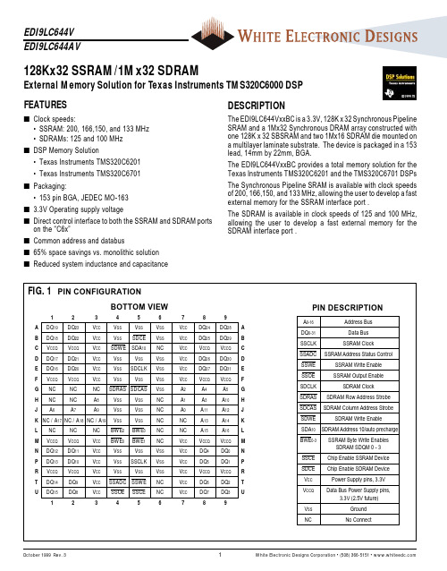
The EDI9LC644VxxBC provides a total memory solution for the Texas Instruments TMS320C6201 and the TMS320C6701 DSPs
The Synchronous Pipeline SRAM is available with clock speeds of 200, 166,150, and 133 MHz, allowing the user to develop a fast external memory for the SSRAM interface port .
2
DQ0-31
元器件交易网
EDI9LC644V EDI9LC644AV
Symbol
ALD1106中文资料

ADVANCED LINEAR DEVICES, INC.
ALD1106/ALD1116
QUAD/DUAL N-CHANNEL MATCHED MOSFET ARRAY
GENERAL DESCRIPTION
The ALD1106/ALD1116 are monolithic quad/dual N-channel enhancement mode matched MOSFET transistor arrays intended for a broad range of precision analog applications. The ALD1106/ALD1116 offer high input impedance and negative current temperature coefficient. The transistor pairs are matched for minimum offset voltage and differential thermal response, and they are designed for switching and amplifying applications in +2V to +12V systems where low input bias current, low input capacitance and fast switching speed are desired. These MOSFET devices feature very large (almost infinite) current gain in a low frequency, or near DC, operating environment. The ALD1106/ALD1116 are building blocks for differential amplifier input stages, transmission gates, and multiplexer applications, current sources and many precision analog circuits.
- 1、下载文档前请自行甄别文档内容的完整性,平台不提供额外的编辑、内容补充、找答案等附加服务。
- 2、"仅部分预览"的文档,不可在线预览部分如存在完整性等问题,可反馈申请退款(可完整预览的文档不适用该条件!)。
- 3、如文档侵犯您的权益,请联系客服反馈,我们会尽快为您处理(人工客服工作时间:9:00-18:30)。
0°
θ
180°
CONDUCTION ANGLE
AVERAGE FORWARD CURRENT VS. AMBIENT TEMPERATURE
W it h o u t F in o r P . C . B o a r d ,V R M = 6 0 V 11DQ06
1.6
D.C.
AVERAGE FORWARD CURRENT (A)
Approx Net Weight:0.32g 11DQ06 60 65 Ta=25°C* Ta=54°C* 50Hz Half Sine Wave Resistive Load Unit V V A A A °C °C Unit mA V °C/W
1.57 50Hz Half Sine Wave,1cycle, Non-repetitive - 40 to + 150 - 40 to + 150 Conditions Min. Typ. Max. 1 0.55 130 81
Maximum Ratings
Rating
Repetitive Peak Reverse Voltage Non-repetitive Peak Reverse Voltage Without Fin or Average Rectified P.C.Board Output Current P.C.Board mounted RMS Forward Current Surge Forward Current Operating JunctionTemperature Range Storage Temperature Range Symbol VRRM VRSM IO IF(RMS) IFSM Tjw Tstg Symbol IRM VFM 25 0.89 1.0
JUNCTION CAPACITANCE (pF)
100
50
20
10 0.5 1 2 5 10 20 50 100 REVERSE VOLTAGE (V)
P . C . B o a r d m o u n t e d (L = 8 m m ,P rin t L a n d 0 V 11DQ06
1.6
D.C.
AVERAGE FORWARD CURRENT (A)
1.2
RECT 180°. HALF SINE WAVE. RECT 120°.
AVERAGE REVERSE POWER DISSIPATION
11DQ06
AVERAGE REVERSE POWER DISSIPATION (W)
2.4
D.C.
2.0
RECT 300°
1.6
RECT 240°
1.2
RECT 180°
0.8
HALF SINE WAVE
0.4
0 0 10 20 30 40 50 60 70 REVERSE VOLTAGE (V)
Electrical • Thermal Characteristics
Characteristics
Peak Reverse Current Peak Forward Voltage Tj= 25°C, VRM= VRRM Tj= 25°C, IFM= 1.0A Without Fin or P.C.Board Thermal Resistance (Junction to Ambient) Rth(j-a) P.C.Board mounted *:Print Lands=5x5mm,Both Sides
0°
θ
180°
CONDUCTION ANGLE
AVERAGE FORWARD POWER DISSIPATION
11DQ06
D.C.
1.0
AVERAGE FORWARD POWER DISSIPATION (W)
0.8
RECT 180° HALF SINE WAVE RECT 120°
0.6
RECT 60°
20
15
10
5
0.02s
I FSM
0 0.02
0.05
0.1
0.2 TIME (s)
0.5
1
2
JUNCTION CAPACITANCE VS. REVERSE VOLTAGE
T j= 2 5 ° C ,V m = 2 0 m V R M S ,f = 1 0 0 k H z ,T yp ica l V a lu e 200 11DQ06
11DQ06 OUTLINE DRAWING (Dimensions in mm)
FORWARD CURRENT VS. VOLTAGE
11DQ06
5
INSTANTANEOUS FORWARD CURRENT (A)
2 Tj=25°C Tj=150°C 1
0.5
0.2
0.1 0 0.2 0.4 0.6 0.8 1.0 1.2 INSTANTANEOUS FORWARD VOLTAGE (V)
SBD
Type :11DQ06
OUTLINE DRAWING
FEATURES
* Miniature Size * Low Forward Voltage drop * Low Power Loss, High Efficiency * High Surge Capability * 30 Volts thru 100 Volts Types Available * 52mm Inside Tape Spacing Package Available
1.2
HALF SINE WAVE. RECT 120°.
0.8
RECT 60°.
RECT 180°.
0.4
0 0 25 50 75 100 125 150 AMBIENT TEMPERATURE (°C)
0°
θ
180°
CONDUCTION ANGLE
AVERAGE FORWARD CURRENT VS. AMBIENT TEMPERATURE
0.4
0.2
0 0 0.4 0.8 AVERAGE FORWARD CURRENT (A) 1.2 1.6
PEAK REVERSE CURRENT VS. PEAK REVERSE VOLTAGE
Tj= 150 °C 50 11DQ06
PEAK REVERSE CURRENT (mA)
20
10 0 10 20 30 40 50 60 70 PEAK REVERSE VOLTAGE (V)
0.8
RECT 60°.
0.4
0 0 25 50 75 100 125 150 AMBIENT TEMPERATURE (°C)
SURGE CURRENT RATINGS
f=50Hz,Half Sine Wave,Non-Repetitive,No Load 30 11DQ06
25
SURGE FORWARD CURRENT (A)