Precision electroweak constraints on Universal Extra Dimensions revisited
电子组件用元器件和零件的晶须试验方法-最新国标
电子组件用元器件和零件的晶须试验方法1范围本文件规定了对电气或电子元器件以及机械零件例如代表成品阶段的冲压/压印零件(例如,跳线、静电放电保护罩、机械固定件、压接针和电子元器件中使用的其他机械零件)的锡或锡合金表面处理的晶须试验的方法。
在要求的试验流程中,不考虑或评估模塑化合物、塑料等的物理尺寸变化。
试验方法是通过使用已知的方法开发的。
本文件也可用于二级供应商,如电镀车间、冲压车间或其他服务供应商,以确保供应链内表面质量的一致。
这些试验方法与相关部件或应用规范规定的验收标准一起使用。
本文件中描述的试验适用于初始鉴定,根据第7条进行定期监测,以及根据第9条对现有表面的工艺或制造工艺的改变。
本试验方法不包括连接器的接合区域。
SJ/T-10668-1995适用于连接器的接合区域。
2规范性引用文件下列文件中的内容通过文中的规范性引用而构成本文件必不可少的条款。
其中,注日期的引用文件,仅该日期对应的版本适用于本文件;不注日期的引用文件,其最新版本(包括所有的修改单)适用于本文件。
GB/T2421-2020环境试验概述和指南GB/T2423.22-2012环境试验第2部分:试验方法试验N:温度变化IEC60068-2-20环境试验-第2-20部分:试验-试验T:带引线器件的可焊性和耐焊接热的试验方法(Environmental testing-Part2-20:Tests-Test Ta and Tb:Test methods for solderability and resistance to soldering heat of devices with leads)IEC60068-2-58环境试验-第2-58部分:试验-试验Td:表面安装器件(SMD)的可焊性、耐金属溶解性和耐焊接热的试验方法(Environmental testing-Part2-58:Tests-Test Td:Test methods for solderability,resistance to dissolution of metallization and to soldering heat of surface mounting devices (SMD))IEC60068-2-67环境试验-第2-67部分:试验-试验Cy:主要用于部件的湿热、稳态、加速试验(Environmental testing-Part2-67:Tests-Test Cy:Damp heat,steady state,accelerated test primarily intended for components)IEC60068-2-78环境试验-第2-78部分:试验-试验室:湿热,稳态(Environmental testing-Part 2-78:Tests-Test Cab:Damp heat,steady state)IEC60512-16-21:2012电子设备连接器-试验和测量-第16-21部分:触点和终端的机械试验-试验16u:通过施加外部机械应力的晶须试验(Connectors for electronic equipment-Tests and measurements-Part16-21:Mechanical tests on contacts and terminations-Test16u:Whisker test via the application of external mechanical stresses)3术语和定义以下术语和定义适用于本文件。
半导体一些术语的中英文对照

半导体一些术语的中英文对照离子注入机ion implanterLSS理论Lindhand Scharff and Schiott theory 又称“林汉德-斯卡夫—斯高特理论"。
沟道效应channeling effect射程分布range distribution深度分布depth distribution投影射程projected range阻止距离stopping distance阻止本领stopping power标准阻止截面standard stopping cross section 退火annealing激活能activation energy等温退火isothermal annealing激光退火laser annealing应力感生缺陷stress—induced defect择优取向preferred orientation制版工艺mask—making technology图形畸变pattern distortion初缩first minification精缩final minification母版master mask铬版chromium plate干版dry plate乳胶版emulsion plate透明版see—through plate高分辨率版high resolution plate,HRP超微粒干版plate for ultra-microminiaturization 掩模mask掩模对准mask alignment对准精度alignment precision光刻胶photoresist又称“光致抗蚀剂"。
负性光刻胶negative photoresist正性光刻胶positive photoresist无机光刻胶inorganic resist多层光刻胶multilevel resist电子束光刻胶electron beam resistX射线光刻胶X-ray resist刷洗scrubbing甩胶spinning涂胶photoresist coating后烘postbaking光刻photolithographyX射线光刻X—ray lithography电子束光刻electron beam lithography离子束光刻ion beam lithography深紫外光刻deep—UV lithography光刻机mask aligner投影光刻机projection mask aligner曝光exposure接触式曝光法contact exposure method接近式曝光法proximity exposure method光学投影曝光法optical projection exposure method 电子束曝光系统electron beam exposure system分步重复系统step—and—repeat system显影development线宽linewidth去胶stripping of photoresist氧化去胶removing of photoresist by oxidation等离子[体]去胶removing of photoresist by plasma 刻蚀etching干法刻蚀dry etching反应离子刻蚀reactive ion etching,RIE各向同性刻蚀isotropic etching各向异性刻蚀anisotropic etching反应溅射刻蚀reactive sputter etching离子铣ion beam milling又称“离子磨削”。
Electron-Positron colliders
a r X i v :h e p -e x /0111070v 1 22 N o v 2001ELECTRON-POSITRON-COLLIDERSR.-D.HEUERInstitut f¨u r Experimentalphysik,Universit¨a t Hamburg,Luruper Chaussee 149,22761Hamburg GermanyE-mail:rolf-dieter.heuer@desy.deAn electron-positron linear collider in the energy range between 500and 1000GeV is of crucial importance to precisely test the Standard Model and to explore the physics beyond it.The physics program is complementary to that of the Large Hadron Collider.Some of the main physics goals and the expected accuracies of the anticipated measurements at such a linear collider are discussed.A short review of the different collider designs presently under study is given including possible upgrade paths to the multi-TeV region.Finally a framework is presented within which the realisation of such a project could be achieved as a global international project.1IntroductionA coherent picture of matter and forces has emerged in the past decades through in-tensive theoretical and experimental studies.It is adequately described by the Standard Model of particle physics.In the last few years many aspects of the model have been stringently tested,some to the per-mille level,with e +e −,ep and p ¯p machines making com-plementary contributions,especially to the determination of the electroweak bining the results with neutrino scatter-ing data and low energy measurements,the experimental analysis is in excellent concor-dance with the electroweak part of the Stan-dard Model.Also the predictions of QCD have been thoroughly tested,examples being precise measurements of the strong coupling αs and probing the proton structure to the shortest possible distances.Despite these great successes there are many gaps in our understanding.The clearest one is the present lack of any direct evidence for the dynamics of electroweak symmetry breaking and the generation of the masses of gauge bosons and fermions.The Higgs mechanism which generates the masses of the fundamental particles in the Standard Model,has not been experimentally estab-lished though the indirect evidence from pre-cision measurements is very strong.Even ifsuccessfully completed,the Standard Model does not provide a comprehensive theory of matter.There is no explanation for the wide range of masses of the fermions,the grand unification between the two gauge theories,electroweak and QCD,is not realised and gravity is not incorporated at the quantum level.Several alternative scenarios have been de-veloped for the physics which may emerge beyond the Standard Model as energies are increased.The Supersymmetric extension of the Standard Model provides a stable bridge from the presently explored energy scales up to the grand unification scale.Alternatively,new strong interactions give rise to strong forces between W bosons at high energies.Quite general arguments suggest that such new phenomena must appear below a scale of approximately 3TeV.Extra space dimen-sions which alter the high energy behaviour in such a way that the energy scale of gravity is in the same order as the electroweak scale are another proposed alternative.There are two ways of exploring the new scales,through attaining the highest possible energy in a hadron collider and through high precision measurements at the energy fron-tier of lepton colliders.This article is based on the results ofmany workshops on physics and detector studies for linear colliders.Much more can be found in the respective publications1,2,3,4 and on the different Web sites5,6,7,8.Many people have contributed to these studies and the references to their work can be found in the documents quoted above.2Complementarity of Lepton and Hadron MachinesIt is easier to accelerate protons to very high energies than leptons,but the detailed colli-sion process cannot be well controlled or se-lected.Electron-positron colliders offer a well√defined initial state.The collision energying generation of colliders.The physics case for such a machine will depend on the results from the LHC and the linear collider in the sub-TeV range.3Selected Physics TopicsIn this chapter,some of the main physics top-ics to be studied at a linear collider will bediscussed.Emphasis is given to the study of the Higgs mechanism in the Standard Model,the measurements of properties of su-persymmetric particles,and precision tests of the electroweak theory.More details about these topics as well as information about the numerous topics not presented here can be found in the physics books published in the studies of the physicspotential offuture lin-ear colliders 1,2,3,4.3.1Standard Model Higgs BosonThe main task of a linear electron-positron collider will be to establish experimentally the Higgs mechanism as the mechanism for generating the masses of fundamental parti-cles:•The Higgs boson must be discovered.•The couplings of the Higgs boson to gauge bosons and to fermions must be proven to increase with their masses.•The Higgs potential which generates the non-zero field in the vacuum must be reconstructed by determining the Higgs self-coupling.•The quantum numbers (J P C =0++)must be confirmed.The main production mechanisms for Higgs bosons in e +e −collisions are Higgs-strahlung e +e −→HZ and WW-fusion e +e −→νe ¯νe H ,and the corresponding cross-sections as a function of M H are depicted in figure 2for three different centre of mass en-ergies.With an integrated luminosity of 500Figure 2.The Higgs-strahlung and WW fusion pro-duction cross-sections as a function of M H for differ-ent√sof about 800GeV;for 1000fb −1an accuracyof 6%can be expected.The Higgs boson quantum numbers can be determined through the rise of the cross sec-tion close to the production threshold and through the angular distributions of the H and Z bosons in the continuum.Recoil Mass [GeV ]N u m b e r o f E v e n t s / 1.5 G e VFigure 3.The µ+µ−recoil mass distribution in theprocess e +e −→HZ →µ+µ−for M H =120GeV,500fb −1at√2of the self potential of the Higgs field V =λ(φ2−14λH4.The trilinearHiggs coupling λHHH =6λv can be mea-sured directly in the double Higgs-strahlung process e +e −→HHZ →q ¯q b ¯bb ¯b .The fi-nal state contains six partons resulting in a rather complicated experimental signature with six jets,a challenging task calling for ex-cellent granularity of the tracking device and the calorimeter 9.Despite the low cross sec-tion of the order of 0.2fb for M H =120GeV at√s =500GeV with an integrated luminosity of 1ab −1as shown in figure 6.Measurements of Higgs boson properties and their anticipated accuracies are sum-marised in table 1.In summary,the Higgs mechanism can be established in an unambiguous way at a high luminosity electron-positron collider with a centre-of-mass energy up to around one TeV as the mechanism responsible for the sponta-neous symmetry breaking of the electroweak interactions.3.2Supersymmetric ParticlesSupersymmetry (SUSY)is considered the most attractive extension of the Standardg c /g c (SM)g b /g b (S M )0.80.850.90.9511.051.11.151.2Figure 5.Higgs coupling determination:The con-tours for g b vs.g c for a 120GeV Higgs boson normalised to their Standard Model expectations as measured with 500fb −1.Model,which cannot be the ultimate the-ory for many reasons.The most impor-tant feature of SUSY is that it can explain the hierarchy between the electroweak scale of ≈100GeV,responsible for the W and Z masses,and the Planck scale M P l ≃1019GeV.When embedded in a grand-unified the-ory,it makes a very precise prediction of the electroweak mixing angle sin 2θW in excellent concordance with the precision electroweak measurement.In the following,only the min-imal supersymmetric extension to the Stan-dard Model (MSSM)will be considered and measurements of the properties of the super-symmetric particles will be discussed.Stud-ies of the supersymmetric Higgs sector can be found elsewhere 1,2,3,4.In addition to the particles of the Stan-dard Model,the MSSM contains their su-persymmetric partners:sleptons ˜l ±,˜νl (l =e,µ,τ),squarks ˜q ,and gauginos ˜g ,˜χ±,˜χ0.In the MSSM the multiplicative quantum num-ber R-parity is conserved,R p =+1for par-10012014016018000.20.10.3M H [GeV ]SM Double Higgs-strahlung: e + e - → ZHH σ [fb ]√s = 800 GeV√s = 500 GeVFigure 6.The cross-section for doubleHiggs-strahlung in the Standard Model at√120GeVmass 0.05%spin yes CPyes6%g HZZ 1%g HW W 2%g Hbb 2%g Hcc 10%g Hττ5%g Htt 6%λHHH∼30%ticles and R p =−1for sparticles.Spar-ticles are therefore produced in pairs and they eventually decay into the lightest spar-ticle which has to be stable.As an example,smuons are produced and decay through theprocess e +e −→˜µ+˜µ−→µ+µ−χ01χ01with χ01as the lightest sparticle being stable and,therefore,escaping detection.The mass scale of sparticles is only vaguely known.In most scenarios some spar-ticles,in particular charginos and neutrali-nos,are expected to lie in the energy region accessible by the next generation of e +e −200400600800Figure 7.Examples of mass spectra in mSUGRA,GMSB and AMSB models.colliders alsosupported bythe recentmea-surement of (g −2)µ10.Examples of massspectra for three SUSY breaking mechanisms (mSUGRA,GMSB,AMSB)are given in fig-ure 7.The most fundamental problem of super-symmetric theories is how SUSY is broken and in which way this breaking is communi-cated to the particles.Several scenarios have been proposed in which the mass spectra are generally quite different as illustrated in fig-ure 7.High precision measurements of the particle properties are therefore expected to distinguish between some of these scenarios.The study and exploration of Supersymmetry will proceed in the following steps:•Reconstruction of the kinematically ac-cessible spectrum of sparticles and the measurement of their properties,masses and quantum numbers•Extraction of the basic low-energy pa-rameters such as mass parameters,cou-plings,and mixings•Analysis of the breaking mechanism and reconstruction of the underlying theory.While it is unlikely that the complete spectrum of sparticles will be accessible at acollider with√Figure 9.Cross section near threshold for the processe +e −→˜χ+1˜χ−1,10fb−1per point.approach,the measured electroweak scaleSUSY parameters are extrapolated to high energies using these RGE’s.Due to the high precision of the measured input variables,only possible at the linear collider,an accurate test can be performed at which energy scale certain parameters be-come equal.Most interesting,the assump-tion of grand unification of forces requires the gaugino mass parameters M 1,M 2,M 3to meet at the GUT scale (figure 10(left)).Different SUSY breaking mechanisms predict different unification patterns of the sfermion mass parameters at high energy.With the high accuracy of the linear collider measure-ments these models can be distinguished as shown in figure 10for the case of mSUGRA (middle)and GMSB (right).In summary,the high precision studies of supersymmetric particles and their properties can open a window to energy scales far above the scales reachable with future accelerators,possibly towards the Planck scale where grav-ity becomes important.3.3Precision MeasurementsThe primary goal of precision measurements of gauge boson properties is to establish the non-abelian nature of electroweak interac-tions.The gauge symmetries of the Stan-dard Model determine the form and the strength of the self-interactions of the elec-troweak bosons,the triple couplings W W γand W W Z and the quartic couplings.Devi-ations from the Standard Model expectations for these couplings could be expected in sev-eral scenarios,for example in models where there exists no light Higgs boson and where the W and Z bosons are generated dynam-ically and interact strongly at high scales.Also for the extrapolation of couplings to high scales to test theories of grand unifi-cation such high precision measurements are mandatory.For the study of the couplings between gauge bosons the best precision is reached at the highest possible centre of mass energies.These couplings are especially sen-sitive to models of strong electroweak sym-metry breaking.W bosons are produced either in pairs,e +e −→W +W −or singly,e +e −→W eνwith both processes being sensitive to the triple gauge couplings.In general the total errors estimated on the anomalous couplings are in the range of few ×10−4.Figure 11com-pares the precision obtainable for ∆κγand ∆λγat different machines.The measurements at a linear collider are sensitive to strong symmetry breaking be-yond Λof the order of 5TeV,to be com-pared with the electroweak symmetry break-ing scale ΛEW SB =4πv ≈3TeV.One of the most sensitive quantities to loop corrections from the Higgs boson is the effective weak mixing angle in Z boson de-cays.By operating the collider at ener-gies close to the Z -pole with high luminos-ity (GigaZ)to collect at least 109Z bosons in particular the accuracy of the measure-Figure 10.Extrapolation of SUSY parameters measured at the electroweak scale to high energies.10-410-310-2∆κγLEP TEV LHCTESLA TESLA 50080010-410-310-2∆λγLEP TEV LHCTESLA TESLA500800Figure parison of constraints on the anomalous couplings ∆κγand ∆λγat different machinesment of sin 2θleff can be improved by one or-der of magnitude wrt.the precision obtained today 11.With both electron and positronbeams longitudinally polarised,sin 2θleff can be determined most accurately by measur-ing the left-right asymmetry A LR =A e =2v e a e /(v 2e +a 2e )with v e (a e )being the vec-tor (axialvector)couplings of the Z boson tothe electron and v e /a e =1-4sin 2θleff for pure Z exchange.Particularly demanding is the precision of 2×10⁻⁴with which the po-larisation needs to be known to match the statistical accuracy.An error in the weakmixing angle of ∆sin 2θleff =0.000013can be expected.Together with an improved de-termination of the mass of the W boson toa precision of some 6MeV through a scan of the W W production threshold and with the measurements obtained at high energy run-ning of the collider this will allow many high precision tests of the Standard Model at the loop level.As an example,figure 12shows the variation of the fit χ2to the electroweak measurements as a function of M H for the present data and for the data expected at a linear collider.The mass of the Higgs bo-son can indirectly be constraint at a level of 5%.Comparing this prediction with the di-rect measurement of M H consistency tests of the Standard Model can be performed at the quantum level or to measure free parameters in extensions of the Standard Model.This is5101520101032000LCm hχ2Figure 12.∆χ2as a function of the Higgs boson mass for the electroweak precision data today (2000)and after GigaZ running (LC).of particular importance if M H >200GeV in contradiction to the current electroweak mea-surements.In summary,there is strong evidence for new phenomena at the TeV energy scale.Only the precision exploration at the linear collider will allow,together with the results obtained at the Large Hadron Collider,the understanding of the underlying physics and will open a new window beyond the centre-of-mass energies reachable.Whatever sce-nario is realized in nature,the linear collider will add crucial information beyond the LHC.There is global consensus in the high energy physics community that the next accelera-tor based project needs to be an electron-positron linear collider with a centre-of-mass energy of at least 500GeV.4Electron-Positron Linear CollidersThe feasibility of a linear collider has been successfully demonstrated by the operationof the SLAC Linear Collider,SLC.How-ever,aiming at centre-of-mass energies at the TeV scale with luminosities of the order of 1034cm −2s −1requires at least two orders of magnitude higher beam power and two orders of magnitude smaller beam sizes at the inter-action point.Over the past decade,several groups worldwide have been pursuing differ-ent linear collider designs for the centre-of-mass energy range up to around one TeV as well as for the multi-TeV range.Excel-lent progress has been achieved at various test facilities worldwide in international col-laborations on crucial aspects of the collider designs.At the Accelerator Test Facility at KEK 12,emittances within a factor two of the damping ring design have been achieved.At the Final Focus Test Beam at SLAC 13de-magnification of the beams has been proven;the measured spot sizes are well in agreement with the theoretically expected values.The commissioning and operation of the TESLA Test Facility at DESY 14has demonstrated the feasibility of the TESLA technology.In the following,a short review of the different approaches is given.4.1TeV rangeThree design studies are presently pursued:JLC 15,NLC 16and TESLA 17,centred around KEK,SLAC and DESY,respectively.Details about the design,the status of de-velopment and the individual test facilities can be found in the above quoted references as well as in the status reports presented at LCWS200018,19,20.A comprehensive sum-mary of the present status can be found in the Snowmass Accelerator R&D Report 21,here only a short discussion of the main features and differences of the three approaches will be given with emphasis on luminosity and en-ergy reach.One key parameter for performing the physics program at a collider is the centre-of-mass energy achievable.The energy reachof a collider with a given linac length and a certain cavityfilling factor is determined by the gradient achievable with the cavity tech-nology chosen.For normalconducting cavi-ties the maximum achievable gradient scales roughly proportional to the RF frequency used,for superconducting Niobium cavities, the fundamental limit today is around55 MV/m.The second key parameter for the physicsprogram is the luminosity L,given byL=n b N2e f rep(σ∗x+σ∗y)2.Choos-ing aflat beam size(σ∗x≫σ∗y)at the inter-action point,δE becomes independent of the vertical beam size and the luminosity can be increased by reducingσ∗y as much as possi-ble.Sinceσ∗y∝sn b N e f rep=ηP AC is obtained from themains power P AC with an efficiency η.Equation(1)can then be rewritten asL∝ηP AC s ǫy(2)High luminosity therefore requires high ef-ficiencyηand high beam quality with low emittanceǫy and low emittance dilution ∆ǫ/ǫ∝f6RF,which is largely determined by the RF frequency f RF of the chosen technol-ogy.The fundamental difference between the three designs is the choice of technology for the accelerating structures.The design of NLC is based on normalconducting cavities using f RF of11.4GHz(X-band),for JLC two options,X-band or C-band(5.7GHz)are pursued.The TESLA concept,developed by the TESLA collaboration,is using supercon-ducting cavities(1.3GHz).As an example for a linear collider facility,figure13shows the schematic layout of TESLA.Figure13.Schematic layout of TESLATable2compares some key parameters for the different technologies at√Figure 14.Evolution of superconducting cavity per-formance.The average gradient achieved with TESLA 9-cell cavities produced in industry (first test,no additional processing)is shown as dots.with N b bunches,the time ∆T b between bunches within a train which allows head on crossing of the bunches for TESLA but requires a crossing angle for the other de-signs.The design luminosity L ,beam power P beam and the required mains power P AC il-lustrate that for a given mains power the su-perconducting technology delivers higher lu-minosity.On the other hand the lower gradi-ent G acc requires a longer linac for the samecentre-of-massenergy reach.As can be seen from table 2the X-band machines call for a beam loaded (unloaded)gradient of some 50(70)MV/m for√s =500GeV,a gradient which is mean-while routinely achieved for cavities fabri-cated in industry as illustrated in figure 14.Table 2also contains the presently planned length of the facilities 17,16,22,23.AnFigure 15.Excitation curves of three electropolished single-cell cavities.Gradients well above 35MV/m are reached.upgrade in energy up to around one TeV seems possible for all designs.In the NLC case,more cavities would be installed within the existing tunnel,in the JLC case,the tunnel length would have to be increased to house more cavities.In the TESLA case,a gradient of around 35MV/m is neededto reach√Table parison of some crucial parameters at 500GeV for the different technologies under study,see text for details.NLCJLC-C51502820190337 1.4head on angle 20.7σ∗x/y [nm ]245/2.7318/4.3δE [%]4.73.93.42.64P beam [MW ]13.212.6P AC (linacs )[MW ]13222023.550.23316s of 3TeV,usinghigh frequency (30GHz)normalcon-ducting structures operating at very high ac-celerating fields (150MV/m).The present design calls for bunch separations of .67ns,a vertical spotsize of 1nm and beamstrahlung δE of 30%.For this promising concept a new test facility is under construction at CERN which should allow tests with full gradient starting in 2005.5RealisationThe new generation of high energy colliders most likely exceeds the resources of a coun-try or even a region.There is general consen-sus that the realisation has to be done in an international,interregional framework.One such framework,the so called Global Accel-erator Network (GAN),has been proposed to ICFA in March 2000.A short discussion of the principle considerations will be presented here,more details can be found in ref.25.The GAN is a global collaboration of lab-oratories and institutes in order to design,construct,commission,operate and main-tain a large accelerator facility.The model is based on the experience of large experi-mental collaborations,particularly in particle physics.Some key elements are listed below:•it is not an international permanent in-stitution,but an international project of limited duration;•the facility would be the common prop-erty of the participating countries;•there are well defined roles and obliga-tions of all partners;•partners contribute through components or subsystems;•design,construction and testing of com-ponents is done in participating institu-tions;•maintenance and running of the accel-erator would be done to a large extent from the participating institutions.The GAN would make best use of world-wide competence,ideas and resources,create a visible presence of activities in all partici-pating countries and would,hopefully,make the site selection less controversial.study general considerations of implementing a GAN and to study the technical considera-tions and influence on the design and cost of the accelerator.The reports of these working groups can be found on the web26.Their overall conclusion is that a GAN can be a fea-sible way to build and operate a new global accelerator,although many details still need to be clarified.6SummaryThere is global consensus about the next ac-celerator based project in particle physics.It has to be an electron-positron linear collider with an initial energy reach of some500GeV with the potential of an upgrade in centre-of-mass energy.The physics case is excellent, only a few highlights could be presented here. There is also global consensus that concur-rent operation with LHC is needed and fruit-ful.Therefore,a timely realisation is manda-tory.The technical realisation of a linear col-lider is now feasible,several technologies are either ripe or will be ripe soon.A fast consen-sus in the community about the technology is as a global project with the highest possible luminosity and a clear upgrade potential be-yond500GeV.AcknowledgmentsThe author would like to express his grati-tude to all people who have contributed to the studies of future electron-positron linear colliders from the machine design to physics and detector studies.Special thanks go to the organisers and their team for a very well or-ganised,inspiring conference as well as for the competent technical help in preparing this presentation.References1.J.A.Aguilar-Saavedra et al,TESLATechnical Design Report,Part III,Physics at an e+e−Linear Collider,DESY2001-011,ECFA2001-209,hep-ph/0106315.2.T.Abe et al,Linear Collider Physics Re-source Book for Snowmass2001,BNL-52627,CLNS01/1729,FERMILAB-Pub-01/058-E,LBNL-47813,SLAC-R-570,UCRL-ID-143810-DR,LC-REV-2001-074-US,hep-ex/0106055-583.K.Abe et al,Particle Physics Exper-iments at JLC,KEK-Report2001-11, hep-ph/0109166.4.Proceedings of LCWS,Physics and Ex-periments with Future Linear Colliders, eds A.Para,H.E.Fisk,(AIP Conf.Proc.,Vol578,2001).5.Worldwide Study of the Physics and De-tectors for Future e+e−Colliders/lc/6.ACFA Joint Linear Collider Physics andDetector Working Grouphttp://acfahep.kek.jp/7.2nd Joint ECFA/DESY Studyon Physics and Detectors for a Linear Electron-Positron Colliderhttp://www.desy.de/conferences/ecfa-desy-lc98.html8.A Study of the Physics and Detectors forFuture Linear e+e−Colliders:American Activities/lc/ameri-ca.html9.G.Alexander et al,TESLA TechnicalDesign Report,Part IV,A Detector for TESLA,DESY2001-011,ECFA2001-209.10.H.N.Brown et al.[Muon g-2Collabo-ration],Phys.Rev.Lett.86(2001)222711.J.Drees,these proceedings12.E.Hinode et al,eds.,KEK Internal95-4,1995,eds J.Urakawa and M.Yoshioka, Proceedings of the SLAC/KEK Linear Collider Workshop on Damping Ring, KEK92-6,199213.The FFTB Collaboration:BINP(Novosibirsk/Protvino),DESY, FNAL,KEK,LAL(Orsay),MPI Mu-nich,Rochester,and SLAC14.Proposal for a TESLA Test Facility,DESY TESLA-93-01,199215.KEK-Report97-1,1997.16.Zeroth Order Design Report for theNext Linear Collider,SLAC Report474,1996.2001Report on the Next Linear Collider,Fermilab-Conf-01-075-E,LBNL-47935,SLAC-R-571,UCRL-ID-14407717.J.Andruszkow et al,TESLA TechnicalDesign Report,Part II,The Accelerator, DESY2001-011,ECFA2001-20918.O.Napoly,TESLA Linear Collider:Sta-tus Report,in ref419.T.O.Raubenheimer,Progress in theNext Linear Collider Design,in ref4 20.Y.H.Chin et al Status of JLC Accelera-tor Development,in ref421.A.Chao et al,2001Snowmass Accelera-tor R&D Report,http://www.hep.anl.gov/pvs/dpb/Snowmass.pdf22.Y.H.Chin,private communication23.H.Matsumoto,T.Shintake,private com-munication24.I.Wilson,A Multi-TeV Compact e+e−Linear Collider,in ref425.F.Richard et al,TESLA Technical De-sign Report,Part I,Executive Summary, DESY2001-011,ECFA2001-209,hep-ph/0106314.26./directorate/icfa/icfa reports.html。
电桥测试仪专业英文词汇

电桥测试仪专业英文词汇电桥测试仪的专业英文术语是"bridge tester" 或"bridge measurement instrument"。
这些术语常用于描述用于电学测量和测试电阻、电容或电感等参数的设备。
以下是与电桥测试仪相关的专业英文词汇:1.Bridge Circuit - 桥式电路2.Resistance Measurement - 电阻测量3.Impedance Measurement - 阻抗测量4.Balancing the Bridge - 调平电桥5.Wheatstone Bridge - 惠斯通电桥6.Galvanometer - 电流计7.Inductance - 电感8.Capacitance - 电容9.Accuracy - 精度10.Calibration - 校准11.Measurement Range - 测量范围12.Test Voltage - 测试电压13.Four-Point Probe - 四探针测量14.Kelvin Bridge - 开尔文电桥15.Test Leads - 测试引线16.Ohmmeter - 电阻表17.Multimeter - 多用途表18.Thermal Compensation - 温度补偿19.Null Detector - 零差检测器20.Measuring Circuitry - 测量电路21.Guarding - 防护22.Uncertainty Analysis - 不确定度分析23.Test Signal Generator - 测试信号发生器24.Bridge Balance Indicator - 电桥平衡指示器25.Measurement Error - 测量误差这些词汇有助于描述电桥测试仪的原理、功能和操作。
电子设备结构件术语中英对照
电子设备结构件术语中英对照电子设备是现代工业中不可缺少的一部分,电子设备结构件是构成电子设备的重要组成部分,而其中的术语也是非常重要的技术术语。
在现代国际化的环境下,学习这些术语的中英对照是非常必要的。
本文将会给大家介绍一些常见的电子设备结构件术语的中英对照,旨在帮助大家更好地学习电子设备相关知识。
1. 电阻器(Resistor)电阻器是电子设备结构件中最常见的一种,主要用于电路中调整电流、电压、功率等参数。
在电路中,电阻器有时也被称为电阻或阻值。
电阻器有许多不同的类型,包括固定电阻器、变阻器、可变电阻器等。
如:- 固定电阻器(Fixed Resistor)- 变阻器(Potentiometer 或Variable Resistor)- 可变电阻器(Trim Pot 或Trimming Potentiometer)2. 电容器(Capacitor)电容器也是电子设备结构件中常见的一种,主要用于调整电路的电容量以及滤波、耦合等功能。
电容器的主要特点是两个电极之间带有介质,同时若电容器通过交流电,就会在介质周围产生电磁场。
电容器也有许多不同类型,包括电解电容器、陶瓷电容器、金属膜电容器等。
如:- 电解电容器(Electrolytic Capacitor)- 陶瓷电容器(Ceramic Capacitor)- 金属膜电容器(Metal Film Capacitor)3. 电感器(Inductor)电感器是一个由电流所产生磁场所组成的电路结构件。
它主要用于保持电流、电压等值的稳定性。
电感器通常由铁芯和线圈组成,其中线圈上的导线被绕在铁芯上,当电流通过线圈时,即可产生磁场。
电感器有许多不同类型,包括空心线圈电感器、铁芯线圈电感器等。
如:- 空心线圈电感器(Air Core Inductor)- 铁芯线圈电感器(Iron Core Inductor)4. 二极管(Diode)二极管是一种由半导体材料制成的电子设备结构件,它是一个只允许电流在一个方向(正向)通过的电路元件,而在相反方向(反向)则会阻塞电流传导。
Weak Interactions of Light Flavours
LSM = LH (φ) + LG (W, Z, G) + Higgs Gauge ¯ / ψ+ ψiD
ψ=fermions ψ,ψ′ =fermions
The Standard Model Lagrangian has four parts: ¯ ′ gψψ′ ψφψ Yukawa
QCD and QED conserve C,P,T separately. Local Field theory by itself implies CPT. The fermion and Higgs2 part of the SM-lagrangian conserves CP and T as well. The only part that violates CP and as a consequence also T is the Yukawa part. The Higgs part is responsible for two parameters, the gauge part for three and the HiggsFermion part contains in principle 27 complex parameters, neglecting Yukawa couplings to neutrinos. Luckily most of the 54 real parameters in the Yukawa sector are unobservable. After diagonalizing the lepton sector there only the three charged lepton masses remain. The quark sector can be similarly diagonalized leading to 6 quark masses, but some parts remain in the difference between weak interaction eigenstates and mass-eigenstates. The latter is conventionally put in the couplings of the charged W -boson, which is given by Vud Vus Vub dα g α − uα cα t γ µ (1 − γ5 ) Vcd Vcs Vcb sα − √ Wµ 2 2 V V V b
半导体激光器制造工艺英文

半导体激光器制造工艺英文英文回答:Semiconductor Laser Manufacturing Process.The manufacturing process of semiconductor lasers involves several key steps, including:1. Epitaxial Growth: A thin layer of semiconductor material is grown on a substrate using a process called molecular beam epitaxy (MBE) or metal-organic chemical vapor deposition (MOCVD). This layer forms the active region of the laser.2. Mesa Etching: The active region is patterned using photolithography and etching techniques to create a mesa structure. The mesa defines the lateral dimensions of the laser cavity.3. Cleaving: The wafer is cleaved along specificcrystallographic planes to create the laser facets. The facets provide optical feedback for the laser cavity.4. Metallization: Ohmic contacts are deposited on the facets and the top of the mesa to provide electrical connections.5. Packaging: The laser chip is mounted on a heat sink and packaged to provide protection and thermal management.Various additional steps may be employed to enhance laser performance, such as:Anti-reflective (AR) Coating: AR coatings are applied to the facets to minimize optical losses.High-reflective (HR) Coating: HR coatings are used to improve cavity feedback and increase laser output power.Facet Passivation: Facet passivation techniques are used to prevent degradation and improve laser reliability.中文回答:半导体激光器制造工艺。
微电子专业英语词汇
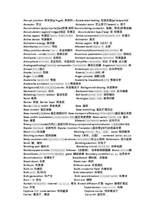
Abrupt junction 突变结[ə'brʌpt] 突然的;Accelerated testing 加速实验[ək'seləreitid] Acceptor 受主Acceptor atom 受主原子['ætəm] n. 原子Accumulation [ə,kju:mju'leiʃən]积累,堆积Accumulating contact(n. 接触,联系)积累接触Accumulation region['ri:dʒən]地区积累区Accumulation layer['leiə] 层积累层Active region 有源区['æktiv]积极的,有源的Active component [kəm'pəunənt]元件有源元Active device 有源器件Activation 激活Activation energy 激活能Active region 有源(放大)区Admittance [əd'mitəns]导纳Allowed band [bænd]带允带Alloy-junction device ['ælɒɪ]合金结器件Aluminum(Aluminium) [ə'lju:minəm]铝Aluminum – oxide ['ɔksaid]铝氧化物Aluminum passivation [pæsi'veiʃən]钝化铝钝化Ambipolar [,æmbi'pəulə]双极的Ambient temperature ['æmbiənt]环境温度Amorphous [ə'mɔ:fəs]无定形的,非晶体的Amplifier ['æmplifaiə]功放扩音器放大器Analogue(Analog) ['ænəlɔɡ] comparator ['kəmpəreitə]模拟比较器Angstrom['æŋstrəm]埃Anneal [ə'ni:l]退火Anisotropic [æn,aisəu'trɔpik]各向异性的Anode ['ænəud]阳极Arsenic ['ɑ:sənik (AS) 砷Auger ['ɔ:ɡə]俄歇Auger process 俄歇过程Avalanche ['ævəlɑ:ntʃ]雪崩Avalanche breakdown(击穿) 雪崩击穿Avalanche excitation [,eksi'teiʃən](激发)雪崩激发Background(背景,本底,基底) carrier 本底载流子Background doping 本底掺杂Backward ['bækwəd]反向Backward bias ['baiəs](偏置,)偏爱反向偏置Ballasting ['bæləst] resistor 整流电阻Ball bond [bɔnd](结合)球形键合Band 能带Band gap [ɡæp](间隙)能带间隙Barrier 势垒Barrier layer 势垒层Barrier ['bæriə] width 势垒宽度Base 基极Base contact 基区接触Base stretching 基区扩展效应Base transit(运输)time基区渡越时间Base transport efficiency [i'fiʃənsi](效率)基区输运系数Base-width modulation [,mɔdju'leiʃən(调制)基区宽度调制Basis vector ['vektə]矢量基矢Bias 偏置Bilateral [,bai'lætərəl] switch 双向开关Binary ['bainəri]code(代码)二进制代码Binary compound semiconductor二元化合物半导体Bipolar [bai'pəulə]双极性的Bipolar Junction Transistor (晶体管)(BJT)双极晶体管Bloch [blɔk]布洛赫Blocking ['blɔkiŋ](截止,阻塞)band 阻挡能带Blocking contact 阻挡接触Body(身体,主题)- centered(居中的)体心立方Body-centred cubic ['kju:bik]立方体structure ['strʌktʃə]结构体立心结构Boltzmann 波尔兹曼Bond 键、键合Bonding electron 价电子Bonding pad 键合点Bootstrap circuit ['sə:kit]电路自举电路Bootstrapped emitter [i'mitə]发射器follower(追随者)自举射极跟随器Boron ['bɔ:rɔn]硼Borosilicate [,bɔ:rəu'silikit]硼硅酸盐glass 硼硅玻璃Boundary condition条件,状况边界条件Bound electron 束缚电子Breadboard 模拟板、实验板Break down 击穿Break over 转折Brillouin 布里渊Brillouin zone 布里渊区Built-in 内建的Build-in electric field 内建电场Bulk [bʌlk]体/体内Bulk absorption 体吸收Bulk generation 体产生Bulk recombination [,ri:kɔmbi'neiʃən]体复合Burn - in 老化Burn out 烧毁Buried ['berid]埋葬的channel通道;频道;海峡埋沟Buried diffusion扩散region 隐埋扩散区Can 外壳Capacitance[kə'pæsɪt(ə)ns]电容Capture俘获cross section 俘获截面Capture carrier 俘获载流子Carrier 载流子、载波Carry bit 进位位Carry-in bit 进位输入Carry-out bit 进位输出Cascade [kæs'keid]级联,串联级联Case 管壳Cathode['kæθəud]阴极Center 中心Ceramic [si'ræmik]陶瓷(的)Channel['tʃænəl] (频道)沟道Channel breakdown 沟道击穿Channel current 沟道电流Channel doping 沟道掺杂Channel shortening 沟道缩短Channel width 沟道宽度Characteristic impedance[im'pi:dəns]特征阻抗Charge (控告)电荷,充电Charge-compensation[,kɔmpen'seiʃən](补偿) effects 电荷补偿效应Charge conservation(保存,保持) 电荷守恒Charge neutrality[njuː'trælɪtɪ](中性) condition电中性条件Charge drive/exchange/sharing/transfer/storage 电荷驱动/交换/共享/转移/存储Chemmical etching[njuː'trælɪtɪ]化学腐蚀法Chemically-Polish['pɒlɪʃ](磨光)化学抛光Chemmically-Mechanically [mɪ'kænɪkəlɪ](机械地)Polish (CMP) 化学机械抛光Chip 芯片Chip yield(产量)芯片成品率Clamped 箝位Clamping diode 箝位二极管Cleavage['kliːvɪdʒ] plane(平面)解理面Clock rate(比率)时钟频率Clock generator 时钟发生器Clock flip-flop(触发器)时钟触发器Close-packed structure(构造)密堆积结构Close-loop(环)gain(获利,增加)闭环增益Collector 集电极Collision[kə'lɪʒ(ə)n](冲突)碰撞Compensated(补偿)OP-AMP 补偿运放Common-base/collector/emitter connection 共基极/集电极/发射极连接Common-gate/drain/source connection 共栅/漏/源连接Common-mode gain 共模增益Common-mode input 共模输入Common-mode rejection(抑制,拒绝)ratio (CMRR) 共模抑制比Compatibility[kəm,pætɪ'bɪlɪtɪ]兼容性Compensation 补偿Compensated impurities(杂质)补偿杂质Compensated semiconductor 补偿半导体Complementary(补足的)Darlington circuit(电路,回路)互补达林顿电路Complementary Metal-Oxide-Semiconductor Field-Effect-Transistor(晶体管)(CMOS) 互补金属氧化物半导体场效应晶体管Complementary error function(功能,函数)余误差函数Computer-aided【辅助的】design (CAD)/test(CAT)/manufacture(CAM) 计算机辅助设计/ 测试/制造Compound['kɒmpaʊnd] Semiconductor 化合物半导体Conductance[kən'dʌkt(ə)ns]电导Conduction(传导band (edge) 导带(底) Conduction level/state 导带态Conductor 导体Conductivity 电导率Configuration(配置)组态Conlomb['kuːlɒm]库仑Conpled Configuration Devices 结构组态Constants(常量,常数)物理常数Constant energy surface 等能面Constant-source diffusion(扩散,传播)恒定源扩散Contact(联系,接触)接触Contamination[kən,tæmɪ'neɪʃən]玷污Continuity[,kɒntɪ'njuːɪtɪ](连续性)equation(方程式,等式)连续性方程Contact hole孔接触孔Contact potential(潜能,潜在的)接触电势Continuity condition 连续性条件Contra['kɒntrə]相反doping 反掺杂Controlled 受控的Converter[kən'vɜːtə](converter转变,转换)转换器Conveyer[kən'veɚ]传输器Copper(铜)interconnection[,ɪntɚkə'nɛkʃən](互联)system 铜互连系统Couping 耦合Covalent[kəʊ'veɪl(ə)nt](共价的)共阶的Crossover 跨交Critical (批评的)临界的Crossunder 穿交Crucible['kruːsɪb(ə)l]坩埚Crystal defect缺陷/face/orientation/lattice 晶体缺陷/晶面/晶向/晶格Current density(密度)电流密度Curvature'kɜːvətʃə曲率Cut off 截止Current drift(漂移)/dirve/sharing电流漂移/驱动/共享Current Sense(感觉,检测)电流取样Curvature 弯曲Custom(风俗,习惯,定制的integrated circuit 定制集成电路Cylindrical 柱面的Czochralshicrystal 直立单晶crystal(晶体,单晶)Czochralski technique 切克劳斯基技术(Cz 法直拉晶体J)Dangling ['dæŋg(ə)lɪŋ;bonds 悬挂键Dark current 暗电流Dead time 空载时间Debye length 德拜长度De.broglie 德布洛意Decderate 减速Decibel ['desɪbel] (dB) 分贝Decode 译码Deep acceptor level 深受主能级Deep donor['dəʊnə(捐赠者level 深施主能级Deep impurity(杂质,不存,不洁)level 深度杂质能级Deep trap 深陷阱Defeat 缺陷Degenerate semiconductor 简并半导体Degeneracy 简并度Degradation[,degrə'deɪʃ(ə)n]退化Degree Celsius(centigrade) /Kelvin 摄氏/开氏温度Delay 延迟Density 密度Density of states 态密度Depletion 耗尽Depletion approximation 耗尽近似Depletion contact 耗尽接触Depletion depth 耗尽深度Depletion effect 耗尽效应Depletion layer 耗尽层Depletion MOS 耗尽MOSDepletion region 耗尽区Deposited film(电影,薄膜) 淀积薄膜Deposition process 淀积工艺Design rules 设计规则Die 芯片(复数dice)Diode 二极管Dielectric 介电的Dielectric isolation(隔离。
三维半导体存储器件[发明专利]
![三维半导体存储器件[发明专利]](https://img.taocdn.com/s3/m/dec80c807e21af45b207a872.png)
专利名称:三维半导体存储器件专利类型:发明专利
发明人:李奉镕,金泰勋,裵敏敬申请号:CN201910639467.3申请日:20190716
公开号:CN110729304A
公开日:
20200124
专利内容由知识产权出版社提供
摘要:一种三维(3D)半导体存储器件可以包括:堆叠结构,包括顺序地堆叠在衬底上的栅电极;以及穿透堆叠结构的垂直沟道。
栅电极可以包括顺序地堆叠在衬底上的地选择栅电极、单元栅电极、串选择栅电极和擦除栅电极。
申请人:三星电子株式会社
地址:韩国京畿道
国籍:KR
代理机构:北京市柳沈律师事务所
代理人:张波
更多信息请下载全文后查看。
华新电阻规格书
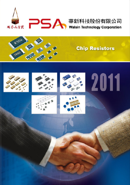
Functional code X : Thick film low ohm M : Metal low ohm N : Metal low ohm, high power W : Thick film low TCR P : Thick film low TCR high power ( 2512 size=2 watt, 2010 size=1 watt, 1210 size=0.5 watt, 1206 size=0.5 watt,
R002
Tolerance F : +/- 1% J : +/- 5% P : Jumper
Packaging code P : 4” reel taping T : 7” reel taping A : 7” reel taping 15Kpcs Q : 10” reel taping G : 13” reel taping R : 0603 2mm pitch taping B : Bulk K : Bulkcase
Termination code L = Sn base (Lead free) 5 3E SSP (total)
WW
25
M
F
T
L
Type code WW: R< 1ohm MW: R< 1ohm Automotive SW: R< 1ohm Anti-sulfuration
Size code 25 : 2512 (6432) 20 : 2010 (5025) 18 : 1218 (3248) 12 : 1206 (3216) 10 : 1210 (3225) 08 : 0805 (2012) 06 : 0603 (1608) 04 : 0402 (1005)
彭博工艺发电机Series 5000 0.2毫米精确设置全金属刀刃 60分钟无线电使用 每小时充电

Beardtrimmer series 50000.2mm precision settingsFull metal blades60 min cordless use/1h charge Integrated hair lift combBT5200/15Effortless even trimDynamic beard guide system for an even result This trimmer with full metal blades lets you achieve exactly the 3-day stubble, short beard, or long beard look you want. Our new integrated hair lift comb raises hairs for efficient one pass even trimming resultsEffortless trimmingLifts the hair up to the level of the blade for even resultsGuides the hairs to the cutter for effortless trimmingBlades are double sharpened for faster trimming*Skin-friendly performanceSkin-friendly, high-performance blades for the perfect trimPerfect 3 day stubbleKeep perfect 3-day stubble by using the 0.4mm setting dailyEasy to use17 Lock-in length settings, 0,4 - 10mm with 0,2mm precision60 minutes runtime after a 1 hour charge, or plug it in100% waterproof for easy, thorough cleaning2 year guarantee, worldwide voltage and no need to oilHighlightsDynamic Beard Guide SystemThe Dynamic Beard Guide system with the help of the integrated hair lift comb lifts the hairs up to the level of the blades for even trimming results and lets you achieve exactly the 3-day stubble, short beard, or long beard look you want.Integrated Hair lift combTrim your stubble in one quick pass, while being gentle on your skin. Our new Integrated hair lift comb lifts and guides the hairs to the level of the blades for effortless, even trimming.Full metal bladesThis trimmer comes with double sharpened full metal blades that cuts more hairs in every pass for faster trimming.17 lock-in length settingsSelect your preferred trim length by simplyturning the zoom wheel on the handle until the length you want is displayed from 0,4 - 10mm with 0,2mm precision. Your chosen length is now "locked in" for a perfectly even trim.Corded and cordless useCharge your beard trimmer for 1 hour to get 60minutes of cordless use. If you need more energy while trimming, you can simply plug the trimmer into the wall. This trimmer has been designed to run both cordless and plugged in.100% waterproofSimply rinse your waterproof beard trimmer under the tap to thoroughly clean it.Skin-friendly bladesGet a perfect yet protective trim, time after time.The beard trimmer's steel blades lightly brush against one another, sharpening themselves as they trim so they stay extra sharp and effective.They also have rounded tips and combs tohelp prevent skin irritation.iF DESIGN AWARD 2016Beardtrimmer series 5000iF DESIGN AWARD2016Philips Green LogoPhilips Green Products can reduce costs,energy consumption and CO2 emissions. How?They offer a significant environmentalimprovement in one or more of the Philips Green Focal Areas – Energy efficiency,Packaging, Hazardous substances, Weight,Recycling and disposal and Lifetime reliability.Red Dot Award 2016: WinnerBeard trimmer series 5000Red Dot Award 2016: WinnerSpecificationsCutting systemPrecision (size of steps): From 0.2mm Cutting element: Stainless steel blades Non-scratching teeth: For more comfort Create the look you wantNumber of length settings: 17 integrated length settingsAccessoriesComb: Integrated hair lift comb Maintenance: Cleaning brush Ease of useCleaning: Fully washableZoom wheel: Easily adjust length settingsDisplay: Battery lightOperation: Corded & Cordless useDesignColor: BlackPowerRun time: 60 minutesCharging: 1 hour full chargeAutomatic voltage: 100-240 VService2-year guaranteeNo oil needed* Versus its Philips predecessor© 2019 Koninklijke Philips N.V.All Rights reserved.Specifications are subject to change without notice. Trademarks are the property of Koninklijke Philips N.V. or their respective owners.Issue date 2019‑07‑02 Version: 5.3.1EAN: 08 71010 37186 11 。
精密电路公司 160 225A 电池隔离管理器说明书

Precision Circuits Inc2538 Wisconsin Ave, Downers Grove, IL 60515 630-515-9100Battery Isolation ManagerRev 7Key Features:1. 160amp & 225amp continuous models available2. Runs cooler using less powera. Draws no current in ON or OFF stateb. Excellent for Solar Panel use3. Microprocessor baseda. Monitors battery state over longer periods of timeb. Not simply voltage dependent4. a. Approved for Battery Compartments b. Ignition Proof, SAE J1171 c. Waterproof, I EC 60529, IP66 IP67, A STM B 117 96 Hours Salt Spray5. Chargesa. Coach Battery from Alternatorb. Chassis Battery from Coach Charger6. Isolates Batteries to prevent discharging or overcharging of Batteries7. Preventsa. Equalization cycles from Damaging Chassis Batteryb. Annoying clicking of Isolator Relayc. Overcharging of Coach Battery during long drivesd. Overcharging of Chassis Battery during long stays8. Provides Emergency Start with Dash Switch. O ptional power connection for existing applications, and ground connection to allow Emergency Start of either battery.9. Weighs under 1 poundThe Battery Isolation Manager (BIM) isolates the two battery systems, chassis, and coach, in a motorhome. This prevents loads in one system from discharging both. It also connects the two battery systems together during charging. Both batteries are charged if either is being charged. The coachbattery is charged while driving and the chassis battery is charged while plugged into Shore Power at a campground. The BIM monitors the battery voltage of both the chassis and coach batteries over long periods of time. If it senses a charging voltage, it connects the two batteries together. If the charging system is drastically overburdened, the batteries will be isolated, however, if theBIM sees a long term charging of both batteries it will allow the batteries to remain connected and allow the charging system to do its job. Once the batteries have charged for one hour, the BIM will isolate the batteries to prevent overcharging, and will only reconnect the batteries for charging if one of the batteries drops to approximately 80% charge, and the other is being charged. This long term monitoring of the batteries prevents the annoying relay clicking that exists in simpler isolation modules today. The BIM does not guarantee 100% battery charge, but prevents harmful battery charge levels.2538 Wisconsin Ave, Downers Grove, IL 60515 630-515-9100Dash Switch +- Coach BatteryFuseIgnition+-+-Chassis BatteryDash SwitchOption 2Sw to GroundOption 1Sw to Bat。
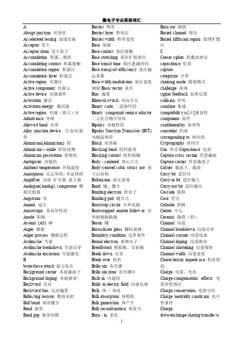
微电子专业英语词汇
AAbruptjunctio n 突变结Acceler ated testing加速实验Accepto r 受主Accepto r atom 受主原子Accumul ation积累、堆积Accumul atingcontact积累接触Accumul ationregion积累区Accumul ationlayer 积累层Activeregion有源区Activecompone nt 有源元Activedevice有源器件Activat ion 激活Activat ion energy激活能Activeregion有源(放大)区Admitta nce 导纳Allowed band 允带Alloy-junctio n device合金结器件Aluminu m(Alumini um) 铝Aluminu m – oxide 铝氧化物Aluminu m passiva tion 铝钝化Ambipol ar 双极的Ambient tempera ture 环境温度Amorpho us 无定形的,非晶体的Amplifi er 功放扩音器放大器Analogu e(Analog)compara tor 模拟比较器Angstro m 埃Anneal退火Anisotr opic 各向异性的Anode 阳极Arsenic (AS) 砷Auger 俄歇Auger process俄歇过程Avalanc he 雪崩Avalanc he breakdo wn 雪崩击穿Avalanc he excitat ion 雪崩激发Bbrute-force attack强力攻击Backgro und carrier本底载流子Backgro und doping本底掺杂Backwar d 反向Backwar d bias 反向偏置Ballast ing resisto r 整流电阻Ball bond 球形键合Band 能带Band gap 能带间隙Barrier势垒Barrier layer 势垒层Barrier width 势垒宽度Base 基极Base contact基区接触Base stretch ing 基区扩展效应Base transit time 基区渡越时间Base transpo rt efficie ncy 基区输运系数Base-width modulat ion 基区宽度调制Basis vector基矢Bias 偏置Bilater al switch双向开关Binarycode 二进制代码Binarycompoun d semicon ductor二元化合物半导体Bipolar双极性的Bipolar Junctio n Transis tor (BJT)双极晶体管Bloch 布洛赫Blockin g band 阻挡能带Blockin g contact阻挡接触Body - centere d 体心立方Body-centred cubic structu re 体立心结构Boltzma nn 波尔兹曼Bond 键、键合Bonding electro n 价电子Bonding pad 键合点Bootstr ap circuit自举电路Bootstr appedemitter followe r 自举射极跟随器Boron 硼Borosil icateglass 硼硅玻璃Boundar y conditi on 边界条件Bound electro n 束缚电子Breadbo ard 模拟板、实验板Break down 击穿Break over 转折Brillou in 布里渊Brillou in zone 布里渊区Built-in 内建的Build-in electri c field 内建电场Bulk 体/ 体内Bulk absorpt ion 体吸收Bulk generat ion 体产生Bulk recombi nation体复合Burn - in 老化Burn out 烧毁Buriedchannel埋沟Burieddiffusi on region隐埋扩散区CCaesarcipher凯撒加密法capacit ance 电容capturecategor ize 分类chainin g mode 链接模式challen ge 质询cipherfeedbac k 加密反馈collisi on 冲突combine集成compati bility n.[计]兼容性compone nt 原件confide ntiali ty 保密性constra int 约束corresp onding to 相应的Cryptog raphy密码学Can 外壳 Capacit ance 电容Capture cross section俘获截面Capture carrier俘获载流子Carrier载流子、载波Carry bit 进位位Carry-in bit 进位输入Carry-out bit 进位输出Cascade级联Case 管壳Cathode阴极Center中心Ceramic陶瓷(的)Channel沟道Channel breakdo wn 沟道击穿Channel current沟道电流Channel doping沟道掺杂Channel shorten ing 沟道缩短Channel width 沟道宽度Charact eristi c impedan ce 特征阻抗Charge电荷、充电Charge-compens ationeffects电荷补偿效应Chargeconserv ation电荷守恒Chargeneutral ity conditi on 电中性条件Chargedrive/exchang e/sharing/transfe r/st1orage电荷驱动/ 交换/ 共享/ 转移/ 存储Chemmic al etching化学腐蚀法Chemica lly-Polish化学抛光Chemmic ally-Mechani callyPolish(CMP) 化学机械抛光Chip 芯片Chip yield 芯片成品率Clamped箝位Clampin g diode 箝位二极管Cleavag e plane 解理面Clock rate 时钟频率Clock generat or 时钟发生器Clock flip-flop 时钟触发器Close-packedstructu re 密堆积结构Close-loop gain 闭环增益Collect or 集电极Collisi on 碰撞Compens ated OP-AMP 补偿运放Common-base/collect or/emitter connect ion 共基极/ 集电极/ 发射极连接Common-gate/drain/sourceconnect ion 共栅/ 漏/ 源连接Common-mode gain 共模增益Common-mode input 共模输入Common-mode rejecti on ratio (CMRR) 共模抑制比Compati bility兼容性Compens ation补偿Compens ated impurit ies 补偿杂质Compens ated semicon ductor补偿半导体Complem entary Darling ton circuit 互补达林顿电路Complem entaryMetal-Oxide-Semicon ductor Field-Effect-Transis tor(CMOS)互补金属氧化物半导体场效应晶体管Complem entary error functio n 余误差函数Compoun d Semicon ductor化合物半导体Conduct ance 电导Conduct ion band (edge) 导带( 底) Conduct ion level/state 导带态Conduct or 导体Conduct ivity电导率Configu ration组态Conlomb库仑Conpled Configu ration Devices结构组态 Constan ts 物理常数Constan t energysurface等能面Constan t-sourcediffusi on 恒定源扩散Contact接触Contami nation治污Continu ity equatio n 连续性方程Contact hole 接触孔Contact potenti al 接触电势Continu ity conditi on 连续性条件Contradoping反掺杂Control led 受控的Convert er 转换器Conveye r 传输器Copperinterco nnecti on system铜互连系统Couping耦合Covalen t 共阶的Crossov er 跨交Critica l 临界的Crossun der 穿交Crucibl e 坩埚Crystaldefect/face/orienta tion/lattice晶体缺陷/ 晶面/ 晶向/ 晶格Current density电流密度Curvatu re 曲率Cut off 截止Current drift/dirve/sharing电流漂移/ 驱动/ 共享Current Sense 电流取样Curvatu re 弯曲Customintegra ted circuit定制集成电路Cylindr ical 柱面的Czochra lshicr ystal直立单晶Czochra lski techniq ue 切克劳斯基技术(Cz 法直拉晶体J )Ddedicat e 专用的,单一的denialof service(DOS)拒绝服务攻击diffusi on 扩散digital signatu re algorit hm 数字签名算法dynamic动态的Danglin g bonds 悬挂键Dark current暗电流Dead time 空载时间Debye length德拜长度De.broglie德布洛意Decdera te 减速Decibel (dB) 分贝Decode译码Deep accepto r level 深受主能级Deep donor level 深施主能级Deep impurit y level 深度杂质能级Deep trap 深陷阱Defeat缺陷Degener ate semicon ductor简并半导体 Degener acy 简并度Degrada tion 退化DegreeCelsius(centigr ade)/Kelvin摄氏/ 开氏温度Delay 延迟Density密度Density of states态密度Depleti on 耗尽Depleti on approxi mation耗尽近似Depleti on contact耗尽接触Depleti on depth 耗尽深度Depleti on effect耗尽效应Depleti on layer 耗尽层Depleti on MOS 耗尽MOSDepleti on region耗尽区Deposit ed film 淀积薄膜Deposit ion process淀积工艺Designrules 设计规则Die 芯片(复数dice )Diode 二极管Dielect ric 介电的Dielect ric isolati on 介质隔离Differe nce-mode input 差模输入Differe ntialamplifi er 差分放大器Differe ntialcapacit ance 微分电容Diffuse d junctio n 扩散结Diffusi on 扩散2Diffusi on coeffic ient 扩散系数Diffusi on constan t 扩散常数Diffusi vity 扩散率Diffusi oncapacit ance/barrier/current/furnace 扩散电容/ 势垒/ 电流/ 炉Digital circuit数字电路Dipoledomain偶极畴Dipolelayer 偶极层Direct-couplin g 直接耦合Direct-gap semicon ductor直接带隙半导体Directtransit ion 直接跃迁Dischar ge 放电Discret e compone nt 分立元件Dissipa tion 耗散Distrib ution分布Distrib uted capacit ance 分布电容istribu ted model 分布模型Displac ement位移Disloca tion 位错Domain畴Donor 施主Donor exhaust ion 施主耗尽Dopant掺杂剂Doped semicon ductor掺杂半导体oping concent ration掺杂浓度Double-diffusi ve MOS(DMOS) 双扩散MOS. Drift 漂移Drift field 漂移电场Drift mobilit y 迁移率Dry etching干法腐蚀Dry/wet oxidati on 干/ 湿法氧化Dose 剂量Duty cycle 工作周期Dual-in-line package(DIP )双列直插式封装Dynamic s 动态Dynamic charact eristi cs 动态属性Dynamic impedan ce 动态阻抗Eexperti se 专长extract orEarly effect厄利效应Early failure早期失效Effecti ve mass 有效质量Einstei n relatio n(ship) 爱因斯坦关系Electri c Erase Program mableRead Only Memory(E2PROM)一次性电可擦除只读存储器Electro de 电极Electro minggr atim 电迁移Electro n affinit y 电子亲和势Electro nic -grade 电子能Electro n-beam photo-resistexposur e 光致抗蚀剂的电子束曝光Electro n gas 电子气Electro n-grade water 电子级纯水Electro n trappin g center电子俘获中心Electro n V olt (eV) 电子伏Electro static静电的Element元素/ 元件/ 配件Element al semicon ductor元素半导体 Ellipse椭圆Ellipso id 椭球Emitter发射极Emitter-coupled logic 发射极耦合逻辑Emitter-coupled pair 发射极耦合对Emitter followe r 射随器Empty band 空带Emitter crowdin g effect发射极集边(拥挤)效应Enduran ce test =life test 寿命测试Energystate 能态Energymomentu m diagram能量- 动量(E-K) 图Enhance ment mode 增强型模式Enhance ment MOS 增强性MOS Entefic ( 低) 共溶的Environ mental test 环境测试Epitaxi al 外延的Epitaxi al layer 外延层Epitaxi al slice 外延片Expitax y 外延Equival ent curcuit等效电路Equilib rium majorit y /minorit ycarrier s 平衡多数/ 少数载流子Erasabl e Program mableROM(EPROM) 可搽取(编程)存储器Error functio n complem ent 余误差函数Etch 刻蚀Etchant刻蚀剂Etching mask 抗蚀剂掩模Excesscarrier过剩载流子Excitat ion energy激发能Excited state 激发态Exciton激子Extrapo lation外推法Extrins ic 非本征的Extrins ic semicon ductor杂质半导体Ffabrica tion伪造fleshed outFace - centere d 面心立方Fall time 下降时间Fan-in 扇入Fan-out 扇出Fast recover y 快恢复Fast surface states快界面态Feedbac k 反馈Fermi level 费米能级Fermi-Dirac Distrib ution费米-狄拉克布Femi potenti al 费米势Fick equatio n 菲克方程(扩散)Field effecttransis tor 场效应晶体管Field oxide 场氧化层Filledband 满带Film 薄膜Flash memory闪烁存储器Flat band 平带Flat pack 扁平封装Flicker noise 闪烁(变)噪声Flip-flop toggle触发器翻转Floatin g gate 浮栅Fluorid e etch 氟化氢刻蚀Forbidd en band 禁带Forward bias 正向偏置Forward blockin g /conduct ing 正向阻断/ 导通Frequen cy deviati on noise 频率3漂移噪声Frequen cy respons e 频率响应Functio n 函数GgridGain 增益Gallium-Arsenid e(GaAs) 砷化钾Gamy ray r 射线Gate 门、栅、控制极Gate oxide 栅氧化层Gauss (ian )高斯Gaussia n distrib utionprofile高斯掺杂分布Generat ion-recombi nation产生- 复合Geometr ies 几何尺寸Germani um(Ge) 锗Graded缓变的Graded(gradual) channel缓变沟道Gradedjunctio n 缓变结Grain 晶粒Gradien t 梯度Grown junctio n 生长结Guard ring 保护环Gummel-Poom model 葛谋- 潘模型Gunn - effect狄氏效应Hhandle处理hierarc hical层次Hardene d device辐射加固器件Heat of formati on 形成热Heat sink 散热器、热沉Heavy/light hole band 重/轻空穴带Heavy saturat ion 重掺杂Hell - effect霍尔效应Heteroj unctio n 异质结Heteroj unctio n structu re 异质结结构Heteroj unctio n Bipolar Transis tor (HBT )异质结双极型晶体High field propert y 高场特性High-perform ance MOS.( H-MOS) 高性能MOS.Hormali zed 归一化Horizon tal epitaxi al reactor卧式外延反应器Hot carrior热载流子Hybridintegra tion 混合集成Iimpleme ntinducta nce 电感initial izatio n vectorIV初始化向量integri ty完整性interce ption截获interru ption中断Image - force 镜象力Impactionizat ion 碰撞电离Impedan ce 阻抗Imperfe ct structu re 不完整结构Implant ationdose 注入剂量Implant ed ion 注入离子Impurit y 杂质Impurit y scatter ing 杂志散射Increme ntal resista nce 电阻增量(微分电阻)In-contact mask 接触式掩模Indiumtin oxide (ITO) 铟锡氧化物 Induced channel感应沟道Infrare d 红外的Injecti on 注入Input offsetvoltage输入失调电压Insulat or 绝缘体Insulat ed Gate FET(IGFET) 绝缘栅FET Integra ted injecti on logic 集成注入逻辑Integra tion 集成、积分Interco nnecti on 互连Interco nnecti on time delay 互连延时Interdi gitate d structu re 交互式结构Interfa ce 界面Interfe rence干涉Interna tional systemof unions国际单位制Interna lly scatter ing 谷间散射Interpo lation内插法Intrins ic 本征的Intrins ic semicon ductor本征半导体 Inverse operati on 反向工作Inversi on 反型Inverte r 倒相器Ion 离子Ion beam 离子束Ion etching离子刻蚀Ion implant ation离子注入Ionizat ion 电离Ionizat ion energy电离能Irradia tion 辐照Isolati on land 隔离岛Isotrop ic 各向同性Jjava appletJava小程序Junctio n FET(JFET) 结型场效应管Junctio n isolati on 结隔离Junctio n spacing结间距Junctio n side-wall 结侧壁Kkey wrappin g 密钥包装LLatch up 闭锁Lateral横向的Lattice晶格Layout版图Latticebinding/cell/constan t/defect/distortion 晶格结合力/ 晶胞/ 晶格/ 晶格常熟/ 晶格缺陷/ 晶格畸变Leakage current(泄)漏电流Level shiftin g 电平移动Life time 寿命lineari ty 线性度Linkedbond 共价键LiquidNitroge n 液氮Liquid-phase epitaxi al growthtechniq ue 液相外延生长技术Lithogr aphy 光刻Light Emittin g Diode(LED) 发光二极管Load line or Variabl e 负载线Locatin g and Wiring布局布线Longitu dinal纵向的Logic swing 逻辑摆幅Lorentz洛沦兹Lumpedmodel 集总模型4Mmasquer ade伪装message digest消息摘要modific ation修改multidr op 多站, 多支路Majorit y carrier多数载流子Mask 掩膜板,光刻板Mask level 掩模序号Mask set 掩模组Mass - actionlaw 质量守恒定律Master-slave D flip-flop 主从 D 触发器Matchin g 匹配Maxwell麦克斯韦Mean free path 平均自由程Meander ed emitter junctio n 梳状发射极结Mean time beforefailure (MTBF) 平均工作时间Megeto- resista nce 磁阻Mesa 台面MESFET-Metal Semicon ductor 金属半导体FETMetalli zation金属化Microel ectron ic techniq ue 微电子技术Microel ectron ics 微电子学Millenindices密勒指数Minorit y carrier少数载流子Misfit失配Mismatc hing 失配Mobileions 可动离子Mobilit y 迁移率Module模块Modulat e 调制Molecul ar crystal分子晶体Monolit hic IC 单片IC MOSFET金属氧化物半导体场效应晶体管Mos. Transis tor(MOST )MOS. 晶体管 Multipl icatio n 倍增Modulat or 调制Multi-chip IC 多芯片ICMulti-chip module(MCM) 多芯片模块Multipl icatio n coeffic ient 倍增因子Nnetwork level attack网络层攻击non-repudia tion 不可抵赖Naked chip 未封装的芯片(裸片)Negativ e feedbac k 负反馈Negativ e resista nce 负阻Nesting套刻Negativ e-tempera ture-coeffic ient负温度系数Noise margin噪声容限Nonequi libriu m 非平衡Nonrola tile 非挥发(易失)性Normall y off/on 常闭/ 开Numeric al analysi s 数值分析Ooptimiz e 使最优化Occupie d band 满带Officie nay 功率Offset偏移、失调On standby待命状态Ohmic contact欧姆接触Open circuit开路Operati ng point 工作点Operati ng bias 工作偏置Operati onal amplifi er (OPAMP)运算放大器Optical photon=photon光子Optical quenchi ng 光猝灭Optical transit ion 光跃迁Optical-coupled isolato r 光耦合隔离器Organic semicon ductor有机半导体Orienta tion 晶向、定向Outline外形Out-of-contact mask 非接触式掩模Outputcharact eristi c 输出特性Outputvoltage swing 输出电压摆幅Overcom pensat ion 过补偿Over-current protect ion 过流保护Over shoot 过冲Over-voltage protect ion 过压保护Overlap交迭Overloa d 过载Oscilla tor 振荡器Oxide 氧化物Oxidati on 氧化Oxide passiva tion 氧化层钝化Pparalle lparasit ic 寄生的partiti on [简明英汉词典]n.分割,划分, 瓜分, 分开, 隔离物vt.区分, 隔开, 分割present ationn.介绍, 陈述, 赠送,表达primiti veprivateprobabl yproceed ingprofoun dpropert ypseudoc ollisi on伪冲突Package封装Pad 压焊点Paramet er 参数Parasit ic effect寄生效应Parasit ic oscilla tion 寄生振荡Passina tion 钝化Passive compone nt 无源元件Passive device无源器件Passive surface钝化界面Parasit ic transis tor 寄生晶体管Peak-point voltage峰点电压Peak voltage峰值电压Permane nt-storage circuit永久存储电路Period周期Periodi c table 周期表Permeab le - base 可渗透基区Phase-lock loop 锁相环Phase drift 相移Phononspectra声子谱Photo conduct ion 光电导Photo diode 光电二极管Photoel ectric cell 光电池Photoel ectric effect光电效应Photoen ic devices光子器件Photoli thogra phic process光刻工艺(photo) resist(光敏)抗腐蚀剂Pin 管脚Pinch off 夹断5Pinning of Fermi level 费米能级的钉扎(效应)Planarprocess平面工艺Planartransis tor 平面晶体管Plasma等离子体Plezoel ec tric effect压电效应Poisson equatio n 泊松方程Point contact点接触Polarit y 极性Polycry stal 多晶Polymer semicon ductor聚合物半导体Poly-silicon多晶硅Potenti al ( 电) 势Potenti al barrier势垒Potenti al well 势阱Power dissipa tion 功耗Power transis tor 功率晶体管Preampl ifier前置放大器Primary flat 主平面Princip al axes 主轴Print-circuit board(PCB) 印制电路板Probabi lity 几率Probe 探针Process工艺Propaga tion delay 传输延时Pseudop otenti al method膺势发Punch through穿通Pulse trigger ing/modulat ing 脉冲触发/ 调制Pulse Widen Modulat or(PWM) 脉冲宽度调制Punchth rough穿通Push-pull stage 推挽级QQuality factor品质因子Quantiz ation量子化Quantum量子Quantum efficie ncy 量子效应Quantum mechani cs 量子力学Quasi –Fermi -level 准费米能级Quartz石英Rrelease of message content s发布消息内容registe r 寄存器registr ation注册, 报到, 登记resista nce 电阻routingrunning key cipher运动密钥加密法Radiati on conduct ivity辐射电导率Radiati on damage辐射损伤Radiati on flux density辐射通量密度Radiati on hardeni ng 辐射加固Radiati on protect ion 辐射保护Radiati ve - recombi nation辐照复合Radioac tive 放射性Reach through穿通Reactiv e sputter ing source反应溅射源Read diode 里德二极管Recombi nation复合Recover y diode 恢复二极管Recipro cal lattice倒核子Recover y time 恢复时间Rectifi er 整流器(管)Rectify ing contact整流接触Referen ce 基准点基准参考点Refract ive index 折射率Registe r 寄存器Registr ation对准Regulat e 控制调整Relaxat ion lifetim e 驰豫时间Reliabi lity 可*性Resonan ce 谐振Resista nce 电阻Resisto r 电阻器Resisti vity 电阻率Regulat or 稳压管(器)Relaxat ion 驰豫Resonan t frequen cy 共射频率Respons e time 响应时间Reverse反向的Reverse bias 反向偏置Sscratchscratch pad缓存secret密钥substra te 衬底synchro nizesynthes izesymmetr ic key cryptog raphy对称密钥加密sophist icate复杂的suspend悬挂,延缓Samplin g circuit取样电路Sapphir e 蓝宝石(Al2O3 )Satelli te valley卫星谷Saturat ed current range 电流饱和区Saturat ion region饱和区Saturat ion 饱和的Scaleddown 按比例缩小Scatter ing 散射Schockl ey diode 肖克莱二极管Schottk y 肖特基Schottk y barrier肖特基势垒Schottk y contact肖特基接触Schrodi ngen 薛定厄Scribin g grid 划片格Seconda ry flat 次平面Seed crystal籽晶Segrega tion 分凝Selecti vity 选择性Self aligned自对准的Self diffusi on 自扩散Semicon ductor半导体Semicon ductor-control led rectifi er可控硅Sendsit ivity灵敏度Serial串行/ 串联Seriesinducta nce 串联电感Settletime 建立时间Sheet resista nce 薄层电阻Shield屏蔽Short circuit短路Shot noise 散粒噪声Shunt 分流Sidewal l capacit ance 边墙电容Signal信号Silicaglass 石英玻璃Silicon硅Silicon carbide碳化硅Silicon dioxide (SiO2) 二氧化硅Silicon Nitride(Si3N4) 氮化硅Silicon On Insulat or 绝缘硅Siliver whisker s 银须Simplecubic 简立方6Singlecrystal单晶Sink 沉Skin effect趋肤效应Snap time 急变时间Sneak path 潜行通路Sulethr eshold亚阈的Solar battery/cell 太阳能电池Solid circuit固体电路Solid Solubil ity 固溶度Sonband子带Source源极Sourcefollowe r 源随器Space charge空间电荷Specifi c heat(PT) 热Speed-power product速度功耗乘积Spheric al 球面的Spin 自旋Split 分裂Spontan eous emissio n 自发发射Spreadi ng resista nce 扩展电阻Sputter溅射Stackin g fault 层错Staticcharact eristi c 静态特性Stimula ted emissio n 受激发射Stimula ted recombi nation受激复合Storage time 存储时间Stress应力Straggl e 偏差Sublima tion 升华Substra te 衬底Substit utiona l 替位式的Superla ttice超晶格Supply电源Surface表面Surge capacit y 浪涌能力Subscri pt 下标Switchi ng time 开关时间Switch开关Ttoken 令牌trace 追溯traffic analysi s 分析通信量Trojanhorse 特洛伊木马Tailing扩展Termina l 终端Tensor张量Tensori al 张量的Thermal activat ion 热激发Thermal conduct ivity热导率Thermal equilib rium 热平衡Thermal Oxidati on 热氧化Thermal resista nce 热阻Thermal sink 热沉Thermal velocit y 热运动Thermoe lectri cpovoe r 温差电动势率Thick-film techniq ue 厚膜技术Thin-film hybridIC 薄膜混合集成电路Thin-Film Transis tor(TFT) 薄膜晶体 Threshl od 阈值Thyisto r 晶闸管Transco nducta nce 跨导Transfe r charact eristi c 转移特性Transfe r electro n 转移电子Transfe r functio n 传输函数Transie nt 瞬态的Transis tor aging(stress)晶体管老化Transit time 渡越时间Transit ion 跃迁Transit ion-metal silica过度金属硅化物Transit ion probabi lity 跃迁几率Transit ion region过渡区Transpo rt 输运Transve rse 横向的Trap 陷阱Trappin g 俘获Trapped charge陷阱电荷Triangl e generat or 三角波发生器Triboel ectric ity 摩擦电Trigger触发Trim 调配调整Triplediffusi on 三重扩散Truth table 真值表Tolerah ce 容差Tunnel(ing) 隧道(穿)Tunnelcurrent隧道电流Turn over 转折Turn - off time 关断时间UUltravi olet 紫外的Unijunc tion 单结的Unipola r 单极的Unit cell 原(元)胞Unity-gain frequen cy 单位增益频率Unilate ral-switch单向开关Vvarietyvectorverify检验victoryvertica lvia 通孔virus病毒Vacancy空位Vacuum真空Valence(value) band 价带V alue band edge 价带顶Valence bond 价键Vapourphase 汽相Varacto r 变容管Varisto r 变阻器Vibrati on 振动Voltage电压WWorm 蠕虫Wafer 晶片Wave equatio n 波动方程Wave guide 波导Wave number波数Wave-particl e duality波粒二相性Wear-out 烧毁Wire routing布线Work functio n 功函数Worst-case device最坏情况器件YYield 成品率ZZener breakdo wn 齐纳击穿Zone melting区熔法7。
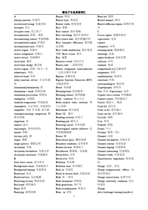
微电子专业英语词汇
AAbrupt junction 突变结Accelerated testing 加速实验Acceptor 受主Acceptor atom 受主原子Accumulation 积累、堆积Accumulating contact 积累接触Accumulation region 积累区Accumulation layer 积累层Active region 有源区Active component 有源元Active device 有源器件Activation 激活Activation energy 激活能Active region 有源(放大)区Admittance 导纳Allowed band 允带Alloy-junction device 合金结器件Aluminum(Aluminium) 铝Aluminum – oxide 铝氧化物Aluminum passivation 铝钝化Ambipolar 双极的Ambient temperature 环境温度Amorphous 无定形的,非晶体的Amplifier 功放扩音器放大器Analogue(Analog) comparator 模拟比较器Angstrom 埃Anneal 退火Anisotropic 各向异性的Anode 阳极Arsenic (AS) 砷Auger 俄歇Auger process 俄歇过程Avalanche 雪崩Avalanche breakdown 雪崩击穿Avalanche excitation 雪崩激发Bbrute-force attack 强力攻击Background carrier 本底载流子Background doping 本底掺杂Backward 反向Backward bias 反向偏置Ballasting resistor 整流电阻Ball bond 球形键合Band 能带Band gap 能带间隙Barrier 势垒Barrier layer 势垒层Barrier width 势垒宽度Base 基极Base contact 基区接触Base stretching 基区扩展效应Base transit time 基区渡越时间Base transport efficiency 基区输运系数Base-width modulation 基区宽度调制Basis vector 基矢Bias 偏置Bilateral switch 双向开关Binary code 二进制代码Binary compound semiconductor二元化合物半导体Bipolar 双极性的Bipolar Junction Transistor (BJT)双极晶体管Bloch 布洛赫Blocking band 阻挡能带Blocking contact 阻挡接触Body - centered 体心立方Body-centred cubic structure 体立心结构Boltzmann 波尔兹曼Bond 键、键合Bonding electron 价电子Bonding pad 键合点Bootstrap circuit 自举电路Bootstrapped emitter follower 自举射极跟随器Boron 硼Borosilicate glass 硼硅玻璃Boundary condition 边界条件Bound electron 束缚电子Breadboard 模拟板、实验板Break down 击穿Break over 转折Brillouin 布里渊Brillouin zone 布里渊区Built-in 内建的Build-in electric field 内建电场Bulk 体/ 体内Bulk absorption 体吸收Bulk generation 体产生Bulk recombination 体复合Burn - in 老化Burn out 烧毁Buried channel 埋沟Buried diffusion region 隐埋扩散区CCaesar cipher 凯撒加密法capacitance 电容capturecategorize 分类chaining mode 链接模式challenge 质询cipher feedback 加密反馈collision 冲突combine 集成compatibility n.[计]兼容性component 原件confidentiality 保密性constraint 约束corresponding to 相应的Cryptography 密码学Can 外壳Capacitance 电容Capture cross section 俘获截面Capture carrier 俘获载流子Carrier 载流子、载波Carry bit 进位位Carry-in bit 进位输入Carry-out bit 进位输出Cascade 级联Case 管壳Cathode 阴极Center 中心Ceramic 陶瓷(的)Channel 沟道Channel breakdown 沟道击穿Channel current 沟道电流Channel doping 沟道掺杂Channel shortening 沟道缩短Channel width 沟道宽度Characteristic impedance 特征阻抗Charge 电荷、充电Charge-compensation effects 电荷补偿效应Charge conservation 电荷守恒Charge neutrality condition 电中性条件Chargedrive/exchange/sharing/transfer/st1orage 电荷驱动/ 交换/ 共享/ 转移/ 存储Chemmical etching 化学腐蚀法Chemically-Polish 化学抛光Chemmically-Mechanically Polish (CMP) 化学机械抛光Chip 芯片Chip yield 芯片成品率Clamped 箝位Clamping diode 箝位二极管Cleavage plane 解理面Clock rate 时钟频率Clock generator 时钟发生器Clock flip-flop 时钟触发器Close-packed structure 密堆积结构Close-loop gain 闭环增益Collector 集电极Collision 碰撞Compensated OP-AMP 补偿运放Common-base/collector/emitter connection 共基极/ 集电极/ 发射极连接Common-gate/drain/source connection 共栅/ 漏/ 源连接Common-mode gain 共模增益Common-mode input 共模输入Common-mode rejection ratio (CMRR) 共模抑制比Compatibility 兼容性Compensation 补偿Compensated impurities 补偿杂质Compensated semiconductor 补偿半导体Complementary Darlington circuit 互补达林顿电路ComplementaryMetal-Oxide-Semiconductor Field-Effect-Transistor(CMOS)互补金属氧化物半导体场效应晶体管Complementary error function 余误差函数Compound Semiconductor 化合物半导体Conductance 电导Conduction band (edge) 导带( 底) Conduction level/state 导带态Conductor 导体Conductivity 电导率Configuration 组态Conlomb 库仑Conpled Configuration Devices结构组态Constants 物理常数Constant energy surface 等能面Constant-source diffusion 恒定源扩散Contact 接触Contamination 治污Continuity equation 连续性方程Contact hole 接触孔Contact potential 接触电势Continuity condition 连续性条件Contra doping 反掺杂Controlled 受控的Converter 转换器Conveyer 传输器Copper interconnection system 铜互连系统Couping 耦合Covalent 共阶的Crossover 跨交Critical 临界的Crossunder 穿交Crucible 坩埚Crystaldefect/face/orientation/lattice 晶体缺陷/ 晶面/ 晶向/ 晶格Current density 电流密度Curvature 曲率Cut off 截止Current drift/dirve/sharing 电流漂移/ 驱动/ 共享Current Sense 电流取样Curvature 弯曲Custom integrated circuit 定制集成电路Cylindrical 柱面的Czochralshicrystal 直立单晶Czochralski technique 切克劳斯基技术(Cz 法直拉晶体J )Ddedicate 专用的,单一的denial of service(DOS)拒绝服务攻击diffusion 扩散digital signature algorithm 数字签名算法dynamic 动态的Dangling bonds 悬挂键Dark current 暗电流Dead time 空载时间Debye length 德拜长度De.broglie 德布洛意Decderate 减速Decibel (dB) 分贝Decode 译码Deep acceptor level 深受主能级Deep donor level 深施主能级Deep impurity level 深度杂质能级Deep trap 深陷阱Defeat 缺陷Degenerate semiconductor 简并半导体Degeneracy 简并度Degradation 退化Degree Celsius(centigrade)/Kelvin 摄氏/ 开氏温度Delay 延迟Density 密度Density of states 态密度Depletion 耗尽Depletion approximation 耗尽近似Depletion contact 耗尽接触Depletion depth 耗尽深度Depletion effect 耗尽效应Depletion layer 耗尽层Depletion MOS 耗尽MOSDepletion region 耗尽区Deposited film 淀积薄膜Deposition process 淀积工艺Design rules 设计规则Die 芯片(复数dice )Diode 二极管Dielectric 介电的Dielectric isolation 介质隔离Difference-mode input 差模输入Differential amplifier 差分放大器Differential capacitance 微分电容Diffused junction 扩散结Diffusion 扩散2Diffusion coefficient 扩散系数Diffusion constant 扩散常数Diffusivity 扩散率Diffusioncapacitance/barrier/current/furnac e 扩散电容/ 势垒/ 电流/ 炉Digital circuit 数字电路Dipole domain 偶极畴Dipole layer 偶极层Direct-coupling 直接耦合Direct-gap semiconductor 直接带隙半导体Direct transition 直接跃迁Discharge 放电Discrete component 分立元件Dissipation 耗散Distribution 分布Distributed capacitance 分布电容istributed model 分布模型Displacement 位移Dislocation 位错Domain 畴Donor 施主Donor exhaustion 施主耗尽Dopant 掺杂剂Doped semiconductor 掺杂半导体oping concentration 掺杂浓度Double-diffusive MOS(DMOS) 双扩散MOS. Drift 漂移Drift field 漂移电场Drift mobility 迁移率Dry etching 干法腐蚀Dry/wet oxidation 干/ 湿法氧化Dose 剂量Duty cycle 工作周期Dual-in-line package (DIP )双列直插式封装Dynamics 动态Dynamic characteristics 动态属性Dynamic impedance 动态阻抗Eexpertise 专长extractorEarly effect 厄利效应Early failure 早期失效Effective mass 有效质量Einstein relation(ship) 爱因斯坦关系Electric Erase ProgrammableRead Only Memory(E2PROM)一次性电可擦除只读存储器Electrode 电极Electrominggratim 电迁移Electron affinity 电子亲和势Electronic -grade 电子能Electron-beam photo-resistexposure 光致抗蚀剂的电子束曝光Electron gas 电子气Electron-grade water 电子级纯水Electron trapping center 电子俘获中心Electron V olt (eV) 电子伏Electrostatic 静电的Element 元素/ 元件/ 配件Elemental semiconductor 元素半导体Ellipse 椭圆Ellipsoid 椭球Emitter 发射极Emitter-coupled logic 发射极耦合逻辑Emitter-coupled pair 发射极耦合对Emitter follower 射随器Empty band 空带Emitter crowding effect 发射极集边(拥挤)效应Endurance test =life test 寿命测试Energy state 能态Energy momentum diagram 能量- 动量(E-K) 图Enhancement mode 增强型模式Enhancement MOS 增强性MOS Entefic ( 低) 共溶的Environmental test 环境测试Epitaxial 外延的Epitaxial layer 外延层Epitaxial slice 外延片Expitaxy 外延Equivalent curcuit 等效电路Equilibrium majority /minoritycarriers 平衡多数/ 少数载流子Erasable Programmable ROM(EPROM) 可搽取(编程)存储器Error function complement 余误差函数Etch 刻蚀Etchant 刻蚀剂Etching mask 抗蚀剂掩模Excess carrier 过剩载流子Excitation energy 激发能Excited state 激发态Exciton 激子Extrapolation 外推法Extrinsic 非本征的Extrinsic semiconductor 杂质半导体Ffabrication伪造fleshed outFace - centered 面心立方Fall time 下降时间Fan-in 扇入Fan-out 扇出Fast recovery 快恢复Fast surface states 快界面态Feedback 反馈Fermi level 费米能级Fermi-Dirac Distribution 费米-狄拉克布Femi potential 费米势Fick equation 菲克方程(扩散)Field effect transistor 场效应晶体管Field oxide 场氧化层Filled band 满带Film 薄膜Flash memory 闪烁存储器Flat band 平带Flat pack 扁平封装Flicker noise 闪烁(变)噪声Flip-flop toggle 触发器翻转Floating gate 浮栅Fluoride etch 氟化氢刻蚀Forbidden band 禁带Forward bias 正向偏置Forward blocking /conducting 正向阻断/ 导通Frequency deviation noise 频率3漂移噪声Frequency response 频率响应Function 函数GgridGain 增益Gallium-Arsenide(GaAs) 砷化钾Gamy ray r 射线Gate 门、栅、控制极Gate oxide 栅氧化层Gauss (ian )高斯Gaussian distribution profile 高斯掺杂分布Generation-recombination 产生- 复合Geometries 几何尺寸Germanium(Ge) 锗Graded 缓变的Graded (gradual) channel 缓变沟道Graded junction 缓变结Grain 晶粒Gradient 梯度Grown junction 生长结Guard ring 保护环Gummel-Poom model 葛谋- 潘模型Gunn - effect 狄氏效应Hhandle 处理hierarchical 层次Hardened device 辐射加固器件Heat of formation 形成热Heat sink 散热器、热沉Heavy/light hole band 重/轻空穴带Heavy saturation 重掺杂Hell - effect 霍尔效应Heterojunction 异质结Heterojunction structure 异质结结构Heterojunction Bipolar Transistor (HBT )异质结双极型晶体High field property 高场特性High-performance MOS.( H-MOS) 高性能MOS.Hormalized 归一化Horizontal epitaxial reactor 卧式外延反应器Hot carrior 热载流子Hybrid integration 混合集成Iimplementinductance 电感initialization vector IV初始化向量integrity完整性interception 截获interruption中断Image - force 镜象力Impact ionization 碰撞电离Impedance 阻抗Imperfect structure 不完整结构Implantation dose 注入剂量Implanted ion 注入离子Impurity 杂质Impurity scattering 杂志散射Incremental resistance 电阻增量(微分电阻)In-contact mask 接触式掩模Indium tin oxide (ITO) 铟锡氧化物Induced channel 感应沟道Infrared 红外的Injection 注入Input offset voltage 输入失调电压Insulator 绝缘体Insulated Gate FET(IGFET) 绝缘栅FET Integrated injection logic 集成注入逻辑Integration 集成、积分Interconnection 互连Interconnection time delay 互连延时Interdigitated structure 交互式结构Interface 界面Interference 干涉International system of unions 国际单位制Internally scattering 谷间散射Interpolation 内插法Intrinsic 本征的Intrinsic semiconductor 本征半导体Inverse operation 反向工作Inversion 反型Inverter 倒相器Ion 离子Ion beam 离子束Ion etching 离子刻蚀Ion implantation 离子注入Ionization 电离Ionization energy 电离能Irradiation 辐照Isolation land 隔离岛Isotropic 各向同性Jjava applet Java小程序Junction FET(JFET) 结型场效应管Junction isolation 结隔离Junction spacing 结间距Junction side-wall 结侧壁Kkey wrapping 密钥包装LLatch up 闭锁Lateral 横向的Lattice 晶格Layout 版图Latticebinding/cell/constant/defect/distortion 晶格结合力/ 晶胞/ 晶格/ 晶格常熟/ 晶格缺陷/ 晶格畸变Leakage current (泄)漏电流Level shifting 电平移动Life time 寿命linearity 线性度Linked bond 共价键Liquid Nitrogen 液氮Liquid -phase epitaxial growthtechnique 液相外延生长技术Lithography 光刻Light Emitting Diode(LED) 发光二极管Load line or Variable 负载线Locating and Wiring 布局布线Longitudinal 纵向的Logic swing 逻辑摆幅Lorentz 洛沦兹Lumped model 集总模型4Mmasquerade伪装message digest 消息摘要modification 修改multidrop 多站, 多支路Majority carrier 多数载流子Mask 掩膜板,光刻板Mask level 掩模序号Mask set 掩模组Mass - action law 质量守恒定律Master-slave D flip-flop 主从D 触发器Matching 匹配Maxwell 麦克斯韦Mean free path 平均自由程Meandered emitter junction 梳状发射极结Mean time before failure (MTBF) 平均工作时间Megeto - resistance 磁阻Mesa 台面MESFET-Metal Semiconductor 金属半导体FET Metallization 金属化Microelectronic technique 微电子技术Microelectronics 微电子学Millen indices 密勒指数Minority carrier 少数载流子Misfit 失配Mismatching 失配Mobile ions 可动离子Mobility 迁移率Module 模块Modulate 调制Molecular crystal 分子晶体Monolithic IC 单片IC MOSFET 金属氧化物半导体场效应晶体管Mos. Transistor(MOST )MOS. 晶体管Multiplication 倍增Modulator 调制Multi-chip IC 多芯片ICMulti-chip module(MCM) 多芯片模块Multiplication coefficient 倍增因子N network level attack网络层攻击non-repudiation 不可抵赖Naked chip 未封装的芯片(裸片)Negative feedback 负反馈Negative resistance 负阻Nesting 套刻Negative-temperature-coefficient负温度系数Noise margin 噪声容限Nonequilibrium 非平衡Nonrolatile 非挥发(易失)性Normally off/on 常闭/ 开Numerical analysis 数值分析Ooptimize 使最优化Occupied band 满带Officienay 功率Offset 偏移、失调On standby 待命状态Ohmic contact 欧姆接触Open circuit 开路Operating point 工作点Operating bias 工作偏置Operational amplifier (OPAMP)运算放大器Optical photon =photon 光子Optical quenching 光猝灭Optical transition 光跃迁Optical-coupled isolator 光耦合隔离器Organic semiconductor 有机半导体Orientation 晶向、定向Outline 外形Out-of-contact mask 非接触式掩模Output characteristic 输出特性Output voltage swing 输出电压摆幅Overcompensation 过补偿Over-current protection 过流保护Over shoot 过冲Over-voltage protection 过压保护Overlap 交迭Overload 过载Oscillator 振荡器Oxide 氧化物Oxidation 氧化Oxide passivation 氧化层钝化Pparallelparasitic 寄生的partition [简明英汉词典]n.分割,划分, 瓜分, 分开, 隔离物vt.区分, 隔开, 分割presentation n.介绍, 陈述, 赠送,表达primitiveprivateprobablyproceedingprofoundpropertypseudocollision伪冲突Package 封装Pad 压焊点Parameter 参数Parasitic effect 寄生效应Parasitic oscillation 寄生振荡Passination 钝化Passive component 无源元件Passive device 无源器件Passive surface 钝化界面Parasitic transistor 寄生晶体管Peak-point voltage 峰点电压Peak voltage 峰值电压Permanent-storage circuit 永久存储电路Period 周期Periodic table 周期表Permeable - base 可渗透基区Phase-lock loop 锁相环Phase drift 相移Phonon spectra 声子谱Photo conduction 光电导Photo diode 光电二极管Photoelectric cell 光电池Photoelectric effect 光电效应Photoenic devices 光子器件Photolithographic process 光刻工艺(photo) resist (光敏)抗腐蚀剂Pin 管脚5Pinch off 夹断Pinning of Fermi level 费米能级的钉扎(效应)Planar process 平面工艺Planar transistor 平面晶体管Plasma 等离子体Plezoelectric effect 压电效应Poisson equation 泊松方程Point contact 点接触Polarity 极性Polycrystal 多晶Polymer semiconductor 聚合物半导体Poly-silicon 多晶硅Potential ( 电) 势Potential barrier 势垒Potential well 势阱Power dissipation 功耗Power transistor 功率晶体管Preamplifier 前置放大器Primary flat 主平面Principal axes 主轴Print-circuit board(PCB) 印制电路板Probability 几率Probe 探针Process 工艺Propagation delay 传输延时Pseudopotential method 膺势发Punch through 穿通Pulse triggering/modulating 脉冲触发/ 调制Pulse Widen Modulator(PWM) 脉冲宽度调制Punchthrough 穿通Push-pull stage 推挽级QQuality factor 品质因子Quantization 量子化Quantum 量子Quantum efficiency 量子效应Quantum mechanics 量子力学Quasi –Fermi -level 准费米能级Quartz 石英Rrelease of message contents发布消息内容register 寄存器registration 注册, 报到, 登记resistance 电阻routingrunning key cipher 运动密钥加密法Radiation conductivity 辐射电导率Radiation damage 辐射损伤Radiation flux density 辐射通量密度Radiation hardening 辐射加固Radiation protection 辐射保护Radiative - recombination 辐照复合Radioactive 放射性Reach through 穿通Reactive sputtering source 反应溅射源Read diode 里德二极管Recombination 复合Recovery diode 恢复二极管Reciprocal lattice 倒核子Recovery time 恢复时间Rectifier 整流器(管)Rectifying contact 整流接触Reference 基准点基准参考点Refractive index 折射率Register 寄存器Registration 对准Regulate 控制调整Relaxation lifetime 驰豫时间Reliability 可*性Resonance 谐振Resistance 电阻Resistor 电阻器Resistivity 电阻率Regulator 稳压管(器)Relaxation 驰豫Resonant frequency 共射频率Response time 响应时间Reverse 反向的Reverse bias 反向偏置Sscratchscratchpad缓存secret 密钥substrate 衬底synchronizesynthesizesymmetric key cryptography 对称密钥加密sophisticate 复杂的suspend 悬挂,延缓Sampling circuit 取样电路Sapphire 蓝宝石(Al2O3 )Satellite valley 卫星谷Saturated current range 电流饱和区Saturation region 饱和区Saturation 饱和的Scaled down 按比例缩小Scattering 散射Schockley diode 肖克莱二极管Schottky 肖特基Schottky barrier 肖特基势垒Schottky contact 肖特基接触Schrodingen 薛定厄Scribing grid 划片格Secondary flat 次平面Seed crystal 籽晶Segregation 分凝Selectivity 选择性Self aligned 自对准的Self diffusion 自扩散Semiconductor 半导体Semiconductor-controlled rectifier可控硅Sendsitivity 灵敏度Serial 串行/ 串联Series inductance 串联电感Settle time 建立时间Sheet resistance 薄层电阻Shield 屏蔽Short circuit 短路Shot noise 散粒噪声Shunt 分流Sidewall capacitance 边墙电容Signal 信号Silica glass 石英玻璃Silicon 硅Silicon carbide 碳化硅Silicon dioxide (SiO2) 二氧化硅Silicon Nitride(Si3N4) 氮化硅Silicon On Insulator 绝缘硅Siliver whiskers 银须6Simple cubic 简立方Single crystal 单晶Sink 沉Skin effect 趋肤效应Snap time 急变时间Sneak path 潜行通路Sulethreshold 亚阈的Solar battery/cell 太阳能电池Solid circuit 固体电路Solid Solubility 固溶度Sonband 子带Source 源极Source follower 源随器Space charge 空间电荷Specific heat(PT) 热Speed-power product 速度功耗乘积Spherical 球面的Spin 自旋Split 分裂Spontaneous emission 自发发射Spreading resistance 扩展电阻Sputter 溅射Stacking fault 层错Static characteristic 静态特性Stimulated emission 受激发射Stimulated recombination 受激复合Storage time 存储时间Stress 应力Straggle 偏差Sublimation 升华Substrate 衬底Substitutional 替位式的Superlattice 超晶格Supply 电源Surface 表面Surge capacity 浪涌能力Subscript 下标Switching time 开关时间Switch 开关Ttoken 令牌trace 追溯traffic analysis 分析通信量Trojan horse 特洛伊木马Tailing 扩展Terminal 终端Tensor 张量Tensorial 张量的Thermal activation 热激发Thermal conductivity 热导率Thermal equilibrium 热平衡Thermal Oxidation 热氧化Thermal resistance 热阻Thermal sink 热沉Thermal velocity 热运动Thermoelectricpovoer 温差电动势率Thick-film technique 厚膜技术Thin-film hybrid IC 薄膜混合集成电路Thin-Film Transistor(TFT) 薄膜晶体Threshlod 阈值Thyistor 晶闸管Transconductance 跨导Transfer characteristic 转移特性Transfer electron 转移电子Transfer function 传输函数Transient 瞬态的Transistor aging(stress) 晶体管老化Transit time 渡越时间Transition 跃迁Transition-metal silica 过度金属硅化物Transition probability 跃迁几率Transition region 过渡区Transport 输运Transverse 横向的Trap 陷阱Trapping 俘获Trapped charge 陷阱电荷Triangle generator 三角波发生器Triboelectricity 摩擦电Trigger 触发Trim 调配调整Triple diffusion 三重扩散Truth table 真值表Tolerahce 容差Tunnel(ing) 隧道(穿)Tunnel current 隧道电流Turn over 转折Turn - off time 关断时间UUltraviolet 紫外的Unijunction 单结的Unipolar 单极的Unit cell 原(元)胞Unity-gain frequency 单位增益频率Unilateral-switch 单向开关Vvarietyvectorverify 检验victoryverticalvia 通孔virus病毒Vacancy 空位Vacuum 真空Valence(value) band 价带Value band edge 价带顶Valence bond 价键Vapour phase 汽相Varactor 变容管Varistor 变阻器Vibration 振动Voltage 电压WWorm 蠕虫Wafer 晶片Wave equation 波动方程Wave guide 波导Wave number 波数Wave-particle duality 波粒二相性Wear-out 烧毁Wire routing 布线Work function 功函数Worst-case device 最坏情况器件YYield 成品率ZZener breakdown 齐纳击穿Zone melting 区熔法7。
磁控溅射台镀膜形貌及均匀性改善研究

收稿日期:2021-03-22磁控溅射台镀膜形貌及均匀性改善研究解晗,张春胜,申强(中国电子科技集团公司第五十五研究所,江苏南京210016)摘要:针对目标磁控溅射台通孔结构侧壁覆盖能力差、镀膜均匀性差(8%左右)的问题进行设备优化改造;通过结构优化,其在高深宽比结构上的镀膜能力显著提升;同时将各类金属镀膜的均匀性指标提升至3.5%左右,提高金属薄膜性能可靠性,满足了工艺上各种高深宽比加工工艺的要求。
关键词:溅射;自偏压;均匀性;结构优化中图分类号:TN305.92文献标志码:A文章编号:1004-4507(2021)02-0008-05Study on Coating Morphology and UniformityImprovement of Sputter SystemXIE Han ,ZHANG Chunsheng ,SHEN Qiang(The 55th Research Institute of CETC ,Nanjing 210016,China )Abstract:This paper aims at solving some problems of the target machine (refers to sputter system),of which the side wall coverage ability and coating uniformity is poor ,by structure optimization and transformation.The coating capacity of the machine on high aspect ratio structure is significantly improved.The uniformity index of metal coating is increased from 8%to 3.5%,which improves the performance reliability of the metal film and meets the requirements of various high aspect ratio coating processes.Key words:Sputter ;Self-bias voltage ;Uniformity ;Structure optimization具备偏压功能的磁控溅射设备可以实现背孔互连工艺,该工艺是实现芯片各金属层、键合晶圆间互连的一种技术。
SMT专业英语
SMT专业英语SMT专业英语SMT基本名词解释--------------------------------------------------------------------------------AAccuracy(精度):测量结果与目标值之间的差额。
Additive Process(加成工艺):一种制造PCB导电布线的方法,通过选择性的在板层上沉淀导电材料(铜、锡等)。
Adhesion(附着力):类似于分子之间的吸引力。
Aerosol(气溶剂):小到足以空气传播的液态或气体粒子。
Angle of attack(迎角):丝印刮板面与丝印平面之间的夹角。
Anisotropic adhesive(各异向性胶):一种导电性物质,其粒子只在Z轴方向通过电流。
Annular ring(环状圈):钻孔周围的导电材料。
Application specific integrated circuit (ASIC特殊应用集成电路):客户定做得用于专门用途的电路。
Array(列阵):一组元素,比如:锡球点,按行列排列。
Artwork(布线图):PCB的导电布线图,用来产生照片原版,可以任何比例制作,但一般为3:1或4:1。
Automated test equipment (A TE自动测试设备):为了评估性能等级,设计用于自动分析功能或静态参数的设备,也用于故障离析。
Automatic optical inspection (AOI自动光学检查):在自动系统上,用相机来检查模型或物体。
BBall grid array (BGA球栅列阵):集成电路的包装形式,其输入输出点是在元件底面上按栅格样式排列的锡球。
Blind via(盲通路孔):PCB的外层与内层之间的导电连接,不继续通到板的另一面。
Bond lift-off(焊接升离):把焊接引脚从焊盘表面(电路板基底)分开的故障。
Bonding agent(粘合剂):将单层粘合形成多层板的胶剂。
- 1、下载文档前请自行甄别文档内容的完整性,平台不提供额外的编辑、内容补充、找答案等附加服务。
- 2、"仅部分预览"的文档,不可在线预览部分如存在完整性等问题,可反馈申请退款(可完整预览的文档不适用该条件!)。
- 3、如文档侵犯您的权益,请联系客服反馈,我们会尽快为您处理(人工客服工作时间:9:00-18:30)。
1
Department of Physics and Astronomy,
University of Delaware, Newark, DE 19716, USA
2
Department of Physics, Syracuse University Syracuse, New York 13244
2
higher than about 550 GeV [4] (for a Higgs mass of order 100 GeV)1 . For comparision, constraints from different physics (for example, flavor violating processes like b → sγ [5], or the muon g − 2 [6]) are of the order M 280 GeV or weaker. Also, an important feature of the Z pole constraints on the compactification scale M is that it depends on the Higgs mass (as noted by [4]). It turns out that the contributions of a heavy Higgs to the T parameter have the opposite sign to the leading constribution from KK states, and as such increasing the Higgs mass relaxes the bound on M considerably; for a Higgs mass of order 500 GeV, one can have values of the compactification scale as low as 300 GeV. A more recent paper [7] performs the analysis of the LEP data constraints on M by taking into account data taken above the Z pole, as well as the two loop electroweak corrections (involving the Higgs boson and the top quark) to the ∆ρ parameter in the Standard Model. The conclusion reached in this paper is quite striking: they find that the constraint on the compactification scale increases strongly with the Higgs mass (in contradiction to the result derived in [4]) thus setting a lower limit on M of about 800 GeV (at 95% CL). This has important consequences for phenomenology, as well as for the cosmological implications of the model. First, it would make the observation of KK excitations impossible at the Tevatron collider. (In certain scenarios, it would be possible to test at Tevatron compactification scales up to 500 GeV [8]). Second, UED models provide a natural candidate for dark matter in the lightest KK excitation (LKP). However, agreement with the experimentally determined value of the current dark matter density requires that the mass of the LKP be in the 500 - 800 GeV range [9] (although this constraint might be relaxed if coannihilation effects are important [10]), which almost brings it into conflict with the precision constraints results. For these reasons, we consider worthwhile to revisit in this paper the analysis performed in [7]. Our results contradicts the conclusions of [7], while being in rough agreement with [4]). The outline of the paper is as follows. In section II weTION
Theories where the Standard Model fields propagate in large extra dimensions may lead to testable predictions for the direct observation of new particles (the Kaluza Klein excitations of the SM fields) at high energy colliders. However, these new particles may already make their presence known through loop corrections to low energy observables. The predictions of the Standard Model agree extremely well with the wealth of data accumulated over the years in collider experiments at energies of order 100 GeV and below. This agreement leads to tight constraints on any new physics. One of the more important set of constraints is obtained by the measurements of fundamental parameters of the electroweak theory (like the gauge bosons masses, the Z boson decay partial and total decay widths, or the effective Weinberg mixing angle) by the experiments taking place at the Large Electron Positron (LEP) collider. In particular, for models where only gauge bosons propagate in the bulk [1], the LEP data requires that the masses of the new KK excitations be so large (a few TeV) that is impossible to see them at the Tevatron, and one has to wait for the Large Hadron Collider. However, for a particular class of models, where all the SM fields propagate in extra dimensions [2], the precision constraints are relatively weak. Such universal extra dimensions (UED) models enjoy the property of KK number conservation (which arises as a consequence of conservation of momentum in the extra dimensions). As a consequence, KK excitations must be produced in pairs (at least at tree level), and their contribution to processes taking place at energies below 100 GeV is relatively suppressed. The strongest constraints on the compactification scale of UED models still comes from observables measured at the Z pole, in particular, the relation between the Z and W gauge bosons masses. Since a single KK excitation does not couple directly to the SM fermions, the heavy KK states only contribute to the self energies of the gauge bosons, and their contribution can be parametrized in terms of the S, T, U [3] variables. In particular, the constraint on the T parameter is the more stringent one, and taking it into account requires that the mass M of the first level KK excitations be
