KSP42TA中文资料
MJD42中文资料
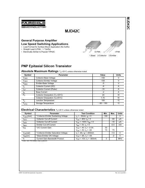
MJD42CMJD42CDISCLAIMERFAIRCHILD SEMICONDUCTOR RESERVES THE RIGHT TO MAKE CHANGES WITHOUT FURTHER NOTICE TO ANY PRODUCTS HEREIN TO IMPROVE RELIABILITY, FUNCTION OR DESIGN. FAIRCHILD DOES NOT ASSUME ANY LIABILITY ARISING OUT OF THE APPLICATION OR USE OF ANY PRODUCT OR CIRCUIT DESCRIBED HEREIN;NEITHER DOES IT CONVEY ANY LICENSE UNDER ITS PATENT RIGHTS, NOR THE RIGHTS OF OTHERS.LIFE SUPPORT POLICYFAIRCHILD’S PRODUCTS ARE NOT AUTHORIZED FOR USE AS CRITICAL COMPONENTS IN LIFE SUPPORT DEVICES OR SYSTEMS WITHOUT THE EXPRESS WRITTEN APPROVAL OF FAIRCHILD SEMICONDUCTOR CORPORATION.As used herein:TRADEMARKSThe following are registered and unregistered trademarks Fairchild Semiconductor owns or is authorized to use and is not intended to be an exhaustive list of all such trademarks.1. Life support devices or systems are devices or systems which, (a) are intended for surgical implant into the body,or (b) support or sustain life, or (c) whose failure to performwhen properly used in accordance with instructions for useprovided in the labeling, can be reasonably expected to result in significant injury to the user.2. A critical component is any component of a life support device or system whose failure to perform can bereasonably expected to cause the failure of the life support device or system, or to affect its safety or effectiveness.PRODUCT STATUS DEFINITIONS Definition of TermsDatasheet Identification Product Status DefinitionAdvance InformationFormative or In Design This datasheet contains the design specifications for product development. Specifications may change in any manner without notice.PreliminaryFirst ProductionThis datasheet contains preliminary data, andsupplementary data will be published at a later date.Fairchild Semiconductor reserves the right to make changes at any time without notice in order to improve design.No Identification Needed Full ProductionThis datasheet contains final specifications. Fairchild Semiconductor reserves the right to make changes at any time without notice in order to improve design.Obsolete Not In ProductionThis datasheet contains specifications on a product that has been discontinued by Fairchild semiconductor.The datasheet is printed for reference information only.A CEx™Bottomless™CoolFET™CROSSVOLT ™DenseTrench™DOME™EcoSPARK™E 2CMOS™EnSigna™FACT™FACT Quiet Series™FAST ®FASTr™FRFET™GlobalOptoisolator™GTO™HiSeC™ISOPLANAR™LittleFET™MicroFET™MICROWIRE™OPTOLOGIC™OPTOPLANAR™PACMAN™POP™Power247™PowerTrench ®QFET™QS™QT Optoelectronics™Quiet Series™SLIENT SWITCHER ®SMART START™STAR*POWER™Stealth™SuperSOT™-3SuperSOT™-6SuperSOT™-8SyncFET™TruTranslation™TinyLogic™UHC™UltraFET ®VCX™STAR*POWER is used under license。
SN74LS42D中文资料
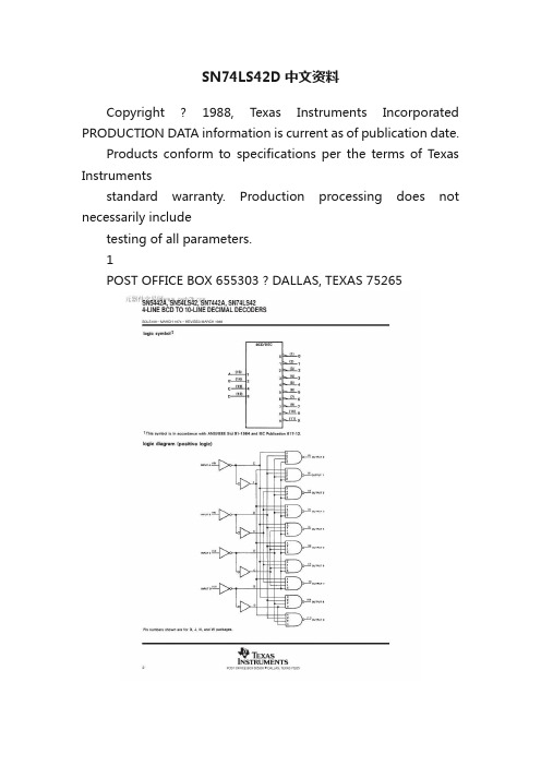
SN74LS42D中文资料Copyright ? 1988, Texas Instruments Incorporated PRODUCTION DATA information is current as of publication date.Products conform to specifications per the terms of Texas Instrumentsstandard warranty. Production processing does not necessarily includetesting of all parameters.1POST OFFICE BOX 655303 ? DALLAS, TEXAS 752652POST OFFICE BOX 655303 ? DALLAS, TEXAS 752653 POST OFFICE BOX 655303 ? DALLAS, TEXAS 752654POST OFFICE BOX 655303 ? DALLAS, TEXAS 752655 POST OFFICE BOX 655303 ? DALLAS, TEXAS 752656POST OFFICE BOX 655303 ? DALLAS, TEXAS 75265元器件交易网IMPORTANT NOTICETexas Instruments and its subsidiaries (TI) reserve the right to make changes to their products or to discontinueany product or service without notice, and advise customersto obtain the latest version of relevant informationto verify, before placing orders, that information being relied on is current and complete. All products are soldsubject to the terms and conditions of sale supplied at the time of order acknowledgement, including thosepertaining to warranty, patent infringement, and limitation of liability.TI warrants performance of its semiconductor products to the specifications applicable at the time of sale inaccordance with TI’s standard warranty. Testing and other quality control techniques are utilized to the extentTI deems necessary to support this warranty. Specific testing of all parameters of each device is not necessarilyperformed, except those mandated by government requirements.CERTAIN APPLICATIONS USING SEMICONDUCTOR PRODUCTS MAY INVOLVE POTENTIAL RISKS OFDEATH, PERSONAL INJURY, OR SEVERE PROPERTY OR ENVIRONMENTAL DAMAGE (“CRITICALAPPLICATIONS”). TI SEMICONDUCTOR PRODUCTS ARE NOT DESIGNED, AUTHORIZED, ORWARRANTED TO BE SUITABLE FOR USE IN LIFE-SUPPORT DEVICES OR SYSTEMS OR OTHERCRITICAL APPLICATIONS. INCLUSION OF TI PRODUCTS IN SUCH APPLICATIONS IS UNDERSTOOD TOBE FULLY AT THE CUSTOMER’S RISK.I n order to minimize risks associated with the customer’s applications, adequate design and operatingsafeguards must be provided by the customer to minimize inherent or procedural hazards.TI assumes no liability for applications assistance or customer product design. TI does not warrant or represent that any license, either express or implied, is granted under any patent right, copyright, mask work right, or other intellectual property right of TI covering or relating to any combination, machine, or process in which suchsemiconductor products or services might be or are used. TI’s publication of information regarding any thirdparty’s products or services does not constitute TI’s approval, warranty or endorsement thereof.Copyright ? 1999, Texas Instruments Incorporated。
PPD42NS 中文(日本神荣)
改订履历改订改订 日改 订 内 容确认 担当制定 2004.09.22 制定 臼井野間改订1 2007.04.01 公司名变更小山野間改订22009.02.20将发热电阻 RH1的导线掩盖,并在盒子上添加Rib。
藤本野間变更回路部件(Op Amp、volume、铝电解电容)。
型号改为PPD42NS。
1.适用范围本产品规格书适用于粉尘传感器单元PPD4NS PPD42NS (改订2)。
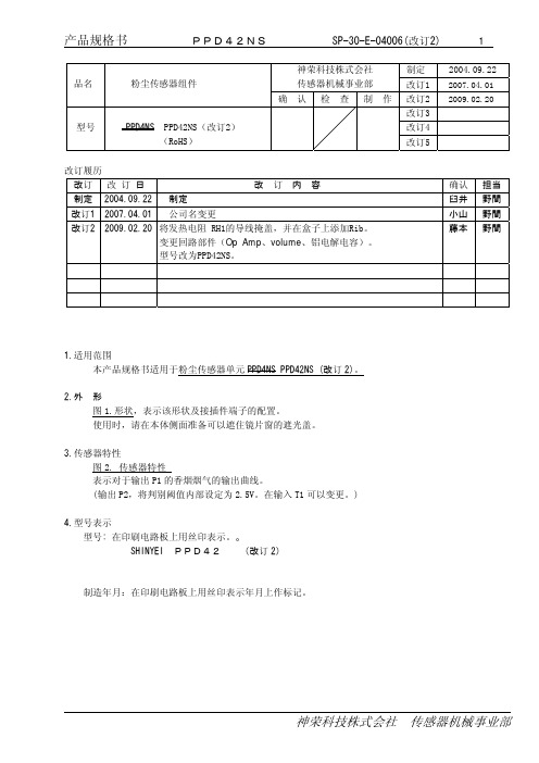
2.外 形图1.形状,表示该形状及接插件端子的配置。
使用时,请在本体侧面准备可以遮住镜片窗的遮光盖。
3.传感器特性图2. 传感器特性表示对于输出P1的香烟烟气的输出曲线。
(输出P2,将判别阈值内部设定为2.5V。
在输入T1可以变更。
)4.型号表示型号: 在印刷电路板上用丝印表示。
SHINYEI PPD42 (改订2)制造年月:在印刷电路板上用丝印表示年月上作标记。
编号 项 目内 容1 动作电源电压 DC 5V ±10% (CN1:Pin1=GND,Pin3=+5V)脉冲 30mV以下 2 消耗电流90mA3 动作温、湿度 0 ~ 45℃、95%rh 以下 (无结露)4 保存温度 -30 ~ 60℃5 尺 寸 W59 × H45 × D22(mm)6 质 量约 24g7 检知粒子直径 约 1μm以上8 检知浓度范围 清洁大气中,在约30m3的空间内,点燃约1根香烟(日本品牌:マイルドセブン(粒子计数器 在1μm以上范围中 約 8000個/283mL) 9 输出方式负论理 脉冲输出。
Lo 时间比率% (推荐单位时间 30秒)Hi:约4.5V 4V以上(改订2)、Lo:约 0.7V(输入阻抗为200kΩ时) OP AMP 输出 负载电阻10kΩ10 测定开始时间 电源启动后 约1分钟(电阻的温度稳定时间)6.依赖性试验 编号 试验项目 试验条件故障判定基准 供试数n 故障数C 无破损、裂缝。
CD42中文资料

Powerex, Inc., Hillis Street, Youngwood, Pennsylvania 15697 (724) 925-7272POW-R-BLOKTMDual SCR/Diode Isolated Module40 Amperes / Up to 1600 VoltsCD47__40ADescription:Powerex SCR/Diode Modules are designed for use in applications requiring phase control and isolated packaging. The modules are isolated for easy mounting with othercomponents on a common heatsink.POW-R-BLOK TMhas been tested and recognized by the Underwriters Laboratories.Features:T Electrically Isolated Heatsinking T DBC Alumina (Al 2O 3) Insulator T Copper BaseplateT Low Thermal Impedancefor Improved Current Capability T UL Recognized (E78240)Benefits:T No Additional Insulation Components Required T Easy Installation T No Clamping Components RequiredT Reduce Engineering TimeApplications:T Bridge Circuits T AC & DC Motor Drives T Battery Supplies T Power Supplies T Large IGBT Circuit Front Ends T Lighting Control T Heat & Temperature Control T WeldersPowerex, Inc., Hillis Street, Youngwood, Pennsylvania 15697 (724) 925-7272POW-R-BLOKTMDual SCR/Diode Isolated Module40 Amperes / Up to 1600 VoltsCD47__40AAbsolute Maximum RatingsCharacteristics Conditions Symbol UnitsRepetitive Peak Forward and Reverse Blocking VoltageV DRM & V RRMup to 1600 V Non-Repetitive Peak Reverse Blocking Voltage (t < 5 msec)V RSM V RRM + 100V RMS Forward Current 180° Conduction, T C =91°C 180° Conduction, T C =91°C (AC Switch)I T(RMS) I T(RMS) 63 93 A A Average Forward Current180° Conduction, T C =91°C I T(AV) 40 A Peak One Cycle Surge Current, Non-Repetitive60 Hz, 100% V RRM reapplied, T j =125°C 60 Hz, No V RRM reapplied, T j =125°C 60 Hz, No V RRM reapplied, T j =25°C50 Hz, 100% V RRMreapplied, T j=125°C50 Hz, No V RRM reapplied, T j =125°C 50 Hz, No V RRM reapplied, T j =25°CI TSM I TSM I TSM I TSM I TSM I TSM 750 890 985 715 850 940 A A A A A A Peak Three Cycle Surge Current, Non-Repetitive 60 Hz, 100% V RRM reapplied, T j =125°C50 Hz, 100% V RRM reapplied, T j =125°CI TSM I TSM 570 545 A A Peak Ten Cycle Surge Current, Non-Repetitive 60 Hz, 100% V RRM reapplied, T j =125°C 50 Hz, 100% V RRM reapplied, T j =125°C I TSM I TSM 460 445 A A I 2t for Fusing for One Cycle, 8.3 milliseconds8.3 ms, 100% V RRM reapplied, T j =125°C 8.3 ms, No V RRM reapplied, T j =125°C 8.3 ms, No V RRM reapplied, T j =25°C 10 ms, 100% V RRM reapplied, T j =125°C 10 ms, No V RRM reapplied, T j =125°C 10 ms, No V RRM reapplied, T j =25°CI 2t I 2t I 2t I 2t I 2t I 2t2,330 3,300 4,030 2,560 3,610 4,420A 2sec A 2 sec A 2 sec A 2 sec A 2 sec A 2 secMaximum Rate-of-Rise of On-State Current, (Non-Repetitive)T j =25°C, I G =0.5 A,V D =0.67 V DRM (Rated), I TM =300A ,T r < 0.5µs, t p > 6µsdi/dt 150 A/µsPeak Gate Power Dissipation T p < 5 ms, T j = 125°C P GM 10 W Average Gate Power Dissipation F = 50 Hz, T j = 125°C P G(AV) 2.5 W Peak Forward Gate Current T p < 5 ms, T j = 125°C I GFM 2.5 A Peak Reverse Gate Voltage T p < 5 ms, T j = 125°CV GRM 10 V Operating Temperature T J -40 to +125 °C Storage TemperatureT stg -40 to +125 °CMax. Mounting Torque, M5 Mounting Screw on Terminals25 3 in.-Lb.NmMax. Mounting Torque, Module to Heatsink 44 5 in.-Lb.NmModule Weight, Typical110 g3.88 oz.V Isolation @ 25CCircuit to base, all terminals shorted together50 – 60 Hz, 1 minute50 – 60 Hz, 1 secondV rms V rms2500 3500V VPowerex, Inc., Hillis Street, Youngwood, Pennsylvania 15697 (724) 925-7272POW-R-BLOKTMDual SCR/Diode Isolated Module40 Amperes / Up to 1600 VoltsCD47__40AElectrical Characteristics, T J =25°C unless otherwise specifiedCharacteristics Symbol Test Conditions Min. Max.UnitsRepetitive Peak Forward Leakage Current I DRM Up to 1600V, T J =125°C 15 mA Repetitive Peak Reverse Leakage Current I RRM Up to 1600V, T J =125°C 15 mAPeak On-State Voltage V TM / V FM I TM / I FM = 140A1.81 V Threshold Voltage, Low-level Slope Resistance, Low-level V (TO)1 r T1 T J = 125°C, I = 16.7% x πI T(AV) to πI T(AV)0.88 5.90V m ΩThreshold Voltage, High-level Slope Resistance, High-level V (TO)2 r T2 T J = 125°C, I = πI T(AV) to I TSM0.91 5.74 V m Ω V TM Coefficients, Full RangeT J = 125°C, I = 15% x I T(AV) to I TSMV TM = A+ B Ln I +C I + D Sqrt I A = B = C = D =0.872 -1.86 E-3 5.65 E-3 4.33 E-3Minimum dV/dt dV/dt Linear to 2/3 V DRMT j =125°C, Gate Open Circuit 500 V/µs Turn-Off Time (Typical)t offT J = 25°C, I T = 2 A V r = 50V, -dI/dt = 10 A/µs Re-Applied dV/dt = 200 V/µs,Linear to 900 V40 - 100 (Typical)µsGate Trigger Current I GT T j = -40°C, V D =6V, Resistive Load T j = 25°C, V D =6V, Resistive Load T j =125°C, V D =6V, Resistive Load 270 150 80 mAmA mA Gate Trigger Voltage V GT T j = -40°C, V D =6V, Resistive Load T j = 25°C, V D =6V, Resistive Load T j =125°C, V D =6V, Resistive Load4.0 2.5 1.7VoltsVolts VoltsNon-Triggering Gate Voltage V GDM T j =125°C, V D =V DRM 0.25 VoltsNon-Triggering Gate Current I GDM T j =125°C, V D =V DRM 6 mAHolding Current I H V D =6V, Resistive Load, Gate Open200 mA Latching CurrentI LV D =6V, Resistive Load400mAThermal CharacteristicsCharacteristics Symbol Max. Units Thermal Resistance, Junction to CaseDC OperationR ΘJ-C Per Module, both conducting Per Junction, both conducting0.230 0.460 °C/W°C/W Thermal Impedance CoefficientsZ ΘJ-CZ ΘJ-C = K 1 (1-exp(-t/τ1)) + K 2 (1-exp(-t/τ2)) + K 3 (1-exp(-t/τ3))+ K 4 (1-exp(-t/τ4)) K 1 = 1.77 E-2 K 2 = -1.00 E-2 K 3 = 1.46 E-1 K 4 = 3.07 E-1τ1 = 4.73 E-4τ2 = 1.67 E-3τ3 = 9.77 E-3τ4 = 8.76 E-2Thermal Resistance, Case to Sink LubricatedR ΘC-SPer Module0.1 °C/WPowerex, Inc., Hillis Street, Youngwood, Pennsylvania 15697 (724) 925-7272POW-R-BLOKTMDual SCR/Diode Isolated Module40 Amperes / Up to 1600 VoltsCD47__40AMaximum On-State Power Dissipation0510152025303540455055600510152025303540Average On-State Current - It/If(av) - AmperesM a x . P o w e r D i s s i p a t i o n P e r J u n c t i o n - W a t t s(Sinusoidal Waveform)Maximum On-State Power Dissipation010203040506070805101520253035404550556065Average On-State Current - It/If(av) - AmperesM a x . P o w e r D i s s i p a t i o n P e r J u n c t i o n - W a t t s(Rectangular Waveform)Maximum Allowable Case Temperature85909510010511011512012505101520253035404550556065Average On-State Current - It/If(av) - AmperesM a x . C a s e T e m p e r a t u r e - T c a s e -°C(Rectangular Waveform)Maximum Allowable Case Temperature9095100105110115120125510152025303540Average On-State Current - It/If(av) - AmperesM a x . C a s e T e m p e r a t u r e - T c a s e -°C(Sinusoidal Waveform)Maximum Transient Thermal Impedance0.000.050.100.150.200.250.300.350.400.450.500.0010.010.1110100Time - t - SecondsT h e r m a l I m p e d a n c e - R j c - °C /W(Junction to Case)Maximum On-State Forward Voltage Drop01234567101001000Instantaneous On-State Current - Itm/Ifm - AmperesO n -S t a t e V o l t a g e - V t m / V f m - V o l t s( Tj = 125 °C )。
EMS42GHD-14.7456M中文资料(ECLIPTEK)中文数据手册「EasyDatasheet - 矽搜」

MIL-STD-883,方法1010,条件B MIL-STD-883,方法1011,条件B MIL-STD-883,方法2007,条件A,20G
REEL
R
2.5分钟
M
1.5分钟
S
10分钟
N
O
P
Q
50分钟 20.2 MIN13.0 ±0.2 40分钟
T
U
V 数量/卷
18.4 MAX180 MAX 12.4 +2/-0 1,000
F
G HJ K
4.0 ±0.2 A0* 1.5 ±0.1/-0 B0* 0.30 ±0.05
EF
2.0 ±0.1
L
K0*
环境/机械特性
特有
ESD敏感性
可燃性 机械冲击 耐湿性 潮湿敏感度等级 耐焊接热 抗溶剂 可焊性
温度循环 热冲击 振荡
产品规格
MIL-STD-883,法3015,第2类,HBM:2000V UL94-V0 MIL-STD-883,方法2002,条件G,30,000G MIL-STD-883,法1004 J-STD-020, MSL 1 MIL-STD-202,方法210,满足条件K MIL-STD-202,方法215 MIL-STD-883,法2003(四个I / O焊盘
*Compliant to EIA 481C
标记规格
线路1:XXXX或XXXXX
EcliptekManufacturing Lot Code
ECLIPTEK CORP.
OSCILLATOR
EMS42
PLASTIC
2.5V
OS6R
.
04/10
规格如有更改,恕不另行通知.
PZTA42T1G;PZTA42T1;中文规格书,Datasheet资料

These Devices are Pb−Free, Halogen Free/BFR Free and are RoHS
MAXIMUM RATINGS (TC = 25C unless otherwise noted)
120 100 hFE , DC CURRENT GAIN 80 60 40 -55C 20 0 0.1 1.0 IC, COLLECTOR CURRENT (mA) 10 100 25C TJ = +125C VCE = 10 Vdc
Figure 1. DC Current Gain
Characteristics OFF CHARACTERISTICS Collector-Emitter Breakdown Voltage (Note 2) (IC = 1.0 mAdc, IB = 0) Collector-Base Breakdown Voltage (IC = 100 mAdc, IE = 0) Emitter-Base Breakdown Voltage (IE = 100 mAdc, IC = 0) Collector-Base Cutoff Current (VCB = 200 Vdc, IE = 0) Emitter-Base Cutoff Current (VBE = 6.0 Vdc, IC = 0) ON CHARACTERISTICS DC Current Gain (IC = 1.0 mAdc, VCE = 10 Vdc) (IC = 10 mAdc, VCE = 10 Vdc) (IC = 30 mAdc, VCE = 10 Vdc) DYNAMIC CHARACTERISTICS Current-Gain — Bandwidth Product (IC = 10 mAdc, VCE = 20 Vdc, f = 100 MHz) Feedback Capacitance (VCB = 20 Vdc, IE = 0, f = 1.0 MHz) Collector-Emitter Saturation Voltage (IC = 20 mAdc, IB = 2.0 mAdc) Base-Emitter Saturation Voltage (IC = 20 mAdc, IB = 2.0 mAdc) 2. Pulse Test Conditions, tp = 300 ms, d 0.02. fT Cre VCE(sat) VBE(sat) 50 − − − − 3.0 0.5 0.9 MHz pF Vdc Vdc hFE 25 40 40 − − − − V(BR)CEO V(BR)CBO V(BR)EBO ICBO IEBO 300 300 6.0 − − − − − 0.1 0.1 Vdc Vdc Vdc mAdc mAdc Symbol Min Max Unit
KSP2222A中文资料
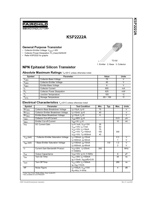
KSP2222ANPN Epitaxial Silicon TransistorAbsolute Maximum Ratings T a =25°C unless otherwise notedElectrical Characteristics T a =25°C unless otherwise noted* Pulse Test: Pulse Width ≤300µs, Duty Cycle ≤2%* Also available as and PN2222ASymbol ParameterValue Units V CBO Collector-Base Voltage 75V V CEO Collector-Emitter Voltage 40V V EBO Emitter-Base Voltage 6V I C Collector Current600mA P C Collector Power Dissipation 625mW T J Junction Temperature 150°C T STGStorage Temperature-55 ~ 150°CSymbol ParameterTest Condition Min.Typ.Max.Units BV CBO Collector-Base Breakdown Voltage I C =10µA, I E =075V BV CEO Collector Emitter Breakdown Voltage I C =10mA, I B =040V BV EBO Emitter-Base Breakdown Voltage I E =10µA, I C =06V I CBO Collector Cut-off Current V CB =60V, I E =00.01µA I EBO Emitter Cut-off Current V EB =3V, I C =010nAh FEDC Current GainI C =0.1mA, V CE =10V V CE =10V, I C =1mA V CE =10V, I C =10mA V CE =10V, *I C =150mA V CE =10V, *I C =500mA 35507510040300V CE (sat)* Collector-Emitter Saturation Voltage I C =150mA, I B =15mA I C =500mA, I B =50mA 0.31V V V BE (sat)* Base-Emitter Saturation Voltage I C =150mA, I B =15mA I C =500mA, I B =50mA 0.61.22V V f T Current Gain Bandwidth Product V CE =20V, I C =20mA f=100MHz300MHz C ob Output Capacitance V CB =10V, I E =0, f=1MHz 8pF t ON Turn On Time V CC =30V, I C =150mAI B1=15mA, V BE (off)=0.5V 35ns t OFF Turn Off Time V CC =30V, I C =150mA I B1=I B2=15mA 285ns NFNoise FigureI C =100µA, V CE =10V R S =IK Ω, f=1KHz4dBKSP2222AGeneral Purpose Transistor•Collector-Emitter Voltage: V CEO = 40V•Collector Power Dissipation: P C (max)=625mW •Refer KSP2222 for graphs1. Emitter2. Base3. CollectorTO-921KSP2222ADISCLAIMERFAIRCHILD SEMICONDUCTOR RESERVES THE RIGHT TO MAKE CHANGES WITHOUT FURTHER NOTICE TO ANY PRODUCTS HEREIN TO IMPROVE RELIABILITY, FUNCTION OR DESIGN. FAIRCHILD DOES NOT ASSUME ANY LIABILITY ARISING OUT OF THE APPLICATION OR USE OF ANY PRODUCT OR CIRCUIT DESCRIBED HEREIN;NEITHER DOES IT CONVEY ANY LICENSE UNDER ITS PATENT RIGHTS, NOR THE RIGHTS OF OTHERS.LIFE SUPPORT POLICYFAIRCHILD’S PRODUCTS ARE NOT AUTHORIZED FOR USE AS CRITICAL COMPONENTS IN LIFE SUPPORT DEVICES OR SYSTEMS WITHOUT THE EXPRESS WRITTEN APPROVAL OF FAIRCHILD SEMICONDUCTOR CORPORATION.As used herein:TRADEMARKSThe following are registered and unregistered trademarks Fairchild Semiconductor owns or is authorized to use and is not intended to be an exhaustive list of all such trademarks.1. Life support devices or systems are devices or systems which, (a) are intended for surgical implant into the body,or (b) support or sustain life, or (c) whose failure to performwhen properly used in accordance with instructions for useprovided in the labeling, can be reasonably expected to result in significant injury to the user.2. A critical component is any component of a life support device or system whose failure to perform can bereasonably expected to cause the failure of the life support device or system, or to affect its safety or effectiveness.PRODUCT STATUS DEFINITIONS Definition of TermsDatasheet Identification Product Status DefinitionAdvance InformationFormative or In Design This datasheet contains the design specifications for product development. Specifications may change in any manner without notice.PreliminaryFirst ProductionThis datasheet contains preliminary data, andsupplementary data will be published at a later date.Fairchild Semiconductor reserves the right to make changes at any time without notice in order to improve design.No Identification Needed Full ProductionThis datasheet contains final specifications. Fairchild Semiconductor reserves the right to make changes at any time without notice in order to improve design.Obsolete Not In ProductionThis datasheet contains specifications on a product that has been discontinued by Fairchild semiconductor.The datasheet is printed for reference information only.A CEx™Bottomless™CoolFET™CROSSVOLT ™DenseTrench™DOME™EcoSPARK™E 2CMOS™EnSigna™FACT™FACT Quiet Series™FAST ®FASTr™FRFET™GlobalOptoisolator™GTO™HiSeC™ISOPLANAR™LittleFET™MicroFET™MICROWIRE™OPTOLOGIC™OPTOPLANAR™PACMAN™POP™Power247™PowerTrench ®QFET™QS™QT Optoelectronics™Quiet Series™SLIENT SWITCHER ®SMART START™STAR*POWER™Stealth™SuperSOT™-3SuperSOT™-6SuperSOT™-8SyncFET™TruTranslation™TinyLogic™UHC™UltraFET ®VCX™STAR*POWER is used under license。
锡42铋58强度-概述说明以及解释
锡42铋58强度-概述说明以及解释1.引言1.1 概述概述部分的内容可以从以下几个方面进行展开:锡42铋58合金是一种由锡和铋组成的合金材料。
锡作为一种常见的金属材料,在工业领域有广泛的应用。
而铋则是一种稀有金属,拥有良好的导电性和热稳定性,以及抗腐蚀性能。
锡42铋58合金的组成比例为42的锡和58的铋,通过合金化可以获得具有特殊性能的材料。
锡42铋58合金具有一些独特的力学性能。
首先,该合金具有较高的强度和硬度,能够承受较大的拉伸力和压缩力。
其次,锡42铋58合金具有较好的延展性和韧性,在承受外力时能够发生一定的塑性变形而不容易断裂。
此外,该合金还具有良好的耐腐蚀性能,能够抵御氧化、腐蚀和各种化学介质的侵蚀。
锡42铋58合金的强度特点使其具有广泛的应用前景。
首先,在航空航天领域,该合金可以用于制造耐高温和耐蚀的发动机部件。
其次,在电子领域,锡42铋58合金可以作为导电材料用于制造高性能的导线和电子元件。
此外,在医疗器械和化工设备领域,该合金也可以用于制造具有抗腐蚀性和高强度要求的设备和部件。
综上所述,锡42铋58合金具有较高的强度和硬度,良好的延展性和韧性,以及优异的耐腐蚀性能,具有广泛的应用前景。
通过进一步研究和开发该合金的制备工艺和性能调控方法,有望进一步拓展该合金在各个领域的应用范围,并为相关行业的发展做出贡献。
1.2 文章结构文章结构部分的内容可以编写为:文章结构部分旨在介绍本文的章节安排和内容涵盖范围。
本文共分为引言、正文和结论三个部分。
引言部分主要包括概述、文章结构和目的三个小节。
在概述中,将简要介绍锡42铋58合金以及相关背景信息。
接下来,文章结构小节将详细说明文章各个部分的内容安排与主题。
最后,目的小节将明确本文探讨的目标和意义。
正文部分是本文的重点,主要涵盖了锡42铋58合金的组成和力学性能两个小节。
在锡42铋58合金的组成小节,将详细介绍该合金的化学成分和微结构。
同时,还会探讨合金中每个成分的作用及其对合金性能的影响。
PA42中文资料
l 1 概述PA42是美国APEX公司推出的一种高电压单片场效应管大功率运算放大器,它具有工作电压高(350V),静态电流小、输出电流大(峰值120mA,连续输出电流可达120mA)、价格低廉等特点。
使用该放大器可在提高可靠性的同时取得以前需在混合设计中才能达到的性能,它内部的输入保护电路避免了过高的共模、差模电压及静电泄放的影响,其安全工作区无二次击穿限制,因此只要选择合适的限流电阻就可驱动不同的负载。
通过PA42的外部可调补偿电路可以使设计人员根据具体的应用来选择合适的带宽和增益。
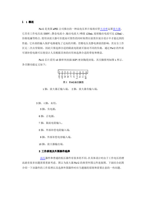
PA42芯片采用10脚单列直插(SIP)密封陶瓷封装,其引脚排列如图1所示。
各引脚功能定义如下:1脚:放大器正输入端; 2脚:放大器负输入端;3脚、4脚:未用;5脚:负电源;6脚:正电源;7脚:限流电阻输入;8脚:外部补偿电阻输入端;9脚:外部补偿电容输入端;10脚:放大器输出端。
2 工作原理及外围器件选择高压器件和普通的低压器件有很多的不同,在具体设计时由于工作电压的增高就有很多问题需要重新考虑,图2为放大器PA42的典型外围元件连接图。
下面结合此图介绍一下该器件的工作原理以及选择外围器件时应当遵循的原则和需要注意的一些问题。
2.1 限流及限流电阻为了使器件能够正常工作,图2中的限流电阻RcL的最小取值应为18Ω。
为了提高放大器的稳定性,在满足限流要求的前提下,应尽量选取较大阻值的限流电阻。
具体选取可根据下式来估计:RcL="3"/ILim应当说明:在实际计算器件总的输出电阻时,器件本身的典型输出电阻加上最终选取的限流电阻才是器件的实际输出电阻。
还有一点需要注意的是:通过全部负载电流和限流电阻可以得到输出电压幅度受实际限流电阻影响的具体值,其计算公式如下:VR="IoRcL"式中,VR为输出电压的减小量。
在实际设计中,对于对输出电压幅度有要求的场合,应选用一个合适的工作电源。
CA42中英文对照规格书全正文(新) FREE

修改记录Revision Record目录CATALOG1.适用范围Scope (3)2.产品代码说明 Product identification (3)3.规格范围 The range of the specification (3)4.电性参数检测标准、检测条件及其温度特性Temperature characteristic (4)5.形状及尺寸 Appearance & Dimensions (4)6.标志 Marking (5)7.容量范围、壳号The range of the capacitance and case (5)8.可靠性试验Reliable performance (6)9.无铅产品识别标识The lead-free product identifying label 710.特性曲线Typical Characteristic curve (7)11.包装Packing (9)12.安装方法 The method of mounting (12)13.使用注意事项Note in use (12)14.贮存 Storage (13)15.订货资料 Ordering information (13)1. 适用范围Scope本规格书适用于树脂包封固体电解质钽电容器(无铅)。
This specification applies to Epoxy-coated Solid Electrolytic Tantalum Capacitors (LEAD FREE ).2.产品代码说明 Product identification⑴ ⑵⑶ ⑷⑸ ⑹⑺说明Explain :⑴企业代码company logo ⑵产品型号series: CA42表示树脂包封固体电解质钽电容器的型号.CA42 representseries number of epoxy-coated solid electrolytic tantalum capacitors⑶容 量capacitance code :容量用皮法拉表示,前两位数字是有效数字,第三位数字是跟随零的个数。
KSP44中文资料
KSP44/45NPN Epitaxial Silicon TransistorAbsolute Maximum Ratings T a =25°C unless otherwise notedElectrical Characteristics T a =25°C unless otherwise noted* Pulse Test: PW ≤300µs, Duty Cycle ≤2%Symbol ParameterValue Units V CBO Collector-Base Voltage: KSP44 : KSP45500400V V V CEOCollector-Emitter Voltage: KSP44 : KSP45400350V V V EBO Emitter-Base Voltage 6V I C Collector Current300mA P C Collector Power Dissipation (T a =25°C)625mW P C Collector Power Dissipation (T C =25°C) 1.5W T JJunction Temperature150°CT STGStorage Temperature -55 ~ 150°CSymbol ParameterTest ConditionMin.Max.Units BV CBOCollector-Base Breakdown Voltage: KSP44: KSP45I C =100µA, I B =0500400V VBV CEO* Collector -Emitter Breakdown Voltage: KSP44: KSP45I C =1mA, I B =0400350V V BV EBO Emitter-Base Breakdown Voltage I E =100µA, I C =06VI CBOCollector Cut-off Current: KSP44: KSP45V CB =400V, I E =0V CB =320V, I E =00.10.1µA µA I CESCollector Cut-off Current: KSP44: KSP45V CE =400V, I B =0V CE =320V, I B =00.50.5µA µA I EBO Emitter Cut-off Current V EB =4V, I C =00.1µAh FE* DC Current GainV CE =10V, I C =1mA V CE =10V, I C =10mA V CE =10V, I C =50mA V CE =10V, I C =100mA 40504540200V CE (sat)* Collector-Emitter Saturation VoltageI C =1mA, I B =0.1mA I C =10mA, I B =1mA I C =50mA, I B =5mA 0.40.50.75V V V V BE (sat)* Base-Emitter Saturation Voltage I C =10mA, I B =1mA 0.75V C obOutput CapacitanceV CB =20V, I E =0, f=1MHz7pFKSP44/45High Voltage Transistor•Collector-Emitter Voltage: V CEO =KSP44: 400VKSP45: 350V•Collector Power Dissipation: P C (max)=625mW1. Emitter2. Base3. CollectorTO-921KSP44/45TRADEMARKSThe following are registered and unregistered trademarks Fairchild Semiconductor owns or is authorized to use and is not intended to be an exhaustive list of all such trademarks.DISCLAIMERFAIRCHILD SEMICONDUCTOR RESERVES THE RIGHT TO MAKE CHANGES WITHOUT FURTHER NOTICE TO ANY PRODUCTS HEREIN TO IMPROVE RELIABILITY, FUNCTION OR DESIGN. FAIRCHILD DOES NOT ASSUME ANY LIABILITY ARISING OUT OF THE APPLICATION OR USE OF ANY PRODUCT OR CIRCUIT DESCRIBED HEREIN;NEITHER DOES IT CONVEY ANY LICENSE UNDER ITS PATENT RIGHTS, NOR THE RIGHTS OF OTHERS.LIFE SUPPORT POLICYFAIRCHILD’S PRODUCTS ARE NOT AUTHORIZED FOR USE AS CRITICAL COMPONENTS IN LIFE SUPPORT DEVICES OR SYSTEMS WITHOUT THE EXPRESS WRITTEN APPROVAL OF FAIRCHILD SEMICONDUCTOR CORPORATION.As used herein:1. Life support devices or systems are devices or systems which, (a) are intended for surgical implant into the body,or (b) support or sustain life, or (c) whose failure to perform when properly used in accordance with instructions for use provided in the labeling, can be reasonably expected to result in significant injury to the user.2. A critical component is any component of a life support device or system whose failure to perform can be reasonably expected to cause the failure of the life support device or system, or to affect its safety or effectiveness.PRODUCT STATUS DEFINITIONS Definition of TermsDatasheet Identification Product Status DefinitionAdvance InformationFormative or In Design This datasheet contains the design specifications for product development. Specifications may change in any manner without notice.PreliminaryFirst ProductionThis datasheet contains preliminary data, andsupplementary data will be published at a later date.Fairchild Semiconductor reserves the right to make changes at any time without notice in order to improve design.No Identification Needed Full ProductionThis datasheet contains final specifications. Fairchild Semiconductor reserves the right to make changes at any time without notice in order to improve design.Obsolete Not In ProductionThis datasheet contains specifications on a product that has been discontinued by Fairchild semiconductor.The datasheet is printed for reference information only.FACT™FACT Quiet series™FAST ®FASTr™FRFET™GlobalOptoisolator™GTO™HiSeC™I 2C™ImpliedDisconnect™ISOPLANAR™LittleFET™MicroFET™MicroPak™MICROWIRE™MSX™MSXPro™OCX™OCXPro™OPTOLOGIC ®OPTOPLANAR™PACMAN™POP™Power247™PowerTrench ®QFET™QS™QT Optoelectronics™Quiet Series™RapidConfigure™RapidConnect™SILENT SWITCHER ®SMART START™SPM™Stealth™SuperSOT™-3SuperSOT™-6SuperSOT™-8SyncFET™TinyLogic™TruTranslation™UHC™UltraFET ®VCX™ACEx™ActiveArray™Bottomless™CoolFET™CROSSVOLT ™DOME™EcoSPARK™E 2CMOS™EnSigna™Across the board. Around the world.™The Power Franchise™Programmable Active Droop™。
CA42型插件钽电容器

H(max) 7.0 7.5 9.0 10 12 12.5
H(±0.5mm) 2.5 2.5 2.5 2.5 5.0 5.0
d(±0.5mm) 0.5 0.5 0.5 0.5 0.5 0.5
4、容量范围、壳号
容量(µF)
CODE
额定电压 (V)
4
6.3
10
16
25(20)
35
50
0.1
104
A
A
0.15
6.35±0.4 ±1.3max
CA42 类型
105 容量(μF)
标称容量(μF)
插件钽电 容器
前两位数字是有效数字
后一位数字是零的个数
M
035
A
容量精度 额定电压
脚距
K=±10% M=±20%
4V=004 6.3V=006 10V=010 16V=016
20v=020 25V=025 35V=035
Max D.F(%)
+20 +85 -55℃
℃℃
+125℃
Max DCL(µA)
+85 +125℃
℃
≤1.0
6
4
6
6
1.5~6.8 10~68
±10 ±15
8
6
8
8
±25
10 I0 12.5 I0
10 8 10
10
100~330
12 10 12
12
3、外形尺寸
壳号 A B C D E F
D(max) 4.4 5.0 5.5 6.0 7.2 8.5
CA42 型插件钽电容器
1、简介:
CA42 型插件钽电容器采用优质的防潮、阻燃性黄色环氧树脂粉末包封,激光打印,其具有 稳定性好、漏电流和介质损耗小、频率及温度特性好和寿命长等特性。适用于尖端军事、电 脑、汽车、通讯、高档家用电器等领域。本产品符合采用 EIC 384-3-1 标准制定的企业标准 QB/PWV-109-2003。
KSP42中文资料
KSP42/43NPN Epitaxial Silicon TransistorAbsolute Maximum Ratings T a =25°C unless otherwise notedElectrical Characteristics T a =25°C unless otherwise noted* Pulse Test: PW ≤300µs, Duty Cycle ≤2%Symbol ParameterValue Units V CBO Collector Base Voltage: KSP42 : KSP43300200V V V CEOCollector-Emitter Voltage: KSP42 : KSP43300200V V V EBO Emitter-Base Voltage 6V I C Collector Current500mA P C Collector Power Dissipation 625mW T J Junction Temperature 150°C T STGStorage Temperature-55 ~ 150°CSymbol ParameterTest ConditionMin.Max.Units BV CBOCollector-Base Breakdown Voltage: KSP42 : KSP43I C =100µA, I E =0300200V V BV CEO* Collector -Emitter Breakdown Voltage: KSP42 : KSP43I C =1mA, I B =0300200V V BV EBO Emitter-Base Breakdown Voltage I E =100µA, I C =06VI CBOCollector Cut-off Current: KSP42 : KSP43V CB =200V, I E =0V CB =160V, I E =0100100nA nAI EBOEmitter Cut-off Current: KSP42 : KSP43V BE =6V, I C =0V BE =4V, I C =0100100nA nAh FE* DC Current GainV CE =10V, I C =1mA V CE =10V, I C =10mA V CE =10V, I C =30mA 254040V CE (sat)* Collector-Emitter Saturation Voltage I C =20mA, I B =2mA 0.5V V BE (sat)* Base-Emitter Saturation Voltage I C =20mA, I B =2mA 0.9V C obOutput Capacitance: KSP42 : KSP43V CB =20V, I E =0f=1MHz34pF pF f TCurrent Gain Bandwidth ProductV CE =20V, I C =10mA f=100MHz50MHzKSP42/43High Voltage Transistor•Collector-Emitter Voltage: V CEO =KSP42: 300VKSP43: 200V•Collector Power Dissipation: P C (max)=625mW1. Emitter2. Base3. CollectorTO-921KSP42/43KSP42/43TRADEMARKSThe following are registered and unregistered trademarks Fairchild Semiconductor owns or is authorized to use and is not intended to be an exhaustive list of all such trademarks.DISCLAIMERFAIRCHILD SEMICONDUCTOR RESERVES THE RIGHT TO MAKE CHANGES WITHOUT FURTHER NOTICE TO ANY PRODUCTS HEREIN TO IMPROVE RELIABILITY, FUNCTION OR DESIGN. FAIRCHILD DOES NOT ASSUME ANY LIABILITY ARISING OUT OF THE APPLICATION OR USE OF ANY PRODUCT OR CIRCUIT DESCRIBED HEREIN;NEITHER DOES IT CONVEY ANY LICENSE UNDER ITS PATENT RIGHTS, NOR THE RIGHTS OF OTHERS.LIFE SUPPORT POLICYFAIRCHILD’S PRODUCTS ARE NOT AUTHORIZED FOR USE AS CRITICAL COMPONENTS IN LIFE SUPPORT DEVICES OR SYSTEMS WITHOUT THE EXPRESS WRITTEN APPROVAL OF FAIRCHILD SEMICONDUCTOR CORPORATION.As used herein:1. Life support devices or systems are devices or systems which, (a) are intended for surgical implant into the body,or (b) support or sustain life, or (c) whose failure to perform when properly used in accordance with instructions for use provided in the labeling, can be reasonably expected to result in significant injury to the user.2. A critical component is any component of a life support device or system whose failure to perform can be reasonably expected to cause the failure of the life support device or system, or to affect its safety or effectiveness.PRODUCT STATUS DEFINITIONS Definition of TermsDatasheet Identification Product Status DefinitionAdvance InformationFormative or In Design This datasheet contains the design specifications for product development. Specifications may change in any manner without notice.PreliminaryFirst ProductionThis datasheet contains preliminary data, andsupplementary data will be published at a later date.Fairchild Semiconductor reserves the right to make changes at any time without notice in order to improve design.No Identification Needed Full ProductionThis datasheet contains final specifications. Fairchild Semiconductor reserves the right to make changes at any time without notice in order to improve design.Obsolete Not In ProductionThis datasheet contains specifications on a product that has been discontinued by Fairchild semiconductor.The datasheet is printed for reference information only.FACT™FACT Quiet series™FAST ®FASTr™FRFET™GlobalOptoisolator™GTO™HiSeC™I 2C™ImpliedDisconnect™ISOPLANAR™LittleFET™MicroFET™MicroPak™MICROWIRE™MSX™MSXPro™OCX™OCXPro™OPTOLOGIC ®OPTOPLANAR™PACMAN™POP™Power247™PowerTrench ®QFET™QS™QT Optoelectronics™Quiet Series™RapidConfigure™RapidConnect™SILENT SWITCHER ®SMART START™SPM™Stealth™SuperSOT™-3SuperSOT™-6SuperSOT™-8SyncFET™TinyLogic™TruTranslation™UHC™UltraFET ®VCX™ACEx™ActiveArray™Bottomless™CoolFET™CROSSVOLT ™DOME™EcoSPARK™E 2CMOS™EnSigna™Across the board. Around the world.™The Power Franchise™Programmable Active Droop™。
钽电容资料

产品简介:CA 42型系列电容器是烧结阳极、树脂包封固体电解质钽电容器,产品采用优质的抗潮、阻燃性黄色环氧树脂粉末包封,激光打印标志,其性能符合并优于IEC384-15-3及IECQQC300201/US0003以及SJ/T10856-96技术规范,是为电视机、录像机、计算机、程控交换机、电话、仪器、仪表等军工和民用电子整机配套的理想产品。
主要技术性能:●使用温度范围: -55℃~+125℃ (大于85℃,以降额电压使用) ●额定电压: 见表I●漏电流: I 0≤0.02C R U R 或1uA(取大者)(20℃) ●损耗角正切tgδo (%):见表III●电容量范围: 0.047uF~680uF 见表I●电容量允许偏差: ±5%,±10%,±20%(特殊订购) ●壳型尺寸:见表II ●温度特性:见表III温度特性Temperature Characteristics表III table3容量变化 Capacitance Change 损耗最大值(%) DF Max. 漏电流最大值DCL Max. 容量Capacitance(uF) -55℃ +85℃ +125℃ -55℃ +20℃ +85℃ +125℃ +20℃ +85℃+125℃≤1.0 6 4 6 6 1.5~6.8 8 6 8 8 10~68 108 10 10100~680±10 ±15 ±2512101212I 0≤0.02C R U R或(or) (取大者whicheveris greater)10 I 012.5 I 0壳型尺寸一览表Dimensions-Milimeters表II table2壳号 Case SizeD(max) H(max) H(±0.5mm)d(±0.5mm)A 4.5 7.0 2.5 0.5B 5.0 8.0 2.5 0.5C 5.5 9.5 2.5 0.5D 6.5 11.0 2.5 0.5E 8.5 13.0 5.0 0.5 F9.516.55.00.5Brief Introduction:CA42 Series sinter-anode, epoxy-coated solid electrolyte tantalumcapacitorsareencapsulatedwithflame-retardantyellow epoxy powder, marked with laser. CA42 Series meets and exceeds the requirements of IEC Specification 384-15-3, IECQ Specification QC300201/US0003 and Technical Specification SJ/T10856-96, used in military and civil applications such as TV sets, camcorders, computers, Program-controlled electronic telephone switching systems, telephones, instruments and meters.Features:●Operating temperature Range:-55℃~+125℃;> 85℃ with rated voltage derating.●Rated Voltage: See table 1●DC leakage at 20℃: Please see Table 3 ●Capacitance range: 0.047uF~680uF, see table 1●Capacitance tolerance: ±20%,±10%,±5%,(for special order);●Case size and dimensions, Please see Table 2 ●Temperature characteristics: See Table 3引线形式 (允许有其它引线形式)Lead Styles (Other lead styles are available)包 装Packaging informationB: 袋装A: 弹匣式编带(符合IEC286-2标准)B: Bulk packA: Ammo pack( per Specification IEC286-2)容量范围、壳号Rated Voltage, Nominal Capacitance and Case Size表I table1-1额定电压(V) Rated Voltage 3 4 6.3 10 16 20 25 35 50 降额电压(V) Voltage Derating 2 2.5 4 6.3 10 13 16 2032 浪涌电压(V) Surge Voltage 45.281320 26334665标称电容量(uF)Capacitance壳号 Case Size0.047 AA 0.068 A A 0.1A A 0.15 AA 0.22 A A 0.33A A 0.47 A A 0.68A A 1.0 A A A AB 1.5 A A A AC 2.2A A A ABC 3.3 A A A B B BD 4.7 A A A A B B B C D 6.8 A A A B B C C DE 10 A A B B B C C D E 15 A A B C C D D EF 22 B B C C C D D E F 33 B B C D D E E F 47 C C D D D E E F 68 D D D D E F F 100 D D E E E F F 150 D E E E F 220 E E E F 330 E F F 470 F 680F特性曲线Typical Characteristic Curve损耗因素—频率曲线Dissipation factor vs frequency 频率 Frequency (Hz)名称 Designation 符号 Symbol 尺寸 Dimensions(mm)元件间距 Pitch of component P 12.7±1.0 给进孔间距 Feed hole pitch Po 12.7±0.3 基带宽度Tape widthW +1 18 -0.5 粘胶带宽度Hold down tape widthWo 12±0.5 给进孔位置Hole positionH3 +0.75 9 -0.5粘胶带位置Hold down tape positionW2 3.0max 元件顶部给进孔心距离Overall component alignmentH1 32.5max 元件偏差Component alignment △P ±1.3max 给进孔直径Feed hole diameterD 4.0±0.2 基带厚度Tape thickness T0.5±0.2 元件偏差Component alignment△h ±2.0max 引线切屑长度Length of snipped leads L 11max 引线脚切铆高度Lead clinch height H 16±0.5引线脚间距 Lead wire spacingS2.5±0.5 5.0±0.7给进孔中心至引线脚间距Feed hole center to wire center P1 5.10±0.53.85±0.7给进孔中心至元件中心间距Hole center to component center P2 6.35±0.4 元件引线根部到给进孔心距离 Component heightH2 +2 18 -0 引线直径 Lead diameterd0.5±0.05容量变化—频率曲线Capacitance change vs frequency频率 Frequency (Hz)容量变化—温度曲线Capacitance change with temperature温度 Temperature (℃)损耗因素0-1-2-3-4-5-6-7-8损耗因素D i s s i p a t i o n F a c t o r t g δ(%)容量变化C a p a c i t a n c e C h a n g e △C /C (%)86420-2-4-6-8容量变化C a p a c i t a n c e C h a n g e △C /C (%)-60-40-20.0 20 4080 100。
TWN4 MULTITECH NANO LEGIC 42 M 集成手册说明书
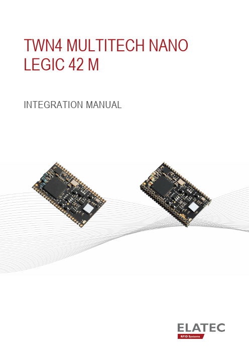
TWN4 MULTITECH NANO LEGIC 42 MINTEGRATION MANUALTABLE OF CONTENTS1INTRODUCTION (3)1.1ABOUT THIS MANUAL (3)1.2ABOUT TWN4 MULTITECH NANO LEGIC 42 M (3)1.3ELATEC SUPPORT (3)1.4REVISION HISTORY (3)2SAFETY INFORMATION (4)3INTEGRATION INSTRUCTIONS (5)3.1GENERAL (5)3.2LIST OF APPLICABLE RULES (5)3.3SPECIFIC OPERATIONAL USE CONDITIONS (5)3.4LIMITED MODULE PROCEDURES (5)3.5TRACE ANTENNA DESIGN (5)3.6RF EXPOSURE CONSIDERATIONS (4)3.7ANTENNAS (4)3.8LABEL AND COMPLIANCE INFORMATION (4)3.9TEST MODES AND ADDITIONAL TESTING REQUIREMENTS (4)3.10ADDITIONAL TESTING, PART 15 SUBPART B DISCLAIMER (5)3.11MECHANICAL INSTALLATION (5)3.12ELECTRICAL CONNECTION (5)3.13PROGRAMMATION/SOFTWARE INTEGRATION (5)4COMPLIANCE STATEMENTS (6)4.1EU (6)4.2FCC (6)4.3IC (6)4.4UNITED KINGDOM (6)5INTEGRATOR AND HOST REQUIREMENTS (7)APPENDIX (8)A – TERMS AND ABBREVIATIONS (8)B – RELEVANT DOCUMENTATION (8)1INTRODUCTION1.1ABOUT THIS MANUALThis integration manual explains how to integrate ELATEC RFID reader/writer module TWN4 MultiTech Nano LEGIC 42 M into a host device and is mainly intended for integrators and host manufacturers. Before installing the product, the integrators should read and understand the content of this integration manual and other relevant installation documents.The content of this integration manual is subject to changes without prior notice and printed versions might be obsolete. Integrators and host manufacturers are required to use the latest version of this integration manual.For the sake of better understanding and readability, this manual might contain exemplary pictures, drawings and other illustrations. Depending on your product configuration, these pictures might differ from the actual design of your product.The original version of this integration manual has been written in English. Wherever the integration manual is available in another language, it is considered as a translation of the original document for information purposes only. In case of discrepancy, the original version in English will prevail.1.2ABOUT TWN4 MULTITECH NANO LEGIC 42 MTWN4 MultiTech Nano LEGIC 42 M is designed for integration into machines or other devices. It can be connected to an external antenna through a printed circuit board (125 kHz, 13.56 MHz or both).1.3ELATEC SUPPORTIn case of any technical questions, refer to the ELATEC website () or contact ELATEC technical support at:***********************1.4REVISION HISTORYVERSION CHANGE DESCRIPTION EDITION01 First edition 04/20222SAFETY INFORMATION•ELATEC TWN4 MultiTech Nano LEGIC 42 M is an electronic component and should be installed exclusively by a trained and qualified personnel.•ELATEC recommends the integrators to follow general ESD protective measures during the installation of TWN4 MultiTech Nano LEGIC 42 M into a host device, e.g. the use of an antistatic wristband or special gloves.•The integrator should not touch the antennas (if not shielded), printed circuit boards, connectors or other sensitive components on TWN4 MultiTech Nano LEGIC 42 M.•Metallic materials on or in direct vicinity to the product might reduce the reading performance of the product. Refer to the installation instructions for more information.•Before installing TWN4 MultiTech Nano LEGIC 42 M into a host device, the integrator should also make sure that he/she has read and understood the ELATEC technical documentation related to TWN4 MultiTech Nano LEGIC 42 M, as well as the technical documentation related to the host device. In particular, the instructions and safety information given in the user manual of TWN4 MultiTech Nano LEGIC 42 M should be read carefully and listed in the technical documentation of the host manufacturer as well, as soon as these instructions and safety information are required for a safe and proper use of the host device containing TWN4 MultiTech Nano LEGIC 42 M.•Any failure to comply with the safety information given in this document and in the user manual, is considered improper use.ELATEC excludes any liability in case of improper use or faulty product installation.3INTEGRATION INSTRUCTIONS3.1GENERALTWN4 MultiTech Nano LEGIC 42 M may be installed in any host devices, as long as it is operated under the operational conditions stated in the user manual and other technical documents (e.g. data sheet).3.2LIST OF APPLICABLE RULESRefer to the approval certificates, grants and declarations of conformity issued for TWN4 MultiTech Nano LEGIC 42 M, and to Chapter “Compliance Statements” for a detailed list of the rules applicable to TWN4 MultiTech Nano LEGIC 42 M.•47 CFR 15.207 •47 CFR 15.209 •47 CFR 15.225 •RSS-Gen •RSS-102 •RSS-2103.3SPECIFIC OPERATIONAL USE CONDITIONSTWN4 MultiTech Nano LEGIC 42 M is an RFID reader module without antenna that can be connected to an external antenna through a printed circuit board (125 kHz, 13.56 MHz or both). TWN4 MultiTech Nano LEGIC 42 M has been tested with a printed circuit board equipped with specific antennas (refer to Chapter “Antennas” for detailed information). The use of TWN4 MultiTech Nano LEGIC 42 M with other antennas is technically possible. However, such use conditions require additional testing and/or approval.If TWN4 MultiTech Nano LEGIC 42 M is used with antennas as described under Chapter “Antennas”, there are no specific operational use conditions other than the conditions mentioned in the user manual and data sheet of TWN4 MultiTech Nano LEGIC 42 M. The host manufacturer or integrator must ensure that these use conditions comply with the use conditions of the host device. In addition, these use conditions must be stated in the user manual of the host device.3.4LIMITED MODULE PROCEDURESThe integrator must perform tests to ensure that all applicable rule parts are kept in combination with the end device (refer to Chapter “List of applicable rules”).3.5TRACE ANTENNA DESIGNFor antenna information, refer to Chapter “Antennas”.Tolerances Capacitors: 1% Resistors: 2%3.6RF EXPOSURE CONSIDERATIONSThe module antenna(s) must be installed to meet the RF exposure compliance separation distance of 0 cm and any additional testing and authorization process as required.Refer to Chapter “Compliance Statements” for detailed information about the radio frequency exposure conditions applicable to TWN4 MultiTech Nano LEGIC 42 M.These RF exposure conditions must be stated in the end-product manual(s) of the host product manufacturer.3.7ANTENNASTWN4 MultiTech Nano LEGIC 42 M has been tested with an external printed circuit board equipped with the following antennas:HF antenna on external PCB, printed, one-sided LF antenna on external PCB, glued and solderedHF antenna (13.56 MHz)Outer dimensions: 32 x 29.4 mm / 1.26 x 1.16 inchNumber of turns: 4Inductance: 1.0 µH ± 20%PCB trace width: 0.6 mm / 0.02 inchLF antenna (125 kHz)Outer diameter: max. 16.3 mm / 0.64 inchNumber of turns: 144Inductance: 490 µH ± 5%Wire diameter: 0.10 mm / 0.0039 inchLead free, coil fixed by using backed wirePlease note that the use of TWN4 MultiTech Nano LEGIC 42 M with other antennas than the ones described above is not part of the approvals granted to the module. In case TWN4 MultiTech Nano LEGIC 42 M is used with other antennas, a separate approval, additional testing or new authorization for a use with these specific antennas is required.For more information, refer to the related product data sheet or other relevant technical documents.3.8LABEL AND COMPLIANCE INFORMATIONRefer to Chapters “Compliance Statements” and “Integrator and Host Requirements” for detailed label and compliance information.3.9TEST MODES AND ADDITIONAL TESTING REQUIREMENTSNo specific testing method has been defined by ELATEC for TWN4 MultiTech Nano LEGIC 42 M.TWN4 MultiTech Nano LEGIC 42 M has been tested and found in compliance with the specifications noted on the approval certificates and other relevant approval documents. However, the integrator is still responsible for any additional testing and authorization process required for the end product.It is recommended that the host product manufacturer installing the modular transmitter perform some investigative measurements to confirm that the resulting composite system does not exceed the spurious emissions limits or band edge limits (e.g., where a different antenna may be causing additional emissions). Detailed information regarding test procedure are described in the relevant rule parts (refer to Chapter “List of applicable rules”).3.10ADDITIONAL TESTING, PART 15 SUBPART B DISCLAIMERTWN4 MultiTech Nano LEGIC 42 M is only FCC authorized for the specific rule parts (i.e., FCC transmitter rules) listed on the grant, and the host product manufacturer is responsible for compliance to any other FCC rules that apply to the host not covered by the modular transmitter grant of certification. In addition, the final host product still requires Part 15 Subpart B compliance testing with TWN4 MultiTech Nano LEGIC 42 M installed.3.11MECHANICAL INSTALLATIONTWN4 MultiTech Nano LEGIC 42 M is available in two different versions: C0 and C1Version C0 (SMT) Version C1 (THT)The version C0 is equipped with solder pads on both sides that enable to integrate (i.e. solder) the module directly onto the PCB or host device using the SMT technology, whereas the pin connectors on the version C1 are suitable for THT mounting.For both versions, the components are mounted only on one side of the module to allow an easy integration into the host device.3.12ELECTRICAL CONNECTION3.13PROGRAMMATION/SOFTWARE INTEGRATIONn/a4 COMPLIANCE STATEMENTS4.1 EUTWN4 MultiTech Nano LEGIC 42 M is in compliance with the EU directives and regulations as listed in the respective declaration of conformity.4.2 FCCThis device complies with Part 15 of the FCC Rules. Operation is subject to the following two conditions: (1) this device may not cause harmful interference, and (2) this device must accept any interference received, including interference that may cause undesired operation. Caution The Federal Communications Commission (FCC) warns the users that changes or modifications to the unit not expressly approved by the party responsible for compliance could void the user's authority to operate the equipment. FCC §15.105 (b) This equipment has been tested and found to comply with the limits for a Class B digital device, pursuant to part 15 of the FCC Rules. These limits are designed to provide reasonable protection against harmful interference in a residential installation. This equipment generates, uses and can radiate radio frequency energy and, if not installed and used in accordance with the instructions, may cause harmful interference to radio communications. However, there is no guarantee that interference will not occur in a particular installation. If this equipment does cause harmful interference to radio or television reception, which can be determined by turning the equipment off and on, the user is encouraged to try to correct the interference by one or more of the following measures:• Reorient or relocate the receiving antenna.• Increase the separation between the equipment and receiver.• Connect the equipment into an outlet on a circuit different from that to which the Receiver is connected.• Consult the dealer or an experienced radio/TV technician for help.FCC ID: WP5TWN4F204.3 ICThis device complies with Industry Canada’s license-exempt RSSs. Operation is subject to the following two conditions: (1) This device may not cause interference; and (2) This device must accept any interference, including interference that may cause undesired operation of the device. Le présent appareil est conforme aux CNR d’Industrie Canada applicables aux appareils radio exempts de licence. L’exploitation est autorisée aux deux conditions suivantes: (1) l’appareil ne doit pas produire de brouillage; (2) l’utilisateur de l’appareil doit accepter tout brouillage radioélectrique subi, même si le brouillage est susceptible d’en compromettre le fonctionnement.IC: 7948A-TWN4F204.4 UNITED KINGDOMTWN4 MultiTech Nano LEGIC 42 M complies with the requirements of the UK legislations and other regulations as listed in the respective UK declaration of conformity. The importer is responsible for applying the following information to the packaging of theproduct: • the importer company’s details, including the company’s name and a contact address in the UnitedKingdom.• UKCA marking5INTEGRATOR AND HOST REQUIREMENTS Authorization requirementsTWN4 MultiTech Nano LEGIC 42 M has been certified as a module and does not need further approval, provided that the module: •is used with antennas as specified in this manual; and•is used in accordance with the FCC grant conditions and no limitations or usage conditions have been defined by ELATEC. However, the host manufacturer must ensure that the host device still complies with all applicable regulations after TWN4 MultiTech Nano LEGIC 42 M has been integrated.In particular, the host integrator installing TWN4 MultiTech Nano LEGIC 42 M into their product must ensure that the final composite product complies with the FCC requirements by a technical assessment or evaluation to the FCC rules, including the transmitter operation and should refer to guidance in KDB 996369.Labeling requirementsThe FCC and IC identification numbers of TWN4 MultiTech Nano LEGIC 42 M can be found in Chapter “Compliance Statements” of the user manual and on the device packaging. After integration of TWN4 MultiTech Nano LEGIC 42 M into the host device, it is necessary to bring a label on the host device (on a visible and accessible place) stating the FCC and IC identification numbers of the integrated TWN4 MultiTech Nano LEGIC 42 M:Contains FCC ID: WP5TWN4F20Contains IC: 7948A-TWN4F20In case several modules have been integrated into the host device, the label should state all FCC and IC identification numbers of the integrated modules.Example:“Contains FCC IDs: XXX-XXXXXXX, YYY-YYYYYYY, ZZZ-ZZZZZZZ”“Contains transmitter modules IC: XXXXX-XXXXXX, YYYYY-YYYYYY, ZZZZZ-ZZZZZZ”Compliance statementsAll statements listed in Chapter “Compliance statements” of this integration manual must be also listed in the user manual of the host device.Special accessoriesWhere special accessories such as shielded cables and/or special connectors are required to comply with the emission limits, the instruction manual shall include appropriate instructions on the first page of the text describing the installation of the device.Simultaneous transmissionWhen the host product supports simultaneous-transmission operations the host manufacturer needs to check if there are additional RF exposure filing requirements due to the simultaneous transmissions. When additional application filing for RF exposure compliance demonstration is not required (e. g. the RF module in combination with all simultaneously operating transmitters complies with the RF exposure simultaneous transmission SAR test exclusion requirements), the host manufacturer may do his own evaluation without any filing, using reasonable engineering judgment and testing for confirming compliance with out-of-band, restricted band, and spurious emission requirements in the simultaneous-transmission operating modes. If additional filing is required please contact the person at ELATEC GmbH responsible for certification of the RF module.APPENDIXA – TERMS AND ABBREVIATIONSTERM EXPLANATIONhost device Also “host” or “host product”. Device in which an RFID module is intended to be installed for operation.Integrator Responsible party for the integration of an RFID module into a host device. The integrator might be the module manufacturer, the host manufacturer, the end user or any other third party.KDB Knowledge Databasemodular type Physical configuration in which a modular transmitter operates when installed within a host device. It can be a single-modular, a limited single-modular, a split-modular or a limited split-modular type.n/a Not applicableRFID (reader/writer) module Device intended to be used within another device or product. Depending on the equipment configuration and intended use, an RFID module has to meet different requirements to get a modular grant.SMT Surface Mount TechnologyTHT Through Hole TechnologyB – RELEVANT DOCUMENTATIONELATEC documentation•TWN4 MultiTech Nano LEGIC 42 M data sheet•TWN4 MultiTech Nano LEGIC 42 M functional description•TWN4 MultiTech Nano LEGIC 42 M user manual•TWN4 MultiTech Nano technical handbookExternal documentationDocument name Document title/description Sourcen/a Technical documentation related to thehost product Host product manufacturer784748 D01 General labeling and Notification General Guidelines for Labeling andOther Information Required to beProvided to UsersFederal Communications CommissionOffice of Engineering and TechnologyLaboratory Division996369 D01 Module Equip Auth Guide Transmitter Module EquipmentAuthorization Guide Federal Communications Commission Office of Engineering and Technology Laboratory Division996369 D02 Module Q and A Frequently Asked Questions andAnswers about Modules Federal Communications Commission Office of Engineering and Technology Laboratory Division996369 D03 OEM Manual Guidance for Modular TransmitterInstruction Manuals and TCBCertification Application ReviewsFederal Communications CommissionOffice of Engineering and TechnologyLaboratory Division996369 D04 Module Integration Guide Modular Transmitter Integration Guide—Guidance for Host ProductManufacturersFederal Communications CommissionOffice of Engineering and TechnologyLaboratory DivisionRSS-Gen General Requirements for Compliance ofRadio Apparatus Innovation, Science and Economic Development CanadaRSS-102 Radio Frequency (RF) ExposureCompliance of RadiocommunicationApparatus (All Frequency Bands)Innovation, Science and EconomicDevelopment CanadaFor more information about this integration manual or TWN4 MultiTech Nano LEGIC 42 M, go to or contact ELATEC.Elatec reserves the right to change any information or data in this document without prior notice. Elatec declines all responsibility for the use of this product with any other specification but the one mentioned above. Any additional requirement for a specific customer application has to be validated by the customer himself at his own responsibility. Where application information is given, it is only advisory and does not form part of the specification. Disclaimer: All names used in this document are registered trademarks of their respective owners.© 2022 ELATEC GmbH – TWN4 MultiTech Nano LEGIC 42 M integration manual DocRev1 – 04/2022ELATEC GMBHZeppelinstr. 1 • 82178 Puchheim • Germany P +49 89 552 9961 0 • F +49 89 552 9961 129 • E-mail:********************。
ksp——精选推荐

ksp溶度积表化合物化学式温度K sp来源⽆⽔氢氧化铝Al(OH)320°C 1.9×10⁻³³L⽆⽔氢氧化铝Al(OH)325°C 3×10–34w1三⽔合氢氧化Al(OH)320°C 4×10–13 C铝三⽔合氧化铝Al(OH)325°C 3.7×10⁻¹³ C 磷酸铝AlPO425°C 9.84×10⁻²¹w1溴酸钡Ba(BrO3)225°C 2.43×10⁻⁴w1碳酸钡BaCO316°C 7×10⁻⁹C, L 碳酸钡BaCO325°C 8.1×10⁻⁹C, L 铬酸钡BaCrO428°C 2.4×10⁻¹⁰C, L 氟化钡BaF225.8°C1.73×10–6C, L ⼆⽔合碘酸钡Ba(IO3)225°C 6.5×10⁻¹⁰C, L ⼆⽔合草酸钡BaC2O418°C 1.2×10⁻⁷C, L 硫酸钡BaSO418°C 0.87×10⁻¹⁰C, L 硫酸钡BaSO425°C 1.08×10⁻¹⁰C, L 硫酸钡BaSO450°C 1.98×10⁻¹⁰C, L 氢氧化铍Be(OH)225°C 6.92×10⁻²²w1碳酸镉CdCO325°C 1.0×10⁻¹²w1氢氧化镉Cd(OH)225°C 7.2×10⁻¹⁵w1三⽔合草酸镉CdC2O418°C 1.53×10⁻⁸C, L 磷酸镉Cd3(PO4)2 25°C2.53×10–33w1硫化镉CdS 18°C3.6×10–29C, L碳酸钙(⽅解CaCO315°C 0.99×10⁻⁸C, L ⽯)碳酸钙(⽅解CaCO325°C 0.87×10⁻⁸C, L ⽯)碳酸钙(⽅解CaCO318-25°C 4.8×10⁻⁹P ⽯)铬酸钙CaCrO418°C 2.3×10⁻²L氟化钙CaF218°C 3.4×10⁻¹¹C, L 氟化钙CaF225°C 3.95×10⁻¹¹C, L 氢氧化钙Ca(OH)218°C-25°C 8×10⁻⁶P氢氧化钙Ca(OH)225°C 5.02×10⁻⁶w1六⽔合碘酸钙Ca(IO3)218°C 6.44×10⁻⁷L⼀⽔合草酸钙CaC2O4 18°C 1.78×10⁻⁹C, L ⼀⽔合草酸钙CaC2O4 25°C 2.57×10⁻⁹C, L 磷酸钙Ca3(PO4)225°C 2.07×10⁻³³w1硫酸钙CaSO410°C 6.1×10⁻⁵C, L 硫酸钙CaSO425°C 4.93×10⁻⁵w1⼆⽔合酒⽯酸CaC4H4O618°C 7.7×10⁻⁷C, L 钙氢氧化亚铬Cr(OH)225°C 2×10–16w2氢氧化铬Cr(OH)325°C 6.3×10⁻³¹w2氢氧化钴Co(OH)225°C 1.6×10⁻¹⁵w2硫化钴CoS 18°C 3×10–26C, L 硫化钴CoS 18°C-25°C 10–21P碳酸铜CuCO325°C 1×10⁻¹⁰P氢氧化铜Cu(OH)218°C-25°C 6×10–20P氢氧化铜Cu(OH)225°C 4.8×10⁻²⁰w1碘酸铜Cu(IO3)225°C 1.4×10⁻⁷C, L 草酸铜CuC2O425°C 2.87×10⁻⁸C, L 硫化铜CuS 18°C 8.5×10–45C, L 溴化亚铜CuBr 18°C-20°C 4.15×10⁻⁸ C氯化亚铜CuCl 18°C-20°C 1.02×10⁻⁶ C氢氧化亚铜Cu(OH) 25°C 2×10–15w1(与氧化亚铜平衡)碘化亚铜CuI 18°C-20°C 5.06×10⁻¹² C硫化亚铜Cu2S 16°C-18°C 2×10–47C, L 硫氰化亚铜CuSCN 18°C 1.64×10⁻¹¹C, L 氢氧化铁Fe(OH)318°C 1.1×10–36C, L 碳酸亚铁FeCO318°C-25°C 2×10–11P氢氧化亚铁Fe(OH)218°C 1.64×10⁻¹⁴C, L 氢氧化亚铁Fe(OH)225°C 1×10–15; 8.0×10⁻¹⁶P; w2草酸亚铁FeC2O425°C 2.1×10⁻⁷C, L 硫化亚铁FeS 18°C 3.7×10⁻¹⁹C, L溴化铅PbBr225°C 6.3×10⁻⁶; 6.60×10⁻⁶ P; w1碳酸铅PbCO318°C 3.3×10⁻¹⁴C, L 铬酸铅PbCrO418°C 1.77×10⁻¹⁴C, L 氯化铅PbCl225.2°C 1.0×10⁻⁴L氯化铅PbCl218°C-25°C 1.7×10⁻⁵P氟化铅PbF218°C 3.2×10⁻⁸C, L 氟化铅PbF226.6°C 3.7×10⁻⁸C, L 氢氧化铅Pb(OH)225°C 1×10–16; 1.43×10⁻²⁰P; w1碘酸铅Pb(IO3)218°C 1.2×10⁻¹³C, L 碘酸铅Pb(IO3)225.8°C 2.6×10⁻¹³C, L 碘化铅PbI215°C 7.47×10⁻⁹ C碘化铅PbI225°C 1.39×10⁻⁸ C草酸铅PbC2O418°C 2.74×10⁻¹¹C, L 硫酸铅PbSO418°C 1.6×10⁻⁸C, L 硫化铅PbS 18°C 3.4×10⁻²⁸C, L 碳酸锂Li2CO325°C 1.7×10⁻³C, L 氟化锂LiF 25°C 1.84×10⁻³w1磷酸锂Li3PO425° 2.37×10⁻⁴w1磷酸铵镁MgNH4PO425°C 2.5×10⁻¹³C, L 碳酸镁MgCO312°C 2.6×10⁻⁵C, L 氟化镁MgF218°C 7.1×10⁻⁹C, L 氟化镁MgF225°C 6.4×10⁻⁹C, L 氢氧化镁Mg(OH)218°C 1.2×10⁻¹¹C, L 草酸镁MgC2O4 18°C 8.57×10⁻⁵C, L 碳酸锰MnCO318°C-25°C 9×10–11P氢氧化锰Mn(OH)218°C 4×10–14C, L 硫化锰(粉⾊)MnS 18°C 1.4×10⁻¹⁵C, L 硫化锰(绿⾊)MnS 25°C 10–22P溴化汞HgBr225°C 8×10–20L氯化汞HgCl225°C 2.6×10⁻¹⁵L氢氧化汞Hg(OH)225°C 3.6×10⁻²⁶w1(与氧化汞平衡)碘化汞HgI225°C 3.2×10⁻²⁹L硫化汞HgS 18°C 4×10–53 to 2×10–49C, L 溴化亚汞HgBr 25°C 1.3×10⁻²¹C, L 氯化亚汞Hg2Cl225°C 2×10–18C, L 碘化亚汞HgI 25°C 1.2×10⁻²⁸C, L 硫酸亚汞Hg2SO425°C 6×10⁻⁷; 6.5×10⁻⁷P; w1氢氧化镍Ni(OH)225°C 5.48×10⁻¹⁶w1硫化镍NiS 18°C 1.4×10⁻²⁴C, L 硫化镍NiS 18°C-25°C 10–27P硫化镍NiS 18°C-25°C 10–21P酒⽯酸钾KHC4H4O618°C 3.8×10⁻⁴C, L ⾼氯酸钾KClO425°C 1.05×10⁻²w1⾼碘酸钾KIO425° 3.71×10⁻⁴w1⼄酸银AgC2H3O216°C 1.82×10⁻³L溴酸银AgBrO320°C 3.97×10⁻⁵C, L 溴酸银AgBrO325°C 5.77×10⁻⁵C, L 溴化银AgBr 18°C 4.1×10⁻¹³C, L 溴化银AgBr 25°C 7.7×10⁻¹³C, L 碳酸银Ag2CO325°C 6.15×10⁻¹²C, L 氯化银AgCl 4.7°C 0.21×10⁻¹⁰C, L 氯化银AgCl 9.7°C0.37×10–10L氯化银AgCl 25°C 1.56×10⁻¹⁰C, L 氯化银AgCl 50°C 13.2×10⁻¹⁰C, L 氯化银AgCl 100°C 21.5×10⁻¹⁰C, L 铬酸银Ag2CrO414.8°C 1.2×10⁻¹²C, L 铬酸银Ag2CrO425°C 9×10–12C, L 氰化银Ag2(CN)220°C 2.2×10⁻¹²C, L 重铬酸银Ag2Cr2O725°C 2×10⁻⁷L氢氧化银AgOH 20°C 1.52×10⁻⁸C, L 碘酸银AgIO39.4°C 0.92×10⁻⁸C, L 碘化银AgI 13°C 0.32×10⁻¹⁶C, L 碘化银AgI 25°C 1.5×10⁻¹⁶C, L 亚硝酸银AgNO225°C 5.86×10⁻⁴L草酸银Ag2C2O425°C 1.3×10⁻¹¹L硫酸银Ag2SO418°C-25°C 1.2×10⁻⁵P硫化银Ag2S 18°C 1.6×10–49C, L 硫氰化银AgSCN 18°C 0.49×10⁻¹²C, L 硫氰化银AgSCN 25°C 1.16×10⁻¹²C, L 碳酸锶SrCO325°C 1.6×10⁻⁹C, L 铬酸锶SrCrO418°C-25°C 3.6×10⁻⁵P氟化锶SrF218°C 2.8×10⁻⁹C, L 草酸锶SrC2O418°C 5.61×10⁻⁸C, L 硫酸锶SrSO4 2.9°C 2.77×10⁻⁷C, L 硫酸锶SrSO417.4°C 2.81×10⁻⁷C, L 溴化铊TlBr 25°C 4×10⁻⁶L氯化铊TlCl 25°C 2.65×10⁻⁴L硫酸铊Tl2SO425°C 3.6×10⁻⁴L硫氰化铊TlSCN 25°C; 2.25×10⁻⁴L氢氧化锡Sn(OH)218°C-25°C 1×10–26P氢氧化锡Sn(OH)225°C 5.45×10⁻²⁷;1.4×10⁻²⁸w1;w2硫化锡SnS 25°C 10–28P氢氧化锌Zn(OH)218°C-20°C 1.8×10⁻¹⁴C, L ⼆⽔合草酸锌ZnC2O418°C 1.35×10⁻⁹C, L 硫化锌ZnS 18°C 1.2×10⁻²³C, L 参考资料:L=Lange's 10th ed.; C=CRC 44th ed.; P=General Chemistry by Pauling, 1970 ed.; w1=⽹络来源1; w2=⽹络来源2。
TA42DU-42-20热电流保护器说明书

Degree of Protection
Pollution Degree Connecting Capacity Auxiliary Circuit
2
2CDC106002M5701
1SAZ300401F0001
54 mm 90 mm 111 mm
Technical
Setting Range Rated Operational Voltage
Rated Operational Current (Ie) Rated Operational Current AC-3 (Ie) Rated Frequency (f)
Rated Impulse Withstand Voltage (Uimp ) Rated Insulation Voltage (Ui) Number of Poles Number of Auxiliary Contacts NC Number of Auxiliary Contacts NO Number of Protected Poles Conventional Free-air Thermal Current (Ith) Rated Operational Current AC-15 (Ie)
Connecting Capacity Main Circuit UL/CSA Connecting Capacity Auxiliary Circuit UL/CSA Tightening Torque UL/CSA
Main Circuit 600 V AC
42 A (NC:) B600 (NO:) C300 Flexible 1/2x 8-1 AWG Stranded 1/2x 8-1 AWG Flexible 1/2x 18-14 AWG Stranded 1/2x 18-14 AWG Auxiliary Circuit 12 in·lb Main Circuit 40 in·lb
- 1、下载文档前请自行甄别文档内容的完整性,平台不提供额外的编辑、内容补充、找答案等附加服务。
- 2、"仅部分预览"的文档,不可在线预览部分如存在完整性等问题,可反馈申请退款(可完整预览的文档不适用该条件!)。
- 3、如文档侵犯您的权益,请联系客服反馈,我们会尽快为您处理(人工客服工作时间:9:00-18:30)。
KSP42/43NPN Epitaxial Silicon TransistorAbsolute Maximum Ratings T a =25°C unless otherwise notedElectrical Characteristics T a =25°C unless otherwise noted* Pulse Test: PW ≤300µs, Duty Cycle ≤2%Symbol ParameterValue Units V CBO Collector Base Voltage: KSP42 : KSP43300200V V V CEOCollector-Emitter Voltage: KSP42 : KSP43300200V V V EBO Emitter-Base Voltage 6V I C Collector Current500mA P C Collector Power Dissipation 625mW T J Junction Temperature 150°C T STGStorage Temperature-55 ~ 150°CSymbol ParameterTest ConditionMin.Max.Units BV CBOCollector-Base Breakdown Voltage: KSP42 : KSP43I C =100µA, I E =0300200V V BV CEO* Collector -Emitter Breakdown Voltage: KSP42 : KSP43I C =1mA, I B =0300200V V BV EBO Emitter-Base Breakdown Voltage I E =100µA, I C =06VI CBOCollector Cut-off Current: KSP42 : KSP43V CB =200V, I E =0V CB =160V, I E =0100100nA nAI EBOEmitter Cut-off Current: KSP42 : KSP43V BE =6V, I C =0V BE =4V, I C =0100100nA nAh FE* DC Current GainV CE =10V, I C =1mA V CE =10V, I C =10mA V CE =10V, I C =30mA 254040V CE (sat)* Collector-Emitter Saturation Voltage I C =20mA, I B =2mA 0.5V V BE (sat)* Base-Emitter Saturation Voltage I C =20mA, I B =2mA 0.9V C obOutput Capacitance: KSP42 : KSP43V CB =20V, I E =0f=1MHz34pF pF f TCurrent Gain Bandwidth ProductV CE =20V, I C =10mA f=100MHz50MHzKSP42/43High Voltage Transistor•Collector-Emitter Voltage: V CEO =KSP42: 300VKSP43: 200V•Collector Power Dissipation: P C (max)=625mW1. Emitter2. Base3. CollectorTO-921KSP42/43KSP42/43TRADEMARKSThe following are registered and unregistered trademarks Fairchild Semiconductor owns or is authorized to use and is not intended to be an exhaustive list of all such trademarks.DISCLAIMERFAIRCHILD SEMICONDUCTOR RESERVES THE RIGHT TO MAKE CHANGES WITHOUT FURTHER NOTICE TO ANY PRODUCTS HEREIN TO IMPROVE RELIABILITY, FUNCTION OR DESIGN. FAIRCHILD DOES NOT ASSUME ANY LIABILITY ARISING OUT OF THE APPLICATION OR USE OF ANY PRODUCT OR CIRCUIT DESCRIBED HEREIN;NEITHER DOES IT CONVEY ANY LICENSE UNDER ITS PATENT RIGHTS, NOR THE RIGHTS OF OTHERS.LIFE SUPPORT POLICYFAIRCHILD’S PRODUCTS ARE NOT AUTHORIZED FOR USE AS CRITICAL COMPONENTS IN LIFE SUPPORT DEVICES OR SYSTEMS WITHOUT THE EXPRESS WRITTEN APPROVAL OF FAIRCHILD SEMICONDUCTOR CORPORATION.As used herein:1. Life support devices or systems are devices or systems which, (a) are intended for surgical implant into the body,or (b) support or sustain life, or (c) whose failure to perform when properly used in accordance with instructions for use provided in the labeling, can be reasonably expected to result in significant injury to the user.2. A critical component is any component of a life support device or system whose failure to perform can be reasonably expected to cause the failure of the life support device or system, or to affect its safety or effectiveness.PRODUCT STATUS DEFINITIONS Definition of TermsDatasheet Identification Product Status DefinitionAdvance InformationFormative or In Design This datasheet contains the design specifications for product development. Specifications may change in any manner without notice.PreliminaryFirst ProductionThis datasheet contains preliminary data, andsupplementary data will be published at a later date.Fairchild Semiconductor reserves the right to make changes at any time without notice in order to improve design.No Identification Needed Full ProductionThis datasheet contains final specifications. Fairchild Semiconductor reserves the right to make changes at any time without notice in order to improve design.Obsolete Not In ProductionThis datasheet contains specifications on a product that has been discontinued by Fairchild semiconductor.The datasheet is printed for reference information only.FACT™FACT Quiet series™FAST ®FASTr™FRFET™GlobalOptoisolator™GTO™HiSeC™I 2C™ImpliedDisconnect™ISOPLANAR™LittleFET™MicroFET™MicroPak™MICROWIRE™MSX™MSXPro™OCX™OCXPro™OPTOLOGIC ®OPTOPLANAR™PACMAN™POP™Power247™PowerTrench ®QFET™QS™QT Optoelectronics™Quiet Series™RapidConfigure™RapidConnect™SILENT SWITCHER ®SMART START™SPM™Stealth™SuperSOT™-3SuperSOT™-6SuperSOT™-8SyncFET™TinyLogic™TruTranslation™UHC™UltraFET ®VCX™ACEx™ActiveArray™Bottomless™CoolFET™CROSSVOLT ™DOME™EcoSPARK™E 2CMOS™EnSigna™Across the board. Around the world.™The Power Franchise™Programmable Active Droop™。
