Open103V-Schematic
LT8637 42V, 5A Synchronous Step-Down Silent Switch

1Rev. 0DESCRIPTIONLT863742V, 5A Synchronous Step-Down Silent Switcherwith 2.5μA Quiescent CurrentDemonstration circuit 3020A is a 42V, 5A (7A Peak) syn-chronous step-down Silent Switcher ® with spread spec-trum frequency modulation featuring the L T ®8637. The demo board is designed for 5V output from a 5.8V to 42V input. The wide input range allows a variety of input sources, such as automotive batteries and industrial sup-plies. The LT8637 is a compact, low emission, high effi-ciency, and high frequency synchronous monolithic step-down switching regulator . The LT8637 is the same as the LT8636, except it has a VC pin for external compensation. This allows the customer to optimize the loop response, or to parallel multiple regulators for higher current appli-cations. The proprietary Silent Switcher architecture mini-mizes electromagnetic emissions with simplified filter and reduced layout sensitivity. Selectable spread spectrum mode further improves EMI performance, making it per-fect solution to the noise sensitive applications. The regu-lator’s ultralow 2.5μA quiescent current–with the output in full regulation–enables applications requiring highest efficiency at very light load currents, such as automotive and battery powered portable instruments.Peak current mode control with minimum on-time of as small as 30ns allows high step-down conversion even at high frequency. The LT8637 switching frequency can be programmed either via oscillator resistor or external clockAll registered trademarks and trademarks are the property of their respective owners.PERFORMANCE SUMMARYover a 200kHz to 3MHz range. The default frequency of demo circuit 3020A is 2MHz.The SYNC/MODE pin on the demo board DC3020A is grounded (JP1 at BURST position) by default for low ripple Burst Mode ® operation. To synchronize to an external clock, move the Jump JP1 to SYNC/FCM and apply the external clock to the SYNC terminal ON THE 3020A. In sync mode, the part runs in forced continuous mode. Without external clock applied, the SYNC/MODE pin is floating, and the part runs in forced continuous mode. This mode offers fast transient response and full frequency operation over a wide load range. Alternatively, move the Jump JP1 to the SPREAD-SPECTRUM, and the SYNC/MODE is tied to INTVCC, the part runs in forced continuous mode with spread spectrum function enabled. The LT8637 data sheet gives a complete description of the part, operation and application information. The data sheet must be read in conjunction with this demo manual for demo circuit 3020A. The layout recommendations for low EMI operation and best thermal performance are available in the data sheet section Low EMI PCB Layout and Thermal Considerations and Peak Output Current. Contact ADI applications engineer for support.Design files for this circuit board are available .Specifications are at T A = 25°CSYMBOL PARAMETERCONDITIONSMIN TYPMAX UNITSV IN_EMI Input Supply Range with EMI Filter 5.842V V OUT Output Voltage4.855 5.15V I OUT Maximum Output Current Derating is Necessary for Certain V IN and Thermal Conditions 5Af SW Switching Frequency 1.852 2.15MHz EFFEfficiencyV IN = 12V, I OUT = 3A94.4%QUICK START PROCEDUREDemonstration circuit 3020A is easy to set up to evalu-ate the performance of the LT8637. Refer to Figure 1 for proper measurement equipment setup and follow the procedure below:NOTE: When measuring the input or output voltage ripple, care must be taken to avoid a long ground lead on the oscilloscope probe. Measure the output voltage ripple by touching the probe tip directly across the output capacitor.1. Make sure the Jump JP1 is on the BURST position. Refer to the schematic.2. With power off, connect the DC power supply to VEMI and GND. Connect the load from VOUT to GND.3. Connect the voltage meter across the VIN_SENSE and GND for V IN measurement, and VOUT_SENSE and GND for V OUT measurement.4. Turn on the power at the input.NOTE: Make sure that the input voltage does not exceed 42V.5. Check for the proper output voltage (V OUT = 5V). NOTE: If there is no output, temporarily disconnect theload to make sure that the load is not set too high or is shorted.6. Once the proper output voltage is established, adjust the load within the operating ranges and observe the output voltage regulation, ripple voltage, efficiency and other parameters. For efficiency measurement, use the VIN_SENSE, GND, and VOUT_SENSE, GND accordingly.7. An external clock can be added to the SYNC terminal when SYNC function is used (JP1 on the SYNC position). When JP1 is in SYNC, and no external clock is connected to the SYNC terminal of the board, the SYNC/FCM pin is floating, and the LT8637 runs in forced continuous mode. JP1 can also set LT8637 in spread spectrum mode (JP1 on the SPREAD-SPECTRUM position).Figure 1. Proper Measurement Equipment Setup2Rev. 0QUICK START PROCEDUREEfficiency, 12V IN, FCMFigure 2. Efficiency vs Load Current, 12V IN, V OUT = 5VCISPR25 Radiated Emission Test with Class 5 Average LimitsFigure 3. Radiated Emission Test with CISPR 25, Average Limit, SS Mode. V IN = 14V, I OUT = 5A, V OUT = 5V3Rev. 0PARTS LISTITEM QTY REFERENCE PART DESCRIPTION MANUFACTURER/PART NUMBERRequired Circuit Components11C1CAP., 22µF, ALUM. ELECT., 63V, 20%, 6.3mm × 7.7mm, CE-BS SUN ELECTRONIC INDUSTRIES CORP, 63CE22BS 23C2, C10, C11CAP., 10µF, X7R, 50V, 10%, 1210, NO SUBS. ALLOWED MURATA, GRM32ER71H106KA12L32C3, C4CAP., 1µF, X5R, 50V, 10%, 0603AVX, 06035D105KAT2A41C5CAP., 0.1µF, X7R, 16V, 10%, 0603WURTH ELEKTRONIK, 885012206046 51C6CAP., 10pF, X7R, 50V, 10%, 0603AVX, 06035C100KAT2A61C7CAP., 100µF, X5R, 6.3V, 10%, 1206MURATA, GRM31CR60J107KE39L72C8, C16CAP., 1µF, X7R, 10V, 10%, 0603AVX, 0603ZC105KAT2A83C12, C13, C15CAP., 0.1µF, X7R, 50V, 10%, 0402AVX, 04025C104KAT2A91C17CAP., 560pF, C0G, 50V, 5%, 0603AVX, 06035A561JAT2A101C18CAP., 68pF, C0G, 50V, 5%, 0603AVX, 06035A680JAT2A111FB1IND., 30Ω AT 100MHz, FERRITE BEAD, 25%, 5A, 10mΩ, 0603TDK, MPZ1608S300ATAH0121L1IND., 2.2µH, 20%, 18.1A, 6.70mΩ, 6.56mm × 6.36mm,COILCRAFT, XEL6060-222MEBXEL6060, AEC-Q200131L2IND., 0.33µH, 20%, 19.2A, 3.52mΩCOILCRAFT, XAL5030-331MEB142R1, R4RES., 100k, 1%, 1/10W, 0603, AEC-Q200VISHAY, CRCW0603100KFKEA151R2RES., 17.8k, 1%, 1/10W, 0603, AEC-Q200NIC, NRC06F1782TRF161R3RES., 243k, 1%, 1/10W, 0603VISHAY, CRCW0603243KFKEA171R6RES., 1M, 1%, 1/10W, 0603, AEC-Q200VISHAY, CRCW06031M00FKEA181R7RES., 0Ω, 1/10W, 0603, AEC-Q200VISHAY, CRCW06030000Z0EA191R9RES., 8.06k, 1%, 1/10W, 0603YAGEO, RC0603FR-078K06L201U1IC, SYN. STEP-DOWN Silent Switcher, LQFN-20, 42V, 5A/7A ANALOG DEVICES, LT8637EV#PBF Additional Demo Board Circuit Components10R8RES., OPTION, 0603Hardware: For Demo Board Only14E2, E9, E11, E12TEST POINT, TURRET, 0.064" MTG. HOLE, PCB 0.062" THK MILL-MAX, 2308-2-00-80-00-00-07-0 26E4-E8, E10TEST POINT, TURRET, 0.094" MTG. HOLE, PCB 0.062" THK MILL-MAX, 2501-2-00-80-00-00-07-0KEYSTONE, 575-4 34J1-J4CONN., BANANA JACK, FEMALE, THT, NON-INSULATED,SWAGE, 0.218"41JP1CONN., HDR., MALE, 2 × 3, 2mm, VERT, STR, THT WURTH ELEKTRONIK, 6200062112154MH1-MH4STANDOFF, NYLON, SNAP-ON, 0.50"WURTH ELEKTRONIK, 70293500061XJP1CONN., SHUNT, FEMALE, 2-POS, 2mm SAMTEC, 2SN-BK-G4Rev. 05Rev. 0Information furnished by Analog Devices is believed to be accurate and reliable. However , no responsibility is assumed by Analog Devices for its use, nor for any infringements of patents or other rights of third parties that may result from its use. Specifications subject to change without notice. No license is granted by implication or otherwise under any patent or patent rights of Analog Devices.SCHEMATIC DIAGRAMP h o n e : (4086Rev. 0ANALOG DEVICES, INC. 202103/21ESD CautionESD (electrostatic discharge) sensitive device. Charged devices and circuit boards can discharge without detection. Although this product features patented or proprietary protection circuitry, damage may occur on devices subjected to high energy ESD. Therefore, proper ESD precautions should be taken to avoid performance degradation or loss of functionality.Legal Terms and ConditionsBy using the evaluation board discussed herein (together with any tools, components documentation or support materials, the “Evaluation Board”), you are agreeing to be bound by the terms and conditions set forth below (“Agreement”) unless you have purchased the Evaluation Board, in which case the Analog Devices Standard Terms and Conditions of Sale shall govern. Do not use the Evaluation Board until you have read and agreed to the Agreement. Your use of the Evaluation Board shall signify your acceptance of the Agreement. This Agreement is made by and between you (“Customer”) and Analog Devices, Inc. (“ADI”), with its principal place of business at One Technology Way, Norwood, MA 02062, USA. Subject to the terms and conditions of the Agreement, ADI hereby grants to Customer a free, limited, personal, temporary, non-exclusive, non-sublicensable, non-transferable license to use the Evaluation Board FOR EVALUATION PURPOSES ONL Y. Customer understands and agrees that the Evaluation Board is provided for the sole and exclusive purpose referenced above, and agrees not to use the Evaluation Board for any other purpose. Furthermore, the license granted is expressly made subject to the following additional limitations: Customer shall not (i) rent, lease, display, sell, transfer , assign, sublicense, or distribute the Evaluation Board; and (ii) permit any Third Party to access the Evaluation Board. As used herein, the term “Third Party” includes any entity other than ADI, Customer , their employees, affiliates and in-house consultants. The Evaluation Board is NOT sold to Customer; all rights not expressly granted herein, including ownership of the Evaluation Board, are reserved by ADI. CONFIDENTIALITY. This Agreement and the Evaluation Board shall all be considered the confidential and proprietary information of ADI. Customer may not disclose or transfer any portion of the Evaluation Board to any other party for any reason. Upon discontinuation of use of the Evaluation Board or termination of this Agreement, Customer agrees to promptly return the Evaluation Board to ADI. ADDITIONAL RESTRICTIONS. Customer may not disassemble, decompile or reverse engineer chips on the Evaluation Board. Customer shall inform ADI of any occurred damages or any modifications or alterations it makes to the Evaluation Board, including but not limited to soldering or any other activity that affects the material content of the Evaluation Board. Modifications to the Evaluation Board must comply with applicable law, including but not limited to the RoHS Directive. TERMINATION. ADI may terminate this Agreement at any time upon giving written notice to Customer . Customer agrees to return to ADI the Evaluation Board at that time. LIMITATION OF LIABILITY. THE EVALUATION BOARD PROVIDED HEREUNDER IS PROVIDED “AS IS” AND ADI MAKES NO WARRANTIES OR REPRESENTATIONS OF ANY KIND WITH RESPECT TO IT . ADI SPECIFICALL Y DISCLAIMS ANY REPRESENTATIONS, ENDORSEMENTS, GUARANTEES, OR WARRANTIES, EXPRESS OR IMPLIED, RELATED TO THE EVALUATION BOARD INCLUDING, BUT NOT LIMITED TO, THE IMPLIED WARRANTY OF MERCHANTABILITY, TITLE, FITNESS FOR A PARTICULAR PURPOSE OR NONINFRINGEMENT OF INTELLECTUAL PROPERTY RIGHTS. IN NO EVENT WILL ADI AND ITS LICENSORS BE LIABLE FOR ANY INCIDENTAL, SPECIAL, INDIRECT , OR CONSEQUENTIAL DAMAGES RESUL TING FROM CUSTOMER’S POSSESSION OR USE OF THE EVALUATION BOARD, INCLUDING BUT NOT LIMITED TO LOST PROFITS, DELAY COSTS, LABOR COSTS OR LOSS OF GOODWILL. ADI’S TOTAL LIABILITY FROM ANY AND ALL CAUSES SHALL BE LIMITED TO THE AMOUNT OF ONE HUNDRED US DOLLARS ($100.00). EXPORT . Customer agrees that it will not directly or indirectly export the Evaluation Board to another country, and that it will comply with all applicable United States federal laws and regulations relating to exports. GOVERNING LAW . This Agreement shall be governed by and construed in accordance with the substantive laws of the Commonwealth of Massachusetts (excluding conflict of law rules). Any legal action regarding this Agreement will be heard in the state or federal courts having jurisdiction in Suffolk County, Massachusetts, and Customer hereby submits to the personal jurisdiction and venue of such courts. The United Nations Convention on Contracts for the International Sale of Goods shall not apply to this Agreement and is expressly disclaimed.。
工厂专业术语
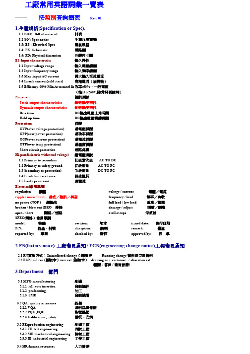
Rev: 011.生產規格(Specification or Spec).1.1 BOM: Bill of material 料表 1.2 S/N: Spec notice 生產注意事項 1.3: ES : Electrical Spec 電氣規格 1.4: PK: Schematic 電路圖 1.5: PD: Physical dimension 外觀尺寸圖ES:Input characterstics 輸入特性 1.1 Input voltage range 輸入電壓範圍 1.2 Input frequency range 輸入頻率範圍 1.3 Max .input AC current 最大輸入交流電流 1.4 Inrush current(cold start)突增電流突增電流((冷開機冷開機)) 1.5 Efficency:60% Min.At nomarl line 效率效率:60%,一般電壓(指115/230V,除非另有說明除非另有說明))Noise test 雜訊測試 Static output characteristics 靜態輸出特性 Dynamic output characteristics 動態輸出特性 Rise time DC 輸出電壓上升時間 Hold up time DC 輸出電壓持續時間Protection:保護 OVP(over voltage protection)過電壓保護 OPP(over power protection)過功率保護 OCP(over current protection)過電流保護 OTP(over temp protection)過溫度保護 Short circuit protection 短路保護Hi-pot(dielectric withstand voltage)耐電壓測試 1.1 Primary to secondary 初級對次級 AC TO DC 1.2 Primary to safety ground 初級對地 AC TO FG 1.3 Secondary to protection)次級對地 DC TO FG 1.4 Insulation resistance 絕緣阻抗 1.5 Leakage current 漏電流Electrical 常用單詞regulation 調整voltage / current 電壓電壓電壓//電流ripple / noise / buzz 漣波漣波//雜訊雜訊//異音frequency / load 頻率頻率//負載no power (NOP ) ) 無輸出無輸出full load / low load 重載重載//輕載broken / blow out (BRO 燒機damage / adjust 損壞損壞//調整open / short 開路開路開路//短路oscilloscope 示波器SPEC(規格規格))常用單詞model: 機種revision: 版本issued date: 發行日期P/N: 品名品名,,料號discrption: 說明remark: 備注reported by: 草擬cheched by: 審核approved by: 核 準2.FN(factory noice):工廠變更通知 / ECN(engineering change notice)工程變更通知2.1 FN 實施方式實施方式:: Immediated change 立即變更 Running change 舊料用完用新料 2.2 ECN: old rev.(舊版本舊版本))new rev.(新版本新版本)) drawing no / customer / alteration ref (圖號 / 客戶 / 變更依據)3.Department 部門3.1 MFG:manufacturing 制造3.1.1 AI: auto insertion 自動插件 3.1.2 preforming 加工3.1.3 SMD自動粘著 3.2 QA: quality assurance 品保3.2.1 VQA進料品質保證 3.2.2 PQC ,FQC製程品管 3.2.3 Calibration , safety 儀校儀校,,安規 3.3 PE:production engineering 制造工程 3.3.1 TE:test engineering測試工程 3.3.2 ME:mechanical engineering 機械工程 3.3.3 IE: industrial engineering 工業工程 3.4 HR:human resources人力資源工廠常用英語詞彙一覽表按類別查詢簡表3.5 Material物料3.5.1 PC:production control生管3.5.2 purchasing采購3.5.3 warehouse倉庫3.6 ENG:engineering工程3.6.1 document center資料中心4. Safety4.1 UL(Underwriters Laboratories)美國保險協會實驗室4.2 CSA(Canadian Standards Association)加拿大標準協會4.3 TUV德國技術監護協會4.4 VDE德國電氣標準4.5 NEMKO挪威電氣標準4.6 DEMKO丹麥電氣標準4.7 CCEE(China Commission for Conformity 中國電工產品認證委員會Certification of Electronial Equipment)4.8 CCIB(China Commodity Inspection Bureau)中國商品檢驗局5. Other 其他 FAX(傳真): date,to,fm,subject,dear,TKS,best regards,FAR: issue,description,corrective action,preventive action, analysis,defect,failure,supplier/vendor ISO:Internation Organization for Standardization 國際標準化組織Quality Manual:品質手冊Procedure: 作業程序Quality policy: Quality Reliability Excellence品質至上信賴第一追求卓越6.Contraction(縮寫)AQL: accept quality lecer 允收水準ATS: auto test system自動測試系統CR: critical嚴重ESD: electrostatic discharge靜電放電FET: field effective transistor場效電晶體ICT: in-circuit test線路測試MA: major主要MI:minor次要MRB: material review board不良材料審核組NTC: negative temperatire characteristic熱敏電阻O/I: operation instruction工作指導書PWM: pulse width modification脈波寬調整S/N: series number序號SMD: surface mounting device表面沾著WIP:work in progress半成品(工作進行中)JIT: just in timeIR: infra-red 紅外線的PDPC: process,decision,program,chartQCCA: quality control circle activities品管圈活動CWQC: company-wide quality control全面品管QCCA: quality control circle activities品管圈活動CWQC: company-wide quality control全面品管ponent(零件)bobbin線軸shield背板bridge diode橋式整流triode三極管cable tie束帶tape 膠布capactitor(cap)電容screw tapping自攻螺絲case外殼screw machine機械螺絲ceramic capacitor陶瓷電容terminal端子chip capacitor晶片電容transformer(X'FMR)變壓器chip resistor晶片電阻transistor電晶體choke線圈tube套管connector連接器varistor突波吸收器control board基板VR(variable resistance)可變電阻diode二極體washer 墊片epoxy樹脂zener齊納fan風扇photo couple光藕合二極體FET場效電晶體regulator穩壓器filter濾波器resistor電阻fuse保險絲ricer鉚釘fuse clip保險絲底座screw螺絲fuse holder保險絲底座socket插座glue膠solder bar錫棒heatsink散熱片sping washer彈簧墊片IC集成電路stand-off支柱inductor電感star washer星形墊片insulator絕緣片switch開關jumper wire跳線output cable輸出線label標簽output wire輸出線lock washer接地唾形墊片PCB電路板NTC熱敏電阻LED發光二極體nut螺絲帽tubber foot腳墊TEFLON鐵弗龍套管8.Time(時間)Jan.(January)一月month月份Feb.(February)二月period期間Mar.(March)三月quarter季Apr.(April)四月since從…..May五月week周Jun.(June)六月after 在……之後Jul.(July)七月before在……之前Aug.(August)八月date日期Sept.(September)九月Mon=Monday 星期一Oct.(October)十月Tue=Tuesday 星期二Nov.(November)十一月Wed=Wednesday 星期三Dec.(December)十二月Thu=Thuresday 星期四Fri=Friday 星期五Sat=Saturday 星期六Sun=Sunday 星期日9.Ver(動詞)change改變pay付給check檢查produce產生come來provide提供damage損傷receive收到find發現replace代替fix修理send發出go去take拿,采取happen發生touch踫觸improve改善wind纏(盤,卷)繞,扭曲insert插入issue發行make 做,使10.Non(名詞)action動作,措施analysis分析condition條件data資料defect缺點disposition處置engineer工程師failure失敗file文件夾inspector檢驗員11.Process(製程)assembly組立method方法burn-in(B/I)崩應model機種component零件noise噪音flux助焊劑pallet棧板function test功能測試paper紙張gravity比重plan設劃Hi-pot test耐高壓測試position位置insertion插件problem問題ORT可靠度測試procedure程序packing包裝product產品solder machine錫爐production生產station站別record記錄supplier/vendor廠商remark備注temperature溫度report報告humidity濕度requirement要求torque扭距sample樣品touch-up(T/U)補焊(二次作業)target目標layout設計圖trace(基板)線路location位置waybill運貨單manager經理operator作業員technician技術員12.Color(顏色)black黑色blue藍色brown棕色gold金色gray灰色green綠色orange橙色red紅色silver銀色violet(purple)紫色white白色yellow黃色13.Number(數字)二十one 一twenty 二十two 二twenty-one 二十一three 三thirty 三十四十four 四forty 四十五十five 五fifty 五十六十six 六sixty 六十seven 七seventy 七十eight 八seventy-three 七十三nine 九eighty 八十ten 十ninety 九十十一hundred 百eleven 十一十二thousand 千twelve 十二thirteen 十三million 萬十四fourteen 十四十五fifteen 十五十六sixteen 十六seventeen 十七eighteen 十八nineteen 十九14.基本單位換算長度:1m=10dm=10*10cm=10*10*10mm1inch=25.4mm面積:1立方米=10*10平方分米=104平方釐米=106=1.5-e3体積:1立方米=10+e3=10+e6=10+e9=10+e3=10+e6=264.2重量:1公斤=1千克=103克(g)1磅=453.59克(g)電氣:電感(L) 1亨(H)=103毫亨=106微亨電阻(R) 1千歐=103歐=106毫歐電容(C) 1法=106微法=1012皮法電壓(V) 1千伏=103伏=106毫伏電流(A) 1安=103毫安=106微安頻率(f) 1(MHz)=103千赫(KHz)=106赫茲(Hz)Page:210 of 215常用英文對照表(焊錫品質)極性反polarity reversed漏件missing part錯件wrong part壞件component無線尾no lead protruded裝插不良improper insertion零件偏移component shifted絕緣不良insulation damaged成型不良poor preforming錫洞solder void錫多excessive solder近似短路near short錫裂solder crack錫渣solder spatter錫橋solder bridge冷焊cold solder錫尖solder icicle短路solder short錫少solder in sufficient漏焊missing solder翹皮peeling off漏標示missing marking線腳長lead protrusion out of spec漏點膠missing glue防焊漆膠落solder mask peeling off污損contaminationPage:213 of 215常用英文對照表生產規格specification or spec光藕合二極體photo couple生產注意事項S/N突破吸收器varistor料表BOM(bill of material)場效電晶體pet電氣規格ES接地星形墊片lock washer電路圖PK橋片整流bridge diode外觀尺寸圖PD可變電阻VR(variable)零件符號圖PM晶片電阻chip resistor連片圖H-PCB陶瓷電容ceramic capacitance銅箔面布線圖PI保險絲座Fuse holder調整regulation熱敏電阻NTC機種model積體電路IC版本revision彈簧墊片spring washer發行日期issue date星形墊片star washer品名料號p/n二極體diode(dio)說明description電晶體transistor草擬reported by小基板control board審核checked by穩壓器regulator核準approved by電路板PCB生產通知FN(factory notice)濾波器filter工程變更通知ECN(engineering change notice)連接器connector立即變更immediately change輸出線output cable自然切換running change散熱片heat sink舊版本old rev絕緣片insulator新版本new rev電阻resistor(res)圖號drawing no電容capacitor客戶customer線圈choke倉庫warehouse電感inductor人力資源HR human resources齊納zener資料中心document control風扇fan追求卓越excellence外殼case品質至上quality開關switch信賴第一reliability插座socket零件component螺帽nut電氣electrical墊片washer制程process罩框housing線軸bobbin端子terminal束帶cable卯釘rivet螺絲screw套管tube塑膠柱space supportlr標簽label顏色color樹脂epoxy黑色black跳線jumper wirePage:214 of 215藍色blue錫棒solder bar棕色brown膠glue金色gold加工成型pre-forming灰色gray助焊劑flux綠色green插件insertion橙色orange錫燼solder machine紅色red比重gravity銀色silver溫度temperature紫色violet補焊touch-up白色white崩應burn-in黃色yellow組立assemby粉紅色pink包裝packing樣品sample測試test目標target調整adjust踫觸touch報表report方法method接地grounding處置disposition記錄record追蹤follow up產品product分析analysis變更change檢驗inspection修訂revise規格specification or spec重工rework缺點defect儲存storage修復repair更新update篩選sorting增加ADD備注remark刪除cancel正確地correct問題problem進料檢驗IQC治具fixture成品檢驗FQC安全safety流程圖flow chart計劃plan過電壓保護over voltage protection日期date過電流保護over current protection位置location過功率保護over power protection頻率frequency輸出output負載load漣波ripple滿載full load雜訊noise損壞damage異音noise buzz示波器oscillograph保護protection高壓測試hi-pot test燒機broken品質手冊quality manual電壓voltage品質政策quality policy電流current工作指導書operation instructor注意專心attention允收accept風扇不轉fan no turn功能function研究中under study材料materionPage:215 of 215報警器警戒使警覺alarm參考refer to請求request退貨reject不同different變更依據alteration ref錯誤過失error作業程序procedure百萬分之一 1 ppm極性反polarity reversed最大負載max load漏件missing part電腦computer錯件wrong part控制control壞件component標志marking無線尾no lead protruded制程品質保證PQA裝插不良improper insertion漏電流leakage currem零件偏移component shifted錫solder絕緣不良insulation damaged範圍range成型不良poor preforming棧板pallet錫洞solder void開關電源供應器switch power supply錫多excessive solder高壓hi-pot近似短路near short作業員operator錫裂solder crack主要major錫渣solder spatter檢查check錫橋solder bridge批lot冷焊cold solder加嚴tightened錫尖solder icicle安全安規safety短路solder short額定的rated錫少solder in sufficient電壓下降drop漏焊missing solder正常標準的normal翹皮peeling off顯示器display漏標示missing marking碟裝tray線腳長lead protrusion out of spec蓋子lid漏點膠missing glue塑膠袋pi bat防焊漆膠落solder mask peeling off紙板pad污損contamination干燥劑dryer當機shut down保護膜pi film誤判NDT隔板partition重調re-adjust單箱carton測試板test board海棉pu foam外殼下蓋lower case保力龍EPS外殼上蓋upper case遙控的remote保險絲fuse判斷不公(錯誤)misjudge選擇開關select switch主席chairman核對check。
x9c103s 用法 -回复

x9c103s 用法-回复题目:x9c103s 用法详解与示范(1500-2000字)引言:x9c103s是一个数字电位器芯片,是一种用于模拟电路调节的可变电阻器。
它具有调节电阻值、节省空间、易于控制等优点,在电子设备的设计和制造中广泛应用。
本文将详细介绍x9c103s的用法,并通过实际示范来帮助读者更好地了解和运用这一芯片。
一、x9c103s的硬件连接:x9c103s芯片的硬件连接较为简单,主要包括VCC(电源正电压)、GND (地线)、INC(增加端)、UD(方向控制端)、W(电位器端)、VHH(高电压端)和VL(低电压端)等管脚。
具体连接步骤如下:1. 将VCC接到正电源,既可以是直流电压,也可以是交流电压。
2. GND接地线,以消除噪音和保证电路的稳定性。
3. INCrement(INC)端连接到微控制器或其他控制设备的数字输出口,用于增加电位器的电阻值。
4. UP/DOWN(UD)端同样连接到微控制器或其他控制设备的数字输出口,用于控制电位器的方向。
5. Wiper(W)端连接到需要调整电阻值的电路。
6. VHH和VL两个管脚需要连接到高电压和低电压引线,以提供额外的电源。
二、x9c103s的软件编程:除了硬件连接外,还需要编写程序对x9c103s芯片进行控制。
针对不同的型号和开发环境,编程的方式可能会有所不同。
下面以Arduino为例,介绍一种常见的编程方法。
1. 在Arduino IDE中创建一个新的项目,并选中相应的开发板和端口。
2. 导入x9c103s库文件,可以通过网络搜索相关库文件并下载。
3. 初始化引脚。
在setup()函数中,使用pinMode()函数将INC、UD和W引脚设置为输出模式。
4. 定义配置寄存器。
在loop()函数中,使用digitalWrite()函数将INC和UD引脚拉低,并使用delayMicroseconds()函数延时一段时间。
5. 调节电位器的电阻值。
爱华电路图 爱华AIWA HV F

R Y.N.R
Y.LPF
P
NL DEEMP P
CLAMP N.C1 N.C2
PIC-CTL
DET
DELAYED SIGNAL
3.0 41
5.1
40
ALWAYS
5V 4.1
REG 39
7
C325 1
R319 1K
C324 L304 0.1 100U
ANR
2.2 C322
RP PB-C
1/2 RR
PB-Y Y/C MIX
R104 56K 2W
C105 0.01/630
C106 100P/1K
BC102 BEAD CORE
T101 EER2828
6
9
D109 RU4YXLF
L104 22U
C120
C121
470/25
470/25
10
4 11 8
7 12
D108 EU01W
FR02 4.7 1/4W
C119 47/50
R406 C410 2.7K 0.1
4.9 98 (4.1)
99
ALC
P
DET
Vref 2.3V
PB/EE
2.4(3.3)
100
EQ
REC FM AGC2
AUDIO SIGNAL PROCESSING
Vref
PB/EE REC:EP/LP PB:EP
EQ AMP
PB FM AGC PB FM EQ
SP
*
12
C367 0.022
*R337 15K:GX910Z 18K:FX970Z
P3D01
SP A PB
1
ST STM8S103K3 STM8S103F3 STM8S103F2 数据手册

4.14.2 SPI .............................................................................................................................12 4.14.3 I2C..............................................................................................................................13
4.10 TIM1 — 16位高级控制定时器............................................................................................11
4.11
TIM2 — 16位通用定时器...................................................................................................11
7 选项字节 .................................................................................................................21
8 存储器和寄存器映像................................................................................................24
4.4
Flash程序存储器和数据EEPROM存储器 ............................................................................8
SMT 专业术语

SMT:是英文“Surface mount technology”的缩写。
即表面安装技术,这是一种较传统的安装方式。
其优点是可靠性高,缺点是体积大,成本高,限制LCM的小型化。
COB是英文“Chip On Board”的缩写。
即芯片被邦定(Bonding)在PCB上,由于IC制造商在LCD控制及相关芯片的生产上正在减小QFP(SMT的一种)封装的产量,因此,在今后的产品中传统的SMT方式将被逐步取代。
TAB是英文“Tape Aotomated Bonding”的缩写。
即各向异性导电胶连接方式。
将封装形式为TCP(Tape Carrier Package带载封装)的IC用各向异性导电胶分别固定在LCD和PCB上。
这种安装方式可减小LCM的重量、体积、安装方便、可靠性较好!COG是英文“Chip On Glass”的缩写。
即芯片被直接邦定在玻璃上。
这种安装方式可大大减小整个LCD模块的体积,且易于大批量生产,适用于消费类电子产品用的LCD,如:手机、PDA等便携式电子产品。
这种安装方式在IC生产商的推动下,将会是今后IC与LCD的主要连接方式。
COF是英文“Chip On Film”的缩写。
即芯片被直接安装在柔性PCB上。
这种连接方式的集成度较高,外围元件可以与IC一起安装在柔性PCB上,这是一种新兴技术,目前已进入试生产阶段。
SMT 基本名詞解釋AAccuracy(精度):测量结果与目标值之间的差额。
Additive Process(加成工艺):一种制造PCB导电布线的方法,通过选择性的在板层上沉淀导电材料(铜、锡等)。
Adhesion(附着力):类似于分子之间的吸引力。
Aerosol(气溶剂):小到足以空气传播的液态或气体粒子。
Angle of attack(迎角):丝印刮板面与丝印平面之间的夹角。
Anisotropic adhesive(各异向性胶):一种导电性物质,其粒子只在Z轴方向通过电流。
TPS61299EVM-103 用户指南说明书

User’s GuideTPS61299EVM-103 User GuideABSTRACTThis user's guide describes the schematic, layout, bill of materials (BOM), and setup of the evaluation module (EVM) for the TPS61299, which outputs a fixed 5 V in a WCSP package. The input voltage of the EVM is from 0.7 V to 5.5 V. The output current mainly depends on the input voltage, because the inductor peak current is limited at typical 1.2 A. The EVM supports typical 0.8A from a 3.6-V input voltage.Table of Contents1 Schematic (2)2 Bill of Materials (3)3 Board Layout (5)List of FiguresFigure 1-1. TPS61299EVM-103 Schematic (2)Figure 3-1. Top Layer of TPS61299EVM-103 (5)Figure 3-2. Bottom Layer of TPS61299EVM-103 (6)List of TablesTable 2-1. Bill of Materials (3)TrademarksAll trademarks are the property of their respective owners.1 SchematicFigure 1-1 shows the schematic of the TPS61299EVM-103. Use a jumper cap on J5 to connect different resistors for different output voltages (refer to Top Layer of TPS61299EVM-103 for more details). The tantalum capacitor, C3, is used to stabilize the input voltage for the TPS61299, in case the cable between the power supply and the EVM is too long. In most applications, the tantalum capacitor is unnecessary. The definition of the connectors is explained as follows:•PIN 1 and PIN 2 of J1 are used for the ground of the input power supply.•PIN 5 and PIN 6 of J1 are used for the positive input of the power supply.•PIN 3 and PIN 4 of J1 are used to sense the input voltage closed to the IC (see the PCB).•PIN 1 and PIN 2 of J4 are used for the negative input of the load.•PIN 5 and PIN 6 of J4 are used for the positive input of the load.•PIN 3 and PIN 4 of J4 are used to measure the output voltage closed to the IC (see the PCB).•JP2 is used to enable or disable the IC through the EN pin.•JP3 is used to connect AVIN to the input rail or external aux input.•JP5 is used to select different output voltage with a jumper cap.PVIN=0.15V~5.5VInput port and senseFigure 1-1. TPS61299EVM-103 SchematicSchematic Bill of Materials2 Bill of MaterialsTable 2-1 lists the TPS61299EVM-103 BOM.Bill of Materials Board Layout3 Board LayoutThe TPS61299EVM-103 is built with a two-layer PCB. The thickness of each layout is 1 oz. All the components.are placed on the top layer, as shown in Figure 3-1 Array Figure 3-1. Top Layer of TPS61299EVM-103Board Layout The bottom layer is the ground panel, as shown in Figure 3-2. Array Figure 3-2. Bottom Layer of TPS61299EVM-103IMPORTANT NOTICE AND DISCLAIMERTI PROVIDES TECHNICAL AND RELIABILITY DATA (INCLUDING DATA SHEETS), DESIGN RESOURCES (INCLUDING REFERENCE DESIGNS), APPLICATION OR OTHER DESIGN ADVICE, WEB TOOLS, SAFETY INFORMATION, AND OTHER RESOURCES “AS IS” AND WITH ALL FAULTS, AND DISCLAIMS ALL WARRANTIES, EXPRESS AND IMPLIED, INCLUDING WITHOUT LIMITATION ANY IMPLIED WARRANTIES OF MERCHANTABILITY, FITNESS FOR A PARTICULAR PURPOSE OR NON-INFRINGEMENT OF THIRD PARTY INTELLECTUAL PROPERTY RIGHTS.These resources are intended for skilled developers designing with TI products. You are solely responsible for (1) selecting the appropriate TI products for your application, (2) designing, validating and testing your application, and (3) ensuring your application meets applicable standards, and any other safety, security, regulatory or other requirements.These resources are subject to change without notice. TI grants you permission to use these resources only for development of an application that uses the TI products described in the resource. Other reproduction and display of these resources is prohibited. No license is granted to any other TI intellectual property right or to any third party intellectual property right. TI disclaims responsibility for, and you will fully indemnify TI and its representatives against, any claims, damages, costs, losses, and liabilities arising out of your use of these resources.TI’s products are provided subject to TI’s Terms of Sale or other applicable terms available either on or provided in conjunction with such TI products. TI’s provision of these resources does not expand or otherwise alter TI’s applicable warranties or warranty disclaimers for TI products.TI objects to and rejects any additional or different terms you may have proposed.Mailing Address: Texas Instruments, Post Office Box 655303, Dallas, Texas 75265Copyright © 2023, Texas Instruments Incorporated。
0.95英寸RGB OLED显示屏用户手册说明书

10.95inch RGB OLEDUser Manual1.Driver Chip SSD1331 Interface SPI Resolution 128x64 Display Size 0.95inch Dimension 31.7mm*37mm Colors RGB, 65K colorful Visible Angle >160° Operating Temp. (℃) -20~70Storage Temp. (℃)-30~802. We will illustrate the usage of the module with an example by connecting Waveshare Open103Rdevelopment board (STM32F103R MCU on board).2.1.Hardware connectionsConnect module to the SPI2 interface of Open103R development board, power up. OLED displays information shows as below.Figure 1: OLED information display2.2.Software configurationOpen the project file .\IDE\ OLED.uvproj in Keil. After compiling successfully, download the project to Open103R development board.3.Table 1: Pin descriptionsPin No. Symbol Descriptions1 VCC Positive power supply (3.3~5V input voltage)2 GND Ground3 NC NC4 DIN Data5 CLK Clock6 CS Chip7 D/C This is Data/Command control pin. When it is pulled HIGH (i.e. connect to VDD),the data at D[7:0] is treated as data. When it is pulled LOW, the data at D[7:0] willbe transferred to the command register.8 RES Reset signal input pin (active LOW)SSD1331 RGB OLED SPI interface.The serial interface consists of serial clock CLK, serial data DIN, DC and CS. DIN is shifted into an 8-bit shift register on every rising edge of CLK in the order of Bit7, Bit6… Bit0. DC is sampled on every eighth clock and the data byte in the shift register is written to the Display Data RAM or command register in the same clock.Under serial mode, only write operations are allowed.Table 2: Control pins of Serial interfaceFunction CS DCWrite command L LWrite data L H23Figure 2: Write procedure in SPI modePlease refer to SSD1331-Revision 1.2.pdf for more detail about SSD1331.Bit7 Bit6 Bit5 Bit4 Bit3 Bit2 Bit1CS D/C DIN /CLKCLK DINDATA1DATA2DATA3 ...DATAn。
DFM中文资料

Thick Film Resistor Networks, Military, MIL-PRF-83401Qualified, Type RZ030, Schematics A (11), B (12), J (15)For technical questions, contact: ff2aresistors@Document Number: 31517DFM (Military M83401)Vishay DaleFEATURES•11, 12, 15 Schematics; hot-solder dipped •MIL-PRF-83401 qualified •Thick film resisitive elements•TCR available in “K” (± 100 ppm/°C) or “M” (± 300 ppm/°C)characteristic •100 % screen tested per Group A, Subgroup 1 of MIL-PRF-83401•0.065" [1.65 mm] height for high density packagingNotes(1)K = ± 100 ppm/°C; M = ± 300 ppm/°C (2)± 1 % and ± 5 % tolerance available •Consult factory for stocked valuesSTANDARD ELECTRICAL SPECIFICATIONSVISHAY DALE MODELPOWER RATING CIRCUIT SCHEMATICLIMITING ELEMENTVOLTAGE MAX.V ≅TEMPERATURE COEFFICIENT (1)(- 55 °C to + 125 °C)STANDARD (2)TOLERANCE%RESISTANCE RANGE ΩP 70 °C ELEMENTW P 70 °C PACKAGEW DFM0.0500.0250.0150.3500.3250.350111215505050K, M K, M K, M22210R0 - 1M010R0 - 1M0see tableHHHHDocument Number: 31517For technical questions, contact: ff2aresistors@DFM (Military M83401)Thick Film Resistor Networks, Military, MIL-PRF-83401Qualified, Type RZ030, Schematics A (11), B (12), J (15)Vishay DaleDIMENSIONSin inches [millimeters]MECHANICAL SPECIFICATIONSMarking Resistance to SolventsPermanency testing per MIL-PRF-83401Solderability Per MIL-PRF-83401T erminals Per MIL-STD-1276DFM1411, DFM1412 and DFM1415 = T ype G (hot solder dipped)Hot solder dipped leads supplied as standard finish.BodyEpoxy filled ceramic sandwichIMPEDANCE CODESCODE R 1 (Ω)R 2 (Ω)CODE R 1 (Ω)R 2 (Ω)A00182130A010330470A002120200A011330680A003130210A012 1.5K 3.3K A004160260A0133K 6.2K A005180240A014180270A006180390A015270270A007220270A016560560A008220330A017560 1.2K A009330390A0186202.7KFor technical questions, contact: ff2aresistors@Document Number: 31517DFM (Military M83401)Vishay DaleThick Film Resistor Networks, Military, MIL-PRF-83401Qualified, Type RZ030, Schematics A (11), B (12), J (15)CAGE CODE: 91637Document Number: 31517For technical questions, contact: ff2aresistors@DFM (Military M83401)Thick Film Resistor Networks, Military, MIL-PRF-83401Qualified, Type RZ030, Schematics A (11), B (12), J (15)Vishay DalePERFORMANCETESTCONDITIONSMAX. ΔR (Typical Test Lots)Power Conditioning 1.5 x rated power, applied 1.5 h “ON” and 0.5 h “OFF”for 100 h ± 4 h at + 25 °C ambient temperature ± 0.50 % ΔR Thermal Shock 5 cycles between - 65 °C and + 125 °C ± 0.50 % ΔR Short Time Overload 2.5 x rated working voltage for 5 s± 0.25 % ΔR (Char. K)± 0.50 % ΔR (Char. M)Low Temperature Operation 45 min at full rated working voltage at - 65 °C ± 0.25 % ΔR (Char. K)± 0.50 % ΔR (Char. M)Moisture Resistance 240 h with humidity ranging from 80 % RH to 98 % RH± 0.50 % ΔR Resistance to Soldering Heat Leads immersed in + 260 °C solder to within 1/16" of body for 10 s ± 0.25 % ΔR Shock Total of 18 shocks at 100 g's± 0.25 % ΔR Vibration 12 h at maximum of 20 g's between 10 and 2000 Hz ± 0.25 % ΔR Load Life 1000 h at + 70 °C, rated power applied 1.5 h “ON”, 0.5 h “OFF” for full 1000 h period ± 0.50 % ΔR (Char. K)± 2.0 % ΔR (Char. M)T erminal Strength 1.5 pound pull for 30 s ± 0.25 % ΔRInsulation Resistance10 000 M Ω (minimum)-Dielectric Withstanding VoltageNo evidence of arcing or damage (200 V RMS for 1 min)-Disclaimer Legal Disclaimer NoticeVishayAll product specifications and data are subject to change without notice.Vishay Intertechnology, Inc., its affiliates, agents, and employees, and all persons acting on its or their behalf (collectively, “Vishay”), disclaim any and all liability for any errors, inaccuracies or incompleteness contained herein or in any other disclosure relating to any product.Vishay disclaims any and all liability arising out of the use or application of any product described herein or of any information provided herein to the maximum extent permitted by law. The product specifications do not expand or otherwise modify Vishay’s terms and conditions of purchase, including but not limited to the warranty expressed therein, which apply to these products.No license, express or implied, by estoppel or otherwise, to any intellectual property rights is granted by this document or by any conduct of Vishay.The products shown herein are not designed for use in medical, life-saving, or life-sustaining applications unless otherwise expressly indicated. Customers using or selling Vishay products not expressly indicated for use in such applications do so entirely at their own risk and agree to fully indemnify Vishay for any damages arising or resulting from such use or sale. Please contact authorized Vishay personnel to obtain written terms and conditions regarding products designed for such applications.Product names and markings noted herein may be trademarks of their respective owners.元器件交易网Document Number: 。
ST-900 Installation Guide and User's Manual

ST-900 Installation Guide and User’s Manual
Page 1
DOC # 20977
COPYRIGHT: COPYRIGHT © 2009 BY OEM DATA DELIVERY, A DIVISION OF OEM CONTROLS, INC., ALL RIGHTS RESERVED.
Electrical Installation Installing an ST-900 Cellular Service Tracker Installing the GPS
Equipment Needed ST-900 Features
Programming the ST-900 Setting an Equipment Profile Loading your Profile Diagnosing the ST-900 Technical Specifications 7 Segment Display
WARNING: IT IS THE PURCHASER’S RESPONSIBILITY TO DETERMINE THE SUITABILITY OF OEM DATA DELIVERY PRODUCT FOR AN INTENDED APPLICATION AND TO ENSURE THAT IT IS INSTALLED AND GUARDED IN ACCORDANCE WITH ALL FEDERAL, STATE, LOCAL AND PRIVATE SAFETY AND HEALTH REGULATIONS, CODES AND STANDARDS.
The ST-900 works with the GoPod from OEM Data Delivery. This concealed computer installs in lube/fuel trucks, low boy trucks, and supervisor’s vehicles for additional process data capture, including fuel, driver logs, and mechanic work logs. It has a GPS antenna and a radio antenna. GPS coordinates are stamped into the record as hour data is collected. Information is collected passively, within range of a 300 foot line of sight, and transmitted via secure radio link.
Open103C用户手册说明书
Open103C User ManualContents1.Overview (2)1.1.What’s on board (2)2.Demo (5)2.1.5IOs (5)2.2.ADC (6)2.3.CAN-LoopBack (6)2.4.CAN-Normal (7)2.5.ENC28J60 (8)2.6.GPIO_LED _JOYSTICK (8)2.7.I2C (9)2.8.LCD22 (9)2.9.LCD22_TouchPanel (10)2.10.Micro SD (11)2.11.NRF24L01 (11)2.12.One-Wire (12)2.13.RTC (12)2.14.SPI (13)2.15.Ucos II (13)B-JoyStick Mouse (14)2.17.VS1003B (14)3.Revision history (15)1. Overview 1.1. What’s on board[ MCU ]1. STM32F103CBT6the high performance STM32 MCU which features:Core:Cortex-M3 32-bit RISC;Operating Frequency:72MHz,1.25DMIPS/MHz;[ Component]3. Power supply switch5V DC or USB4. Power indicator5. LEDsfor indicating I/O status or program debuggingrunning stateOperating Voltage :2-3.6V ; Package :LQFP48;I/Os :37;Memories :128kB Flash ,20kB RAM ; Communication Interfaces :2 x SPI ,3 x USART ,2 x I2C ,1 x USB ,1 x CAN ; AD & DA converters :22 x AD (12-bit, 1μs, shares 10 channels);Debugging/Programming :supports JTAG/SWD (serial wire debug) interfaces, supports IAP 2. AMS1117-3.33.3V voltage regulator.[ Interface ]11. 8 I/O Interfaceeasily connects to keypad, motor, etc. 12. CAN interfacecommunicates with accessory board which features the CAN device conveniently 13. SPI1 / SPI2 interfaceeasily connects to SPI peripherals such as FLASH (AT45DBxx), SD card, MP3, etc.convenient for connecting AD module, thanks to the SPI1 alternative AD function 14. I2C1 / I2C2 interfaceeasily connects to I2C peripherals such as I/O expander (PCF8574), EEPROM (AT24Cxx), etc.15. LCD interfaceeasily connects to the touch screen LCD 16. ONE-WIRE interfaceeasily connects to ONE-WIRE devices (TO-92 package), such as temperature sensor (DS18B20), electronic registration number (DS2401), etc. 17. USART1 interfaceeasily connects to RS232, RS485, USB TO 232 18. USART2 interfaceeasily connects to RS232, RS485, USB TO 232 19. USB portUSB communication between board and PC6. RESET key7. User keyfor I/O input test 8. Joystickfor I/O input test (five positions) 9. 32.768K crystal oscillatorused for internal RTC, also supports clock calibration10. 8M crystal oscillatorenables the MCU run at 72M frequency by frequency multiplication[ Other interface ]20. 5V DC jack21. 5V/3.3 V power input/outputusually used for power output, or common ground with other user board 22. MCU pins connectorall the MCU pins are accessible on expansion connectors for further expansion 23. JTAG/SWD interfacefor debugging/programming[Jumper]20. Boot mode selectionfor configuring the BOOT0 and BOOT1 pins 21. USB enable jumpershort the jumper to enable the PC auto detection while USB connecting open the jumper to disable 22. LEDs jumpershort the jumper to connect the user key to I/Os used in example codeopen the jumper to connect the user key to other custom pins via jumper wires 23. User key jumpershort the jumper to connect the user key to I/Os used in example codeopen the jumper to connect the user key to other custom pins via jumper wires 24. Joystick jumpershort the jumper to connect the joystick to I/Os used in example codeopen the jumper to connect the user key toother custom pins via jumper wires25. VBAT selection jumpershort the jumper to use system power supplyopen the jumper to connect the VBAT toexternal power, such as battery2. DemoKEIL MDK Version :4.54Programmer/Debugger: ULINK/V2Programming/Debugging interface: SWDSerial port settings:2.1. 5IOs◆ Demo5I/Os demo◆ Hardware connectionConnect the board to 5V power via 5VDCinterfaceConnect the ULINK board to the board viaSWD interfaceConnect the "5IO Keypad" to the onboard8I/Os interface (make sure the G pin on the module connects to the GND pin on the 8I/Os)Connect a serial port converter(RS232) tothe onboard USART1 interface◆Operation and resultSelect a proper COM portBaud rate 115200Data bits 8Stop bits 1 Parity bitsNoneFlow control NoneThe below information will be printed on the serial debugging assistant:2.2. ADC◆ OverviewADC analog voltage acquisition demo◆ Hardware connectionConnect the board to 5V power via 5VDCinterfaceConnect the ULINK board to the board viaSWD interfaceConnect a serial port converter(RS232) to theonboard USART1 interfaceConnect the Analog Test Board to the boardvia 8I/Os interface◆ Operation and resultRotate the potentiometer on the Analog Test Board, the below information will be printed on the serialdebugging assistant (the KEY value is larger indicates that the current voltage is larger):2.3. CAN-LoopBack◆ OverviewCAN demo in LoopBack mode ◆Hardware connectionConnect the board to 5V power via 5VDC interfaceConnect the ULINK2 board to the board via SWD interfaceConnect a serial port converter (RS232) to the onboard USART2 interface◆ Operation and resultThe below information will be printed on the serial debugging assistant:2.4. CAN-Normal◆ OverviewCAN demo in Normal mode◆ Hardware connectionConnect the board to 5V power via 5VDCinterfaceConnect the ULINK2 board to the board viaSWD interfaceConnect a serial port converter (RS232) to theonboard USART1 interfaceTwo "SN65HVD230 CAN Board" are required,connect them to two Open103C board respectively◆ Operation and resultThe below information will be printed on the serial debugging assistant:2.5. ENC28J60◆ Overview"ENC28J60 Ethernet Board" demos ◆ Hardware connectionConnect the board to 5V power via 5VDCinterfaceConnect the ULINK2 board to the board viaSWD interfaceConnect the "ENC28J60 Ethernet Board" to theonboard SPI interface, then connect it to PC through an Ethernet cable◆ The IP of the PC configuring as 192.168.0.xxx ;for example :Configuring IP of both the PC and the module on the same network : Right click the 【Internet 】 -》 【Attribute 】 -》 Click 【Local connection 】-》Click 【Attribute 】-》Find Internet Protocol Version4(TCP/IP V4, the following dialog box will pop up, set the appropriate IP address, subnet mask, and default gateway :IP addresses : 192.168.0.11 Subnet Mask: 255.255.255.0 Default Gateway: 192.168.0.1◆ Operation and resultOpen the browser; enter 192.168.0.100/888; press the Enter key :2.6. GPIO_LED _JOYSTICK◆ OverviewLED, push button, joystick demo ◆Hardware connectionShort the LED JMP ,JOYSTICK JMP ,KEY JMP ◆ Operation and resultPush the button or joystick, the LED status should keep changing accordingly2.7. I2C◆ OverviewI2C EEPROM demo ◆ Hardware connectionConnect the board to 5V power via 5VDCinterfaceConnect the ULINK2 board to the board viaSWD interfaceConnect a serial port converter to theonboard USART1 interfaceConnect the AT24/FM24 Board to theboard via I2CX interface( connect to I2C1 or I2C2 depends on the program)◆ Operation and resultThe below information will be printed on the serial debugging assistant:2.8. LCD22◆ OverviewLCD demo◆Hardware connectionConnect the board to 5V power via 5VDC interface Connect the ULINK2 board to the board via SWDinterfaceConnect the "2.2inch 320x240 Touch LCD (A)" to theboard◆ Operation and resultDisplay image on the LCD2.9. LCD22_TouchPanel◆ OverviewLCD demo◆ Hardware connectionConnect the board to 5V power via 5VDC interfaceConnect the ULINK2 board to the board via SWD interface Connect the "2.2inch 320x240 Touch LCD (A)" to the board◆ Operation and resultDisplay image on the LCDDisplay image on the LCD◆ ApplicationHandheld device display2.10. Micro SD◆ OverviewSD_FatFS demo ◆ Hardware connectionConnect the board to 5V power via 5VDCinterfaceConnect the ULINK2 board to the board viaSWD interfaceConnect a serial port converter to the onboardUSART1 interfaceConnect the Micro SD Storage Board (with SDcard) to the board via SPI1 interface◆ Software configuration ◆ Operation and resultThe below information will be printed on the serial debugging assistant:2.11. NRF24L01◆ OverviewNRF24L01 demo ◆ Hardware connectionConnect the board to 5V power via 5VDCinterfaceConnect the ULINK2 board to the board viaSWD interfaceConnect a serial port converter to the onboardUSART1 interfaceConnect the NRF24L01 Board to the board viaSPI interface◆Software connectionTwo NRF24L01 are needed for this demo, the software configuring as below:When configuring as mode of transmitting, enabled: #define T_O_R 1, comment out: //#define T_O_R 0;When configuring as mode of receiving, enable: #define T_O_R 0, comment out: //#define T_O_R 0 ◆Operation and resultMessage will be printed on the serial debugging assistant.2.12. One-Wire◆OverviewOne-Wire demo◆Hardware connectionConnect the board to 5V power via 5VDC interfaceConnect the ULINK2 board to the board via SWD interfaceConnect the DS18B20 to the onboard One-wire socket.◆Operation and resultThe below information will be printed on the serial debugging assistant:2.13. RTC◆OverviewRTC demo◆Hardware connectionConnect the board to 5V power via 5VDC interfaceConnect the ULINK2 board to the board via SWD interface◆Operation and resultThe below information will be printed on the serial debugging assistant:2.14. SPI◆ OverviewSPI demo◆ Hardware connectionConnect the board to 5V power via 5VDC interface Connect the ULINK2 board to the board via SWDinterfaceConnect the "AT45DBXX DataFlash Board" to theonboard SPIX interface (connect to SPI1 or SPI2 depends on the program)Connect a serial port converter to the onboardUSART2 interface◆ Software connectionSerial assistant configuration:Launch the serial debugging assistant SSCOM32, choose related COM port, set baud rate as 115200, click to open it.◆ Operation and resultThe below information will be printed on the serial debugging assistant:2.15. Ucos II◆ OverviewUcos ii demo◆Hardware connectionConnect the board to 5V power via 5VDC interface Connect the ULINK2 board to the board via SWDinterfaceShort the LED jumperConnect the "2.2inch 320x240 Touch LCD (A)" to theboard◆ Operation and resultLCD displays message, LEDs keep blinking at the same time2.16. USB-JoyStick Mouse◆ OverviewUSB mouse demo ◆ Hardware connectionConnect the board to 5V power via 5VDCinterfaceConnect the ULINK2 board to the board viaSWD interfaceConnect the board to the PC through USB cable◆ Software configuration ◆ Operation and resultAn USB device will appear on the PC device manager:Control the computer cursor by joystick2.17. VS1003B◆OverviewMP3 record/play demo ◆ Hardware connectionConnect the board to 5V power via 5VDCinterfaceConnect the ULINK2 board to the board viaSWD interfaceConnect the "VS1003B MP3 Board" to theonboard SPI1 interface◆ Operation and result·VS1003 (GPIO): P0 LED keep blinking·VS1003 (line in): can hear music from the PC·VS1003 (line out): can hear music from the MCU FLASH ·VS1003 (record): can hear sound from the microphone3. Revision historyVersion DescriptionDate AuthorV1.0 Initial revision2014/05/17Waveshare team。
DC1816B DEMO MANUAL

Description Offline Isolated Flyback LEDDriver with PFCDemonstration circuit 1816B is an off-line isolated flyback LED driver featuring L T®3799-1. The demo board provides a single constant current output of 3A over an LED string voltage from 22V to 38V. It is optimized to operate over a wide AC input voltage range (90VAC to 305VAC, 47Hz to 63Hz). LED current typically stays within ±5% over the whole input voltage range. It provides a high power factor (>0.9) enabling a single design to be used worldwide. It is also designed to comply with the IEC 61000-3-2 Class C harmonics standard and the EN55015B conducted EMI standard.The LT3799-1 controls an isolated flyback converter in boundary mode. Its novel current sensing scheme deliv-ers a well-regulated output current to the secondary side L, L T, L TC, L TM, Linear Technology and the Linear logo are registered trademarks of Linear Technology Corporation. All other trademarks are the property of their respective owners.performance summarywithout using an opto-coupler. Open- and shorted-LEDprotection ensures long term reliability.The LT3799-1 is available in a low profile, thermally-enhanced 16-lead MSOP package.The LT3799-1 data sheet gives a complete descriptionof the device, operation and application information. Thedata sheet must be read in conjunction with this quickstart guide for demo circuit 1816B.Design files for this circuit board are available at/demo(T A = 25°C)PARAMETER CONDITIONS MIN TYP MAX UNITS Input Voltage Range Line Frequency, 47Hz to 63Hz90277305VAC Output Current I OUT V IN = 120VAC, V LED = 36V3A Output Voltage223638V Open LED Voltage(Note 1)45V Note 1: For applications with low LED string voltage, FB pin divider resistor R4 and output clamp Z3 can be adjusted to reduce the open voltage limit.See “Protection from Open LED and Shorted LED Faults” section in the data sheet for detail.1dc1816bfc2dc1816bfcQuick start proceDureFigure 1. Proper Measurement Equipment SetupIMPORTANT NOTE TO CUSTOMERSHIGH VOL TAGES ARE PRESENTED ON THE DEMO CIRCUIT, AND CAN LEAD TO LETHAL INJURIES TO HUMAN BODY. ONL Y QUALIFIED PERSONNEL SHOULD OPERATE IT. IT IS STRONGL Y RECOMMENDED TO USE SAFETY GLASSES AND AN ISOLATION TRANSFORMER.NOTE. IMPROPER COMPONENTS REPLACEMENT ON THE DEMO CIRCUIT CAN CAUSE PERFORMANCE DETERIORA-TIONS, CIRCUIT MALFUNCTION, PROPERTY DAMAGE, AND EVEN LIFE-THREATENING INJURIES. CONTACT LINEAR TECHNOLOGY APPLICATIONS ENGINEERS FOR PROPER COMPONENT REPLACEMENT.Demonstration circuit 1816B is easy to set up to evalu-ate the performance of the LT3799-1. Refer to Figure 1for proper measurement equipment setup and follow the procedure below:1. Connect a 3A LED string with forward voltage less than 38V, but greater than 22V, between LED + and LED – terminals.2. With power off, connect the input power supply to line (L) input and neutral (N) input.3. Turn on the power at the input.NOTE. Make sure that the input voltage does not exceed the maximum input voltage (305VAC). 4. Check for the proper output current.Once the proper output currents are established, adjust the input voltage and/or the load and observe the output currentregulation, efficiency, power factor and other parameters.3dc1816bfcQuick start proceDureFigure 5. V IN = 120VACFigure 6. V IN = 277VACFigure 7. V IN = 120VACFigure 8. V IN = 277VACInput Line Voltage and CurrentSwitch Node VoltageFigure 2. Efficiency vs Input Voltage Figure 4. Power Factor vs Input VoltageFigure 3. I OUT vs Input VoltageV IN (AC-RMS)90E F F I C I E N C Y (%)60110130150170190210230250270290305DC1816B F0280100507090V IN (AC-RMS)90I L E D (A )110130150170190210230250270290DC1816B F033.04.02.02.53.5305V IN (AC-RMS)90P O W E R F A C T O R0.92110130150170190210230250270290DC1816B F040.961.000.900.940.98305DC1816B F05V IN AC 200V/DIVI IN AC 1A/DIV5ms/DIVDC1816B F06V IN AC 200V/DIVI IN AC1A/DIV5ms/DIVDC1816B F07V SW100V/DIV5µs/DIVDC1816B F08V SW100V/DIV5µs/DIV4dc1816bfcQuick start proceDureOutput Voltage and Switch Node Voltage During Output OpenOutput Current and Switch Node Voltage During Output ShortFigure 9. V IN = 120VACFigure 10. V IN = 277VACFigure 11. V IN = 120VACFigure 12. V IN= 277VACDC1816B F09IC V IN 20V/DIV V OUT 20V/DIVV SW200V/DIV 500ms/DIVDC1816B F10IC V IN 20V/DIV V OUT 20V/DIVV SW200V/DIV500ms/DIVDC1816B F11IC V IN 20V/DIVI OUT 5A/DIVV SW200V/DIV500ms/DIVDC1816B F12IC V IN 20V/DIVI OUT 5A/DIVV SW200V/DIV500ms/DIVparts ListITEM QTY REFERENCE PART DESCRIPTION MANUFACTURER/PART NUMBERRequired Circuit Components11C1CAP, 0.47µF 20% 310V POL YPROPYLENE VISHAY BFC3382047421C2CAP, 0.47µF 20% 450V FILM RUBYCON 450MMK474K31C3CAP, 22µF 20% 35V ALUM NIC NRSZ220M35V5X11F41C6CAP, 0603 10nF 10% 50V X7R AVX 06035C103KAT2A51C7CAP, 0603 0.1µF 10% 50V X7R AVX 06035C104KAT2A61C8CAP, 0805 4.7µF 20% 16V X5R AVX 0805YD475MAT2A71C9CAP, 2220 10µF 20% 100V X7S TDK C5750X7S2A106M82C10, C11CAP, 1000µF 20% 63V ELEC PANASONIC EEU-FC1J10291C13CAP, 1210 2.2nF 5% 630V U2J MURATA GRM32A7U2J222JW31D101C20CAP, 2.2nF 10% Y5B TYPE “Y1”VISHAY 440LD22-R111C21CAP, 0603 4.7pF ±0.1pF 50V NP0AVX 06035A4R7CAT2A124D1, D2, D3, D4DIODES, RECTIFIER 1.0A DIODES INC. 1N4005-T132D5, D6DIODE, FAST SWITCHING DIODES INC. BAV20W-7-F141D7DIODE, UL TRA FAST RECOVERY SILICON RECTIFIER CENTRAL SEMI.CMR1U-10M151D8DIODE, SUPER BARRIER RECTIFIER 10A DIODES INC. SBR10U300CT161D9DIODE, RECOVERY RECTIFIER CENTRAL SEMI.CMR1U-02M171F1FUSE, FAST ACTING 3.15A BUSSMAN SS-5H-3.15A-APH182L1,L2IND, 10mH COMMON MODE CHOKE SUMIDA LF2628NP-103191L3IND, 150µH LINE CHOKE WÜRTH ELECTRONIK 7447018201Q1XSTR, COOL MOS POWER TRANSISTOR INFINEON SPP17N80C3212R1, R2RES, 1206 249k 1% 1/4W VISHAY CRCW1206249KFKEA222R3, R18RES, 0603 100k 5% 1/10W VISHAY CRCW0603100KJNEA231R4RES, 0603 4.32k 1% 1/10W VISHAY CRCW06034K32FKEA241R5RES, 0603 20Ω 5% 1/10W VISHAY CRCW060320R0JNEA251R6RES, 2512 200k 5% 1W VISHAY CRCW2512200KJNEG261R7RES, 0603 2k 5% 1/10W VISHAY CRCW06032K00JNEA271R8RES, 1206 0.015Ω 1% 1/4W VISHAY WSL1206R0150FEA281R9RES, 1206 10k 1% 1/4W VISHAY CRCW120610K0FKEA292R10, R11RES, 1206 499k 1% 1/4W VISHAY CRCW1206499KFKEA301R12RES, 0603 3.09k 1% 1/10W VISHAY CRCW06033K09FKEA311R19RES, 0603 40.2k 1% 1/10W NIC NRC06F4222TRF321R20RES, 0603 16.9k 1% 1/10W VISHAY CRCW060316K9FKEA331R21RES, 0603 0Ω JUMPER VISHAY CRCW06030000Z0EA341R25RES, 0603 17.8Ω 1% 1/10W VISHAY CRCW060317R8FKEA351T1XFMR, FL YBACK WÜRTH ELECTONIK 750811351361U1IC, OFFLINE ISOLATED LED CONTROLLER LINEAR TECH. LT3799EMSE-1371V1VARISTOR, 385V RMS 13.5MM RADIAL SEI CV385K10B381Z2DIODE, TRANSIENT VOL TAGE SUPPRESSOR DIODES INC. SMBJ130(C)A-13-F391Z3DIODE, TRANSIENT VOL TAGE SUPPRESSOR DIODES INC. SMCJ40(C)A-13-F401Z4DIODE, TRANSIENT VOL TAGE SUPPRESSOR LITTELFUSE INC. SMCJ220CA5dc1816bfcparts ListITEM QTY REFERENCE PART DESCRIPTION MANUFACTURER/PART NUMBERAdditional Demo Board Circuit Components10C14CAP, 1206 100pF 5% 1000V U2J MURATA GRM31A7U3A101JW31D20D10DIODE, UL TRA FAST RECOVERY SILICON RECTIFIER CENTRAL SEMI. CMR1U-10M30R13RES, 1206 10k 1% 1/2W VISHAY CRCW120610K0JNEAHP40R22RES, 0603Hardware—For Demo Board Only12HS1, HS2HEAT SINK, TO-220AAVID THERMALLOY 529802B02500G22J1, J2TERMINAL BLOCK, 2 POSITION WEIDMULLER 171525000031NUT, TIN PLATE#4-40ANY, #4-4041WASHER, #4, FLAT WASHER ANY51SCREW, 4/40 X 3/8ANY, 4/40 X 3/8, PHILIPS SCREW61NUT, TIN PLATE# 2-56ANY, #2-5671WASHER, #2, FLAT WASHER ANY81SPACER, NYLON SHOULDER KEYSTONE, 305191SCREW, 2-56 X 3/8ANY, 2-56 X 3/8 PHILIPS SCREW101THERMAL PAD BERGQUIST, SP600-58111SILICONE HEAT SINK RAWN121FAB, PRINTED CIRCUIT BOARD DEMO CIRCUIT 1816B131STENCIL STENCIL DC1816B6dc1816bfc7dc1816bfcInformation furnished by Linear Technology Corporation is believed to be accurate and reliable. However, no responsibility is assumed for its use. Linear Technology Corporation makes no representa-tion that the interconnection of its circuits as described herein will not infringe on existing patent rights.schematic Diagram8dc1816bfcLinear Technology Corporation1630 McCarthy Blvd., Milpitas, CA 95035-7417(408) 432-1900 ● FAX : (408) 434-0507 ● www.linear .comLINEAR TECHNOLOGY CORPORA TION 2011LT 0413 REV C • PRINTED IN USADEMONSTRATION BOARD IMPORTANT NOTICELinear Technology Corporation (L TC) provides the enclosed product(s) under the following AS IS conditions:This demonstration board (DEMO BOARD) kit being sold or provided by Linear Technology is intended for use for ENGINEERING DEVELOPMENT OR EVALUATION PURPOSES ONL Y and is not provided by L TC for commercial use. As such, the DEMO BOARD herein may not be complete in terms of required design-, marketing-, and/or manufacturing-related protective considerations, including but not limited to product safety measures typically found in finished commercial goods. As a prototype, this product does not fall within the scope of the European Union directive on electromagnetic compatibility and therefore may or may not meet the technical requirements of the directive, or other regulations.If this evaluation kit does not meet the specifications recited in the DEMO BOARD manual the kit may be returned within 30 days from the date of delivery for a full refund. THE FOREGOING WARRANTY IS THE EXCLUSIVE WARRANTY MADE BY THE SELLER TO BUYER AND IS IN LIEU OF ALL OTHER WARRANTIES, EXPRESSED, IMPLIED, OR STATUTORY, INCLUDING ANY WARRANTY OF MERCHANTABILITY OR FITNESS FOR ANY PARTICULAR PURPOSE. EXCEPT TO THE EXTENT OF THIS INDEMNITY, NEITHER PARTY SHALL BE LIABLE TO THE OTHER FOR ANY INDIRECT , SPECIAL, INCIDENTAL, OR CONSEQUENTIAL DAMAGES.The user assumes all responsibility and liability for proper and safe handling of the goods. Further , the user releases L TC from all claims arising from the handling or use of the goods. Due to the open construction of the product, it is the user’s responsibility to take any and all appropriate precautions with regard to electrostatic discharge. Also be aware that the products herein may not be regulatory compliant or agency certified (FCC, UL, CE, etc.).No License is granted under any patent right or other intellectual property whatsoever. L TC assumes no liability for applications assistance, customer product design, software performance, or infringement of patents or any other intellectual property rights of any kind.L TC currently services a variety of customers for products around the world, and therefore this transaction is not exclusive .Please read the DEMO BOARD manual prior to handling the product . Persons handling this product must have electronics training and observe good laboratory practice standards. Common sense is encouraged .This notice contains important safety information about temperatures and voltages. For further safety concerns, please contact a L TC applica-tion engineer .Mailing Address:Linear Technology 1630 McCarthy pitas, CA 95035Copyright © 2004, Linear Technology Corporation。
火警报警系统说明书

Conventional Control PanelsKey FeaturesFrom 2 to 32 zones (up to 32 detectors per zone)EN54-2 approval by LPCBComprehensive end-user facilities (access level 2)Designed & built using the latest technology for optimum performance and consistently high quality Extensive configurable facilities for the engineer via DIL switches4alarm circuits as standard (4 zone panel and above)Up to 5 fully-functional repeaters - 2-wire RS485Range of EN54 compliant power supply modules, designed to meet the specific load requirements of each size panelZonal one-man test feature and sounder one-man test facilityShort Circuit to fire setting for use with older type detectorsPanel inputs for class change, evacuate, silence alarms, system reset3open collector outputs for evacuate, buzzer active, disablement activeAuxiliary supply output - monitored fusePanel expansions boards for open collector, relay and alarm outputsOptional timer clock/counter moduleCompany Registration No.5717368•V.A.T No.883908672IntroductionThe range of conventional control panels is a powerful yet user-friendly series of control panels. They aredesigned and manufactured to a high standard and is approved by the Loss Prevention Certification Board(LPCB)to EN54-2 and EN54-4. The range has earned a reputation over many years for quality and reliability andis recognised as market leader in many countries around the world. This latest generation takes advantage of the verylatest technological advancements both in terms of design and manufacturing techniques to meet the exacting requirementsof the latest European standards.Each panel in this series has extensive configuration options but is easy to install, programme and operate. This issupported by comprehensive documentation on commissioning, operation & maintenance.The panels are designed for use with a wide range of manufacturers’ detectors. A complete range of fully-flush and semi-flush bezels can be supplied for all control panels. There is also a comprehensive range of other compatibleequipment such as repeaters, relays and power supply units, available to meet customer requirements.Excel Series Panel 2,4,8,16 and 32 zone versions Class Change I/P230VACSupply8Way O/P modules.Options:a]8open collector outputs +common +PSU fault I/P.b]8off C/O relay contacts [24V 1Amp]+PSU fault I/P.c]8off monitored sounder ccts [0.5Amp each+ PSU fault I/P.d]8off fault monitored, poweredfire protection O/Ps+ PSU fault I/P.[Local to Fire Panel]e]Isolate 24V panel supplyRemote Repeater Power Supply and Battery [Option]230V AC SupplyAlternativeAux DCSupply from panel[PSU &battery capacities permitting]Plug-in Repeater Serial Port [option]230V AC Supply[Option]Zonal fire outputsOpen collector 2zone - 2 off 4zone - 4 off 8zone - 0 off 16zone - 0 off 32zone - 0 off Sounder outputs 2*********** 4*********** 8zone - 4@ 1A 16zone - 4@ 1A 32zone - 4@ 1A Max Aux DCSupply O/P2zone - 0.5A4zone - 0.5A8zone - 1A16zone - 1A 32zone - 1A 2-32 zones max 32detectors/zone4]Fail-safeFault RoutingWarningO/P8OutputsMax number of Modules = 13[See section dealing with OutputModules in Specification]Intended for use adjacent topanel.Max number of repeaters = 53]FireProtection Equipment O/P 2]Fire Alarm Routing O/P Open collector outputs:Evacuate, Buzzer Active,Disablement ActiveRemote Evac,silence, reset,I/Ps 1]Reset relay Relay 1: 1 x 1Amp 30V DC C/O, volt-free.Relays 2, 3 and 4 are link configurable:Type 1 - Fault monitored and powered.Type 2 - Volt-free C/O rated 1 A at 30 V DC.Plug-in Output Serial Port with 24VDC supply.[option - not available on Data Cable.RS485 Comms Data Ribbon Cable.Data from Excel Series:Zonal fires, alarms silenced, reset .24 VDC supply.Data to Excel Series:common monitored O/P fault, common sounder cct fault.[Not supported on Prec 2/4]PSU Fault to dedicated I/P onthe O/P Module.Plug-in Clock Module visible ataccess level 1.Functions:Alarm Counter.Day/night timer.Fire event time displayExcel Series Excel Series Excel Series Excel Series 2/4]Conventional Control Panels Excel SeriesSwitching regulator power supplies with temperature —compensated battery chargingHigh efficiency voltage regulation. Battery-charging voltage automatically adjusted between 28.6 and 26.5 V DC over an ambient temperature range of –5 to +40 deg C. Battery disconnectProtects the battery from permanent damage due to over discharge by automatically disconnecting it when the battery voltage falls to 19.5V. Class change inputOperates all sounders for up to 5 seconds. Configurable detection zones Simple and flexible display-based configuration process, allowing detection zones to beconfigured as either:o Latching/non-latching.o Delayed/non-delay.o Standard/Intrinsically Safe mode.Factory configuration: Latching, non-delay, standard [non-I.S.]Active fault monitoring on the detection zone wiring. [Non – Intrinsically Safe applications only] Reduces zone monitoring current and reduces the required battery capacity.Maintains total detector availability following the removal of a detector.Selectable Zonal or General alarm sounder operation with sounders in alert or silent in adjacent zones. Selectable via DIL switches on the motherboard.The standard sounders on the 2 and 4 zone panels can be used in General or Zonalmodes.The output expansion system [available later] provides additional sounders circuits forGeneral or Zonal use on the 8, 16 and 32 zone panels.Configurable Fire Routing, Fire Protection and Fault Routing output relays Configuration links on the motherboard allow each relay to be individually selected to theEN54 powered/fault monitored mode or volt –free changeover.Factory configuration - “EN54 Mode”.Reset Relay A volt-free changeover contact operating for 10 seconds on panel fire reset.Auxiliary 24 V DC power supply output Protected by an electronic fuse and reset by operating reset switch. Operation of the fuseis indicated on the display.Open collector outputs o Evacuate Active.o Buzzer Active.o Disablement Active.o Zonal fire for each zone up to zone 4. Zonal output expansion on 8-32 zoneversions [ availability tba].Remote inputs Remote evacuation.Silence alarms.Reset.Earth Fault monitoring Can be disabled via link on the motherboard.Zone/Output disablement feature Each zone along with the Fire Routing, Fire Protection, Fault Routing and soundercircuits can be independently disabled/enabled.One Man Zone Test Each zone can be independently set to the One Man test condition. Sounders can beconfigured to operate briefly to confirm the fire panel has detected the test fire or the testmay be configured for no sounder operation.One Man Sounder Test Operates the sounders intermittently.Configurable Delay Mode Facility Flexible system allowing:o Any zone to be configured as a delay zone.o Single or two-stage delay.o 1to 9minute delay [for single stage or second stage of 2-stage delay].o Selection of the output to be delayed [Fire Routing, Fire Protection,Sounders] – can be any combination.Other configuration features o “Short circuit to fire” for use with older type detectorso To prevent the Fire Protection output operating from a fire condition on a “Non-Latch” zone.o To inhibit the silencing and resetting of the panel for 3 minutes following theoccurrence of a fire alarm.o To set the sounders to operate only when the panel is in the Evacuatecondition.o To inhibit the resetting of the fire alarm condition until the alarm sounders havebeen silenced.o To disable the panel buzzer.o To select latching fault mode where all fault conditions latch until the panel ismanually reset.o Restore default configuration of zones and outputs to be delayed.Repeater panelsSupporting up to 5 repeaters via RS485 comms. Excel Series Facilities in DetailConventional Control Panels Excel Series Facilities in DetailCompany Registration No.5717368•V.A.T No.883908672Part Number Descripti o n2605/100 Excel Series 2zone panel2605/101 Excel Series 4zone panel2605/102 Excel Series 8zone panel2605/103 Excel Series 16zone panel2605/104 Excel Series 32zone panelOptional Enhancements4options for 8-way output modules (See schematic diagram)Semi-flush bezelsFully-flush bezelsMatching cabinets to house enhancement boards and power suppliesMatching style repeater panels (Locally and panel powered)Timer clock/counter module, factory set as either day/night and alarm counter or fire alarm clock displayZone O/Ps 1234Zone Circuits 56781234+-+-+-+-+-+-+-+-Zone Circuits 131415169101112+-+-+-+-+-+-+-+-Alarm Circuits 1234+-+-+-+-Aux DC 24V 0V S I L Inputs Outputs RepeaterE V A C R S T D I SE V A C A B S C N ResetN/CInputs:SIL = Silence alarms EVAC = Evacuate RST = Reset Outputs:DIS = Disablement activeEVAC = Evacuation activeBUZ Active = Buzzer activeC l a s s c h a n ge B u z A cti v e Lower terminal tier Upper terminal tier Lower terminal tier Upper terminal tierFault Routing 24V 0V C/+PO/-N/OP Aux DC Fire Routing C/+P O/-Fire ProtectionC/+P O/-ResetO/- = Normally Open or -veP =PoleC/+ = Normally Closed or +veTypical Termination Arrangement (Excel Series 16 zone) 16zone)Ordering DetailsConventional Control Panels Excel Series。
IEC103规约报文格式

IEC103规约报文格式IEC103规约格式1.基本报文格式1.1固定帧长报文启动字符控制域 地址域 代码和 结束字符注:代码和=控制域+地址域(不考虑溢出位,即256模和) 1.2可变帧长报文注:(1)代码和=控制域+地址域+ ASDU 代码和(不考虑溢出位,即256模和) (2)ASDU 为“链路用户数据”包,具体格式将在下文介绍 (3)Length=ASDU 字节数+2 1.3控制域定义控制域分“主∧ 从”和“从∧ 主”两种情况。
(1) “主∧ 从”报文的控制域D7 D6 D5 D4 D3 D2 D1 D0备用 PRM FCB FCV 功能码1每位的具体定义请参考详细103规约。
(2) “从∧ 主”报文的控制域D7 D6 D5 D4 D3 D2 D1 D0备用 PRM ACD DFC 功能码 0 0每位的具体定义请参考详细103规约。
———— 启动字符1(1byte ) ———— 长度(1byte )———— 长度(重复)(1byte ) ———— 启动字符2(重复)(1byte ) ———— 控制域(1byte ) ———— 地址域(1byte )———— 链路用户数据[(length-2)byte] ———— 代码和(1byte ) ————结束字符(1byte )1.4地址域地址域为主站与之通信的从站地址,0-254:设备地址,255:广播地址。
2.链路规约数据单元(LDPU)控制方向:从控制系统到继电保护设备(或间隔单元)的传输方向。
监视方向:从继电保护设备(或间隔单元)到控制系统的传输方向。
2.1控制方向●复位帧计数位●复位通信单元●召唤1级数据●召唤2级用户数据●请求链路状态2.2监视方向●确认帧:●忙帧:●无所要求的数据帧回答:●链路状态响应帧:图中*表示:=<11>=链路工作正常,:=<14>=链路服务未工作,:=<11>=链路服务未实现。
ID3s weighing terminal 303接口说明书

Pin assignment Pin A+12 V Pin B Output 1Pin C Output 2Pin DOutput 3Pin L +12 V Pin M 0 VPin NInput 1(factory setting:transfer)Pin OInput 2(factory setting:external tare)Pin U0 VOutput 1Output 2Output 3+/– weighing red LEDsgreen LEDsyellow LEDs•Weighing-in Start value ≤ Weight < Tol.(–)Tol.(–) ≤ Weight ≤ Tol.(+)Tol.(+) < Weight < Overload •Checking ZeroLimit ≤ Weight < Tol.(–)Tol.(–) ≤ Weight ≤ Tol.(+)Tol.(+) < Weight < Overload •Classifying ZeroLimit ≤ Weight < Limit 1Limit 1 ≤ Weight < Limit 2Limit 2 ≤ Weight < Overload otherapplicationsStabilityGross zerotaredNotes•The outputs are always at logic "0": on underload or overload, in the master mode, and when entering values by means of the F key.•With the appropriate setting in the master mode, inputs and outputs can also be operated separately from the balance functions.Optional equipment GD14 relay interface Order No. 504371Cables and connectorsConnection cable with open end, 10 m Order No. 504458Appropriate adapterOrder No. 504461Cables prepared by the customer must meet the following specifications:16-core, cross-section 0.25 mm 2, maximum cable length 10 m•Plug interface connector into main board and secure.•Plug weighing platform connector into main board.•Pull out power cable and tighten heavy gauge screw fitting.•Insert main board in the guide and secure with 2 screws.•Plug both keypad cables into main board.•Mount cover and tighten firmly with the 2 screws on underside of cover at the front.Interface descriptionThe interface 303 is a retrofittable digital I/O interface for the ID3s weighing terminal.The I/O port can be operated•via the ID3s weighing terminal or•via the serial interface 301 CL 20 mA or serial interface 302 RS232. You will find detailed informationregarding the I/O port commands in the interface 301 / interface 302 / interface 304 interface description.Technical data of the I/O port2 inputs galvanically separated, I = 5 mA (internal current limitation)3 outputs galvanically separated, open collector, Imax= 100 mASupply voltage internal 12 V (Imax= 150 mA), external 5 V … 36 VSignal level logic "0" = currentless, logic "1" = current flowConnector19-pin circular connector, femaleAttachable relays (selection)PHOENIX CONTACT Miniature all-or-nothing relay, 1 changeover contact,PHOENIX CONTACTREL/KSR-G 12/21No. 2960672Make-break capacity (resistive load) 250 V ~ / 10 AAppropriate socket for 4 miniature all-or-nothing relays,PHOENIX CONTACTVARIOFACE module UMK-4R M24, with screw-clamping No. 2971344terminals for 2.5 mm2ZETTLER Miniature relay AZ 2693-071-52Make-break capacity (resistive load) 250 V ~ / 8 ATo assure faultless operation, appropriate spark quenching devices (free-wheeling diode, RC elements) mustbe installed with an inductive load.Installation instructions Interface descriptionMettler-Toledo (Albstadt) GmbH, D-72458 Albstadt, Germany, Tel. (0 74 31) 14-0, Fax (0 74 31) 14-232 A Mettler-Toledo Ges.m.b.H., 1100 Wien, Tel. (01) 604 19 80, Fax (01) 604 28 80AUS Mettler-Toledo Ltd., Victoria 3207, Tel. (3) 646 45 51, Fax (3) 645 39 35B N.V. Mettler-Toledo S.A., 1651 Lot, Tél. (02) 3340211, Fax (02) 3781665CH Mettler-Toledo (Schweiz) AG, 8606 Greifensee, Tel. (01) 944 45 45, Fax (01) 944 45 10CN Mettler-Toledo (Shanghai) Ltd., Shanghai 200233, Tel. (21) 470 3932, Fax (21) 470 3351D Mettler-Toledo GmbH, 35353 Giessen 11, Tel. (0641) 507-0, Fax (0641) 5 29 51DK Mettler-Toledo A/S, 2100 Copenhagen Ø, Tel. (39) 29 04 00, Fax (39) 29 04 26E Mettler-Toledo S.A.E., 08038 Barcelona, Tel. (93) 223 22 22, Fax (93) 223 02 71F Mettler-Toledo s.a., 78220 Viroflay, Tél. (1) 30 97 17 17, Fax (1) 30 97 16 16HK Mettler-Toledo PacRim Ltd., Kowloon, Hongkong, Tel. 724 23 48, Fax 724 23 49I Mettler-Toledo S.p.A., 20026 Novate Milanese, Tel. (02) 33332.1, Fax (02) 35 62 973J Mettler-Toledo K.K., Takarazuka 665, Tel. 797 74 2406, Fax 797 74 2641N Mettler-Toledo A/S, 1008 Oslo 10, Tel. (22) 30 44 90, Fax (22) 32 70 02NL Mettler-Toledo B.V., 4000 HA Tiel, Tel. (03440)11311*, Fax (03440) 20530S Mettler-Toledo AB, 120 08 Stockholm, Tel. (08) 702 50 00, Fax (08) 642 45 62SGP Mettler-Toledo (S.E.A.) Pte. Ltd., Singapore 0513, Tel. 0065 778 67 79, Fax 0065 778 66 39TH Mettler-Toledo (Thailand), Bangkok 10310, Tel. 719 64 80-87, Fax 719 64 79UK Mettler-Toledo Ltd., Leicester, LE4 lAW, Tel. (0116) 235 7070, Fax (0116) 236 6399USA Mettler-Toledo Inc., Worthington, Ohio 43085, Tel. (614) 438-4511, Fax (614) 438-4755USA Mettler-Toledo Inc., Hightstown, NJ 08520-0071, Tel. (609) 448-3000, Fax (609) 586-5451For all other countries: Mettler-Toledo AG, VI, 8606 Greifensee, Tel. 01/944 22 11, Fax 01/944 31 70 Subject to technical changes © 09/95 Mettler-Toledo (Albstadt) GmbH Printed in Germany 506561Master modeoperation of the digital inputs/outputs.Activation and operation of the master mode: see installation information of the ID3s weighing terminal.INPUT INTERN Default setting, the inputs have the functions tare and transfer.INPUT EXTERN Inputs are separated from the balance functions.Application, e.g. for control tasks. The status of the inputs is read via interface 301 /interface 302 / interface 304.OUTPUT INTERN Default setting, outputs are set by the balance.OUTPUT EXTERN Outputs are separated from the balance functions. Application, e.g. for control tasks.Outputs are set via interface 301 / interface 302 / interface 304.。