cd4017简洁中文资料
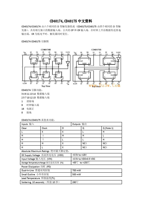
CD40174,CD40175中文资料
VDD=5V
230
400
NS
VDD=10V
90
150
VDD=15V
75
120
tSU
Time Prior to Clock Pulse that
Data must be Present
VDD=5V
45
100
NS
VDD=10V
15
40
VDD=15V
VDD=5V
1=10V
75
110
VDD=15V
60
90
tPHL
Propagation Delay Time to a
Logical “0” from Clear to Q
VDD=5V
180
300
NS
VDD=10V
70
110
VDD=15V
60
90
tPLH
Propagation Delay Time to a Logical
CD40174,CD40175中文资料
CD40174/CC40174由六个相同的D型触发器组成(CD40175/CC40175由四个相同的D型触发器)。具有相互独立的数据输入端、公共的CP和CR输入端,在时钟上升沿数据传送到Q输出端。CR为低电平时,触发器同时复位。
CD40174 CD40175引脚图
13
35
tH
Time after Clock Pulse that
Data Must be Held
VDD=5V
VDD=10V
-11
0
NS
-4
0
VDD=15V
CD4017中文资料内容说明及其运用

CD4017中文资料内容说明及其运用电子制作2009-11-14 20:09:21 阅读5119 评论1 字号:大中小订阅cd4017中文资料内容说明cd4017中文资料内容说明:CD4017 是5 位Johnson 计数器,具有10 个译码输出端,CP、CR、INH 输入端。
时钟输入端的斯密特触发器具有脉冲整形功能,对输入时钟脉冲上升和下降时间无限制。
INH 为低电平时,计数器在时钟上升沿计数;反之,计数功能无效。
CR 为高电平时,计数器清零。
Johnson 计数器,提供了快速操作、2 输入译码选通和无毛刺译码输出。
防锁选通,保证了正确的计数顺序。
译码输出一般为低电平,只有在对应时钟周期内保持高电平。
在每10 个时钟输入周期CO 信号完成一次进位,并用作多级计数链的下级脉动时钟。
CD4017 提供了16 引线多层陶瓷双列直插(D)、熔封陶瓷双列直插(J)、塑料双列直插(P)和陶瓷片状载体(C)4 种封装形式。
引出端功能符号CO:进位脉冲输渊CP:时钟输入端CR:清除端INH:禁止端Q0-Q9 计数脉冲输出端VDD:正电源VSS:地CD4017组成的防抖动触摸开关电路这是一个实用点触发电路,可以方便的与各种电路组合使用,温度控制,光控,声控,射频遥控。
而只需把这些信号加到CD4017的CP端。
本电路使用一片十进制计数器CD4017,输出Y2和复位端RST相接,14脚每次到两个记数脉冲既复位。
其工作原理是220伏交流电经变压器降压、D1-D4整流、C1滤波后获得+9V直流电压。
C3、R2构成上电复位电路,CD4017复位后Y0输出高电平,Y1和Y2输出低电平,三极管V导通。
继电器吸合,其常开触点接通用电器。
K被按下后,C2迅速放电,14脚获得脉冲上升沿,触发CD4017记数,使Y0输出低电平,Y2仍保持低电平。
此时三极管V截止,继电器释放,用电器断电。
再次按下K时,C2再次放电,14脚又获得一个记数脉冲,CD4017的Y0和Y1输出低电平,Y2输出高电平,通过二极管D5将CD4017复位,Y0 输出高电平,Y1和Y2输出低电平,三极管V再次导通,继电器吸合。
CD40175BD中文资料
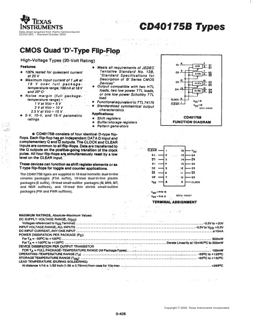
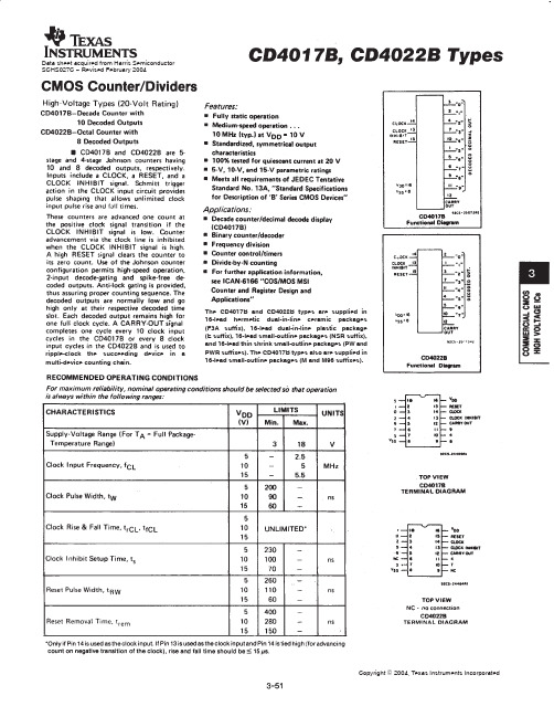
The CD40175B types are supplied in 16-lead hermetic dual-in-line ceramic packages (F3A suffix), 16-lead dual-in-line plastic packages (E suffix), 16-lead small-outline packages (M, M96, MT ,and NSR suffixes), and 16-lead thin shrink small-outline packages (PW and PWR suffixes).Data sheet acquired from Harris Semiconductor SCHS105C − Revised October 2003PACKAGING INFORMATIONOrderable Device Status(1)PackageType PackageDrawingPins PackageQtyEco Plan(2)Lead/Ball Finish MSL Peak Temp(3)CD40175BE ACTIVE PDIP N1625Pb-Free(RoHS)CU NIPDAU N/A for Pkg TypeCD40175BEE4ACTIVE PDIP N1625Pb-Free(RoHS)CU NIPDAU N/A for Pkg Type CD40175BF3A ACTIVE CDIP J161TBD A42SNPB N/A for Pkg Type CD40175BM ACTIVE SOIC D1640Green(RoHS&no Sb/Br)CU NIPDAU Level-1-260C-UNLIMCD40175BM96ACTIVE SOIC D162500Green(RoHS&no Sb/Br)CU NIPDAU Level-1-260C-UNLIMCD40175BM96E4ACTIVE SOIC D162500Green(RoHS&no Sb/Br)CU NIPDAU Level-1-260C-UNLIMCD40175BM96G4ACTIVE SOIC D162500Green(RoHS&no Sb/Br)CU NIPDAU Level-1-260C-UNLIMCD40175BME4ACTIVE SOIC D1640Green(RoHS&no Sb/Br)CU NIPDAU Level-1-260C-UNLIMCD40175BMG4ACTIVE SOIC D1640Green(RoHS&no Sb/Br)CU NIPDAU Level-1-260C-UNLIMCD40175BMT ACTIVE SOIC D16250Green(RoHS&no Sb/Br)CU NIPDAU Level-1-260C-UNLIMCD40175BMTE4ACTIVE SOIC D16250Green(RoHS&no Sb/Br)CU NIPDAU Level-1-260C-UNLIMCD40175BMTG4ACTIVE SOIC D16250Green(RoHS&no Sb/Br)CU NIPDAU Level-1-260C-UNLIMCD40175BNSR ACTIVE SO NS162000Green(RoHS&no Sb/Br)CU NIPDAU Level-1-260C-UNLIMCD40175BNSRE4ACTIVE SO NS162000Green(RoHS&no Sb/Br)CU NIPDAU Level-1-260C-UNLIMCD40175BNSRG4ACTIVE SO NS162000Green(RoHS&no Sb/Br)CU NIPDAU Level-1-260C-UNLIMCD40175BPW ACTIVE TSSOP PW1690Green(RoHS&no Sb/Br)CU NIPDAU Level-1-260C-UNLIMCD40175BPWE4ACTIVE TSSOP PW1690Green(RoHS&no Sb/Br)CU NIPDAU Level-1-260C-UNLIMCD40175BPWG4ACTIVE TSSOP PW1690Green(RoHS&no Sb/Br)CU NIPDAU Level-1-260C-UNLIMCD40175BPWR ACTIVE TSSOP PW162000Green(RoHS&no Sb/Br)CU NIPDAU Level-1-260C-UNLIMCD40175BPWRE4ACTIVE TSSOP PW162000Green(RoHS&no Sb/Br)CU NIPDAU Level-1-260C-UNLIMCD40175BPWRG4ACTIVE TSSOP PW162000Green(RoHS&no Sb/Br)CU NIPDAU Level-1-260C-UNLIMCD40175BW OBSOLETE WAFERSALEYS0TBD Call TI Call TI(1)The marketing status values are defined as follows:ACTIVE:Product device recommended for new designs.LIFEBUY:TI has announced that the device will be discontinued,and a lifetime-buy period is in effect.NRND:Not recommended for new designs.Device is in production to support existing customers,but TI does not recommend using this part in a new design.PREVIEW:Device has been announced but is not in production.Samples may or may not be available.OBSOLETE:TI has discontinued the production of the device.(2)Eco Plan-The planned eco-friendly classification:Pb-Free(RoHS),Pb-Free(RoHS Exempt),or Green(RoHS&no Sb/Br)-please check /productcontent for the latest availability information and additional product content details.TBD:The Pb-Free/Green conversion plan has not been defined.Pb-Free(RoHS):TI's terms"Lead-Free"or"Pb-Free"mean semiconductor products that are compatible with the current RoHS requirements for all6substances,including the requirement that lead not exceed0.1%by weight in homogeneous materials.Where designed to be soldered at high temperatures,TI Pb-Free products are suitable for use in specified lead-free processes.Pb-Free(RoHS Exempt):This component has a RoHS exemption for either1)lead-based flip-chip solder bumps used between the die and package,or2)lead-based die adhesive used between the die and leadframe.The component is otherwise considered Pb-Free(RoHS compatible)as defined above.Green(RoHS&no Sb/Br):TI defines"Green"to mean Pb-Free(RoHS compatible),and free of Bromine(Br)and Antimony(Sb)based flame retardants(Br or Sb do not exceed0.1%by weight in homogeneous material)(3)MSL,Peak Temp.--The Moisture Sensitivity Level rating according to the JEDEC industry standard classifications,and peak solder temperature.Important Information and Disclaimer:The information provided on this page represents TI's knowledge and belief as of the date that it is provided.TI bases its knowledge and belief on information provided by third parties,and makes no representation or warranty as to the accuracy of such information.Efforts are underway to better integrate information from third parties.TI has taken and continues to take reasonable steps to provide representative and accurate information but may not have conducted destructive testing or chemical analysis on incoming materials and chemicals.TI and TI suppliers consider certain information to be proprietary,and thus CAS numbers and other limited information may not be available for release.In no event shall TI's liability arising out of such information exceed the total purchase price of the TI part(s)at issue in this document sold by TI to Customer on an annual basis.TAPE AND REEL INFORMATION*All dimensions are nominalDevicePackage Type Package Drawing Pins SPQReel Diameter (mm)Reel Width W1(mm)A0(mm)B0(mm)K0(mm)P1(mm)W (mm)Pin1Quadrant CD40175BM96SOIC D 162500330.016.4 6.510.3 2.18.016.0Q1CD40175BNSR SO NS 162000330.016.48.210.5 2.512.016.0Q1CD40175BPWRTSSOPPW162000330.012.47.05.61.68.012.0Q1*All dimensions are nominalDevice Package Type Package Drawing Pins SPQ Length(mm)Width(mm)Height(mm) CD40175BM96SOIC D162500333.2345.928.6 CD40175BNSR SO NS162000346.0346.033.0 CD40175BPWR TSSOP PW162000346.0346.029.0IMPORTANT NOTICETexas Instruments Incorporated and its subsidiaries(TI)reserve the right to make corrections,modifications,enhancements,improvements, and other changes to its products and services at any time and to discontinue any product or service without notice.Customers should obtain the latest relevant information before placing orders and should verify that such information is current and complete.All products are sold subject to TI’s terms and conditions of sale supplied at the time of order acknowledgment.TI warrants performance of its hardware products to the specifications applicable at the time of sale in accordance with TI’s standard warranty.Testing and other quality control techniques are used to the extent TI deems necessary to support this warranty.Except where mandated by government requirements,testing of all parameters of each product is not necessarily performed.TI assumes no liability for applications assistance or customer product design.Customers are responsible for their products and applications using TI components.To minimize the risks associated with customer products and applications,customers should provide adequate design and operating safeguards.TI does not warrant or represent that any license,either express or implied,is granted under any TI patent right,copyright,mask work right, or other TI intellectual property right relating to any combination,machine,or process in which TI products or services are rmation published by TI regarding third-party products or services does not constitute a license from TI to use such products or services or a warranty or endorsement e of such information may require a license from a third party under the patents or other intellectual property of the third party,or a license from TI under the patents or other intellectual property of TI.Reproduction of TI information in TI data books or data sheets is permissible only if reproduction is without alteration and is accompanied by all associated warranties,conditions,limitations,and notices.Reproduction of this information with alteration is an unfair and deceptive business practice.TI is not responsible or liable for such altered rmation of third parties may be subject to additional restrictions.Resale of TI products or services with statements different from or beyond the parameters stated by TI for that product or service voids all express and any implied warranties for the associated TI product or service and is an unfair and deceptive business practice.TI is not responsible or liable for any such statements.TI products are not authorized for use in safety-critical applications(such as life support)where a failure of the TI product would reasonably be expected to cause severe personal injury or death,unless officers of the parties have executed an agreement specifically governing such use.Buyers represent that they have all necessary expertise in the safety and regulatory ramifications of their applications,and acknowledge and agree that they are solely responsible for all legal,regulatory and safety-related requirements concerning their products and any use of TI products in such safety-critical applications,notwithstanding any applications-related information or support that may be provided by TI.Further,Buyers must fully indemnify TI and its representatives against any damages arising out of the use of TI products in such safety-critical applications.TI products are neither designed nor intended for use in military/aerospace applications or environments unless the TI products are specifically designated by TI as military-grade or"enhanced plastic."Only products designated by TI as military-grade meet military specifications.Buyers acknowledge and agree that any such use of TI products which TI has not designated as military-grade is solely at the Buyer's risk,and that they are solely responsible for compliance with all legal and regulatory requirements in connection with such use. TI products are neither designed nor intended for use in automotive applications or environments unless the specific TI products are designated by TI as compliant with ISO/TS16949requirements.Buyers acknowledge and agree that,if they use any non-designated products in automotive applications,TI will not be responsible for any failure to meet such requirements.Following are URLs where you can obtain information on other Texas Instruments products and application solutions:Products ApplicationsAmplifiers AudioData Converters AutomotiveDSP BroadbandClocks and Timers Digital ControlInterface MedicalLogic MilitaryPower Mgmt Optical NetworkingMicrocontrollers SecurityRFID TelephonyRF/IF and ZigBee®Solutions Video&ImagingWirelessMailing Address:Texas Instruments,Post Office Box655303,Dallas,Texas75265Copyright©2008,Texas Instruments Incorporated。
CD4017中文资料_数据手册_参数
-55 to 125 -55 to 125
-55 to 125
Level-1-260C-UNLIM -55 to 125
Level-1-260C-UNLIM -55 to 125
Level-1-260C-UNLIM -55 to 125
Level-1-260C-UNLIM -55 to 125
Level-1-260C-UNLIM -55 to 125
Device Marking
(4/5)
CD4017BE CD4017BE CD4017BF CD4017BF3A
CD4017BM CD4017BM CD4017BM CD4017BM CD4017B CD4017B CM017B CM017B CM017B CM017B CD4022BE CD4022BE
(1)
Drawing
Qty
OBSOLETE
0
ACTIVE
PDIP
N
16
25
ACTIVE
PDIP
N
16
25
ACTIVE
CDIP
J
16
1
Eco Plan
(2)
TBD
Pb-Free (RoHS)
Pb-Free (RoHS)
TBD
ACTIVE
CDIP
J
16
1
TBD
OBSOLETE ACTIVE
CDIP SOIC
Samples
Addendum-Page 1
PACKAGE OPTION ADDENDUM
10-Jun-2014
Orderable Device CD4022BF
CD4022BF3A CD4022BNSR CD4022BNSRE4 CD4022BPW CD4022BPWE4 CD4022BPWR CD4022BPWRE4 CD4022BPWRG4 JM38510/05651BEA M38510/05651BEA
cd4017管脚图引脚功能内部结构应用参数
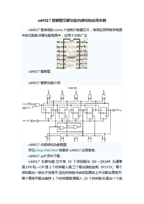
cd4017管脚图引脚功能内部结构应用参数
cd4017是常用的coms十进制计数器芯片,常用在各种数字电路中的记数脉冲等功能电路中,应用十分的广泛.
cd4017管脚图
cd4017管脚功能介绍:
cd4017内部结构功能框图
详见/chip/266.html有更多cd4017应用参数.
cd4017 pdf 资料下载:
cd4017引脚功能:芯片有10个译码输出Q0~Q9;MR为清零端,CP0和~CPl是2个时钟输入端,三个输出端的控制. 0Y1Y2Y。
每个译码输出一般处于低电平,且在时钟脉冲由低到高的上升沿输出高电平;每个高电平输出维持1个时钟周期;每输入10个时钟脉冲,输出一个进
位脉冲,因而进位输出信号可作为下一级计数器的时钟信号.在清零输入端(R)加高电平或正脉冲时,只有输出端Q0为高电平,其余各输出端都为低电平"0".。
CD4017中文资料

Recommended Operating Conditions 建议操作条件: DC Supply Voltage 直流供电电压 (VDD) Input Voltage 输入电压 (VIN) Operating Temperature Range 工作温度范围 (TA) DC Electrical Characteristics 直流电气特性: Symbol 符号 Parameter 参数 Conditions 条件 VDD = 5V IDD Quiescent Device Current 静态电流 VDD = 10V VDD = 15V |IO| < 1.0 μA LOW Level Output VOL Voltage 输出低电 平电压 VDD = 5V VDD = 10V VDD = 15V |IO| < 1.0 μA HIGH Level Output VOH Voltage 输出高电 平电压 VDD = 5V VDD = 10V VDD = 15V |IO| < 1.0 μA VDD = 5V, VO = 0.5V LOW Level Input or 4.5V VIL Voltage 输入低电 VDD = 10V, VO = 平电压 1.0V or 9.0V VDD = 15V, VO = 1.5V or 13.5V |IO| < 1.0 μA VDD = 5V, VO = 0.5V HIGH Level Input or 4.5V VIH Voltage 输入高电 VDD = 10V, VO = 平电压 1.0V or 9.0V VDD = 15V, VO = 1.5V or 13.5V 3.5 7.0 11.0 3.5 7.0 11.0 0.44 0.88 1.1 3.0 2.25 8.8 3.5 7.0 11.0 0.36 0.9 2.4 -0.12 mA mA V 1.5 3.0 4.0 1.5 3.0 4.0 1.5 3.0 4.0 V 4.95 9.95 14.95 4.95 5 9.95 10 14.95 15 4.95 9.95 14.95 V 0.05 0.05 0.05 0 0 0 0.05 0.05 0.05 0.05 0.05 0.05 V -40℃ +25° 最大 20 40 80 +85℃ 最小 150 300 600 μA 最大 Units 单位 +3 VDC to +15 VDC 0 to VDD VDC -40℃ to +85℃
4017芯片

数字电路CD4017的原理及应用电路2008/10/18 00:26数字电路CD4017是十进制计数/分频器,它的内部由计数器及译码器两部分组成,由译码输出实现对脉冲信号的分配,整个输出时序就是Q0、Q1、Q2、…、Q9依次出现与时钟同步的高电平,宽度等于时钟周期。
CD4017有10个输出端(Q0~Q9)和1个进位输出端~Q5-9。
每输入10个计数脉冲,~Q5-9就可得到1个进位正脉冲,该进位输出信号可作为下一级的时钟信号。
CD4017有3个输(MR、CP0和~CP1),MR为清零端,当在MR端上加高电平或正脉冲时其输出Q0为高电平,其余输出端(Q1~Q9)均为低电平。
CP0和~CPl是2个时钟输入端,若要用上升沿来计数,则信号由CP0端输入;若要用下降沿来计数,则信号由~CPl端输入。
设置2个时钟输入端,级联时比较方便,可驱动更多二极管发光。
由此可见,当CD4017有连续脉冲输入时,其对应的输出端依次变为高电平状态,故可直接用作顺序脉冲发生器。
CD4017有两个时钟端 CP 和 EN,若用时钟脉冲的上沿计数,则信号从 CP 端输入;若用下降沿计数,则信号从 EN 端输入。
设置两个时钟端是为了级联方便。
CD4017 与 CD4022 是一对姊妹产品,主要区别是 CD4022 是八进制的,所以译码输出仅有 Y0~Y7,每输入 8 个脉冲周期,就可得到一个进位输出,它们的管脚相同,不过 CD4022 的 6、9 脚是空脚。
cd4017方框图 cd4017引脚图一、用一个CD4017制成的彩灯电路1.用一个CD4017制作的彩灯电路如图1 所示。
cd4017电路图2.电路工作原理CD4017输出高电平的顺序分别是③、②、④、⑦、⑩、①、⑤、⑥、⑨脚,故③、②、④、⑦、⑩、①脚的高电平使6串彩灯向右顺序发光,⑤、⑥、③脚的高电平使6串彩灯由中心向两边散开发光。
各种发光方式可按自己的需要进行具体的组合,若要改变彩灯的闪光速度,可改变电容C1的大小。
4017 详细功能

CD4017引脚功能参数图,电路图,原理图资料十进制计数/分频器CD4017,其内部由计数器及译码器两部分组成,由译码输出实现对脉冲信号的分配,整个输出时序就是O0、O1、O2、…、O9依次出现与时钟同步的高电平,宽度等于时钟周期。
CD4017有10个输出端(O0~O9)和1个进位输出端~O5-9。
每输入10个计数脉冲,~O5-9就可得到1个进位正脉冲,该进位输出信号可作为下一级的时钟信号。
CD4017有3个输(MR、CP0和~CP1),MR为清零端,当在MR端上加高电平或正脉冲时其输出O0为高电平,其余输出端(O1~O9)均为低电平。
CP0和~CPl是2个时钟输入端,若要用上升沿来计数,则信号由CP0端输入;若要用下降沿来计数,则信号由~CPl端输入。
设置2个时钟输入端,级联时比较方便,可驱动更多二极管发光。
由此可见,当CD4017有连续脉冲输入时,其对应的输出端依次变为高电平状态,故可直接用作顺序脉冲发生器。
此主题相关图片如下:1111.jpgCD4017引脚图一、用一个CD4017制成的彩灯电路1.用一个CD4017制作的彩灯电路如图1所示。
此主题相关图片如下:222.jpg2.电路工作原理CD4017输出高电平的顺序分别是③、②、④、⑦、⑩、①、⑤、⑥、⑨脚,故③、②、④、⑦、⑩、①脚的高电平使6串彩灯向右顺序发光,⑤、⑥、③脚的高电平使6串彩灯由中心向两边散开发光。
各种发光方式可按自己的需要进行具体的组合,若要改变彩灯的闪光速度,可改变电容C1的大小。
二、用三个CD4O17彩灯电路图CD4017的级连,如图2所示。
此主题相关图片如下:3333.gifCD4017原理图电路2.CD4017级连后可以顺序输出24个高电平,同上理可组合出各种不同的发光方式,见图3,可使6串彩灯向右流水发光,再向左流水发光,中心向两边散开后再向中心靠拢发光,1、3、5、2、4、6串间隔发光等等cd4017是常用的coms十进制计数器芯片,常用在各种数字电路中的记数脉冲等功能电路中,应用十分的广泛.〈cd4017管脚图〉cd4017管脚功能介绍:<cd4017内部结构功能框图>详见/chip/266.html 有更多cd4017应用参数.cd4017 pdf 资料下载:/view.jsp?Searchword=cd4017cd4017引脚功能:芯片有10个译码输出Q0~Q9;MR为清零端,CP0和~CPl是2个时钟输入端,三个输出端的控制. 0Y1Y2Y。
CD4017BMG4中文资料

Data sheet acquired from Harris Semiconductor SCHS027C − Revised February 2004The CD4017B and CD4022B types are supplied in 16-lead hermetic dual-in-line ceramic packages (F3A suffix), 16-lead dual-in-line plastic package (E suffix), 16-lead small-outline packages (NSR suffix),and 16-lead thin shrink small-outline packages (PW and PWR suffixes). The CD4017B types also are supplied in 16-lead small-outline packages (M and M96 suffixes).ripple-clock the succeeding device in a multi-device counting chain.PACKAGING INFORMATIONOrderable Device Status(1)PackageType PackageDrawingPins PackageQtyEco Plan(2)Lead/Ball Finish MSL Peak Temp(3)89270AKB3T OBSOLETE0TBD Call TI Call TICD4017BE ACTIVE PDIP N1625Pb-Free(RoHS)CU NIPDAU N/A for Pkg TypeCD4017BEE4ACTIVE PDIP N1625Pb-Free(RoHS)CU NIPDAU N/A for Pkg Type CD4017BF ACTIVE CDIP J161TBD A42SNPB N/A for Pkg Type CD4017BF3A ACTIVE CDIP J161TBD A42SNPB N/A for Pkg Type CD4017BF3AS2534OBSOLETE CDIP J16TBD Call TI Call TI CD4017BM ACTIVE SOIC D1640Green(RoHS&no Sb/Br)CU NIPDAU Level-1-260C-UNLIMCD4017BM96ACTIVE SOIC D162500Green(RoHS&no Sb/Br)CU NIPDAU Level-1-260C-UNLIMCD4017BM96E4ACTIVE SOIC D162500Green(RoHS&no Sb/Br)CU NIPDAU Level-1-260C-UNLIMCD4017BM96G4ACTIVE SOIC D162500Green(RoHS&no Sb/Br)CU NIPDAU Level-1-260C-UNLIMCD4017BME4ACTIVE SOIC D1640Green(RoHS&no Sb/Br)CU NIPDAU Level-1-260C-UNLIMCD4017BMG4ACTIVE SOIC D1640Green(RoHS&no Sb/Br)CU NIPDAU Level-1-260C-UNLIMCD4017BNSR ACTIVE SO NS162000Green(RoHS&no Sb/Br)CU NIPDAU Level-1-260C-UNLIMCD4017BNSRE4ACTIVE SO NS162000Green(RoHS&no Sb/Br)CU NIPDAU Level-1-260C-UNLIMCD4017BNSRG4ACTIVE SO NS162000Green(RoHS&no Sb/Br)CU NIPDAU Level-1-260C-UNLIMCD4017BPW ACTIVE TSSOP PW1690Green(RoHS&no Sb/Br)CU NIPDAU Level-1-260C-UNLIMCD4017BPWE4ACTIVE TSSOP PW1690Green(RoHS&no Sb/Br)CU NIPDAU Level-1-260C-UNLIMCD4017BPWG4ACTIVE TSSOP PW1690Green(RoHS&no Sb/Br)CU NIPDAU Level-1-260C-UNLIMCD4017BPWR ACTIVE TSSOP PW162000Green(RoHS&no Sb/Br)CU NIPDAU Level-1-260C-UNLIMCD4017BPWRE4ACTIVE TSSOP PW162000Green(RoHS&no Sb/Br)CU NIPDAU Level-1-260C-UNLIMCD4017BPWRG4ACTIVE TSSOP PW162000Green(RoHS&no Sb/Br)CU NIPDAU Level-1-260C-UNLIMCD4022BE ACTIVE PDIP N1625Pb-Free(RoHS)CU NIPDAU N/A for Pkg TypeCD4022BEE4ACTIVE PDIP N1625Pb-Free(RoHS)CU NIPDAU N/A for Pkg Type CD4022BF ACTIVE CDIP J161TBD A42SNPB N/A for Pkg Type CD4022BF3A ACTIVE CDIP J161TBD A42SNPB N/A for Pkg Type CD4022BNSR ACTIVE SO NS162000Green(RoHS&no Sb/Br)CU NIPDAU Level-1-260C-UNLIMCD4022BNSRE4ACTIVE SO NS162000Green(RoHS&no Sb/Br)CU NIPDAU Level-1-260C-UNLIMOrderable Device Status(1)PackageType PackageDrawingPins PackageQtyEco Plan(2)Lead/Ball Finish MSL Peak Temp(3)CD4022BNSRG4ACTIVE SO NS162000Green(RoHS&no Sb/Br)CU NIPDAU Level-1-260C-UNLIMCD4022BPW ACTIVE TSSOP PW1690Green(RoHS&no Sb/Br)CU NIPDAU Level-1-260C-UNLIMCD4022BPWE4ACTIVE TSSOP PW1690Green(RoHS&no Sb/Br)CU NIPDAU Level-1-260C-UNLIMCD4022BPWG4ACTIVE TSSOP PW1690Green(RoHS&no Sb/Br)CU NIPDAU Level-1-260C-UNLIMCD4022BPWR ACTIVE TSSOP PW162000Green(RoHS&no Sb/Br)CU NIPDAU Level-1-260C-UNLIMCD4022BPWRE4ACTIVE TSSOP PW162000Green(RoHS&no Sb/Br)CU NIPDAU Level-1-260C-UNLIMCD4022BPWRG4ACTIVE TSSOP PW162000Green(RoHS&no Sb/Br)CU NIPDAU Level-1-260C-UNLIM JM38510/05651BEA ACTIVE CDIP J161TBD A42SNPB N/A for Pkg Type (1)The marketing status values are defined as follows:ACTIVE:Product device recommended for new designs.LIFEBUY:TI has announced that the device will be discontinued,and a lifetime-buy period is in effect.NRND:Not recommended for new designs.Device is in production to support existing customers,but TI does not recommend using this part in a new design.PREVIEW:Device has been announced but is not in production.Samples may or may not be available.OBSOLETE:TI has discontinued the production of the device.(2)Eco Plan-The planned eco-friendly classification:Pb-Free(RoHS),Pb-Free(RoHS Exempt),or Green(RoHS&no Sb/Br)-please check /productcontent for the latest availability information and additional product content details.TBD:The Pb-Free/Green conversion plan has not been defined.Pb-Free(RoHS):TI's terms"Lead-Free"or"Pb-Free"mean semiconductor products that are compatible with the current RoHS requirements for all6substances,including the requirement that lead not exceed0.1%by weight in homogeneous materials.Where designed to be soldered at high temperatures,TI Pb-Free products are suitable for use in specified lead-free processes.Pb-Free(RoHS Exempt):This component has a RoHS exemption for either1)lead-based flip-chip solder bumps used between the die and package,or2)lead-based die adhesive used between the die and leadframe.The component is otherwise considered Pb-Free(RoHS compatible)as defined above.Green(RoHS&no Sb/Br):TI defines"Green"to mean Pb-Free(RoHS compatible),and free of Bromine(Br)and Antimony(Sb)based flame retardants(Br or Sb do not exceed0.1%by weight in homogeneous material)(3)MSL,Peak Temp.--The Moisture Sensitivity Level rating according to the JEDEC industry standard classifications,and peak solder temperature.Important Information and Disclaimer:The information provided on this page represents TI's knowledge and belief as of the date that it is provided.TI bases its knowledge and belief on information provided by third parties,and makes no representation or warranty as to the accuracy of such information.Efforts are underway to better integrate information from third parties.TI has taken and continues to take reasonable steps to provide representative and accurate information but may not have conducted destructive testing or chemical analysis on incoming materials and chemicals.TI and TI suppliers consider certain information to be proprietary,and thus CAS numbers and other limited information may not be available for release.In no event shall TI's liability arising out of such information exceed the total purchase price of the TI part(s)at issue in this document sold by TI to Customer on an annual basis.TAPE AND REEL INFORMATION*All dimensions are nominalDevicePackage Type Package Drawing Pins SPQReel Diameter (mm)Reel Width W1(mm)A0(mm)B0(mm)K0(mm)P1(mm)W (mm)Pin1Quadrant CD4017BM96SOIC D 162500330.016.4 6.510.3 2.18.016.0Q1CD4017BNSR SO NS 162000330.016.48.210.5 2.512.016.0Q1CD4017BPWR TSSOP PW 162000330.012.47.0 5.6 1.68.012.0Q1CD4022BNSR SO NS 162000330.016.48.210.5 2.512.016.0Q1CD4022BPWRTSSOPPW162000330.012.47.05.61.68.012.0Q1*All dimensions are nominalDevice Package Type Package Drawing Pins SPQ Length(mm)Width(mm)Height(mm) CD4017BM96SOIC D162500333.2345.928.6 CD4017BNSR SO NS162000346.0346.033.0 CD4017BPWR TSSOP PW162000346.0346.029.0 CD4022BNSR SO NS162000346.0346.033.0 CD4022BPWR TSSOP PW162000346.0346.029.0IMPORTANT NOTICETexas Instruments Incorporated and its subsidiaries(TI)reserve the right to make corrections,modifications,enhancements,improvements, and other changes to its products and services at any time and to discontinue any product or service without notice.Customers should obtain the latest relevant information before placing orders and should verify that such information is current and complete.All products are sold subject to TI’s terms and conditions of sale supplied at the time of order acknowledgment.TI warrants performance of its hardware products to the specifications applicable at the time of sale in accordance with TI’s standard warranty.Testing and other quality control techniques are used to the extent TI deems necessary to support this warranty.Except where mandated by government requirements,testing of all parameters of each product is not necessarily performed.TI assumes no liability for applications assistance or customer product design.Customers are responsible for their products and applications using TI components.To minimize the risks associated with customer products and applications,customers should provide adequate design and operating safeguards.TI does not warrant or represent that any license,either express or implied,is granted under any TI patent right,copyright,mask work right, or other TI intellectual property right relating to any combination,machine,or process in which TI products or services are rmation published by TI regarding third-party products or services does not constitute a license from TI to use such products or services or a warranty or endorsement e of such information may require a license from a third party under the patents or other intellectual property of the third party,or a license from TI under the patents or other intellectual property of TI.Reproduction of TI information in TI data books or data sheets is permissible only if reproduction is without alteration and is accompanied by all associated warranties,conditions,limitations,and notices.Reproduction of this information with alteration is an unfair and deceptive business practice.TI is not responsible or liable for such altered rmation of third parties may be subject to additional restrictions.Resale of TI products or services with statements different from or beyond the parameters stated by TI for that product or service voids all express and any implied warranties for the associated TI product or service and is an unfair and deceptive business practice.TI is not responsible or liable for any such statements.TI products are not authorized for use in safety-critical applications(such as life support)where a failure of the TI product would reasonably be expected to cause severe personal injury or death,unless officers of the parties have executed an agreement specifically governing such use.Buyers represent that they have all necessary expertise in the safety and regulatory ramifications of their applications,and acknowledge and agree that they are solely responsible for all legal,regulatory and safety-related requirements concerning their products and any use of TI products in such safety-critical applications,notwithstanding any applications-related information or support that may be provided by TI.Further,Buyers must fully indemnify TI and its representatives against any damages arising out of the use of TI products in such safety-critical applications.TI products are neither designed nor intended for use in military/aerospace applications or environments unless the TI products are specifically designated by TI as military-grade or"enhanced plastic."Only products designated by TI as military-grade meet military specifications.Buyers acknowledge and agree that any such use of TI products which TI has not designated as military-grade is solely at the Buyer's risk,and that they are solely responsible for compliance with all legal and regulatory requirements in connection with such use. TI products are neither designed nor intended for use in automotive applications or environments unless the specific TI products are designated by TI as compliant with ISO/TS16949requirements.Buyers acknowledge and agree that,if they use any non-designated products in automotive applications,TI will not be responsible for any failure to meet such requirements.Following are URLs where you can obtain information on other Texas Instruments products and application solutions:Products ApplicationsAmplifiers AudioData Converters AutomotiveDSP BroadbandClocks and Timers Digital ControlInterface MedicalLogic MilitaryPower Mgmt Optical NetworkingMicrocontrollers SecurityRFID TelephonyRF/IF and ZigBee®Solutions Video&ImagingWirelessMailing Address:Texas Instruments,Post Office Box655303,Dallas,Texas75265Copyright©2008,Texas Instruments Incorporated。
cd4017工作原理详解(cd4017引脚图及功能
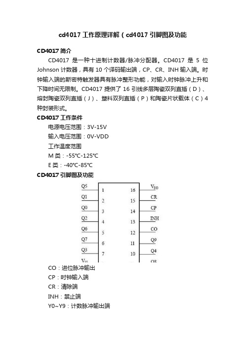
cd4017工作原理详解(cd4017引脚图及功能CD4017简介CD4017是一种十进制计数器/脉冲分配器。
CD4017是5位Johnson计数器,具有10个译码输出端,CP、CR、INH输入端。
时钟输入端的斯密特触发器具有脉冲整形功能,对输入时钟脉冲上升和下降时间无限制。
CD4017提供了16引线多层陶瓷双列直插(D)、熔封陶瓷双列直插(J)、塑料双列直插(P)和陶瓷片状载体(C)4种封装形式。
CD4017工作条件电源电压范围:3V-15V输入电压范围:0V-VDD工作温度范围M类:-55℃-125℃E类:-40℃-85℃CD4017引脚图及功能CO:进位脉冲输出CP:时钟输入端CR:清除端INH:禁止端Y0~Y9:计数脉冲输出端VDD:正电源VSS:地CD4017真值表cd4017工作原理cd4017计数器,提供了快速操作、2 输入译码选通和无毛刺译码输出。
防锁选通,保证了正确的计数顺序。
译码输出一般为低电平,只有在对应时钟周期内保持高电平。
在每10 个时钟输入周期CO 信号完成一次进位,并用作多级计数链的下级脉动时钟。
CD4017内部结构图图 2 CD4017 内部逻辑电原理图CD4017内部逻辑电原理图如图2所示。
它是由十进制计数器电路和时序译码电路两部分组成。
其中的D触发器Fl~F5构成了十进制约翰逊计数器,门电路5~14 构成了时序译码电路。
约翰逊计数器的结构比较简单.它实质上是一种串行移位寄存器。
除了第3个触发器是通过门电路15、16构成的组合逻辑电路作用于F3的D3端以外,其余各级均是将前一级触发器的输出端连接到后一级触发器的输入端D的,计数器最后—级的Q5端连接到第一级的D1端。
这种计数器具有编码可靠,工作速度快、译码简单,只需由二输入瑞的与门即可译码,且译码输出无过渡脉冲干扰等特点。
通常只有译码选中的那个输出端为高电平,其余输出端均为低电平。
约翰逊计数器状态如表1-1所示。
CD4017BCNX中文资料
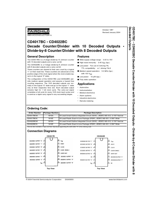
© 2004 Fairchild Semiconductor Corporation DS005950October 1987Revised January 2004CD4017BC • CD4022BC Decade Counter/Divider with 10 Decoded Outputs • Divide-by-8 Counter/Divider with 8 Decoded OutputsCD4017BC • CD4022BCDecade Counter/Divider with 10 Decoded Outputs •Divide-by-8 Counter/Divider with 8 Decoded OutputsGeneral DescriptionThe CD4017BC is a 5-stage divide-by-10 Johnson counter with 10 decoded outputs and a carry out bit.The CD4022BC is a 4-stage divide-by-8 Johnson counter with 8 decoded outputs and a carry-out bit.These counters are cleared to their zero count by a logical “1” on their reset line. These counters are advanced on the positive edge of the clock signal when the clock enable sig-nal is in the logical “0” state.The configuration of the CD4017BC and CD4022BC per-mits medium speed operation and assures a hazard free counting sequence. The 10/8 decoded outputs are nor-mally in the logical “0” state and go to the logical “1” state only at their respective time slot. Each decoded output remains high for 1 full clock cycle. The carry-out signal completes a full cycle for every 10/8 clock input cycles and is used as a ripple carry signal to any succeeding stages.Featuress Wide supply voltage range: 3.0V to 15V s High noise immunity:0.45 V DD (typ.)s Low power Fan out of 2 driving 74LTTL compatibility:or 1 driving 74LS s Medium speed operation: 5.0 MHz (typ.)with 10V V DD s Low power:10 µW (typ.)s Fully static operationApplications•Automotive •Instrumentation •Medical electronics •Alarm systems •Industrial electronics •Remote meteringOrdering Code:Devices also available in T ape and Reel. Specify by appending the suffix letter “X ” to the ordering code.Connection DiagramsCD4017BTop View CD4022BTop ViewOrder Number Package NumberPackage DescriptionCD4017BCM M16A 16-Lead Small Outline Integrated Circuit (SOIC), JEDEC MS-012, 0.150" Narrow CD4017BCN N16E 16-Lead Plastic Dual-In-Line Package (PDIP), JEDEC MS-001, 0.300" Wide CD4022BCM M16A 16-Lead Small Outline Integrated Circuit (SOIC), JEDEC MS-012, 0.150" Narrow CD4022BCNN16E16-Lead Plastic Dual-In-Line Package (PDIP), JEDEC MS-001, 0.300" Wide 2C D 4017B C • C D 4022B CLogic DiagramsCD4017BTerminal No. 8 = GND Terminal No. 16 = V DDCD4022BTerminal No. 16 = V DD Terminal No. 8 = GNDCD4017BC • CD4022BCAbsolute Maximum Ratings (Note 1)(Note 2)Recommended Operating Conditions (Note 2)Note 1: “Absolute Maximum Ratings ” are those values beyond which the safety of the device cannot be guaranteed, they are not meant to imply that the devices should be operated at these limits. The table of “Recom-mended Operating Conditions ” and “Electrical Characteristics ” provides conditions for actual device operation.Note 2: V SS = 0V unless otherwise specified.DC Electrical Characteristics (Note 2)Note 3: I OL and I OH are tested one output at a time.DC Supply Voltage (V DD )−0.5 V DC to +18 V DC Input Voltage (V IN )−0.5 V DC to V DD +0.5 V DCStorage Temperature (T S )−65°C to +150°CPower Dissipation (P D )Dual-In-Line 700 mW Small Outline 500 mWLead Temperature (T L )(Soldering, 10 seconds)260°C DC Supply Voltage (V DD )+3 V DC to +15 V DCInput Voltage (V IN )0 to V DD V DCOperating Temperature Range (T A )−55°C to +125°CSymbol ParameterConditions−55°C +25°+125°C UnitsMinMax MinTyp Max MinMax I DDQuiescent Device V DD = 5V 50.35150µACurrentV DD = 10V 100.510300V DD = 15V 20 1.020600V OLLOW Level |I O | < 1.0 µA Output VoltageV DD = 5V 0.0500.050.05VV DD = 10V 0.0500.050.05V DD = 15V0.0500.050.05V OHHIGH Level |I O | < 1.0 µA Output VoltageV DD = 5V 4.95 4.955 4.95VV DD = 10V 9.959.95109.95V DD = 15V14.9514.951514.95V ILLOW Level |I O | < 1.0 µAInput VoltageV DD = 5V, V O = 0.5V or 4.5V 1.5 1.5 1.5VV DD = 10V, V O = 1.0V or 9.0V 3.0 3.0 3.0V DD = 15V, V O = 1.5V or 13.5V4.04.0 4.0V IHHIGH Level |I O | < 1.0 µAInput VoltageV DD = 5V, V O = 0.5V or 4.5V 3.5 3.5 3.5VV DD = 10V, V O = 1.0V or 9.0V 7.07.07.0V DD = 15V, V O = 1.5V or 13.5V11.011.011.0I OLLOW Level Output V DD = 5V, V O = 0.4V 0.640.510.880.36mACurrent (Note 3)V DD = 10V, V O = 0.5V 1.6 1.3 2.250.9V DD = 15V, V O = 1.5V 4.2 3.48.8 2.4I OHHIGH Level Output V DD = 5V, V O = 4.6V −0.25−0.2−0.36−0.14mA Current (Note 3)V DD = 10V, V O = 9.5V −0.62−0.5−0.9−0.35V DD = 15V, V O = 13.5V −1.8−1.5−3.5−1.1I INInput CurrentV DD = 15V, V IN = 0V −0.1−10−5−0.1−1.0µA V DD = 15V, V IN = 15V0.110−50.11.0 4C D 4017B C • C D 4022B CAC Electrical Characteristics (Note 4)T A = 25°C, C L = 50 pF, R L = 200k, t rCL and t fCL = 20 ns, unless otherwise specified Note 4: AC Parameters are guaranteed by DC correlated testing.AC Electrical Characteristics (Note 4)T A = 25°C, C L = 50 pF, R L = 200k, t rCL and t fCL = 20 ns, unless otherwise specifiedSymbolParameter Conditions Min Typ Max UnitsCLOCK OPERATIONt PHL, t PLH Propagation Delay Time Carry Out LineV DD = 5V 415800nsV DD = 10V 160320V DD = 15V130250Carry Out LineV DD = 5V C L = 15 pF240480nsV DD = 10V 85170V DD = 15V70140Decode Out LinesV DD = 5V 5001000nsV DD = 10V 200400V DD = 15V160320t TLH , t THL Transition Time Carry Out and Decode Out Linest TLHV DD = 5V 200360nsV DD = 10V 100180V DD = 15V80130t THLV DD = 5V 100200nsV DD = 10V 50100V DD = 15V4080f CLMaximum Clock FrequencyV DD = 5V Measured with 1.02MHzV DD = 10V Respect to Carry 2.55V DD = 15VOutput Line3.06t WL , t WHMinimum Clock Pulse WidthV DD = 5V 125250ns V DD = 10V 4590V DD = 15V3570t rCL , t fCLClock Rise and Fall TimeV DD = 5V 20µs V DD = 10V 15V DD = 15V5t SUMinimum Clock Inhibit Data Setup TimeV DD = 5V 120240ns V DD = 10V 4080V DD = 15V3265C INAverage Input Capacitance57.5pF Symbol ParameterConditionsMinTypMaxUnitsRESET OPERATION t PHL, tPLHPropagation Delay Time Carry Out LineV DD = 5V 415800nsV DD = 10V 160320V DD = 15V130250Carry Out LineV DD = 5V 240480ns V DD = 10V C L = 15 pF85170V DD = 15V70140Decode Out LinesV DD = 5V 5001000ns V DD = 10V 200400V DD = 15V160320t WMinimum Reset V DD = 5V 200400ns Pulse WidthV DD = 10V 70140V DD = 15V 55110t REMMinimum Reset V DD = 5V 75150ns Removal TimeV DD = 10V 3060V DD = 15V2550CD4017BC • CD4022BCTiming DiagramsCD4017BCD4022B 6C D 4017B C • C D 4022B CPhysical Dimensionsinches (millimeters) unless otherwise noted16-Lead Small Outline Integrated Circuit (SOIC), JEDEC MS-012, 0.150" NarrowPackage Number M16A7CD4017BC • CD4022BC Decade Counter/Divider with 10 Decoded Outputs • Divide-by-8 Counter/Divider with 8 Decoded OutputsPhysical Dimensions inches (millimeters) unless otherwise noted (Continued)16-Lead Plastic Dual-In-Line Package (PDIP), JEDEC MS-001, 0.300" WidePackage Number N16EFairchild does not assume any responsibility for use of any circuitry described, no circuit patent licenses are implied and Fairchild reserves the right at any time without notice to change said circuitry and specifications.LIFE SUPPORT POLICYFAIRCHILD ’S PRODUCTS ARE NOT AUTHORIZED FOR USE AS CRITICAL COMPONENTS IN LIFE SUPPORT DEVICES OR SYSTEMS WITHOUT THE EXPRESS WRITTEN APPROVAL OF THE PRESIDENT OF FAIRCHILD SEMICONDUCTOR CORPORATION. As used herein:1.Life support devices or systems are devices or systems which, (a) are intended for surgical implant into the body, or (b) support or sustain life, and (c) whose failure to perform when properly used in accordance with instructions for use provided in the labeling, can be rea-sonably expected to result in a significant injury to the user.2. A critical component in any component of a life support device or system whose failure to perform can be rea-sonably expected to cause the failure of the life support device or system, or to affect its safety or effectiveness.。
CD40174BM中文资料
TL F 5987CD40174BM CD40174BC Hex D Flip-Flop CD40175BM CD40175BC Quad D Flip-FlopFebruary 1988CD40174BM CD40174BC Hex D Flip-Flop CD40175BM CD40175BC Quad D Flip-FlopGeneral DescriptionThe CD40174B consists of six positive-edge triggered D-type flip-flops the true outputs from each flip-flop are ex-ternally available The CD40175B consists of four positive-edge triggered D-type flip-flops both the true and comple-ment outputs from each flip-flop are externally available All flip-flops are controlled by a common clock and a com-mon clear Information at the D inputs meeting the set-up time requirements is transferred to the Q outputs on the positive-going edge of the clock pulse The clearing opera-tion enabled by a negative pulse at Clear input clears all Q outputs to logical ‘‘0’’and Qs (CD40175B only)to logical ‘‘1’’All inputs are protected from static discharge by diode clamps to V DD and V SSFeaturesY Wide supply voltage range 3V to 15V Y High noise immunity 0 45V DD (typ )YLow power TTL fan out of 2driving 74L compatibility or 1driving 74LS Y Equivalent to MC14174B MC14175B YEquivalent to MM74C174 MM74C175Connection DiagramsCD40174BDual-In-Line PackageTL F 5987–1Top ViewOrder Number CD40174B or CD40175BTruth TableInputsOutputsClear ClockD Q Q L XX L H H u H H L H uL L H H H X NC NC HLXNCNCH e High level L e Low level Xe Irrelevantue Transition from low to high level NC e No changeeQ for CD40175B onlyCD40175BDual-In-Line PackageTL F 5987–2Top ViewC 1995National Semiconductor Corporation RRD-B30M105 Printed in U S AAbsolute Maximum Ratings(Notes1 2) If Military Aerospace specified devices are required please contact the National Semiconductor Sales Office Distributors for availability and specifications DC Supply Voltage(V DD)b0 5V to a18V Input Voltage(V IN)b0 5V to V DD a0 5V DC Storage Temperature Range(T S)b65 C to a150 C Power Dissipation(P D)Dual-In-Line700mW Small Outline500mW Lead Temperature(T L)(Soldering 10seconds)260 C Recommended Operating Conditions(Note2)DC Supply Voltage(V DD)3V to15V DC Input Voltage(V IN)0V to V DD V DC Operating Temperature Range(T A)CD40XXXBM b55 C to a125 C CD40XXXBC b40 C to a85 CDC Electrical Characteristics CD40174BM CD40175BM(Note2)Symbol Parameter Conditionsb55 C a25 C a125 CUnits Min Max Min Typ Max Min MaxI DD Quiescent Device Current V DD e5V V IN e V DD or V SS1 01 030m AV DD e10V V IN e V DD or V SS2 02 060m AV DD e15V V IN e V DD or V SS4 04 0120m A V OL Low Level Output Voltage l I O l k1m AV DD e5V0 050 050 05VV DD e10V0 050 050 05VV DD e15V0 050 050 05V V OH High Level Output Voltage l I O l k1m AV DD e5V4 954 9554 95VV DD e10V9 959 95109 95VV DD e15V14 9514 951514 95V V IL Low Level Input Voltage V DD e5V V O e0 5V or4 5V1 51 51 5VV DD e10V V O e1V or9V3 03 03 0VV DD e15V V O e1 5V or13 5V4 04 04 0V V IH High Level Input Voltage V DD e5V V O e0 5V or4 5V3 53 53 5VV DD e10V V O e1V or9V7 07 07 0VV DD e15V V O e1 5V or13 5V11 011 011 0V I OL Low Level Output Current V DD e5V V O e0 4V0 640 510 880 36mA(Note3)V DD e10V V O e0 5V1 61 32 250 9mAV DD e15V V O e1 5V4 23 48 82 4mA I OH High Level Output Current V DD e5V V O e4 6V b0 64b0 51b0 8 8b0 36mA(Note3)V DD e10V V O e9 5V b1 6b1 3b2 25b0 9mAV DD e15V V O e13 5V b4 2b3 4b8 8b2 4mA I IN Input Current V DD e15V V IN e0V b0 1b10b5b0 1b1 0m AV DD e15V V IN e15V0 110b50 11 0m A DC Electrical Characteristics CD40174BC CD40175BC(Note2)Symbol Parameter Conditionsb40 C a25 C a85 CUnits Min Max Min Typ Max Min MaxI DD Quiescent Device Current V DD e5V V IN e V DD or V SS4430m AV DD e10V V IN e V DD or V SS8860m AV DD e15V V IN e V DD or V SS1616120m A Note1 ‘‘Absolute Maximum Ratings’’are those values beyond which the safety of the device cannot be guaranteed They are not meant to imply that the devices should be operated at these limits The tables of‘‘Recommended Operating Conditions’’and‘‘Electrical Characteristics’’provide conditions for actual device operationNote2 V SS e0V unless otherwise specifiedNote3 I OH and I OL are tested one output at a time2DC Electrical Characteristics CD40174BC CD40175BC(Note2)(Continued)Symbol Parameter Conditionsb40 C a25 C a85 CUnits Min Max Min Typ Max Min MaxV OL Low Level Output Voltage V DD e5V0 050 050 05VV DD e10V0 050 050 05VV DD e15V0 050 050 05VV OH High Level Output Voltage V DD e5V4 954 9554 95VV DD e10V9 959 95109 95VV DD e15V14 9514 951514 95VV IL Low Level Input Voltage V DD e5V V O e0 5V or4 5V1 51 51 5VV DD e10V V O e1V or9V3 03 03 0VV DD e15V V O e1 5V or13 5V4 04 04 0VV IH High Level Input Voltage V DD e5V V O e0 5V or4 5V3 53 53 5VV DD e10V V O e1V or9V7 07 07 0VV DD e15V V O e1 5V or13 5V11 011 011 0VI OL Low Level Output Current V DD e5V V O e0 4V0 520 440 880 36mA(Note3)V DD e10V V O e0 5V1 31 12 250 9mAV DD e15V V O e1 5V3 63 08 82 4mAI OH High Level Output Current V DD e5V V O e4 6V b0 52b0 44b0 88b0 36mA(Note3)V DD e10V V O e9 5V b1 3b1 1b2 25b0 9mAV DD e15V V O e13 5V b3 6b3 0b8 8b2 4mAI IN Input Current V DD e15V V IN e0V b0 30b10b5b0 30b1 0m AV DD e15V V IN e15V0 3010b50 301 0m A AC Electrical CharacteristicsT A e25 C C L e50pF R L e200k and t r e t f e20ns unless otherwise specifiedSymbol Parameter Conditions Min Typ Max Unitst PHL t PLH Propagation Delay Time to a V DD e5V190300ns Logical‘‘0’’or Logical‘‘1’’from V DD e10V75110nsClock to Q or Q(CD40175Only)V DD e15V6090nst PHL Propagation Delay Time to a V DD e5V180300ns Logical‘‘0’’from Clear to Q V DD e10V70110nsV DD e15V6090nst PLH Propagation Delay Time to a Logical V DD e5V230400ns ‘‘1’’from Clear to Q(CD40175Only)V DD e10V90150nsV DD e15V75120nst SU Time Prior to Clock Pulse that V DD e5V45100ns Data must be Present V DD e10V1540nsV DD e15V1335nst H Time after Clock Pulse that V DD e5V b110ns Data Must be Held V DD e10V b40nsV DD e15V b30nst THL t TLH Transition Time V DD e5V100200nsV DD e10V50100nsV DD e15V4080nst WH t WL Minimum Clock Pulse Width V DD e5V130250nsV DD e10V45100nsV DD e15V4080ns3AC Electrical CharacteristicsT A e25 C C L e50pF R L e200k and t r e t f e20ns unless otherwise specified(Continued) Symbol Parameter Conditions Min Typ Max Unitst WL Minimum Clear Pulse Width V DD e5V120250nsV DD e10V45100nsV DD e15V4080nst RCL Maximum Clock Rise Time V DD e5V15m sV DD e10V5 0m sV DD e15V5 0m st fCL Maximum Clock Fall Time V DD e5V1550m sV DD e10V5 050m sV DD e15V5 050m sf CL Maximum Clock Frequency V DD e5V2 03 5MHzV DD e10V5 010MHzV DD e15V6 012MHzC IN Input Capacitance Clear Input1015pFOther Input5 07 5pFC PD Power Dissipation Per Package(Note4)130pFAC Parameters are guaranteed by DC correlated testingNote1 ‘‘Absolute Maximum Ratings’’are those values beyond which the safety of the device cannot be guaranteed They are not meant to imply that the devices should be operated at these limits The tables of‘‘Recommended Operating Conditions’’and‘‘Electrical Characteristics’’provide conditions for actual device operationNote2 V SS e0V unless otherwise specifiedNote3 I OH and I OL are tested one output at a timeNote4 C PD determines the no load AC power consumption of any CMOS device For complete explanation see54C 74C Family Characteristics application note AN-90Switching Time WaveformsTL F 5987–3t r e t f e20ns4Physical Dimensions inches(millimeters)Ceramic Dual-In-Line Package(J)Order Number CD40174BMJ CD40174BCJ CD40175BMJ or CD40175BCJNS Package Number J16A5C D 40174B M C D 40174B C H e x D F l i p -F l o p C D 40175B M C D 40175B C Q u a d D F l i p -F l o pPhysical Dimensions inches (millimeters)(Continued)Molded Dual-In-Line Package (N)Order Number CD40174BMN CD40174BCN CD40174BMN or CD40175BCNNS Package Number N16ELIFE SUPPORT POLICYNATIONAL’S PRODUCTS ARE NOT AUTHORIZED FOR USE AS CRITICAL COMPONENTS IN LIFE SUPPORT DEVICES OR SYSTEMS WITHOUT THE EXPRESS WRITTEN APPROVAL OF THE PRESIDENT OF NATIONAL SEMICONDUCTOR CORPORATION As used herein 1 Life support devices or systems are devices or 2 A critical component is any component of a life systems which (a)are intended for surgical implant support device or system whose failure to perform can into the body or (b)support or sustain life and whose be reasonably expected to cause the failure of the life failure to perform when properly used in accordance support device or system or to affect its safety or with instructions for use provided in the labeling can effectivenessbe reasonably expected to result in a significant injury to the userNational Semiconductor National Semiconductor National Semiconductor National Semiconductor CorporationEuropeHong Kong LtdJapan Ltd1111West Bardin RoadFax (a 49)0-180-530858613th Floor Straight Block Tel 81-043-299-2309。
实验十九。十进制计数器CD4017

实验十九、十进制计数器CD4017逻辑功能测试一、实验目的1、学习用集成触发器构成计数器的方法2、掌握中规模集成计数器的使用及其测试方法3、掌握CD4017计数器的逻辑功能及使用方法二、实验预习要求1、复习有关计数器部分内容2、拟出各实验内容所需的测试记录表格3、查手册,给出并熟悉实验所用各集成的引脚排列及逻辑功能。
三、实验设备与器件1、+5V直流电源2、双踪示波器3、连续脉冲源4、单次脉冲源5、逻辑电平开关6、逻辑电平显示器7、译码显示器8、CD4017B四、实验原理1、计数器是一个用以实现计数功能的时序部件,它不仅可用来计数脉冲数,还常用作数字系统定时、分频和执行数字运算以及其他特定的逻辑功能。
计数器种类很多,按构成计数器中的各触发器是否使用一个时钟脉冲源来分,有同步计数器和异步计数器。
根据计数制的不同,分为二进制计数器,十进制计数器和任意进制计数器。
根据计数的增减趋势,又分为加法、减法和可逆计数器。
还有可预置数和可编程序功能计数器等。
目前,无论是TTL还是CMOS集成电路,都有品种较齐全的中规模集成计数器。
2、中规模十进制计数器CD4017B有清除和置数等功能,其引脚排列及逻辑符号如CD4017:十进制计数器/脉冲分配器CD4017 是5 位Johnson 计数器,具有10 个译码输出端,CP、CR、INH 输入端。
时钟输入端的斯密特触发器具有脉冲整形功能,对输入时钟脉冲上升和下降时间无限制。
INH 为低电平时,计Q1-Q9(Pin3,2,4,7,10,1,5,6,9,11),为解码后的时进制输出接脚,被计数到的值,其输出为Hi,其余为Lo 电位。
b、CARRY OUT 数器在时钟上升沿计数;反之,计数功能无效。
CR 为高电平时,计数器清零。
CD4017有16支脚,除电源脚VDD及VSS为电源接脚,输入电压范围为3–15V之外,其余接脚为:A、频率输入脚:CLOCK(Pin14),为频率信号的输入脚。
数字电路CD4017的原理及应用电路教案资料
数字电路CD4017的原理及应用电路数字电路CD4017的原理及应用电路数字电路CD4017是十进制计数/分频器,它的内部由计数器及译码器两部分组成,由译码输出实现对脉冲信号的分配,整个输出时序就是Q0、Q1、Q2、…、Q9依次出现与时钟同步的高电平,宽度等于时钟周期。
CD4017有10个输出端(Q0~Q9)和1个进位输出端~Q5-9。
每输入10个计数脉冲,~Q5-9就可得到1个进位正脉冲,该进位输出信号可作为下一级的时钟信号。
CD4017有3个输(MR、CP0和~CP1),MR为清零端,当在MR端上加高电平或正脉冲时其输出Q0为高电平,其余输出端(Q1~Q9)均为低电平。
CP0和~CPl是2个时钟输入端,若要用上升沿来计数,则信号由CP0端输入;若要用下降沿来计数,则信号由~CPl端输入。
设置2个时钟输入端,级联时比较方便,可驱动更多二极管发光。
由此可见,当CD4017有连续脉冲输入时,其对应的输出端依次变为高电平状态,故可直接用作顺序脉冲发生器。
CD4017有两个时钟端 CP 和 EN,若用时钟脉冲的上沿计数,则信号从 CP 端输入;若用下降沿计数,则信号从 EN 端输入。
设置两个时钟端是为了级联方便。
CD4017 与 CD4022 是一对姊妹产品,主要区别是 CD4022 是八进制的,所以译码输出仅有 Y0~Y7,每输入 8 个脉冲周期,就可得到一个进位输出,它们的管脚相同,不过 CD4022 的 6、9 脚是空脚。
cd4017方框图 cd4017引脚图一、用一个CD4017制成的彩灯电路1.用一个CD4017制作的彩灯电路如图 1 所示。
cd4017电路图2.电路工作原理CD4017输出高电平的顺序分别是③、②、④、⑦、⑩、①、⑤、⑥、⑨脚,故③、②、④、⑦、⑩、①脚的高电平使6串彩灯向右顺序发光,⑤、⑥、③脚的高电平使6串彩灯由中心向两边散开发光。
各种发光方式可按自己的需要进行具体的组合,若要改变彩灯的闪光速度,可改变电容C1的大小。
CD4017中文资料
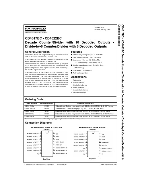
October 1987Revised January 1999CD4017BC • CD4022BC Decade Counter/Divider with 10 Decoded Outputs • Divide-by-8 Counter/Divider with 8 Decoded Outputs © 1999 Fairchild Semiconductor Corporation DS005950.prf CD4017BC • CD4022BCDecade Counter/Divider with 10 Decoded Outputs •Divide-by-8 Counter/Divider with 8 Decoded OutputsGeneral DescriptionThe CD4017BC is a 5-stage divide-by-10 Johnson counterwith 10 decoded outputs and a carry out bit.The CD4022BC is a 4-stage divide-by-8 Johnson counterwith 8 decoded outputs and a carry-out bit.These counters are cleared to their zero count by a logical“1” on their reset line. These counters are advanced on thepositive edge of the clock signal when the clock enable sig-nal is in the logical “0” state.The configuration of the CD4017BC and CD4022BC per-mits medium speed operation and assures a hazard freecounting sequence. The 10/8 decoded outputs are nor-mally in the logical “0” state and go to the logical “1” stateonly at their respective time slot. Each decoded outputremains high for 1 full clock cycle. The carry-out signalcompletes a full cycle for every 10/8 clock input cycles andis used as a ripple carry signal to any succeeding stages.Featuress Wide supply voltage range: 3.0V to 15Vs High noise immunity:0.45 V DD (typ.)s Low power Fan out of 2 driving 74LTTL compatibility:or 1 driving 74LSs Medium speed operation: 5.0 MHz (typ.)with 10V V DDs Low power:10 µW (typ.)s Fully static operationApplications•Automotive•Instrumentation•Medical electronics•Alarm systems•Industrial electronics•Remote meteringOrdering Code:Devices also available in Tape and Reel. Specify by appending the suffix letter “X” to the ordering code.Connection DiagramsPin Assignments for DIP, SOIC and SOPCD4017BTop ViewPin Assignments for DIP and SOICCD4022BTop ViewOrder Number Package Number Package DescriptionCD4017BCM M16A16-Lead Small Outline Integrated Circuit (SOIC), JEDEC MS-012, 0.150” NarrowCD4017BCSJ M16D16-Lead Small Outline Package (SOP), EIAJ TYPE II, 5.3mm WideCD4017BCN N16E16-Lead Plastic Dual-In-Line Package (PDIP), JEDEC MS-001, 0.300” WideCD4022BCM M16A16-Lead Small Outline Integrated Circuit (SOIC), JEDEC MS-012, 0.150” NarrowCD4022BCN N16E16-Lead Plastic Dual-In-Line Package (PDIP), JEDEC MS-001, 0.300” Wide 2C D 4017B C • C D 4022B CLogic DiagramsCD4017BTerminal No. 8 = GND Terminal No. 16 = V DDCD4022BTerminal No. 16 = V DD Terminal No. 8 = GNDCD4017BC • CD4022BCAbsolute Maximum Ratings (Note 1)(Note 2)Recommended Operating Conditions (Note 2)Note 1: “Absolute Maximum Ratings” are those values beyond which the safety of the device cannot be guaranteed, they are not meant to imply that the devices should be operated at these limits. The table of “Recom-mended Operating Conditions” and “Electrical Characteristics” provides conditions for actual device operation.Note 2: V SS = 0V unless otherwise specified.DC Electrical Characteristics (Note 2)Note 3: I OL and I OH are tested one output at a time.DC Supply Voltage (V DD )−0.5 V DC to +18 V DC Input Voltage (V IN )−0.5 V DC to V DD +0.5 V DCStorage Temperature (T S )−65°C to +150°CPower Dissipation (P D )Dual-In-Line 700 mW Small Outline 500 mWLead Temperature (T L )(Soldering, 10 seconds)260°C DC Supply Voltage (V DD )+3 V DC to +15 V DCInput Voltage (V IN )0 to V DD V DC Operating T emperature Range (T A )−40°C to +85°CSymbol ParameterConditions−40°C +25°+85°C Units MinMax MinTyp Max MinMax I DDQuiescent Device V DD = 5V 200.520150µA CurrentV DD = 10V 40 1.040300µA V DD = 15V 80 5.080600µA V OLLOW Level |I O | < 1.0 µA Output VoltageV DD = 5V 0.0500.050.05V V DD = 10V 0.0500.050.05V V DD = 15V0.0500.050.05V V OHHIGH Level |I O | < 1.0 µA Output VoltageV DD = 5V 4.95 4.955 4.95V V DD = 10V 9.959.95109.95V V DD = 15V14.9514.951514.95V V ILLOW Level |I O | < 1.0 µAInput VoltageV DD = 5V , V O = 0.5V or 4.5V 1.5 1.5 1.5V V DD = 10V , V O = 1.0V or 9.0V 3.0 3.0 3.0V V DD = 15V , V O = 1.5V or 13.5V4.04.0 4.0V V IHHIGH Level |I O | < 1.0 µAInput VoltageV DD = 5V , V O = 0.5V or 4.5V 3.5 3.5 3.5V V DD = 10V , V O = 1.0V or 9.0V 7.07.07.0V V DD = 15V , V O = 1.5V or 13.5V11.011.011.0V I OLLOW Level Output V DD = 5V , V O = 0.4V 0.520.440.880.36mA Current (Note 3)V DD = 10V , V O = 0.5V 1.3 1.1 2.250.9mA V DD = 15V , V O = 1.5V 3.6 3.08.8 2.4mA I OHHIGH Level Output V DD = 5V , V O = 4.6V −0.2−0.16−0.36−0.12mA Current (Note 3)V DD = 10V , V O = 9.5V −0.5−0.4−0.9−0.3mA V DD = 15V , V O = 13.5V −1.4−1.2−3.5−1.0mAI INInput CurrentV DD = 15V , V IN = 0V −0.3−10−5−0.3−1.0µA V DD = 15V , V IN = 15V0.310−50.31.0µA 4C D 4017B C • C D 4022B CAC Electrical Characteristics (Note 4)T A = 25°C, C L = 50 pF , R L = 200k, t rCL and t fCL = 20 ns, unless otherwise specified Note 4: AC Parameters are guaranteed by DC correlated testing.AC Electrical Characteristics (Note 4)T A = 25°C, C L = 50 pF , R L = 200k, t rCL and t fCL = 20 ns, unless otherwise specifiedSymbolParameter Conditions Min Typ Max UnitsCLOCK OPERATIONt PHL, t PLH Propagation Delay Time Carry Out LineV DD = 5V 415800ns V DD = 10V 160320ns V DD = 15V130250ns Carry Out LineV DD = 5V C L = 15 pF240480ns V DD = 10V 85170ns V DD = 15V70140ns Decode Out LinesV DD = 5V 5001000ns V DD = 10V 200400ns V DD = 15V160320ns t TLH , t THL Transition Time Carry Out and Decode Out Linest TLHV DD = 5V 200360ns V DD = 10V 100180ns V DD = 15V80130ns t THLV DD = 5V 100200ns V DD = 10V 50100ns V DD = 15V4080ns f CLMaximum Clock FrequencyV DD = 5V Measured with 1.02MHz V DD = 10V Respect to Carry 2.55MHz V DD = 15VOutput Line3.06MHzt WL , t WHMinimum Clock Pulse WidthV DD = 5V 125250ns V DD = 10V 4590ns V DD = 15V3570ns t rCL , t fCLClock Rise and Fall TimeV DD = 5V 20µs V DD = 10V 15µs V DD = 15V5µs t SUMinimum Clock Inhibit Data Setup TimeV DD = 5V 120240ns V DD = 10V 4080ns V DD = 15V3265ns C INAverage Input Capacitance57.5pFSymbol ParameterConditionsMinTypMaxUnitsRESET OPERATION t PHL, tPLHPropagation Delay Time Carry Out LineV DD = 5V 415800ns V DD = 10V 160320ns V DD = 15V130250ns Carry Out LineV DD = 5V 240480ns V DD = 10V C L = 15 pF85170ns V DD = 15V70140ns Decode Out LinesV DD = 5V 5001000ns V DD = 10V 200400ns V DD = 15V160320ns t WMinimum Reset V DD = 5V 200400ns Pulse WidthV DD = 10V 70140ns V DD = 15V 55110ns t REMMinimum Reset V DD = 5V 75150ns Removal TimeV DD = 10V 3060ns V DD = 15V2550nsCD4017BC • CD4022BCTiming DiagramsCD4017BCD4022B 6C D 4017B C • C D 4022B CPhysical Dimensions inches (millimeters) unless otherwise noted16-Lead Small Outline Integrated Circuit (SOIC), JEDEC MS-012, 0.150” NarrowPackage Number M16A16-Lead Small Outline Package (SOP), EIAJ TYPE II, 5.3mm WidePackage Number M16DF a irch ild d o e s n o t a ssu m e a n y re sp o n sib ility fo r u se o f a n y circu itry d e scrib e d, no circu it p a te n t licen se s a re im p lie d an d F a irch ild re se rv e s th e rig h t a t an y tim e w itho u t n o tice to ch a n g e sa id circu itry a n d sp e cificatio n s.CD4017BC • CD4022BC Decade Counter/Divider with 10 Decoded Outputs • Divide-by-8 Counter/Divider with 8 Decoded OutputsLIFE SUPPORT POLICYFAIRCHILD’S PRODUCTS ARE NOT AUTHORIZED FOR USE AS CRITICAL COMPONENTS IN LIFE SUPPORTDEVICES OR SYSTEMS WITHOUT THE EXPRESS WRITTEN APPROVAL OF THE PRESIDENT OF FAIRCHILD SEMICONDUCTOR CORPORATION. As used herein:1.Life support devices or systems are devices or systemswhich, (a) are intended for surgical implant into thebody, or (b) support or sustain life, and (c) whose failureto perform when properly used in accordance withinstructions for use provided in the labeling, can be rea-sonably expected to result in a significant injury to the user.2. A critical component in any component of a life support device or system whose failure to perform can be rea-sonably expected to cause the failure of the life support device or system, or to affect its safety or Physical Dimensions inches (millimeters) unless otherwise noted (Continued)16-Lead Plastic Dual-In-Line Package (PDIP), JEDEC MS-1, 0.300” WidePackage Number N16E。
cd4017工作原理

cd4017工作原理CD4017工作原理。
CD4017是一款常用的集成电路,广泛应用于各种数字电子设备中。
它是一个10位分频器,可以将时钟信号分频为10个相位相同但频率不同的输出信号。
那么,CD4017是如何实现这一功能的呢?接下来,我们将详细介绍CD4017的工作原理。
CD4017内部结构由触发器、移位寄存器和解码器组成。
在工作时,CD4017首先接收外部的时钟信号,然后根据时钟信号的脉冲来控制内部的触发器和移位寄存器进行工作。
当时钟信号输入时,CD4017会根据时钟信号的脉冲来改变输出端的状态,实现分频功能。
CD4017内部的触发器和移位寄存器是关键的部件,它们可以将输入的时钟信号进行分频,并且控制输出端的状态。
在CD4017内部,有10个输出端口,它们分别对应着不同的分频信号。
当时钟信号输入时,CD4017会根据时钟信号的脉冲来改变输出端口的状态,实现10位分频的功能。
此外,CD4017内部还包含解码器,解码器可以根据移位寄存器的状态来选择输出哪一个端口作为分频信号输出。
这样,CD4017可以实现10位分频的功能,输出10个相位相同但频率不同的信号。
总结一下,CD4017通过内部的触发器、移位寄存器和解码器,实现了对输入时钟信号的分频,输出10个相位相同但频率不同的信号。
这种工作原理使得CD4017在数字电子设备中有着广泛的应用,如LED灯控制、计数器、时序控制等领域。
希望通过本文的介绍,您对CD4017的工作原理有了更深入的了解。
如果您对CD4017还有其他疑问,欢迎继续阅读相关资料或咨询专业人士,以便更好地应用和理解这款集成电路。
音源输入和喇叭保护电路图原理CD4017
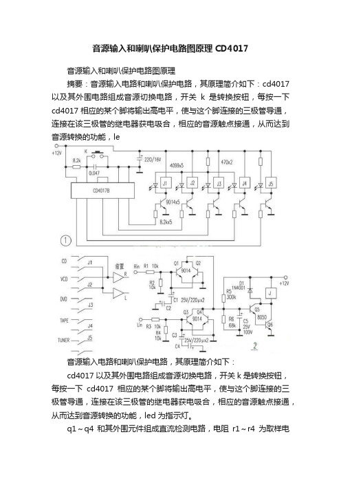
音源输入和喇叭保护电路图原理CD4017
音源输入和喇叭保护电路图原理
摘要:音源输入电路和喇叭保护电路,其原理简介如下:cd4017以及其外围电路组成音源切换电路,开关k是转换按钮,每按一下cd4017相应的某个脚将输出高电平,使与这个脚连接的三极管导通,连接在该三极管的继电器获电吸合,相应的音源触点接通,从而达到音源转换的功能,le
音源输入电路和喇叭保护电路,其原理简介如下:
cd4017以及其外围电路组成音源切换电路,开关k是转换按钮,每按一下cd4017相应的某个脚将输出高电平,使与这个脚连接的三极管导通,连接在该三极管的继电器获电吸合,相应的音源触点接通,从而达到音源转换的功能,led为指示灯。
q1~q4和其外围元件组成直流检测电路,电阻r1~r4为取样电
路,电容c1~c4可虑掉音频交流成分,lin和rin分别接功放的左右输出端。
当功放输出端有直流成分输出并达到一定幅度时,q1~q4中相应的三极管导通,从而使三极管q5基极变成低电位,q5、q6截止,继电器j触点释放,切断扬声器与电路的连接,喇叭得到保护。
电容c5起延时的作用,电路接通电源后电容c5通过电阻r5对其充电,三极管q5基极为低电平不导通,随着充电过程的完成,q5基极电平变高导通,继电器吸合,扬声器延时接通,避免功放电路刚接通电源时产生的噪音从扬声器里发出。
- 1、下载文档前请自行甄别文档内容的完整性,平台不提供额外的编辑、内容补充、找答案等附加服务。
- 2、"仅部分预览"的文档,不可在线预览部分如存在完整性等问题,可反馈申请退款(可完整预览的文档不适用该条件!)。
- 3、如文档侵犯您的权益,请联系客服反馈,我们会尽快为您处理(人工客服工作时间:9:00-18:30)。
CD4017引脚图,引脚功能及工作时序图
CD4017功能简述:
CD4017是5位Johnson计算器,具有10个译码输出端,CP,CR,INH输入端。
时钟输入端的斯密特触发器具有脉冲整形功能,对输入时钟脉冲上升和下降时间无限制。
INH为低电平时,计算器在时钟上升沿计数;反之,计数功能无效。
CR为高电平时,计数器清零。
Johnson计数器,提供了快速操作,2输入译码选通和无毛刺译码输出。
防锁选通,保证了正确的计数顺序。
译码输出一般为低电平,只有在对应时钟周期内保持高电平。
在每10个时钟输入周期CO信号完成一次进位,并用作多级计数链的下级脉动时钟。
CD4017引脚功能:
CD4017内部是除10的计数器及二进制对10进制译码电路。
CD4017有16支脚,除电源脚VDD及VSS 为电源接脚,输入电压范围为3–15V之外,其余接脚为:
A、频率输入脚:CLOCK(Pin14),为频率信号的输入脚。
B、数据输出脚:
a、Q1-Q9(Pin3,2,4,7,10,1,5,6,9,11),为*后的时进制输出接脚,被计数到的值,其输出为Hi,其余为Lo 电位。
b、CARRY OUT(Pin12),进位脚,当4017计数10个脉冲之后,CARRY OUT将输出一个脉波,代表产生进位,共串级计数器使用。
D、控制脚:
a、CLEAR(Pin15):清除脚或称复位(Reset)脚,当此脚为Hi时,会使CD4017的Q0为”1”,其余Q1-Q9为”0”。
b、CLOCK ENABLE(Pin13),时序允许脚,当此脚为低电位,CLOCK输入脉波在正缘时,会使CD4017计数,并改变Q1-Q9的输出状态。