MAX5160LEUA+T中文资料
电能计量元器件
本科毕设:不要求通信,只需要计算出用电器的电能,并在LCD上面进行显示,结合灯光控制来做。
硬件电路:ATmega16单片机,电流互感器,电压互感器,电能计量芯片,
电能计量芯片:电能计量芯片根据其内部的瞬时电压和瞬时电流计算瞬时功率,再输出脉冲驱动机械式计数器或者步进电机计算用电电量。
电能计量专用芯片:CS546OA,具有片内看门狗定时器与内部电源监视器;具有瞬时电流、瞬时电压、瞬时功率、电流有效值、电压有效值、功率有效值测量及电能计量功能;提供了外部复位引脚(这个地方可以重新进行计数);双向串行接口与内部寄存器阵列可以方便地与微处理器相连接;外部时钟最高频率可达20MHz;具有功率方向输出指示。
这些增加的功能更加便于与微控制器接口,并能方便地实现电压、电流、功率的测量和用电量累积等功能。
据此选择CS5460A作为电能计量芯片更能实现各种电参数的测量。
5160芯片手册
5160芯片手册1. 概述5160芯片是一款高性能的处理器芯片,专为计算机应用而设计。
本手册旨在提供对5160芯片的详细介绍和操作指南,以便用户充分利用其优秀的性能和功能。
2. 技术规格- 架构:x86- 主频:3.2 GHz- 核心数:4核- 线程数:8线程- 缓存容量:8 MB- 制造工艺:14nm- 功耗:65W- 支持技术:超线程技术、虚拟化技术、动态加速技术等3. 主要特点3.1 高性能5160芯片采用先进的架构和制造工艺,具备超强的性能表现,可以满足用户对于计算速度和响应能力的要求。
3.2 低功耗5160芯片的低功耗设计使其更加节能环保,同时也可以提升工作效率和降低使用成本。
3.3 多核心多线程5160芯片拥有4个独立的处理核心和8个线程,可以同时处理多个任务,提高系统的多任务处理能力。
3.4 先进技术支持5160芯片具备先进的技术支持,包括超线程技术、虚拟化技术和动态加速技术等,可以提供更好的用户体验和系统性能。
4. 功能描述4.1 超线程技术5160芯片支持超线程技术,可以将每个物理处理器核心模拟成两个逻辑核心,实现更高的并行处理能力。
4.2 虚拟化技术5160芯片内置虚拟化技术,可以将物理资源划分为多个逻辑部分,实现资源共享和提高系统利用率。
4.3 动态加速技术5160芯片的动态加速技术可以根据负载情况自动提升主频,以实现更好的性能和更快的响应速度。
4.4 安全保护5160芯片配备了多种安全保护功能,包括硬件加密引擎、访问控制和安全启动等,可以有效保护用户的数据安全。
5. 应用领域5160芯片广泛应用于各类计算机设备和系统,包括个人电脑、服务器、工作站等。
其卓越的性能和稳定性可以满足各种应用场景的需求。
6. 使用指南6.1 安装和连接5160芯片的安装和连接相对简单,用户只需根据设备的说明书进行正确操作即可。
6.2 驱动安装在使用5160芯片之前,用户需要安装相应的驱动程序,以确保硬件和系统的正常协同工作。
CS5160资料
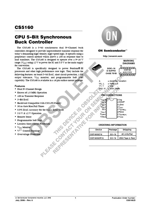
CS5160CPU 5−Bit Synchronous Buck ControllerThe CS5160 is a 5−bit synchronous dual N −Channel buck controllers designed to provide unprecedented transient response for today’s demanding high −density, high −speed logic. It operates using a proprietary control method which allows a 100 ns response time torange (V CC Features•Dual N −•••5−••••••••V CC •V 2™•*The maximum package power dissipation must be observed.MAXIMUM RATINGSPin Name Max Operating Voltage Max CurrentV CC116 V/−0.3 V100 mA DC/1.5 A peakV CC218 V/−0.3 V100 mA DC/1.5 A peakSS 6.0 V/−0.3 V−100 μACOMP 6.0 V/−0.3 V200 μAMAXIMUM RATINGS (continued)Max Operating VoltagePin Name Max CurrentV FB 6.0 V/−0.3 V−0.2 μAC OFF 6.0 V/−0.3 V−0.2 μAV FFB 6.0 V/−0.3 V−0.2 μAV ID0− V ID4 6.0 V/−0.3 V−50 μAV GATE(H)18 V/−0.3 V100 mA DC/1.5 A peakV GATE(L)16 V/−0.3 V100 mA DC/1.5 A peakLGnd0 V25 mAPGnd0 V100 mA DC/1.5 A peak ELECTRICAL CHARACTERISTICS (0°C < T A< +70°C; 0°C < T J < +85°C; 9.5V < V CC1 < 14V; 5.0V < V CC2< 16V; DACCode: V ID4=V ID2=V ID1=V ID0 =1; V ID3=0;CV GATE(L)and CV GATE(H) = 1.0nF; C OFF = 330 pF; C SS = 0.1 μF, unless otherwise specified.) Characteristic Test Conditions Min Typ Max Unit Error AmplifierV FB Bias Current V FB = 0 V−0.3 1.0μA Open Loop Gain 1.25 V < V COMP , 4.0 V; C COMP = 0.1 μF;−80−dBNote 2Unity Gain Bandwidth C COMP= 0.1 μF; Note 2−50−kHz COMP SINK Current V COMP = 1.5 V; V FB = 3.0 V; V SS > 2.0 V3060120μA COMP SOURCE Current V COMP = 1.2 V; V FB = 2.7 V; V SS = 5.0 V153060μA COMP CLAMP Current V COMP = 0 V; V FB = 2.7 V0.4 1.0 1.6mA COMP High Voltage V FB = 2.7 V; V SS = 5.0 V 4.0 4.3 5.0V COMP Low Voltage V FB = 3.0 V− 1.00 1.15V−70−dB PSRR8.0 V < V CC1 < 14 V @ 1.0 kHz;C COMP = 0.1 μF; Note 2Transconductance−−33−mmho V CC1 MonitorStart Threshold Output switching8.608.959.30V Stop Threshold Output not switching8.458.809.15V Hysteresis Start−Stop−150−mV Soft Start (SS)Charge Time− 1.6 3.3 5.0ms Pulse Period−25100200ms Duty Cycle(Charge Time /Pulse Period) × 100 1.0 3.3 6.0% COMP Clamp Voltage V FB = 0 V; V SS = 00.500.95 1.10V V FFB SS Fault Disable V GATE(H) = Low; V GATE(L) = Low0.9 1.0 1.1V High Threshold−− 2.5 3.0V 2.Guaranteed by design, not 100% tested in production.ELECTRICAL CHARACTERISTICS (continued) (0°C < T A< +70°C; 0°C < T J < +85°C; 9.5V < V CC1 < 14V; 5.0V < V CC2< 16V; DAC Code: V ID4=V ID2=V ID1=V ID0 =1; V ID3=0;CV GATE(L)and CV GATE(H) = 1.0nF; C OFF = 330 pF; C SS = 0.1 μF, unless otherwise specified.) Characteristic UnitMaxTypMinTest ConditionsPWM ComparatorTransient Response V FFB = 0 to 5.0 V to V GATE(H) = 9.0 V to 1.0 V;V CC1 = V CC2 = 12 V−100125ns V FFB Bias Current V FFB = 0 V−0.3−μA DACInput Threshold V ID0,V ID1, V ID2, V ID3, V ID4 1.00 1.25 2.40V Input Pull Up Resistance V ID0,V ID1, V ID2, V ID3, V ID42550110kΩPull Up Voltage− 4.85 5.00 5.15VAccuracy (all codes except 11111, 10110, 10101, 10100, 10011, 10010, 10001, 10000, and 01111)Measure V FB = COMP,CS5160: 25°C ≤ T J≤ 85°C−− 1.0%V ID4V ID3V ID2V ID1V ID001111− 1.2896 1.3000 1.3104V 01110− 1.3365 1.3500 1.3635V 01101− 1.3860 1.4000 1.4140V 01100− 1.4355 1.4500 1.4645V 01011− 1.4850 1.5000 1.5150V 01010− 1.5345 1.5500 1.5655V 01001− 1.5840 1.6000 1.6160V 01000− 1.6335 1.6500 1.6665V 00111− 1.6830 1.7000 1.7170V 00110− 1.7325 1.7500 1.7675V 00101− 1.7820 1.8000 1.8180V 00100− 1.8315 1.8500 1.8685V 00011− 1.8810 1.9000 1.9190V 00010− 1.9305 1.9500 1.9695V 00001− 1.9800 2.0000 2.0200V 00000− 2.0295 2.0500 2.0705V 11111− 1.2191 1.2440 1.2689V 11110− 2.0790 2.1000 2.1210V 11101− 2.1780 2.2000 2.2220V 11100− 2.2770 2.3000 2.3230V 11011− 2.3760 2.4000 2.4240V 11010− 2.4750 2.5000 2.5250V 11001− 2.5740 2.6000 2.6260V 11000− 2.6730 2.7000 2.7270V 10111− 2.7720 2.8000 2.8280V 10110− 2.8420 2.9000 2.9580V 10101− 2.9400 3.0000 3.0600V 10100− 3.0380 3.1000 3.1620VELECTRICAL CHARACTERISTICS (continued) (0°C < T A< +70°C; 0°C < T J < +85°C; 9.5V < V CC1 < 14V; 5.0V < V CC2< 16V; DAC Code: V ID4=V ID2=V ID1=V ID0 =1; V ID3=0;CV GATE(L)and CV GATE(H) = 1.0nF; C OFF = 330 pF; C SS = 0.1 μF, unless otherwise specified.)TypTest ConditionsMinCharacteristic UnitMaxDAC10011− 3.1360 3.2000 3.2640V 10010− 3.2340 3.3000 3.3660V 10001− 3.3320 3.4000 3.4680V 10000− 3.4300 3.5000 3.5700V V GATE(H) and V GATE(L)Out SOURCE Sat at 100 mA Measure V CC1− V GATE(L); V CC2− V GATE(H)− 1.2 2.0V Out SINK Sat at 100 mA Measure V GATE(H)− V PGnd; V GATE(L)− V PGnd− 1.0 1.5V−3050ns Out Rise Time 1.0 V < V GATE(H) < 9.0 V; 1.0 V < V GATE(L)< 9.0 V; V CC1 = V CC2 = 12 VOut Fall Time9.0 V < V GATE(H) > 1.0 V; 9.0 V > V GATE(L)−3050ns> 1.0 V; V CC1 = V CC2 = 12 V457095ns Delay V GATE(H)to V GATE(L)V GATE(H)falling to 1.0 V; V CC1 = V CC2 = 8.0 VCV GATE(H) = 3.3 nF; V GATE(L) rising to 1.0 VDelay V GATE(L)to V GATE(H)V GATE(L) falling to 1.0 V; V CC1 = V CC2 = 8.0 V457095nsCV GATE(H) = 3.3 nF; V GATE(H) rising to 1.0 VV GATE(H),V GATE(L) Resistance Resistor to LGnd. Note 32050100kΩ−600800mV V GATE(H),V GATE(L) Schottky LGnd to V GATE(H) @ 10 mA;LGnd to V GATE(L) @ 10 mASupply CurrentI CC1 No Switching−−9.514.5mA I CC2 No Switching−− 2.0 3.5mA Operating I CC1V FB = COMP = V FFB−9.014mA Operating I CC2V FB = COMP = V FFB− 2.5 5.5mA C OFFNormal Charge Time V FFB = 1.5 V; V SS = 5.0 V 1.0 1.6 2.2μs Discharge Current C OFF to 5.0 V; V FB > 1.0 V 5.0−−mA Time Out TimerTime Out Time V FB = V COMP; V FFB = 2.0 V;103065μsRecord V GATE(H) Pulse High DurationFault Mode Duty Cycle V FFB = 0V355070% 3.Guaranteed by design, not 100% tested in production.PACKAGE PIN DESCRIPTIONPACKAGE PIN #PIN SYMBOL FUNCTION16 Lead SO Narrow1, 2, 3, 4, 6V ID0−V ID4Voltage ID DAC input pins. These pins are internally pulledup to 5.0 V providing logic ones if left open. V ID4 selects theDAC range. When V ID4 is High (logic one), the DAC rangeis 2.10 V to 3.50 V with 100 mV increments. When V ID4 isLow (logic zero), the DAC range is 1.30 V to 2.05 V with50 mV increments. V ID0− V ID4 select the desired DAC out-put voltage. Leaving all 5 DAC input pins open results in aDAC output voltage of 1.2440 V, allowing for adjustableoutput voltage, using a traditional resistor divider.5SS Soft Start Pin. A capacitor from this pin to LGnd in conjunc-tion with internal 60 μA current source provides Soft Startfunction for the controller. This pin disables fault detect func-tion during Soft Start. When a fault is detected, the Soft Startcapacitor is slowly discharged by internal 2.0 μA currentsource setting the time out before trying to restart the IC.Charge/discharge current ratio of 30 sets the duty cycle forthe IC when the regulator output is shorted.7C OFF A capacitor from this pin to ground sets the time duration forthe on board one shot, which is used for the constant off timearchitecture.8V FFB Fast feedback connection to the PWM comparator. This pinis connected to the regulator output. The inner feedback loopterminates on time.9V CC2Boosted power for the high side gate driver.10V GATE(H)High FET driver pin capable of 1.5 A peak switching current.Internal circuit prevents V GATE(H) and V GATE(L) from being inhigh state simultaneously.11PGnd High current ground for the IC. The MOSFET drivers arereferenced to this pin. Input capacitor ground and the sourceof lower FET should be tied to this pin.12V GATE(L)Low FET driver pin capable of 1.5 A peak switching current.13V CC1Input power for the IC and low side gate driver.14LGnd Signal ground for the IC. All control circuits are referenced tothis pin.15COMP Error amplifier compensation pin. A capacitor to groundshould be provided externally to compensate the amplifier.16V FB Error amplifier DC feedback input. This is the master voltagefeedback which sets the output voltage. This pin can be con-nected directly to the output or a remote sense trace.VVVVVVVV2Figure 3. V2 Control DiagramThe V2 control method is illustrated in Figure 3. The output voltage is used to generate both the error signal and the ramp signal. Since the ramp signal is simply the output voltage, it is affected by any change in the output regardless of the origin of that change. The ramp signal also contains the DC portion of the output voltage, which allows the control circuit to drive the main switch to 0% or 100% duty cycle as required.A change in line voltage changes the current ramp in the inductor, affecting the ramp signal, which causes the V2 control scheme to compensate the duty cycle. Since the change in inductor current modifies the ramp signal, as in current mode control, the V2 control scheme has the same advantages in line transient response.A change in load current will have an affect on the output voltage, altering the ramp signal. A load step immediately changes the state of the comparator output, which controls the main switch. Load transient response is determined only by the comparator response time and the transition speed of the main switch. The reaction time to an output load step has no relation to the crossover frequency of the error signal loop, as in traditional control methods.The error signal loop can have a low crossover frequency, since transient response is handled by the ramp signal loop. The main purpose of this ‘slow’ feedback loop is to provide DC accuracy. Noise immunity is significantly improved, since the error amplifier bandwidth can be rolled off at a low frequency. Enhanced noise immunity improves remote sensing of the output voltage, since the noise associated with long feedback traces can be effectively filtered.Line and load regulation are drastically improved because there are two independent voltage loops. A voltage mode controller relies on a change in the error signal to compensate for a deviation in either line or load voltage. This change in the error signal causes the output voltage to change corresponding to the gain of the error amplifier, which is normally specified as line and load regulation. A current mode controller maintains fixed error signal under deviation in the line voltage, since the slope of the ramp signal changes, but still relies on a change in the error signal for a deviation in load. The V2 method of control maintains a fixed error signal for both line and load variation, since the ramp signal is affected by both line and load.Constant Off TimeTo maximize transient response, the CS5160 uses a constant off time method to control the rate of output pulses. During normal operation, the off time of the high side switch is terminated after a fixed period, set by the C OFF capacitor. To maintain regulation, the V2 control loop varies switch on time. The PWM comparator monitors the output voltage ramp, and terminates the switch on time.Constant off time provides a number of advantages. Switch duty cycle can be adjusted from 0 to 100% on a pulse by pulse basis when responding to transient conditions. Both 0% and 100% duty cycle operation can be maintained for extended periods of time in response to load or line transients. PWM slope compensation to avoid sub−harmonic oscillations at high duty cycles is avoided. Switch on time is limited by an internal 30 μs timer, minimizing stress to the power components. Programmable OutputThe CS5160 is designed to provide two methods for programming the output voltage of the power supply. A five bit on board digital to analog converter (DAC) is used to program the output voltage within two different ranges. The first range is 2.10 V to 3.50 V in 100 mV steps, the second is 1.30 V to 2.05 V in 50 mV steps, depending on the digital input code. If all five bits are left open, the CS5160 enters adjust mode. In adjust mode, the designer can choose any output voltage by using resistor divider feedback to the V FB and V FFB pins, as in traditional controllers.Start UpUntil the voltage on the V CC1 supply pin exceeds the 9.05 V monitor threshold, the Soft Start and gate pins are held low. The FAULT latch is reset (no Fault condition). The output of the error amplifier (COMP) is pulled up to 1.0 V by the comparator clamp. When the V CC1 pin exceeds the monitor threshold, the GA TE(H) output is activated, and the Soft Start capacitor begins charging. The GATE(H) output will remain on, enabling the NFET switch, until terminated by either the PWM comparator, or the maximum on time timer.If the maximum on time is exceeded before the regulator output voltage achieves the 1.0 V level, the pulse is terminated. The GA TE(H) pin drives low, and the GATE(L) pin drives high for the duration of the extended off time. This time is set by the time out timer and is approximately equal to the maximum on time, resulting in a 50% duty cycle. The GATE(L) pin will then drive low, the GATE(H) pin will drive high, and the cycle repeats.When regulator output voltage achieves the 1.0 V level present at the COMP pin, regulation has been achieved and normal off time will ensue. The PWM comparator terminates the switch on time, with off time set by the C OFF capacitor. The V2 control loop will adjust switch duty cycle as required to ensure the regulator output voltage tracks the output of the error amplifier.The Soft Start and COMP capacitors will charge to their final levels, providing a controlled turn on of the regulator output. Regulator turn on time is determined by the COMP capacitor charging to its final value. Its voltage is limited bythe Soft Start COMP clamp and the voltage on the Soft Start pin (see Figures 4 and 5).Figure 4. CS5160 Startup in Response to Increasing 12 V and 5.0 V Input Voltages. Extended Off Time is Followed by Normal Off Time Operation when Output Voltage Achieves Regulation to the Error AmplifierOutputM 250 μsTrace 3− 12 V Input (VCC1 and VCC2) (5.0 V/div.)Trace 1− Regulator Output Voltage (1.0 V/div.)Trace 4− 5.0 V Input (1.0 V/div.)Trace 2− Inductor Switching Node (2.0 V/div.)Figure 5. CS5160 Startup WaveformsM 2.50 msTrace 3− COMP PIn (error amplifier output) (1.0 V/div.)Trace 1− Regulator Output Voltage (1.0 V/div.)Trace 4− Soft Start Pin (2.0 V/div.)If the input voltage rises quickly, or the regulator output is enabled externally, output voltage will increase to the level set by the error amplifier output more rapidly, usuallywithin a couple of cycles (see Figure 6).Figure 6. CS5160 Enable Startup Waveforms M 10.0 μsTrace 1− Regulator Output Voltage (5.0 V/div.)Trace 2− Inductor Switching Node (5.0 V/div.)Normal OperationDuring normal operation, switch off time is constant and set by the C OFF capacitor. Switch on time is adjusted by the V 2 control loop to maintain regulation. This results in changes in regulator switching frequency, duty cycle, and output ripple in response to changes in load and line. Output voltage ripple will be determined by inductor ripple current working into the ESR of the output capacitors (see Figures 7 and 8).Figure 7. CS5160 Peak −to −Peak Ripple on V OUT = 2.8 V,I OUT= 0.5 A (Light Load)M 1.00 μsTrace 1− Regulator Output Voltage (10 mV/div.)Trace 2− Inductor Switching Node (5.0 V/div.)Voltage Response to a 12 A Load Pulse100 μs/div.10 μs/div.10 μs/div.(V FFB < 1.0 V), the V FFB low comparator sets the FAULTlatch. This causes the top MOSFET to shut off,disconnecting the regulator from it’s input voltage. The Soft Start capacitor is then slowly discharged by a 2.0 μA current source until it reaches it’s lower 0.7 V threshold. The regulator will then attempt to restart normally, operating in it’s extended off time mode with a 50% duty cycle, while the Soft Start capacitor is charged with a 60 μA charge current.If the short circuit condition persists, the regulator output will not achieve the 1.0 V low V FFB comparator threshold before the Soft Start capacitor is charged to it’s upper 2.5 V threshold. If this happens the cycle will repeat itself until the short is removed. The Soft Start charge/discharge current ratio sets the duty cycle for the pulses (2.0 μA/60 μA = 3.3%), while actual duty cycle is half that due to the extended off time mode (1.65%).This protection feature results in less stress to the regulator components, input power supply, and PC board traces than occurs with constant current limit protection (see Figures 12 and 13).If the short circuit condition is removed, output voltage will rise above the 1.0 V level, preventing the FAULT latch from being set, allowing normal operation to resume.Figure 12. CS5160 Hiccup Mode Short Circuit Protection. Gate Pulses are Delivered While the Soft Start Capacitor Charges, and Cease During DischargeM 25.0 msTrace 3− Soft Start Timing Capacitor (1.0 V/div.)Trace 4− 5.0 V Supply Voltage (2.0 V/div.)Trace 2− Inductor Switching Node (2.0 V/div.)Figure 13. CS5160 Startup with RegulatorOutput ShortedM 50.0 μsTrace 4− 5.0 V from PC Power Supply (2.0 V/div.)Trace 2− Inductor Switching Node (2.0 V/div.)Overvoltage ProtectionOvervoltage protection (OVP) is provided as result of the normal operation of the V 2 control topology and requires no additional external components. The control loop responds to an overvoltage condition within 100 ns, causing the top MOSFET to shut off, disconnecting the regulator from it’s input voltage. The bottom MOSFET is then activated,resulting in a “crowbar” action to clamp the output voltage and prevent damage to the load (see Figures 14 and 15). The regulator will remain in this state until the overvoltage condition ceases or the input voltage is pulled low. The bottom FET and board trace must be properly designed to implement the OVP function.Figure 14. CS5160 OVP Response to an Input −to −Output Short Circuit by Immediately Providing 0% Duty Cycle, Crow −Barring the InputVoltage to GroundM 10.0 μsTrace 1− Regulator Output Voltage (1.0 V/div.)Trace 2− Inductor Switching Node 5.0 V/div.)Trace 4− 5.0 V from PC Power Supply (5.0 V/div.)An optional Power Good signal can be generated through the use of four additional external components (see Figure 17). The threshold voltage of the Power Good signal can be adjusted per the following equation:V Power Good+(R1)R2)0.65VR2This circuit provides an open collector output that drives the Power Good output to ground for regulator voltages less than V Power Good.Figure 17. Implementing Power Goodwith the CS5160Figure 18. CS5160 During Power Up. PowerGood Signal is Activated when OutputVoltage Reaches 1.70 VM 2.50 msTrace 4− 5.0 V Input (2.0 V/div.)Trace 3 − 12 V Input (V CC1) and (V CC2) (10 V/div.)Trace 1− Regulator Output Voltage (1.0V/div.)Trace 2− Power Good Signal (2.0V/div.)−time.Adding slope compensation to the control loop, avoids erratic operation of the PWM circuit, particularly at lower duty cycles and higher frequencies, where there is not enough ramp signal, and provides a more stable switchpoint. The scheme that prevents that switching noise prematurely triggers the PWM circuit consists of adding a positive voltage slope to the output of the Error Amplifier (COMP pin) during an off−time cycle.The circuit that implements this function is shown in Figure 19.following gate drive is provided;V GATE(H)+12V*5.0V+7.0V,V GATE(L)+12V (see Figure 20.)Figure 20. CS5160 Gate Drive Waveforms DepictingRail to Rail SwingM 1.00 μsMath 1 = V GATE(H)− 5.0 V INTrace 3 = V GATE(H) (10 V/div.)Trace 4 = V GATE(L) (10V/div.)Trace 2= Inductor Switching Nodes (5.0V/div.)The most important aspect of MOSFET performance isPeriod+1switching frequencySchottky Diode for Synchronous MOSFETA Schottky diode may be placed in parallel with the synchronous MOSFET to conduct the inductor current upon turn off of the switching MOSFET to improve efficiency.For a design operating at 200 kHz or so, the low non −overlap time combined with Schottky forward recovery time may make the benefits of this device not worth the additional expense (see Figure 8, channel 2). The power dissipation in the synchronous MOSFET due to body diode conduction can be estimated by the following equation:Power +V BD I LOAD conduction time switching frequencyWhere VFigure 8;Power +load.Thermal A heatsink may be added to TO −220 components to reduce their thermal impedance. A number of PC board layout techniques such as thermal vias and additional copper foil area can be used to improve the power handling capability of surface mount components.EMI ManagementAs a consequence of large currents being turned on and off at high frequency, switching regulators generate noise as a consequence of their normal operation. When designing for compliance with EMI/EMC regulations, additional components may be added to reduce noise emissions. TheseLayout Guidelines1.2.3.4.5.6.7.V To the negative terminal V FFBADDITIONAL APPLICATION DIAGRAMS8.0 Figure 25. Pentium®III Converter with Slope Compensation and Adaptive Voltage PositioningPACKAGE DIMENSIONSSO −16D SUFFIX CASE 751B −05ISSUE Jand are trademarks of Semiconductor Components Industries, LLC (SCILLC). SCILLC reserves the right to make changes without further notice to any products herein. SCILLC makes no warranty, representation or guarantee regarding the suitability of its products for any particular PUBLICATION ORDERING INFORMATIONJAPAN : ON Semiconductor, Japan Customer Focus Center4−32−1 Nishi −Gotanda, Shinagawa −ku, Tokyo, Japan 141−0031Phone : 81−3−5740−2700Email : r14525@Literature Fulfillment :Literature Distribution Center for ON Semiconductor P.O. Box 5163, Denver, Colorado 80217 USAPhone : 303−675−2175 or 800−344−3860 Toll Free USA/Canada。
lm5160 FLY-BUCK
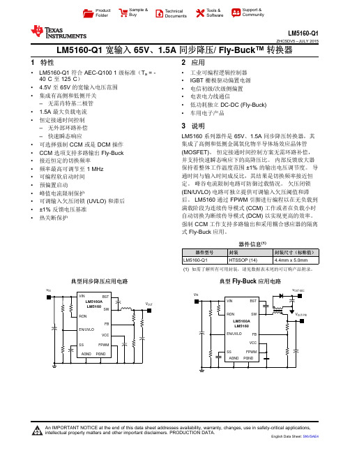
VOUT-SECProductFolderSample &BuyTechnicalDocumentsTools &SoftwareSupport &CommunityLM5160-Q1ZHCSDV5–JULY2015 LM5160-Q1宽输入65V、1.5A同步降压/Fly-Buck™转换器1特性2应用•LM5160-Q1符合AEC-Q1001级标准(T a=-•工业可编程逻辑控制器40°C至125°C)•IGBT栅极驱动偏置电源• 4.5V至65V的宽输入电压范围•电信初级/次级侧偏置•集成有高侧和低侧开关•电表电力线通信–无需肖特基二极管•低功耗独立DC-DC(Fly-Buck)• 1.5A最大负载电流•车用电子产品•恒定接通时间控制3说明–无外部环路补偿LM5160系列器件是65V、1.5A同步降压转换器,其–快速瞬态响应集成了高侧和低侧金属氧化物半导体场效应晶体管•可选择强制CCM或是DCM操作(MOSFET)。
恒定接通时间控制方案无需环路补偿,•CCM选项支持多路输出Fly-Buck并支持快速瞬态响应下的高降压比。
内部反馈放大器•接近恒定的切换频率保持着整体工作温度范围±1%的输出电压调节度。
导•频率最高可调节至1MHz通时间与输入时间成反比,其结果是切换频率接近恒•可编程软启动时间定。
峰谷电流限制电路可防御过载情况。
欠压闭锁•预偏置启动(EN/UVLO)电路可独立提供可调输入欠压阈值和滞•峰值电流限制保护后。
LM5160通过FPWM引脚进行编程以在无负载到•可调输入欠压闭锁(UVLO)和滞后满载阶段为连续传导模式(CCM)工作或者在负载小时•±1%反馈电压基准自动切换为断续传导模式(DCM)以实现更高的效率。
•热关断保护强制CCM工作支持多路输出和采用耦合感应器的隔离式Fly-Buck应用。
器件信息(1)器件型号封装封装尺寸(标称值)LM5160-Q1HTSSOP(14) 4.4mm x5.0mm(1)如需了解所有可用封装,请见数据表末尾的可订购产品附录。
MAX5161中文资料
RW CW
MAX516_NE_ _
400 1700
Ω
10
pF
150
200
250
End-to-End Resistance
HL
MAX516_ME_ _
75
100
125
kΩ
MAX516_LE_ _
37.5
50
62.5
DIGITAL INPUTS
Input High Voltage
VIH
Input Low Voltage
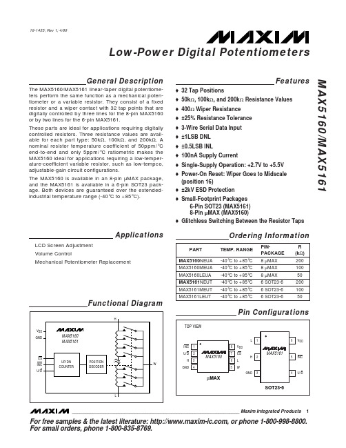
(position 16) o ±2kV ESD Protection o Small-Footprint Packages
6-Pin SOT23 (MAX5161) 8-Pin µMAX (MAX5160) o Glitchless Switching Between the Resistor Taps
Applications
LCD Screen Adjustment Volume Control Mechanical Potentiometer Replacement
Functional Diagram
H
VDD
GND
MAX5160
MAX5161
CS
INC
UP/DN COUNTER
POSITION DECODER
Stresses beyond those listed under “Absolute Maximum Ratings” may cause permanent damage to the device. These are stress ratings only, and functional operation of the device at these or any other conditions beyond those indicated in the operational sections of the specifications is not implied. Exposure to absolute maximum rating conditions for extended periods may affect device reliability.
AD5160官方中文

功能框图
VDD A
B
GND
图1
应用
在新设计中代替机械电位计 压力、温度、位置、化学和光学传感器调节 RF放大器偏置 汽车电子设备调节 增益控制和失调电压调整
W 1 VDD 2 60 7 B
6 CS TOP VIEW CLK 4 (Not to Scale) 5 SDI
图2
概述
AD5160是一款适合256位调整应用的2.9 mm x 3 mm紧凑型 封装解决方案,可实现与机械电位计 或可变电阻器相同 的电子调整功能,而且具有增强的分辨率、固态可靠性和 出色的低温度系数性能。
1
游标设置可通过SPI兼容型数字接口控制。游标与固定电 阻任一端点之间的电阻值,随传输至RDAC锁存器中的数 字码呈线性变化。 该器件采用2.7 V至5.5 V电源供电,功耗小于5 µA,适合电 池供电的便携式应用。
ADI中文版数据手册是英文版数据手册的译文,敬请谅解翻译中可能存在的语言组织或翻译错误,ADI不对翻译中存在的差异或由此产生的错误负责。如需确认任何词语的准确性,请参考ADI提供 的最新英文版数据手册。
AD5160
目录
产品特性 ........................................................................................... 1 应用.................................................................................................... 1 功能框图 ........................................................................................... 1 引脚配置 ........................................................................................... 1 概述.................................................................................................... 1 修订历史 ........................................................................................... 2 技术规格 ........................................................................................... 3 电气特性——5 k 版本 ............................................................ 3 10 k 、50 k 、100 k 版本.................................................... 4 时序特性——所有版本 ............................................................ 5 绝对最大额定值.............................................................................. 6 ESD警告....................................................................................... 6 引脚配置和功能描述 ..................................................................... 7 典型工作特性 .................................................................................. 8 测试电路 ......................................................................................... 12 SPI接口............................................................................................ 13 工作原理 ......................................................................................... 14 可变电阻器编程....................................................................... 14 电位计分压器编程 .................................................................. 15 SPI兼容型三线式串行总线 ................................................... 15 ESD保护..................................................................................... 15 上电时序.................................................................................... 15 布局布线和电源旁路.............................................................. 15 外形尺寸 ......................................................................................... 16 订购指南.................................................................................... 16
MX5068的使用说明书
MX5068的使用说明书
控制形式:全自动
售后服务:一年保修,免费咨询
是否进口:否
公司行业:木工机械
产地:江苏东台
包装:完好
供货方式:直销
规格:1470乘920乘1700mm
经营模式:直销
适用范围:通用
种类:气动镂铣机
用途:通用
功率:4kw
加工定制:是
型号:MX5068
产品特点:镂铣机使用比较灵活,可以根据我们所需要的形状制作出合适的模具,安装合适的型刀就可以进行我们的要求加工。
木工镂铣机利用模板可以进行木制品零部件的刨光、倒角、仿形(仿形开圆孔、椭圆孔、不规则孔及仿形铣简单浮雕)等。
铣床是通过铣刀旋转对工件进行铣削加工的机床。
铣床除能铣削平面、沟槽、轮齿、螺纹和花键轴外,还能加工比较复杂的型面,效率较刨床高,在机械制
造和修理部门得到广泛应用。
其中数控铣才能加工复杂零件.。
MAX490ESA+T中文资料

For pricing, delivery, and ordering information,please contact Maxim/Dallas Direct!at 1-888-629-4642, or visit Maxim’s website at .General DescriptionThe MAX481, MAX483, MAX485, MAX487–MAX491, and MAX1487 are low-power transceivers for RS-485 and RS-422 communication. Each part contains one driver and one receiver. The MAX483, MAX487, MAX488, and MAX489feature reduced slew-rate drivers that minimize EMI and reduce reflections caused by improperly terminated cables,thus allowing error-free data transmission up to 250kbps.The driver slew rates of the MAX481, MAX485, MAX490,MAX491, and MAX1487 are not limited, allowing them to transmit up to 2.5Mbps.These transceivers draw between 120µA and 500µA of supply current when unloaded or fully loaded with disabled drivers. Additionally, the MAX481, MAX483, and MAX487have a low-current shutdown mode in which they consume only 0.1µA. All parts operate from a single 5V supply.Drivers are short-circuit current limited and are protected against excessive power dissipation by thermal shutdown circuitry that places the driver outputs into a high-imped-ance state. The receiver input has a fail-safe feature that guarantees a logic-high output if the input is open circuit.The MAX487 and MAX1487 feature quarter-unit-load receiver input impedance, allowing up to 128 MAX487/MAX1487 transceivers on the bus. Full-duplex communi-cations are obtained using the MAX488–MAX491, while the MAX481, MAX483, MAX485, MAX487, and MAX1487are designed for half-duplex applications.________________________ApplicationsLow-Power RS-485 Transceivers Low-Power RS-422 Transceivers Level TranslatorsTransceivers for EMI-Sensitive Applications Industrial-Control Local Area Networks__Next Generation Device Features♦For Fault-Tolerant ApplicationsMAX3430: ±80V Fault-Protected, Fail-Safe, 1/4Unit Load, +3.3V, RS-485 TransceiverMAX3440E–MAX3444E: ±15kV ESD-Protected,±60V Fault-Protected, 10Mbps, Fail-Safe, RS-485/J1708 Transceivers♦For Space-Constrained ApplicationsMAX3460–MAX3464: +5V, Fail-Safe, 20Mbps,Profibus RS-485/RS-422 TransceiversMAX3362: +3.3V, High-Speed, RS-485/RS-422Transceiver in a SOT23 PackageMAX3280E–MAX3284E: ±15kV ESD-Protected,52Mbps, +3V to +5.5V, SOT23, RS-485/RS-422,True Fail-Safe ReceiversMAX3293/MAX3294/MAX3295: 20Mbps, +3.3V,SOT23, RS-855/RS-422 Transmitters ♦For Multiple Transceiver ApplicationsMAX3030E–MAX3033E: ±15kV ESD-Protected,+3.3V, Quad RS-422 Transmitters ♦For Fail-Safe ApplicationsMAX3080–MAX3089: Fail-Safe, High-Speed (10Mbps), Slew-Rate-Limited RS-485/RS-422Transceivers♦For Low-Voltage ApplicationsMAX3483E/MAX3485E/MAX3486E/MAX3488E/MAX3490E/MAX3491E: +3.3V Powered, ±15kV ESD-Protected, 12Mbps, Slew-Rate-Limited,True RS-485/RS-422 TransceiversMAX481/MAX483/MAX485/MAX487–MAX491/MAX1487Low-Power, Slew-Rate-Limited RS-485/RS-422 Transceivers______________________________________________________________Selection Table19-0122; Rev 8; 10/03Ordering Information appears at end of data sheet.M A X 481/M A X 483/M A X 485/M A X 487–M A X 491/M A X 1487Low-Power, Slew-Rate-Limited RS-485/RS-422 Transceivers 2_______________________________________________________________________________________ABSOLUTE MAXIMUM RATINGSSupply Voltage (V CC ).............................................................12V Control Input Voltage (RE , DE)...................-0.5V to (V CC + 0.5V)Driver Input Voltage (DI).............................-0.5V to (V CC + 0.5V)Driver Output Voltage (A, B)...................................-8V to +12.5V Receiver Input Voltage (A, B).................................-8V to +12.5V Receiver Output Voltage (RO).....................-0.5V to (V CC +0.5V)Continuous Power Dissipation (T A = +70°C)8-Pin Plastic DIP (derate 9.09mW/°C above +70°C)....727mW 14-Pin Plastic DIP (derate 10.00mW/°C above +70°C)..800mW 8-Pin SO (derate 5.88mW/°C above +70°C).................471mW14-Pin SO (derate 8.33mW/°C above +70°C)...............667mW 8-Pin µMAX (derate 4.1mW/°C above +70°C)..............830mW 8-Pin CERDIP (derate 8.00mW/°C above +70°C).........640mW 14-Pin CERDIP (derate 9.09mW/°C above +70°C).......727mW Operating Temperature RangesMAX4_ _C_ _/MAX1487C_ A...............................0°C to +70°C MAX4__E_ _/MAX1487E_ A.............................-40°C to +85°C MAX4__MJ_/MAX1487MJA...........................-55°C to +125°C Storage Temperature Range.............................-65°C to +160°C Lead Temperature (soldering, 10sec).............................+300°CDC ELECTRICAL CHARACTERISTICS(V CC = 5V ±5%, T A = T MIN to T MAX , unless otherwise noted.) (Notes 1, 2)Stresses beyond those listed under “Absolute Maximum Ratings” may cause permanent damage to the device. These are stress ratings only, and functional operation of the device at these or any other conditions beyond those indicated in the operational sections of the specifications is not implied. Exposure to absolute maximum rating conditions for extended periods may affect device reliability.V V IN = -7VV IN = 12V V IN = -7V V IN = 12V Input Current (A, B)I IN2V TH k Ω48-7V ≤V CM ≤12V, MAX487/MAX1487R INReceiver Input Resistance -7V ≤V CM ≤12V, all devices except MAX487/MAX1487R = 27Ω(RS-485), Figure 40.4V ≤V O ≤2.4VR = 50Ω(RS-422)I O = 4mA, V ID = -200mV I O = -4mA, V ID = 200mV V CM = 0V-7V ≤V CM ≤12V DE, DI, RE DE, DI, RE MAX487/MAX1487,DE = 0V, V CC = 0V or 5.25VDE, DI, RE R = 27Ωor 50Ω, Figure 4R = 27Ωor 50Ω, Figure 4R = 27Ωor 50Ω, Figure 4DE = 0V;V CC = 0V or 5.25V,all devices except MAX487/MAX1487CONDITIONSk Ω12µA ±1I OZRThree-State (high impedance)Output Current at ReceiverV 0.4V OL Receiver Output Low Voltage 3.5V OH Receiver Output High Voltage mV 70∆V TH Receiver Input Hysteresis V -0.20.2Receiver Differential Threshold Voltage-0.2mA 0.25mA-0.81.01.55V OD2Differential Driver Output (with load)V 2V 5V OD1Differential Driver Output (no load)µA±2I IN1Input CurrentV 0.8V IL Input Low Voltage V 2.0V IH Input High Voltage V 0.2∆V OD Change in Magnitude of Driver Common-Mode Output Voltage for Complementary Output States V 0.2∆V OD Change in Magnitude of Driver Differential Output Voltage for Complementary Output States V 3V OC Driver Common-Mode Output VoltageUNITS MINTYPMAX SYMBOL PARAMETERMAX481/MAX483/MAX485/MAX487–MAX491/MAX1487Low-Power, Slew-Rate-Limited RS-485/RS-422 Transceivers_______________________________________________________________________________________3SWITCHING CHARACTERISTICS—MAX481/MAX485, MAX490/MAX491, MAX1487(V CC = 5V ±5%, T A = T MIN to T MAX , unless otherwise noted.) (Notes 1, 2)DC ELECTRICAL CHARACTERISTICS (continued)(V CC = 5V ±5%, T A = T MIN to T MAX , unless otherwise noted.) (Notes 1, 2)ns 103060t PHLDriver Rise or Fall Time Figures 6 and 8, R DIFF = 54Ω, C L1= C L2= 100pF ns MAX490M, MAX491M MAX490C/E, MAX491C/E2090150MAX481, MAX485, MAX1487MAX490M, MAX491MMAX490C/E, MAX491C/E MAX481, MAX485, MAX1487Figures 6 and 8, R DIFF = 54Ω,C L1= C L2= 100pF MAX481 (Note 5)Figures 5 and 11, C RL = 15pF, S2 closedFigures 5 and 11, C RL = 15pF, S1 closed Figures 5 and 11, C RL = 15pF, S2 closed Figures 5 and 11, C RL = 15pF, S1 closed Figures 6 and 10, R DIFF = 54Ω,C L1= C L2= 100pFFigures 6 and 8,R DIFF = 54Ω,C L1= C L2= 100pF Figures 6 and 10,R DIFF = 54Ω,C L1= C L2= 100pF CONDITIONS ns 510t SKEW ns50200600t SHDNTime to ShutdownMbps 2.5f MAX Maximum Data Rate ns 2050t HZ Receiver Disable Time from High ns 103060t PLH 2050t LZ Receiver Disable Time from Low ns 2050t ZH Driver Input to Output Receiver Enable to Output High ns 2050t ZL Receiver Enable to Output Low 2090200ns ns 134070t HZ t SKD Driver Disable Time from High |t PLH - t PHL |DifferentialReceiver Skewns 4070t LZ Driver Disable Time from Low ns 4070t ZL Driver Enable to Output Low 31540ns51525ns 31540t R , t F 2090200Driver Output Skew to Output t PLH , t PHL Receiver Input to Output4070t ZH Driver Enable to Output High UNITS MIN TYP MAX SYMBOL PARAMETERFigures 7 and 9, C L = 100pF, S2 closed Figures 7 and 9, C L = 100pF, S1 closed Figures 7 and 9, C L = 15pF, S1 closed Figures 7 and 9, C L = 15pF, S2 closedM A X 481/M A X 483/M A X 485/M A X 487–M A X 491/M A X 1487Low-Power, Slew-Rate-Limited RS-485/RS-422 Transceivers 4_______________________________________________________________________________________SWITCHING CHARACTERISTICS—MAX483, MAX487/MAX488/MAX489(V CC = 5V ±5%, T A = T MIN to T MAX , unless otherwise noted.) (Notes 1, 2)SWITCHING CHARACTERISTICS—MAX481/MAX485, MAX490/MAX491, MAX1487 (continued)(V CC = 5V ±5%, T A = T MIN to T MAX , unless otherwise noted.) (Notes 1, 2)3001000Figures 7 and 9, C L = 100pF, S2 closed Figures 7 and 9, C L = 100pF, S1 closed Figures 5 and 11, C L = 15pF, S2 closed,A - B = 2VCONDITIONSns 40100t ZH(SHDN)Driver Enable from Shutdown toOutput High (MAX481)nsFigures 5 and 11, C L = 15pF, S1 closed,B - A = 2Vt ZL(SHDN)Receiver Enable from Shutdownto Output Low (MAX481)ns 40100t ZL(SHDN)Driver Enable from Shutdown toOutput Low (MAX481)ns 3001000t ZH(SHDN)Receiver Enable from Shutdownto Output High (MAX481)UNITS MINTYP MAX SYMBOLPARAMETERt PLH t SKEW Figures 6 and 8, R DIFF = 54Ω,C L1= C L2= 100pFt PHL Figures 6 and 8, R DIFF = 54Ω,C L1= C L2= 100pFDriver Input to Output Driver Output Skew to Output ns 100800ns ns 2000MAX483/MAX487, Figures 7 and 9,C L = 100pF, S2 closedt ZH(SHDN)Driver Enable from Shutdown to Output High2502000ns2500MAX483/MAX487, Figures 5 and 11,C L = 15pF, S1 closedt ZL(SHDN)Receiver Enable from Shutdown to Output Lowns 2500MAX483/MAX487, Figures 5 and 11,C L = 15pF, S2 closedt ZH(SHDN)Receiver Enable from Shutdown to Output Highns 2000MAX483/MAX487, Figures 7 and 9,C L = 100pF, S1 closedt ZL(SHDN)Driver Enable from Shutdown to Output Lowns 50200600MAX483/MAX487 (Note 5) t SHDN Time to Shutdownt PHL t PLH , t PHL < 50% of data period Figures 5 and 11, C RL = 15pF, S2 closed Figures 5 and 11, C RL = 15pF, S1 closed Figures 5 and 11, C RL = 15pF, S2 closed Figures 5 and 11, C RL = 15pF, S1 closed Figures 7 and 9, C L = 15pF, S2 closed Figures 6 and 10, R DIFF = 54Ω,C L1= C L2= 100pFFigures 7 and 9, C L = 15pF, S1 closed Figures 7 and 9, C L = 100pF, S1 closed Figures 7 and 9, C L = 100pF, S2 closed CONDITIONSkbps 250f MAX 2508002000Maximum Data Rate ns 2050t HZ Receiver Disable Time from High ns 25080020002050t LZ Receiver Disable Time from Low ns 2050t ZH Receiver Enable to Output High ns 2050t ZL Receiver Enable to Output Low ns ns 1003003000t HZ t SKD Driver Disable Time from High I t PLH - t PHL I DifferentialReceiver SkewFigures 6 and 10, R DIFF = 54Ω,C L1= C L2= 100pFns 3003000t LZ Driver Disable Time from Low ns 2502000t ZL Driver Enable to Output Low ns Figures 6 and 8, R DIFF = 54Ω,C L1= C L2= 100pFns 2502000t R , t F 2502000Driver Rise or Fall Time ns t PLH Receiver Input to Output2502000t ZH Driver Enable to Output High UNITS MIN TYP MAX SYMBOL PARAMETERMAX481/MAX483/MAX485/MAX487–MAX491/MAX1487Low-Power, Slew-Rate-Limited RS-485/RS-422 Transceivers_______________________________________________________________________________________530002.5OUTPUT CURRENT vs.RECEIVER OUTPUT LOW VOLTAGE525M A X 481-01OUTPUT LOW VOLTAGE (V)O U T P U T C U R R E N T (m A )1.515100.51.02.0203540450.90.1-50-252575RECEIVER OUTPUT LOW VOLTAGE vs.TEMPERATURE0.30.7TEMPERATURE (°C)O U T P U TL O W V O L T A G E (V )500.50.80.20.60.40100125-20-41.5 2.0 3.0 5.0OUTPUT CURRENT vs.RECEIVER OUTPUT HIGH VOLTAGE-8-16M A X 481-02OUTPUT HIGH VOLTAGE (V)O U T P U T C U R R E N T (m A )2.5 4.0-12-18-6-14-10-203.54.5 4.83.2-50-252575RECEIVER OUTPUT HIGH VOLTAGE vs.TEMPERATURE3.64.4TEMPERATURE (°C)O U T P UT H I G H V O L T A G E (V )0504.04.63.44.23.83.01001259000 1.0 3.0 4.5DRIVER OUTPUT CURRENT vs.DIFFERENTIAL OUTPUT VOLTAGE1070M A X 481-05DIFFERENTIAL OUTPUT VOLTAGE (V)O U T P U T C U R R E N T (m A )2.0 4.05030806040200.5 1.5 2.53.5 2.31.5-50-2525125DRIVER DIFFERENTIAL OUTPUT VOLTAGEvs. TEMPERATURE1.72.1TEMPERATURE (°C)D I F FE R E N T I A L O U T P U T V O L T A G E (V )751.92.21.62.01.8100502.4__________________________________________Typical Operating Characteristics(V CC = 5V, T A = +25°C, unless otherwise noted.)NOTES FOR ELECTRICAL/SWITCHING CHARACTERISTICSNote 1:All currents into device pins are positive; all currents out of device pins are negative. All voltages are referenced to deviceground unless otherwise specified.Note 2:All typical specifications are given for V CC = 5V and T A = +25°C.Note 3:Supply current specification is valid for loaded transmitters when DE = 0V.Note 4:Applies to peak current. See Typical Operating Characteristics.Note 5:The MAX481/MAX483/MAX487 are put into shutdown by bringing RE high and DE low. If the inputs are in this state for lessthan 50ns, the parts are guaranteed not to enter shutdown. If the inputs are in this state for at least 600ns, the parts are guaranteed to have entered shutdown. See Low-Power Shutdown Mode section.M A X 481/M A X 483/M A X 485/M A X 487–M A X 491/M A X 1487Low-Power, Slew-Rate-Limited RS-485/RS-422 Transceivers 6___________________________________________________________________________________________________________________Typical Operating Characteristics (continued)(V CC = 5V, T A = +25°C, unless otherwise noted.)120008OUTPUT CURRENT vs.DRIVER OUTPUT LOW VOLTAGE20100M A X 481-07OUTPUT LOW VOLTAGE (V)O U T P U T C U R R E N T (m A )6604024801012140-1200-7-5-15OUTPUT CURRENT vs.DRIVER OUTPUT HIGH VOLTAGE-20-80M A X 481-08OUTPUT HIGH VOLTAGE (V)O U T P U T C U R R E N T (m A )-31-603-6-4-2024-100-40100-40-60-2040100120MAX1487SUPPLY CURRENT vs. TEMPERATURE300TEMPERATURE (°C)S U P P L Y C U R R E N T (µA )20608050020060040000140100-50-2550100MAX481/MAX485/MAX490/MAX491SUPPLY CURRENT vs. TEMPERATURE300TEMPERATURE (°C)S U P P L Y C U R R E N T (µA )257550020060040000125100-50-2550100MAX483/MAX487–MAX489SUPPLY CURRENT vs. TEMPERATURE300TEMPERATURE (°C)S U P P L Y C U R R E N T (µA )257550020060040000125MAX481/MAX483/MAX485/MAX487–MAX491/MAX1487Low-Power, Slew-Rate-Limited RS-485/RS-422 Transceivers_______________________________________________________________________________________7______________________________________________________________Pin DescriptionFigure 1. MAX481/MAX483/MAX485/MAX487/MAX1487 Pin Configuration and Typical Operating CircuitM A X 481/M A X 483/M A X 485/M A X 487–M A X 491/M A X 1487__________Applications InformationThe MAX481/MAX483/MAX485/MAX487–MAX491 and MAX1487 are low-power transceivers for RS-485 and RS-422 communications. The MAX481, MAX485, MAX490,MAX491, and MAX1487 can transmit and receive at data rates up to 2.5Mbps, while the MAX483, MAX487,MAX488, and MAX489 are specified for data rates up to 250kbps. The MAX488–MAX491 are full-duplex trans-ceivers while the MAX481, MAX483, MAX485, MAX487,and MAX1487 are half-duplex. In addition, Driver Enable (DE) and Receiver Enable (RE) pins are included on the MAX481, MAX483, MAX485, MAX487, MAX489,MAX491, and MAX1487. When disabled, the driver and receiver outputs are high impedance.MAX487/MAX1487:128 Transceivers on the BusThe 48k Ω, 1/4-unit-load receiver input impedance of the MAX487 and MAX1487 allows up to 128 transceivers on a bus, compared to the 1-unit load (12k Ωinput impedance) of standard RS-485 drivers (32 trans-ceivers maximum). Any combination of MAX487/MAX1487 and other RS-485 transceivers with a total of 32 unit loads or less can be put on the bus. The MAX481/MAX483/MAX485 and MAX488–MAX491 have standard 12k ΩReceiver Input impedance.Low-Power, Slew-Rate-Limited RS-485/RS-422 Transceivers 8_______________________________________________________________________________________Figure 2. MAX488/MAX490 Pin Configuration and Typical Operating CircuitFigure 3. MAX489/MAX491 Pin Configuration and Typical Operating CircuitMAX483/MAX487/MAX488/MAX489:Reduced EMI and ReflectionsThe MAX483 and MAX487–MAX489 are slew-rate limit-ed, minimizing EMI and reducing reflections caused by improperly terminated cables. Figure 12 shows the dri-ver output waveform and its Fourier analysis of a 150kHz signal transmitted by a MAX481, MAX485,MAX490, MAX491, or MAX1487. High-frequency har-monics with large amplitudes are evident. Figure 13shows the same information displayed for a MAX483,MAX487, MAX488, or MAX489 transmitting under the same conditions. Figure 13’s high-frequency harmonics have much lower amplitudes, and the potential for EMI is significantly reduced.MAX481/MAX483/MAX485/MAX487–MAX491/MAX1487Low-Power, Slew-Rate-Limited RS-485/RS-422 Transceivers_______________________________________________________________________________________9_________________________________________________________________Test CircuitsFigure 4. Driver DC Test Load Figure 5. Receiver Timing Test LoadFigure 6. Driver/Receiver Timing Test Circuit Figure 7. Driver Timing Test LoadM A X 481/M A X 483/M A X 485/M A X 487–M A X 491/M A X 1487Low-Power, Slew-Rate-Limited RS-485/RS-422 Transceivers 10_______________________________________________________Switching Waveforms_________________Function Tables (MAX481/MAX483/MAX485/MAX487/MAX1487)Figure 8. Driver Propagation DelaysFigure 9. Driver Enable and Disable Times (except MAX488 and MAX490)Figure 10. Receiver Propagation DelaysFigure 11. Receiver Enable and Disable Times (except MAX488and MAX490)Table 1. TransmittingTable 2. ReceivingLow-Power Shutdown Mode (MAX481/MAX483/MAX487)A low-power shutdown mode is initiated by bringing both RE high and DE low. The devices will not shut down unless both the driver and receiver are disabled.In shutdown, the devices typically draw only 0.1µA of supply current.RE and DE may be driven simultaneously; the parts are guaranteed not to enter shutdown if RE is high and DE is low for less than 50ns. If the inputs are in this state for at least 600ns, the parts are guaranteed to enter shutdown.For the MAX481, MAX483, and MAX487, the t ZH and t ZL enable times assume the part was not in the low-power shutdown state (the MAX485/MAX488–MAX491and MAX1487 can not be shut down). The t ZH(SHDN)and t ZL(SHDN)enable times assume the parts were shut down (see Electrical Characteristics ).It takes the drivers and receivers longer to become enabled from the low-power shutdown state (t ZH(SHDN ), t ZL(SHDN)) than from the operating mode (t ZH , t ZL ). (The parts are in operating mode if the –R —E –,DE inputs equal a logical 0,1 or 1,1 or 0, 0.)Driver Output ProtectionExcessive output current and power dissipation caused by faults or by bus contention are prevented by two mechanisms. A foldback current limit on the output stage provides immediate protection against short cir-cuits over the whole common-mode voltage range (see Typical Operating Characteristics ). In addition, a ther-mal shutdown circuit forces the driver outputs into a high-impedance state if the die temperature rises excessively.Propagation DelayMany digital encoding schemes depend on the differ-ence between the driver and receiver propagation delay times. Typical propagation delays are shown in Figures 15–18 using Figure 14’s test circuit.The difference in receiver delay times, | t PLH - t PHL |, is typically under 13ns for the MAX481, MAX485,MAX490, MAX491, and MAX1487 and is typically less than 100ns for the MAX483 and MAX487–MAX489.The driver skew times are typically 5ns (10ns max) for the MAX481, MAX485, MAX490, MAX491, and MAX1487, and are typically 100ns (800ns max) for the MAX483 and MAX487–MAX489.MAX481/MAX483/MAX485/MAX487–MAX491/MAX1487Low-Power, Slew-Rate-Limited RS-485/RS-422 Transceivers______________________________________________________________________________________1110dB/div0Hz5MHz500kHz/div10dB/div0Hz5MHz500kHz/divFigure 12. Driver Output Waveform and FFT Plot of MAX481/MAX485/MAX490/MAX491/MAX1487 Transmitting a 150kHz SignalFigure 13. Driver Output Waveform and FFT Plot of MAX483/MAX487–MAX489 Transmitting a 150kHz SignalM A X 481/M A X 483/M A X 485/M A X 487–M A X 491/M A X 1487Low-Power, Slew-Rate-Limited RS-485/RS-422 Transceivers 12______________________________________________________________________________________V CC = 5V T A = +25°CV CC = 5V T A = +25°CV CC = 5V T A = +25°CV CC = 5V T A = +25°CFigure 14. Receiver Propagation Delay Test CircuitFigure 15. MAX481/MAX485/MAX490/MAX491/MAX1487Receiver t PHLFigure 16. MAX481/MAX485/MAX490/MAX491/MAX1487Receiver t PLHPHL Figure 18. MAX483, MAX487–MAX489 Receiver t PLHLine Length vs. Data RateThe RS-485/RS-422 standard covers line lengths up to 4000 feet. For line lengths greater than 4000 feet, see Figure 23.Figures 19 and 20 show the system differential voltage for the parts driving 4000 feet of 26AWG twisted-pair wire at 110kHz into 120Ωloads.Typical ApplicationsThe MAX481, MAX483, MAX485, MAX487–MAX491, and MAX1487 transceivers are designed for bidirectional data communications on multipoint bus transmission lines.Figures 21 and 22 show typical network applications circuits. These parts can also be used as line repeaters, with cable lengths longer than 4000 feet, as shown in Figure 23.To minimize reflections, the line should be terminated at both ends in its characteristic impedance, and stub lengths off the main line should be kept as short as possi-ble. The slew-rate-limited MAX483 and MAX487–MAX489are more tolerant of imperfect termination.MAX481/MAX483/MAX485/MAX487–MAX491/MAX1487Low-Power, Slew-Rate-Limited RS-485/RS-422 Transceivers______________________________________________________________________________________13DIV Y -V ZRO5V 0V1V0V -1V5V 0V2µs/divFigure 19. MAX481/MAX485/MAX490/MAX491/MAX1487 System Differential Voltage at 110kHz Driving 4000ft of Cable Figure 20. MAX483, MAX487–MAX489 System Differential Voltage at 110kHz Driving 4000ft of CableFigure 21. MAX481/MAX483/MAX485/MAX487/MAX1487 Typical Half-Duplex RS-485 NetworkM A X 481/M A X 483/M A X 485/M A X 487–M A X 491/M A X 1487Low-Power, Slew-Rate-Limited RS-485/RS-422 Transceivers 14______________________________________________________________________________________Figure 22. MAX488–MAX491 Full-Duplex RS-485 NetworkFigure 23. Line Repeater for MAX488–MAX491Isolated RS-485For isolated RS-485 applications, see the MAX253 and MAX1480 data sheets.MAX481/MAX483/MAX485/MAX487–MAX491/MAX1487Low-Power, Slew-Rate-Limited RS-485/RS-422 Transceivers______________________________________________________________________________________15_______________Ordering Information_________________Chip TopographiesMAX481/MAX483/MAX485/MAX487/MAX1487N.C. RO 0.054"(1.372mm)0.080"(2.032mm)DE DIGND B N.C.V CCARE * Contact factory for dice specifications.__Ordering Information (continued)M A X 481/M A X 483/M A X 485/M A X 487–M A X 491/M A X 1487Low-Power, Slew-Rate-Limited RS-485/RS-422 Transceivers 16______________________________________________________________________________________TRANSISTOR COUNT: 248SUBSTRATE CONNECTED TO GNDMAX488/MAX490B RO 0.054"(1.372mm)0.080"(2.032mm)N.C. DIGND Z A V CCYN.C._____________________________________________Chip Topographies (continued)MAX489/MAX491B RO 0.054"(1.372mm)0.080"(2.032mm)DE DIGND Z A V CCYREMAX481/MAX483/MAX485/MAX487–MAX491/MAX1487Low-Power, Slew-Rate-Limited RS-485/RS-422 Transceivers______________________________________________________________________________________17Package Information(The package drawing(s) in this data sheet may not reflect the most current specifications. For the latest package outline information go to /packages .)S O I C N .E P SM A X 481/M A X 483/M A X 485/M A X 487–M A X 491/M A X 1487Low-Power, Slew-Rate-Limited RS-485/RS-422 Transceivers 18______________________________________________________________________________________Package Information (continued)(The package drawing(s) in this data sheet may not reflect the most current specifications. For the latest package outline information go to /packages .)MAX481/MAX483/MAX485/MAX487–MAX491Low-Power, Slew-Rate-Limited RS-485/RS-422 TransceiversMaxim cannot assume responsibility for use of any circuitry other than circuitry entirely embodied in a Maxim product. No circuit patent licenses are implied. Maxim reserves the right to change the circuitry and specifications without notice at any time.Maxim Integrated Products, 120 San Gabriel Drive, Sunnyvale, CA 94086 408-737-7600 ____________________19©2003 Maxim Integrated ProductsPrinted USAis a registered trademark of Maxim Integrated Products.M A X 481/M A X 483/M A X 485/M A X 487–M A X 491/M A X 1487P D I P N .E PSPackage Information (continued)(The package drawing(s) in this data sheet may not reflect the most current specifications. For the latest package outline information go to /packages .)。
COM Express Type 6 PMC XMC Ultra Lite Carrier 用户指南

COM Express® PMC/XMC Ultra LiteCarrierConnect Tech Inc.Tel:519-836-129142 Arrow Road Toll:800-426-8979 (North America only)Guelph, Ontario Fax:519-836-4878N1K 1S6 Email:********************* *********************** CTIM-00431 Revision 0.06 2018-01-08Table of ContentsPreface (4)Disclaimer (4)Customer Support Overview (4)Contact Information (4)Limited Product Warranty (5)Copyright Notice (5)Trademark Acknowledgment (5)ESD Warning (6)Revision History (6)Introduction (7)Product Features and Specifications (7)Product Overview (8)Block Diagram (8)Connector Locations (9)Connector Summary (10)Jumper Summary (11)Detailed Feature Pinouts and Functional Descriptions (11)Serial/GPIO Connector (11)VGA Video Connector (12)COM Express Module Connector (12)LVDS Video Connector (13)miniPCIe/mSATA Slots (14)Dual Function miniPCIe/mSATA Slots (14)Jumper Selection (14)Half and Full Length miniPCIe/mSATA module Installation (14)External SATA Connector (16)CPU Fan (16)System and Miscellaneous Connector (17)SIM Socket (17)HD Audio Connector (18)Software Support for the CS4207 (18)USB 2.0 Connector (18)DisplayPort Connector (19)HDMI / DVI / VGA from DisplayPort++ (19)10/100/1000 Ethernet (GBE) (20)USB 3.0/2.0 Connector (20)microSD CARD Connector (21)Power Connector (21)SATA/LVDS Power Connector (22)XMC Connector (22)PMC Connector (23)Typical Hardware Installation Procedure (24)On-board Indicator LEDs (24)Jumper Settings (25)J1 Jumper – LVDS PANEL (25)J2 Jumper – RTC Battery (25)J3 Jumper – RTC Battery (25)J6 Jumper – Shutdown Battery (25)J6 Jumper – Power Control (26)J4 Jumper – mSATA/miniPCIe (26)J8 Jumper – USB (26)J7 Jumper – GPIO-V (26)Thermal & Current Consumption Details (27)Thermal Details (27)Mechanical Details (27)Cables and Cable Kit Information (28)Cable Kits (28)CKG028 –“Full” Cable Kit (28)CKG021 –“Starter” Cable Kit (28)PrefaceDisclaimerThe info rmation contained within this user’s guide, including but not limited to any productspecification, is subject to change without notice.Connect Tech assumes no liability for any damages incurred directly or indirectly from anytechnical or typographical errors or omissions contained herein or for discrepancies between theproduct and the user’s guide.Customer Support OverviewIf you experience difficulties after reading the manual and/or using the product, contact theConnect Tech reseller from which you purchased the product. In most cases the reseller can help you with product installation and difficulties. In the event that the reseller is unable to resolveyour problem, our highly qualified support staff can assist you. Our support section is available24 hours a day, 7 days a week on our website at: /support/resource-center/.See the contact information section below for more information on how to contact us directly. Our technical support is always free.Contact InformationMail/CourierConnect Tech Inc.Technical Support42 Arrow RoadGuelph, OntarioCanada N1K 1S6Email/Internet********************************************Telephone/FacsimileTechnical Support representatives are ready to answer your call Monday through Friday, from8:30 a.m. to 5:00 p.m. Eastern Standard Time. Our numbers for calls are:Toll Free: 800-426-8979 (North America only)Telephone: 519-836-1291 (Live assistance available 8:30 a.m. to 5:00 p.m. EST,Monday to Friday)Facsimile: 519-836-4878 (on-line 24 hours)Limited Product WarrantyConnect Tech Inc. provides a two-year Warranty for the COM Express® PMC/XMC Ultra LiteCarrier. Should this product, in Connect Tech Inc.'s opinion, fail to be in good working orderduring the warranty period, Connect Tech Inc. will, at its option, repair or replace this product atno charge, provided that the product has not been subjected to abuse, misuse, accident, disaster or non-Connect Tech Inc. authorized modification or repair.You may obtain warranty service by delivering this product to an authorized Connect Tech Inc.business partner or to Connect Tech Inc. along with proof of purchase. Product returned toConnect Tech Inc. must be pre-authorized by Connect Tech Inc. with an RMA (Return MaterialAuthorization) number marked on the outside of the package and sent prepaid, insured andpackaged for safe shipment. Connect Tech Inc. will return this product by prepaid groundshipment service.The Connect Tech Inc. Limited Warranty is only valid over the serviceable life of the product.This is defined as the period during which all components are available. Should the product prove to be irreparable, Connect Tech Inc. reserves the right to substitute an equivalent product ifavailable or to retract the Warranty if no replacement is available.The above warranty is the only warranty authorized by Connect Tech Inc. Under nocircumstances will Connect Tech Inc. be liable in any way for any damages, including any lostprofits, lost savings or other incidental or consequential damages arising out of the use of, orinability to use, such product.Copyright NoticeThe information contained in this document is subject to change without notice. Connect TechInc. shall not be liable for errors contained herein or for incidental consequential damages inconnection with the furnishing, performance, or use of this material. This document containsproprietary information that is protected by copyright. All rights are reserved. No part of thisdocument may be photocopied, reproduced, or translated to another language without the priorwritten consent of Connect Tech, Inc.Copyright 2016 by Connect Tech, Inc.Trademark AcknowledgmentConnect Tech, Inc. acknowledges all trademarks, registered trademarks and/or copyrights referred to in this document as the property of their respective owners.Not listing all possible trademarks or copyright acknowledgments does not constitute a lack ofacknowledgment to the rightful owners of the trademarks and copyrights mentioned in thisdocument.ESD WarningElectronic components and circuits are sensitive toElectroStatic Discharge (ESD). When handling any circuitboard assemblies including Connect Tech COM Expresscarrier assemblies, it is recommended that ESD safetyprecautions be observed. ESD safe best practices include,but are not limited to:∙Leaving circuit boards in their antistatic packaginguntil they are ready to be installed.∙Using a grounded wrist strap when handling circuitboards, at a minimum you should touch a groundedmetal object to dissipate any static charge that maybe present on you.∙Only handling circuit boards in ESD safe areas,which may include ESD floor and table mats, wriststrap stations and ESD safe lab coats.∙Avoiding handling circuit boards in carpeted areas.∙Try to handle the board by the edges, avoidingcontact with components.Revision HistoryIntroductionConnect Tech’s PMC/XMC Ultra Lite Carrier is an extremely small carrier board featuringrugged, locking connectors and offers the ultimate durability. The PMC/XMC Ultra Lite Carrier is ideal for space constrained applications, harsh environments, demanding conditions and supports extended temperature ranges of -40°C to +85°C.Product Features and SpecificationsProduct Overview Block DiagramConnector LocationsConnector SummaryJumper SummaryDetailed Feature Pinouts and Functional Descriptions Serial/GPIO ConnectorThe CCG013 allows access to the COM Express modules GPIO by routing them out to a GPIO header. Also present is a direct connected RS-232 signal that utilizes the COM Express module’s UART.VGA Video ConnectorTo allow for greater flexibility, the CCG013 provides a VGA Video output. Routed directly from the COM Express Type 6, this provides additional video output formats for operation.COM Express Module ConnectorThe processor and chipset are implemented on the CCG013s COM Express Type 6 module, whichconnects to the CCG013 Carrier Board via a Tyco fine pitch stacking connector.LVDS Video ConnectorThe CCG013 provides dual 18 or 24 bit LVDS display channels via P9, which are connected directly from the COM Express Type 6 module.Note [1]: This voltage can be selected from Jumper J2 to be +3.3V, +5V, or +12VminiPCIe/mSATA SlotsDual Function miniPCIe/mSATA SlotsThe CCG013 has two special dual purpose miniPCIe/mSATA slots. Each of these slots can accept either a miniPCIe module or an mSATA SSD module. These slots have special circuitry that allows for the selection between connecting PCIe lanes or SATA lanes.Each of these slots are also provided with a USB 2.0 in addition to the PCIe as per the mini PCIe specification, see below for a block diagram of the slots functionality.miniPCIe/mSATA Dual Functionality Diagram**Please note, a SIM card is only availabe on miniPCIe/mSATA slot 0Jumper SelectionHalf and Full Length miniPCIe/mSATA module InstallationThe CCG013 comes with dual mounting solutions to allow for the population of a half and a full length module. If you would prefer to have a single slot or both slots populated with half-length hardware at the ****************************************************************************.External SATA ConnectorThe CCG013 provides two SATA plugs that are SATA-PCIe/104 switched. Please see SATA-PCIe/104 switching description for additional details.CPU FanSystem and Miscellaneous ConnectorThe System header can be used to connect the power button, reset button, and LED’s required to monitor the module performance or state.SIM SocketHD Audio ConnectorThe CCG013s features HD Audio capabilities with the assistance of the Cirrus Logic CS4207 Codec device. From the codec, 1 microphone input and 1 headphone output are available.Software Support for the CS4207The audio codec used on the PMC/XMC Ultra Lite Carrier board is the CS4207 from Cirrus Logic.Additional drivers will be needed to properly operate audio on the PMC/XMC Ultra Lite Carrier . Some downloadable links can be found below.Windows XP Driver :/en/support/lic/lic3.html?uri=/en/pubs/software/CS4207_WinXP_1-0-0-38.zip Windows 7/8 Driver :/en/support/lic/lic3.html?uri=/en/pubs/software/CS4207_LogoedDriverPackage_6-6001-1-39.zipLinux Driver : Included in kernels 2.6.30 and up.USB 2.0 ConnectorThe CCG013 has multiple USB Ports. USB 2.0 Port 6 is sourced directly from the COM Express module. USB 2.0 Port 7 however has multiple functionality options. Using Jumper J727, Port 7 can either be a Client USB, or it can be used to connect the SD Card to the COM Express module.Note [2]: USB 2.0 Port 7 can be optionally be used as client USB. Simply remove the Jumper from J8A to enable Note [3]: USB 2.0 Port 7 can be optionally be used to enable the SD Card. Simply remove the Jumper from J8B to enableDisplayPort ConnectorTwo DisplayPort++ connections from the COM Express module are available and can be configured to output DisplayPort, or HDMI/DVI/VGA through the use of a dongle. The configuration of each interface is setup via the COM Express module’s BIOS settings. Refer to the COM Express module’s documentation for more details.Note [4]: Cable assembly must tie high (+3.3V) for adapter output (HDMI/DVI/VGA) and low (GND) for DisplayPort outputHDMI / DVI / VGA from DisplayPort++The COM Express Type 10 Mini Carrier’s DisplayPort++ connector can be used for display outputs other than DisplayPort. The use of HDMI, DVI or VGA can be done through a simple dongle or cable assembly like the ones shown below. These can be purchased from any OEM vendor (such as ) or directly through Connect Tech.10/100/1000 Ethernet (GBE)The CCG013 features dual 10/100/1000 Ethernet Ports. GBE 0 is sourced from the COM Express module. Meanwhile, GBE 1 is sourced from an Intel 82574 PCIe PHY Controller located on the CCG013 Carrier Board, connected via PCIe x1 to the COM Express module.USB 3.0/2.0 ConnectorThe CCG013 provides up to a maximum of 4 USB 3.0 Ports. The USB 3.0 signals are sourced directlyfrom the COM Express Type 6 module, and run through a Pericom Semiconductor PI3EQX7502AIZDE re-driver. Over current protection, power supply filtering and ESD protection is provided.microSD CARD ConnectorThe CCG013 provides a microSD Card Slot. This microSD can be accessed by the COM Express module[9]Note [9]: USB 2.0 Port 7 can be optionally be used to enable the SD Card. Simply remove the Jumper from J8B to enablePower ConnectorThe CCG013 accepts a single power input to power all on-board devices. The CCG013 accepts a wide input range of +12V to +48V for operation.SATA/LVDS Power ConnectorThe CCG013 also provides power for external SATA Hard Drives and/or LVDS screens. The power connectors can be found next the External SATA connectors.XMC ConnectorThe CCG016 allows for I/O expansion with two XMC slots, both capable of x8 PCI Express connectivity.The XMC connectors comply with the VITA 42.0/42.3 standard. +VPWR is +5V, with an option to move to +12V +VPWR power.PMC ConnectorThe CCG016 allows for I/O expansion with two PMC slots, both capable of 32bit PCI connectivity. TheTypical Hardware Installation Procedure1.Ensure all external system power supplies are OFF.2.Install the necessary cables for the application. At a minimum, this would include:a)Power cable to the input power connectorb)Connect a video display cablec)Keyboard and mouse via USBd)SATA or mSATA hard driveFor additional information on the relevant cables, please see the Cables and Interconnects section of this manual.3.Connect the power cable to power supply4.Ensure your power supply is in the range of +12V to +48V DC5.Switch ON the power supply. DO NOT power up your system by plugging in live power.On-board Indicator LEDsThe CCG013 has 10 on-board indicator LEDs.** D32 Only on when on-board NAND option is implemented.Jumper SettingsThe CCG013 utilizes jumper blocks to control various features like LVDS, mSATA/miniPCIe switching, and Client USB.J1 Jumper – LVDS PANELJ2 Jumper – RTC BatteryJ3 Jumper – RTC BatteryJ6 Jumper – Shutdown BatteryJ6 Jumper – Power ControlJ4 Jumper – mSATA/miniPCIeNote [11]: See mSATA/miniPCIe Slots for detailed description of functionalityJ8 Jumper – USBJ7 Jumper – GPIO-VThermal & Current Consumption DetailsBelow are measurements taken with the CCG013 running in various configurations. Some values will change depending on what COM Express module, and what PMC/XMC modules are installed. Please refer to the module or card m anufacturer’s manual for full details on the current consumption of the particular module or peripheral you are using.Note [12]: COM Express Type 6 Module used for measurements - 4th Gen i7-4700Thermal DetailsAll components on the CCG013 are rated to a maximum operating temperature of -40°C to +85°C. Mechanical DetailsA complete 3D STEP Model file of the carrier can be downloaded here:/ftp/3d_models/CCG013_3D_MODEL.zipCables and Cable Kit InformationCable KitsThe following tables summarize the PMC/XMC Ultra Lite Carrier’s available cable kits from Connect Tech.CKG062 –“Full” Cable KitCKG021 –“Starter” Cable Kit。
BIGTREETECH TMC5160-V1.0 说明书

BIGTREETECH TMC5160-V1.0Manual1. P roduct IntroductionTMC5160 is a high-power stepper motor driving control chip, which has externally expanded power MOS tube, the maximum current can reach 20A, low heat when working. Supporting TRINAMICS unique stealthChop2 mode eliminates motor noise by reducing resonance and achieves a silent effect.StallGuard2 ™ blocking rotation detection is a safe stop to detect the motor and replaces a mechanical stop switch.It can achieve stepping motor torque control or sensorless back to the origin.dcStep ™ can let the motor run near its limit load and speed limit, can be achieved in the absence of any step 10 times or more dynamic range.spreadCycle ™ chopper algorithm has high precision, used for high dynamic motor sports and current wave absolutely clean. Low noise, low resonance and low vibration chopper. coolStep ™ current control function, optimize the driveperformance, balance the speed and motor torque and optimize energy efficiency, drive smoothly and no noise, energy consumption can be reduced by 75%.TMC5160 is an expansion of the TMC2100, TMC2130 and TMC5130 series to higher voltages and higher motor currents.2.Product parametersDriver chip: TMC5160-WA;Product size: 15.3mm*20.4mm;Power supply voltage (VM) : 8V-- -40v;Maximum current: 4.4A (the sense resistor determines the maximum current);Maximum subdivision: 256;Working mode: SPI mode3. P roduct Advantages(1)External power MOS tube can support larger current, the maximum current can reach 20A (because the module is limited by area, the current cannot exceed)(2)Super-mute mode(3)Low calorific value(4)can prevent motor shake(5)not easy to lose step(6)can drive 57 stepper motor 4.3D Renderings4. (1)Pin descriptionPin function6.Driver installation instructionsThe pins with white block diagram on the driver are enabled (EN) pins as shown in the red box below.7. Firmware modification instructionsSpecial note *: Currently only firmware of Marlin 2.0 and above supports the SPI mode of TMC5160.Step 1:Find and open “Configuration.h” in Marlin 2.0 firmware File, and then find "# define MOTHERBOARD XXXXXX" and "XXXXX"Represents the type of board used. Confirm the motherboard you use.Step 2:Find the "pins_xxxxxx.h" file (xxxx represents the model of the board) in the Marlin \src \pins directory, and then find"X_CS_PIN", "Y_CS_PIN", "Z_CS_PIN", "EO_CS_PIN" under the file.Finally modify the following pin name to the pin youuse.Step 3:Find "#define TMC_SW_MOSI XXX", "#defineTMC_SW_MISO XXX", "#define TMC_SW_SCK XXX" underthe file in Step 2. Modify "XXX" to the pin you want to use.Step 4:Find and open "Configuration_adv.h" and then find " defineTMC_USE_SW_SPI" to remove the shield "//".Step 5:Under the "Configuration_adv.h" file, find "# defineX_CURRENT", "#define X_MICROSTEPS", "#defineX_RSENSE". After modification of the parameters (the axes used need to be modified), the RSENE of the axes usedshould be changed to "0.075"Step 6:After the modification of Step 5 is completed, find and open "Configuration. h" and then find "# define"DEFAULT_AXIS_STEPS_PER_UNIT" modifies the following parameters to set the subdivision, which must correspond tothe subdivision of step 5.Subdivision calculation method, "80, 80, 400, 96" represents 16 subdivisions. If modified to 32 subdivisions, it will be "80* (32/16), 80* (32/16), 400* (32/16), 96* (32/16).8. Driver Current DescriptionThe range of driver current depends on the value of the senseresistor.The relationship between the effective value and maximum value of the driver current and the magnitude of the sense-resistor, please see the following picture:The sense resistors used in the TMC5160-V1.0 is 0.075R, so the effective value of the driver current of this driver is 3.1A, and the maximum current is 4.4A.If you need to use a larger current, you need to replace thevalue of the sense resistor yourself (you need to prepare the components and soldering yourself). Replace the resistor not less than 0.05R (subject to module size limit).Note: It is not recommended to replace the resistor. If it must be replaced,the driver will be damaged during the replacement process is at your own risk.9. Precautions1). Always disconnect the power supply before installing thedriver to prevent the driver from burning.2). Be sure to confirm the direction of the driver before installing the driver. Prevent the driver from burning due to reverse connection.3). Please do not plug and unplug the driver module when power is on to avoid damage.4). When installing the heat sink, please be careful not to contact the heat sink and the pin header to prevent short circuit.5). The product is sensitive to static electricity, please handle it carefully when using, it is best to remove the package when using.Data download addresshttps:///bigtreetech/BIGTREETECH-TMC5160-V1.0。
MAX1951ESA+T中文资料

General DescriptionThe MAX1951/MAX1952 high-efficiency, DC-to-DC step-down switching regulators deliver up to 2A of out-put current. The devices operate from an input voltage range of 2.6V to 5.5V and provide an output voltage from 0.8V to V IN , making the MAX1951/MAX1952 ideal for on-board postregulation applications. The MAX1951total output error is less than 1% over load, line, and temperature.The MAX1951/MAX1952 operate at a fixed frequency of 1MHz with an efficiency of up to 94%. The high operating frequency minimizes the size of external components.Internal soft-start control circuitry reduces inrush current.Short-circuit and thermal-overload protection improve design reliability.The MAX1951 provides an adjustable output from 0.8V to V IN , whereas the MAX1952 has a preset output of 1.8V. Both devices are available in a space-saving 8-pin SO package.ApplicationsASIC/DSP/µP/FPGA Core and I/O Voltages Set-Top Boxes Cellular Base StationsNetworking and TelecommunicationsFeatureso Compact 0.385in 2Circuit Footprinto 10µF Ceramic Input and Output Capacitors, 2µH Inductor for 1.5A Output o Efficiency Up to 94%o 1% Output Accuracy Over Load, Line, and Temperature (MAX1951, Up to 1.5A)o Guaranteed 2A Output Current o Operate from 2.6V to 5.5V Supplyo Adjustable Output from 0.8V to V IN (MAX1951)o Preset Output of 1.8V (1.5% Accuracy) (MAX1952)o Internal Digital Soft-Softo Short-Circuit and Thermal-Overload ProtectionMAX1951/MAX19521MHz, All-Ceramic, 2.6V to 5.5V Input,2A PWM Step-Down DC-to-DC Regulators________________________________________________________________Maxim Integrated Products 1Ordering Information19-2622; Rev 1; 8/03For pricing, delivery, and ordering information,please contact Maxim/Dallas Direct!at 1-888-629-4642, or visit Maxim’s website at .Typical Operating CircuitPin ConfigurationM A X 1951/M A X 19521MHz, All-Ceramic, 2.6V to 5.5V Input,2A PWM Step-Down DC-to-DC Regulators 2_______________________________________________________________________________________ABSOLUTE MAXIMUM RATINGSELECTRICAL CHARACTERISTICSStresses beyond those listed under “Absolute Maximum Ratings” may cause permanent damage to the device. These are stress ratings only, and functional operation of the device at these or any other conditions beyond those indicated in the operational sections of the specifications is not implied. Exposure to absolute maximum rating conditions for extended periods may affect device reliability.IN, V CC to GND........................................................-0.3V to +6V COMP, FB, REF to GND.............................-0.3V to (V CC + 0.3V)LX to Current (Note 1).........................................................±4.5A PGND to GND.............................................Internally Connected Continuous Power Dissipation (T A = +85°C)8-Pin SO (derate 12.2mW/°C above +70°C)................976mWOperating Temperature RangeMAX195_ ESA..................................................-40°C to +85°C Junction Temperature Range............................-40°C to +150°C Storage Temperature Range.............................-65°C to +150°C Lead Temperature (soldering, 10s).................................+300°CNote 1:LX has internal clamp diodes to PGND and IN. Applications that forward bias these diodes should take care not to exceedthe IC ’s package power dissipation limits.MAX1951/MAX19521MHz, All-Ceramic, 2.6V to 5.5V Input,2A PWM Step-Down DC-to-DC Regulators_______________________________________________________________________________________3ELECTRICAL CHARACTERISTICS (continued)(V IN = V CC = 3.3V, PGND = GND, FB in regulation, C REF = 0.1µF, T A = 0°C to +85°C , unless otherwise noted. Typical values are at T A = +25°C.)ELECTRICAL CHARACTERISTICSM A X 1951/M A X 19521MHz, All-Ceramic, 2.6V to 5.5V Input,2A PWM Step-Down DC-to-DC Regulators 4_______________________________________________________________________________________Note 3:The LX output is designed to provide 2.4A RMS current.ELECTRICAL CHARACTERISTICS (continued)(V IN = V CC = 3.3V, PGND = GND, FB in regulation, C REF = 0.1µF, T A = -40°C to +85°C , unless otherwise noted.) (Note 2)MAX1951/MAX19521MHz, All-Ceramic, 2.6V to 5.5V Input,2A PWM Step-Down DC-to-DC Regulators_______________________________________________________________________________________5EFFICIENCY vs. LOAD CURRENT(V CC = V IN = 5V)LOAD CURRENT (mA)E F F I C I E N C Y (%)100010010203040506070809010001010,000EFFICIENCY vs. LOAD CURRENT(V CC = V IN = 3.3V)LOAD CURRENT (mA)E F F I C I E N C Y (%)100010010203040506070809010001010,000REF VOLTAGEvs. REF OUTPUT CURRENTREF OUTPUT CURRENT (µA)R E F V O L T A G E (V )35302520151051.9901.9911.9921.9931.9941.9951.98940SWITCHING FREQUENCY vs. INPUT VOLTAGEINPUT VOLTAGE (V)S W I T C H I N G F R E Q U E N C Y (M H z )5.14.63.13.64.10.850.900.951.001.051.101.151.200.802.65.6OUTPUT VOLTAGE DEVIATIONvs. LOAD CURRENTLOAD CURRENT (A)O U T P U T V O L T A G ED E V I A T I O N (m V)1.20.80.4-5-4-3-2-10123456-61.6Typical Operating Characteristics(Typical values are at V IN = V CC = 5V, V OUT = 1.5V, I OUT = 1.5A, and T A = +25°C, unless otherwise noted. See Figure 2.)LOAD TRANSIENT RESPONSEMAX1951 toc0640µs/div0OUTPUT VOLTAGE:100mV/div, AC-COUPLED OUTPUT CURRENT:0.5A/div V IN = 5V V OUT = 2.5V I OUT = 0.5 TO 1ALOAD TRANSIENT RESPONSEMAX1951 toc0740µs/divOUTPUT VOLTAGE:100mV/div, AC-COUPLEDOUTPUT CURRENT:0.5A/div V IN = 3.3V V OUT = 1.5V I OUT = 0.5 TO 1AM A X 1951/M A X 19521MHz, All Ceramic, 2.6V to 5.5V Input,2A PWM Step-Down DC-to-DC Regulators 6_______________________________________________________________________________________Typical Operating Characteristics (continued)(Typical values are at V IN = V CC = 5V, V OUT = 1.5V, I OUT = 1.5A, and T A = +25°C, unless otherwise noted. See Figure 2.)SHUTDOWN CURRENT vs. INPUT VOLTAGEM A X 1951 t o c 12INPUT VOLTAGE (V)S H U T D O W N C U R R E N T (m A )5.04.54.03.53.00.10.20.30.40.50.60.70.80.91.002.55.5SWITCHING WAVEFORMSMAX1951 toc08200ns/div0INDUCTOR CURRENT 1A/divV LX 5V/divOUTPUT VOLTAGE 10mV/div, AC-COUPLEDV IN = 3.3V V OUT = 1.8V I LOAD = 1.5ASOFT-START WAVEFORMSMAX1951 toc091ms/divV COMP 2V/divOUTPUT VOLTAGE 1V/divV IN = V CC = 3.3V V OUT = 2.5V I LOAD = 1.5ASOFT-START WAVEFORMSMAX1951 toc101ms/divV COMP 2V/divOUTPUT VOLTAGE 0.5V/divV IN = V CC = 3.3V V OUT = 0.8VSHUTDOWN WAVEFORMSMAX1951 toc1120µs/divV COMP 2V/divV LX 5V/divOUTPUT VOLTAGE 1V/divV IN = V CC = 3.3V V OUT = 2.5V I LOAD = 1.5AMAX1951/MAX19521MHz, All-Ceramic, 2.6V to 5.5V Input,2A PWM Step-Down DC-to-DC Regulators_______________________________________________________________________________________7Detailed DescriptionThe MAX1951/MAX1952 high-efficiency switching regula-tors are small, simple, DC-to-DC step-down converters capable of delivering up to 2A of output current. The devices operate in pulse-width modulation (PWM) at a fixed frequency of 1MHz from a 2.6V to 5.5V input voltage and provide an output voltage from 0.8V to V IN , making the MAX1951/MAX1952 ideal for on-board postregula-tion applications. The high switching frequency allows for the use of smaller external components, and internal synchronous rectifiers improve efficiency and eliminate the typical Schottky free-wheeling diode. Using the on-resistance of the internal high-side MOSFET to sense switching currents eliminates current-sense resistors,further improving efficiency and cost. The MAX1951total output error over load, line, and temperature (0°C to +85°C) is less than 1%.Controller Block FunctionThe MAX1951/MAX1952 step-down converters use a PWM current-mode control scheme. An open-loop com-parator compares the integrated voltage-feedback signal against the sum of the amplified current-sense signal and the slope compensation ramp. At each rising edge of the internal clock, the internal high-side MOSFET turns on until the PWM comparator trips. During this on-time, cur-rent ramps up through the inductor, sourcing current to the output and storing energy in the inductor. The current-mode feedback system regulates the peak inductor cur-rent as a function of the output voltage error signal. Since the average inductor current is nearly the same as the peak inductor current (<30% ripple current), the circuit acts as a switch-mode transconductance amplifier. To preserve inner-loop stability and eliminate inductor stair-casing, a slope-compensation ramp is summed into the main PWM comparator. During the second half of the cycle, the internal high-side P-channel MOSFET turns off,and the internal low-side N-channel MOSFET turns on.The inductor releases the stored energy as its current ramps down while still providing current to the output. The output capacitor stores charge when the inductor current exceeds the load current, and discharges when the inductor current is lower, smoothing the voltage across the load. Under overload conditions, when the inductor current exceeds the current limit (see the Current Limit section), the high-side MOSFET does not turn on at the rising edge of the clock and the low-side MOSFET remains on to let the inductor current ramp down.Current SenseAn internal current-sense amplifier produces a current signal proportional to the voltage generated by the high-side MOSFET on-resistance and the inductor cur-rent (R DS(ON) x I LX ). The amplified current-sense signal and the internal slope compensation signal are summed together into the comparator ’s inverting input.The PWM comparator turns off the internal high-side MOSFET when this sum exceeds the output from the voltage-error amplifier.Current LimitThe internal high-side MOSFET has a current limit of 3.1A (typ). If the current flowing out of LX exceeds this limit,the high-side MOSFET turns off and the synchronous rectifier turns on. This lowers the duty cycle and causes the output voltage to droop until the current limit is no longer exceeded. A synchronous rectifier current limit of -0.6A (typ) protects the device from current flowing into LX. If the negative current limit is exceeded, the synchro-nous rectifier turns off, forcing the inductor current to flowM A X 1951/M A X 19521MHz, All-Ceramic, 2.6V to 5.5V Input,2A PWM Step-Down DC-to-DC Regulators 8_______________________________________________________________________________________through the high-side MOSFET body diode, back to the input, until the beginning of the next cycle or until the inductor current drops to zero. The MAX1951/MAX1952utilize a pulse-skip mode to prevent overheating during short-circuit output conditions. The device enters pulse-skip mode when the FB voltage drops below 300mV, lim-iting the current to 3A (typ) and reducing power dissipation. Normal operation resumes upon removal of the short-circuit condition.V CC DecouplingDue to the high switching frequency and tight output tolerance (1%), decouple V CC with a 0.1µF capacitor connected from V CC to GND, and a 10Ωresistor con-nected from V CC to IN. Place the capacitor as close to V CC as possible.Soft-StartThe MAX1951/MAX1952 employ digital soft-start circuitry to reduce supply inrush current during startup conditions.When the device exits undervoltage lockout (UVLO), shut-down mode, or restarts following a thermal-overload event, or the external pulldown on COMP is released, the digital soft-start circuitry slowly ramps up the voltages at REF and FB (see the Soft-Start Waveforms in the Typical Operating Characteristics).Undervoltage LockoutIf V CC drops below 2.25V, the UVLO circuit inhibits switching. Once V CC rises above 2.35V, the UVLO clears, and the soft-start sequence activates.Compensationand Shutdown ModeThe output of the internal transconductance voltage error amplifier connects to COMP. The normal operation voltage for COMP is 1V to 2.2V. To shut down the MAX1951/MAX1952, use an NPN bipolar junction transistor or a very low output capacitance open-drain MOSFET to pull COMP to GND. Shutdown mode causes the internal MOSFETs to stop switching, forces LX to a high-impedance state, and shorts REF to G ND.Release COMP to exit shutdown and initiate the soft-start sequence.Thermal-Overload ProtectionThermal-overload protection limits total power dissipation in the device. When the junction temperature exceeds T J = +160°C, a thermal sensor forces the device into shut-down, allowing the die to cool. The thermal sensor turns the device on again after the junction temperature cools by 15°C, resulting in a pulsed output during continuous overload conditions. Following a thermal-shutdown condi-tion, the soft-start sequence begins.Figure 1. Functional DiagramMAX1951/MAX19521MHz, All-Ceramic, 2.6V to 5.5V Input,2A PWM Step-Down DC-to-DC Regulators_______________________________________________________________________________________9Design ProcedureOutput Voltage Selection: Adjustable(MAX1951) or Preset (MAX1952)The MAX1951 provides an adjustable output voltage between 0.8V and V IN . Connect FB to output for 0.8V output. To set the output voltage of the MAX1951 to a voltage greater than V FB (0.8V typ), connect the output to FB and G ND using a resistive divider, as shown in Figure 2a. Choose R2 between 2k Ωand 20k Ω, and set R3 according to the following equation:R3 = R2 x [(V OUT / V FB ) – 1]The MAX1951 PWM circuitry is capable of a stable min-imum duty cycle of 18%. This limits the minimum output voltage that can be generated to 0.18 ✕V IN . Instability may result for V IN /V OUT ratios below 0.18.The MAX1952 provides a preset output voltage.Connect the output to FB, as shown in Figure 2b.Output Inductor DesignUse a 2µH inductor with a minimum 2A-rated DC cur-rent for most applications. For best efficiency, use an inductor with a DC resistance of less than 20m Ωand a saturation current greater than 3A (min). See Table 2for recommended inductors and manufacturers. For most designs, derive a reasonable inductor value (L INIT ) from the following equation:L INIT = V OUT x (V IN - V OUT ) / (V IN x LIR x I OUT(MAX)x f SW )where f SW is the switching frequency (1MHz typ) of the oscillator. Keep the inductor current ripple percentage LIR between 20% and 40% of the maximum load cur-rent for the best compromise of cost, size, and perfor-mance. Calculate the maximum inductor current as:I L(MAX)= (1 + LIR / 2) x I OUT(MAX)Check the final values of the inductor with the output ripple voltage requirement. The output ripple voltage is given by:V RIPPLE = V OUT x (V IN - V OUT ) x ESR / (V IN x L FINAL x f SW )where ESR is the equivalent series resistance of the output capacitors.Input Capacitor DesignThe input filter capacitor reduces peak currents drawn from the power source and reduces noise and voltage ripple on the input caused by the circuit ’s switching.The input capacitor must meet the ripple current requirement (I RMS ) imposed by the switching currents defined by the following equation:For duty ratios less than 0.5, the input capacitor RMS current is higher than the calculated current. Therefore,use a +20% margin when calculating the RMS current at lower duty cycles. Use ceramic capacitors for their low ESR, equivalent series inductance (ESL), and lower cost. Choose a capacitor that exhibits less than 10°C temperature rise at the maximum operating RMS cur-rent for optimum long-term reliability.After determining the input capacitor, check the input ripple voltage due to capacitor discharge when the high-side MOSFET turns on. Calculate the input ripple voltage as follows:V IN_RIPPLE = (I OUT x V OUT ) / (f SW x V IN x C IN )Keep the input ripple voltage less than 3% of the input voltage.Output Capacitor DesignThe key selection parameters for the output capacitor are capacitance, ESR, ESL, and the voltage rating requirements. These affect the overall stability, output ripple voltage, and transient response of the DC-to-DC converter. The output ripple occurs due to variations in the charge stored in the output capacitor, the voltage drop due to the capacitor ’s ESR, and the voltage drop due to the capacitor ’s ESL. Calculate the output voltage ripple due to the output capacitance, ESR, and ESL as:V RIPPLE = V RIPPLE(C)+ V RIPPLE(ESR) + V RIPPLE(ESL)where the output ripple due to output capacitance,ESR, and ESL is:V RIPPLE(C)= I P-P / (8 x C OUT x f SW )V RIPPLE(ESR) = I P-P x ESRV RIPPLE(ESL)= (I P-P / t ON ) x ESL or (I P-P / t OFF ) x ESL,whichever is greater and I P-P the peak-to-peak inductor current is:I P-P = [ (V IN – V OUT ) / f SW x L) ] x V OUT / V INUse these equations for initial capacitor selection, but determine final values by testing a prototype or evalua-tion circuit. As a rule, a smaller ripple current results in less output voltage ripple. Since the inductor ripple current is a factor of the inductor value, the output voltage ripple decreases with larger inductance. Use ceramic capacitors for their low ESR and ESL at the switching frequency of the converter. The low ESL of ceramic capacitors makes ripple voltages negligible.Load transient response depends on the selected output capacitor. During a load transient, the output instantly changes by ESR x I LOAD . Before the controller can respond, the output deviates further, depending on the inductor and output capacitor values. After a short time (see the Load Transient Response graphin theM A X 1951/M A X 19521MHz, All-Ceramic, 2.6V to 5.5V Input,2A PWM Step-Down DC-to-DC Regulators 10______________________________________________________________________________________Typical Operating Characteristic s), the controller responds by regulating the output voltage back to its nominal state. The controller response time depends on the closed-loop bandwidth. A higher bandwidth yields a faster response time, thus preventing the output from deviating further from its regulating value.Compensation DesignThe double pole formed by the inductor and output capacitor of most voltage-mode controllers introduces a large phase shift, which requires an elaborate compensa-tion network to stabilize the control loop. The MAX1951/MAX1952 utilize a current-mode control scheme that reg-ulates the output voltage by forcing the required current through the external inductor, eliminating the double pole caused by the inductor and output capacitor, and greatly simplifying the compensation network. A simple type 1compensation with single compensation resistor (R 1) and compensation capacitor (C 2) creates a stable and high-bandwidth loop.An internal transconductance error amplifier compen-sates the control loop. Connect a series resistor and capacitor between COMP (the output of the error ampli-fier) and G ND to form a pole-zero pair. The external inductor, internal current-sensing circuitry, output capacitor, and the external compensation circuit deter-mine the loop system stability. Choose the inductor and output capacitor based on performance, size, and cost.Additionally, select the compensation resistor and capacitor to optimize control-loop stability. The compo-nent values shown in the typical application circuit (Figure 2) yield stable operation over a broad range of input-to-output voltages.The basic regulator loop consists of a power modulator,an output feedback divider, and an error amplifier. The power modulator has DC gain set by gmc x R LOAD ,with a pole-zero pair set by R LOAD , the output capaci-tor (C OUT ), and its ESR. The following equations define the power modulator:Modulator gain:G MOD = ∆V OUT / ∆V COMP = gmc x R LOAD Modulator pole frequency:fp MOD = 1 / (2 x πx C OUT x (R LOAD +ESR))Modulator zero frequency:fz ESR = 1 / (2 x πx C OUT x ESR)where, R LOAD = V OUT / I OUT(MAX), and gmc = 4.2S.The feedback divider has a gain of G FB = V FB / V OUT ,where V FB is equal to 0.8V. The transconductance error amplifier has a DC gain, G EA(DC),of 70dB. The com-pensation capacitor, C 2,and the output resistance of the error amplifier, R OEA (20M Ω), set the dominantpole. C 2and R 1 set a compensation zero. Calculate the dominant pole frequency as:fp EA = 1 / (2πx C C x R OEA )Determine the compensation zero frequency is:fz EA = 1 / (2πx C C x R C )For best stability and response performance, set the closed-loop unity-gain frequency much higher than the modulator pole frequency. In addition, set the closed-loop crossover unity-gain frequency less than, or equal to, 1/5 of the switching frequency. However, set the maximum zero crossing frequency to less than 1/3 of the zero frequency set by the output capacitance and its ESR when using POSCAP, SPCAP, OSCON, or other electrolytic capacitors.The loop-gain equation at the unity-gain frequency is:G EA(fc) x G MOD(fc) x V FB / V OUT = 1where G EA(fc )= gm EA x R 1, and G MOD(fc)= gmc x R LOAD x fp MOD /f C, where gm EA = 60µS .R 1calculated as:R 1= V OUT x K / (gm EA x V FB x G MOD(fc))where K is the correction factor due to the extra phase introduced by the current loop at high frequencies (>100kHz). K is related to the value of the output capacitance (see Table 1 for values of K vs. C). Set the error-amplifier compensation zero formed by R 1and C 2at the modulator pole frequency at maximum load. C 2is calculated as follows:C 2= (2 x V OUT x C OUT / (R 1 x I OUT(MAX))As the load current decreases, the modulator pole also decreases; however, the modulator gain increases accordingly, resulting in a constant closed-loop unity-gain frequency. Use the following numerical example to calculate R 1and C 2values of the typical application circuit of Figure 2a.Table 1. K ValueV OUT = 1.5VI OUT(MAX)= 1.5A C OUT = 10µF R ESR = 0.010Ωgm EA = 60µSMAX1951/MAX19521MHz, All-Ceramic, 2.6V to 5.5V Input,2A PWM Step-Down DC-to-DC Regulators______________________________________________________________________________________11gmc = 4.2Sf SWITCH = 1MHzR LOAD = V OUT / I OUT(MAX)= 1.5V / 1.5 A = 1Ωfp MOD = [1 / (2πx C OUT x (R LOAD + R ESR )]= [1 / (2 x π×10 ×10-6x (1 + 0.01)] = 15.76kHz.fz ESR = [1/(2πxC OUT R ESR )]= [1 / (2 x π×10 ×10-6×0.01)] = 1.59MHz.For 2µH output inductor, pick the closed-loop unity-gain crossover frequency (f C ) at 200kHz. Determine the power modulator gain at f C :G MOD(fc )= gmc ×R LOAD ×fp MOD / f C = 4.2 ×1 ×15.76kHz / 200kHz = 0.33then:R 1= V O x K / (gm EA x V FB x G MOD(fc )) = (1.5 x 0.55) /(60 ×10-6 ×0.8 ×0.33) ≈51.1k Ω(1%)C 2= (2 x V OUT ×C OUT ) / (R C ×I OUT(max))= (2 ×1.25 × 10 × 10-6)/ (51.1k ×1.5) ≈209pF, choose 220pF, 10%Applications InformationPC Board Layout ConsiderationsCareful PC board layout is critical to achieve clean and stable operation. The switching power stage requires particular attention. Follow these guidelines for good PC board layout:1)Place decoupling capacitors as close to the IC as possible. Keep power ground plane (connected to PG ND) and signal ground plane (connected to GND) separate.2)Connect input and output capacitors to the power ground plane; connect all other capacitors to the signal ground plane.3)Keep the high-current paths as short and wide as possible. Keep the path of switching current (C1 to IN and C1 to PG ND) short. Avoid vias in the switching paths.4)If possible, connect IN, LX, and PGND separately to a large copper area to help cool the IC to further improve efficiency and long-term reliability.5)Ensure all feedback connections are short and direct. Place the feedback resistors as close to the IC as possible.6)Route high-speed switching nodes away from sensi-tive analog areas (FB, COMP).Thermal ConsiderationsThe MAX1951 uses a fused-lead 8-pin SO package with a R THJC rating of 32°C/W. The MAX1951 EV kit layout is optimized for 1.5A. The typical application circuit shown in Figure 2c was tested with the existing MAX1951 EV kit layout at +85°C ambient temperature, and G ND lead temperature was measured at +113°C for a typical device. The estimated junction temperature was +138°C. Thermal performance can be further improved with one of the following options:1) Increase the copper areas connected to G ND, LX,and IN.2) Provide thermal vias next to G ND and IN, to the ground plane and power plane on the back side of PC board, with openings in the solder mask next to the vias to provide better thermal conduction.3) Provide forced-air cooling to further reduce case temperature.M A X 1951/M A X 19521MHz, All-Ceramic, 2.6V to 5.5V Input,2A PWM Step-Down DC-to-DC Regulators 12______________________________________________________________________________________Figure 2a. MAX1951 Adjustable Output Typical Application CircuitFigure 2b. MAX1952 Fixed-Output Typical Application CircuitMAX1951/MAX19521MHz, All-Ceramic, 2.6V to 5.5V Input,2A PWM Step-Down DC-to-DC Regulators______________________________________________________________________________________13Figure 2c. MAX1951 Typical Application Circuit with 2A OutputM A X 1951/M A X 19521MHz, All-Ceramic, 2.6V to 5.5V Input,2A PWM Step-Down DC-to-DC Regulators 14______________________________________________________________________________________Chip InformationTRANSISTOR COUNT: 2500PROCESS: BiCMOSMAX1951/MAX19521MHz, All-Ceramic, 2.6V to 5.5V Input,2A PWM Step-Down DC-to-DC RegulatorsMaxim cannot assume responsibility for use of any circuitry other than circuitry entirely embod ied in a Maxim prod uct. No circuit patent licenses are implied. Maxim reserves the right to change the circuitry and specifications without notice at any time.Maxim Integrated Products, 120 San Gabriel Drive, Sunnyvale, CA 94086 408-737-7600 ____________________15©2003 Maxim Integrated ProductsPrinted USAis a registered trademark of Maxim Integrated Products.Package Information(The package drawing(s) in this data sheet may not reflect the most current specifications. For the latest package outline information go to /packages .)。
5160芯片手册
5160芯片手册60芯片是一款功能强大的微处理器芯片,广泛应用于各种电子设备中。
下面是关于5160芯片的手册,希望能够帮助您更好地了解和使用这款芯片。
一、概述5160芯片是一款高性能的8位微处理器芯片,由XXXX公司制造。
它具有高速的运算能力和低功耗的特点,适用于各种需要高速处理和低功耗的应用场景。
二、主要特性1.8位数据总线,可处理8位数据;2.25MHz工作频率,高速运算能力;3.128字节内部RAM,支持直接读写操作;4.外部总线接口,可连接各种外设;5.中断控制器,实现精确的中断控制;6.时钟发生器,支持系统时钟的生成;7.低功耗设计,适用于电池供电设备。
三、引脚说明1.VCC:电源正极,供电电压+5V;2.GND:电源负极,接地;3.XTAL1:时钟输入,用于接收外部时钟信号;4.XTAL2:时钟输出,用于向其他芯片提供时钟信号;5.A0-A7:地址总线,用于传输地址信号;6.D0-D7:数据总线,用于传输数据信号;7.R/W:读写控制信号,控制数据的读写操作;8.SEL:选择信号,用于选择不同的操作模式;9.INT:中断请求信号,用于向CPU发送中断请求。
四、工作原理5160芯片通过地址总线和数据总线与外部存储器和I/O设备进行通信。
当CPU需要读取或写入数据时,它会通过地址总线选择相应的存储器或I/O设备的地址,然后通过数据总线进行数据的传输。
同时,CPU还可以通过控制信号(如读/写控制信号和选择信号)来选择不同的操作模式。
当外部设备需要CPU服务时,它们可以通过中断控制器向CPU发送中断请求信号,CPU则会响应中断并执行相应的操作。
tmc5160电流计算

tmc5160电流计算
TMC5160电流计算是一种用于驱动步进电机的芯片,它具有高精度和高效能的特点。
在工业自动化和机器人领域,TMC5160广泛应用于各种需要精确控制电动机转动的场景。
TMC5160电流计算主要用于控制步进电机的电流大小,以确保电机的正常运行。
在使用TMC5160之前,我们需要了解电机的额定电流和相电阻。
然后,根据电机的特性和所需的运行参数,我们可以使用TMC5160的内置算法来计算电机的合适电流。
在进行TMC5160电流计算时,我们需要考虑电机的最大电流限制和整个系统的功耗。
通过合理地设置电流大小,可以避免电机过载和系统过热的问题。
此外,根据具体的应用需求,我们还可以调整电流的大小,以实现更高的速度或更大的转矩。
为了进行TMC5160电流计算,我们首先需要确定电机的额定电流和相电阻。
然后,我们可以根据所需的运行参数,使用TMC5160的内置算法来计算电机的合适电流。
这个过程需要考虑电机的最大电流限制和整个系统的功耗。
通过合理地设置电流大小,我们可以确保电机在正常工作范围内运行,并避免过载和过热的问题。
同时,我们还可以根据具体的应用需求,调整电流的大小,以实现更高的速度或更大的转矩。
TMC5160电流计算是一项重要的工作,可以帮助我们实现对步进电
机的精确控制。
通过合理地设置电流大小,我们可以确保电机的正常运行,并满足特定应用的需求。
这对于工业自动化和机器人领域的发展具有重要意义。
MAX490ECUA-T中文资料

________________________________________________________________ Maxim Integrated Products 1
For pricing, delivery, and ordering information, please contact Maxim/Dallas Direct! at 1-888-629-4642, or visit Maxim’s website at .
元器件交易网
MAX481E/MAX483E/MAX485E/MAX487E–MAX491E/MAX1487E
19-0410; Rev 4; 10/03
±15kV ESD-Protected, Slew-Rate-Limited, Low-Power, RS-485/RS-422 Transceivers
Ordering Information
PART MAX481ECPA MAX481ECSA MAX481EEPA MAX481EESA MAX483ECPA MAX483ECSA MAX483EEPA MAX483EESA
TEMP RANGE 0°C to +70°C 0°C to +70°C -40°C to +85°C -40°C to +85°C 0°C to +70°C 0°C to +70°C -40°C to +85°C -40°C to +85°C
These transceivers draw as little as 120µA supply current when unloaded or when fully loaded with disabled drivers (see Selector Guide). Additionally, the MAX481E, MAX483E, and MAX487E have a low-current shutdown mode in which they consume only 0.5µA. All parts operate from a single +5V supply.
MAX5160中文资料

MAX5160 µMAX
L1
8 VDD 7 CS 6L
H2
5W GND 3
MAX5161
6 VDD 5 INC 4 U/D
SOT23-6
________________________________________________________________ Maxim Integrated Products 1
2 _______________________________________________________________________________________
元器件交易网
MAX5160/MAX5161
Low-Power Digital Potentiometers
For free samples & the latest literature: , or phone 1-800-998-8800. For small orders, phone 1-800-835-8769.
元器件交易网
W
U/D
L
Features
o 32 Tap Positions o 50kΩ, 100kΩ, and 200kΩ Resistance Values o 400Ω Wiper Resistance o ±25% Resistance Tolerance o 3-Wire Serial Data Input o ±1LSB DNL o ±0.5LSB INL o 100nA Supply Current o Single-Supply Operation: +2.7V to +5.5V o Power-On Reset: Wiper Goes to Midscale
VNQ5160KTR-E中文资料
All types of resistive, inductive and capacitive loads
Description
The VNQ5160K-E is a monolithic device made using STMicroelectronics VIPower M0-5 technology. It is intended for driving resistive or inductive loads with one side connected to ground. Active VCC pin voltage clamp protects the device against low energy spikes (see ISO7637 transient compatibility table). The device detects open load condition in both on and off states, when STAT_DIS is left open or driven low. Output shorted to VCC is detected in the off state. When STAT_DIS is driven high, the STATUS pin is in a high impedance condition. Output current limitation protects the device in overload condition. In the case of long duration overload, the device limits the dissipated power to a safe level up to thermal shut-down intervention. Thermal shut-down with automatic restart allows the device to recover normal operation as soon as a fault condition disappears.
MAX4866LEUT+T中文资料

Applications
Cell Phones
PDAs and Palmtop Devices
Digital Still Cameras MP3 Players
Features
♦ Overvoltage Protection Up to +28V ♦ Reverse Polarity Protection Down to -28V ♦ Preset Overvoltage (OV) Trip Level (7.4V, 6.35V,
Packages
Ordering Information
PART
PIN -
OV TRIP TOP PKG
PACKAGE LEVEL (V) MARK CODE
MAX4864LEUT-T 6 SOT23-6
MAX4864LELT 6 µDFN
MAX4865LEUT-T 6 SOT23-6
MAX4865LELT 6 µDFN
PARAMETER
SYMBOL
CONDITIONS
MIN TYP MAX UNITS
Input Voltage Range
VIN
MAX4864L
1.2
28.0
V
7.0 7.4 7.8
Overvoltage Trip Level
OVLO VIN rising
MAX4865L MAX4866L
5.95 6.35 6.75 V
In addition, a ±15kV ESD protection is provided to the input when bypassed with a 1µF capacitor to ground. All devices are offered in a small 6-pin SOT23 and a 6-pin, 2mm x 2mm µDFN package, and are specified for operation over the -40°C to +85°C temperature range.
Tmax T5 Ekip E-LSIG说明书

The productWith this new trip unit, covering the range from 320A upto 630A, ABB completes its offer of ‘integrated solution for energy measurement’ for applications with values of rating currents starting from 16A up to 1600A.Main characteristics•Available for T5 in three-pole and four-pole versions.•Protections:– against overloads (L): 0.18...1xIn adjustable protection threshold, with adjustable time trip curve;– against short-circuits with delay (S): 0,6...10xIn adjustable protection threshold, with adjustable time trip curve;– against instantaneous short-circuits (I): 1,5...12xIn adjustable protection threshold, with instantaneous tripcurve;– of the neutral in four-pole circuit-breakers.• Measurements:– available from 0.1xIn in Vaux mode;– Currents: three phases (L1, L2, L3), neutral (Ne) and earthfault;– Voltage: phase-phase, phase-neutral;– Power: active, reactive and apparent;– Power factor;– Frequency and peak factor;– Energy: active, reactive, apparent, counter.•Setting:– manual setting using the relative dip-switches on the front of the trip unit, which allow the settings to be made evenwhen the trip unit is off;– electronic setting, made both locally using Ekip T&P accessory and also via remote control, with version of tripunit with communication function. The electronic settinghave a wider range and a thicker regulation step. Use ofelectronic setting allows other functions to be activated:- function for protection against earth faults (G);- over voltage protection;- under voltage protection.•LED:– LED on with steady green light indicating that the trip unit is supplied correctly. The LED comes on when the currentexceeds 0.2xIn;– red LED for each protection:- L: LED with steady red light, indicates pre-alarm forcurrent exceeding 0.9xI1;- L: LED with flashing red light, indicates alarm for current exceeding setted threshold;- fixed LED MAN/ELT show the kind of active parameters;- LSI: LED with steady red light, shows that the protectionhas tripped. After the circuit-breaker has opened,connect the Ekip TT or Ekip T&P accessory to find outwhich protection function tripped the trip unit;– the trip unit is equipped with a device that detects the eventual opening solenoid disconnection thanks to thesimultaneous blinking of all the LED.•Test connector on the front of the release:– to connect the Ekip TT trip test unit, which allows trip test, LED test and signalling about the latest trip happened;– to connect the Ekip T&P unit, which allows themeasurements to be read, the trip test to be conducted,the protection functions test to be carried out, electronicsetting of the protection functions of the trip unit and of thecommunication parameters;•Self-supply from a minimum current of 0.2xIn up.•With version of trip unit with communication function, you can:– acquire and transmit a wide range of information via remote control;– accomplish the circuit-breaker opening and closing commands by means of the motor operator in theelectronic version (MOE-E);– know the state of the circuit-breaker (open/closed/trip) via remote control;– setting the configuration and programming the unit, such as the current thresholds and the protection function curves. •The three-pole version can be accessorized with external neutral current transformer and, in order to measure alsophase powers, with external neutral voltage connection kit.2Tmax T5 Ekip E-LSIGNew integrated solution for energy measurementThis new trip unit will have the following ratings:Ratings IECIn (A)320400630T5 400••-T5 630•••With Ekip E-LSIG T5, upon request, will be availablesimultaneously the communication, through internal bus, with ABB interface on the front of the switchgear HMI030 and, through system bus, with an external MODBUS network.Indeed for any ratings will be offered two versions:- with MODBUS communication function - without MODBUS communication function.The new solutionWith this new electrical trip unit, ABB offers an optimal solution for energy and power measurements without theusage of external accessories, as the device VM210Protection featuresUV(1)Tollerances in case of:– self-powered trip unit at full power;– 2 or 3 phase power supply.In conditions other than those considered, the following tollerance hold:Protection Trip threshold Trip time±20%L release between 1.1 and 1.3 x I1S±10%±20%I±15%≤60msG±15%±20%(2)Protection G is inhibited for currents higher than 4 In.(3)T5 630 I2 max = I3 max = 9.5In.(4)T5 630 t1 max = 42s.34ValueRange Accuracy Specified measuring range CurrentPhase current (I1, I2, I3, IN)0.1 … 12 InCl 10.2 … 1.2 InPhase current minimum value Phase current maximum value Ground current (Ig)0 … 4 In ––VoltagePhase voltage runtime, max and min (V1N, V2N, V3N) (3)5 … 480 V ±0.5%30 … 400 V Line voltage runtime, max and min (U12, U23, U31)10 … 828 V±0.5%50 … 690 V Power ActivePhase power runtime, max and min (P1, P2, P3) (3)-5.76 In kW … 5.76 In kW Cl 2-480In W … -6In W 6In W … 480In W (1)Total power runtime, max and min-17.28 In kW … 17.28 In kW Cl2 -1.44In kW … -18In W 18In W … 1.44In kW (1)ReactivePhase power runtime, max and min (Q1, Q2, Q3) (3)-5.76 In kvar … 5.76 In kvar Cl 2-480In var … -6In var 6In var … 4.80In var (1)Total power runtime, max and min-17.28 In kvar … 17.28 In kvar Cl2 -1.44In kvar … -18In var 18In var … 1.44In kvar (1)ApparentPhase power runtime, max and min (S1, S2, S3) (3)In VA … 5.76 In kVA Cl 26In VA … 480In VA Total power runtime, max and min 3 In VA … 17.28 In kVA Cl 218In VA … 1.44In kVA Energy ActiveTotal energy 1 kWh … 214.75 GWhCl 21 kWh … 214.75 GWhIncoming energy Outgoing energyReactive Total energy 1 kvarh … 214.75 Gvarh Cl 2 1 kvarh … 214.75 GvarhIncoming energy Outgoing energyApparentTotal energy 1 kVAh … 214.75 GVAh Cl 2 1 kVAh … 214.75 GVAh Power qualityHarmonic analisys (2)11th (50 - 60Hz)––THD of phase L1, L2, L3 (2)0 … 1000%±10%0 … 500%Frequency runtime, max, min 44 … 440 Hz ±0.2%45 … 66 Hz PF of phase L1, L2, L3 (3)-1 (1)±2%-1 ... -0.50.5 (1)(1) For: 0.2In < Ii < 1.2 In and 30V < Vi < 400V(2)Available on demand by sending a Modbus command (3)Not available if Neutral is not connectedTmax T5 Ekip E-LSIGNew integrated solution for energy measurement5Functions LSIG electronic settingTrip curves for power distributionG6CodesDescriptions1SDA081043R1T5N 400 Ekip E-LSIG In=320A 3p F F 1SDA081044R1T5S 400 Ekip E-LSIG In=320A 3p F F 1SDA081045R1T5H 400 Ekip E-LSIG In=320A 3p F F 1SDA081046R1T5L 400 Ekip E-LSIG In=320A 3p F F 1SDA081047R1T5V 400 Ekip E-LSIG In=320A 3p F F 1SDA081048R1T5N 400 Ekip E-LSIG In=400A 3p F F 1SDA081049R1T5S 400 Ekip E-LSIG In=400A 3p F F 1SDA081050R1T5H 400 Ekip E-LSIG In=400A 3p F F 1SDA081051R1T5L 400 Ekip E-LSIG In=400A 3p F F 1SDA081052R1T5V 400 Ekip E-LSIG In=400A 3p F F 1SDA081053R1T5N 400 Ekip E-LSIG In=320A 4p F F 1SDA081054R1T5S 400 Ekip E-LSIG In=320A 4p F F 1SDA081055R1T5H 400 Ekip E-LSIG In=320A 4p F F 1SDA081056R1T5L 400 Ekip E-LSIG In=320A 4p F F 1SDA081057R1T5V 400 Ekip E-LSIG In=320A 4p F F 1SDA081058R1T5N 400 Ekip E-LSIG In=400A 4p F F 1SDA081059R1T5S 400 Ekip E-LSIG In=400A 4p F F 1SDA081060R1T5H 400 Ekip E-LSIG In=400A 4p F F 1SDA081061R1T5L 400 Ekip E-LSIG In=400A 4p F F 1SDA081062R1T5V 400 Ekip E-LSIG In=400A 4p F F 1SDA081063R1T5N 630 Ekip E-LSIG In=630A 3p F F 1SDA081064R1T5S 630 Ekip E-LSIG In=630A 3p F FCodesDescriptions1SDA081065R1T5H 630 Ekip E-LSIG In=630A 3p F F 1SDA081066R1T5L 630 Ekip E-LSIG In=630A 3p F F 1SDA081067R1T5V 630 Ekip E-LSIG In=630A 3p F F 1SDA081068R1T5N 630 Ekip E-LSIG In=630A 4p F F 1SDA081069R1T5S 630 Ekip E-LSIG In=630A 4p F F 1SDA081070R1T5H 630 Ekip E-LSIG In=630A 4p F F 1SDA081071R1T5L 630 Ekip E-LSIG In=630A 4p F F 1SDA081072R1T5V 630 Ekip E-LSIG In=630A 4p F F 1SDA081094R1DIALOG Ekip E-LSIG MOD.T5 (EXTR)1SDA081082R1Ekip E-LSIG In=320 3p T51SDA081083R1Ekip E-LSIG/COM In=320 3p T51SDA081084R1Ekip E-LSIG In=320 4p T51SDA081085R1Ekip E-LSIG/COM In=320 4p T51SDA081086R1Ekip E-LSIG In=400 3p T51SDA081087R1Ekip E-LSIG/COM In=400 3p T51SDA081088R1Ekip E-LSIG In=400 4p T51SDA081089R1Ekip E-LSIG/COM In=400 4p T51SDA081090R1Ekip E-LSIG In=630 3p T5 6301SDA081091R1Ekip E-LSIG/COM In=630 3p T5 6301SDA081092R1Ekip E-LSIG In=630 4p T5 6301SDA081093R1Ekip E-LSIG/COM In=630 4p T5 6301SDA081073R1KIT x CONNECTION Ext Ne T5In order to receive for each complete CB the version with the communication function active, the extracode 1SDA081094R1 will have to be added.Ordering codesThe product will be available as loose trip units and also already mounted to specific breaking parts:Tmax T5 Ekip E-LSIGNew integrated solution for energy measurementMechanical and Electrical accessoriesThe following electrical accessories for Tmax trip units:– Aux-E, electronic auxiliary contacts– MOE-E, stored energy motor operator– Aux-S51, contact for signaling electronic trip unit tripped– HMI030, interface on the front of switchgear–Current sensor for external neutral– Ekip T&P, test and configuration kitand all the electrical and mechanical accessories for Tmax breaking parts will be compatible with the new trip unit Ekip E-LSIG. For the commercial codes please refer to the technical catalogue “SACE Tmax. T Generation”.75.512-22L1612CDS1For more information please contact:ABB SACEA division of ABB S.p.A.L.V. BreakersVia Pescaria, 524123 BergamoPhone: +39 035 395.111Fax: +39 035 395.306-433The data and illustrations are not binding. We reserve the right to make changes in the course of technical development of the product.Copyright 2015 ABB. All rights reserved.。
U.are.U 5160 指纹识别设备说明说明书

PRODUCT DESCRIPTIONThe U.are.U 5160 Fingerprint Reader is a FIPS 201/PIV-certified, touch-style USB peripheral. This compact, optical fingerprint reader is designed for use in harsh, demanding environments. Rated at IP64, the U.are.U 5160 is sealed against dust and liquids and its hard glass imaging window is highly resistant to chemical and physical damage.Ergonomic blue “landing lights” help guide the user for simple, accurate fingerprint scans. Applications can also use red and green status lights built into the reader to provide immediate feedback without the need for a separate display screen. TheU.are.U 5160 Reader can be used with any standards-compatible fingerprint templates extractor or matcher, including the DigitalPersona ® FingerJet™ Biometric Engine. The U.are.U 5160 Fingerprint Reader is designed for use with a full range ofCrossmatch™ software, including our authentication solutions and U.are.U Software Development Kits. Whether you are a system integrator or an enterprise customer, Crossmatch biometric identity verification solutions provide a natural extension to your security system and applications.ABOUT CROSSMATCHCrossmatch helps organizations solve their identity management challenges through biometrics. Our enrollment and authentication solutions are trusted to create, validate and manage identities for a wide range of government, law enforcement, financial institution, retail and commercial applications. Our solutions are designed using proven biometric technologies, flexible enrollment and strong multi-factorauthentication software, and deep industry expertise. We offer an experienced professional services capability to assess, design, implement and optimize our identity management solutions for a customer’s individual challenges. Our products and solutions are utilized by over 200 million people in more than 80 countries.Learn more at APPLICATIONS• Desktop PC security • Voting • Entitlements • Finance and Banking • Healthcare and PharmacyFEATURES• FIPS 201 PIV certified • Low power consumption • Fine-grained power control • Compact size• Landing lights for finger tracking • Red/green status LEDs • Blue illumination • 500dpi images• Highly durable glass top surface • IP64 rated• High quality fingerprint image • C ounterfeit finger rejection • C ompatible with U.are.U SDKs20160122Copyright © 2014-2016 Crossmatch. All rights reserved. Specifications are subject to change without prior notice. The Crossmatch logo, Crossmatch™ and Cross Match ® are trademarks or registered trademarks of Cross Match Technologies, Inc. in the United States and other countries. DigitalPersona ®, U.are.U ® and FingerJet™ are trademarks or registered trademarks of Digital Persona, Inc., which is owned by the parent company of Cross Match Technologies, Inc. All other brand and product names are trademarks or registered trademarks of their respective owners.Corporate Headquarters:Crossmatch3950 RCA Boulevard, Suite 5001Palm Beach Gardens, FL 33410 USA SPECIFICATIONSCONNECTOR POINTSSupply Voltage5.0V ±5% USB Supply Current—scanning < 120 mA (Typical)Pin 1: +5V Supply Current—idle mode < 120 mA (Typical)Pin 2: D -Supply Current—suspend mode < 0.5 mA (Maximum Pin 3: D +)Temperature, Operating -10 - 60 CPin 4: Ground Humidity, Operating 20% - 80% non-condensing Pin 5: ShieldTemperature, Storage -10 - 60 CHumidity, Storage 20% - 90% non-condensing Scan Data 8-bit grayscale Top Surface IP64 rated Interface USB 2.0 High Speed Weight130 gramsStandards ComplianceFIPS 201 PIV , RoHS, WEEE UL, USB,WHQLData subject to change without notice。
- 1、下载文档前请自行甄别文档内容的完整性,平台不提供额外的编辑、内容补充、找答案等附加服务。
- 2、"仅部分预览"的文档,不可在线预览部分如存在完整性等问题,可反馈申请退款(可完整预览的文档不适用该条件!)。
- 3、如文档侵犯您的权益,请联系客服反馈,我们会尽快为您处理(人工客服工作时间:9:00-18:30)。
MAX5160/MAX5161Low-Power Digital Potentiometers________________________________________________________________Maxim Integrated Products 1Functional Diagram19-1435; Rev 2a; 2/01Pin ConfigurationsSelector GuideOrdering InformationFor price, delivery, and to place orders,please contact Maxim Distribution at 1-888-629-4642,or visit Maxim’s website at .M A X 5160/M A X 5161Low-Power Digital Potentiometers 2_______________________________________________________________________________________Note 1:For the MAX5160, linearity is defined in terms of H to L code-dependent resistance. ABSOLUTE MAXIMUM RATINGSELECTRICAL CHARACTERISTICS(V DD = +2.7V to +5.5V, V H = V DD , V L = 0, T A = T MIN to T MAX . Typical values are at V DD = +5V, T A = +25°C, unless otherwise noted.)Stresses beyond those listed under “Absolute Maximum Ratings” may cause permanent damage to the device. These are stress ratings only, and functional operation of the device at these or any other conditions beyond those indicated in the operational sections of the specifications is not implied. Exposure to absolute maximum rating conditions for extended periods may affect device reliability.V DD to GND..............................................................-0.3V to +6V CS , INC , U/D to GND ...............................................-0.3V to +6V H, L, W to GND..........................................-0.3V to (V DD + 0.3V)Input and Output Latchup Immunity ..............................±200mA Maximum Continuous Current into H, L, and WMAX516_ _ E_ _...............................................................±1mAContinuous Power Dissipation (T A = +70°C)6-Pin SOT23 (derate 6.25mW/°C above +70°C)...........500mW 8-Pin µMAX (derate 4.1mW/°C above +70°C)..............330mW Operating Temperature Range ..........................-40°C to +85°C Storage Temperature Range.............................-65°C to +150°C Lead Temperature (soldering, 10s)................................+300°CMAX5160/MAX5161Low-Power Digital Potentiometers_______________________________________________________________________________________302004006008001,000012345WIPER RESISTANCE vs. WIPER VOLTAGEWIPER VOLTAGE (V)W I P E R R E S I S T A N C E (Ω)-0.16-0.10-0.12-0.140-0.02-0.04-0.06-0.080.020.040.06-40-30-20-100102030405060708090END-TO-END RESISTANCE % CHANGEvs. TEMPERATURETEMPERATURE (°C)E N D -T O -E N D R E S I S T A N C E % C H A N G E0502512510075150175200225159131721252933END-TO-END RESISTANCEvs. TAP POSITIONTAP POSITIONR E S I S T A N C E (k Ω)0201050403060708090100110159131721252933END-TO-END RESISTANCEvs. TAP POSITIONTAP POSITIONR E S I S T A N CE (k Ω)Typical Operating Characteristics(V DD = +5V, T A = +25°C, unless otherwise noted.)01052520153035404550159131721252933END-TO-END RESISTANCEvs. TAP POSITIONTAP POSITIONR E S I S T A N C E (k Ω)M A X 5160/M A X 5161Low-Power Digital Potentiometers 4_______________________________________________________________________________________OUTPUTW 50mV/div0VINC 2V/div0V 5µs/divTAP-TO-TAP SWITCHING TRANSIENTM A X 5160/61 t o c 07Typical Operating Characteristics (continued)(V DD = +5V, T A = +25°C, unless otherwise noted.)00.20.10.50.40.30.80.70.60.9-4020-20406080100SUPPLY CURRENT vs. TEMPERATURETEMPERATURE (°C)S U P P L Y C U R R E N T (µA )Pin DescriptionMAX5160/MAX5161Low-Power Digital Potentiometers_______________________________________________________________________________________5Detailed DescriptionThe M AX5160/M AX5161 consist of resistor arrays with thirty-one resistive elements. Thirty-two tap points are accessible to the wiper along the resistor string between H and L. Logic inputs CS , U/D , and INC determine the position of the wiper. With CS low and U/D high, a high-to-low transition on INC increments the internal counter, increasing the resistance between W and L. When both CS and U/D are low, a high-to-low INC transition decrements the internal counter, decreas-ing the resistance between W and L. At either end (maximum or minimum positions), additional transitions in the direction of the end points will not change the counter value (the counter will not wrap around).The H and L terminals of the MAX5160 are similar to the two end terminals of a mechanical potentiometer. The tap W is equivalent to the variable tap (wiper) of the potentiometer.The MAX5161 is similar to the MAX5160 except that CS internally connects to ground and the wiper terminal (W)is shorted to the high terminal (H). The MAX5161 acts asa variable resistor (a potentiometer with the wiper and one end terminal shorted together).The MAX5160/MAX5161 feature power-on reset circuit-ry that sets the wiper position to midscale at power-up.Applications InformationThe M AX5160/M AX5161 are intended for circuits requiring digitally controlled adjustable voltage or adjustable gain, such as LCD contrast control, where voltage biasing adjusts the display contrast.Controlling a Switch-ModeLCD Bias GeneratorFigure 1 shows an application where the M AX5161 is used with a M AX1771 to make an adjustable positive LCD-bias circuit. The output of the MAX1771 is a posi-tive voltage that is digitally controlled through the M AX5160/M AX5161. Similarly, Figure 2 shows the application of the M AX5161 in a digitally controlled negative LCD-bias circuit along with the M AX774/MAX775/MAX776.Figure 1. Adjustable Positive LCD Bias Figure 2. Adjustable Negative LCD BiasM A X 5160/M A X 5161Alternative Positive LCD Bias ControlAlternatively, use an op amp to provide buffering and gain to the output of the MAX5160/MAX5161. Connect the MAX5160 to the positive input of a noninverting op amp (Figure 3) to select a portion of the input signal by digitally controlling the wiper terminal. Figure 4 shows a similar circuit for the MAX5161.Adjustable GainFigure 5 shows how to use the M AX5161 to digitally adjust the gain of a noninverting op amp configuration.Connect the MAX5161 in series with a resistor to ground to form the adjustable gain control of a noninverting amplifier. The MAX5160/MAX5161 have a low 5ppm/°C ratiometric tempco that allows for a very stable adjust-able gain configuration over temperature.Serial InterfaceFigure 6 is the serial-interface timing diagram.Low-Power Digital Potentiometers6_______________________________________________________________________________________Figure 3. MAX5160 Positive LCD Bias ControlFigure 4. MAX5161 Positive LCD Bias ControlFigure 5. Adjustable Gain Circuit: a) MAX5161; b) MAX5160Chip InformationTRANSISTOR COUNT: 969MAX5160/MAX5161Low-Power Digital Potentiometers_______________________________________________________________________________________7Figure 6. Serial-Interface Timing DiagramTruth TableX =Don’t care O =Previous state + =Increment — =Decrement↓= High-to-Low Transition ↑=Low-to-High TransitionM A X 5160/M A X 5161Low-Power Digital Potentiometers 8_______________________________________________________________________________________MAX5160/MAX5161Low-Power Digital PotentiometersMaxim cannot assume responsibility for use of any circuitry other than circuitry entirely embodied in a Maxim product. No circuit patent licenses are implied. Maxim reserves the right to change the circuitry and specifications without notice at any time.Maxim Integrated Products, 120 San Gabriel Drive, Sunnyvale, CA 94086 408-737-7600_____________________9©2001 Maxim Integrated ProductsPrinted USAis a registered trademark of Maxim Integrated Products.。