MAX6338HUB-T中文资料
MAX038资料.doc
高频函数信号发生器MAX038及其应用作者:李琳来源:网络目前广泛应用的函数发生器芯片是ICL8038(国产5G8038),他的主要技术指标是最高振荡频率仅为100 kHz,而且三种输出波形从不同的引脚输出,使用很不方便。
MAX038是ICL8038的升级产品,他的最高振荡频率可达40 MHz,而且由于在芯片内采用了多路选择器,使得三种输出波形可通过编程从同一个引脚输出,输出波形的切换时间可在0.3μs内完成,使用更加方便。
1 MAX038芯片介绍MAX038是MAXIM公司生产的一个只需要很少外部元件的精密高频波形产生器,在适当调整其外部控制条件时,它可以产生准确的高频方波、正弦波、三角波、锯齿波等信号,这些信号的峰峰值精确地固定在2V,频率从0.1Hz~20MHz连续可调,方波的占空比从10%~90%连续可调。
通过MAX038的A0、A1引脚上电平的不同组合,可以选择不同的输出波形类型。
其性能特点如下:(1) 0.1 Hz~20 MHz工作频率范围;(2) 15%~85%可变的占空比;(3) 低阻抗输出缓冲器:0.1;(4) 低失真正弦波:0.75%;(5) 低温度漂移:200 ppm/℃。
MAX038引脚排列如图所示各引脚功能如图所示:Max038内部电路,如图:2 MAX038芯片使用方法2.1 波形选择MAX038可以产生正弦波、方波或三角波。
具体的输出波形由地址A0和A1的输入数据进行设置,如表1所示。
波形切换可通过程序控制在任意时刻进行,而不必考虑输出信号当时的相位。
2.2 波形调整2.2.1 输出频率的调整输出频率调整方式分为粗调和细调两种方法:粗调取决于IIN引脚的输入电流IIN,COSC引脚的电容量CF(对地)以及FADJ引脚上的电压。
当VFADJ=0 V时,输出的中心频率f0为:fo(MHz)=Iin(μA)÷COSC (pF) 。
当IIN在10~400μA这个范围变化时,电路可以获得最佳的工作性能。
MAX5858芯片介绍

单通道、双通道、四通道高速数/模转换器(DAC)1.概述MAX5858双通道、10位、300Msps数模转换器(DAC)可以为宽带通信系统提供出色的动态性能。
MAX5858集成了两个10位DAC核、2倍/4倍可编程数字内插滤波器和一个1.24V 电压基准。
MAX5858支持单端和差分工作模式。
在2.7V至3.3V的整个电源电压范围内,MAX5858保证优异的动态性能。
模拟输出容许-1.0V至+1.25V的电压范围。
4倍/2倍可编程内插滤波器具有优异的通带失真和噪声性能。
内插滤波器降低了模拟重建滤波器设计的复杂度,降低了数字接口的数据总线和时钟的速度。
为减少I/O管脚数,DAC 可以工作在交错数据模式。
这种模式允许MAX5858通过单条10位总线方式更新数据。
MAX5858具有数字控制通道增益匹配度的特性,在±0.4dB范围内,有16级0.05dB步距的台阶。
通道匹配改善了模拟正交调制应用中的边带抑制。
片内1.24V带隙基准包含一个控制放大器,可利用单个电阻对两个通道的满度输出进行调整。
在高精度应用中,还可以禁用内部基准而使用外部基准。
MAX5858具有2mA至20mA的满度电流输出,工作于2.7V至3.3V单电源。
DAC支持三种电源控制工作模式:正常、低功耗待机以及完全掉电模式。
掉电模式下工作电流减小至1µA。
MAX5858采用48引脚TQFP封装,具有裸露底盘(EP)以便增强散热能力,额定工作于扩展工业级温度范围(-40°C至+85°C)。
2.关键特性•10位分辨率、双DAC•300Msps刷新速率•集成4倍/2倍内插滤波器•2.7V至3.3V单电源•2.7V电源下可提供满输出摆幅和动态性能•优异的动态性能◦fOUT = 20MHz时75dBc SFDR◦fOUT = 30.7MHz时UMTS ACLR = 63dB•可编程通道增益匹配•集成的1.24V低噪声带隙基准•单个电阻控制增益•交错数据模式•差分时钟输入模式•可提供评估板—MAX5858AEVKIT3.芯片结构3.1引脚配置DB0 通道控制字写脉冲低电平有效。
MAX6368PKA23-T中文资料
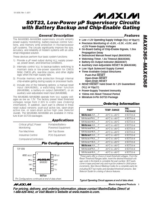
MAX6365–MAX6368
SOT23, Low-Power µP Supervisory Circuits with Battery Backup and Chip-Enable Gating
ABSOLUTE MAXIMUM RATINGS
Terminal Voltages (with respect to GND)
SOT23 Pin Configurations continued at end of data sheet.
Typical Operating Circuit appears at end of data sheet.
________________________________________________________________ Maxim Integrated Products 1
Pin Configurations
TOP VIEW
RESET, RESET 1 CE IN 2 GND 3 MR 4
MAX6365
8 CE OUT 7 BATT 6 OUT 5 VCC
Features
o Low +1.2V Operating Supply Voltage (VCC or VBATT) o Precision Monitoring of +5.0V, +3.3V, +3.0V, and
VCC, BATT, OUT.......................................................-0.3V to +6V RESET (open drain), RESET (open drain) ................-0.3V to +6V BATT ON, RESET (push-pull), RESET IN,
高安美厚模快的工作原理使用手册

高安美GAM QRC CMQ超级开关电源模块使用手册高安美GAM 行同步CMT超级开关电源模块使用手册序言/3214136@ 开关电源在电视机类电器上的应用已普及,其占整机的故障率和维修费较高,又往往是负载短路故障连损开关电源,容易损坏一大片元件,有不少疑难故障,软故障易不定时反复。
稳压控制原理五花八门难学难分析难掌握,有的根本找不到原理介绍资料,有的本身设计存在缺陷,绝大多数是技术过时的落后产品,过流保护形同虚设,输出短路故障烧,进线电源整流+300电源主滤波电容失效、脱焊烧,电网电压低也烧。
即使是最简单目前仍然生产的三洋80、A3电源也是原理分析争论文章不断,疑难故障连连。
有的找不到图纸,维修技术难度很高,储备所需IC特别是厚膜、小三极管、双极开关管、场效应开关管型号很多和占用资金多,备用的电源元件有不少用不上而贬值和浪费,很多元件不知也无法测量其参数,难购买,假货又多,上锡商家不包换。
有时软故障造成电源过热或屡损电源即使维修高手在有图纸有示波器的情况下也一筹莫展,需要的资料和时间很多,劳民伤财,损失很大,苦不堪言。
更倒霉的,因原机的元件低劣或老化或虚焊或电路板断裂,维修时或维修后短期内出现行+B高压打坏显像管的事例不少,弄不好就赔惨了。
相对而言,如STRM、STRF、STRG、STRW、KA2S、KA3S、KA5Q类场效应开关管厚膜IC要简单好修一些,但由外围元件故障引起的疑难故障和屡损电源IC现象仍会发生,且价格高昂,型号也过多,购买费用高花时间长而误工,有些根本买不到,假货多难辨真伪,拆机件很多是坏件,电源厚膜IC商家不包换,维修时仍忐忑不安。
有一些日本、韩国的厚膜IC价格奇高,严重受制。
老机型IC 停产没有卖。
二手100V AC电视机电源100%使用220V/110V工频变压器成本高且易损,厚膜IC只能买拆机件。
有不少人在电源难于修理的情况下只好用技术过时、功率达不到标称值、有干扰、质量又很差且匹配并不好的80P、83P、A3、UC3842(PRC)高价电源整板代用(也会屡损功率管),改装难度高,费时费力。
科尔摩根AKM 同步伺服电机 选型指南说明书
K O L L M O R G E N | A K o l l m o r g e n C O M PA N Y欢迎来到科尔摩根官方微信科尔摩根3目录u AKM ™ 同步伺服电机4u AKD ™ 伺服驱动器8u AKM ™ 各种选件12u AKM ™ 防水型和食品级防水型电机13u AKM ™ 系统综述14u AKM ™ 图纸和性能数据AKM1x 16AKM2x 20AKM3x24AKM4x 28AKM5x 34AKM6x 40AKM7x 44AKM8x48u L 10 轴承疲劳寿命和轴负载53u 反馈选件56u 抱闸选件60u 伺服电机连接器选件61u 型号命名67u MOTIONEERING ® Online71科尔摩根A K M 同步伺服电机选型指南克服设计、采购和时间障碍科尔摩根明白:帮助原始设备制造商的工程师克服障碍,可以显著提高其工作成效。
因而,我们主要通过如下三种方式来提供帮助:集成标准和定制产品在很多情况下,理想方案都不是一成不变的。
我们拥有专业应用知识,可以根据全面的产品组合来修改标准产品或开发全定制解决方案,从而为设计奠定良好的基础。
提供运动控制解决方案而不仅仅是部件在各公司减少供应商数量和工程人力的过程中,他们需要一家能够提供多种集成解决方案的全系统供应商。
科尔摩根就采用了全面响应模式,为客户提供全套解决方案,这些方案将编程软件、工程服务以及同类优秀的运动控制部件结合起来。
覆盖全球我们在美洲、欧洲、中东和亚洲拥有众多直销、工程支持单位、生产工厂以及分销商,临近全球各地的原始设备制造商。
这种便利优势可以加速我们的供货过程,根据客户需要随时随地供货。
财务和运营稳定性科尔摩根隶属于Fortive 公司。
Fortive 业务系统是推动Fortive 各部门发展的一个关键力量。
该系统采用“不断改善”(Kaizen )原理。
由高素质人才构成的多学科团队使用世界级的工具对过程进行评估,并制定相关计划以达到卓越的性能。
PR 品牌 6331 二线制可编程变送器 温度 安全 通信接口 多功能 隔离器 数字显示表 No.
产品手册6331二线制可编程变送器 安全栅 | 通讯接口 | 多功能 | 隔离器 | 数显表No. 6331V108-CN自此序列号始:2217922506 大特色产品满足您的一切需求凭借创新型专利技术,信号调节更加简单、智能。
产品组合由六大产品类组成,具备多种模拟量和数字量模块,涵盖上千种工业自动化应用。
所有产品都符合甚至高于行业的最高标准。
这可确保产品即便在最恶劣的环境条件下仍能可靠运行。
5 年产品保修期,让您使用更安心。
单品出色,组合无敌温度变送器和温度传感器系列产品,提供从温度测量点到系统控制一站式信号解决方案,从而在最大程度上保证信号的完整性。
仅需一套点对点解决方案,您就可以在任何环境中将工业过程中的温度信号转换为模拟量信号、总线信号或数字通讯信号。
该方案具备响应时间短,自动校准,传感器故障检测,低漂移和卓越 EMC 性能等诸多优点。
单品为多功能系列产品,可涵盖大量现场应用,可轻而易举按照您的现场标准进行配置。
此种单品可适用多种应用方式,既节省安装和培训时间,又大大简化库存备件管理。
该设备专为长期信号精度高、功耗低、抗电噪声优异、编程简单而设计。
我们提供经济实惠、使用方便、面向未来的通讯接口,以便您能够访问所安装的 PR 产品。
所有接口均可拆卸,并带有屏幕和按钮,可以显示过程值/诊断值和对参数进行配置。
产品特定功能包括通过 Modbus 和蓝牙进行通讯,以及使用我们的 PR 过程主管 (PPS) 应用程序进行远程访问,适用于 iOS和Android 等终端。
数显表系列以其灵活性和稳定性著称。
该设备系列几乎满足过程信号读数显示的所有需求,并具有通用的输入和供电能力。
无论哪种行业,无论环境条件何其苛刻,该设备均能实时测量过程值并提供用户友好型界面和值得信赖的继电器信号。
我们采用最严格的安全标准来检验产品,以期提供最安全的信号。
秉承创新精神,我们已经在 SIL 2 全面评估本质安全型接口方面取得了开创性成就,其既高效又经济,效果卓著,成效斐然。
MEMORY存储芯片MAX823TEUK+T中文规格书
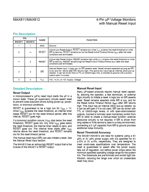
Manual Reset Input Many μP-based products require manual reset capabil -ity, allowing the operator, a test technician, or external logic circuitry to initiate a reset. A logic low on MR asserts reset. Reset remains asserted while MR is low, and for the Reset Active Timeout Period (t RP ) after MR returns high. This input has an internal 20kΩ pull-up resistor, so it can be left open if it is not used. MR can be driven with TTL or CMOS-logic levels, or with open-drain/collector outputs. Connect a normally open momentary switch from MR to GND to create a manual-reset function; external debounce circuitry is not required. If MR is driven from long cables or if the device is used in a noisy environment, connecting a 0.1μF capacitor from MR to ground provides additional noise immunity.Reset Threshold Accuracy The MAX811/MAX812 are ideal for systems using a 5V ±5% or 3V ±5% power supply with ICs specified for 5V ±10% or 3V ±10%, respectively. They are designed to meet worst-case specifications over temperature. The reset is guaranteed to assert after the power supplyfalls out of regulation, but before power drops below theminimum specified operating voltage range for the systemICs. The thresholds are pre-trimmed and exhibit tight dis -tribution, reducing the range over which an undesirable reset may occur.PINNAME FUNCTION MAX811MAX81211GND Ground 2—RESET Active-Low Reset Output. RESET remains low while V CC is below the reset threshold or while MR is held low. RESET remains low for the Reset Active Timeout Period (t RP ) after the reset conditions are terminated.—2RESET Active-High Reset Output. RESET remains high while V CC is below the reset threshold or while MR is held low. RESET remains high for Reset Active Timeout Period (t RP ) after the reset conditions are terminated.33MR Manual Reset Input. A logic low on MR asserts reset. Reset remains asserted as long as MR is low and for 180ms after MR returns high. This active-low input has an internal 20kΩ pull-up resistor. It can be driven from a TTL or CMOS-logic line, or shorted to ground with a switch. Leave open if unused.44V CC +5V, +3.3V, or +3V Supply Voltage Detailed DescriptionReset OutputA microprocessor’s (μP’s) reset input starts the μP in aknown state. These μP supervisory circuits assert resetto prevent code execution errors during power-up, power-down, or brownout conditions.RESET is guaranteed to be a logic low for V CC > 1V.Once V CC exceeds the reset threshold, an internal timerkeeps RESET low for the reset timeout period; after thisinterval, RESET goes high.If a brownout condition occurs (V CC dips below the resetthreshold), RESET goes low. Any time V CC goes belowthe reset threshold, the internal timer resets to zero, andRESET goes low. The internal timer starts after V CC returns above the reset threshold, and RESET remainslow for the reset timeout period.The manual reset input (MR ) can also initiate a reset. See the Manual Reset Input section.The MAX812 has an active-high RESET output that is theinverse of the MAX811’s RESET output.MAX811/MAX8124-Pin μP Voltage Monitorswith Manual Reset InputPin DescriptionTerminal Voltage (with respect to GND)V CC.....................................................................-0.3V to 6.0V All Other Inputs .....................................-0.3V to (V CC + 0.3V) Input Current, V CC, MR......................................................20mA Output Current, RESET or RESET ....................................20mA Continuous Power Dissipation (T A = +70°C)SOT143 (derate 4mW/°C above +70°C) .....................320mW Operating Temperature Range ...........................-40°C to +85°C Junction Temperature ......................................................+150°C Storage Temperature Range ............................-65°C to +160°C Lead Temperature (soldering, 10sec) .............................+300°C(V CC = 5V for L/M versions, V CC = 3.3V for T/S versions, V CC = 3V for R version, T A = -40°C to +85°C, unless otherwise noted. Typical values are at T A = +25°C.) (Note 1)PARAMETER SYMBOL CONDITIONS MIN TYP MAX UNITSOperating Voltage Range V CC T A = 0°C to +70°C 1.0 5.5V T A = -40°C to +85°C 1.2Supply Current I CC MAX81_L/M, V CC = 5.5V, I OUT = 0615µA MAX81_R/S/T, V CC = 3.6V, I OUT = 0 2.710Reset Threshold V TH MAX81_LT A = +25°C 4.54 4.63 4.72V T A = -40°C to +85°C 4.50 4.75MAX81_MT A = +25°C 4.30 4.38 4.46T A = -40°C to +85°C 4.25 4.50MAX81_TT A = +25°C 3.03 3.08 3.14T A = -40°C to +85°C 3.00 3.15MAX81_ST A = +25°C 2.88 2.93 2.98T A = -40°C to +85°C 2.85 3.00MAX81_RT A = +25°C 2.58 2.63 2.68T A = -40°C to +85°C 2.55 2.70Reset Threshold Tempco30ppm/°CV CC to Reset Delay (Note 2)V OD = 125mV, MAX81_L/M40µs V OD = 125mV, MAX81_R/S/T20Reset Active Timeout Period t RP V CC = V TH(MAX)140560ms MR Minimum Pulse Width t MR10µs MR Glitch Immunity (Note 3)100ns MR to Reset PropagationDelay (Note 2)t MD0.5µsMR Input Threshold V IHV CC > V TH(MAX), MAX81_L/M2.3V V IL0.8V IHV CC > V TH(MAX), MAX81_R/S/T0.7 x V CCV IL0.25 x V CCMR Pull-Up Resistance102030kΩRESET Output Voltage (MAX812)V OH I SOURCE = 150µA, 1.8V < V CC < V TH(MIN)0.8 x V CCV V OLMAX812R/S/T only, I SINK = 1.2mA,V CC = V TH(MAX)0.3MAX812L/M only, I SINK = 3.2mA,V CC = V TH(MAX)0.4MAX811/MAX8124-Pin μP Voltage Monitorswith Manual Reset Input Absolute Maximum RatingsStresses beyond those listed under “Absolute Maximum Ratings” may cause permanent damage to the device. These are stress ratings only, and functional operation of the device at these or any other conditions beyond those indicated in the operational sections of the specifications is not implied. Exposure to absolute maximum rating conditions for extended periods may affect device reliability.Electrical Characteristics。
迈普路由器产品手册

迈普路由器产品手册This model paper was revised by the Standardization Office on December 10, 2020目录一、迈普路由器产品系列1MP8800系列万兆核心路由器1.1产品概述MP8800系列路由器是迈普通信技术股份有限公司自主研发的,全球第一款采用众核技术的路由器,是基于对行业用户业务应用的充分调研和深刻理解而推出的一款跨时代的万兆级高端骨干核心路由器。
MP8800基于先进的众核设计理念,采用分布式处理架构,充分考虑云网络针对业务、内容的数据处理特点,可实现客户业务的开放化和业务的云端化。
通过迈普特有的多线程专利处理技术和先进的众核处理器硬件,实现高速的IPv4/IPv6、MPLS转发,整机的包转发性能高达800Mpps,强大的转发性能和丰富的业务特性全面满足用户各种组网应用的需求。
MP8800系列路由器作为一种多用途的高端骨干核心路由器主要应用于IP骨干网、IP城域网以及各种大型IP网络的核心和汇聚位置。
MP8800路由器的强大转发性能和丰富的业务能力能够全面满足用户多种组网应用需求,可与迈普全系列路由器一起为运营商、金融、政府、能源、交通、教育、军队等行业用户和大中型企业用户提供整网解决方案。
1.2产品特征全球领先的众核技术,丰富的业务支持能力MP8800系列万兆核心路由器采用业界领先的众核处理器,是全球第一款众核高端路由器。
它基于先进的众核设计理念,充分考虑云网络针对业务、内容的数据处理特点,实现客户业务的开放化和业务的云端化。
支持用户程序独立占有CPU核组,可独立计算,独立完成自定义的业务功能,并实现云端业务,防病毒,邮件过滤,安全准入控制等应用。
线速转发能力,支持可扩展的交换容量采用先进的分布式处理架构,集中式控制,分布式处理,充分保证每个槽位的线速处理能力,系统具有优越的可扩展性。
通过迈普特有的多线程专利处理技术和众核处理器,保障多个处理内核之间数据转发和负载均衡,实现高速的IPv4/IPv6、MPLS转发。
BUF634中文资料

1 Feature 1特点•High Output Current: 250 mA•高输出电流:250毫安•Slew Rate: 2000 V/µs •摆率(电压转换速率):2000 V /µS•Pin-Selected Bandwidth: 30 MHz to 180 MHz •引脚选择带宽:30兆赫至180兆赫•Low Quiescent Current: 1.5 mA (30 MHz BW) •低静态输出电流:1.5毫安(30兆赫带宽)•Wide Supply Range: ±2.25 to ±18 V •宽电压供应范围:2.25至18伏•Internal Current Limit •内部电流限制•Thermal Shutdown Protection •热关机保护•8-Pin PDIP, SOIC-8, 5-Lead TO-220, 5-Lead DDPAK-TO-263 Surface-Mount•8引脚PDIP,SOIC - 8、5引脚TO - 220,5引脚ddpak-to-263表面贴装2 Applications 2应用•Valve Driver •阀门驱动器•Solenoid Driver•螺线管(电磁)驱动器•Op Amp Current Booster•运算放大器电流放大器•Line Driver•线路驱动器•Headphone Driver•耳机驱动器•Video Driver•视频驱动程序•Motor Driver •电机驱动•Test Equipment•测试设备•ATE Pin Driver•ATE自测引脚驱动程序3 Description3 描述The BUF634 device is a high speed, unity-gain open-loop buffer recommended for a wide range of applications. The BUF634 device can be used inside the feedback loop of op amps to increase output current, eliminate thermal feedback, and improve capacitive load drive.是一种高速开环增益缓冲器广泛的应用范围中的建议,它可用于运算放大器的反馈环路内,一起增加输出电流消除热反馈和改善容性负载驱动。
莫加PT-G7728系列28口层2全Gigabit可扩展管理以太网交换机产品说明书

PT-G7728SeriesIEC61850-328-port Layer2full Gigabit modular managed Ethernet switchesFeatures and Benefits•IEC61850-3Edition2Class2compliant•Hot-swappable interface and power modules for continuous operation•Built-in MMS server based on IEC61850-90-4switch data modeling forpower SCADA•IEEE1588hardware time stamp supportedCertificationsIntroductionThe PT-G7728modular switches provide up to28Gigabit ports,including4fixed ports,6interface module slots,and2power module slots to ensure sufficient flexibility for a variety of applications.The PT-G7728Series is designed to meet evolving network requirements,including a hot-swappable module design that enables you to change or add devices without shutting down your device.The multiple Ethernet modules(RJ45,SFP,and PoE)and power units(24/48VDC,110/220VAC/VDC)provide even greater flexibility as well as suitability for different operating conditions.The switches support a full Gigabit platform that provides enough bandwidth to set up an Ethernet backbone.Certifications include IEC61850Edition2Class2to ensure high availability and wide usage.SpecificationsEthernet Interface10/100/1000BaseT(X)Ports(RJ45connector)2100/1000BaseSFP Ports2Module6Slot Combination See the LM-7000H datasheet for Ethernet and PoE+modules informationStandards IEEE802.3for10BaseTIEEE802.3u for100BaseT(X)and100BaseFXIEEE802.3ab for1000BaseT(X)IEEE802.3z for1000BaseXIEEE802.1D-2004for Spanning Tree ProtocolIEEE802.1w for Rapid Spanning Tree ProtocolIEEE802.1p for Class of ServiceIEEE802.1Q for VLAN TaggingIEEE802.1X for authenticationIEEE802.3ad for Port Trunk with LACPIEEE802.3x for flow controlEthernet Software FeaturesManagement IPv4/IPv6,SNMP Inform,SNMPv1/v2c/v3,DHCP Server/Client,DHCP Option66/67/82,BOOTP,TFTP,LLDP,RARP,HTTP,HTTPS,Telnet,Flow control,Back Pressure FlowControl,Port Mirror,Fiber check,Dying Gasp,SMTP,SyslogMIB MIB-II,Ethernet-like MIB,Bridge MIB,P-BRIDGE MIB,Q-BRIDGE MIB,RSTP MIB,RMON MIB Groups1,2,3,9Filter IGMP v1/v2/v3,GMRP,GVRP,802.1Q,QinQ VLANRedundancy Protocols Link Aggregation,MSTP,RSTP,STP,Turbo Chain,Turbo Ring v1/v2,V-ONSecurity RADIUS,TACACS+,SSH,Port Lock,Broadcast storm protection,MAB authentication,Sticky MAC,Access control listTime Management NTP Server/Client,SNTP,IEEE1588v2PTP(hardware-based)Power Substation IEC61850QoS,GOOSE CheckIndustrial Protocols EtherNet/IP,Modbus TCPSwitch PropertiesPriority Queues8Max.No.of VLANs512VLAN ID Range1to4094IGMP Groups4096MAC Table Size16KPacket Buffer Size12MbitsJumbo Frame Size9.6KBSerial InterfaceConsole Port Micro USB Type BUSB InterfaceStorage Port USB Type APower ParametersInput Voltage with PWR-HV-P48installed:110/220VDC/VAC for the switch system48VDC for PoE system(53to57VDC is recommended for PoE+devices)with PWR-LV-P48installed:24/48VDC for the switch system48VDC for PoE system(53to57VDC is recommended for PoE+devices)with PWR-HV-NP installed:110/220VDC/VAC for the switch systemwith PWR-LV-NP installed:24/48VDC for the switch systemOperating Voltage with PWR-HV-P48installed:88to300VDC,90to264VAC for the switch system46to57VDC for PoE systemswith PWR-LV-P48installed:18to72VDC for the switch system46to57VDC for PoE systemswith PWR-HV-NP installed:88to300VDC,90to264VAC for the switch systemwith PWR-LV-NP installed:18to72VDC for the switch systemInput Current with PWR-HV-P48installed:PWR input current(switch system)Max.0.11A@110VDCMax.0.06A@220VDCMax.0.29A@110VACMax.0.18A@220VACEPS input current(PoE system)Max.0.53A@48VDC(excluding power consumption of PoE devices)with PWR-LV-P48installed:PWR input current(switch system)Max.0.53A@24VDCMax.0.28A@48VDCEPS input current(PoE system)Max.0.53A@48VDC(excluding power consumption of PoE devices)with PWR-HV-NP installed:PWR input current(switch system)Max.0.11A@110VDCMax.0.06A@220VDCMax.0.29A@110VACMax.0.18A@220VACwith PWR-LV-NP installed:PWR input current(switch system)Max.0.53A@24VDCMax.0.28A@48VDCPhysical CharacteristicsIP Rating IP30Dimensions443x44x280mm(17.44x1.73x11.02in)Weight3080g(6.8lb)Installation19-inch rack mountingEnvironmental LimitsOperating Temperature-40to85°C(-40to185°F)Storage Temperature(package included)-40to85°C(-40to185°F)Ambient Relative Humidity5to95%(non-condensing)Standards and CertificationsEMC EN55032/24EMI CISPR32,FCC Part15B Class AEMS IEC61000-4-2ESD:Contact:8kV;Air:15kVIEC61000-4-3RS:80MHz to1GHz:20V/mIEC61000-4-4EFT:Power:4kV;Signal:4kVIEC61000-4-5Surge:Power:4kV;Signal:4kVIEC61000-4-6CS:10VIEC61000-4-8PFMFPower Substation IEC61850-3Edition2.0Class2,IEEE1613Railway EN50121-4Safety EN62368-1,UL62368-1MTBFTime449,542hrsStandards Telcordia(Bellcore),GBWarrantyWarranty Period5yearsDetails See /warrantyPackage ContentsDevice1x PT-G7728Series switchCable USB cable(Type A male to Micro USB type B)Installation Kit2x cap,for Micro-B USB port1x cap,metal,for ABC-02USB storage port2x rack-mounting ear2x cap,plastic,for SFP slotDocumentation1x quick installation guide1x warranty card1x substance disclosure table1x product certificates of quality inspection,Simplified Chinese1x product notice,Simplified ChineseNote SFP modules,modules from the LM-7000H Module Series,and/or modules from thePWR Power Module Series need to be purchased separately for use with this product.DimensionsOrdering InformationModel Name Layer 100/1000Base SFPSlots10/100/1000BaseT(X)PortsRJ45ConnectorPoE Ports,10/100/1000Base T(X)RJ45ConnectorOperating Temp.PT-G772822to262to260to24-40to85°C Accessories(sold separately)Storage KitsABC-02-USB Configuration backup and restoration tool,firmware upgrade,and log file storage tool for managedEthernet switches and routers,0to60°C operating temperatureABC-02-USB-T Configuration backup and restoration tool,firmware upgrade,and log file storage tool for managedEthernet switches and routers,-40to75°C operating temperaturePower SuppliesPWR-HV-P48Power supply module(110/220VAC/VDC)with system power input,relay,PoE power inputPWR-LV-P48Power supply module(24/48VDC)with system power input,relay,PoE power inputPWR-HV-NP Power supply module(110/220VAC/VDC)with system power input,relayPWR-LV-NP Power supply module(24/48VDC)with system power input,relayLM-7000H Module SeriesLM-7000H-4GTX Gigabit Ethernet module with410/100/1000BaseT(X)portsLM-7000H-4GSFP Gigabit Ethernet module with4100/1000BaseSFP slotsLM-7000H-4GPoE Gigabit Ethernet module with410/100/1000BaseT(X)IEEE802.3af/at PoE+portsLM-7000H-4TX Fast Ethernet module with410/100BaseT(X)portsLM-7000H-4PoE Fast Ethernet module with410/100BaseT(X)IEEE802.3af/at PoE+portsSFP ModulesSFP-1FELLC-T SFP module with1100Base single-mode with LC connector for80km transmission,-40to85°Coperating temperatureSFP-1FEMLC-T SFP module with1100Base multi-mode,LC connector for2/4km transmission,-40to85°C operatingtemperatureSFP-1FESLC-T SFP module with1100Base single-mode with LC connector for40km transmission,-40to85°Coperating temperatureSFP-1GEZXLC SFP module with11000BaseEZX port with LC connector for110km transmission,0to60°C operatingtemperatureSFP-1G10ALC WDM-type(BiDi)SFP module with11000BaseSFP port with LC connector for10km transmission;TX1310nm,RX1550nm,0to60°C operating temperatureSFP-1G10ALC-T WDM-type(BiDi)SFP module with11000BaseSFP port with LC connector for10km transmission;TX1310nm,RX1550nm,-40to85°C operating temperatureSFP-1G10BLC WDM-type(BiDi)SFP module with11000BaseSFP port with LC connector for10km transmission;TX1550nm,RX1310nm,0to60°C operating temperatureSFP-1G10BLC-T WDM-type(BiDi)SFP module with11000BaseSFP port with LC connector for10km transmission;TX1550nm,RX1310nm,-40to85°C operating temperatureSFP-1G20ALC WDM-type(BiDi)SFP module with11000BaseSFP port with LC connector for20km transmission;TX1310nm,RX1550nm,0to60°C operating temperatureSFP-1G20ALC-T WDM-type(BiDi)SFP module with11000BaseSFP port with LC connector for20km transmission;TX1310nm,RX1550nm,-40to85°C operating temperatureSFP-1G20BLC WDM-type(BiDi)SFP module with11000BaseSFP port with LC connector for20km transmission;TX1550nm,RX1310nm,0to60°C operating temperatureSFP-1G20BLC-T WDM-type(BiDi)SFP module with11000BaseSFP port with LC connector for20km transmission;TX1550nm,RX1310nm,-40to85°C operating temperatureSFP-1G40ALC WDM-type(BiDi)SFP module with11000BaseSFP port with LC connector for40km transmission;TX1310nm,RX1550nm,0to60°C operating temperatureSFP-1G40ALC-T WDM-type(BiDi)SFP module with11000BaseSFP port with LC connector for40km transmission;TX1310nm,RX1550nm,-40to85°C operating temperatureSFP-1G40BLC WDM-type(BiDi)SFP module with11000BaseSFP port with LC connector for40km transmission;TX1550nm,RX1310nm,0to60°C operating temperatureSFP-1G40BLC-T WDM-type(BiDi)SFP module with11000BaseSFP port with LC connector for40km transmission;TX1550nm,RX1310nm,-40to85°C operating temperatureSFP-1GEZXLC-120SFP module with11000BaseEZX port with LC connector for120km transmission,0to60°C operatingtemperatureSFP-1GLHLC SFP module with11000BaseLH port with LC connector for30km transmission,0to60°C operatingtemperatureSFP-1GLHLC-T SFP module with11000BaseLH port with LC connector for30km transmission,-40to85°C operatingtemperatureSFP-1GLHXLC SFP module with11000BaseLHX port with LC connector for40km transmission,0to60°C operatingtemperatureSFP-1GLHXLC-T SFP module with11000BaseLHX port with LC connector for40km transmission,-40to85°Coperating temperatureSFP-1GLSXLC SFP module with11000BaseLSX port with LC connector for1km/2km transmission,0to60°Coperating temperatureSFP-1GLSXLC-T SFP module with11000BaseLSX port with LC connector for1km/2km transmission,-40to85°Coperating temperatureSFP-1GLXLC SFP module with11000BaseLX port with LC connector for10km transmission,0to60°C operatingtemperatureSFP-1GLXLC-T SFP module with11000BaseLX port with LC connector for10km transmission,-40to85°C operatingtemperatureSFP-1GSXLC SFP module with11000BaseSX port with LC connector for300m/550m transmission,0to60°Coperating temperatureSFP-1GSXLC-T SFP module with11000BaseSX port with LC connector for300m/550m transmission,-40to85°Coperating temperatureSFP-1GZXLC SFP module with11000BaseZX port with LC connector for80km transmission,0to60°C operatingtemperatureSFP-1GZXLC-T SFP module with11000BaseZX port with LC connector for80km transmission,-40to85°C operatingtemperatureSoftwareMXview-50Industrial network management software with a license for50nodes(by IP address)MXview-100Industrial network management software with a license for100nodes(by IP address)MXview-250Industrial network management software with a license for250nodes(by IP address)MXview-500Industrial network management software with a license for500nodes(by IP address)MXview-1000Industrial network management software with a license for1000nodes(by IP address)MXview-2000Industrial network management software with a license for2000nodes(by IP address)MXview Upgrade-50License expansion of MXview industrial network management software by50nodes(by IP address)©Moxa Inc.All rights reserved.Updated May28,2020.This document and any portion thereof may not be reproduced or used in any manner whatsoever without the express written permission of Moxa Inc.Product specifications subject to change without notice.Visit our website for the most up-to-date product information.。
MX636JH中文资料

General DescriptionThe MX536A and MX636 are true RMS-to-DC convert-ers. They feature low power and are designed to accept low-level input signals from 0 to 7V RMS for the MX536A and 0 to 200mV RMS for the MX636. Both devices accept complex input waveforms containing AC and DC com-ponents. They can be operated from either a single sup-ply or dual supplies. Both devices draw less than 1mA of quiescent supply current, making them ideal for bat-tery-powered applications.Input and output offset, positive and negative waveform symmetry (DC reversal), and full-scale accuracy are laser trimmed, so that no external trims are required to achieve full rated accuracy.________________________ApplicationsDigital MultimetersBattery-Powered Instruments Panel Meters Process Control____________________________Featureso True RMS-to-DC Conversiono Computes RMS of AC and DC Signals o Wide Response:2MHz Bandwidth for V RMS > 1V (MX536A)1MHz Bandwidth for V RMS > 100mV (MX636)o Auxiliary dB Output:60dB Range (MX536A)50dB Range (MX636)o Single- or Dual-Supply Operation o Low Power: 1.2mA typ (MX536A)800µA typ (MX636)MX536A/MX636True RMS-to-DC Converters________________________________________________________________Maxim Integrated Products1Pin Configurations_________Typical Operating Circuits19-0824; Rev 2; 3/96Ordering Information continued at end of data sheet.*Maxim reserves the right to ship ceramic packages in lieu of CERDIP packages.** Dice are specified at T A = +25°C.For free samples & the latest literature: , or phone 1-800-998-8800.For small orders, phone 408-737-7600 ext. 3468.M X 536A /M X 636True RMS-to-DC Converters 2_______________________________________________________________________________________ABSOLUTE MAXIMUM RATINGSELECTRICAL CHARACTERISTICS—MX536A(T A = +25°C, +V S = +15V, -V S = -15V, unless otherwise noted.)Stresses beyond those listed under “Absolute Maximum Ratings” may cause permanent damage to the device. These are stress ratings only, and functional operation of the device at these or any other conditions beyond those indicated in the operational sections of the specifications is not implied. Exposure to absolute maximum rating conditions for extended periods may affect device reliability.Supply Voltage:Dual Supplies (MX536A)............................±18V(MX636).............................±12VSingle Supply (MX536A)...........................+36V(MX636).............................+24VInput Voltage (MX536A).......................................................±25V(MX636).........................................................±12VPower Dissipation (Package)Plastic DIP (derate 12mW/°C above +75°C)...............450mW Small Outline (derate 10mW/°C above +75°C)............400mW Ceramic (derate 10mW/°C above +75°C)...................500mW TO-100 metal can (derate 7mW/°C above +75°C)......450mWOutput Short-Circuit Duration........................................Indefinite Operating Temperature RangesCommercial (J, K)...............................................0°C to +70°C Military (S)......................................................-55°C to +125°C Storage Temperature Range.............................-55°C to +150°C Lead Temperature (soldering, 10sec)................................300°CMX536A/MX636True RMS-to-DC Converters_______________________________________________________________________________________3ELECTRICAL CHARACTERISTICS—MX536A (continued)(T A = +25°C, +V S = +15V, -V S = -15V, unless otherwise noted.)M X 536A /M X 636True RMS-to-DC Converters 4_______________________________________________________________________________________ELECTRICAL CHARACTERISTICS—MX536A (continued)(T A = +25°C, +V S = +15V, -V S = -15V, unless otherwise noted.)ELECTRICAL CHARACTERISTICS—MX636(T A = +25°C, +V S = +3V, -V S = -5V, unless otherwise noted.)MX536A/MX636True RMS-to-DC Converters_______________________________________________________________________________________5ELECTRICAL CHARACTERISTICS—MX636 (continued)(T= +25°C, +V = +3V, -V = -5V, unless otherwise noted.)M X 536A /M X 636_______________Detailed DescriptionThe MX536A/MX636 uses an implicit method of RMS computation that overcomes the dynamic range as well as other limitations inherent in a straightforward compu-tation of the RMS. The actual computation performed by the MX536A/MX636 follows the equation:V RMS = Avg. [V IN 2/V RMS ]The input voltage, V IN , applied to the MX536A/MX636 is processed by an absolute-value/voltage to current con-verter that produces a unipolar current I 1(Figure 1).This current drives one input of a squarer/divider that produces a current I 4that has a transfer function:I 4= I 12I 3The current I 4drives the internal current mirror through a lowpass filter formed by R1 and an external capaci-tor, C AV . As long as the time constant of this filter is greater than the longest period of the input signal, I 4is averaged. The current mirror returns a current, I 3, to the square/divider to complete the circuit. The current I 4is then a function of the average of (I 12/I 4), which is equal to I 1RMS .The current mirror also produces a 2 · I 4output current,I OUT , that can be used directly or converted to a volt-age using resistor R2 and the internal buffer to provide a low-impedance voltage output. The transfer function for the MX536A/MX636 is:V OUT = 2 · R2 · I RMS = V INThe dB output is obtained by the voltage at the emitter of Q3, which is proportional to the -log V IN . The emitter follower Q5 buffers and level shifts this voltage so that the dB output is zero when the externally set emitter current for Q5 approximates I 3.Standard Connection(Figure 2)The standard RMS connection requires only one exter-nal component, C AV . In this configuration the MX536A/MX636 measures the RMS of the AC and DC levels present at the input, but shows an error for low-frequency inputs as a function of the C AV filter capaci-tor. Figure 3 gives practical values of C AV for various values of averaging error over frequency for the stan-dard RMS connections (no post filtering). If a 3µF capacitor is chosen, the additional error at 100Hz will be 1%. If the DC error can be rejected, a capacitor should be connected in series with the input, as would typically be the case in single-supply operation.The input and output signal ranges are a function of the supply voltages. Refer to the electrical characteristics for guaranteed performance. The buffer amplifier can be used either for lowering the output impedance of the cir-cuit, or for other applications such as buffering high-impedance input signals. The MX536A/MX636 can be used in current output mode by disconnecting the inter-nal load resistor, R L , from ground. The current output is available at pin 8 (pin 10 on the “H” package) with a nominal scale of 40µA/V RMS input for the MX536A and 100µA/V RMS input for the MX636. The output is positive.True RMS-to-DC Converters 6_______________________________________________________________________________________ELECTRICAL CHARACTERISTICS—MX636 (continued)(T= +25°C, +V = +3V, -V = -5V, unless otherwise noted.)Note 1:Accuracy is specified for 0 to 7V RMS , DC or 1kHz sine-wave input with the MX536A connected as in Figure 2.Note 2:Error vs. crest factor is specified as an additional error for 1V RMS rectangular pulse stream, pulse width = 200µs.Note 3:Input voltages are expressed in volts RMS, and error as % of reading.Note 4:With 2k Ωexternal pull-down resistor.Note 5:Accuracy is specified for 0 to 200mV, DC or 1kHz sine-wave input. Accuracy is degraded at higher RMS signal levels.Note 6:Measured at pin 8 of DIP and SO (I OUT ), with pin 9 tied to COMMON.Note 7:Error vs. crest factor is specified as an additional error for 200mV RMS rectangular pulse input, pulse width = 200µs.Note 8:Input voltages are expressed in volts RMS.Note 9:With 10k Ωexternal pull-down resistor from pin 6 (BUF OUT) to -V S .Note 10:With BUF input tied to COMMON.MX536A/MX636True RMS-to-DC Converters_______________________________________________________________________________________7Figure 1. MX536A Simplified SchematicFigure 2. MX536A/MX636 Standard RMS ConnectionM X 536A /M X 636High-Accuracy AdjustmentsThe accuracy of the MX536A/MX636 can be improved by the addition of external trims as shown in Figure 4.R4 trims the offset. The input should be grounded and R4 adjusted to give zero volts output from pin 6. R1 is trimmed to give the correct value for either a calibrated DC input or a calibrated AC signal. For example: 200mV DC input should give 200mV DC output; a ±200mV peak-to-peak sine-wave should give 141mV DC output.Single-Supply OperationBoth the MX536A and the MX636 can be used with a single supply down to +5V (Figure 5). The major limita-tion of this connection is that only AC signals can be measured, since the differential input stage must be biased off ground for proper operation. The load resis-tor is necessary to provide output sink current. The input signal is coupled through C2 and the value cho-sen so that the desired low-frequency break point is obtained with the input resistance of 16.7k Ωfor the MX536A and 6.7k Ωfor the MX636.Figure 5 shows how to bias pin 10 within the range of the supply voltage (pin 2 on “H” packages). It is critical that no extraneous signals are coupled into this pin. A capacitor connected between pin 10 and ground is recommended. The common pin requires less than 5µA of input current, and if the current flowing through resis-tors R1 and R2 is chosen to be approximately 10 times the common pin current, or 50µA, the resistor values can easily be calculated.Choosing the Averaging Time ConstantBoth the MX536A and MX636 compute the RMS value of AC and DC signals. At low frequencies and DC, the output tracks the input exactly; at higher frequencies,the average output approaches the RMS value of the input signal. The actual output differs from the ideal by an average (or DC) error plus some amount of ripple.The DC error term is a function of the value of C AV and the input signal frequency. The output ripple is inverse-True RMS-to-DC Converters 8_______________________________________________________________________________________Figure 3. Lower Frequency for Stated % of Reading Error and Settling Time for Circuit shown in Figure 2Figure 4. Optional External Gain and Output Offset TrimsFigure 5. Single-Supply Operationly proportional to the value of C AV . Waveforms with high crest factors, such as a pulse train with low duty cycle,should have an average time constant chosen to be at least ten times the signal period.Using a large value of C AV to remove the output ripple increases the settling time for a step change in the input signal level. Figure 3 shows the relationship between C AV and settling time, where 115ms settling equals 1µF of C AV . The settling time, or time for the RMS converter to settle to within a given percent of the change in RMS level, is set by the averaging time constant, which varies approximately 2:1 between increasing and decreasing input signals. For example, increasing input signals require 2.3 time constants to settle to within 1%, and 4.6time constants for decreasing signals levels.In addition, the settling time also varies with input signal levels, increasing as the input signal is reduced, and decreasing as the input is increased as shown in Figures 6a and 6b.Using Post FiltersA post filter allows a smaller value of C AV , and reduces ripple and improves the overall settling time. The value of C AV should be just large enough to give the maxi-mum DC error at the lowest frequency of interest. The post filter is used to remove excess output ripple.Figures 7, 8, and 9 give recommended filter connec-tions and values for both the MX536A and MX636.Table 1 lists the number of time constants required for the RMS section to settle to within different percentages of the final value for a step change in the input signal.Decibel Output (dB)The dB output of the MX536A/MX636 originates in the squarer/divider section and works well over a 60dB range. The connection for dB measurements is shown in Figure 10. The dB output has a temperature drift of 0.03dB/°C, and in some applications may need to be compensated. Figure 10 shows a compensation scheme. The amplifier can be used to scale the output for a particular application. The values used in Figure 10 give an output of +100mV/dB.MX536A/MX636True RMS-to-DC Converters_______________________________________________________________________________________910012.51m100m10157.5RMS INPUT LEVEL (V)S E T T L I N G T I M E R E L A T I V E T O 1V R M S I N P U T S E T T L I N G T I M E10mMX536AFigure 6a. MX536A Settling Time vs. Input Level 10012.51m100m157.5RMS INPUT LEVEL (V)S E T T L I N G T I M E R E L A T I V E T O 200m V R M S I N P U T S E T T L I N G T I M E10mMX636Figure 6b. MX636 Settling Time vs. Input LevelNote:(τ) Settling Times for Linear RC FilterM X 536A /M X 636Frequency ResponseThe MX536A/MX636 utilizes a logarithmic circuit in per-forming the RMS computation of the input signal. The bandwidth of the RMS converters is proportional to sig-nal level. Figures 11 and 12 represent the frequency response of the converters from 10mV to 7V RMS for the MX536A and 1mV to 1V for the MX636, respectively.The dashed lines indicate the upper frequency limits for 1%, 10%, and ±3dB of reading additional error.Caution must be used when designing RMS measuring systems so that overload does not occur. The input clipping level for the MX636 is ±12V, and for the MX536A it is ±20V. A 7V RMS signal with a crest factor of 3 has a peak input of 21V.Application in a Low-Cost DVMA low-cost digital voltmeter (DVM) using just two inte-grated circuits plus supporting circuitry and LCD dis-play is shown in Figure 13. The MAX130 is a 3 1/2 digit integrating A/D converter with precision bandgap refer-ence. The 10M Ωinput attenuator is AC coupled to pin 6 of the MX636 buffer amplifier. The output from the MX636 is connected to the MAX130 to give a direct reading to the LCD display.True RMS-to-DC Converters 10______________________________________________________________________________________Figure 7. MX536A/MX636 with a One-Pole Output FilterFigure 8. MX536A/MX636 with a Two-Pole Output FilterFigure 9. Performance Features of Various Filter Types for MX536A/MX636MX536A/MX636True RMS-to-DC Converters______________________________________________________________________________________11Figure 10. dB ConnectionFigure 12. MX636 High-Frequency ResponseFigure 11. MX536A High-Frequency Response*** Dice are specified at T A = +25°C.M X 536A /M X 636True RMS-to-DC Converters Pin Configurations (continued)Figure 13. Portable High-Z Input RMS DPM and dB MeterTypical Operating________________Circuits (continued)___________________________________________Ordering Information (continued)Maxim cannot assume responsibility for use of any circuitry other than circuitry entirely embodied in a Maxim product. No circuit patent licenses are implied. Maxim reserves the right to change the circuitry and specifications without notice at any time.12____________________Maxim Integrated Products, 120 San Gabriel Drive, Sunnyvale, CA 94086 408-737-7600©1998 Maxim Integrated ProductsPrinted USAis a registered trademark of Maxim Integrated Products.。
MAX31865中文资料_数据手册_参数

VIL
CS, SDI, SCLK
Input Logic 1
Analog Voltages (FORCE+,FORCE2, FORCE-, RTDIN+, RTDIN-) Reference Resistor Cable Resistance
VIH
CS, SDI, SCLK
Normal conversion results
MAX31865 RTD-to-Digital Converter
ABSOLUTE MAXIMUM RATINGS
Voltage Range on VDD Relative to GND1.............-0.3V to +4.0V Voltage Range on BIAS, REFIN+,
Applications
Industrial Equipment Medical Equipment Instrumentation
Ordering Information appears at end of data sheet.
For related parts and recommended products to use with this part, refer to /MAX31865.related.
PACKAGE THERMAL CHARACTERISTICS (Note 1)
TQFN Junction-to-Ambient Thermal Resistance (qJA)...........29°C/W Junction-to-Case Thermal Resistance (qJC)..................2°C/W
EVALUATION KIT AVAILABLE
MAX6369KA+T中文资料
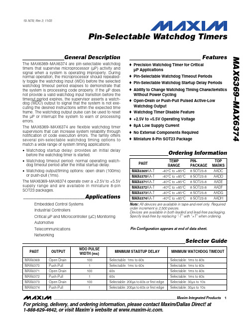
General DescriptionThe MAX6369–MAX6374 are pin-selectable watchdog timers that supervise microprocessor (µP) activity and signal when a system is operating improperly. During normal operation, the microprocessor should repeated-ly toggle the watchdog input (WDI) before the selected watchdog timeout period elapses to demonstrate that the system is processing code properly. If the µP does not provide a valid watchdog input transition before the timeout period expires, the supervisor asserts a watch-dog (WDO ) output to signal that the system is not exe-cuting the desired instructions within the expected time frame. The watchdog output pulse can be used to reset the µP or interrupt the system to warn of processing errors.The MAX6369–MAX6374 are flexible watchdog timer supervisors that can increase system reliability through notification of code execution errors. The family offers several pin-selectable watchdog timing options to match a wide range of system timing applications:•Watchdog startup delay: provides an initial delay before the watchdog timer is started.•Watchdog timeout period: normal operating watch-dog timeout period after the initial startup delay.•Watchdog output/timing options: open drain (100ms)or push-pull (1ms).The MAX6369–MAX6374 operate over a +2.5V to +5.5V supply range and are available in miniature 8-pin SOT23 packages.________________________ApplicationsEmbedded Control Systems Industrial ControllersCritical µP and Microcontroller (µC) Monitoring AutomotiveTelecommunications NetworkingFeatures♦Precision Watchdog Timer for Critical µP Applications ♦Pin-Selectable Watchdog Timeout Periods ♦Pin-Selectable Watchdog Startup Delay Periods ♦Ability to Change Watchdog Timing Characteristics Without Power Cycling ♦Open-Drain or Push-Pull Pulsed Active-Low Watchdog Output ♦Watchdog Timer Disable Feature ♦+2.5V to +5.5V Operating Voltage ♦8µA Low Supply Current♦No External Components Required ♦Miniature 8-Pin SOT23 PackageMAX6369–MAX6374Pin-Selectable Watchdog Timers19-1676; Rev 3; 11/05Ordering InformationPin Configuration appears at end of data sheet.Note:All devices are available in tape-and-reel only. Required order increment is 2,500 pieces.Devices are available in both leaded and lead-free packaging.Specify lead-free by replacing “-T” with “+T” when ordering.Selector GuideFor pricing, delivery, and ordering information,please contact Maxim/Dallas Direct!at1-888-629-4642, or visit Maxim’s website at .M A X 6369–M A X 6374Pin-Selectable Watchdog Timers 2_______________________________________________________________________________________ABSOLUTE MAXIMUM RATINGSELECTRICAL CHARACTERISTICS(V CC = +2.5V to +5.5V, SET_ = V CC or GND, T A = -40°C to +85°C, unless otherwise noted. Typical values are at T A = +25°C andStresses beyond those listed under “Absolute Maximum Ratings” may cause permanent damage to the device. These are stress ratings only, and functional operation of the device at these or any other conditions beyond those indicated in the operational sections of the specifications is not implied. Exposure to absolute maximum rating conditions for extended periods may affect device reliability.Terminal Voltage (with respect to GND)V CC .....................................................................-0.3V to +6V WDI.....................................................................-0.3V to +6V WDO (Open Drain: MAX6369/71/73).................-0.3V to +6V WDO (Push-Pull: MAX6370/72/74 .......-0.3V to (V CC + 0.3V)SET0, SET1, SET2................................-0.3V to (V CC + 0.3V)Maximum Current, Any Pin (input/output)...........................20mAContinuous Power Dissipation (T A = +70°C)SOT23-8 (derate 8.75mW/°C above +70°C)...............700mW Operating Temperature Range ...........................-40°C to +85°C Storage Temperature Range.............................-65°C to +150°C Junction Temperature......................................................+150°C Lead Temperature (soldering, 10s).................................+300°C V CC Rise or Fall Rate......................................................0.05V/µsMAX6369–MAX6374Pin-Selectable Watchdog Timers_______________________________________________________________________________________3ELECTRICAL CHARACTERISTICS (continued)M A X 6369–M A X 6374Pin-Selectable Watchdog Timers 4_______________________________________________________________________________________461081214-4010-15356085SUPPLY CURRENT vs. TEMPERATURETEMPERATURE (°C)S U P P L Y C U R R E N T (µA )Typical Operating Characteristics(Circuit of Figure 1, T A = +25°C, unless otherwise noted .)0.9970.9990.9981.0011.0001.0021.003-4010-15356085WATCHDOG TIMEOUT PERIODvs. TEMPERATUREM A X 6369/74-02TEMPERATURE (°C)N O R M A L I Z E D W A T C H D O G T I M E O U T P E R I O DELECTRICAL CHARACTERISTICS (continued)Note 2:Guaranteed by design.Note 3:In this setting the watchdog timer is inactive and startup delay ends when WDI sees its first level transition. See SelectingDevice Timing for more information.Note 4:After power-up, or a setting change, there is an internal setup time during which WDI is ignored.MAX6369–MAX6374Pin-Selectable Watchdog Timers_______________________________________________________________________________________5Pin DescriptionDetailed DescriptionThe MAX6369–MAX6374 are flexible watchdog circuits for monitoring µP activity. During normal operation, the internal timer is cleared each time the µP toggles the WDI with a valid logic transition (low to high or high to low) within the selected timeout period (t WD ). The WDO remains high as long as the input is strobed within the selected timeout period. If the input is not strobed before the timeout period expires, the watchdog output is asserted low for the watchdog output pulse width (t WDO ). The device type and the state of the three logic control pins (SET0, SET1, and SET2) determine watch-dog timing characteristics. The three basic timing varia-tions for the watchdog startup delay and the normalTable 1 for the timeout characteristics for all devices in the family):•Watchdog Startup Delay:Provides an initial delay before the watchdog timer is started.Allows time for the µP system to power up and initial-ize before assuming responsibility for normal watch-dog timer updates.Includes several fixed or pin-selectable startup delay options from 200µs to 60s, and an option to wait for the first watchdog input transition before starting the watchdog timer.M A X 6369–M A X 6374Pin-Selectable Watchdog Timers 6_______________________________________________________________________________________•Watchdog Timeout Period:Normal operating watchdog timeout period after the initial startup delay.A watchdog output pulse is asserted if a valid watch-dog input transition is not received before the timeout period elapses.Eight pin-selectable timeout period options for each device, from 30µs to 60s.Pin-selectable watchdog timer disable feature.•Watchdog Output/Timing Options:Open drain, active low with 100ms minimum watch-dog output pulse (MAX6369/MAX6371/MAX6373).Push-pull, active low with 1ms minimum watchdog output pulse (MAX6370/MAX6372/MAX6374).Each device has a watchdog startup delay that is initi-ated when the supervisor is first powered or after the user modifies any of the logic control set inputs. The watchdog timer does not begin to count down until theFigure 1. Functional Diagramcompletion of the startup delay period, and no watch-dog output pulses are asserted during the startup delay. When the startup delay expires, the watchdog begins counting its normal watchdog timeout period and waiting for WDI transitions. The startup delay allows time for the µP system to power up and fully ini-tialize before assuming responsibility for the normal watchdog timer updates. Startup delay periods vary between the different devices and may be altered by the logic control set pins. To ensure that the system generates no undesired watchdog outputs, the routine watchdog input transitions should begin before the selected minimum startup delay period has expired. The normal watchdog timeout period countdown is initi-ated when the startup delay is complete. If a valid logic transition is not recognized at WDI before the watchdog timeout period has expired, the supervisor asserts a watchdog output. Watchdog timeout periods vary between the different devices and may be altered by the logic control set pins. To ensure that the system generates no undesired watchdog outputs, the watch-dog input transitions should occur before the selected minimum watchdog timeout period has expired.The startup delay and the watchdog timeout period are determined by the states of the SET0, SET1, and SET2 pins, and by the particular device within the family. For the MAX6369 and MAX6370, the startup delay is equal to the watchdog timeout period. The startup and watchdog timeout periods are pin selectable from 1ms to 60s (minimum).For the MAX6371 and MAX6372, the startup delay is fixed at 60s and the watchdog timeout period is pin selectable from 1ms to 60s (minimum).The MAX6373/MAX6374 provide two timing variations for the startup delay and normal watchdog timeout. Five of the pin-selectable modes provide startup delays from 200µs to 60s minimum, and watchdog timeout delays from 3ms to 10s minimum. Two of the selectable modes do not initiate the watchdog timer until the device receives its first valid watchdog input transition (there is no fixed period by which the first input must be received). These two extended startup delay modesare useful for applications requiring more than 60s for system initialization.All the MAX6369–MAX6374 devices may be disabledwith the proper logic control pin setting (Table 1).Applications InformationInput Signal Considerations Watchdog timing is measured from the last WDI risingor falling edge associated with a pulse of at least 100nsin width. WDI transitions are ignored when WDO is asserted, and during the startup delay period (Figure2). Watchdog input transitions are also ignored for asetup period, t SETUP, of up to 300µs after power-up ora setting change (Figure 3).Selecting Device TimingSET2, SET1, and SET0 program the startup delay and watchdog timeout periods (Table 1). Timeout settingscan be hard wired, or they can be controlled with logicgates and modified during operation. To ensure smooth transitions, the system should strobe WDI immediately before the timing settings are changed. This minimizesthe risk of initializing a setting change too late in thetimer countdown period and generating undesired watchdog outputs. After changing the timing settings,two outcomes are possible based on WDO. If the change is made while WDO is asserted, the previous setting is allowed to finish, the characteristics of thenew setting are assumed, and the new startup phase is entered after a 300µs setup time (t SETUP) elapses. Ifthe change is made while WDO is not asserted, thenew setting is initiated immediately, and the new start-up phase is entered after the 300µs setup time elapses.MAX6369–MAX6374Pin-Selectable Watchdog Timers_______________________________________________________________________________________7 Figure 3. Setting Change TimingM A X 6369–M A X 6374Pin-Selectable Watchdog TimersSelecting 011 (SET2 = 0, SET1 = 1, SET0 = 1) disables the watchdog timer function on all devices in the family.Operation can be reenabled without powering down by changing the set inputs to the new desired setting. The device assumes the new selected timing characteris-tics and enter the startup phase after the 300µs setup time elapses (Figure 3).The MAX6373/MAX6374 offer a first-edge feature. In first-edge mode (settings 101 or 110, Table 1), the internal timer does not control the startup delay period.Instead, startup terminates when WDI sees a transition.If changing to first-edge mode while the device is oper-ating, disable mode must be entered first. It is then safe to select first-edge mode. Entering disable mode first ensures the output is unasserted when selecting first-edge mode and removes the danger of WDI being masked out.OutputThe MAX6369/MAX6371/MAX6373 have an active-low,open-drain output that provides a watchdog output pulse of 100ms. This output structure sinks current when WDO is asserted. Connect a pullup resistor from WDO to any supply voltage up to +5.5V.Select a resistor value large enough to register a logic low (see Ele ctrical Characte ristics ), and small enoughto register a logic high while supplying all input current and leakage paths connected to the WDO line. A 10k Ωpullup is sufficient in most applications. The MAX6370/MAX6372/MAX6374 have push-pull outputs that pro-vide an active-low watchdog output pulse of 1ms.When WDO deasserts, timing begins again at the beginning of the watchdog timeout period (Figure 2).Usage in Noisy EnvironmentsIf using the watchdog timer in an electrically noisy envi-ronment, a bypass capacitor of 0.1µF should be con-nected between V CC and GND as close to the device as possible, and no further away than 0.2 inches.________________Watchdog SoftwareConsiderationsTo help the watchdog timer monitor software execution more closely, set and reset the watchdog input at differ-ent points in the program, rather than pulsing the watch-dog input high-low-high or low-high-low. This technique avoids a stuck loop, in which the watchdog timer would continue to be reset inside the loop, keeping the watch-dog from timing out. Figure 4 shows an example of a flow diagram where the I/O driving the watchdog input is set high at the beginning of the program, set low at the end of every subroutine or loop, then set high again when the program returns to the beginning. If the pro-gram should hang in any subroutine, the problem would be quickly corrected, since the I/O is continually set low and the watchdog timer is allowed to time out, causing WDO to pulse.Figure 4. Watchdog Flow DiagramChip InformationTRANSISTOR COUNT: 1500PROCESS: BiCMOSPin ConfigurationMaxim cannot assume re sponsibility for use of any circuitry othe r than circuitry e ntire ly e mbodie d in a Maxim product. No circuit pate nt lice nse s are implied. Maxim reserves the right to change the circuitry and specifications without notice at any time.8_____________________Maxim Integrated Products, 120 San Gabriel Drive, Sunnyvale, CA 94086 408-737-7600©2005 Maxim Integrated ProductsPrinted USAis a registered trademark of Maxim Integrated Products, Inc.。
MAX5937LBESA+中文资料
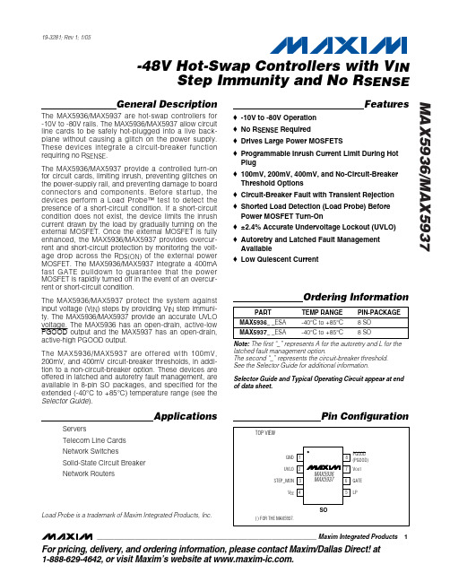
MAX5936/MAX5937-48V Hot-Swap Controllers with V INStep Immunity and No R SENSE________________________________________________________________Maxim Integrated Products 119-3281; Rev 1; 1/05For pricing, delivery, and ordering information,please contact Maxim/Dallas Direct!at 1-888-629-4642, or visit Maxim’s website at .General DescriptionThe MAX5936/MAX5937 are hot-swap controllers for -10V to -80V rails. The MAX5936/MAX5937 allow circuit line cards to be safely hot-plugged into a live back-plane without causing a glitch on the power supply.These devices integrate a circuit-breaker function requiring no R SENSE .The MAX5936/MAX5937 provide a controlled turn-on for circuit cards, limiting inrush, preventing glitches on the power-supply rail, and preventing damage to board connectors and components. Before startup, the devices perform a Load Probe™ test to detect the presence of a short-circuit condition. If a short-circuit condition does not exist, the device limits the inrush current drawn by the load by gradually turning on the external MOSFET. Once the external MOSFET is fully enhanced, the MAX5936/MAX5937 provides overcur-rent and short-circuit protection by monitoring the volt-age drop across the R DS(ON)of the external power MOSFET. The MAX5936/MAX5937 integrate a 400mA fast G ATE pulldown to guarantee that the power MOSFET is rapidly turned off in the event of an overcur-rent or short-circuit condition.The MAX5936/MAX5937 protect the system against input voltage (V IN ) steps by providing V IN step immuni-ty. The MAX5936/MAX5937 provide an accurate UVLO voltage. The MAX5936 has an open-drain, active-low PGOOD output and the MAX5937 has an open-drain,active-high PGOOD output.The MAX5936/MAX5937 are offered with 100mV,200mV, and 400mV circuit-breaker thresholds, in addi-tion to a non-circuit-breaker option. These devices are offered in latched and autoretry fault management, are available in 8-pin SO packages, and specified for the extended (-40°C to +85°C) temperature range (see the Selector Guide ).ApplicationsServersTelecom Line Cards Network Switches Solid-State Circuit Breaker Network RoutersFeatures♦-10V to -80V Operation ♦No R SENSE Required♦Drives Large Power MOSFETS♦Programmable Inrush Current Limit During Hot Plug ♦100mV, 200mV, 400mV, and No-Circuit-Breaker Threshold Options ♦Circuit-Breaker Fault with Transient Rejection ♦Shorted Load Detection (Load Probe) Before Power MOSFET Turn-On ♦±2.4% Accurate Undervoltage Lockout (UVLO)♦Autoretry and Latched Fault Management Available ♦Low Quiescent CurrentPin ConfigurationLoad Probe is a trademark of Maxim Integrated Products, Inc.Ordering InformationNote:The first “_” represents A for the autoretry and L for the latched fault management option.The second “_” represents the circuit-breaker threshold. See the Selector Guide for additional information.Selector Guide and Typical Operating Circuit appear at end of data sheet.M A X 5936/M A X 5937-48V Hot-Swap Controllers with V IN Step Immunity and No R SENSE 2_______________________________________________________________________________________ABSOLUTE MAXIMUM RATINGSStresses beyond those listed under “Absolute Maximum Ratings” may cause permanent damage to the device. These are stress ratings only, and functional operation of the device at these or any other conditions beyond those indicated in the operational sections of the specifications is not implied. Exposure to absolute maximum rating conditions for extended periods may affect device reliability.V EE , V OUT , PGOOD (PGOOD ), LP,STEP_MON to GND............................................+0.3V to -85V PGOOD (PGOOD ) to V OUT ....................................-0.3V to +85V PGOOD (PGOOD ), LP, STEP_MON to V EE ............-0.3V to +85V GATE to V EE ...........................................................-0.3V to +20V UVLO to V EE .............................................................-0.3V to +6V Input CurrentLP (internally, duty-cycle limited).........................................1A PGOOD (PGOOD ) (continuous).....................................80mAGATE (during 15V clamp, continuous)...........................30mA GATE (during 2V clamp, continuous).............................50mA GATE (during gate pulldown, continuous)......................50mA Continuous Power Dissipation (T A = +70°C)8-Pin SO (derate 5.9mW/°C above +70°C)..................471mW Operating Temperature Range ...........................-40°C to +85°C Junction Temperature .....................................................+150°C Storage Temperature Range ............................-65°C to +150°C Lead Temperature (soldering, 10s) ................................+300°CELECTRICAL CHARACTERISTICS(V= -10V to -80V, V = GND - V , V =V , R = 200Ω, UVLO open, T = -40°C to +85°C, unless otherwise noted.MAX5936/MAX5937-48V Hot-Swap Controllers with V INStep Immunity and No R SENSEELECTRICAL CHARACTERISTICS (continued)M A X 5936/M A X 5937-48V Hot-Swap Controllers with V IN Step Immunity and No R SENSE 4_______________________________________________________________________________________Note 2:All limits are 100% tested at +25°C and +85°C. Limits at -40°C and -10°C are guaranteed by characterization.Note 3:Delay time from a valid on-condition until the load probe test begins.Note 4:V EE or UVLO voltages below V UVLO,F or V UVLO_REF,F , respectively, are ignored during this time.Note 5:The time (V OUT - V EE ) > V SC + overdrive until (V GATE - V EE ) drops to approximately 90% of its initial high value.Note 6:The time when the PGOOD (PGOOD ) condition is met until the PGOOD (PGOOD ) signal is asserted.ELECTRICAL CHARACTERISTICS (continued)MAX5936/MAX5937-48V Hot-Swap Controllers with V INStep Immunity and No R SENSE_______________________________________________________________________________________5SUPPLY CURRENT vs. INPUT VOLTAGEM A Z 5936 t o c 01INPUT VOLTAGE (V)S U P P L Y C U R R E N T (m A )7060405030200.20.40.60.81.01.21.41.61.82.001080SUPPLY CURRENT vs. TEMPERATURETEMPERATURE (°C)S U P P L Y C U R R E N T (m A )603510-150.20.40.60.81.01.20-4085GATE-DRIVE VOLTAGE vs. INPUT VOLTAGEM A X 536 t o c 03INPUT VOLTAGE (V)G A T E -D R I V E V O L T A G E (V )7060405030206.57.07.58.08.59.09.510.010.56.01080GATE PULLDOWN CURRENTvs. GATE VOLTAGEM A X 5936 t o c 04V GATE (V)G A T E P U L L D O W N C U R R E N T (m A )986723451501001502002503003504004505000010RETRY TIME vs. TEMPERATURETEMPERATURE (°C)R E T R Y T I M E (s )603510-153.13.23.33.43.53.63.73.83.94.03.0-4085STARTUP WAVEFORMMAX5936 toc0640ms/divV IN 50V/div V GATE 10V/div V OUT 50V/div I IN 2A/divV PGOOD 50V/div MAX5936_A CIRCUIT-BREAKER EVENTMAX5936 toc071ms/divV GATE 10V/divV OUT 50V/divI IN 2A/divV PGOOD 50V/div Typical Operating Characteristics(V EE = -48V, GND = 0V, V IN = GND - V EE , all voltages are referenced to V EE , T A = +25°C, unless otherwise noted.)M A X 5936/M A X 5937-48V Hot-Swap Controllers with V IN Step Immunity and No R SENSE 6_______________________________________________________________________________________MAX5936_A SHORT-CIRCUIT EVENTMAX5936 toc08400ns/divV GATE 10V/divV OUT 50V/div I IN10A/divV PGOOD 50V/divNORMALIZED CIRCUIT-BREAKER THRESHOLD vs. TEMPERATUREM A X 5936 t o c 09TEMPERATURE (°C)N O R M A L I Z E D C I R C U I T -B R E A K E R T H R E S H O L D (%)603510-150.60.81.01.21.41.60.4-4085V OUT SLEW RATE vs. TEMPERATURETEMPERATURE (°C)S L E W R A T E (V /m s )603510-155.56.0 6.57.07.58.08.59.09.510.05.0-4085MAX5936_A INPUT VOLTAGE STEP EVENT (NO FAULT)4ms/divGATE OUT IN V PGOOD IN R LOAD = 75ΩMAX5936_A INPUT VOLTAGESTEP EVENT (FAULT)4ms/divGATE OUT IN V PGOODIN R LOAD = 75ΩGATE TO V EE CLAMP VOLTAGEAT POWER OFFI SINK (mA)G A T E C L A M P I N G V O L T A G E (V )181614121086420.51.01.52.02.53.00020GATE TO V EE CLAMP VOLTAGE MOSFET FULLY ENHANCEDI SINK (mA)G A T E C L A M P I N G V O L T A G E (V )1816121446810291011121314151617188020Typical Operating Characteristics (continued)(V EE = -48V, GND = 0V, V IN = GND - V EE , all voltages are referenced to V EE , T A = +25°C, unless otherwise noted.)MAX5936/MAX5937-48V Hot-Swap Controllers with V INStep Immunity and No R SENSE_______________________________________________________________________________________7Detailed DescriptionThe MAX5936/MAX5937 hot-swap controllers incorpo-rate overcurrent fault management and are intended for negative-supply-rail applications. The MAX5936/MAX5937 eliminate the need for an external R SENSE and include V IN input-step protection and load probe,which prevents powering up into a shorted load. They are intended for negative 48V telecom power systems where low cost, flexibility, multifault management, and compact size are required. The MAX5936/MAX5937 are ideal for the widest range of systems from those requiring low current with small MOSFETs to high-current systems requiring large power MOSFETs and low on-resistance.The MAX5936/MAX5937 control an external n-channel power MOSFET placed in the negative supply path of an external load. When no power is applied, the GATE output of the MAX5936/MAX5937 clamps the V GS of the MOSFET to 2V, keeping the MOSFET turned off. When power is applied to the MAX5936/MAX5937, the 2Vdown device pulling G ATE to V EE and the V GS of the MOSFET to 0V. As shown in Figure 2, this transition enables the MAX5936/MAX5937 to keep the power MOSFET continually off during the board insertion phase when the circuit board first makes contact with the backplane. Without this clamp, the GATE output of a powered-down controller would be floating and the MOSFET reverse transfer capacitance (gate-to-drain)would pull up and turn on the MOSFET gate when the MOSFET drain is rapidly pulled up by the V IN step dur-ing backplane contact. The MAX5936/MAX5937 G ATE clamp can overcome the gate-to-drain capacitance of large power MOSFETs with added slew-rate control (C SLEW ) capacitors while eliminating the need for addi-tional gate-to-source capacitance. The MAX5936/MAX5937 will keep the MOSFET off indefinitely if the supply voltage is below the user-set UVLO threshold or if a short circuit is detected in the load connected to the drain of the power MOSFET.M A X 5936/M A X 5937-48V Hot-Swap Controllers with V IN Step Immunity and No R SENSE 8_______________________________________________________________________________________The MAX5936/MAX5937 conduct a load-probe test after contact transients from the hot plug-in have settled. This follows the MAX5936/MAX5937 power-up (when the UVLO condition has been met for 220ms (t LP )) and prior to the turn-on of the power MOSFET. This test pulls a user-programmable current through the load (1A, max)for up to 220ms and tests for a voltage of 200mV across the load at V OUT . This current is set by an external resis-tor, R LP , between V OUT and LP (Figure 14). When the voltage across the load exceeds 200mV, the test is trun-cated and the GATE turn-on sequence is started. If at the end of the 220ms test period the voltage across the load has not reached 200mV, the load is assumed to be short-ed and the current to the load from the LP pin is shut off.The MAX5936A_/MAX5937A_ will timeout for 16 x t LP then retry the load-probe test. The MAX5936L_/MAX5937L_ will latch the fault condition indefinitely untilthe UVLO is brought below 1.125V for 1.5ms or the power is recycled. See the Applications Information section for recommendations on selecting R LP to set the current level.Upon successful completion of the load-probe test, the MAX5936/MAX5937 enter the power-up GATE cycle and begin ramping the G ATE voltage with a 52µA current source. This current source is restricted if V OUT begins to ramp down faster than the default 9V/ms slew rate.Charging up G ATE enhances the power MOSFET in a controlled manner and ramping V OUT at a user-settable rate controls the inrush current from the backplane. The MAX5936/MAX5937 continue to charge up the G ATE until one of two events occurs: a normal power-up GATE cycle is completed or a power-up to fault management is detected (see the GATE Cycles section in Appendix A ).Figure 1. Functional Block DiagramMAX5936/MAX5937-48V Hot-Swap Controllers with V INStep Immunity and No R SENSE_______________________________________________________________________________________9In a normal power-up GATE cycle, the voltage at V OUT (referenced to V EE ) ramps to below 72% of the circuit-breaker threshold voltage, V CB . At this time, the remaining GATE voltage is rapidly pulled up to full enhancement.PGOOD is asserted 1.26ms after GATE is fully enhanced (see Figure 4). If the voltage at V OUT remains above 72%of the V CB (when GATE reaches 90% of full enhance-ment), then a power-up to fault management fault has occurred (see Figure 5). GATE is rapidly pulled to V EE ,turning off the power MOSFET and disconnecting the load. PGOOD remains deasserted and the MAX5936/MAX5937 enter the fault management mode.When the power MOSFET is fully enhanced, the MAX5936/MAX5937 monitor the drain voltage (V OUT ) for circuit-breaker and short-circuit faults. The MAX5936/MAX5937 make use of the power MOSFET’s R DS(ON) as the current-sense resistance to detect excessive current through the load. The short-circuit threshold voltage,V SC , is twice V CB (V SC = 2 x V CB ) and is available in 100mV, 200mV, and 400mV thresholds. V CB and V SC are temperature-compensated (increasing with tempera-ture) to track the normalized temperature coefficient of R DS(ON) for typical power MOSFETs.When the load current is increased during full enhance-ment, this causes V OUT to exceed V CB but remains less than V SC , and starts the 1.2ms circuit-breaker glitch rejection timer. At the end of the glitch rejection period,if V OUT still exceeds V CB , the G ATE is immediately pulled to V EE (330ns), PGOOD (PGOOD ) is deasserted,and the part enters fault management. Alternatively,during full enhancement when V OUT exceeds V SC ,there is no glitch rejection timer. G ATE is immediately pulled to V EE , PG OOD is deasserted, and the part enters fault management.Figure 3. Load Probe Test During Initial Power-Up40ms/divV 20V/divV 20V/divV 20V/divALL VOLTAGESREFERENCED TO GND Figure 2. GATE Voltage Clamp During Power-Up 4ms/divC IN = 100µFFigure 4. MAX5936 Normal Condition 40ms/divFigure 5. MAX5936 Startup in Fault Condition40ms/divM A X 5936/M A X 5937-48V Hot-Swap Controllers with V IN Step Immunity and No R SENSE10______________________________________________________________________________________The V IN step immunity provides a means for transition-ing through a large step increase in V IN with minimal backplane inrush current and without shutting down the load. Without V IN step immunity (when the power MOSFET is fully enhanced), a step increase in V IN will result in a high inrush current and a large step in V OUT ,which can trip the circuit breaker. With V IN step immu-nity, the STEP_MON input detects the step before a short circuit is detected at V OUT and alters the MAX5936/MAX5937 response to V OUT exceeding V SC due to the step. The 1.25V voltage threshold at STEP_MON and a 10µA current source at STEP_MON allow the user to set the sensitivity of the step detection with an external resistor to V EE . A capacitor is placed between GND and the STEP_MON input, which, in con-junction with the resistor, sets the STEP_MON time con-stant. When a step is detected by the STEP_MON input to rise above its threshold (STEP TH ), the overcurrent fault management is blocked and remains blocked as long as STEP TH is exceeded. When STEP TH is exceed-ed, the MAX5936/MAX5937 take no action until V OUT rises above V SC or above V CB for the 1.2ms circuit-breaker glitch rejection period. When either of these conditions occurs, a step G ATE cycle begins and the GATE is immediately brought to V EE , which turns off the power MOSFET to minimize the resulting inrush current surge from the backplane and PGOOD remains assert-ed. GATE is held at V EE for 350µs, and after about 1ms,begins to ramp up thereby enhancing the power MOSFET in a controlled manner as in the power-up G ATE cycle. This provides a controlled inrush current to charge the load capacitance to the new supply volt-age (see the GATE Cycles section in Appendix A ).As in the case of the power-up G ATE cycle, if V OUT drops to less than 72% of the programmed V CB , inde-pendent of the state of STEP_MON, the G ATE voltageis rapidly pulled to full enhancement. PGOOD remains asserted throughout the step. Otherwise, if the STEP_MON input has decayed below its threshold but V OUT remains above 72% of the programmed V CB (when G ATE reaches 90% of full enhancement), (a step-to-fault management fault has occurred). GATE is rapidly pulled to V EE , turning off the power MOSFET and disconnecting the load, PG OOD (PGOOD ) is deasserted, and the MAX5936/MAX5937 enter the fault management mode.Fault ManagementFault management can be triggered by the following conditions:•V OUT exceeds 72% of V CB during G ATE ramp at 90% of full enhancement,•V OUT exceeds the V CB for longer than 1.2ms during full enhancement,•V OUT exceeds the V SC during full enhancement, and •Load-probe test fails.Once in the fault management mode, GATE will always be pulled to V EE to turn off the external MOSFET and PG OOD (PGOOD ) will always be deasserted. The MAX5936A_/MAX5937A_ have automatic retry following a fault while the MAX5936L_/MAX5937L remain latched in the fault condition.Autoretry Fault Management(MAX5936A_/MAX5937A_)If the MAX5936A_/MAX5937A_entered fault management due to circuit-breaker and short-circuit faults, the autoretry timer starts immediately. The timer times out in 3.5s (typ) and at the end of the timeout, the sequencer initiates a load-probe test. If this is successful, it starts a normal power-up GATE cycle.Figure 6. MAX5936 Response to a Step Input (V OUT < 0.74V CB )2ms/divC LOAD = 100µF R LOAD = 100ΩFigure 7. MAX5936 Response to a Step Input (V OUT > 0.74V CB )4ms/div40V 20VC LOAD = 100µF R LOAD = 20ΩMAX5936/MAX5937-48V Hot-Swap Controllers with V INStep Immunity and No R SENSE______________________________________________________________________________________11Latched Fault Management (MAX5936L_/MAX5937L_)When the MAX5936L_/MAX5937L_ enter fault manage-ment, they remain in this condition indefinitely until the power is recycled or until UVLO is brought below 1.125V for 1.5ms (typ) (when the short-circuit or circuit-breaker fault has cleared, the sequencer initiates a load-probe test). If this is successful, it starts a normal power-up GATE cycle. A manual reset circuit (Figure 8)can be used to clear the latch.Circuit-Breaker ThresholdsThe MAX5936/MAX5937 are available with 100mV,200mV, and 400mV circuit-breaker thresholds. The short-circuit voltage threshold (V SC ) is twice the circuit-breaker threshold voltage (V CB ). In the MAX5936/MAX5937, V CB and V SC are temperature-compensated (increasing with temperature) to track the normalized temperature gradient of typical power MOSFETs.The proper circuit-breaker threshold for an application depends on the R DS(ON) of the external power MOSFET and the maximum current the load is expected to draw.To avoid false fault indication and dropping of the load,the designer must take into account the load response to voltage ripples and noise from the backplane power supply, as well as switching currents in the downstream DC-DC converter that is loading the circuit. While the circuit-breaker threshold has glitch rejection that ignores ripples and noise lasting less than 1.2ms, the short-circuit detection is designed to respond very quickly (less than 330ns) to a short circuit. V SC and V CB must be selected from the three available rangeswith an adequate margin to cover all possible ripples,noise, and system current transients.The short-circuit and circuit-breaker voltages are sensed at V OUT , which is the drain of the power MOSFET. The R DS(ON)of the MOSFET is the current-sense resis-tance, so the total current through the load and load capacitance is the drain current of the power MOSFET.Accordingly, the voltage at V OUT as a function of MOSFET drain current is:V OUT = I D,MOSFET x R DS(ON)The temperature compensation of the MAX5936/MAX5937 is designed to track the R DS(ON) of the typi-cal power MOSFET. Figure 9 shows the typical normal-ized tempco of the circuit-breaker threshold along with the normalized tempco of R DS(ON) for two typical power MOSFETS. When determining the circuit-breaker threshold in an application, go to the data sheet of the power MOSFET and locate the manufacturer’s maxi-mum R DS(ON)at +25°C with a V GS of 10V. Next, find the figure presenting the tempco of normalized R DS(ON)or on-resistance vs. temperature. Because this curve is in normalized units typically with a value of 1 at +25°C,it is possible to multiply the curve by the drain voltage at +25°C and convert the curve to drain voltage. Now compare this curve to that of the MAX5936/MAX5937 normalized tempco of the circuit-breaker threshold to make a determination of the tracking error in mV between the power MOSFET [I D,MOSFET x R DS(ON)]and the MAX5936/MAX5937 over the application’s operating temperature range. If the tempco of the power MOSFET is greater than that of the MAX5936/MAX5937, then additional margin will be required in selecting the circuit-breaker and short-circuit voltages at higher temperatures as compared to +25°C. When dissipation in the power MOSFET is expected to lead to local temperature elevation relative to ambient condi-tions, then it becomes imperative that the MAX5936/MAX5937 be located as close as possible to the power MOSFET. The marginal effect of temperature differ-ences on circuit-breaker and short-circuit voltages can be estimated from a comparative plot such as Figure 9.MAX5936LN and MAX5937LNThe MAX5936LN and MAX5937LN do not have circuit-breaker and short-circuit thresholds and these faults are ignored. For these devices PG OOD (PGOOD )asserts 1.26ms after G ATE has ramped to 90% of full enhancement. The step detection function of the MAX5936LN and MAX5937LN responds to V IN and V OUT steps with the same voltage thresholds as the MAX5936_C and MAX5937_C.Figure 8. Resetting MAX5936L/MAX5937L after a Fault Condition Using a Push-Button SwitchM A X 5936/M A X 5937-48V Hot-Swap Controllers with V IN Step Immunity and No R SENSE12______________________________________________________________________________________PGOOD (PGOOD ) Open-Drain OutputThe power-good outputs, PG OOD (PGOOD ), are open drain and are referenced to V OUT . They assert and latch if V OUT ramps below 72% of V CB , and with the built-in delay this occurs 1.26ms after the external MOSFET becomes fully enhanced. PG OOD (PGOOD ) deasserts any time the part enters fault management. PG OOD (PGOOD ) has a delayed response to UVLO. The GATE goes to V EE when UVLO is brought below 1.125V for 1.5ms. This turns off the power MOSFET and allows V OUT to rise depending on the RC time constant of the load. PG OOD (PGOOD ), in this situation, deasserts when V OUT rises above V CB for more than 1.4ms or above V SC , whichever occurs first (see Figure 12b).Due to the open-drain driver, PG OOD (PGOOD )requires an external pullup resistor to GND. Due to this external pullup, PG OOD will not follow positive V IN steps as well as if it were driven by an active pullup. As a result, when PG OOD (PGOOD) is asserted high, an apparent negative glitch appears at PGOOD (PGOOD )during a positive V IN step. This negative glitch is a result of the RC time constant of the external resistor and the PGOOD pin capacitance lagging the V IN step.It is not due to switching of the internal logic. To mini-mize this negative transient, it may be necessary to increase the pullup current and/or to add a small amount of capacitance from PGOOD (PGOOD ) to GND to compensate for the pin capacitance.WARNING:For the MAX5936_N/MAX5937_N, PGOOD (PGOOD ) asserts 1.26ms after the power MOSFET is fully enhanced, independent of V OUT . Once the MOSFET is fully enhanced and UVLO is pulled below its respective threshold, G ATE pulls to V EE to turn off the power MOSFET and disconnect the load. When UVLO is cycled low, PG OOD (PGOOD ) is deasserted. In sum-mary, once the MOSFET is fully enhanced, the MAX5936_N/ MAX5937_N ignore V OUT and deassert PG OOD (PGOOD ) when UVLO goes low or when the power to the MAX5936_N/ MAX5937_N is fully recy-cled.Undervoltage Lockout (UVLO)UVLO provides an accurate means to set the turn-on volt-age level for the MAX5936/MAX5937. Use a resistor-divider network from G ND to V EE to set the desired turn-on voltage (Figure 11). UVLO has hysteresis with a rising threshold of 1.25V and a falling threshold of 1.125V.A startup delay of 220ms allows contacts and voltages to settle prior to initiating the startup sequence (Figure 12a).Figure 9. MAX5936/MAX5937 Normalized Circuit-Breaker Threshold (V CB )Figure 10. Circuit-Breaker Voltage Margin for High and Low Tempco Power MOSFETSMAX5936/MAX5937-48V Hot-Swap Controllers with V INStep Immunity and No R SENSE______________________________________________________________________________________13This startup delay is from a valid UVLO condition until the start of the load-probe test. There is glitch rejection on UVLO going low, which requires that V UVLO remains below its falling threshold for 1.5ms to turn off the part (Figure 12b). Use the following formula to calculate the MAX5936/MAX59337 turn-on voltage:Where V ON is the desired turn-on voltage of theMAX5936/MAX5937 and V UVLO_REF,R is the 1.25V UVLO rising threshold.Output Voltage (V OUT )Slew-Rate ControlThe V OUT slew rate controls the inrush current required to charge the load capacitor. The MAX5936/MAX5937have a default internal slew rate set for 9V/ms. The inter-nal circuit establishing this slew rate accommodates up to about 1000pF of reverse transfer capacitance (miller capacitance) in the external power MOSFET without effecting the default slew rate. Using the default slew rate, the inrush current required to charge the load capacitance is given by:I INRUSH (mA) = C LOAD (µF) x SR (V/ms)where SR = 9V/ms (default, typ).Applications InformationSelecting Resistor and Capacitorfor Step MonitorWhen a positive V IN step or ramp occurs, the V IN increase results in a voltage rise at both STEP_MON and V OUT relative to V EE . When the voltage at STEP_MON is above STEP TH the MAX5936/MAX5937block short-circuit and circuit-breaker faults. During this STEP_MON high condition, if V OUT rises above V SC , the MAX5936/MAX5937 immediately and very rapidly pull GATE to V EE . This turns off the power MOSFET to avoid inrush current spiking. G ATE is held low for 350µs.About 1ms after the start of G ATE pulldown, the MAX5936/MAX5937 begin to ramp GATE up to turn on the MOSFET in a controlled manner, which results in ramping V OUT down to the new supply level (see the GATE Cycles section in Appendix A ).Figure 11. Setting the MAX5936/MAX5937 Turn-On VoltageFigure 12. UVLO Timing Diagram。
MAX6339LUT-T中文资料

General DescriptionThe MAX6339 is a precision quad voltage monitor with microprocessor (µP) supervisory reset timing. The device can monitor up to four system supply voltages without any external components and asserts a single reset if any supply voltage drops below its preset threshold. The device significantly reduces system size and component count while improving reliability compared to separate ICs or discrete components.A variety of factory-trimmed threshold voltages are avail-able to accommodate different supply voltages and toler-ances with minimal external component requirements.The selection includes internally fixed options for monitor-ing +5.0V, +3.3V, +3.0V, +2.5V, +1.8V, and -5.0V sup-plies with -5% and/or -10% tolerances. The device is also available with one or two user-adjustable threshold options if non-standard thresholds are desired (use exter-nal resistor-divider network).The quad monitor provides a single active-low reset out-put that is asserted when any monitored input is below its associated threshold. The output is open drain with a weak internal pullup (10µA) to IN2. Reset remains low for a reset timeout period (140ms min) after all voltages are above the selected thresholds. The output is valid as long as either the IN1 or IN2 input voltage remains > 1V.The MAX6339 is available in a small 6-pin SOT23 pack-age and operates over the extended (-40°C to +85°C)temperature range.________________________ApplicationsTelecommunications High-End PrintersDesktop and Network Computers Data Storage Equipment Networking Equipment Industrial Equipment Set-Top BoxesFeatures♦Monitors Four Power-Supply Voltages♦Precision Factory-Set Reset Threshold Options for +5.0V, +3.3V, +3.0, +2.5V, +1.8V, and -5.0V Supplies ♦User-Adjustable Voltage Monitoring Threshold Options ♦Low 55µA Supply Current♦Open-Drain RESET Output with 10µA Internal Pullup ♦140ms (min) Reset Timeout Period ♦RESET Valid to IN1 = 1V or IN2 = 1V♦Immune to Short Monitored Supply Transients ♦No External Components Required ♦Guaranteed from -40°C to +85°C ♦Small 6-Pin SOT23 PackageMAX6339Quad Voltage µP Supervisory Circuitin SOT Package________________________________________________________________Maxim Integrated Products 119-1756; Rev 3; 12/05Ordering Information*Insert the desired letter from the Selector Guide into the blank to complete the part number. There is a 2500 piece minimum order increment requirement on the SOT package and these devices are available in tape-and-reel only.Devices are available in both leaded and lead-free packaging.Specify lead-free by replacing “-T” with “+T” when ordering.Pin Configuration appears at end of data sheet.Typical Operating CircuitFor pricing, delivery, and ordering information,please contact Maxim/Dallas Direct!at 1-888-629-4642, or visit Maxim’s website at .M A X 6339Quad Voltage µP Supervisory Circuit in SOT Package 2_______________________________________________________________________________________ABSOLUTE MAXIMUM RATINGSStresses beyond those listed under “Absolute Maximum Ratings” may cause permanent damage to the device. These are stress ratings only, and functional operation of the device at these or any other conditions beyond those indicated in the operational sections of the specifications is not implied. Exposure to absolute maximum rating conditions for extended periods may affect device reliability.Terminal Voltage (with respect to GND)Input Voltages (IN_ ) (except -5V)............................-0.3V to +6V RESET .......................................................................-0.3V to +6V Input Voltage (-5V Input)..........................................-6V to +0.3V Continuous RESET Current.................................................20mA Continuous Power Dissipation (T A = +70°C)6-pin SOT23 (derate 8.7mW/°C above +70°C).........695.7mWOperating Temperature Range ...........................-40°C to +85°C Storage Temperature Range.............................-65°C to +150°C Junction Temperature......................................................+150°C Lead Temperature (soldering, 10s).................................+300°CELECTRICAL CHARACTERISTICS(V = +1V to +5.5V, T = -40°C to +85°C, unless otherwise noted. Typical values are at V = +3.0V to +3.3V, T = +25°C, unlessMAX6339Quad Voltage µP Supervisory Circuitin SOT Package_______________________________________________________________________________________3ELECTRICAL CHARACTERISTICS (continued)(V IN2= +1V to +5.5V, T A = -40°C to +85°C, unless otherwise noted. Typical values are at V IN2= +3.0V to +3.3V, T A = +25°C, unless otherwise noted.) (Note 1)Note 1:100% production tested at T A = +25°C. Limits over temperature guaranteed by design.Note 2:The device is powered from input IN2.Note 3:The RESET output is guaranteed to be in the correct state for IN1 or IN2 down to 1V.Note 4:Monitored voltage (+3.3V, +3.0V) is also the device power supply. Supply current splits as follows: 25µA for the resistor- divider (for the monitored voltage) and 30µA for other circuits.3550454055606570758085-40-2020406080I IN2 INPUT CURRENT vs. TEMPERATURETEMPERATURE (°C)I I N 2 I N P U T C U R R E N T (µA )50605570658075853.04.03.54.55.05.5I IN2 INPUT CURRENT vs. I IN2 VOLTAGEM A X 6339t o c 02INPUT VOLTAGE (V)I I N 2 I N P U T C U R R E N T (µA )-0.30-0.15-0.20-0.25-0.10-0.500.050.100.15-40-2020406080NORMALIZED THRESHOLD ERRORvs. TEMPERATURETEMPERATURE (°C)N O R M A L I Z E D T H R E S H O L D E R R O R (%)Typical Operating Characteristics(V IN2= +3.0V, T A = +25°C)Pin DescriptionM A X 6339Quad Voltage µP Supervisory Circuit in SOT Package Typical Operating Characteristics (continued)(VIN2= +3.0V, T A = +25°C)180190185195200205210215-40-2020406080RESET TIMEOUT DELAY vs. TEMPERATUREM A X 6339t o c 07TEMPERATURE (°C)R E S E T T I M E O U T D E L A Y (m s )RESET 2V/divIN_2V/div200ms/divRESET TIMEOUT DELAYM A X 6339t o c 082V/div201030607050408002003004005001006007008009001000MAXIMUM IN_ TRANSIENT DURATION vs. RESET THRESHOLD OVERDRIVERESET THRESHOLD OVERDRIVE (mV)M A X I M U M I N _ T R A N S I E N T D U R A T I O N (µs )201030607050408002003004005001006007008009001000RESET DELAY vs. RESET THRESHOLDOVERDRIVE (IN_ decreasing)M A X 6339t o c 05RESET THRESHOLD OVERDRIVE (mV)R E S E T D E L A Y (µs )RESET 2V/divIN_100mV/div10µs/divRESET PULLUP AND PULLDOWNRESPONSE (C L = 47pF)M A X 6339t o c 06MAX6339Quad Voltage µP Supervisory Circuitin SOT Package_______________________________________________________________________________________5Detailed DescriptionThe MAX6339 is a very small, low-power, quad voltage µP supervisory circuit designed to maintain system integrity in multi-supply systems (Figure 1). The device offers several internally trimmed undervoltage threshold options that minimize or eliminate the need for external components. Preset voltage monitoring options for +5.0V, +3.3V, +3.0V, +2.5V, +1.8V, and -5.0V make it ideal for telecommunications, desktop and notebook computers, high-end printers, data storage equipment,and networking equipment applications.The quad monitor/reset includes an accurate bandgap reference, four precision comparators, and a series of internal trimmed resistor-divider networks to set the fac-tory-fixed reset threshold options. The resistor networks scale the specified IN_ reset voltages to match the internal bandgap reference/comparator voltage. User-adjustable threshold options bypass the internal resis-tor networks and connect directly to one of the comparator inputs (an external resistor-divider network is required for threshold matching). All threshold volt-age options, fixed and adjustable, are indicated through a single-letter code in the product number (see the Selector Guide ).Each of the internal comparators has a typical hystere-sis of 0.3% with respect to its reset threshold. This built-in hysteresis improves the monitor’s immunity to ambient noise without significantly reducing threshold accuracy when an input sits at its specified reset volt-age. The MAX6339 is also designed to ignore short IN_transients. See the Typical Operating Characteristics for a glitch immunity graph.Applications InformationReset OutputThe MAX6339 RESET output is asserted low when any of the monitored IN_ voltages drop below its specified reset threshold (or above for -5V option) and remain low for the reset timeout period (140ms minimum) after all inputs exceed their thresholds (Figure 2). The output is open drain with a weak internal pullup to the moni-tored IN2 supply (10µA typ). For many applications no external pullup resistor is required to interface with other logic devices. An external pullup resistor to any voltage from 0 to +5.5V can overdrive the internal pullup if interfacing to different logic supply voltages (Figure 3). Internal circuitry prevents reverse current flow from the external pullup voltage to IN2.The MAX6339 is normally powered from the monitored IN2 supply when all input voltages are above their specified thresholds. When any supply drops below itsthreshold, the reset output is asserted and guaranteed to remain low while either IN1 or IN2 is above +1.0V.User-Adjustable ThresholdsThe MAX6339 offers several monitor options with user-adjustable reset thresholds. The threshold voltage at each adjustable IN_ input is typically 1.23V. To monitor a voltage > 1.23V, connect a resistor-divider network to the circuit as shown in Figure 4.V INTH = 1.23V x (R1 + R2) / R2or, solved in terms of R1:R1 = R2 ((VI NTH / 1.23V) - 1)Because the MAX6339 has a guaranteed input current of ±0.1µA on its adjustable inputs, resistor values up to 100k Ωcan be used for R2 with < 1% error.Unused InputsIf some monitor inputs are to be unused, they must be tied to a supply voltage greater in magnitude than their specified threshold voltages. For unused IN3 or IN4options with positive thresholds (fixed or adjustable),the inputs can be connected directly to the IN2 supply.For unused IN4 options with negative thresholds, the input must be tied to a more negative supply. The IN2input must always be used for normal operation (device power-supply pin). Unused pins cannot be connected to ground or allowed to float.Negative Voltage Monitoring Beyond -5VThe MAX6339 is offered with options to monitor -5V sup-plies with internally fixed thresholds. To monitor supplies more negative than -5V, a low-impedance resistor-divider network can be used external to the MAX6339 as shown in Figure 5. The current through the external resis-tor-divider should be greater than the input current for the -5V monitor options. For an input monitor current error of < 1%, the resistor-divider current should ≥ 2mA (for I IN4= 20µA max). Set R2 = 2.5k Ω. Calculate R1based on the desired V IN_reset threshold voltage, using the following formula:R1 = R2 ✕[(V INTH / V TH ) -1]where R2 ≤2.49k Ω, V INTH = desired threshold voltage and V TH is the internal threshold voltage.M A X 6339Quad Voltage µP Supervisory Circuit in SOT Package 6_______________________________________________________________________________________Figure 1. Functional DiagramMAX6339Quad Voltage µP Supervisory Circuitin SOT Package_______________________________________________________________________________________7For -V IN = -12V nominal, VI NTH = -11.1V, V TH = -4.63V,and R2 = 2.49k Ω,R1 = 2.49k Ω✕[(-11.1 / -4.63) -1]R1 = 3.48k ΩPower-Supply Bypassing and GroundingThe MAX6339 is normally powered from the monitored IN2 supply input. All monitor inputs are immune to short supply transients. If higher immunity is desired in noisy applications, connect 0.1µF bypass capacitors from the IN2 input to ground. Additionally, capacitance can be added to IN1, IN3, and IN4 to increase their noise immunity.Chip InformationTRANSISTOR COUNT: 896PROCESS: BiCMOSFigure 4. Setting the Auxiliary MonitorM A X 6339Quad Voltage µP Supervisory Circuit in SOT Package 8_______________________________________________________________________________________Maxim cannot assume responsibility for use of any circuitry other than circuitry entirely embodied in a Maxim product. No circuit patent licenses are implied. Maxim reserves the right to change the circuitry and specifications without notice at any time.Maxim Integrated Products, 120 San Gabriel Drive, Sunnyvale, CA 94086 408-737-7600_____________________9©2005 Maxim Integrated Productsis a registered trademark of Maxim Integrated Products, Inc.6L S O T .E P SMAX6339Quad Voltage µP Supervisory Circuitin SOT PackagePackage Information(The package drawing(s) in this data sheet may not reflect the most current specifications. For the latest package outline information,go to /packages .)。
MAX038资料中文

高频信号发生器_______________概述MAX038是一种只需极少外围电路就能实现高 频、高精度输出三角波、锯齿波、正弦波、方波 和脉冲波的精密高频函数发生器芯片。
内部提供 的2.5V 基准电压和一个外接电阻和电容可以控制 输出频率范围在0.1Hz 到20MHz 。
占空比可在较大 的范围内由一个±2.3V的线性信号控制变化,便 于进行脉冲宽度调制和产生锯齿波。
频率调整和 频率扫描可以用同样的方式实现。
占空比和频率 控制是独立的。
通过设置2个TTL 逻辑地址引脚合适的逻辑电 平,能设定正弦波,方波或三角波的输出。
所有 波形的输出都是峰-峰值为±2VP -P 的信号。
低阻 抗输出能力可以达到±20mA。
____________________________性能o 频率调节范围:0.1Hz 到20MHzo 三角波, 锯齿波, 正弦波, 方波和脉冲波 o 频率和占空比独立可调 o 频率扫描范围:350:1 o 可控占空比:15%到85% o 低阻抗输出缓冲器: 0.1Ω o 低失真正弦波: 0.75% o 低温度漂移: 200ppm/°C______________型号信息TTL 逻辑地址引脚SYNC 从内部振荡器输出占 空比固定为50%的信号,不受其它波占空比的影 响,从而同步系统中其它振荡器。
内部振荡器 允许被连接着相位检波器输入端(PDI )的外部 TTL 时钟同步。
型号 MAX038CPP MAX038CWP MAX038C/D MAX038EPP MAX038EWP工作温度 0°C 到 +70°C 0°C 到 +70°C 0°C 到 +70°C -40°C 到 +85°C -40°C 到 +85°C引脚--封装 20 Plastic DIP 20 SO Dice* 20 Plastic DIP 20 SO.__________________应用精密函数信号发生器 压控振荡器 频率调制器*Contact factory for dice specifications.__________________引脚图脉宽调制器 锁相环 频率合成器FSK 发生器(正弦波和方波)________________________________________________________________ Maxim Integrated Products1For free samples & the latest literature: , or phone 1-800-998-8800. For small orders, phone 408-737-7600 ext. 3468MAX038高频信号发生器图1. 内部结构及基本工作电路_______________ 详细说明MAX038是一种高频函数信号发生器,它可以使 用最少的外部元件而产生低失真正弦波,三角波, 锯齿波,方波(脉冲波)。
MAX5938LEEE+中文资料

General DescriptionThe MAX5938 is a hot-swap controller for -10V to -80V rails. The MAX5938 allows circuit line cards to be safely hot-plugged into a live backplane without causing a glitch on the power supply. It integrates an adjustable circuit-breaker function requiring no R SENSE .The MAX5938 provides a controlled turn-on for circuit cards, which limits inrush current and prevents both glitches on the power-supply rail and damage to board connectors and components. Before startup, the MAX5938 performs a Load Probe™ test to detect the presence of a short-circuit condition. If a short-circuit condition does not exist, the device limits the inrush cur-rent drawn by the load by gradually turning on the exter-nal MOSF ET. Once the external MOSF ET is fully enhanced, the MAX5938 provides overcurrent and short-circuit protection by monitoring the voltage drop across the R DS(ON) of the external power MOSF ET. The MAX5938 integrates a 400mA fast GATE pulldown to guarantee that the external MOSFET is rapidly turned off in the event of an overcurrent or short-circuit condition.The MAX5938 also protects the system against input voltage (V IN ) steps. During an input voltage step, the device limits the current drawn by the load to a safe level without shutting down the load. The device also includes ON/OF F control, selectable PGOOD output polarity,undervoltage (UV) and overvoltage (OV) protection.The device offers latched (MAX5938L) or autoretry (MAX5938A) fault management. Both the MAX5938A and MAX5938L are available in a 16-pin QSOP package and are specified for the extended (-40°C to +85°C)temperature range.ApplicationsServersTelecom Line Cards Network SwitchesSolid-State Circuit Breakers Network RoutersFeatures♦-10V to -80V Operation ♦No External R SENSE Required ♦Drives Large Power MOSFETS♦Eliminates Inrush Current Spikes During Hot Plug into Powered Backplane ♦Eliminates Inrush Current Spikes and Dropping of Load During Large V IN Steps ♦Adjustable Circuit-Breaker Threshold with Temperature Compensation ♦Circuit-Breaker Fault with Transient Rejection ♦Shorted Load Detection (Load Probe) Before Power MOSFET Turn-On ♦Programmable Load-Voltage Slew Rate Controls Inrush Current ♦±2.4% Accuracy, Programmable Turn-On/Off Voltage (UVLO)♦Overvoltage Fault Protection with Transient Rejection ♦Autoretry and Latched Fault Management Available ♦Low Quiescent Current (1mA)MAX5938-48V Hot-Swap Controller with V IN Step Immunity,No R SENSE , and Overvoltage Protection________________________________________________________________Maxim Integrated Products 119-3320; Rev 1; 1/05For pricing, delivery, and ordering information,please contact Maxim/Dallas Direct!at 1-888-629-4642, or visit Maxim’s website at .Ordering InformationTypical Operating Circuit appears at end of data sheet.Pin ConfigurationLoad Probe is a trademark of Maxim Integrated Products, Inc.M A X 5938No R SENSE , and Overvoltage Protection 2_______________________________________________________________________________________ABSOLUTE MAXIMUM RATINGSStresses beyond those listed under “Absolute Maximum Ratings” may cause permanent damage to the device. These are stress ratings only, and functional operation of the device at these or any other conditions beyond those indicated in the operational sections of the specifications is not implied. Exposure to absolute maximum rating conditions for extended periods may affect device reliability.V EE , V OUT , PGOOD, LP,STEP_MON to GND............................................+0.3V to -85V PGOOD to V OUT .....................................................-0.3V to +85V V OUT , LP, STEP_MON to V EE .................................-0.3V to +85V GATE to V EE ...........................................................-0.3V to +20V ON, OFF, OV, POL_SEL, CB_ADJ to V EE ................-0.3V to +6V Input CurrentLP (internally duty-cycle limited)..........................................1A PGOOD (continuous)......................................................80mA GATE (during 15V clamp, continuous)...........................30mAGATE (during 2V clamp, continuous).............................50mA GATE (during gate pulldown, continuous)......................50mA Continuous Power Dissipation (T A = +70°C)16-Pin QSOP (derate 8.3mW/°C above +70°C)...........667mW Operating Temperature Range ...........................-40°C to +85°C Junction Temperature .....................................................+150°C Storage Temperature Range ............................-65°C to +150°C Lead Temperature (soldering, 10s) ................................+300°CELECTRICAL CHARACTERISTICSMAX5938No R SENSE , and Overvoltage Protection_______________________________________________________________________________________3ELECTRICAL CHARACTERISTICS (continued)(V EE = -10V to -80V, V IN = (GND - V EE ), V STEP_MON =V EE , R LP = 200Ω, V ON = V OFF = 2V, V OV = V CB_ADJ = V EE , POL_SEL open, T A = -40°C to +85°C, unless otherwise noted. Typical values are at V EE = -48V, T A = +25°C.) (Notes 1, 2)M A X 5938No R SENSE , and Overvoltage Protection 4_______________________________________________________________________________________specified.Note 2:All limits are 100% tested at +25°C and +85°C. Limits at -40°C and -10°C are guaranteed by characterization.Note 3:V ON drops below the V ON_REF,F threshold are ignored during this time.Note 4:Delay time from a valid on condition until the load-probe test begins.Note 5:The short-circuit threshold is V SC = 2 x V CB .Note 6:The time when PGOOD condition is met until PGOOD signal is asserted.Typical Operating Characteristics(V EE = -48V, GND = 0V, V IN = GND - V EE , POL_SEL = floating, all voltages are referenced to V EE , unless otherwise noted. T A = +25°C,unless otherwise noted.)SUPPLY CURRENT vs. INPUT VOLTAGEM A Z 5938 t o c 01INPUT VOLTAGE (V)S U P P L Y C U R R E N T (m A )7060405030200.20.40.60.81.01.21.41.61.82.001080SUPPLY CURRENT vs. TEMPERATURETEMPERATURE (°C)S U P P L Y C U R R E N T (m A )603510-150.20.40.60.81.01.20-4085GATE-DRIVE VOLTAGE vs. INPUT VOLTAGEM A X 5938 t o c 03INPUT VOLTAGE (V)G A T E D R I V E R V O L T A G E (V )7060405030206.57.07.58.08.59.09.510.010.56.01080ELECTRICAL CHARACTERISTICS (continued)(V EE = -10V to -80V, V IN = (GND - V EE ), V STEP_MON =V EE , R LP = 200Ω, V ON = V OFF = 2V, V OV = V CB_ADJ = V EE , POL_SEL open, T A = -40°C to +85°C, unless otherwise noted. Typical values are at V EE = -48V, T A = +25°C.) (Notes 1, 2)MAX5938No R SENSE , and Overvoltage Protection_______________________________________________________________________________________5V OUT SLEW RATE vs. TEMPERATURETEMPERATURE (°C)S L E W R A T E (V /m s )603510-155.56.06.57.07.58.08.59.09.510.05.0-4085GATE PULLDOWN CURRENTvs. GATE VOLTAGEM A X 5938 t o c 04V GATE (V)G A T E P U L L D O W N C U R R E N T (m A )986723451501001502002503003504004505000010RETRY TIME vs. TEMPERATURETEMPERATURE (°C)R E T R Y T I M E (s )603510-153.13.23.33.43.53.63.73.83.94.03.0-4085STARTUP WAVEFORMMAX5938 toc0640ms/divIN GATE OUT IN PGOOD R LOAD = 48ΩC LOAD = 100µFCIRCUIT-BREAKER EVENTMAX5938 toc071ms/divIRFR1310R CB_ADJ = 2k ΩPOL_SEL = OPENV GATE 10V/divV OUT 50V/div I IN 2A/divV PGOOD 50V/div V IN = 48VSHORT-CIRCUIT EVENTMAX5938 toc08400ns/divIRFR1310R CB_ADJ = 2k ΩR LOAD = 48ΩPOL_SEL = OPENV GATE 10V/divV OUT 50V/div I IN10A/divV PGOOD 50V/divV IN = 48VNORMALIZED CIRCUIT-BREAKER THRESHOLD vs. TEMPERATUREA X 5938 t o c 09TEMPERATURE (°C)N O R M A L I Z E D C I R C U I T -B R E A K E R T H R E S H O L D (%)603510-150.60.81.01.21.41.60.4-4085Typical Operating Characteristics (continued)(V EE = -48V, GND = 0V, V IN = GND - V EE , POL_SEL = floating, all voltages are referenced to V EE , unless otherwise noted. T A = +25°C,unless otherwise noted.)M A X 5938No R SENSE , and Overvoltage Protection 6_______________________________________________________________________________________INPUT VOLTAGE STEP TO FAULT MANAGEMENT4ms/divIRFR1310R CB_ADJ = 2k ΩR LOAD = 20ΩV IN 50V/div V GATE 10V/div V OUT 100V/div I IN 2A/divV PGOOD 100V/div CIRCUIT-BREAKER THRESHOLDOVERVOLTAGE TRANSIENT (NO FAULT)MAX5938 toc134ms/divV GND 50V/divV GATE 10V/divV OUT 50V/div V PGOOD 50V/divOVERVOLTAGE TRANSIENT TOFAULT MANAGEMENTMAX5938 toc142ms/divV IN 50V/divV GATE 10V/divV OUT 50V/div V PGOOD 50V/divt OVREJ GATE TO V EE CLAMP VOLTAGE AT POWER-OFF vs. GATE SINK CURRENTI SINK (mA)G A T E -C L A M P I N G V O L T A G E (V )181********6420.51.01.52.02.53.00020GATE TO V EE CLAMP VOLTAGE MOSFET FULLY ENHANCED vs. GATE SINK CURRENTI SINK (mA)G A T E -C L A M P I N G V O L T A G E (V )181612144681029101112131415161718820INPUT VOLTAGE STEP EVENT (NO FAULT)MAX5938 toc114ms/divIRFR1310R CB_ADJ = 2k ΩR LOAD = 80ΩV IN 50V/div V GATE 10V/div V OUT 50V/div I IN 1A/divV PGOOD 50V/divALL VOLTAGES REFERENCED TO V EETypical Operating Characteristics (continued)(V EE = -48V, GND = 0V, V IN = GND - V EE , POL_SEL = floating, all voltages are referenced to V EE , unless otherwise noted. T A = +25°C,unless otherwise noted.)MAX5938No R SENSE , and Overvoltage Protection_______________________________________________________________________________________7Detailed DescriptionThe MAX5938 hot-swap controller incorporates over-current and overvoltage fault management and is intended for negative-supply-rail applications. The MAX5938 eliminates the need for an external R SENSE and includes V IN input step protection and load probe,which prevents powering up into a shorted load. It is intended for negative 48V telecom power systems where low cost, flexibility, multifault management, and compact size are required. The MAX5938 is ideal for the widest range of systems from those requiring low current with small MOSF ETs to high-current systems requiring large power MOSFETs and low on-resistance.MOSF ET placed in the negative supply path of an external load. When no power is applied, the GATE out-put of the MAX5938 clamps the V GS of the MOSFET to 2V keeping the MOSFET turned off (Figure 2). When power is applied to the MAX5938, the 2V clamp at the GATE output is replaced by a strong pulldown device, which pulls GATE to V EE and the V GS of the MOSF ET to 0.As shown in F igure 2, this transition enables the MAX5938 to keep the power MOSF ET continually off during the board insertion phase when the circuit board first makes contact with the backplane. Without this clamp, the GATE output of a powered-down controller would be floating and the MOSF ET reverse transfercapacitance (gate-to-drain) would pull up and turn on the MOSF ET gate when the MOSF ET drain is rapidly pulled up by the V IN step during backplane contact.The MAX5938 GATE clamp can overcome the gate-to-drain capacitance of large power MOSFETs with added slew-rate control (C SLEW ) capacitors while eliminating the need for additional gate-to-source capacitance.The MAX5938 keeps the MOSFET off indefinitely if the supply voltage is below the user-set ON and OF F thresholds, if the supply voltage is above the user-set overvoltage (OV) threshold, or if a short circuit (user-defined) is detected in the load connected to the drain of the power MOSFET.The MAX5938 conducts a load-probe test after contact transients from the hot plug-in have settled. This follows the MAX5938 power-up (when the ON, OF F , and OV conditions have been met for 220ms (t LP )) and prior to the turn-on of the power MOSFET. This test pulls a user-programmable current through the load (1A, max) for up to 220ms (t LP ) and tests for a voltage of 200mV across the load at V OUT (F igure 3). This current is set by an external resistor, R LP (Figure 17) between V OUT and LP.When the voltage across the load exceeds 200mV, the test is truncated and the GATE turn-on sequence is start-ed. If at the end of the 200ms (t LP ) test period the volt-age across the load has not reached 200mV, the load is assumed to be shorted and the current to the load fromFigure 1. Functional DiagramM A X 5938No R SENSE , and Overvoltage Protection 8_______________________________________________________________________________________MAX5938No R SENSE , and Overvoltage Protection_______________________________________________________________________________________9Figure 3. Load-Probe Test During Initial Power-UpC LOAD = 100µF R LP = 75k ΩV EE 20V/divV OUT200mV/divV LP 20V/divGNDGNDGNDFigure 2. GATE Voltage Clamp During Power-Up V IN 20V/divV GATE 1V/divC IN = 100µFLP is shut off. The MAX5938A times out for 16 x t LP then retry the load-probe test. The MAX5938L latches the fault condition indefinitely until ON and OFF are cycled low for 1.5ms or the power is recycled. See the Applications Information for recommendations on selecting R LP to set the load-probe current level.Upon successful completion of the load-probe test, the MAX5938 enters the power-up GATE cycle and begins ramping the GATE voltage with a 52µA current source.This current source is restricted if V OUT begins to ramp down faster than the default 9V/ms slew rate. The V OUT slew rate can be reduced to below 9V/ms by adding C SLEW from GATE to V OUT . Charging up GATE enhances the power MOSF ET in a controlled manner and ramping V OUT at a user-settable rate controls the inrush current from the backplane. The MAX5938 con-tinues to charge up the GATE until one of two events occurs: a normal power-up GATE cycle is completed or a power-up-to-fault-management fault is detected (see the GATE Cycles section in Appendix A ). In a normal power-up GATE cycle, the voltage at V OUT (referenced to V EE ) ramps to below 74% of the programmed circuit-breaker threshold voltage, V CB . At this time, the remain-ing GATE voltage is rapidly pulled up to full enhancement. PGOOD is asserted 1.26ms after GATE is fully enhanced (see Figure 4). If the voltage at V OUT remains above 74% of the programmed V CB (when GATE reaches 90% of full enhancement), then a power-up-to-fault-management fault has occurred). GATE is rapidly pulled to V EE , turning off the power MOSF ET and disconnecting the load. PGOOD remains deassert-ed and the MAX5938 enters the fault management mode (Figure 5).When the power MOSF ET is fully enhanced, the MAX5938 monitors the drain voltage (V OUT ) for circuit-breaker and short-circuit faults. The MAX5938 makes use of the power MOSF ET’s R DS(ON) as the current-sense resistance to detect excessive current throughFigure 4. MAX5938 Normal Startup (POL_SEL = Floating)V IN 50V/div V PGOOD 50V/div40ms/divV GATE 10V/div V OUT 50V/div I IN 2A/divFigure 5. MAX5938 Startup into Fault Condition (POL_SEL =Floating)V IN 50V/div V PGOOD 50V/div40ms/divV GATE 10V/div V OUT 50V/div I IN 2A/divM A X 5938No R SENSE , and Overvoltage Protection10______________________________________________________________________________________the load. The short-circuit threshold voltage, V SC , is twice V CB (V SC = 2 x V CB ) and is set by adjusting the resistance between CB_ADJ and V EE . There is an inter-nal 2k Ωprecision-trimmed resistor and an internal 50µA current source at CB_ADJ, which results in the mini-mum or default V SC of 100mV when CB_ADJ is con-nected to V EE . The current source is temperature compensated (increasing with temperature) to track the normalized temperature coefficient of R DS(ON)for typical power MOSFETs.When the load current is increased during full enhance-ment, this causes V OUT to exceed V CB but remains less than V SC , and starts the 1.2ms circuit-breaker glitch rejection timer. At the end of the glitch rejection period,if V OUT still exceeds V CB , the GATE is immediately pulled to V EE (330ns), PGOOD is deasserted, and the part enters fault management. Alternatively, during full enhancement when V OUT exceeds V SC , there is no glitch rejection timer. GATE is immediately pulled to V EE , PGOOD is deasserted, and the part enters fault management.The V IN step immunity provides a means for transitioning through a large step increase in V IN with minimal back-plane inrush current and without shutting down the load.Without V IN step immunity (when the power MOSFET is fully enhanced), a step increase in V IN will result in a high inrush current and a large step in V OUT , which can trip the circuit breaker.With V IN step immunity, the STEP_MON input detects the step before a short circuit is detected at V OUT and alters the MAX5938 response to V OUT exceeding V SC due to the step. The 1.25V voltage threshold at STEP_MON and a 10µA current source at STEP_MONallow the user to set the sensitivity of the step detection with an external resistor to V EE . A capacitor is placed between GND and the STEP_MON input, which in con-junction with the resistor, sets the STEP_MON time constant.When a step is detected by the STEP_MON input rising above its threshold (STEP TH ), the overcurrent fault management is blocked and remains blocked as long as STEP TH is exceeded. When STEP TH is exceeded,the MAX5938 takes no action until V OUT rises above V SC or above V CB for the 1.2ms circuit-breaker glitch rejection period. When either of these conditions occurs, a step GATE cycle begins and the GATE is immediately brought to V EE , which turns off the power MOSFET to minimize the resulting inrush current surge from the backplane. PGOOD remains asserted. GATE is held at V EE for 350µs, and after about 1ms, begins to ramp up, enhancing the power MOSFET in a controlled manner as in the power-up GATE cycle. This provides a controlled inrush current to charge the load capaci-tance to the new supply voltage (see the GATE Cycles section in Appendix A ).As in the case of the power-up GATE cycle, if V OUT drops to less than 74% of the programmed V CB , inde-pendent of the state of STEP_MON, the GATE voltage is rapidly pulled to full enhancement. PGOOD remains asserted throughout the step (Figure 6). Otherwise, if the STEP_MON input has decayed below its threshold but V OUT remains above 74% of the programmed V CB (when GATE reaches 90% of full enhancement), a step-to-fault-management fault has occurred. GATE is rapidly pulled to V EE , turning off the power MOSF ET and dis-connecting the load; PGOOD is deasserted and the MAX5938 enters the fault management mode (Figure 7).Figure 6. MAX5938 Response to a Step Input with No Fault (V OUT < 0.75V CB )V IN 5V/divV PGOOD 20V/div V GATE 10V/div V OUT 20V/div I IN 1A/divC LOAD = 100µF R LOAD = 100Ω40VFigure 7. MAX5938 Response to a Step Input Ending in a Fault (V OUT > 0.75V CB )V IN 20V/div V PGOOD 50V/divV GATE 10V/div V OUT 50V/div I IN 5A/div40V 20VC LOAD = 100µF R LOAD = 20ΩMAX5938No R SENSE , and Overvoltage ProtectionFault ManagementF ault management can be triggered by the following conditions:•V OUT exceeds 74% of V CB during GATE ramp at 90% of full enhancement,•V OUT exceeds the V CB for longer than 1.2ms during full enhancement,•V OUT exceeds the V SC during full enhancement,•Load-probe test fails,•V IN exceeds the programmed overvoltage (OV) limit for more than 1.5ms.Once in the fault management mode, GATE will always be pulled to V EE , which turns off the external MOSFET and always deasserts PGOOD. If CB_ADJ is left open, short-circuit and circuit-breaker faults are ignored. The MAX5938A version has automatic retry following a fault while the MAX5938L remains latched in the fault condition.Autoretry Fault Management (MAX5938A)If the MAX5938A entered fault management due to an OV fault, it will start the autoretry timer when the OV fault is removed. F or circuit-breaker and short-circuit faults, the autoretry timer starts immediately. The timer times out in 3.5s (typ) after which the sequencer initi-ates a load-probe test and if successful, initiates a nor-mal power-up GATE cycle.Latched Fault Management (MAX5938L)When the MAX5938L enters fault management it remains in this condition indefinitely until the power is recycled or until OF F is brought below 1.25V (no time dependence) and ON is brought below 1.125V for 1.5ms (typ). In addition, if the MAX5938L enters fault management due to an overvoltage fault, the overvolt-age fault must be removed. When the last of these con-ditions has been met, the sequencer initiates a load-probe test and if successful, a normal power-up GATE cycle begins. A manual reset circuit as in Figure 2 can be used to clear the latch.Circuit-Breaker ThresholdThe MAX5938 has a minimum circuit-breaker threshold voltage of 50mV when CB_ADJ is connected to V EE . The V CB is half V SC and can be increased by placing a resis-tor between CB_ADJ and V EE according to the following:V CB (mV) = 1/2x V SC (mV) = 1/2x I CB_ADJ (µA)x [R INT (k Ω) + R CB_ADJ (k Ω)]where I CB_ADJ = 50µA (typ at +25°C), R INT is an internal precision, ±0.5%, 2k Ωresistor at CB_ADJ and R CB_ADJ is the external resistor between CB_ADJ and V EE . The current source I CB_ADJ is temperature-compensated (increasing with temperature) to track the normalized temperature coefficient of typical power MOSFETs.The proper circuit-breaker threshold for an application depends on the R DS(ON)of the external power MOSFET and the maximum current the load is expected to draw.To avoid false fault indication and dropping of the load,the designer must take into account the load response to voltage ripples and noise from the backplane power sup-ply as well as switching currents in the downstream DC-DC converter that is loading the circuit. While the circuit-breaker threshold has glitch rejection that ignores ripples and noise lasting less than 1.2ms, the short-cir-cuit detection is designed to respond very quickly (less than 330ns) to a short circuit. F or this reason, set V SC and V CB with an adequate margin to cover all possible ripples, noise, and system current transients (see the Setting the Circuit-Breaker and Short-Circuit Thresholds section in the Applications Information ).Figure 8. Resetting the MAX5938L after a Fault Condition Using a Push-Button SwitchDisabling Circuit-Breaker andShort-Circuit FunctionsIn the MAX5938, the circuit-breaker and short-circuit functions can be disabled, if desired, although this is not recommended. (See Warning note in the PGOOD Open-Drain Output section). This can be accomplished by leaving CB_ADJ open. In this case, PGOOD asserts 1.26ms after GATE has ramped to 90% of full enhance-ment, after which V OUT is ignored, resulting in the cir-cuit-breaker and short-circuit faults being ignored.PGOOD Open-Drain OutputThe power-good output, PGOOD, is open drain and is referenced to V OUT . It asserts and latches if V OUT ramps below 74% of V CB , and with the built-in delay,this occurs 1.26ms after the external MOSFET becomes fully enhanced. PGOOD deasserts any time the part enters fault management. PGOOD has a delayed response to ON and OF F. The GATE will go to V EE when OF F is brought below 1.25V (no time depen-dence) while ON is brought below 1.125V for 1.5ms.This turns off the power MOSF ET and allows V OUT to rise depending on the RC time constant of the load.PGOOD, in this situation, deasserts when V OUT rises above V CB for more than 1.4ms or above V SC ,whichever occurs first (see Figure 9b).Since PGOOD is open drain, it requires an external pullup resistor to GND. Due to this external pullup,PGOOD does not follow positive V IN steps as well as if it were driven by an active pullup. As a result, when PGOOD is asserted high, an apparent negative glitch appears at PGOOD during a positive V IN step. This negative glitch is a result of the RC time constant of the external resistor and the PGOOD pin capacitance lag-ging the V IN step. It is not due to switching of the inter-nal logic. To minimize this negative transient, it may be necessary to increase the pullup current and/or to add a small amount of capacitance from PGOOD to GND to compensate for the pin capacitance.The PGOOD output logic polarity is selected using POL_SEL input. F or an active-high output, connect POL_SEL to V EE . Leave POL_SEL open for an active-low output.WARNING:When disabling the circuit-breaker and short-circuit functions (CB_ADJ open), PGOOD asserts 1.26ms after the power MOSFET is fully enhanced inde-pendent of V OUT . Once the MOSFET is fully enhanced and ON and OF F are pulled below their respective thresholds, the GATE will be pulled to V EE to turn off the power MOSFET and disconnect the load. When the cir-cuit-breaker and short-circuit functions are disabled and ON and OFF are cycled low, PGOOD is deassert-ed. In summary, when CB_ADJ is open (once the MOS-FET is fully enhanced), the MAX5938 ignores V OUT and deasserts PGOOD only for an overvoltage fault, when ON and OFF are cycled low or when the power to the MAX5938 is fully recycled.Figure 9. ON and OFF Timing DiagramM A X 5938No R SENSE , and Overvoltage ProtectionMAX5938No R SENSE , and Overvoltage ProtectionV IN 10V/div V PGOOD 10V/divV GATE 10V/divV OUT 10V/div 48VFigure 11. Overvoltage Fault (t OV > 1.3ms)V IN 5V/divV PGOOD 50V/divV GATE 10V/divV OUT 50V/div 48Vt OVREJUndervoltage Lockout (OFF and ON) andOV FunctionsOV, ON, and OFF provide an accurate means to set the overvoltage, turn-on, and turn-off voltage levels. All three are high-impedance inputs and by use of a 4-element resistor-divider from GND to V EE , the user can set an upper V EE threshold for triggering an overvoltage fault, a middle threshold for turning the part on, and a lower threshold for turning the part off.The input voltage threshold at OF F is 1.25V. ON has hysteresis with a rising threshold of 1.25V and a falling threshold of 1.125V. The logic of the inputs is such that both OF F and ON must be above their thresholds to latch the part on. Both OFF and ON must be below their respective thresholds to latch the part off, otherwise the part stays in its current state. There is glitch rejection on the ON input going low, which additionally requires that ON remain below its falling threshold for 1.5ms to turn off the part. A startup delay of 220ms allows contacts and voltages to settle prior to initiating the startup sequence. This startup delay is from a valid ON condi-tion until the start of the load-probe test.The OV input has hysteresis with a rising threshold of 1.25V and a falling threshold of 1.125V. The OV input also has a rising fault transient delay of 1.5ms. When OV rises above its threshold, an OV GATE cycle is immediately initiated (see the GATE Cycles section in Appendix A ). The GATE output is brought to V EE with about 300ns of propagation delay. If the OV input drops below its falling threshold before the fault transient delay of about 1.5ms, the device will not enter fault management mode and the GATE output will ramp up to fully enhance the external MOSF ET (F igure 10).Otherwise, an OV fault occurs (F igure 11). See the Setting ON, OFF, and OV Voltage Levels section in the Applications Information .Output Voltage (V OUT )Slew-Rate ControlThe V OUT slew rate controls the inrush current required to charge the load capacitor. The MAX5938 has a default internal slew rate set for 9V/ms. The internal cir-cuit establishing this slew rate accommodates up to about 1000pF of reverse transfer capacitance (Miller Capacitance) in the external power MOSF ET without effecting the default slew rate. Using the default slew rate, the inrush current required to charge the load capacitance is given by:I INRUSH (mA) = C LOAD (µF) x SR (V/ms)where SR = 9V/ms (default, typ).The slew rate can be reduced by adding an external slew-rate control capacitor (C SLEW ) from V OUT (the drain of the power MOSFET) to the GATE output of the MAX5938 (Figure 19). Values of C SLEW < 4700pF have little effect on the slew rate because of the default slew-rate control circuit. For C SLEW > 4700pF, the combina-tion of C SLEW and reverse transfer capacitance of the external power MOSFET dominate the slew rate. When C SLEW > 4700pF, SR and C SLEW are inversely related as follows (Figure 18):SR (V/ms) = 23 / C SLEW (nF)If the reverse transfer capacitance of the external power MOSF ET is large compared to the externally added C SLEW , then it should be added to C SLEW in the equation above.See the Adjusting the V OUT Slew Rate section in the Applications Information and F igure 18, which graphi-cally displays the relation between C SLEW and slew rate. This section discusses specific recommendations for compensating power MOSF ET parasitics that may lead to oscillation when an external C SLEW is added.。
YAV MAX PRO无线多功能采集卡技术手册WIFI8572 ZIGBEE8572 BT8572

YAV MAX PRO无线多功能采集卡技术手册V1801武汉亚为电子科技有限公司WIFI8572ZIGBEE8572BT8572关于本手册为亚为推出的YA V MAX PRO数据采集卡的用户手册,主要内容包括功能概述、12路模拟量输入功能、4路数字量输入、2路PWM输出、2路模拟量输出、应用实例、性能测试、注意事项及故障排除等。
说明序号版本号编写人编写日期支持对象应用时间特别说明1 1.0郑先科2014.05YA V MAX PRO采集卡2 2.0郑先科2016.01YA V MAX PRO采集卡3 3.0郑先科2017.01YA V MAX PRO采集卡2017.01适用于RS232\485\WiFi\GPRS ZIGBEE\蓝牙\433M无线4 4.0李雪2017.08YA V MAX PRO采集卡2017.08目录0.快速上手 (1)产品包装内容 (1)应用软件 (1)接口定义 (1)⏹端子排列 (1)⏹端子描述 (2)通信 (3)1.产品概述 (3)技术指标 (3)⏹模拟信号输入 (4)⏹数字信号输入 (5)⏹数字信号输出 (5)⏹模拟信号输出 (6)⏹PWM输入 (6)⏹PWM输出 (6)⏹通信总线 (6)⏹温度参数 (6)硬件特点 (7)原理框图 (7)2.采集卡信号接线 (9)AI模拟量接线 (9)DI数字量接线 (9)DO数字量接线 (10)3.模拟量输入功能 (11)模拟量输入 (11)输入采样原理 (11)输入接线 (11)采样值计算 (13)⏹无符号整型 (13)⏹ADC数据类型 (13)⏹模拟量值 (13)4.模拟量输出功能 (14)输出原理 (14)5.数字量输入功能 (14)数字输入原理 (14)DI高低电平/无源触点输入 (15)计数功能输入 (15)测频功能输入 (15)PWM功能输入 (16)编码器输入 (16)AO输出匹配输入 (16)输入接线方式 (16)6.数字量输出功能 (17)输出原理 (17)DO高低电平输出 (18)输出接线方式 (18)PWM输出 (19)7.通信协议 (19)亚为WSN无线模块IOT通信协议 (19)8.应用实例 (22)软件应用 (22)⏹组态及PLC (23)⏹WSN无线通信 (24)9.注意事项及故障排除 (25)注意事项 (25)⏹存储说明 (25)⏹出货清单 (25)⏹质保及售后 (25)⏹特别说明 (25)故障排除 (26)⏹无法正常连接至上位机 (26)⏹VI文件打不开 (27)⏹数值不正常 (27)⏹DI测频计数没反应 (27)⏹多卡数据相同 (28)⏹采集速度不够 (28)⏹软件出现错误 (28)10.性能测试 (28)安全规范 (28)耐电压范围测试 (29)环境适应性测试 (29)11.文档权利及免责声明 (30)12.联系方式.......................................................................................................................错误!未定义书签。
maxim MAX7378 说明书

现货库存、技术资料、百科信息、热点资讯,精彩尽在鼎好!General DescriptionThe MAX7378 dual-speed silicon oscillator with reset, is a replacement for ceramic resonators, crystals, crystal-oscillator modules, and discrete reset circuits. The MAX7378 provides the primary and secondary clock source and reset function for microcontrollers in 3V,3.3V, and 5V applications. The MAX7378 features a factory-programmed high-speed oscillator, a 32.768kHz oscillator, a clock selector input, and a microprocessor (µP) power-on-reset (POR) supervisor.The clock output can be switched at any time between the high-speed clock and the 32.768kHz clock for low-power operation. Switchover is synchronized internally to provide glitch-free clock switching.Unlike typical crystal and ceramic resonator oscillator circuits, the MAX7378 is resistant to vibration and EMI.The high-output-drive current and absence of high-impedance nodes make the oscillator less susceptible to dirty or humid operating conditions. With a wide operating temperature range as standard, the MAX7378 is a good choice for demanding home appli-ance, industrial, and automotive environments.The MAX7378 is available in an 8-pin µMAX ®package.Refer to the MAX7384 data sheet for frequencies ≥10MHz. The MAX7378 standard operating tempera-ture range is -40°C to +125°C. See the Applications Information section for the extended operating temper-ature range.ApplicationsWhite Goods AutomotiveConsumer ProductsAppliances and Controls Handheld Products Portable EquipmentMicrocontroller (µC) SystemsFeatures♦2.7V to 5.5V Operation♦Accurate High-Speed Oscillator: 600kHz to 10MHz ♦Accurate Low-Speed 32kHz Oscillator♦Glitch-Free Switch Between High Speed and Low Speed at Any Time♦Reset Output Holds the µC in Reset for 100µs After Clock Startup♦±10mA Clock-Output Drive Capability ♦2% Initial Accuracy♦±50ppm/°C Temperature Coefficient ♦50% ±7% Output Duty Cycle ♦5ns Output Rise and Fall Time♦Low Jitter: 160ps (Peak-to-Peak)at 8MHz ♦2.4mA Fast-Mode Operating Current (8MHz)♦11µA Slow-Mode Operating Current (32kHz)♦-40°C to +125°C Temperature RangeMAX7378Silicon Oscillator with Low-Power Frequency Switching and Reset Output________________________________________________________________Maxim Integrated Products1Ordering Information19-3350; Rev 0; 7/04For pricing, delivery, and ordering information,please contact Maxim/Dallas Direct!at 1-888-629-4642, or visit Maxim’s website at .Pin Configuration appears at end of data sheet.Typical Application CircuitµMAX is a registered trademark of Maxim Integrated Products, Inc.Standard version is shown in bold. The first letter after the part number designates the reset output option. Insert the letter cor-responding to the desired reset threshold level from Table 1 in the next position. Insert the two-letter code from Table 2 in the remaining two positions for the desired frequency range. See Table 3 for standard part numbers.M A X 7378Silicon Oscillator with Low-PowerFrequency Switching and Reset Output 2_______________________________________________________________________________________ABSOLUTE MAXIMUM RATINGSELECTRICAL CHARACTERISTICSStresses beyond those listed under “Absolute Maximum Ratings” may cause permanent damage to the device. These are stress ratings only, and functional operation of the device at these or any other conditions beyond those indicated in the operational sections of the specifications is not implied. Exposure to absolute maximum rating conditions for extended periods may affect device reliability.V CC to GND .............................................................-0.3V to +6V All Other Pins to GND................................-0.3V to (V CC + 0.3V)CLOCK Current................................................................±10mA Continuous Power Dissipation (T A = +70°C)8-Pin µMAX (derate 4.5mW/°C above +70°C)....362mW (U8-1)Operating Temperature Range.........................-40°C to +135°C Junction Temperature .....................................................+150°C Storage Temperature Range.............................-60°C to +150°C Lead Temperature (soldering, 10s).................................+300°CMAX7378Silicon Oscillator with Low-Power Frequency Switching and Reset Output_______________________________________________________________________________________3Note 3:Guaranteed by design. Not production tested.ELECTRICAL CHARACTERISTICS (continued)(V CC = 2.7V to 5.5V, V L = V CC , T A = -40°C to +125°C, unless otherwise noted. Typical values are at V CC = 5V, T A = +25°C.) (Note 1)Typical Operating Characteristics(V CC = V L = 5V, T A = +25°C, unless otherwise noted.)M A X 7378Silicon Oscillator with Low-PowerFrequency Switching and Reset Output 4_______________________________________________________________________________________DUTY CYCLE vs. TEMPERATURETEMPERATURE (°C)D U T Y C Y C L E (%)120954570-520-304647484950515253545545-55DUTY CYCLE vs. TEMPERATURETEMPERATURE (°C)D U T Y C Y C L E (%)20-5-304647484950515253545545-55457095120DUTY CYCLE vs. SUPPLY VOLTAGESUPPLY VOLTAGE (V)D U T Y C Y C LE (%)5.24.94.646474849505152535455454.35.5DUTY CYCLE vs. SUPPLY VOLTAGESUPPLY VOLTAGE (V)D U T Y C Y C L E (%)5.24.94.646474849505152535455454.35.5SUPPLY CURRENT vs. TEMPERATURETEMPERATURE (°C)S U P P L Y C U R R E N T (µA )120954570-520-3010.010.511.011.512.012.513.013.514.0-55SUPPLY CURRENT vs. TEMPERATURETEMPERATURE (°C)S U P P L Y C U R R E N T (m A )120954570-520-300.60.70.80.91.01.11.21.31.41.50.5-55SUPPLY CURRENT vs. SUPPLY VOLTAGESUPPLY VOLTAGE (V)S U P P L Y C U R R E N T (µA )5.24.94.68910111213144.35.5SUPPLY CURRENT vs. SUPPLY VOLTAGESUPPLY VOLTAGE (V)S U P P L Y C U R R E N T (m A )5.24.94.60.60.70.80.91.01.11.21.31.41.50.54.35.5FREQUENCY vs. SUPPLY VOLTAGESUPPLY VOLTAGE (V)F R E Q U E N C Y (k H z )5.24.94.630.531.031.532.032.533.033.534.034.535.030.04.35.5MAX7378Silicon Oscillator with Low-Power Frequency Switching and Reset Output_______________________________________________________________________________________5FREQUENCY vs. SUPPLY VOLTAGESUPPLY VOLTAGE (V)F R E Q U E N C Y (M H z )5.24.94.63.923.943.963.984.004.024.044.064.084.103.904.35.5FREQUENCY vs. TEMPERATURETEMPERATURE (°C)F R E Q U E N C Y (k H z )120954570-520-3032.132.232.332.432.532.632.732.832.933.032.0-55FREQUENCY vs. TEMPERATURETEMPERATURE (°C)F R E Q U E N C Y (M H z )120954570-520-303.923.943.963.984.004.024.044.064.084.103.90-55CLOCK OUTPUT WAVEFORM (CL = 10pF)40ns/divF = 4MHz, CL = 10pF CLOCK OUTPUT WAVEFORM (CL = 50pF)40ns/divF = 4MHz, CL = 50pFCLOCK OUTPUT WAVEFORM (CL = 100pF)40ns/divF = 4MHz, CL = 100pFMAXIMUM TRANSIENT DURATIONvs. RESET THRESHOLDRESET THRESHOLD OVERDRIVE (mV)M A X I M U M T R A N S I E N T D U R A T I O N (µs )20040060080010010001001000HIGH-SPEED TO LOW-SPEEDTRANSITIONMAX7378 toc17CLOCKSPEED20µs/divHIGH-SPEED TO LOW-SPEED TRANSITION (EXPANDED SCALE)MAX7378 toc18CLOCKSPEED400µs/divTypical Operating Characteristics (continued)(V CC = V L = 5V, T A = +25°C, unless otherwise noted.)M A X 7378Silicon Oscillator with Low-PowerFrequency Switching and Reset Output 6_______________________________________________________________________________________Detailed DescriptionThe MAX7378 is a dual-speed clock generator with integrated reset for microcontrollers and UARTs in 3V,3.3V, and 5V applications (Figure 1). The MAX7378 is a replacement for two crystal-oscillator modules, crystals,or ceramic resonators and a system-reset IC. The high-speed clock frequency is factory trimmed to specific values. A variety of popular standard frequencies are available (Table 2). The low-speed clock frequency is fixed at 32.768kHz (Figure 1). No external components are required for setting or adjusting the frequency.Supply VoltageThe MAX7378 has been designed for use in systems with nominal supply voltages of 3V, 3.3V, or 5V and is specified for operation with supply voltages in the 2.7V to 5.5V range. See the Absolute Maximum Ratings sec-tion for limit values of power-supply and pin voltages.OscillatorThe clock output is a push-pull configuration and is capable of driving a ground-connected 500Ωor a posi-tive-supply connected 250Ωload to within 400mV of either supply rail. The clock output remains stable over the full operating voltage range and does not generate short output cycles when switching between high- and low-speed modes. A typical startup characteristic is shown in the Typical Operating Characteristics .Pin DescriptionLOW-SPEED TO HIGH-SPEEDTRANSITIONMAX7378 toc19CLOCK SPEED 20µs/div LOW-SPEED TO HIGH-SPEED TRANSITION(EXPANDED SCALE)MAX7378 toc20CLOCKSPEED400µs/divTypical Operating Characteristics (continued)(V CC = V L = 5V, T A = +25°C, unless otherwise noted.)MAX7378Silicon Oscillator with Low-Power Frequency Switching and Reset Output_______________________________________________________________________________________7ENABLE InputThe MAX7378 has an active-high enable input that con-trols the clock and reset outputs. The clock output is driven high when disabled. The reset asserts when dis-abled (low for active-low reset, high for active-high reset). Drive ENABLE low to disable the clock output on the next rising edge. Drive ENABLE high to activate the clock output.Clock-Speed Select InputThe MAX7378 uses logic input pin, SPEED, to set clock speed. Take this pin low to select slow clock speed (nominally 32.768kHz) or high to select full clock speed. The SPEED input may be strapped to V CC or to GND to select fast or slow clock speed, or connected to a logic output (such as a processor port) used to change clock speed on the fly. I f the SPEED input is connected to a processor port that powers up in the input condition, connect a pullup or pulldown resistor to the SPEED input to set the clock to the preferred speed on power-up. The leakage current through the resistor into the SPEED input is very low, so a resistor value as high as 500k Ωmay be used.Applications InformationInterfacing to a MicrocontrollerClock InputThe MAX7378 clock output is a push-pull, CMOS logic output that directly drives any µP or µC clock input.There are no impedance-matching issues when using the MAX7378. The MAX7378 is not sensitive to its posi-tion on the board and does not need to be placed right next to the µP. Connect the MAX7378 V L pin and µC (or other clock-input device) to the same supply voltage level. Refer to the µC data sheet for clock-input compati-bility with external clock signals. The MAX7378 requires no biasing components or load capacitance. When using the MAX7378 to retrofit a crystal oscillator, remove all biasing components from the oscillator input.RST Reset Output OptionsThe MAX7378 is available with three reset output stage options: push-pull with active-low output, push-pull with active-high output, and open drain with active-low out-put. The RST output is asserted when the monitored input (V CC ) drops below the internal V TH-threshold and remains asserted for 100µs after the monitored input exceeds the internal V TH+threshold. The open-drain RST output requires an external pullup resistor.Output JitterThe MAX7378’s jitter performance is given in the Electrical Characteristics table as a peak-to-peak value obtained by observing the output of the MAX7378 for 20s with a 500MHz oscilloscope. Jitter values are approximately proportional to the period of the output frequency of the device. Thus, a 4MHz part has approximately twice the jitter value of an 8MHz part.The jitter performance of clock sources degrades in the presence of mechanical and electrical interference.The MAX7378 is relatively immune to vibration, shock,and EMI influences, and thus provides a considerably more robust clock source than crystal or ceramic res-onator-based oscillator circuits.Initial Power-Up and OperationAn intial power-up reset holds the reset output active for 100µs (typ). However, the clock starts up within 30µs (typ) at the frequency determined by the SPEED pin.Power-Supply BrownoutThe RST output is asserted whenever V CC drops below the specified threshold level. The action of V CC drop-ping below the reset threshold and then rising back above the threshold asserts RST and starts a normalFigure 1. Functional DiagramM A X 7378power-on reset cycle. The MAX7378 reset circuit fea-tures internal hysteresis that creates two trip points: one for rising supply voltage and one for falling supply volt-age. The standard threshold values (see Table 1) are the trip points for rising supply voltage. The trip point for falling supply voltage is calculated by subtracting the hysteresis value from the rising supply trip point.The hysteresis prevents the reset output from oscillat-ing (chattering) when V CC is near the voltage threshold.The reset circuit is immune to short transient V CC drops (see Maximum Transient Duration vs. Reset Threshold in the Typical Operating Characteristics ).Extended Temperature OperationThe MAX7378 was tested to +135°C during product characterization and shown to function normally at this temperature (see the Typical Operating Characteris-tics ). However, production test and qualification is only performed from -40°C to +125°C at this time. Contact the factory if operation outside this range is required.Power-Supply ConsiderationsThe MAX7378 operates with a 2.7V and 5.5V power-supply voltage. There are two power-supply pins, V CC and V L . V CC provides the main power input to the device and V L supplies the clock and reset output cir-cuits. Good power-supply decoupling is needed to maintain the power-supply rejection performance of the MAX7378. Bypass both V CC and V L to GND with a 0.1µF surface-mount ceramic capacitor. Mount the bypassing capacitors as close to the device as possi-ble. If possible, mount the MAX7378 close to the µC’s decoupling capacitor so that additional decoupling is not required. A larger value bypass capacitor is recom-mended if the MAX7378 is to operate with a large capacitive load. Use a bypass capacitor value of at least 1000 times that of the output load capacitance.Note:V L must be equal to V CC .Silicon Oscillator with Low-PowerFrequency Switching and Reset Output8_______________________________________________________________________________________Pin ConfigurationTable 1. Standard Reset Threshold LevelsMAX7378Silicon Oscillator with Low-Power Frequency Switching and Reset Output_______________________________________________________________________________________9Chip InformationTRANSISTOR COUNT: 2027PROCESS: BiCMOSM A X 7378Silicon Oscillator with Low-PowerFrequency Switching and Reset Output Maxim cannot assume responsib ility for use of any circuitry other than circuitry entirely emb odied in a Maxim product. No circuit patent licenses are implied. Maxim reserves the right to change the circuitry and specifications without notice at any time.10____________________Maxim Integrated Products, 120 San Gabriel Drive, Sunnyvale, CA 94086 408-737-7600©2004 Maxim Integrated ProductsPrinted USAis a registered trademark of Maxim Integrated Products.Package Information(The package drawing(s) in this data sheet may not reflect the most current specifications. For the latest package outline information go to /packages .)。
- 1、下载文档前请自行甄别文档内容的完整性,平台不提供额外的编辑、内容补充、找答案等附加服务。
- 2、"仅部分预览"的文档,不可在线预览部分如存在完整性等问题,可反馈申请退款(可完整预览的文档不适用该条件!)。
- 3、如文档侵犯您的权益,请联系客服反馈,我们会尽快为您处理(人工客服工作时间:9:00-18:30)。
General DescriptionThe MAX6338 quad voltage monitor is capable of moni-toring up to four supplies without any external compo-nents. A variety of factory-trimmed threshold voltages and supply tolerances are available to optimize the MAX6338 for specific applications. The selection includes input options for monitoring +5.0V, +3.3V,+3.0V, +2.5V, +1.8V, and -5.0V voltages. An additional high-input impedance comparator option can be used as an adjustable voltage monitor, general-purpose com-parator, or digital level translator.Each of the monitored voltages is available with trip thresholds to support power-supply tolerances of either 5% or 10% below the nominal voltage. An internal bandgap reference ensures accurate trip thresholds across the extended (-40°C to +85°C) operating temper-ature range.The MAX6338 consumes 25µA (typ) supply current and operates with supply voltages from +2.5V to +5.5V. An internal undervoltage lockout circuit forces all four digital outputs low when V CC drops below the minimum operat-ing voltage. The four digital outputs all have weak inter-nal pull-ups to V CC , allowing wire-ORed connection.Each input threshold voltage has an independent output. The MAX6338 is available in a 10-pin µMAX ®package.________________________ApplicationsTelecommunications High-End PrintersDesktop and Notebook Computers Data Storage Equipment Networking Equipment Industrial Equipment Set-Top BoxesFeatures♦Monitors Four Voltages (Factory Programmed or User Adjustable)+5.0V, +3.3V, +3.0V, +2.5V, +1.8V, -5.0V (nominal) or User-Adjustable Settings ♦Low 25µA Supply Current♦Four Independent, Open-Drain, Active-Low Outputs♦+2.5V to +5.5V Supply Voltage Range ♦Guaranteed from -40°C to +85°C ♦No External Components Required ♦Small 10-Pin µMAX PackageMAX6338Quad Voltage Monitor in µMAX Package________________________________________________________________Maxim Integrated Products1Pin Configuration19-1695; Rev 2; 12/05Ordering Information*Insert the desired letter from the Selector Guide into the blank to complete the part number.Devices are available in both leaded and lead-free packaging.Specify lead free by adding the + symbol at the end of the part number when ordering.†Nominal input voltages for 1.8V and 2.5V are specified for 10%tolerancesFor pricing, delivery, and ordering information,please contact Maxim/Dallas Direct!at 1-888-629-4642, or visit Maxim’s website at .µMAX is a registered trademark of Maxim Integrated Products, Inc.M A X 6338Quad Voltage Monitor in µMAX Package 2_______________________________________________________________________________________ABSOLUTE MAXIMUM RATINGSELECTRICAL CHARACTERISTICSStresses beyond those listed under “Absolute Maximum Ratings” may cause permanent damage to the device. These are stress ratings only, and functional operation of the device at these or any other conditions beyond those indicated in the operational sections of the specifications is not implied. Exposure to absolute maximum rating conditions for extended periods may affect device reliability.Terminal Voltage (with respect to GND)V CC ......................................................................-0.3V to +6V Output Voltages (OUT_)...........................................-0.3V to +6V Input Voltages (IN_) (except -5V).............................-0.3V to +6V Input Voltage (-5V input)..........................................-6V to +0.3V Continuous OUT_ Current...................................................20mAContinuous Power Dissipation (T A = +70°C)10-pin µMAX (derate 5.6mW/°C above +70°C)..........444mW Operating Temperature Range ...........................-40°C to +85°C Storage Temperature Range.............................-65°C to +150°C Junction Temperature......................................................+150°C Lead Temperature (soldering, 10s).................................+300°CNote 2:Guaranteed by design.MAX6338Quad Voltage Monitor in µMAX Package_______________________________________________________________________________________310201530254035452.53.54.03.04.55.05.5SUPPLY CURRENT vs. SUPPLY VOLTAGESUPPLY VOLTAGE (V)S U P P L Y C U R R E N T (µA )-0.06-0.04-0.0200.020.040.060.080.102.53.53.04.04.55.05.5NORMALIZED THRESHOLD ERRORvs. SUPPLY VOLTAGESUPPLY VOLTAGE (V)N O R M A L I Z E D T H R E S H O L D E R R O R (%)-0.3-0.2-0.10.1-402040-206080NORMALIZE THRESHOLD vs. TEMPERATURETEMPERATURE (°C)N O R M A L I Z E D T H R E S H O L D (%)00.30.20.10.40.50.643125678910OUTPUT-VOLTAGE LOW vs. SINK CURRENTSINK CURRENT (mA)O U T P U T -V O L T A G E L O W (V )PROPAGATION DELAY (WITH 100mV OVERDRIVE)M A X 6338-0510µs/div IN_50mV/divOUT_2V/div PROPAGATION DELAY (WITH 20mV OVERDRIVE)M A X 6338-0610µs/divIN_20mV/divOUT_2V/divTypical Operating Characteristics(V CC = +5V, T A = +25°C, unless otherwise noted.)_______________Detailed DescriptionThe MAX6338 is a low-power (25µA), quad voltage monitor designed for multivoltage systems. Preset volt-age options for +5.0V, +3.3V, +3.0V, +2.5V, +1.8V, and -5.0V make these quad monitors ideal for applications such as telecommunications, desktop and notebook computers, high-end printers, data storage equipment,and networking equipment.The MAX6338 has an internally trimmed threshold that minimizes or eliminates the need for external compo-nents. The four open-drain outputs have weak (10µA)internal pullups to V CC , allowing them to interface easily with other logic devices. The MAX6338 can monitor power supplies with either 5% or 10% tolerance specifi-cations, depending on the selected version. An addi-tional high-input-impedance comparator option can be used as an adjustable voltage monitor, general-pur-pose comparator, or digital level translator.The weak internal pullups can be overdriven by external pullups to any voltage from 0 to +5.5V. Internal circuitry prevents current flow from the external pullup voltage to V CC . The outputs can be wire-ORed for a single “power good” signal.The MAX6338 has either one or two auxiliary inputs and two or three factory-programmed threshold voltages, or four fixed voltages. The inverting input of all compara-tors is connected to a 1.23V bandgap reference for all positive voltages. The noninverting terminals are acces-sible through internal resistive voltage-dividers with preset factory threshold voltages. I n the case of auxil-iary (AUX) input, the positive terminal of the comparator is accessible directly for setting the threshold for the monitored voltage.When any of the inputs (I N1–I N4) are higher than the threshold level, the output is high. The output goes low as the input drops below the threshold voltage monitor.The undervoltage lockout circuitry remains active and the outputs remain low with V CC down to 1V (Figure 1).Applications InformationHysteresisWhen the voltage on one comparator input is at or near the voltage on the other input, ambient noise generally causes the comparator output to oscillate. The most common way to eliminate this problem is through hys-teresis. When the two comparator input voltages are equal, hysteresis causes one comparator input voltage to move quickly past the other, thus taking the input out of the region where oscillation occurs. Standard com-parators require hysteresis to be added through the use of external resistors. The external resistive network usually provides a positive feedback to the input in order to cause a jump in the threshold voltage whenM A X 6338Quad Voltage Monitor in µMAX Package 4_______________________________________________________________________________________MAX6338Quad Voltage Monitor in µMAX Package_______________________________________________________________________________________5Figure 1. Functional DiagramM A X 6338output toggles in one direction or the other. These resistors are not required when using the MAX6338because hysteresis is built into the device. MAX6338hysteresis is typically 0.3%.Undervoltage Detection CircuitThe open-drain outputs of the MAX6338 can be config-ured to detect an undervoltage condition. Figure 2shows a configuration where a low at a comparator out-put indicates an undervoltage condition, which in turn causes an LED to light.The MAX6338 can also be used in applications such as system supervisory monitoring, multivoltage level detection, and V CC bar graph monitoring (Figure 3).Window DetectionA window detector circuit uses two auxiliary inputs in a configuration such as the one shown in Figure 4.External resistors R1–R4 set the two threshold voltages (V TH1and V TH4) of the window detector circuit. Window width (∆V TH ) is the difference between the threshold voltages (Figure 5).Quad Voltage Monitor in µMAX Package 6_______________________________________________________________________________________Figure 2. Quad Undervoltage Detector with LED Indicators Figure 3. V CC Bar Graph MonitoringAuxiliary InputThe adjustable voltage monitor is comparable to an internal reference of 1.23V as shown in Figure 6. To set the desired trip level of monitored supply, V INTH ,choose: R1 = R2 [(V INTH / 1.23) - 1)]. For example, for a voltage detection at 4.5V (assume R2 = 100k Ω), R1 =265k Ω.Unused InputsThe unused inputs (except the auxiliary) are internally connected to ground through the lower resistors of the threshold-setting resistor pairs. The auxiliary (AUX)input, however, must be connected to either ground or V CC if unused.Power-Supply Bypassing and GroundingThe MAX6338 operates from a single +2.5V to +5.5V supply. In noisy applications, connect a 0.1µF capaci-tor on the supply voltage line close to V CC pin for bypassing.Chip InformationTRANSISTOR COUNT: 620PROCESS: BiCMOSMAX6338Quad Voltage Monitor in µMAX Package_______________________________________________________________________________________7Typical Operating CircuitM A X 6338Quad Voltage Monitor in µMAX Package Maxim cannot assume responsibility for use of any circuitry other than circuitry entirely embodied in a Maxim product. No circuit patent licenses areimplied. Maxim reserves the right to change the circuitry and specifications without notice at any time.8_____________________Maxim Integrated Products, 120 San Gabriel Drive, Sunnyvale, CA 94086 408-737-7600©2005 Maxim Integrated ProductsPrinted USAis a registered trademark of Maxim Integrated Products, Inc.Package Information(The package drawing(s) in this data sheet may not reflect the most current specifications. For the latest package outline information,go to /packages .)。