M9366-BN6T中文资料
LM2596T中文资料

LM2596T中文资料元器件交易网/doc/a66360844.html,3.0A, 150Khz, Step-Down Switching RegulatorFEATURES3.3V, 5.0V, 12V, 15V, and Adjustable Output Versions Adjustable Version Output Voltage Range, 1.23 to 37V +/- 4%. Maximum Over Line and Load Conditions Guaranteed 3.0A Output Current Wide Input Voltage Range Requires Only 4 External Components 150Khz Fixed Frequency Internal Oscillator TTL Shutdown Capability, Low Power Standby Mode High Efficiency Uses Readily Available Standard Inductors Thermal Shutdown and Current Limit Protection Moisture Sensitivity Level(MSL) Equals1 TO-263(D2) TO-220V TO-220LM2596ApplicationsSimple High-Efficiency Step-Down(Buck) Regulator Efficient Pre-Regulator for Linear Regulators On-Card Switching Regulators Positive to Negative Converter(Buck-Boost) Negative Step-Up Converters Power Supply for Battery Chargers1. 2. 3. 4. 5. Vin Output Ground Feedback On/OffDESCRIPTIONThe LM2596 series of regulators are monolithic integrated circuits ideally suited for easy and convenient design of a step-down switching regualtor(buck converter). All circuits of this series are capable of driving a 3.0A load with excellent line and load regulation. These devices are available in fixed output voltages of 3.3V, 5.0V,12V, 15V, and an adjustable output version.ORDERING INFORMATIONDevice LM2596T-X.X LM2596TV-X.X LM2596R MarkingLM2596T-X.X LM2596T-X.X LM2596R-X.X Package TO-220 TO-220V TO-263These regulatiors were designed to minimize the number of externalcomponents to simplify the power supply design. Standard series of inductors optimized for use with the LM2576 are offered by several different inductor manufacturers. Since the LM2596 converter is a switch-mode power supply, its efficiency is significantly higher in comparison with popular three-terminal limear reguators, especially with higher input voltages. In many cases, the power dissipated is so low that no heatsink is required or its size could be reduced dramatically. A standard series of inductors optimized for use with the LM2596 are available from several different manufacturers. This feature greatly simplifies the design of switch-mode power supplies. The LM2596 features include a guaranteed +/- 4% tolerance on output voltage within specified input voltages and output load conditions, and +/-15% on the oscillator frequency (+/- 2% over 0oC to 125 oC). External shutdown is included, featuring 80 uA(typical) standby current. The output switch includes cycle-bycycle current limiting, as well as thermal shutdown for full protection under fault conditions.HTC1Oct 2004 - Rev 0元器件交易网/doc/a66360844.html,3.0A, 15V, Step-Down Switching RegulatorTypical Application (Fixed Output Voltage Versions)LM2596LM2596-5.033 uH680 uF1N5824220 uFFigure 1. Block Diagram and Typical ApplicationABSOLUTE MAXIMUM RATINGS(Absolute Maximum Ratings indicate limits beyond which damage to the device may occur.)Power DissipationTO-220, 5-LeadThermal Resistance, Junction-to-Ambient Thermal Resistance, Junction-to-caseTO-263Thermal Resistance, Junction-to-Ambient Thermal Resistance, Junction-to-caseHTC2Oct 2004 - Rev 0元器件交易网/doc/a66360844.html,3.0A, 15V, Step-Down Switching RegulatorLM2596OPERATING RATINGS (Operating Ratings indicate conditions for which the device is intended to befunctional, but do not guarantee specific performance limits. For guaranteed specifications and test conditions, see the Electrical Characteristics.)ELECTRICAL CHARACTERISTICS / SYSTEM PARAMETERS ([Note 1] Test Circuit Figure 2) (Unless otherwise specified, Vin = 12 V for the 3.3 V, 5.0 V, and Adjustable version, Vin = 25 V for the 12 V version, and Vin = 30 V for the 15 V version. ILoad = 500mA. For typical values TJ = 25°C, for min/max values TJ is the operating junction temperature range that applies [Note 2], unless otherwise noted.)LM2596-3.3 ([ Note 1]. Test Circuit Figure 2 )73 LM2596-5.0 ([ Note 1]. Test Circuit Figure 2 ) 180 LM2596-12 ([ Note 1]. Test Circuit Figure 2 )90 LM2596-15 ([ Note 1]. Test Circuit Figure 2 )98 LM2596-ADJ ([ Note 1]. Test Circuit Figure 2 )73HTC3Oct 2004 - Rev 0元器件交易网/doc/a66360844.html,3.0A, 15V, Step-Down Switching RegulatorELECTRICAL CHARACTERISTICS / Device ParametersLM2596(Unless otherwise specified, Vin = 12 V for the 3.3 V, 5.0 V, and Adjustable version, Vin = 25 V for the 12 V version, and Vin = 30 V for the 15 V version. ILoad = 500 mA. For typical values Tj = 25°C, for min/max values Tj is the operating junction temperature range that applies [Note 2], unless otherwise noted.)10 0 127 110 15050 100 173 1731.16 01.4 1.53.6 3.4100 4.5 6.9 7.5 50 30 102 5 00 2 0 2.0 2.0 2 V LOGIC = 2.5V (Regulator OFF) V LOGIC = 0.5V (Regulator ON) 5 0.02 1.3 1.32500.6 0.6 15 5.01. External components such as the catch diode, inductor, input and output capacitors can affect switching regulator system performance. When the LM2596 is used as shown in the Figure 1 test circuit, system performance will be as shown in system parameters section .2. Tested junction temperature range for the LM2596 : TLOW = –0°C THIGH = +125°C3. The oscillator frequency reduces to approximately 18 kHz in the event of an output short or an overload which causes the regulated output voltage to drop approximately 40% from the nominal output voltage. This self protection feature lowers the average dissipation of the IC by lowering the minimum duty cycle from 5% down to approximately 2%.4. Output (Pin 2) sourcing current. No diode, inductor or capacitor connected to output pin.5. Feedback (Pin 4) removed from output and connected to 0 V.6. Feedback (Pin 4) removed from output and connected to +12 V for the Adjustable, 3.3 V, and 5.0V ersions, and +25 V for the 12 V and15 V versions, to force the output transistor “off”.7. Vin = 40 V.HTC4Oct 2004 - Rev 0元器件交易网/doc/a66360844.html,3.0A, 15V, Step-Down Switching RegulatorTYPICAL PERFORMANCE CHARACTERISTICS (Circuit ofFigure 2)LM2596HTC5Oct 2004 - Rev 0元器件交易网/doc/a66360844.html,3.0A, 15V, Step-Down Switching RegulatorTYPICAL PERFORMANCE CHARACTERISTICS (Circuit of Figure 2)Feedback Pin Bias CurrentLM2596HTC6Oct 2004 - Rev 0元器件交易网/doc/a66360844.html,3.0A, 15V, Step-Down Switching RegulatorTest Circuit and Layout GuidelinesLM2596Figure 2. Typical Test Circuits and Layout GuideAs in any switching regulator, layout is very important. Rapidly switching currents associated with wiring inductance can generate voltage transients which can cause problems. For minimal inductance and ground loops, the wires indicated by heavy lines should be wide printed circuit traces and should be kept as short as possible. For best results, external components should be located as close to the switcher lC as possible using ground plane construction or single point grounding. If open core inductors are used, special care must be taken as to thelocation and positioning of this type of inductor. Allowing the inductor flux to intersect sensitive feedback, lC groundpath and COUT wiring can cause problems. When using the adjustable version, special care must be taken as to the location of the feedback resistors and the associated wiring. Physically locate both resistors near the IC, and route the wiring away from the inductor, especially an open core type of inductor.HTC7Oct 2004 - Rev 0元器件交易网/doc/a66360844.html,3.0A, 15V, Step-Down Switching RegulatorLM2596PIN FUNCTION DESCRIPTION Symbol 1VinDescription This pin is the positive input supply for the LM2596 step–down switching23 45regulator.In order to minimize voltage transients and to supply the switching currents needed by the regulator, a suitable input bypass capacitor must be present .(Cin in Figure 1). Output This is the emitter of the internal switch. The saturation voltage Vsat of this output switch is typically 1.5 V. It should be kept in mind that the PCB area connected to this pin should be kept to a minimum in order to minimize coupling to sensitive circuitry. Circuit ground pin. See the information about the printed circuit board layout. Gnd Feedback This pin senses regulated outputvoltage to complete the feedback loop. The signal is divided by the internal resistor divider network R2, R1 and applied to the non–inverting input of the internal error amplifier. In the Adjustable version of the LM2596 switching regulator this pin is the direct input of the error amplifier and the resistor network R2, R1 is connected externally to allow programming of the output voltage. ON/OFF It allows the switching regulator circuit to be shut down using logic level signals, thus dropping the total input supply current to approximately 80 mA. The threshold voltage is typically 1.4 V. Applying a voltage above this value (up to +Vin) shuts the regulator off. If the voltage applied to this pin is lower than 1.4V or if this pin is left open, the regulator will be in the "on" conditionHTC8Oct 2004 - Rev 0元器件交易网/doc/a66360844.html,3.0A, 15V, Step-Down Switching RegulatorLM2596PACKAGES DIMENSION : TO220-5LHTC9Oct 2004 - Rev 0元器件交易网/doc/a66360844.html,3.0A, 15V, Step-Down Switching RegulatorPACKAGES DIMENSION : TO220V-5LLM2596HTC10Oct 2004 - Rev 0元器件交易网/doc/a66360844.html, 3.0A, 15V, Step-Down Switching RegulatorLM2596PACKAGES DIMENSION : TO263-5LHTC11Oct 2004 - Rev 0。
EM9636BBD产品说明书
EM9636B/BD产品说明书图1声明:此说明书归北京中泰研创科技有限公司所有。
未经本公司授权,任何公司及个人不得以盈利目的进行复制、抄袭、翻译或传播。
订购产品前,请详细了解产品性能是否符合用户需求。
说明书描述了产品的基本功能,若客户有特殊要求需要增加其他功能,请与本公司工程师联系。
说明书的内容力求准确、可靠。
本公司对侵权使用说明书所造成的后果不承担任何法律责任。
安全使用常识:•使用前请务必仔细阅读产品说明书。
•禁止带电插拔,以免瞬间冲击电压过大烧毁敏感元器件。
•避免频繁开机,以免对产品造成损坏。
目录第一章产品介绍 (3)1.1 概述 (3)1.2 特点 (3)1.3 一般特性 (5)第二章安装说明 (6)2.1 初始检查 (6)2.2 跳线分布图 (6)2.3 跳线设置 (6)2.3.1 模拟输入量程跳线说明 (7)2.3.2 模拟输入单端/差分方式跳线说明 (7)2.3.3 模拟输入电压/电流方式跳线说明 (7)2.3.4 模拟输出跳线说明 (8)2.3.5 模拟输出上电状态跳线说明 (8)2.3.6 加载默认网络设置跳线说明 (8)2.3.7 写保护跳线说明 (9)2.4 设备的安装 (9)2.4.1 使用网络接口时硬件安装 (9)2.4.2 使用网络接口时软件安装 (9)2.4.3 使用USB接口时硬件安装 (10)2.4.4 使用USB接口时软件安装 (10)2.4.5 设置更改模块参数设置 (10)第三章连接与测试 (13)3.1 管脚分布图 (13)3.1.1管脚功能定义说明 (13)3.2 模拟输入连接 (14)3.2.1 模拟信号种类 (14)3.2.2 单端模拟输入连接 (15)3.2.3 差分模拟输入连接 (15)3.3 模拟输出连接 (17)3.3.1 电压模拟输出连接 (17)3.3.2 电流模拟输出连接 (17)3.4 计数器输入连接 (18)3.5 数字量输入连接及注意事项 (18)3.6 数字量输出的连接 (19)3.7 编码器输入的连接 (20)3.8 PWM输出的连接 (21)3.9 SD卡的连接 (21)3.10 外触发与外时钟的连接 (21)3.11 测试 (21)3.8.1 模拟输入功能测试 (23)3.8.2 模拟输出功能测试 (24)3.8.3 计数器功能测试 (25)3.8.4 频率输入功能测试 (26)3.8.5 数字量输入功能测试 (27)3.8.6 数字量输出功能测试 (29)第四章原理说明 (31)4.1数据采集触发方式详解 (31)4.1.1采样时钟 (32)4.1.2采样方式 (32)4.1.3 触发信号 (32)4.1.4 边沿触发 (32)4.1.5 电平触发 (33)4.2 指示灯功能详解 (35)4.2.1 红灯,电源指示灯 (35)4.2.2 绿灯,采集指示灯 (35)4.2.3 黄灯,离线采集指示灯 (35)4.3 PWM脉冲生成 (36)第五章结构说明 (36)5.1结构图(尺寸图) (36)附录:....................................................................................................................................................... 错误!未定义书签。
MEMORY存储芯片M25P16-VMC6TG中文规格书
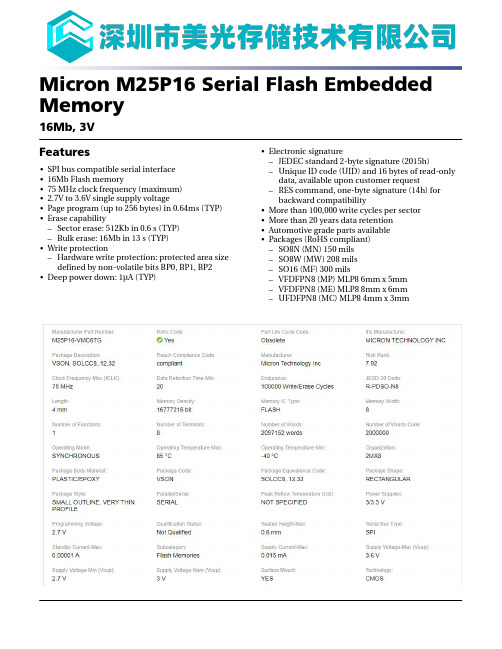
Micron M25P16 Serial Flash Embedded Memory16Mb, 3V Features•SPI bus compatible serial interface •16Mb Flash memory•75 MHz clock frequency (maximum)•2.7V to 3.6V single supply voltage•Page program (up to 256 bytes) in 0.64ms (TYP)•Erase capability–Sector erase: 512Kb in 0.6 s (TYP)–Bulk erase: 16Mb in 13 s (TYP)•Write protection–Hardware write protection: protected area size defined by non-volatile bits BP0, BP1, BP2•Deep power down: 1µA (TYP)•Electronic signature–JEDEC standard 2-byte signature (2015h)–Unique ID code (UID) and 16 bytes of read-only data, available upon customer request–RES command, one-byte signature (14h) for backward compatibility•More than 100,000 write cycles per sector •More than 20 years data retention •Automotive grade parts available •Packages (RoHS compliant)–SO8N (MN) 150 mils –SO8W (MW) 208 mils –SO16 (MF) 300 mils–VFDFPN8 (MP) MLP8 6mm x 5mm –VFDFPN8 (ME) MLP8 8mm x 6mm –UFDFPN8 (MC) MLP8 4mm x 3mmMicron M25P16 Serial Flash Embedded MemoryImportant Notes and WarningsFunctional DescriptionThe M25P16 is an 16Mb (2Mb x 8) serial Flash memory device with advanced write pro-tection mechanisms accessed by a high speed SPI-compatible bus. The device supports high-performance commands for clock frequency up to 75MHz.The memory can be programmed 1 to 256 bytes at a time using the PAGE PROGRAM command. It is organized as 32 sectors, each containing 256 pages. Each page is 256bytes wide. Memory can be viewed either as 8,192 pages or as 2,097,152 bytes. The en-tire memory can be erased using the BULK ERASE command, or it can be erased one sector at a time using the SECTOR ERASE command.This datasheet details the functionality of the M25P16 device based on 110nm process.Figure 1: Logic DiagramS#V CCHOLD#V SSDQ1C DQ0W#Table 1: Signal NamesMicron M25P16 Serial Flash Embedded MemoryFunctional DescriptionFigure 5: Bus Master and Memory Devices on the SPI BusSS2.Resistors (R) ensure that the memory device is not selected if the bus master leaves theS# line High-Z.3.The bus master may enter a state where all I/O are High-Z at the same time; for exam-ple, when the bus master is reset. Therefore, C must be connected to an external pull-down resistor so that when all I/O are High-Z, S# is pulled HIGH while C is pulled LOW.This ensures that S# and C do not go HIGH at the same time and that the t SHCH require-ment is met.4.The typical value of R is 100kΩ, assuming that the time constant R × C p (C p = parasiticcapacitance of the bus line) is shorter than the time during which the bus master leavesthe SPI bus High-Z.5.Example: Given that C p = 50pF (R × C p= 5μs), the application must ensure that the busmaster never leaves the SPI bus High-Z for a time period shorter than 5μs.质量等级领域:宇航级IC、特军级IC、超军级IC、普军级IC、禁运IC、工业级IC,军级二三极管,功率管等;应用领域:航空航天、船舶、汽车电子、军用计算机、铁路、医疗电子、通信网络、电力工业以及大型工业设备祝您:工作顺利,生活愉快!以深圳市美光存储技术有限公司提供的参数为例,以下为M25P16-VMC6TG的详细参数,仅供参考。
Samsung-NAND-FLASH命名规则

三星的pure nand flash〔就是不带其他模块只是nand flash存储芯片〕的命名规那么如下:1. Memory (K)2. NAND Flash : 93. Small Classification(SLC : Single Level Cell, MLC : Multi Level Cell,SM : Smart Media, S/B : Small Block)1 : SLC 1 Chip XD Card2 : SLC 2 Chip XD Card4 : SLC 4 Chip XD CardA : SLC + Muxed I/ F ChipB : Muxed I/ F ChipD : SLC Dual SME : SLC DUAL (S/ B)F : SLC NormalG : MLC NormalH : MLC QDPJ : Non-Muxed OneNandK : SLC Die StackL : MLC DDPM : MLC DSPN : SLC DSPQ : 4CHIP SMR : SLC 4DIE STACK (S/ B)S : SLC Single SMT : SLC SINGLE (S/ B)U : 2 STACK MSPV : 4 STACK MSPW : SLC 4 Die Stack4~5. Density〔注:实际单位应该是bit,而不是Byte〕12 : 512M16 : 16M28 : 128M32 : 32M40 : 4M56 : 256M64 : 64M80 : 8M1G : 1G2G : 2G4G : 4G8G : 8GAG : 16GBG : 32GCG : 64GDG : 128G00 : NONE6~7. Organization00: NONE08: x816: x168. VccA : 1.65V~3.6VB : 2.7V (2.5V~2.9V)C : 5.0V (4.5V~5.5V)D : 2.65V (2.4V ~ 2.9V)E : 2.3V~3.6VR : 1.8V (1.65V~1.95V)Q : 1.8V (1.7V ~ 1.95V)T : 2.4V~3.0VU : 2.7V~3.6VV : 3.3V (3.0V~3.6V)W : 2.7V~5.5V, 3.0V~5.5V0 : NONE9. Mode0 : Normal1 : Dual nCE & Dual R/ nB4 : Quad nCE & Single R/ nB5 : Quad nCE & Quad R/ nB9 : 1st block OTPA : Mask Option 1L : Low grade10. GenerationM : 1st GenerationA : 2nd GenerationB : 3rd GenerationC : 4th GenerationD : 5th Generation11. "─"12. PackageA : COBB : TBGAC : CHIP BIZD : 63-TBGAE : TSOP1 (Lead-Free, 1217)F : WSOP (Lead-Free)G : FBGAH : TBGA (Lead-Free)I : ULGA (Lead-Free)J : FBGA (Lead-Free)K : TSOP1 (1217)L : LGAM : TLGAN : TLGA2P : TSOP1 (Lead-Free)Q : TSOP2 (Lead-Free)S : SMART MEDIAT : TSOP2U : COB (MMC)V : WSOPW : WAFERY : TSOP113. TempC : CommercialI : IndustrialS : SmartMediaB : SmartMedia BLUE0 : NONE (Containing Wafer, CHIP, BIZ, Exceptionhandling code)3 : Wafer Level 314. Bad BlockA : Apple Bad BlockB : Include Bad BlockD : Daisychain SampleK : Sandisk BinL : 1~5 Bad BlockN : ini. 0 blk, add. 10 blkS : All Good Block0 : NONE (Containing Wafer, CHIP, BIZ, Exceptionhandling code)15. NAND-Reserved0 : Reserved16. Packing Type- Common to all products, except of Mask ROM- Divided into TAPE & REEL(In Mask ROM, divided into TRAY, AMMO Packing Separately) 【举例说明】K9GAG08U0M 详细信息如下:1. Memory (K)2. NAND Flash : 93. Small Classification(SLC : Single Level Cell, MLC : Multi Level Cell,SM : SmartMedia, S/B : Small Block)G : MLC Normal4~5. DensityAG : 16G (Note: 这里单位是bit而不是byte,因此实际大小是16Gb=2GB)0 : Normal (x8)7. Organization0 : NONE 8 : x88. VccU : 2.7V~3.6V9. Mode0 : Normal10. GenerationM : 1st Generation11. "─"12. PackageP : TSOP1 (Lead-Free)13. TempC : Commercial14. Customer Bad BlockB : Include Bad Block15. Pre-Program Version0 : None整体描述就是:K9GAG08U0M是,三星的MLC Nand Flash,工作电压为2.7V~3.6V,x8〔即I/O是8位〕,大小是2GB〔16Gb〕,TSOP1封装。
MN6626中文资料
For Audio Equipment
MN6626
Signal Processing LSI for CD Players
Overview
The MN6626 is a CD signal processing LSI that, on a single chip, provides both basic CD player signal processing (EFM demodulation, error correction, and CLV servo) and extra functionality for increasing the versatility and the performance of the CD player.
49
18.70±0.40 (2.35±0.20)
2.60max.
2.20±0.20
0.10±0.10
0.15 -0.05
+0.10
0.15 SEATING PLANE
(1.50±0.20)
0 to 10°
SYNC DETECTION
FLAG
RESY 16K SRAM SUBCODE DEMODULATION
60 EFM DATA DEMODULATION
SYNC INTERPOLATION PROTECTION
INTERPOLATION SOFT MUTING DIGITAL ATTENUATION
LDG RDG SRDATA SCK LRCK IPFLAG BYTCK FCLK WDCK TX MEMP
SBCK SSEL CLDCK BLKCK
50 58 38 39
Q-CODE REGISTER
欧泰克 936 无铅焊台 说明书

使用说明书实际目 录一、包装清单 (1)二、注意事项 (1)三、部件名称 (2)四、焊台的装置和使用 (2)五、烙铁头的维护和使用 (4)六、保养 (5)七、校准烙铁的温度 (5)八、烙铁头 (5)九、排除故障指南 (6)十、如何检查发热元件和组装电线破损 (7)十一、电路图 (9)十二、规格 (9)十三、部件清单……………………………………………………………10一、包装清单请检查包装,以证实所列清单项目正确无误焊台主机 (1)焊台手柄 (1)烙铁架(包括湿海绵) (1)六角头扳手(1.5mm) (1)使用说明书 (1)二、注意事项▲ 警告本使用说明书之“警告”和“注意”的定义如下:● 警告:滥用可能导致使用者死亡或重伤。
● 注意:滥用可能导致使用者受伤或对涉及物体造成实质性破坏。
为您本人安全着想,请严格遵守“注意事项”。
▲ 注意当电源接通时,烙铁头温度高于摄氏200至480度(华氏392至896度)。
鉴于滥用可能导致灼伤或火患,请严格遵守以下事项:● 切勿触及烙铁头附近的金属部分。
● 切勿在易燃物体附近使用烙铁头。
● 通知工厂其它他人士,烙铁头极为灼热,可能引发危险事故。
● 休息时或完工后应关掉电源。
● 更换部件或装置烙铁头时,应关掉电源,并待烙铁头冷却至室温。
B. 添水至下图所示水平面。
小块海绵吸收水分后,可使置于其上的大块海绵一直 保持潮湿状态。
※ 也可以单用大块海绵(省去小块海绵和添水)。
C. 然后沾湿大块清洁海绵,置于烙铁架底座。
2. 连接▲注意:进行连接和解开烙铁时,切记要关掉电源,以免损坏印刷电路板。
A. 将电线装置连接烙铁插座。
B. 将烙铁置放于烙铁座。
C. 将插头插入电源插座。
※ 切记要接地。
3. 设定温度A. 将控温旋钮设定在所需温度点。
B. 锁定控温旋钮。
C. 此焊台配有温度调节钮锁。
按顺时针方向拧紧对准定位然后插入为免损坏焊台,及保持作业环境之安全,应遵守下列事项:● 切勿使用烙铁头进行焊接以外的工作。
6300B系列工业计算机产品选择指南说明书

1 x bootable CFast SATA III slot on board with external rear access 1 x onboard connector for direct insertion of M.2 2242 / 2280 SSD key M PCIex4 2 x onboard connector for 2.5 in. SSD/HDD SATA III 1 or 2 x extractable drawers for 2.5 in. units
Dual 4K Quad core Intel Atom x7-E3950 4 GB
1 x RS232 (DB9M)
1 x DVI-D
2 x PCIe x 4 or 1 x PCI + 1 x PCIe x4 (5 Gb/s), max 10W total
24V DC (18…32V DC) isolated, UPS option (future)
1 x DVI-D 1 x PCI or 1 x PCIe x4 (5 Gb/s) 24V DC (18…32V DC) isolated, UPS option (future)
-20…60 °C
CE, cULus Listed, EAC, KC and RCM Wall, VESA Mount, DIN Rail, Bookshelf, Machine N/A
Dual Single core Intel Atom E3815 1 GB N/A N/A
N/A
Fanless ThinManager® 24V DC
Dell PowerEdge M620 Systems 用户手册说明书

Dell PowerEdge M620 Systems(适用于 Dell PowerEdge VRTX 机柜)用户手册管制型号: HHB管制类型: HHB003注、小心和警告注: “注”表示可以帮助您更好地使用计算机的重要信息。
小心: “小心”表示可能会损坏硬件或导致数据丢失,并说明如何避免此类问题。
警告: “警告”表示可能会造成财产损失、人身伤害甚至死亡。
版权所有© 2014 Dell Inc. 保留所有权利。
本产品受美国、国际版权和知识产权法律保护。
Dell™和 Dell 徽标是 Dell Inc. 在美国和 / 或其他管辖区域的商标。
所有此处提及的其他商标和产品名称可能是其各自所属公司的商标。
2014–10Rev. A01目录1 关于系统 (7)简介 (7)前面板部件和指示灯 (8)使用 USB 软盘或 USB DVD/CD 驱动器 (8)硬盘驱动器功能部件 (8)您可能需要的其他信息 (9)2 使用系统设置程序和引导管理器 (11)选择系统引导模式 (12)进入系统设置 (12)响应错误消息 (12)使用系统设置程序导航键 (12)系统设置选项 (12)系统设置程序主屏幕 (13)系统 BIOS 屏幕 (13)System Information(系统信息)屏幕 (14)Memory Settings(内存设置)屏幕 (14)Processor Settings(处理器设置)屏幕 (15)SATA Settings(SATA 设置)屏幕 (16)Boot Settings(引导设置)屏幕 (16)Integrated Devices(集成设备)屏幕 (17)Serial Communications(串行通信)屏幕 (18)系统配置文件设置屏幕 (18)System Security(系统安全)屏幕 (19)Miscellaneous Settings(其它设置) (20)系统和设置密码功能 (21)分配系统密码和/或设置密码 (21)使用系统密码保护系统安全 (22)删除或更改现有系统密码和/或设置密码 (22)在已启用设置密码的情况下进行操作 (22)进入 UEFI 引导管理器 (23)使用引导管理器导航键 (23)Boot Manager(引导管理器)屏幕 (23)UEFI Boot(UEFI 引导)菜单 (24)嵌入式系统管理 (24)iDRAC 设置公用程序 (24)进入 iDRAC 设置公用程序 (25)3 安装服务器模块组件 (26)建议工具 (26)安装和卸下服务器模块 (26)卸下服务器模块 (26)安装服务器模块 (28)打开与合上服务器模块 (28)打开服务器模块 (28)合上服务器模块 (29)服务器模块内部 (30)冷却导流罩 (30)卸下冷却导流罩 (30)安装冷却导流罩 (31)系统内存 (31)一般内存模块安装原则 (33)模式特定原则 (34)内存配置示例 (35)卸下内存模块 (38)安装内存模块 (39)PCIe 夹层卡 (40)卸下 PCIe 夹层卡 (40)安装 PCIe 夹层卡 (41)管理提升卡 (42)更换 SD 卡 (42)内部 USB 盘 (43)SD vFlash 卡 (43)装回 SD vFlash 卡 (43)网络子卡/LOM 提升卡 (44)卸下网络子卡/LOM 提升卡 (44)安装网络子卡/LOM 提升卡 (45)处理器 (45)卸下处理器 (46)安装处理器 (48)硬盘驱动器 (49)硬盘驱动器/SSD 安装原则 (50)卸下硬盘驱动器/SSD (50)安装硬盘驱动器/SSD (50)进行硬盘驱动器维修前的关机程序 (51)配置引导驱动器 (51)从硬盘驱动器/SSD 托盘中卸下硬盘驱动器/SSD (51)将硬盘驱动器/SSD 安装到硬盘驱动器/SSD 托盘中 (52)硬盘驱动器/SSD 背板 (52)卸下硬盘驱动器/SSD 背板 (52)安装硬盘驱动器/SSD 背板 (53)系统板 (54)卸下系统板 (54)安装系统板 (55)NVRAM 备用电池 (56)更换 NVRAM 备用电池 (56)存储控制器卡 (57)卸下存储控制器卡 (57)安装存储控制器卡 (58)4 系统故障排除 (59)安全第一—为您和您的系统着想 (59)系统内存故障排除 (59)硬盘驱动器故障排除 (59)USB 设备故障排除 (60)内部 SD 卡故障排除 (60)处理器故障排除 (61)系统板故障排除 (61)NVRAM 备用电池故障排除 (61)5 使用系统诊断程序 (63)Dell Online Diagnostics (63)Dell 嵌入式系统诊断程序 (63)何时使用 Embedded System Diagnostics(嵌入式系统诊断程序) (63)运行嵌入式系统诊断程序 (63)从外部介质运行嵌入式系统诊断程序 (64)系统诊断程序控件 (64)6 跳线和连接器 (65)系统板跳线设置 (65)系统板连接器 (66)禁用已忘记的密码 (67)7 技术规格 (68)8 系统消息 (71)LCD 状态信息 (71)查看 LCD 信息 (71)删除 LCD 消息 (71)系统错误消息 (71)警告信息 (141)诊断消息 (142)警报消息 (142)9 获得帮助 (143)联系 Dell (143)1关于系统简介本说明文件提供了有关 Dell PowerEdge M620 服务器模块的信息,该模块专为 PowerEdge VRTX 机柜配置,并且可以通过服务器模块上的标记为PCIe的标签来进行识别。
SiT9366数据手册-1-220MHz任意频率SiTime低抖动差分晶振
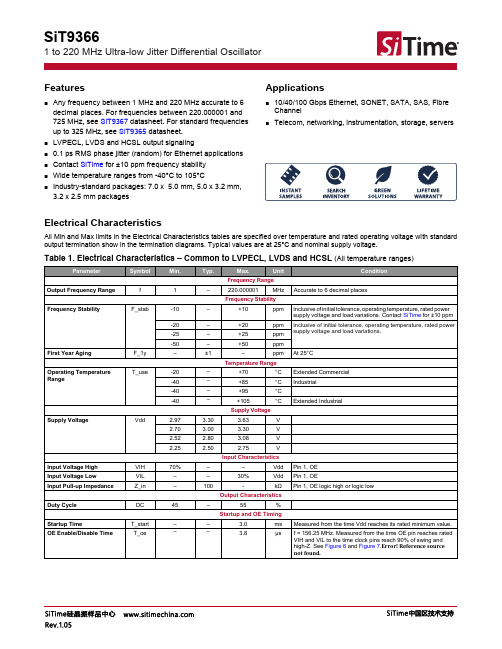
Output Characteristics VOD ΔVOD VOS ΔVOS Tr, Tf 250 – 1.125 – – – – – – 400 450 50 1.375 50 470 mV mV V mV ps See Figure 4 See Figure 4 See Figure 4 See Figure 4 Measured with 2 pF capacitive loading to GND, 20% to 80%, see Figure 5 f = 100, 156.25 or 212.5 MHz, Vdd = 3.3V or 2.5V f = 156.25 MHz, Integration bandwidth = 12 kHz to 20 MHz, all Vdd levels, includes spurs. Temperature ranges -20 to 70ºC and -40 to 85ºC f = 156.25 MHz, Integration bandwidth = 12 kHz to 20 MHz, all Vdd levels, includes spurs. Temperature ranges -40 to 95ºC and -40 to 105ºC f = 156.25 or 322.265625 MHz, IEEE802.3-2005 10GbE jitter mask integration bandwidth = 1.875 MHz to 20 MHz, includes spurs, all Vdd levels. f = 100, 156.25 or 212.5 MHz, Vdd = 3.3V or 2.5V f = 156.25 MHz, Integration bandwidth = 12 kHz to 20 MHz, all Vdd levels, includes spurs. Temperature ranges -20 to 70ºC and -40 to 85ºC f = 156.25 MHz, Integration bandwidth = 12 kHz to 20 MHz, all Vdd levels, includes spurs. Temperature ranges -40 to 95ºC and -40 to 105ºC f = 156.25 or 322.265625 MHz, IEEE802.3-2005 10GbE jitter mask integration bandwidth = 1.875 MHz to 20 MHz, includes spurs, all Vdd levels.
PC87366中文资料

PC87366 128-Pin LPC SuperI/O with System Hardware Monitoring, MIDI and Game PortsGeneral DescriptionThe PC87366,a member of National Semiconductor’s 128-pin LPC SuperI/O family,combines National’s System Hardware Monitoring capability with a Musical Instrument Digital Interface (MIDI)Port and game port inputs for up to two joysticks.The PC87366is PC99and ACPI compliant,and offers a single-chip solution to the most commonly used PC I/O peripherals.System Hardware Monitoring provides minimum power con-sumption and maximum operating efficiency within the system environment.It integrates National’s diode-based or thermistor-based Temperature Sensor (TMS)with National’s Voltage Lev-el Monitor (VLM)for full,PC system thermal control.The PC87366monitors system voltages using 8-bit Analog to Dig-ital (A/D)conversion with seven analog input channels and four internal measuring points.The PC87366also incorporates:Fan Speed Control and Monitor (FSCM)for three fans,extended wake-up support for a wide range of wake-up events,system design protection features,a Floppy Disk Controller (FDC),a Keyboard and Mouse Controller (KBC),a full IEEE 1284Parallel Port,two enhanced Serial Ports (UARTs),one with Infrared (IR)sup-port,ACCESS.bus ®Interface (ACB),System Wake-Up Control (SWC),General-Purpose Input/Output (GPIO)sup-port for 40ports,Interrupt Serializer for Parallel IRQs and an enhanced WATCHDOG ™ timer (WDT).Outstanding FeaturesqSystem Hardware Monitoring including:—Diode-based or thermistor-based T emperature Sen-sor (TMS)—Voltage Level Monitor (VLM) with VID inputs q MIDI interface compatible with MPU-401UART mode q Game port inputs for up to two joysticksqExtended Wake-Up support,including legacy/ACPI power button support,direct power supply control in response to wake-up events,power-fail recovery qProtection features,including chassis intrusion detection,GPIO lock and pin configuration lockq Fan Speed Control and Monitor for three fans q Serial IRQ support (15options)q Interrupt Serializer (11Parallel IRQs to Serial IRQ)qBus interface,based on Intel’s LPC Interface Specifi-cation Revision 1.0,September 29th,1997q ACCESS.bus interface,SMBus physical layer compatible q40GPIO Ports (29standard,including 15with Assert IRQ/SMI/PWUREQs interrupts;11V SB -powered)q Blinking LEDsq128-pin PQFP PackageBlock DiagramSystem Wake-UpSerial Port 2IEEE 1284Parallel PortPorts Keyboard &Mouse I/F SCL ACCESS.bus Floppy Disk ControllerFloppy Drive InterfaceKeyboard &Serial Infrared Interface InterfaceControl Bus InterfaceLPC Interface I/O3 Control WATCHDOGTimer WDOSerial Port 1Serial InterfaceOutputs Fan Speed Control & Monitor Interface Mouse Controllerwith IRGPIO Ports3 Monitor InputsSDA Serial IRQ Analog Inputs System Parallel Port Interface Diode InterfaceSMI PortsHardware MonitoringV REF MIDIInterface MIDI &Game PortsGame Inputs Wake-Up EventsPWUREQ Power Control V DD V BdAT V SBAV DD ACCESS.bus® is a registered trademark of Digital Equipment Corporation.I2C® is a registered trademark of Philips Corporation.IBM®, MicroChannel®, PC-AT® and PS/2® are registered trademarks of International Business Machines Corporation.Microsoft® and Windows® are registered trademarks of Microsoft Corporation.TRI-STATE® is a registered trademark of National Semiconductor Corporation.WATCHDOG‰ is a trademark of National Semiconductor Corporation.SMBus® is a registered trademark of Intel Corporation.© 1999 National Semiconductor CorporationPRELIMINARYJanuary 11,1999PC87366128-Pin LPC SuperI/O with System Hardware Monitoring,MIDI and Game PortsFeatures•Voltage Level Monitor (VLM)—Seven analog inputs that can support both positive and negative voltages—Four internal measuring points—Three thermistor-based temperature monitoring channels—Internal or external V REF—VID inputs—Meets ACPI and DMI requirements for system volt-age monitoring•Temperature Sensor (TMS)—Up to two remote diode inputs—Environment temperature sensing via an internal di-ode—A/D analog channels provide thermal inputs to di-rectly sense die temperature of remote diodes —Meets ACPI and DMI requirements for thermal man-agement—Standby mode to minimize power consumption •Extended Wake-Up—Legacy and ACPI power button support—Direct power supply control in response to wake-up events—Power-fail recovery•Musical Instrument Digital Interface (MIDI) Port —Compatible with MPU-401 UART mode—16-byte Receive and T ransmit FIFOs—Loopback mode supportq Game Port—Full digital implementation—Supports up to two analog joysticks •Protection—Chassis intrusion detection (CHASI, CHASO)—GPIO lock—Pin configuration lock•40 General-Purpose I/O (GPIO) Ports—29standard,with Assert IRQ/SMI/PWUREQ for15 ports—11 V SB-powered—Programmable drive type for each output pin(open-drain, push-pull or output disable)—Programmable option for internal pull-up resistor on each input pin—Output lock option—Input debounce mechanism•Fan Speed Control and Fan Speed Monitor (FSCM)—Supports different fan types—Speed monitoring for three fanst Digital filtering of the tachometer input signalt Alarm for fan slower than programmable thresh-old speedt Alarm for fan stop—Three speed control lines with Pulse Width Modula-tion (PWM)t Output signal in the range of 6 Hz to 93.75 KHzt Duty cycle resolution of 1/256•LPC System Interface—Synchronous cycles, up to 33 MHz bus clock—8-bit I/O cycles—Up to four DMA channels—8-bit DMA cycles—Basic read,write and DMA bus cycles are13clock cycles long•PC99 and ACPI Compliant—PnP Configuration Register structure—Flexible resource allocation for all logical devices t Relocatable base addresst15 IRQ routing optionst4optional8-bit DMA channels(where applicable)•Floppy Disk Controller (FDC)—Programmable write protect—FM and MFM mode support—Enhanced mode command for three-mode Floppy Disk Drive (FDD) support—Perpendicular recording drive support for 2.88 MB—Burst and non-burst modes—Full support for IBM T ape Drive register(TDR)im-plementation of AT and PS/2 drive types—16-byte FIFO—Software compatible with the PC8477,which con-tains a superset of the FDC functions in themicroDP8473,the NEC microPD765A and theN82077—High-performance, digital separator—Standard 5.25” and 3.5” FDD support•Parallel Port—Software or hardware control—Enhanced Parallel Port(EPP)compatible with new version EPP 1.9 and IEEE 1284 compliant—EPP support for version EPP1.7of the Xircom spec-ification—EPP support as mode4of the Extended Capabilities Port (ECP)—IEEE 1284 compliant ECP, including level 2—Selection of internal pull-up or pull-down resistor for Paper End (PE) pin—PCI bus utilization reduction by supporting a de-mand DMA mode mechanism and a DMA fairnessmechanism—Protection circuit that prevents damage to the paral-lel port when a printer connected to it powers up oris operated at high voltages,even if the device is inpower-down—Output buffers that can sink and source 14 mA•Serial Port 1 (UART1)—Software compatible with the 16550A and the 164502Features(Continued)3—Shadow register support for write-only bit monitoring —UART data rates up to 1.5 Mbaud•Serial Port 2 with Infrared (UART2)—Software compatible with the 16550A and the 16450—Shadow register support for write-only bit monitoring —UART data rates up to 1.5 Mbaud —HP-SIR—ASK-IR option of SHARP-IR —DASK-IR option of SHARP-IR—Consumer Remote Control supports RC-5,RC-6,NEC, RCA and RECS 80—Non-standard DMA support −1 or 2 channels —PnP dongle support •Keyboard and Mouse Controller (KBC)—8-bit microcontroller—Software compatible with the 8042AH and PC87911microcontrollers— 2 KB custom-designed program ROM —256 bytes RAM for data—Five programmable dedicated open-drain I/O lines —Asynchronous access to two data registers and onestatus register during normal operation —Support for both interrupt and polling —93 instructions —8-bit timer/counter—Support for binary and BCD arithmetic—Operation at 8MHz,12MHz or 16MHz (programma-ble option)—Can be customized by using the PC87323,which in-cludes a RAM-based KBC as a development plat-form for KBC code•ACCESS.bus Interface (ACB)—Serial interface compatible with SMBus physical layer —Compatible with Philips’ I 2C ®—ACB master and slave—Supports polling and interrupt controlled operation —Optional internal pull-up on SDA and SCL pins•WATCHDOG Timer (WDT)—Times out the system based on user-programmabletime-out period—System power-down capability for power saving —User-defined trigger events to restart WATCHDOG —Optional routing of WATCHDOG output on IRQand/or SMI lines•System Wake-Up Control (SWC)—Power-up request upon detection of Keyboard,Mouse,RI1,RI2,RING activity and General-Pur-pose Input Events, as follows:t Preprogrammed Keyboard or Mouse sequence t External modem ring on serial portt Ring pulse or pulse train on the RING input signal t Preprogrammed CEIR address in a preselectedstandard (NEC, RCA or RC-5)t General-Purpose Input Events t IRQs of internal logical devices —Optional routing of power-up request on IRQ,SMIand/or PWBTOUT—Battery-backed event configuration—Programmable V SB -powered output for blinkingLEDs (LED1, LED2) control•Clock Sources—48 MHz clock input—LPC clock, up to 33 MHz—On-chip low frequency clock generator for wake-up•Power Supplies— 3.3V supply operation —Main (V DD and AV DD )—Standby (V SB )—Battery backup (V BA T )—All pins are 5V tolerant and back-drive protected,ex-cept LPC bus pins•Strap Configuration—Base Address (BADDR)strap to determine the baseaddress of the Index-Data register pair—T est strap to force the device into test mode (re-served for National Semiconductor use)—Power Supply and LED Configuration (PSLDC0,1)straps to determine the power suppy control func-tions and the V SB power-up defaults of LED2—Power Supply On Polarity (PSONPOL)strap to setPSON active state and output typeDatasheet Revision RecordRevision Date Status CommentsNovember1998Draft0.3Specification subject to change without notice;MIDI andGame Port information is incompleteJanuary1999Preliminary1.0Specification subject to change without notice;PowerSupply Control and LED sections in Chapter2areincompleteItem Topic Change/Correction Location 4Table of ContentsDatasheet Revision Record (4) (4)1.0Signal/Pin Connection and Description1.1CONNECTION DIAGRAM (16)1.2BUFFER TYPES AND SIGNAL/PIN DIRECTORY (17)1.3PIN MULTIPLEXING (22)1.4DETAILED SIGNAL/PIN DESCRIPTIONS (24)1.4.1ACCESS.bus Interface (ACB) (24)1.4.2Bus Interface (24)1.4.3Clock (24)1.4.4Fan Speed Control and Monitor (FSCM) (24)1.4.5Floppy Disk Controller (FDC) (25)1.4.6Game Port (26)1.4.7General-Purpose Input/Output (GPIO) Ports (26)1.4.8Infrared (IR) (26)1.4.9Keyboard and Mouse Controller (KBC) (27)1.4.10Musical Instrument Digital Interface (MIDI) Port (27)1.4.11Parallel Port (28)1.4.12Power and Ground (28)1.4.13Protection (29)1.4.14Serial Port 1 and Serial Port 2 (29)1.4.15Strap Configuration (30)1.4.16System Hardware Monitoring (30)1.4.17System Wake-Up Control (31)1.4.18WATCHDOG Timer (WDT) (31)1.5INTERNAL PULL-UP AND PULL-DOWN RESISTORS (32)2.0Device Architecture and Configuration2.1OVERVIEW (34)2.2CONFIGURATION STRUCTURE AND ACCESS (34)2.2.1The Index-Data Register Pair (34)2.2.2Banked Logical Device Registers Structure (36)2.2.3Standard Logical Device Configuration Register Definitions (37)2.2.4Standard Configuration Registers (39)2.2.5Default Configuration Setup (40)2.2.6Power States (40)2.2.7Address Decoding (41)2.3PROTECTION (41)2.3.1Chassis Intrusion Detection (41)2.3.2Pin Configuration Lock (41)2.3.3GPIO Pin Function Lock (42)2.4POWER SUPPLY CONTROL (PSC) (42)2.5LED OPERATION AND STATES (44)2.6POWER SUPPLY CONTROL AND LED CONFIGURATION (44)2.7REGISTER TYPE ABBREVIATIONS (45)2.8SUPERI/O CONFIGURATION REGISTERS (45)2.8.1SuperI/O ID Register (SID) (46)2.8.2SuperI/O Configuration 1 Register (SIOCF1) (46)2.8.3SuperI/O Configuration 2 Register (SIOCF2) (47)2.8.4SuperI/O Configuration 3 Register (SIOCF3) (48)2.8.5SuperI/O Configuration 4 Register (SIOCF4) (49)2.8.6SuperI/O Configuration 5 Register (SIOCF5) (50)2.8.7SuperI/O Revision ID Register (SRID) (50)2.8.8SuperI/O Configuration 8 Register (SIOCF8) (51)2.8.9SuperI/O Configuration A Register (SIOCFA) (52)2.8.10SuperI/O Configuration B Register (SIOCFB) (53)2.8.11SuperI/O Configuration C Register (SIOCFC) (54)2.8.12SuperI/O Configuration D Register (SIOCFD) (55)2.9FLOPPY DISK CONTROLLER (FDC) CONFIGURATION (56)2.9.1General Description (56)2.9.2Logical Device 0 (FDC) Configuration (56)2.9.3FDC Configuration Register (57)2.9.4Drive ID Register (58)2.10PARALLEL PORT CONFIGURATION (59)2.10.1General Description (59)2.10.2Logical Device 1 (PP) Configuration (60)2.10.3Parallel Port Configuration Register (60)2.11SERIAL PORT 2 CONFIGURATION (61)2.11.1General Description (61)2.11.2Logical Device 2 (SP2) Configuration (61)2.11.3Serial Port 2 Configuration Register (61)2.12SERIAL PORT 1 CONFIGURATION (62)2.12.1Logical Device 3 (SP1) Configuration (62)2.12.2Serial Port 1 Configuration Register (62)2.13SYSTEM WAKE-UP CONTROL (SWC) CONFIGURATION (63)2.13.1Logical Device 4 (SWC) Configuration (63)2.14KEYBOARD AND MOUSE CONTROLLER (KBC) CONFIGURATION (64)2.14.1General Description (64)2.14.2Logical Devices 5 and 6 (Mouse and Keyboard) Configuration (65)2.14.3KBC Configuration Register (66)2.15GENERAL-PURPOSE INPUT/OUTPUT (GPIO) PORTS CONFIGURATION (67)2.15.1General Description (67)2.15.2Implementation (67)2.15.3Logical Device 7 (GPIO) Configuration (68)2.15.4GPIO Pin Select Register (69)2.15.5GPIO Pin Configuration Register (70)2.15.6GPIO Event Routing Register (71)62.16ACCESS.BUS INTERFACE (ACB) CONFIGURATION (72)2.16.1General Description (72)2.16.2Logical Device 8 (ACB) Configuration (72)2.16.3ACB Configuration Register (73)2.17FAN SPEED CONTROL AND MONITOR (FSCM) CONFIGURATION (74)2.17.1General Description (74)2.17.2Logical Device 9 (FSCM) Configuration (74)2.17.3Fan Speed Control and Monitor Configuration 1 Register (75)2.17.4Fan Speed Control and Monitor Configuration 2 Register (76)2.17.5Fan Speed Control OTS Configuration Register (76)2.18WATCHDOG TIMER (WDT) CONFIGURATION (77)2.18.1Logical Device 10 (WDT) Configuration (77)2.18.2WATCHDOG Timer Configuration Register (77)2.19GAME PORT (GMP) CONFIGURATION (78)2.19.1Logical Device 11 (GMP) Configuration (78)2.19.2Game Port Configuration Register (78)2.20MIDI PORT (MIDI) CONFIGURATION (79)2.20.1Logical Device 12 (MIDI) Configuration (79)2.20.2MIDI Port Configuration Register (79)2.21VOLTAGE LEVEL MONITOR (VLM) CONFIGURATION (80)2.21.1Logical Device 13 (VLM) Configuration (80)2.22TEMPERATURE SENSOR (TMS) CONFIGURATION (80)2.22.1Logical Device 14 (TMS) Configuration (80)3.0System Wake-Up Control (SWC)3.1OVERVIEW (81)3.2FUNCTIONAL DESCRIPTION (82)3.3EVENT DETECTION (83)3.3.1Modem Ring (83)3.3.2Telephone Ring (83)3.3.3Keyboard and Mouse Activity (84)3.3.4CEIR Address (84)3.3.5Standby General-Purpose Input Events (84)3.3.6GPIO-Triggered Events (84)3.3.7Software Event (84)3.3.8Module IRQ Wake-Up Event (85)3.4SWC REGISTERS (85)3.4.1SWC Register Map (85)3.4.2Wake-Up Events Status Register 0 (WK_STS0) (88)3.4.3Wake-Up Events Status Register (WK_STS1) (89)3.4.4Wake-Up Events Enable Register (WK_EN0) (90)3.4.5Wake-Up Events Enable Register 1 (WK_EN1) (91)3.4.6Wake-Up Configuration Register (WK_CFG) (92)3.4.7Wake-Up Events Routing to SMI Enable Register 0 (WK_SMIEN0) (93)3.4.8Wake-Up Events Routing to SMI Enable Register 1 (WK_SMIEN1) (94)3.4.9Wake-Up Events Routing to IRQ Enable Register 0 (WK_IRQEN0) (95)3.4.10Wake-Up Events Routing to IRQ Enable Register 1 (WK_IRQEN1) (96)3.4.11Wake-Up Extension 1 Enable Register 0 (WK_X1EN0) (97)3.4.12Wake-Up Extension 1 Enable Register 1 (WK_X1EN1) (98)3.4.13Wake-Up Extension 2 Enable Register 0 (WK_X2EN0) (99)3.4.14Wake-Up Extension 2 Enable Register 1 (WK_X2EN1) (100)3.4.15Wake-Up Extension 3 Enable Register 0 (WK_X3EN0) (101)3.4.16Wake-Up Extension 3 Enable Register 1 (WK_X3EN1) (102)3.4.17PS/2 Keyboard and Mouse Wake-Up Events (103)3.4.18PS/2 Protocol Control Register (PS2CTL) (104)3.4.19Keyboard Data Shift Register (KDSR) (104)3.4.20Mouse Data Shift Register (MDSR) (105)3.4.21PS/2 Keyboard Key Data Registers (PS2KEY0 - PS2KEY7) (105)3.4.22CEIR Wake-Up Control Register (IRWCR) (106)3.4.23CEIR Wake-Up Address Register (IRWAD) (107)3.4.24CEIR Wake-Up Address Mask Register (IRWAM) (107)3.4.25CEIR Address Shift Register (ADSR) (108)3.4.26CEIR Wake-Up Range 0 Registers (108)3.4.27CEIR Wake-Up Range 1 Registers (109)3.4.28CEIR Wake-Up Range 2 Registers (109)3.4.29CEIR Wake-Up Range 3 Registers (110)3.4.30Standby General-Purpose I/O (SBGPIO) Register Overview (111)3.4.31Standby GPIO Pin Select Register (SBGPSEL) (114)3.4.32Standby GPIO Pin Configuration Register (SBGPCFG) (115)3.4.33Standby GPIOE/GPIE Data Out Register 0 (SB_GPDO0) (117)3.4.34Standby GPIOE/GPIE Data In Register 0 (SB_GPDI0) (117)3.4.35Standby GPOS Data Out Register 1 (SB_GPDO1) (118)3.4.36Standby GPIS Data In Register 1 (SB_GPDI1) (118)3.5SWC REGISTER BITMAP (119)4.0Fan Speed Control4.1OVERVIEW (123)4.2FUNCTIONAL DESCRIPTION (123)4.3FAN SPEED CONTROL REGISTERS (124)4.3.1Fan Speed Control Register Map (124)4.3.2Fan Speed Control Pre-Scale Register (FCPSR) (124)4.3.3Fan Speed Control Duty Cycle Register (FCDCR) (125)4.4FAN SPEED CONTROL BITMAP (125)5.0Fan Speed Monitor5.1OVERVIEW (126)5.2FUNCTIONAL DESCRIPTION (126)5.3FAN SPEED MONITOR REGISTERS (127)5.3.1Fan Speed Monitor Register Map (127)85.3.2Fan Monitor Threshold Register (FMTHR) (128)5.3.3Fan Monitor Speed Register (FMSPR) (128)5.3.4Fan Monitor Control and Status Register (FMCSR) (128)5.4FAN SPEED MONITOR BITMAP (129)6.0General-Purpose Input/Output (GPIO) Port6.1OVERVIEW (130)6.2BASIC FUNCTIONALITY (131)6.2.1Configuration Options (131)6.2.2Operation (131)6.3EVENT HANDLING AND SYSTEM NOTIFICATION (132)6.3.1Event Configuration (132)6.3.2System Notification (132)6.4GPIO PORT REGISTERS (133)6.4.1GPIO Pin Configuration (GPCFG) Register (134)6.4.2GPIO Pin Event Routing (GPEVR) Register (135)6.4.3GPIO Port Runtime Register Map (135)6.4.4GPIO Data Out Register (GPDO) (136)6.4.5GPIO Data In Register (GPDI) (136)6.4.6GPIO Event Enable Register (GPEVEN) (137)6.4.7GPIO Event Status Register (GPEVST) (137)7.0WATCHDOG Timer (WDT)7.1OVERVIEW (138)7.2FUNCTIONAL DESCRIPTION (138)7.3WATCHDOG TIMER REGISTERS (139)7.3.1WATCHDOG Timer Register Map (139)7.3.2WATCHDOG Timeout Register (WDTO) (139)7.3.3WATCHDOG Mask Register (WDMSK) (140)7.3.4WATCHDOG Status Register (WDST) (141)7.4WATCHDOG TIMER REGISTER BITMAP (141)8.0ACCESS.bus Interface (ACB)8.1OVERVIEW (142)8.2FUNCTIONAL DESCRIPTION (142)8.2.1Data Transactions (142)8.2.2Start and Stop Conditions (142)8.2.3Acknowledge (ACK) Cycle (143)8.2.4Acknowledge after Every Byte Rule (144)8.2.5Addressing Transfer Formats (144)8.2.6Arbitration on the Bus (144)8.2.7Master Mode (145)8.2.8Slave Mode (147)8.2.9Configuration (147)8.3ACB REGISTERS (148)8.3.1ACB Register Map (148)8.3.2ACB Serial Data Register (ACBSDA) (148)8.3.3ACB Status Register (ACBST) (149)8.3.4ACB Control Status Register (ACBCST) (150)8.3.5ACB Control Register 1 (ACBCTL1) (151)8.3.6ACB Own Address Register (ACBADDR) (152)8.3.7ACB Control Register 2 (ACBCTL2) (152)8.4ACB REGISTER BITMAP (153)9.0Game Port (GMP)9.1OVERVIEW (154)9.2FUNCTIONAL DESCRIPTION (154)9.2.1Game Device Axis Position Indication (154)9.2.2Capturing the Position (155)9.2.3Button Status Indication (156)9.2.4Operation Modes (156)9.2.5Operation Control (157)9.3GAME PORT REGISTERS (158)9.3.1Game Port Register Map (158)9.3.2Game Port Control Register (GMPCTL) (159)9.3.3Game Port Legacy Status Register (GMPLST) (160)9.3.4Game Port Extended Status Register (GMPXST) (161)9.3.5Game Port Interrupt Enable Register (GMPIEN) (162)9.3.6Game Device A X-Axis Position Low Byte (GMPAXL) (163)9.3.7Game Device A X-Axis Position High Byte (GMPAXH) (163)9.3.8Game Device A YAxis Position Low Byte (GMPAYL) (163)9.3.9Game Device A Y-Axis Position High Byte (GMPAYH) (163)9.3.10Game Device B X-Axis Position Low Byte (GMPBXL) (164)9.3.11Game Device B X-Axis Position High Byte (GMPBXH) (164)9.3.12Game Device B Y-Axis Position Low Byte (GMPBYL) (164)9.3.13Game Device B Y-Axis Position High Byte (GMPBYH) (164)9.3.14Game Port Event Polarity Register (GMPEPOL) (165)9.4GAME PORT BITMAP (166)10.0Musical Instrument Digital Interface (MIDI) Port10.1OVERVIEW (167)10.2FUNCTIONAL DESCRIPTION (167)10.2.1Internal Bus Interface Unit (168)10.2.2Port Control and Status Registers (168)10.2.3Data Buffers and FIFOs (168)10.2.4MIDI Communication Engine (168)10.2.5MIDI Signals Routing Control Logic (169)10.2.6Operation Modes (169)10.2.7MIDI Port Status Flags (170)1010.2.8MIDI Port Interrupts (171)10.2.9Enhanced MIDI Port Features (172)10.3MIDI PORT REGISTERS (173)10.3.1MIDI Port Register Map (173)10.3.2MIDI Data In Register (MDI) (173)10.3.3MIDI Data Out Register (MDO) (173)10.3.4MIDI Status Register (MSTAT) (174)10.3.5MIDI Command Register (MCOM) (174)10.3.6MIDI Control Register (MCNTL) (175)10.4MIDI PORT BITMAP (176)11.0Voltage Level Monitor (VLM)11.1OVERVIEW (177)11.2FUNCTIONAL DESCRIPTION (177)11.2.1Voltage Measurement, Channels 0 through 10 (178)11.2.2Thermistor-Based Temperature Measurement, Channels 11 to 13 (179)11.2.3 V OS, V HIGH and V LOW Limits, OTS and ALERT Output, IRQ and SMI (179)11.2.4Power-On Reset Default States (180)11.2.5Standby Mode (180)11.3ANALOG SUPPLY CONNECTION (180)11.3.1Recommendations (180)11.3.2Reference Voltage (181)11.4REGISTER BANK OVERVIEW (181)11.5VLM REGISTERS (182)11.5.1VLM Register Map (182)11.5.2Voltage Event Status Register 0 (VEVSTS0) (183)11.5.3Voltage Event Status Register 1 (VEVSTS1) (183)11.5.4Voltage Event to SMI Register 0 (VEVSMI0) (184)11.5.5Voltage Event to SMI Register 1 (VEVSMI1) (185)11.5.6Voltage Event to IRQ Register 0 (VEVIRQ0) (186)11.5.7Voltage Event to IRQ Register 1 (VEVIRQ1) (186)11.5.8Voltage ID Register (VID) (187)11.5.9Voltage Conversion Rate Register (VCNVR) (188)11.5.10VLM Configuration Register (VLMCFG) (189)11.5.11VLM Bank Select Register (VLMBS) (189)11.5.12Voltage Channel Configuration and Status Register (VCHCFST) (190)11.5.13Read Channel Voltage Register (RDCHV) (191)11.5.14Channel Voltage High Limit Register (CHVH) (191)11.5.15Channel Voltage Low Limit Register (CHVL) (191)11.5.16Overtemperature Shutdown Limit Register (OTSL) (191)11.6VLM REGISTER BITMAP (192)11.6.1VLM Control and Status Registers (192)11.6.2VLM Channel Registers (192)11.7USAGE HINTS (193)11.7.2Measuring Out of Range Positive and Negative Voltages (194)12.0Temperature Sensor (TMS)12.1OVERVIEW (195)12.2FUNCTIONAL DESCRIPTION (195)12.2.1Register Bank Overview (196)12.2.2T OS, T HIGH and T LOW Limits, OTS and ALERT Output, IRQ and SMI (196)12.2.3ALERT Response Read Sequence (197)12.2.4Power-On Reset Default States (197)12.2.5Temperature Data Format (198)12.2.6Standby Mode (198)12.2.7Diode Fault Detection (198)12.3TMS REGISTERS (199)12.3.1TMS Register Map (199)12.3.2Temperature Event Status Register (TEVSTS) (200)12.3.3Temperature Event to SMI Register (TEVSMI) (201)12.3.4Temperature Event to IRQ Register (TEVIRQ) (202)12.3.5TMS Configuration Register (TMSCFG) (203)12.3.6TMS Bank Select Register (TMSBS) (203)12.3.7Temperature Channel Configuration and Status Register (TCHCFST) (204)12.3.8Read Channel Temperature Register (RDCHT) (205)12.3.9Channel Temperature High Limit Register (CHTH) (205)12.3.10Channel Temperature Low Limit Register (CHTL) (205)12.3.11Channel Overtemperature Limit Register (CHOTL) (205)12.4TMS REGISTER BITMAP (206)12.4.1TMS Control and Status Registers (206)12.4.2TMS Channel Registers (206)12.5USAGE HINTS (206)12.5.1Remote Diode Selection (206)12.5.2ADC Noise Filtering (207)12.5.3PC Board Layout (207)12.5.4Twisted Pair and Shielded Cables (209)13.0Legacy Functional Blocks13.1KEYBOARD AND MOUSE CONTROLLER (KBC) (210)13.1.1General Description (210)13.1.2KBC Register Map (210)13.1.3KBC Bitmap Summary (210)13.2FLOPPY DISK CONTROLLER (FDC) (211)13.2.1General Description (211)13.2.2FDC Register Map (211)13.2.3FDC Bitmap Summary (212)13.3PARALLEL PORT (213)13.3.1General Description (213)13.3.3Parallel Port Bitmap Summary (214)13.4UART FUNCTIONALITY (SP1 AND SP2) (216)13.4.1General Description (216)13.4.2UART Mode Register Bank Overview (216)13.4.3SP1 and SP2 Register Maps for UART Functionality (217)13.4.4SP1 and SP2 Bitmap Summary for UART Functionality (219)13.5IR FUNCTIONALITY (SP2) (221)13.5.1General Description (221)13.5.2IR Mode Register Bank Overview (221)13.5.3SP2 Register Map for IR Functionality (222)13.5.4SP2 Bitmap Summary for IR Functionality (223)14.0Device Characteristics14.1GENERAL DC ELECTRICAL CHARACTERISTICS (225)14.1.1Recommended Operating Conditions (225)14.1.2Absolute Maximum Ratings (225)14.1.3Capacitance (225)14.1.4Power Consumption under Recommended Operating Conditions (226)14.2DC CHARACTERISTICS OF PINS, BY I/O BUFFER TYPES (226)14.2.1Input, CMOS Compatible (226)14.2.2Input, PCI 3.3V (226)14.2.3Input, SMBus Compatible (227)14.2.4Input, Strap Pin (227)14.2.5Input, TTL Compatible (227)14.2.6Input, TTL Compatible with Schmitt Trigger (227)14.2.7Output, PCI 3.3V (228)14.2.8Output, Totem-Pole Buffer (228)14.2.9Output, Open-Drain Buffer (228)14.2.10Input, Analog (228)14.2.11Input, Analog (228)14.2.12Input, Analog (229)14.2.13Output, Analog (229)14.2.14Output, Analog (229)14.2.15Exceptions (229)14.3INTERNAL RESISTORS (230)14.3.1Pull-Up Resistor (230)14.3.2Pull-Down Resistor (230)14.4ANALOG CHARACTERISTICS (230)14.4.1VLM (230)14.4.2TMS (230)14.5AC ELECTRICAL CHARACTERISTICS (232)14.5.1AC Test Conditions (232)14.5.2Clock Timing (232)14.5.3LCLK and LRESET (233)14.5.5Serial Port, Sharp-IR, SIR and Consumer Remote Control Timing (235)14.5.6Modem Control Timing (236)14.5.7FDC Write Data Timing (236)14.5.8FDC Drive Control Timing (237)14.5.9FDC Read Data Timing (237)14.5.10Standard Parallel Port Timing (238)14.5.11Enhanced Parallel Port Timing (238)14.5.12Extended Capabilities Port (ECP) Timing (239)。
iw3616、3617、3630datasheet中文翻译(绝对真实)

产品特色大幅简化离线式LED驱动器设计●单级功率因数校正(PFC)与精确恒流(CC)输出相结合●输入/输出电容和变压器体积小●一次侧反馈控制,无需光耦电路,简化了电路设计●简化初级侧PWM调光接口●符合IEC61000-3-2标准高效节能和高兼容性●大幅提升效率,可达到85%以上●减少元件数量●总谐波失真<15%且PF>0.95●前沿、后沿和数字调光器●传感器和定时器精确稳定的性能●LED负载恒流精度不低于±5%●支持LED负载热插拔●1%-100%宽范围调光,调光无闪烁先进的保护及安全特性●通过自动重启动提供短路保护●开路故障检测模式●自动热关断重启动无论在PCB板上还是在封装上,都保证高压漏极引脚与其他所有信号引脚之间满足高压爬电要求应用●LED离线固态照明说明G7617 是一款的适用于LED调光控制的离线式两级交流/直流电源控制器,是适用于25W 输出功率的可调光LED 灯具的最优之选。
G7617符合电磁兼容性(EMC) IEC61000-3-2 标准,在120V AC或230V AC输入电压下其功率因数(PF) 可达到0.95 以上。
采用先进的数控技术来检测调光器的类型和相位,为调光器提供动态阻抗的同时可调节LED发光亮度,自动检测调光器类型和相位,从而实现了业内与模拟及数字调光器最广泛的兼容性。
G7617工作于准谐振工作模式,工作效率高,可工作于前沿后沿调光模式,也可工作于R 型、R-C型或R-L型调光控制模式。
G7617 符合热插拔LED 模块的固态照明行业标准Zhaga,同时还集成了调光功能的映射选项(位于白炽灯替代灯的NEMA SSL6 调光曲线内)。
G7617 系列有两个版本:针对120V AC输入应用进行优化的G7617-00 和针对230V AC 应用进行优化的G7617-01。
订购信息应用框图图1典型应用内部框图Vcc VinVcbVT CFGASU BisenseBdrvFdrvFisensePGNDAGND C O R E图2 内部框图引脚功能描述BV SENSE V IN BI SENSE B DRV CFG ASU V CCV CBV TFV SENSEFI SENSEF DRVAGNDPGND 图3. 引脚布局BV SENSE引脚:PFC电感电压反馈点,用于感知Boost电感的磁通状态。
ITR9606中文资料

160
140
2
120
100 80
60
40
20
0 0 10 20 30 40 50 60 70
Fig.5 Collector Dark Current vs.
Ambient Temperature
10
10 10
10
10
0
25
50 75 100
Fig.4 Collector Current vs. Irradiance
1.3
1.2 IF=20mA
1.1
Ie-Radiant Intensity (mW/sr)
0 25 50 75 100 120
1 25 50 75 100 120
Everlight Electronics Co., Ltd. Device No:CDRX-096-004
http:\\ Prepared date:08-08-2005
http:\\ Prepared date:08-08-2005
Rev 3
Page: 3 of 6
Prepared by:Denky
元器件交易网
█ Typical Electrical/Optical/Characteristics Curves for IR
--- --- 10 μA
VR=5V
--- 940 --- nm
IF=20mA
--- 60 --- Deg
IF=20mA
--- --- 100 nA VCE=20V,Ee=0mW/cm2
VCE(sat) --- --- 0.4 V
IC=2mA ,Ee=1mW/cm2
Collect Current Transfer
M24C04-W1BN6T中文资料
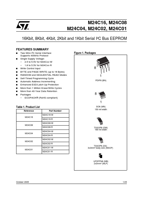
1/25October 2005M24C16, M24C08M24C04, M24C02, M24C0116Kbit, 8Kbit, 4Kbit, 2Kbit and 1Kbit Serial I²C Bus EEPROMFEATURES SUMMARY■Two-Wire I²C Serial Interface Supports 400kHz Protocol ■Single Supply Voltage:– 2.5 to 5.5V for M24Cxx-W – 1.8 to 5.5V for M24Cxx-R ■Write Control Input■BYTE and PAGE WRITE (up to 16 Bytes)■RANDOM and SEQUENTIAL READ Modes ■Self-Timed Programming Cycle ■Automatic Address Incrementing ■Enhanced ESD/Latch-Up Protection ■More than 1 Million Erase/Write Cycles ■More than 40-Year Data Retention ■Packages–ECOPACK® (RoHS compliant)Table 1. Product ListReference Part NumberM24C16M24C16-W M24C16-R M24C08M24C08-W M24C08-R M24C04M24C04-W M24C04-R M24C02M24C02-W M24C02-R M24C01M24C01-W M24C01-RM24C16, M24C08, M24C04, M24C02, M24C01TABLE OF CONTENTSFEATURES SUMMARY . . . . . . . . . . . . . . . . . . . . . . . . . . . . . . . . . . . . . . . . . . . . . . . . . . . . . . . . . . . . .1SUMMARY DESCRIPTION. . . . . . . . . . . . . . . . . . . . . . . . . . . . . . . . . . . . . . . . . . . . . . . . . . . . . . . . . . .3 Device internal reset. . . . . . . . . . . . . . . . . . . . . . . . . . . . . . . . . . . . . . . . . . . . . . . . . . . . . . . . . . . .3SIGNAL DESCRIPTION . . . . . . . . . . . . . . . . . . . . . . . . . . . . . . . . . . . . . . . . . . . . . . . . . . . . . . . . . . . . .4Serial Clock (SCL). . . . . . . . . . . . . . . . . . . . . . . . . . . . . . . . . . . . . . . . . . . . . . . . . . . . . . . . . . . . . . .4 Serial Data (SDA) . . . . . . . . . . . . . . . . . . . . . . . . . . . . . . . . . . . . . . . . . . . . . . . . . . . . . . . . . . . . . . .4 Chip Enable (E0, E1, E2) . . . . . . . . . . . . . . . . . . . . . . . . . . . . . . . . . . . . . . . . . . . . . . . . . . . . . . . . .4 Write Control (WC) . . . . . . . . . . . . . . . . . . . . . . . . . . . . . . . . . . . . . . . . . . . . . . . . . . . . . . . . . . . . . .4DEVICE OPERATION. . . . . . . . . . . . . . . . . . . . . . . . . . . . . . . . . . . . . . . . . . . . . . . . . . . . . . . . . . . . . . .6Start Condition. . . . . . . . . . . . . . . . . . . . . . . . . . . . . . . . . . . . . . . . . . . . . . . . . . . . . . . . . . . . . . . . .6 Stop Condition. . . . . . . . . . . . . . . . . . . . . . . . . . . . . . . . . . . . . . . . . . . . . . . . . . . . . . . . . . . . . . . . .6 Acknowledge Bit (ACK) . . . . . . . . . . . . . . . . . . . . . . . . . . . . . . . . . . . . . . . . . . . . . . . . . . . . . . . . .6 Data Input. . . . . . . . . . . . . . . . . . . . . . . . . . . . . . . . . . . . . . . . . . . . . . . . . . . . . . . . . . . . . . . . . . . . .6 Memory Addressing . . . . . . . . . . . . . . . . . . . . . . . . . . . . . . . . . . . . . . . . . . . . . . . . . . . . . . . . . . . .6 Write Operations . . . . . . . . . . . . . . . . . . . . . . . . . . . . . . . . . . . . . . . . . . . . . . . . . . . . . . . . . . . . . . .7 Byte Write. . . . . . . . . . . . . . . . . . . . . . . . . . . . . . . . . . . . . . . . . . . . . . . . . . . . . . . . . . . . . . . . . . . . .7 Page Write . . . . . . . . . . . . . . . . . . . . . . . . . . . . . . . . . . . . . . . . . . . . . . . . . . . . . . . . . . . . . . . . . . . .7 Minimizing System Delays by Polling On ACK. . . . . . . . . . . . . . . . . . . . . . . . . . . . . . . . . . . . . . .9 Read Operations . . . . . . . . . . . . . . . . . . . . . . . . . . . . . . . . . . . . . . . . . . . . . . . . . . . . . . . . . . . . . .10 Random Address Read. . . . . . . . . . . . . . . . . . . . . . . . . . . . . . . . . . . . . . . . . . . . . . . . . . . . . . . . .10 Current Address Read . . . . . . . . . . . . . . . . . . . . . . . . . . . . . . . . . . . . . . . . . . . . . . . . . . . . . . . . .10 Sequential Read. . . . . . . . . . . . . . . . . . . . . . . . . . . . . . . . . . . . . . . . . . . . . . . . . . . . . . . . . . . . . . .11 Acknowledge in Read Mode. . . . . . . . . . . . . . . . . . . . . . . . . . . . . . . . . . . . . . . . . . . . . . . . . . . . .11INITIAL DELIVERY STATE. . . . . . . . . . . . . . . . . . . . . . . . . . . . . . . . . . . . . . . . . . . . . . . . . . . . . . . . . .11 MAXIMUM RATING. . . . . . . . . . . . . . . . . . . . . . . . . . . . . . . . . . . . . . . . . . . . . . . . . . . . . . . . . . . . . . . .12 DC and AC PARAMETERS . . . . . . . . . . . . . . . . . . . . . . . . . . . . . . . . . . . . . . . . . . . . . . . . . . . . . . . . .13 PACKAGE MECHANICAL . . . . . . . . . . . . . . . . . . . . . . . . . . . . . . . . . . . . . . . . . . . . . . . . . . . . . . . . . .18 PART NUMBERING . . . . . . . . . . . . . . . . . . . . . . . . . . . . . . . . . . . . . . . . . . . . . . . . . . . . . . . . . . . . . . .23 REVISION HISTORY. . . . . . . . . . . . . . . . . . . . . . . . . . . . . . . . . . . . . . . . . . . . . . . . . . . . . . . . . . . . . . .242/253/25M24C16, M24C08, M24C04, M24C02, M24C01SUMMARY DESCRIPTIONThese I²C-compatible electrically erasable pro-grammable memory (EEPROM) devices are orga-nized as 2048/1024/512/256/128x 8 (M24C16,M24C08, M24C04, M24C02 and M24C01).In order to meet environmental requirements, ST offers these devices in ECOPACK® packages.ECOPACK® packages are Lead-free and RoHS compliant.ECOPACK is an ST trademark. ECOPACK speci-fications are available at: .I²C uses a two-wire serial interface, comprising a bi-directional data line and a clock line. The devic-es carry a built-in 4-bit Device Type Identifier code (1010) in accordance with the I²C bus definition.The device behaves as a slave in the I²C protocol,with all memory operations synchronized by the serial clock. Read and Write operations are initiat-ed by a Start condition, generated by the bus mas-ter. The Start condition is followed by a Device scribed in Table 3.), terminated by an acknowl-edge bit.When writing data to the memory, the device in-serts an acknowledge bit during the 9th bit time,following the bus master’s 8-bit transmission.When data is read by the bus master, the bus master acknowledges the receipt of the data byte in the same way. Data transfers are terminated by a Stop condition after an Ack for Write, and after a NoAck for Read.Table 2. Signal NamesDevice internal resetIn order to prevent inadvertent Write operations during Power-up, a Power On Reset (POR) circuit is included. At Power-up (continuous rise of V CC ),the device will not respond to any instructions until the V CC has reached the Power On Reset threshold voltage (this threshold is lower than the V CC min. operating voltage defined in DC and AC PARAMETERS ). When V CC has passed over the POR threshold, the device is reset and is in Standby Power mode. At Power-down (continuous decay of V CC ), as soon as V CC drops from the normal operating voltage to below the Power On Reset threshold voltage, the device stops responding to any instruction sent to it.Prior to selecting and issuing instructions to the memory, a valid and stable V CC voltage must be applied. This voltage must remain stable and valid until the end of the transmission of the instruction and, for a Write instruction, until the completion of the internal write cycle (t W ).Note: 1.NC = Not Connected2.See PACKAGE MECHANICAL section for package dimensions, and how to identify pin-1.E0, E1, E2Chip Enable SDA Serial Data SCL Serial Clock WCWrite Control V CC Supply Voltage V SSGroundM24C16, M24C08, M24C04, M24C02, M24C014/25SIGNAL DESCRIPTIONSerial Clock (SCL).This input signal is used to strobe all data in and out of the device. In applica-tions where this signal is used by slave devices to synchronize the bus to a slower clock, the bus master must have an open drain output, and a pull-up resistor can be connected from Serial Clock (SCL) to V CC . (Figure 5. indicates how the value of the pull-up resistor can be calculated). In most applications, though, this method of synchro-nization is not employed, and so the pull-up resis-tor is not necessary, provided that the bus master has a push-pull (rather than open drain) output.Serial Data (SDA).This bi-directional signal is used to transfer data in or out of the device. It is an open drain output that may be wire-OR’ed with other open drain or open collector signals on the bus. A pull up resistor must be connected from Se-rial Data (SDA) to V CC . (Figure 5. indicates how the value of the pull-up resistor can be calculated).Chip Enable (E0, E1, E2).These input signals are used to set the value that is to be looked for on the three least significant bits (b3, b2, b1) of the 7-bit Device Select Code. These inputs must be tied to V CC or V SS , to establish the Device Select Code as shown in Figure 4.for protecting the entire contents of the memory from inadvertent write operations. Write opera-tions are disabled to the entire memory array when nected, the signal is internally read as V IL , and Write operations are allowed.Select and Address bytes are acknowledged,Data bytes are not acknowledged.M24C16, M24C08, M24C04, M24C02, M24C01Table 3. Device Select CodeDevice Type Identifier1Chip Enable2,3RWb7b6b5b4b3b2b1b0M24C01 Select Code1010E2E1E0RWM24C02 Select Code1010E2E1E0RWM24C04 Select Code1010E2E1A8RWM24C08 Select Code1010E2A9A8RWM24C16 Select Code1010A10A9A8RW Note: 1.The most significant bit, b7, is sent first.2.E0, E1 and E2 are compared against the respective external pins on the memory device.3.A10, A9 and A8 represent most significant bits of the address.5/25M24C16, M24C08, M24C04, M24C02, M24C016/25DEVICE OPERATIONThe device supports the I²C protocol. This is sum-marized in Figure 6.. Any device that sends data on to the bus is defined to be a transmitter, and any device that reads the data to be a receiver.The device that controls the data transfer is known as the bus master, and the other as the slave de-vice. A data transfer can only be initiated by the bus master, which will also provide the serial clock for synchronization. The M24Cxx device is always a slave in all communication.Start ConditionStart is identified by a falling edge of Serial Data (SDA) while Serial Clock (SCL) is stable in the High state. A Start condition must precede any data transfer command. The device continuously monitors (except during a Write cycle) Serial Data (SDA) and Serial Clock (SCL) for a Start condition,and will not respond unless one is given.Stop ConditionStop is identified by a rising edge of Serial Data (SDA) while Serial Clock (SCL) is stable and driv-en High. A Stop condition terminates communica-tion between the device and the bus master. A Read command that is followed by NoAck can be followed by a Stop condition to force the device into the Stand-by mode. A Stop condition at the end of a Write command triggers the internal Write cycle.Acknowledge Bit (ACK)The acknowledge bit is used to indicate a success-ful byte transfer. The bus transmitter, whether it be bus master or slave device, releases Serial Data (SDA) after sending eight bits of data. During the 9th clock pulse period, the receiver pulls Serial Data (SDA) Low to acknowledge the receipt of the eight data bits.Data InputDuring data input, the device samples Serial Data (SDA) on the rising edge of Serial Clock (SCL).For correct device operation, Serial Data (SDA)must be stable during the rising edge of Serial Clock (SCL), and the Serial Data (SDA) signal must change only when Serial Clock (SCL) is driv-en Low.Memory AddressingTo start communication between the bus master and the slave device, the bus master must initiate a Start condition. Following this, the bus master sends the Device Select Code, shown in Table 3.(on Serial Data (SDA), most significant bit first).The Device Select Code consists of a 4-bit Device Type Identifier, and a 3-bit Chip Enable “Address”(E2, E1, E0). To address the memory array, the 4-bit Device Type Identifier is 1010b.Each device is given a unique 3-bit code on the Chip Enable (E0, E1, E2) inputs. When the Device Select Code is received, the device only responds if the Chip Enable Address is the same as the val-ue on the Chip Enable (E0, E1, E2) inputs. How-ever, those devices with larger memory capacities (the M24C16, M24C08 and M24C04) need more address bits. E0 is not available for use on devices that need to use address line A8; E1 is not avail-able for devices that need to use address line A9,and E2 is not available for devices that need to use address line A10 (see Figure 3. and Table 3. for details). Using the E0, E1 and E2 inputs, up to eight M24C02 (or M24C01), four M24C04, two M24C08 or one M24C16 devices can be connect-ed to one I²C bus. In each case, and in the hybrid cases, this gives a total memory capacity of 16Kbits, 2KBytes (except where M24C01 devic-es are used).The 8th set to 1 for Read and 0 for Write operations.If a match occurs on the Device Select code, the corresponding device gives an acknowledgment on Serial Data (SDA) during the 9th bit time. If the device does not match the Device Select code, it deselects itself from the bus, and goes into Stand-by mode.Table 4. Operating ModesNote: 1.X = V IH or V IL .ModeRW bit WC 1Bytes Initial SequenceCurrent Address Read 1X 1START , Device Select, RW = 1Random Address Read 0X 1START , Device Select, RW = 0, Address 1X reST ART, Device Select, RW = 1Sequential Read 1X ≥ 1Similar to Current or Random Address Read Byte Write 0V IL 1START , Device Select, RW = 0Page WriteV IL≤ 16START , Device Select, RW = 0M24C16, M24C08, M24C04, M24C02, M24C01Figure 7. Write Mode Sequences with WC=1 (data write inhibited)Following a Start condition the bus master sends a Device Select Code with the Read/Write bit (RW) reset to 0. The device acknowledges this, as shown in Figure 8., and waits for an address byte. The device responds to the address byte with an acknowledge bit, and then waits for the data byte. When the bus master generates a Stop condition immediately after the Ack bit (in the “10th bit” time slot), either at the end of a Byte Write or a Page Write, the internal Write cycle is triggered. A Stop condition at any other time slot does not trigger the internal Write cycle.During the internal Write cycle, Serial Data (SDA) and Serial Clock (SCL) are ignored, and the de-vice does not respond to any requests.Byte WriteAfter the Device Select code and the address byte, the bus master sends one data byte. If the ad-dressed location is Write-protected, by Write Con-trol (WC) being driven High (during the period from byte), the device replies to the data byte with NoAck, as shown in Figure 7., and the location is not modified. If, instead, the addressed location is not Write-protected, the device replies with Ack. The bus master terminates the transfer by gener-ating a Stop condition, as shown in Figure 8.. Page WriteThe Page Write mode allows up to 16 bytes to be written in a single Write cycle, provided that they are all located in the same page in the memory: that is, the most significant memory address bits are the same. If more bytes are sent than will fit up to the end of the page, a condition known as ‘roll-over’ occurs. This should be avoided, as data starts to become overwritten in an implementation dependent way.The bus master sends from 1 to 16 bytes of data, each of which is acknowledged by the device if Write Control (WC) is Low. If the addressed loca-ing driven High (during the period from the Start7/25M24C16, M24C08, M24C04, M24C02, M24C018/25condition until the end of the address byte), the de-vice replies to the data bytes with NoAck, as shown in Figure 7., and the locations are not mod-ified. After each byte is transferred, the internalbyte address counter (the 4 least significant ad-dress bits only) is incremented. The transfer is ter-minated by the bus master generating a Stop condition.M24C16, M24C08, M24C04, M24C02, M24C01During the internal Write cycle, the device discon-nects itself from the bus, and writes a copy of the data from its internal latches to the memory cells. The maximum Write time (t w) is shown in Table 13. and Table 14., but the typical time is shorter. To make use of this, a polling sequence can be used by the bus master.The sequence, as shown in Figure 9., is:–Step 1: the bus master issues a Start condition followed by a Device Select Code (the firstbyte of the new instruction).–Step 2: if the device is busy with the internal Write cycle, no Ack will be returned and thebus master goes back to Step 1. If the device has terminated the internal Write cycle, itresponds with an Ack, indicating that thedevice is ready to receive the second part of the instruction (the first byte of this instruction having been sent during Step 1).9/25M24C16, M24C08, M24C04, M24C02, M24C0110/25Read OperationsRead operations are performed independently of The device has an internal address counter which is incremented each time a byte is read.Random Address ReadA dummy Write is first performed to load the ad-dress into this address counter (as shown in Fig-ure 10.) but without sending a Stop condition.Then, the bus master sends another Start condi-tion, and repeats the Device Select Code, with the Read/Write bit (RW) set to 1. The device acknowl-edges this, and outputs the contents of the ad-dressed byte. The bus master must not acknowledge the byte, and terminates the transfer with a Stop condition.Current Address ReadFor the Current Address Read operation, following a Start condition, the bus master only sends a De-to 1. The device acknowledges this, and outputs the byte addressed by the internal address counter. The counter is then incremented. The bus master terminates the transfer with a Stop condi-tion, as shown in Figure 10., without acknowledg-ing the byte.Sequential ReadThis operation can be used after a Current Ad-dress Read or a Random Address Read. The bus master does acknowledge the data byte output, and sends additional clock pulses so that the de-vice continues to output the next byte in sequence. To terminate the stream of bytes, the bus master must not acknowledge the last byte, and must generate a Stop condition, as shown in Figure 10.. The output data comes from consecutive address-es, with the internal address counter automatically incremented after each byte output. After the last memory address, the address counter ‘rolls-over’, and the device continues to output data from memory address 00h.Acknowledge in Read ModeFor all Read commands, the device waits, aftereach byte read, for an acknowledgment during the 9th bit time. If the bus master does not drive Serial Data (SDA) Low during this time, the device termi-nates the data transfer and switches to its Stand-by mode.INITIAL DELIVERY STATEThe device is delivered with all bits in the memory array set to 1 (each byte contains FFh).11/2512/25MAXIMUM RATINGStressing the device outside the ratings listed in Table 5. may cause permanent damage to the de-vice. These are stress ratings only, and operation of the device at these, or any other conditions out-side those indicated in the Operating sections of this specification, is not implied. Exposure to Ab-solute Maximum Rating conditions for extended periods may affect device reliability. Refer also to the STMicroelectronics SURE Program and other relevant quality documents.Table 5. Absolute Maximum RatingsNote: pliant with JEDEC Std J-STD-020C (for small body, Sn-Pb or Pb assembly), the ST ECOPACK ® 7191395 specification, andthe European directive on Restrictions on Hazardous Substances (RoHS) 2002/95/EU2.AEC-Q100-002 (compliant with JEDEC Std JESD22-A114A, C1=100pF, R1=1500Ω, R2=500Ω)Symbol ParameterMin.Max.Unit T A Ambient Operating Temperature –40125°C T STG Storage Temperature–65150°C T LEAD Lead T emperature during Soldering 1°C V IO Input or Output range –0.50 6.5V V CC Supply Voltage–0.50 6.5V V ESDElectrostatic Discharge Voltage (Human Body model) 2–40004000V13/25DC AND AC PARAMETERSThis section summarizes the operating and mea-surement conditions, and the DC and AC charac-teristics of the device. The parameters in the DC and AC Characteristic tables that follow are de-rived from tests performed under the Measure-ment Conditions summarized in the relevant tables. Designers should check that the operating conditions in their circuit match the measurement conditions when relying on the quoted parame-ters.Table 6. Operating Conditions (M24Cxx-W)Table 7. Operating Conditions (M24Cxx-R)Table 8. DC Characteristics (M24Cxx-W, Device Grade 6)Note: 1.The voltage source driving only E0, E1 and E2 inputs must provide an impedance of less than 1kOhm.Symbol ParameterMin.Max.Unit V CC Supply Voltage2.5 5.5V T AAmbient Operating T emperature (Device Grade 6)–4085°C Ambient Operating T emperature (Device Grade 3)–40125°CSymbol ParameterMin.Max.Unit V CC Supply Voltage1.8 5.5V T AAmbient Operating T emperature–4085°CSymbol ParameterTest Condition(in addition to those in Table 6.)Min.Max.Unit I LI Input Leakage Current(SCL, SDA, E0, E1,and E2)V IN = V SS or V CC± 2µA I LO Output Leakage Current V OUT = V SS or V CC, SDA in Hi-Z ± 2µA I CCSupply CurrentV CC =5V , f c =400kHz (rise/fall time < 30ns)2mA V CC =2.5V , f c =400kHz (rise/fall time < 30ns)1mA I CC1Stand-by Supply Current V IN = V SS or V CC , V CC = 5V 1µA V IN = V SS or V CC , V CC = 2.5V0.5µA V IL Input Low Voltage (1)–0.450.3V CC V V IH Input High Voltage (1)0.7V CCV CC +1V V OLOutput Low VoltageI OL = 2.1mA, V CC = 2.5V0.4V14/25Table 9. DC Characteristics (M24Cxx-W, Device Grade 3)Note: 1.The voltage source driving only E0, E1 and E2 inputs must provide an impedance of less than 1kOhm.Table 10. DC Characteristics (M24Cxx-R)Note: 1.The voltage source driving only E0, E1 and E2 inputs must provide an impedance of less than 1kOhm.Table 11. AC Measurement ConditionsSymbol ParameterTest Condition(in addition to those in Table 6.)Min.Max.Unit I LI Input Leakage Current(SCL, SDA, E0, E1,and E2)V IN = V SS or V CC± 2µA I LO Output Leakage Current V OUT = V SS or V CC, SDA in Hi-Z ± 2µA I CCSupply CurrentV CC =5V , f C =400kHz (rise/fall time < 30ns)3mA V CC =2.5V , f C =400kHz (rise/fall time < 30ns)3mA I CC1Stand-by Supply Current V IN = V SS or V CC , V CC = 5V 5µA V IN = V SS or V CC , V CC = 2.5V2µA V IL Input Low Voltage (1)–0.450.3V CC V V IH Input High Voltage (1)0.7V CCV CC +1V V OLOutput Low VoltageI OL = 2.1mA, V CC = 2.5V0.4VSymbol ParameterTest Condition(in addition to those in Table 7.)Min.Max.Unit I LI Input Leakage Current(SCL, SDA, E0, E1,and E2)V IN = V SS or V CC± 2µA I LO Output Leakage Current V OUT = V SS or V CC, SDA in Hi-Z ± 2µA I CC Supply CurrentV CC =1.8V , f c =400kHz (rise/fall time < 30ns)0.8mA I CC1Stand-by Supply Current V IN = V SS or V CC , V CC = 1.8V0.3µA V IL Input Low Voltage (1) 2.5V ≤ V CC –0.450.3V CC V 1.8V ≤ V CC < 2.5V–0.450.25V CC V V IH Input High Voltage (1)0.7V CC V CC +1V V OLOutput Low VoltageI OL = 0.7mA, V CC = 1.8V 0.2VSymbol ParameterMin.Max.Unit C LLoad Capacitance 100pF Input Rise and Fall Times 50ns Input Levels0.2V CC to 0.8V CC V Input and Output Timing Reference Levels0.3V CC to 0.7V CCV15/25Table 12. Input ParametersNote: 1.T A = 25°C, f = 400kHz2.Sampled only, not 100% tested.Symbol Parameter 1,2Test ConditionMin.Max.Unit C IN Input Capacitance (SDA)8pF C IN Input Capacitance (other pins)6pF Z WCL WC Input Impedance V IN < 0.3V 1570k ΩZ WCH WC Input Impedance V IN > 0.7V CC 500k Ωt NSPulse width ignored(Input Filter on SCL and SDA)Single glitch100nsTable 13. AC Characteristics (M24Cxx-W)Test conditions specified in Table 6. and Table 11.Symbol Alt.Parameter Min.Max.Unitf C f SCL Clock Frequency400kHzt CHCL t HIGH Clock Pulse Width High600ns t CLCH t LOW Clock Pulse Width Low1300nst DL1DL2 2t F SDA Fall Time20300ns t DXCX t SU:DAT Data In Set Up Time100ns t CLDX t HD:DA T Data In Hold Time0ns t CLQX t DH Data Out Hold Time200ns t CLQV 3t AA Clock Low to Next Data Valid (Access Time)200900ns t CHDX 1t SU:ST A Start Condition Set Up Time600ns t DLCL t HD:ST A Start Condition Hold Time600ns t CHDH t SU:STO Stop Condition Set Up Time600ns t DHDL t BUF Time between Stop Condition and Next Start Condition1300ns t W 4t WR Write Time5ms Note: 1.For a reSTART condition, or following a Write cycle.2.Sampled only, not 100% tested.3.To avoid spurious START and STOP conditions, a minimum delay is placed between SCL=1 and the falling or rising edge of SDA.4.Previous devices bearing the process letter “L” in the package marking guarantee a maximum write time of 10ms. For more infor-mation about these devices and their device identification, please ask your ST Sales Office for Process Change Notices PCN MPG/ EE/0061 and 0062 (PCEE0061 and PCEE0062).Table 14. AC Characteristics (M24Cxx-R)Test conditions specified in Table 7. and Table 10.Symbol Alt.Parameter Min. 4Max. 4Unitf C f SCL Clock Frequency400kHzt CHCL t HIGH Clock Pulse Width High600ns t CLCH t LOW Clock Pulse Width Low1300nst DL1DL2 2t F SDA Fall Time20300ns t DXCX t SU:DAT Data In Set Up Time100ns t CLDX t HD:DA T Data In Hold Time0ns t CLQX t DH Data Out Hold Time200ns t CLQV 3t AA Clock Low to Next Data Valid (Access Time)200900ns t CHDX 1t SU:ST A Start Condition Set Up Time600ns t DLCL t HD:ST A Start Condition Hold Time600ns t CHDH t SU:STO Stop Condition Set Up Time600ns t DHDL t BUF Time between Stop Condition and Next Start Condition1300ns t W t WR Write Time10ms Note: 1.For a reSTART condition, or following a Write cycle.2.Sampled only, not 100% tested.3.To avoid spurious START and STOP conditions, a minimum delay is placed between SCL=1 and the falling or rising edge of SDA.4.This is preliminary information.16/2517/25PACKAGE MECHANICALTable 15. PDIP8 – 8 pin Plastic DIP, 0.25mm lead frame, Package Mechanical DataSymb.mm inchesTyp.Min.Max.Typ.Min.Max.A 5.330.210A10.380.015A2 3.30 2.92 4.950.1300.1150.195 b0.460.360.560.0180.0140.022 b2 1.52 1.14 1.780.0600.0450.070 c0.250.200.360.0100.0080.014 D9.279.0210.160.3650.3550.400 E7.877.628.260.3100.3000.325 E1 6.35 6.107.110.2500.2400.280e 2.54––0.100––eA7.62––0.300––eB10.920.430 L 3.30 2.92 3.810.1300.1150.15018/25Note:Drawing is not to scale.Table 16. SO8 narrow – 8 lead Plastic Small Outline, 150 mils body width, Package Mechanical DataSymb.mm inchesTyp.Min.Max.Typ.Min.Max.A 1.35 1.750.0530.069A10.100.250.0040.010B0.330.510.0130.020C0.190.250.0070.010D 4.80 5.000.1890.197E 3.80 4.000.1500.157e 1.27––0.050––H 5.80 6.200.2280.244h0.250.500.0100.020L0.400.900.0160.035α0°8°0°8°N88CP0.100.00419/25Note: 1.Drawing is not to scale.2.The central pad (the area E2 by D2 in the above illustration) is pulled, internally, to V SS. It must not be allowed to be connected toany other voltage or signal line on the PCB, for example during the soldering process.Table 17. UFDFPN8 (MLP8) 8-lead Ultra thin Fine pitch Dual Flat Package No lead 2x3mm², DataSymbolmm inchesTyp.Min.Max.Typ.Min.Max.A0.550.500.600.0220.0200.024 A10.000.050.0000.002 b0.250.200.300.0100.0080.012D 2.000.079D2 1.55 1.650.0610.065 ddd0.050.002E 3.000.118E20.150.250.0060.010 e0.50––0.020––L0.450.400.500.0180.0160.020 L10.150.006 L30.300.012N8820/25。
M9366-TRDS3T中文资料
1/31August 2004M93C86, M93C76, M93C66M93C56, M93C4616Kbit, 8Kbit, 4Kbit, 2Kbit and 1Kbit (8-bit or 16-bit wide)MICROWIRE® Serial Access EEPROMFEATURES SUMMARYs Industry Standard MICROWIRE Bus sSingle Supply Voltage:– 4.5 to 5.5V for M93Cx6– 2.5 to 5.5V for M93Cx6-W – 1.8 to 5.5V for M93Cx6-Rs Dual Organization: by Word (x16) or Byte (x8) s Programming Instructions that work on: Byte, Word or Entire Memorys Self-timed Programming Cycle with Auto-Erases sSpeed:–1MHz Clock Rate, 10ms Write Time(Current product, identified by process identification letter F or M)–2MHz Clock Rate, 5ms Write Time (NewProduct, identified by process identification letter W or G or S) s Sequential Read Operations Enhanced ESD/Latch-Up Behaviour s More than 1 Million Erase/Write Cycles sMore than 40 Year Data RetentionTable 1. Product ListReferencePart Number ReferencePart Number M93C86M93C86M93C56M93C56M93C86-W M93C56-W M93C86-R M93C56-R M93C76M93C76M93C46M93C46M93C76-W M93C46-W M93C76-R M93C46-RM93C66M93C66M93C66-W M93C66-RM93C86, M93C76, M93C66, M93C56, M93C46TABLE OF CONTENTSFEATURES SUMMARY . . . . . . . . . . . . . . . . . . . . . . . . . . . . . . . . . . . . . . . . . . . . . . . . . . . . . . . . . . . . .1Table 1.Product List . . . . . . . . . . . . . . . . . . . . . . . . . . . . . . . . . . . . . . . . . . . . . . . . . . . . . . . . . . . .1 Figure 1.Packages. . . . . . . . . . . . . . . . . . . . . . . . . . . . . . . . . . . . . . . . . . . . . . . . . . . . . . . . . . . . . .1 Figure 2.Logic Diagram . . . . . . . . . . . . . . . . . . . . . . . . . . . . . . . . . . . . . . . . . . . . . . . . . . . . . . . . . .4 Table 2.Signal Names . . . . . . . . . . . . . . . . . . . . . . . . . . . . . . . . . . . . . . . . . . . . . . . . . . . . . . . . . .4 Table 3.Memory Size versus Organization. . . . . . . . . . . . . . . . . . . . . . . . . . . . . . . . . . . . . . . . . . .4 Table 4.Instruction Set for the M93Cx6 . . . . . . . . . . . . . . . . . . . . . . . . . . . . . . . . . . . . . . . . . . . . .4 Figure 3.DIP, SO, TSSOP and MLP Connections (Top View). . . . . . . . . . . . . . . . . . . . . . . . . . . . .5MEMORY ORGANIZATION . . . . . . . . . . . . . . . . . . . . . . . . . . . . . . . . . . . . . . . . . . . . . . . . . . . . . . . . . .5 POWER-ON DATA PROTECTION. . . . . . . . . . . . . . . . . . . . . . . . . . . . . . . . . . . . . . . . . . . . . . . . . . . ..5INSTRUCTIONS . . . . . . . . . . . . . . . . . . . . . . . . . . . . . . . . . . . . . . . . . . . . . . . . . . . . . . . . . . . . . . . . . . .6Table 5.Instruction Set for the M93C46 . . . . . . . . . . . . . . . . . . . . . . . . . . . . . . . . . . . . . . . . . . . . .6 Table 6.Instruction Set for the M93C56 and M93C66 . . . . . . . . . . . . . . . . . . . . . . . . . . . . . . . . . .7 Table 7.Instruction Set for the M93C76 and M93C86 . . . . . . . . . . . . . . . . . . . . . . . . . . . . . . . . . .7 Read . . . . . . . . . . . . . . . . . . . . . . . . . . . . . . . . . . . . . . . . . . . . . . . . . . . . . . . . . . . . . . . . . . . . . . . . .8 Erase/Write Enable and Disable. . . . . . . . . . . . . . . . . . . . . . . . . . . . . . . . . . . . . . . . . . . . . . . . . . .8 Figure 4.READ, WRITE, EWEN, EWDS Sequences. . . . . . . . . . . . . . . . . . . . . . . . . . . . . . . . . . . .8 Erase. . . . . . . . . . . . . . . . . . . . . . . . . . . . . . . . . . . . . . . . . . . . . . . . . . . . . . . . . . . . . . . . . . . . . . . . .9 Write . . . . . . . . . . . . . . . . . . . . . . . . . . . . . . . . . . . . . . . . . . . . . . . . . . . . . . . . . . . . . . . . . . . . . . . . .9 Figure 5.ERASE, ERAL Sequences . . . . . . . . . . . . . . . . . . . . . . . . . . . . . . . . . . . . . . . . . . . . . . . .9 Erase All. . . . . . . . . . . . . . . . . . . . . . . . . . . . . . . . . . . . . . . . . . . . . . . . . . . . . . . . . . . . . . . . . . . . .10 Write All . . . . . . . . . . . . . . . . . . . . . . . . . . . . . . . . . . . . . . . . . . . . . . . . . . . . . . . . . . . . . . . . . . . . .10 Figure 6.WRAL Sequence. . . . . . . . . . . . . . . . . . . . . . . . . . . . . . . . . . . . . . . . . . . . . . . . . . . . . . .10READY/BUSY STATUS . . . . . . . . . . . . . . . . . . . . . . . . . . . . . . . . . . . . . . . . . . . . . . . . . . . . . . . . . . . .11 COMMON I/O OPERATION . . . . . . . . . . . . . . . . . . . . . . . . . . . . . . . . . . . . . . . . . . . . . . . . . . . . . . . . .11CLOCK PULSE COUNTER . . . . . . . . . . . . . . . . . . . . . . . . . . . . . . . . . . . . . . . . . . . . . . . . . . . . . . . . .11 Figure 7.Write Sequence with One Clock Glitch . . . . . . . . . . . . . . . . . . . . . . . . . . . . . . . . . . . . . .11MAXIMUM RATING. . . . . . . . . . . . . . . . . . . . . . . . . . . . . . . . . . . . . . . . . . . . . . . . . . . . . . . . . . . . . . . .12 Table 8.Absolute Maximum Ratings. . . . . . . . . . . . . . . . . . . . . . . . . . . . . . . . . . . . . . . . . . . . . . .12DC AND AC PARAMETERS. . . . . . . . . . . . . . . . . . . . . . . . . . . . . . . . . . . . . . . . . . . . . . . . . . . . . . . . .13 Table 9.Operating Conditions (M93Cx6) . . . . . . . . . . . . . . . . . . . . . . . . . . . . . . . . . . . . . . . . . . .13 Table 10.Operating Conditions (M93Cx6-W) . . . . . . . . . . . . . . . . . . . . . . . . . . . . . . . . . . . . . . . . .13 Table 11.Operating Conditions (M93Cx6-R) . . . . . . . . . . . . . . . . . . . . . . . . . . . . . . . . . . . . . . . . .13 Table 12.AC Measurement Conditions (M93Cx6) . . . . . . . . . . . . . . . . . . . . . . . . . . . . . . . . . . . . .14 Table 13.AC Measurement Conditions (M93Cx6-W and M93Cx6-R) . . . . . . . . . . . . . . . . . . . . . .14 Figure 8.AC Testing Input Output Waveforms. . . . . . . . . . . . . . . . . . . . . . . . . . . . . . . . . . . . . . . .142/31M93C86, M93C76, M93C66, M93C56, M93C46Table 14.Capacitance. . . . . . . . . . . . . . . . . . . . . . . . . . . . . . . . . . . . . . . . . . . . . . . . . . . . . . . . . . .14 Table 15.DC Characteristics (M93Cx6, Device Grade 6). . . . . . . . . . . . . . . . . . . . . . . . . . . . . . . .15 Table 16.DC Characteristics (M93Cx6, Device Grade 7 or 3) . . . . . . . . . . . . . . . . . . . . . . . . . . . .15 Table 17.DC Characteristics (M93Cx6-W, Device Grade 6) . . . . . . . . . . . . . . . . . . . . . . . . . . . . .16 Table 18.DC Characteristics (M93Cx6-W, Device Grade 7 or 3). . . . . . . . . . . . . . . . . . . . . . . . . .17 Table 19.DC Characteristics (M93Cx6-R) . . . . . . . . . . . . . . . . . . . . . . . . . . . . . . . . . . . . . . . . . . .17 Table 20.AC Characteristics (M93Cx6, Device Grade 6, 7 or 3) . . . . . . . . . . . . . . . . . . . . . . . . . .18 Table 21.AC Characteristics (M93Cx6-W, Device Grade 6). . . . . . . . . . . . . . . . . . . . . . . . . . . . . .19 Table 22.AC Characteristics (M93Cx6-W, Device Grade 7 or 3). . . . . . . . . . . . . . . . . . . . . . . . . .20 Table 23.AC Characteristics (M93Cx6-R) . . . . . . . . . . . . . . . . . . . . . . . . . . . . . . . . . . . . . . . . . . .21 Figure 9.Synchronous Timing (Start and Op-Code Input). . . . . . . . . . . . . . . . . . . . . . . . . . . . . . .22 Figure 10.Synchronous Timing (Read or Write) . . . . . . . . . . . . . . . . . . . . . . . . . . . . . . . . . . . . . . .22 Figure 11.Synchronous Timing (Read or Write) . . . . . . . . . . . . . . . . . . . . . . . . . . . . . . . . . . . . . . .22PACKAGE MECHANICAL . . . . . . . . . . . . . . . . . . . . . . . . . . . . . . . . . . . . . . . . . . . . . . . . . . . . . . . . . .23Figure 12.PDIP8 – 8 pin Plastic DIP, 0.25mm lead frame, Package Outline . . . . . . . . . . . . . . . . .23 Table 24.PDIP8 – 8 pin Plastic DIP, 0.25mm lead frame, Package Mechanical Data. . . . . . . . . .23 Figure 13.SO8 narrow – 8 lead Plastic Small Outline, 150 mils body width, Package Outline . . . .24 Table 25.SO8 narrow – 8 lead Plastic Small Outline, 150 mils body width, Package Mechanical Data 24Figure 14.UFDFPN8 (MLP8) 8-lead Ultra thin Fine pitch Dual Flat Package No lead 2x3mm², Outline 25Table 26.UFDFPN8 (MLP8) 8-lead Ultra thin Fine pitch Dual Flat Package No lead 2x3mm², Data.25Figure 15.TSSOP8 3x3mm²– 8 lead Thin Shrink Small Outline, 3x3mm² body size, Package Outline 26Table 27.TSSOP8 3x3mm²– 8 lead Thin Shrink Small Outline, 3x3mm² body size, Mechanical Data 26Figure 16.TSSOP8 – 8 lead Thin Shrink Small Outline, Package Outline . . . . . . . . . . . . . . . . . . .27 Table 28.TSSOP8 – 8 lead Thin Shrink Small Outline, Package Mechanical Data. . . . . . . . . . . .27PART NUMBERING . . . . . . . . . . . . . . . . . . . . . . . . . . . . . . . . . . . . . . . . . . . . . . . . . . . . . . . . . . . . . . .28 Table 29.Ordering Information Scheme . . . . . . . . . . . . . . . . . . . . . . . . . . . . . . . . . . . . . . . . . . . . .28 Table 30.How to Identify Current and New Products by the Process Identification Letter. . . . . . .29REVISION HISTORY. . . . . . . . . . . . . . . . . . . . . . . . . . . . . . . . . . . . . . . . . . . . . . . . . . . . . . . . . . . . . . .30 Table 31.Document Revision History. . . . . . . . . . . . . . . . . . . . . . . . . . . . . . . . . . . . . . . . . . . . . . .303/31M93C86, M93C76, M93C66, M93C56, M93C464/31SUMMARY DESCRIPTIONThese electrically erasable programmable memo-ry (EEPROM) devices are accessed through a Se-rial Data Input (D) and Serial Data Output (Q)using the MICROWIRE bus protocol.Table 2. Signal NamesThe memory array organization may be divided into either bytes (x8) or words (x16) which may be selected by a signal applied on Organization Se-lect (ORG). The bit, byte and word sizes of the memories are as shown in Table 3..Table 3. Memory Size versus OrganizationThe M93Cx6 is accessed by a set of instructions,as summarized in Table 4., and in more detail in Table 5. to Table 7.).Table 4. Instruction Set for the M93Cx6A Read Data from Memory (READ) instruction loads the address of the first byte or word to be read in an internal address register. The data at this address is then clocked out serially. The ad-dress register is automatically incremented after the data is output and, if Chip Select Input (S) is held High, the M93Cx6 can output a sequential stream of data bytes or words. In this way, the memory can be read as a data stream from eight to 16384 bits long (in the case of the M93C86), or continuously (the address counter automatically rolls over to 00h when the highest address is reached).Programming is internally self-timed (the external clock signal on Serial Clock (C) may be stopped or left running after the start of a Write cycle) and does not require an Erase cycle prior to the Write instruction. The Write instruction writes 8 or 16 bits at a time into one of the byte or word locations of the M93Cx6. After the start of the programming cy-cle, a Busy/Ready signal is available on Serial Data Output (Q) when Chip Select Input (S) is driv-en High.S Chip Select Input D Serial Data Input Q Serial Data Output C Serial Clock ORG Organisation Select V CC Supply Voltage V SSGroundDevice Number of Bits Number of 8-bit Bytes Number of 16-bit Words M93C861638420481024M93C7681921024512M93C664096512256M93C562048256128M93C46102412864Instruction Description Data READ Read Data from Memory Byte or Word WRITEWrite Data to Memory Byte or WordEWEN Erase/Write Enable EWDS Erase/Write Disable ERASE Erase Byte or Word Byte or WordERAL Erase All Memory WRALWrite All Memory with same DataM93C86, M93C76, M93C66, M93C56, M93C46An internal Power-on Data Protection mechanism in the M93Cx6 inhibits the device when the supply is too low.Figure 3. DIP, SO, TSSOP and MLPNote: 1.See PACKAGE MECHANICAL section for package di-mensions, and how to identify pin-1.2.DU = Don’t Use.The DU (Don’t Use) pin does not contribute to the normal operation of the device. It is reserved for use by STMicroelectronics during test sequences. The pin may be left unconnected or may be con-nected to V CC or V SS. Direct connection of DU to V SS is recommended for the lowest stand-by pow-er consumption.MEMORY ORGANIZATIONThe M93Cx6 memory is organized either as bytes (x8) or as words (x16). If Organization Select (ORG) is left unconnected (or connected to V CC) the x16 organization is selected; when Organiza-tion Select (ORG) is connected to Ground (V SS) the x8 organization is selected. When the M93Cx6 is in stand-by mode, Organization Select (ORG) should be set either to V SS or V CC for minimum power consumption. Any voltage between V SS and V CC applied to Organization Select (ORG) may increase the stand-by current.POWER-ON DATA PROTECTIONTo prevent data corruption and inadvertent write operations during power-up, a Power-On Reset (POR) circuit resets all internal programming cir-cuitry, and sets the device in the Write Disable mode.–At Power-up and Power-down, the device must not be selected (that is, Chip Select Input (S) must be driven Low) until the supplyvoltage reaches the operating value V CCspecified in Table 9. to Table 11..–When V CC reaches its valid level, the device is properly reset (in the Write Disable mode) and is ready to decode and execute incominginstructions.For the M93Cx6 devices (5V range) the POR threshold voltage is around 3V. For the M93Cx6-W (3V range) and M93Cx6-R (2V range) the POR threshold voltage is around 1.5V.5/31M93C86, M93C76, M93C66, M93C56, M93C466/31INSTRUCTIONSThe instruction set of the M93Cx6 devices con-tains seven instructions, as summarized in Table 5. to Table 7.. Each instruction consists of the fol-lowing parts, as shown in Figure 4.:s Each instruction is preceded by a rising edgeon Chip Select Input (S) with Serial Clock (C) being held Low.s A start bit, which is the first ‘1’ read on SerialData Input (D) during the rising edge of Serial Clock (C).s Two op-code bits, read on Serial Data Input(D) during the rising edge of Serial Clock (C). (Some instructions also use the first two bits of the address to define the op-code).sThe address bits of the byte or word that is to be accessed. For the M93C46, the address is made up of 6 bits for the x16 organization or 7 bits for the x8 organization (see Table 5.). For the M93C56 and M93C66, the address is made up of 8 bits for the x16 organization or 9 bits for the x8 organization (see Table 6.). For the M93C76 and M93C86, the address is made up of 10 bits for the x16 organization or 11 bits for the x8 organization (see Table 7.).The M93Cx6 devices are fabricated in CMOS technology and are therefore able to run as slow as 0Hz (static input signals) or as fast as the max-imum ratings specified in Table 20. to Table 23..Table 5. Instruction Set for the M93C46Note: 1.X = Don ’t Care bit.Instruc tionDescriptionStart bit Op-Codex8 Origination (ORG = 0)x16 Origination (ORG = 1)Address 1DataRequiredClock CyclesAddress 1DataRequired Clock CyclesREAD Read Data from Memory 110A6-A0Q7-Q0A5-A0Q15-Q0WRITE Write Data to Memory101A6-A0D7-D018A5-A0D15-D025EWEN Erase/Write Enable 10011X XXXX 1011 XXXX 9EWDS Erase/Write Disable 10000X XXXX 1000 XXXX 9ERASE Erase Byte or Word 111A6-A010A5-A09ERAL Erase All Memory 10010X XXXX 1010 XXXX 9WRALWrite All Memory with same Data10001X XXXXD7-D01801 XXXXD15-D0257/31M93C86, M93C76, M93C66, M93C56, M93C46Table 6. Instruction Set for the M93C56 and M93C66Note: 1.X = Don ’t Care bit.2.Address bit A8 is not decoded by the M93C56.3.Address bit A7 is not decoded by the M93C56.Table 7. Instruction Set for the M93C76 and M93C86Note: 1.X = Don ’t Care bit.2.Address bit A10 is not decoded by the M93C76.3.Address bit A9 is not decoded by the M93C76.Instruc tionDescriptionStart bit Op-Codex8 Origination (ORG = 0)x16 Origination (ORG = 1)Address 1,2DataRequiredClock CyclesAddress 1,3DataRequired Clock CyclesREAD Read Data from Memory 110A8-A0Q7-Q0A7-A0Q15-Q0WRITE Write Data to Memory101A8-A0D7-D020A7-A0D15-D027EWEN Erase/Write Enable 100 1 1XXXXXXX 1211XX XXXX 11EWDS Erase/Write Disable 1000 0XXX XXXX 1200XX XXXX 11ERASE Erase Byte or Word 111A8-A012A7-A011ERAL Erase All Memory 100 1 0XXX XXXX 1210XX XXXX 11WRALWrite All Memory with same Data1000 1XXX XXXXD7-D02001XX XXXXD15-D027Instruc tionDescriptionStart bit Op-Codex8 Origination (ORG = 0)x16 Origination (ORG = 1)Address1,2DataRequiredClock CyclesAddress 1,3DataRequiredClock CyclesREAD Read Data from Memory 110A10-A0Q7-Q0A9-A0Q15-Q0WRITE Write Data to Memory101A10-A0D7-D022A9-A0D15-D029EWEN Erase/Write Enable 10011X XXXX XXXX 1411 XXXX XXXX 13EWDS Erase/Write Disable 10000X XXXX XXXX 1400 XXXX XXXX 13ERASE Erase Byte or Word 111A10-A014A9-A013ERAL Erase All Memory 10010X XXXX XXXX 1410 XXXX XXXX 13WRALWrite All Memory with same Data10001X XXXX XXXXD7-D02201 XXXX XXXXD15-D029M93C86, M93C76, M93C66, M93C56, M93C468/31ReadThe Read Data from Memory (READ) instruction outputs data on Serial Data Output (Q). When the instruction is received, the op-code and address are decoded, and the data from the memory is transferred to an output shift register. A dummy 0bit is output first, followed by the 8-bit byte or 16-bit word, with the most significant bit first. Output data changes are triggered by the rising edge of Serial Clock (C). The M93Cx6 automatically incre-ments the internal address register and clocks out the next byte (or word) as long as the Chip Select Input (S) is held High. In this case, the dummy 0 bit is not output between bytes (or words) and a con-tinuous stream of data can be read.Erase/Write Enable and DisableThe Erase/Write Enable (EWEN) instruction en-ables the future execution of erase or write instruc-tions, and the Erase/Write Disable (EWDS)instruction disables it. When power is first applied,the M93Cx6 initializes itself so that erase and write instructions are disabled. After an Erase/Write En-able (EWEN) instruction has been executed, eras-ing and writing remains enabled until an Erase/Write Disable (EWDS) instruction is executed, or until V CC falls below the power-on reset threshold voltage. To protect the memory contents from ac-cidental corruption, it is advisable to issue the Erase/Write Disable (EWDS) instruction after ev-ery write cycle. The Read Data from Memory (READ) instruction is not affected by the Erase/Write Enable (EWEN) or Erase/Write Disable (EWDS) instructions.M93C86, M93C76, M93C66, M93C56, M93C46EraseThe Erase Byte or Word (ERASE) instruction sets the bits of the addressed memory byte (or word) to 1. Once the address has been correctly decoded, the falling edge of the Chip Select Input (S) starts the self-timed Erase cycle. The completion of the cycle can be detected by monitoring the Ready/READY/BUSY STA-TUS section.WriteFor the Write Data to Memory (WRITE) instruction, 8 or 16 data bits follow the op-code and address bits. These form the byte or word that is to be writ-ten. As with the other bits, Serial Data Input (D) is sampled on the rising edge of Serial Clock (C).After the last data bit has been sampled, the Chip Select Input (S) must be taken Low before the next rising edge of Serial Clock (C). If Chip Select Input (S) is brought Low before or after this specific time frame, the self-timed programming cycle will not be started, and the addressed location will not be programmed. The completion of the cycle can be described later in this document.Once the Write cycle has been started, it is inter-nally self-timed (the external clock signal on Serial Clock (C) may be stopped or left running after the start of a Write cycle). The cycle is automatically preceded by an Erase cycle, so it is unnecessary to execute an explicit erase instruction before a Write Data to Memory (WRITE) instruction.9/31M93C86, M93C76, M93C66, M93C56, M93C4610/31Erase AllThe Erase All Memory (ERAL) instruction erases the whole memory (all memory bits are set to 1).The format of the instruction requires that a dum-my address be provided. The Erase cycle is con-ducted in the same way as the Erase instruction (ERASE). The completion of the cycle can be de-scribed in the READY/BUSY STATUS section.Write AllAs with the Erase All Memory (ERAL) instruction,the format of the Write All Memory with same Data (WRAL) instruction requires that a dummy ad-dress be provided. As with the Write Data to Mem-ory (WRITE) instruction, the format of the Write All Memory with same Data (WRAL) instruction re-quires that an 8-bit data byte, or 16-bit data word,be provided. This value is written to all the ad-dresses of the memory device. The completion of the cycle can be detected by monitoring theNote:For the meanings of Xn and Dn, please see Table 5., Table 6. and Table 7..READY/BUSY STATUSWhile the Write or Erase cycle is underway, for a WRITE, ERASE, WRAL or ERAL instruction, the Busy signal (Q=0) is returned whenever Chip Se-lect Input (S) is driven High. (Please note, though, that there is an initial delay, of t SLSH, before this status information becomes available). In this state, the M93Cx6 ignores any data on the bus. When the Write cycle is completed, and Chip Se-lect Input (S) is driven High, the Ready signal (Q=1) indicates that the M93Cx6 is ready to re-ceive the next instruction. Serial Data Output (Q) remains set to 1 until the Chip Select Input (S) is brought Low or until a new start bit is decoded. COMMON I/O OPERATIONSerial Data Output (Q) and Serial Data Input (D) can be connected together, through a current lim-iting resistor, to form a common, single-wire data bus. Some precautions must be taken when oper-ating the memory in this way, mostly to prevent a short circuit current from flowing when the last ad-dress bit (A0) clashes with the first data bit on Se-rial Data Output (Q). Please see the application note AN394 for details. CLOCK PULSE COUNTERIn a noisy environment, the number of pulses re-ceived on Serial Clock (C) may be greater than the number delivered by the master (the microcontrol-ler). This can lead to a misalignment of the instruc-tion of one or more bits (as shown in Figure 7.) and may lead to the writing of erroneous data at an er-roneous address.To combat this problem, the M93Cx6 has an on-chip counter that counts the clock pulses from the start bit until the falling edge of the Chip Select In-put (S). If the number of clock pulses received is not the number expected, the WRITE, ERASE, ERAL or WRAL instruction is aborted, and the contents of the memory are not modified.The number of clock cycles expected for each in-struction, and for each member of the M93Cx6 family, are summarized in Table 5. to Table 7.. For example, a Write Data to Memory (WRITE) in-struction on the M93C56 (or M93C66) expects 20 clock cycles (for the x8 organization) from the start bit to the falling edge of Chip Select Input (S). That is:1 Start bit+ 2 Op-code bits+ 9 Address bits+ 8 Data bitsMAXIMUM RATINGStressing the device above the rating listed in the Absolute Maximum Ratings" table may cause per-manent damage to the device. These are stress ratings only and operation of the device at these or any other conditions above those indicated in the Operating sections of this specification is not im-plied. Exposure to Absolute Maximum Rating con-ditions for extended periods may affect device reliability. Refer also to the STMicroelectronics SURE Program and other relevant quality docu-ments.Table 8. Absolute Maximum RatingsNote: pliant with JEDEC Std J-STD-020B (for small body, Sn-Pb or Pb assembly), the ST ECOPACK ® 7191395 specification, andthe European directive on Restrictions on Hazardous Substances (RoHS) 2002/95/EU 2.JEDEC Std JESD22-A114A (C1=100pF, R1=1500 Ω, R2=500 Ω)Symbol ParameterMin.Max.Unit T STG Storage Temperature–65150°C T LEAD Lead T emperature during Soldering See note 1°C V OUT Output range (Q = V OH or Hi-Z)–0.50V CC +0.5V V IN Input range –0.50V CC +1V V CC Supply Voltage–0.50 6.5V V ESDElectrostatic Discharge Voltage (Human Body model) 2–40004000VDC AND AC PARAMETERSThis section summarizes the operating and mea-surement conditions, and the DC and AC charac-teristics of the device. The parameters in the DC and AC Characteristic tables that follow are de-rived from tests performed under the Measure-ment Conditions summarized in the relevant tables. Designers should check that the operating conditions in their circuit match the measurement conditions when relying on the quoted parame-ters.Table 9. Operating Conditions (M93Cx6)Table 10. Operating Conditions (M93Cx6-W)Table 11. Operating Conditions (M93Cx6-R)Symbol ParameterMin.Max.Unit V CCSupply Voltage4.55.5V T AAmbient Operating Temperature (Device Grade 6)–4085°C Ambient Operating Temperature (Device Grade 7)–40105°C Ambient Operating Temperature (Device Grade 3)–40125°CSymbol ParameterMin.Max.Unit V CCSupply Voltage2.5 5.5V T AAmbient Operating Temperature (Device Grade 6)–4085°C Ambient Operating Temperature (Device Grade 7)–40105°C Ambient Operating Temperature (Device Grade 3)–40125°CSymbol ParameterMin.Max.Unit V CC Supply Voltage1.8 5.5V T AAmbient Operating Temperature (Device Grade 6)–4085°CTable 12. AC Measurement Conditions (M93Cx6)Note: 1.Output Hi-Z is defined as the point where data out is no longer driven.Table 13. AC Measurement Conditions (M93Cx6-W and M93Cx6-R)Note: 1.Output Hi-Z is defined as the point where data out is no longer driven.Table 14. CapacitanceNote:Sampled only, not 100% tested, at T A =25°C and a frequency of 1MHz.Symbol Parameter Min.Max.Unit C LLoad Capacitance 100pFInput Rise and Fall Times 50ns Input Pulse Voltages0.4V to 2.4V V Input Timing Reference Voltages 1.0V and 2.0V V Output Timing Reference Voltages0.8V and 2.0VVSymbol Parameter Min.Max.Unit C LLoad Capacitance 100pFInput Rise and Fall Times 50ns Input Pulse Voltages0.2V CC to 0.8V CC V Input Timing Reference Voltages 0.3V CC to 0.7V CC V Output Timing Reference Voltages0.3V CC to 0.7V CCVSymbol ParameterTest Condition MinMax Unit C OUT OutputCapacitance V OUT = 0V 5pF C INInputCapacitanceV IN = 0V5pFNote: 1.Current product: identified by Process Identification letter F or M.2.New product: identified by Process Identification letter W or G or S.Table 16. DC Characteristics (M93Cx6, Device Grade 7 or 3)Note: 1.Current product: identified by Process Identification letter F or M.2.New product: identified by Process Identification letter W or G or S.I LI Input Leakage Current 0V ≤ V IN ≤ V CC±2.5 µA I LOOutput Leakage Current0V ≤ V OUT ≤ V CC , Q in Hi-Z ±2.5 µA I CCSupply CurrentV CC = 5V, S = V IH , f = 1 MHz, CurrentProduct 11.5 mA V CC = 5V, S = V IH , f = 2 MHz, NewProduct 22 mA I CC1Supply Current (Stand-by)V CC = 5V , S = V SS , C = V SS ,ORG = V SS or V CC , Current Product 150µAV CC = 5V , S = V SS , C = V SS , ORG = V SS or V CC , New Product 215 µAV IL Input Low Voltage V CC = 5V ± 10%–0.450.8 V V IH Input High Voltage V CC = 5V ± 10%2V CC + 1 V V OL Output Low Voltage V CC = 5V, I OL = 2.1mA 0.4 V V OHOutput High VoltageV CC = 5V , I OH = –400µA2.4VSymbol ParameterTest Condition Min.Max.Unit I LI Input Leakage Current 0V ≤ V IN ≤ V CC±2.5 µA I LOOutput Leakage Current0V ≤ V OUT ≤ V CC , Q in Hi-Z ±2.5µAI CCSupply CurrentV CC = 5V, S = V IH , f = 1 MHz, CurrentProduct 11.5 mA V CC = 5V, S = V IH , f = 2 MHz, NewProduct 22 mA I CC1Supply Current (Stand-by)V CC = 5V , S = V SS , C = V SS ,ORG = V SS or V CC , Current Product 150 µA V CC = 5V , S = V SS , C = V SS , ORG = V SS or V CC , New Product 215 µA V IL Input Low Voltage V CC = 5V ± 10%–0.450.8 V V IH Input High Voltage V CC = 5V ± 10%2V CC + 1 V V OL Output Low Voltage V CC = 5V, I OL = 2.1mA 0.4 V V OHOutput High VoltageV CC = 5V , I OH = –400µA2.4V。
2019年936说明书-精选word文档 (9页)

本文部分内容来自网络整理,本司不为其真实性负责,如有异议或侵权请及时联系,本司将立即删除!== 本文为word格式,下载后可方便编辑和修改! ==936说明书篇一:DS936探测器技术手册DS936探测器技术手册(安装使用DS936探测器前,请务必认真阅读本手册和设备随机的《DS936安装使用说明书》,如本手册与《DS936安装使用说明书》有不符的,以《DS936安装使用说明书》为准。
)1、【基本信息】1.1器材名称:全方位吸顶红外探测器1.2器材型号:DS9361.3产品种类:安防报警探测器类(红外)1.4器材品牌:博世1.5器材使用年限:3—4年2、【功能信息】2.1器材功能DS936 超薄全方位被动红测试测试安装在天花板上,采用可转换极性脉测试测试术。
此外,它还使用可偏转菲涅尔透镜,探测范围最高可达 7.5 米2.2器材应用:一般应用于阳台、库房、办公室、主要通道等室内场所。
可与博世cc408、cc488、cc880及 Honeywell 23系列等报警主机配套使用。
2.3器材优势:最高可达360°*7.5全方位探测(需配可偏转菲涅尔透镜)2.4器材不足:无3、【参数信息】3.1工作电压:9~15 VDC无极性, 16 mA DC3.2环境温度: -29°C 至49°C3.3工作湿度:相对湿度≦90%。
3.4防水性能:防水性能差,只适合室内安装。
3.5报警继电器:静音操作常闭舌簧继电器。
直流抗阻负载时,接点间最大为28VDC,3瓦特,125毫安。
并由继电器公共"C"脚上的4.7欧姆,0.5瓦特的电阻保护。
不可使用电容性或电感性负载。
3.6安装高度: 2.1~3.7米4、【使用信息】4.1器材检验检验内容4.1.1是否在工作环境正常下能处于正常待机状态。
4.1.2是否在被触发后能正常反应报警状态。
4.1.3是否在工作环境不正常下能处于正常故障状态。
ADG936BCPZ中文资料
RFCA 50Ω
RF2A INA
ADG936 50Ω
RF1B
RFCB INB
50Ω RF2B
50Ω
RFCA INA
ADG936-R
RFCB INB
RF1A RF2A RF1B RF2B
Figure 1.
Figure 2.
compatible. The low power consumption of these CMOS devices makes them ideally suited for wireless applications and general-purpose high frequency switching.
Rev. A
Information furnished by Analog Devices is believed to be accurate and reliable. However, no responsibility is assumed by Analog Devices for its use, nor for any infringements of patents or other rights of third parties that may result from its use. Specifications subject to change without notice. No license is granted by implication or otherwise under any patent or patent rights of Analog Devices. Trademarks and registered trademarks are the property of their respective owners.
TPK 936 溫控焊台 说明书

TPK®TPK 936 溫控焊台使用說明書感謝您購買我們的無鉛電焊台,本産品是專爲無鉛焊接而設計的,使用前請仔細閱讀本說明書,閱讀後請妥爲保管,以便日後查閱。
注意事項△!警告本使用說明書之“警告"和“注意"的定義如下:△!警告:濫用可能導致使用者死亡或重傷△!注意:濫用可能導致使用者受傷或對涉及物體造成實質破壞。
△!注意當電源接通時,烙鐵頭溫度高於攝氏200至480度(華氏400到899度)。
鑒於濫用可能導致灼傷或火患,請嚴格遵守以下事項:● 切勿觸及烙鐵頭附近的金屬部份。
● 切勿在易燃物體附近使用焊鐵頭。
● 通知工埸其他人士,焊鐵頭極易灼傷,可能引起危險事故。
休息時或完工後應關掉電源。
● 更換部件或裝置焊鐵頭時,應關掉電源,並待焊鐵頭冷卻至室溫。
爲免損壞電焊台,及保持作業環境之安全,應遵守下列事項:● 切勿使用焊鐵頭進行焊接以外的工作。
● 切勿將焊鐵敲擊工作臺以清除焊劑殘餘,此舉可能嚴重震損焊鐵。
● 切勿擅自改動電焊台。
● 更換部件時,應採用原廠原件。
● 切勿弄濕電焊台,或手濕時也不能使用電焊台。
● 焊接時會冒煙,工埸應有良好的通風設施。
● 使用電焊台時,不可作任何可能傷害身體或損壞物體的妄動。
部件名稱裝置和使用電焊台A. 焊鐵架△!注意:海綿是可擠壓物體,水濕則漲大。
使用海綿時,先濕水再擠幹。
否則會損壞焊鐵頭。
1.小塊清潔海綿將小塊清潔海綿先濕水再擠幹,置入焊鐵架底座凹槽之中。
2.添水至焊鐵架內。
不能超過中間凸出部分。
小塊海綿吸水份後,可使置於其上的大塊海綿一直保持潮濕狀態。
*也可以單用大塊海綿,(省去小塊海綿和添水)3.然後沾濕大塊清潔海綿,置於焊鐵架底座。
B.連接△!注意:進行連接或拆開焊台時,切記要關掉電源,以免損壞電焊台。
1.將組裝電線連接焊台插座2.將焊鐵置放於焊鐵架3.將插頭插入電源插座。
切記要接地。
C.設定溫度1.將控溫旋鈕設定在所需溫度點。
2.鎖定控溫旋鈕。
電焊台配有溫度調節鈕鎖。
G936T63B资料
3.6V 500mA/400mA +Low Dropout RegulatorFeaturesDropout voltage typically 0.9V @ I O = 500mAOutput current in excess of 500mA/400mA +Output voltage accuracy ±2%Quiescent current, typically 0.6mA Internal short circuit current limit Internal over temperature protectionGeneral DescriptionThe G936 positive 3.6V voltage regulator features the ability to source 500mA/400mA + of output current with a dropout voltage of typically 0.9V/0.65V. A low quies-cent current is provided. The typical quiescent current is 0.6mA.[+For SOT-89 package only ]Familiar regulator features such as over temperature and over current protection circuits are provided to prevent it from being damaged by abnormal operating conditions.Ordering InformationPIN OPTIONORDER NUMBERPACKAGE TYPE1 2 3G936T24U SOT89 GND V IN V OUT G936T65U SOT223 V IN GND V OUT* For other package types, pin options and package, please contact us at sales @ Order Number IdentificationType Pin Option TypePart NumberPACKAGE TYPEPIN OPTIONPACKINGT2 : SOT 89 1 23 U & D : Tape & Reel DirectionT6 : SOT 223 1 : V OUT GND V INT : Tube T7 : SOT 23 2 : V OUTV INGND B : Bag T8 : µTO92 3 : GND V OUTV IN 4 : GND V INV OUT 5 : V IN GNDV OUT6 : V INV OUT GNDTypical Application Package Type[Note 4] : Type of C OUTSOT 893µTO 92SOT 23、223V OUTAbsolute Maximum Ratings (Note 1)Input Voltage……………………………….………….10V Power Dissipation Internally Limited (Note2)Maximum Junction Temperature………….………130°C Storage Temperature Range..….…-65°C ≤ T J ≤+150°C Lead Temperature, Time for Wave SolderingSOT 89, SOT 223 Package……………….…..260°C, 4s Continuous Power Dissipation (T A = + 25°C)SOT 89(1)……………..………………………….….0.42W SOT 223(1)………………….……………………….0.65WOperating Conditions (Note 1)Input Voltage………………………………………4V ~ 7V Temperature Range………………….…0°C ≤ T J ≤125°CNote (1): See Recommended Minimum Footprint.Electrical CharacteristicsV IN = 5V, I O = 500mA/400mA+, C IN =1µF, C OUT =10µF. All specifications apply for T A = T J = 25°C. [Note 3] PARAMETER CONDITIONS MIN TYP MAX UNITS10mA < I O <500mA Output Voltage 10mA < I O <400mA +3.528 3.6 3.672 V Line Regulation 4V < V IN < 7V, I O = 50mA 5 mV 10mA < I O <500mA 58Load Regulation 10mA < I O <400mA +50mVOutput Impedance 200mA DC and 100mA AC, f O = 120Hz 140 m ΩQuiescent Current V IN = 5V 0.6 mA Ripple Rejectionf i = 120 Hz, 1V P-P , Io = 100mA 42 dB I O = 500mA 0.9I O =400mA +0.65 V Dropout VoltageI O = 50mA 80 mVV IN = 5.1V, Mounted on SOT 223 Recommended Minimum Footprint400 Output Current Continuous TestT A = 25°C, T J < 125°C, V OUT within ±2% (Note 2) V IN = 4.8V, Mounted on SOT 89 Recommend Minimum Footprint300+mAShort Circuit Current 0.77 A Over Temperature 125 °C [for SOT-89 Package only ]Note 1: Absolute Maximum Ratings are limits beyond which damage to the device may occur. OperatingConditions are conditions under which the device functions but the specifications might not be guaranteed. For guaranteed specifications and test conditions see the Electrical Characteristics.Note 2: The maximum power dissipation is a function of the maximum junction temperature, T Jmax ; total thermal re-sistance, θJA , and ambient temperature T A . The maximum allowable power dissipation at any ambienttemperature is T jmax -T A / θJA . If this dissipation is exceeded, the die temperature will rise above 130°C and the G936 will go into thermal shutdown. For the G936 in SOT 89 package, θJA is 250°C/W and in the SOT223 package is 156°C/W (See Recommend Minimum Footprint). The safe operation in SOT 89 & SOT 223 package of G936, it can see “Typical Performance Characteristics” (Safe Operating Area).Note3: Low duty pulse techniques are used during test to maintain junction temperature as close to ambient as possible. Note4: The type of output capacitor should be tantalum or aluminum.DefinitionsDropout VoltageThe input/output Voltage differential at which the regu-lator output no longer maintains regulation against further reductions in input voltage. Measured when the output drops 100mV below its nominal value, dropout voltage is affected by junction temperature, load cur-rent and minimum input supply requirements.Line RegulationThe change in output voltage for a change in input volt-age. The measurement is made under conditions of low dissipation or by using pulse techniques such that av-erage chip temperature is not significantly affected.Load RegulationThe change in output voltage for a change in load current at constant chip temperature. The measure-ment is made under conditions of low dissipation or by using pulse techniques such that average chip tem-perature is not significantly affected.Maximum Power DissipationThe maximum total device dissipation for which the regulator will operate within specifications.Quiescent Bias CurrentCurrent which is used to operate the regulator chip and is not delivered to the load.(V IN =5V , C IN =1µF, C OUT =10µF, T A =25°C , unless otherwise noted.)Ch1: Vin (offset=5.00V)Ch1: Iout (400mA/div)Ch2: Vout (offset=3.600V)Ch2: Vout (offset=3.600V)Iout=100mAGround Current vs. Load CurrentLine TransientLoad TransientOutput Voltage vs. Load CurrentDropout Voltage vs. Load Current3004005006007008009001000110012001300D r o p o u t V o l t a g e (m V )(V IN=5V, C IN=1µF, C OUT =10µF, T A=25°C, unless otherwise noted.)Recommend Minimum FootprintPackage InformationSOT 89 (T2) PackageDIMENSIONS IN MILLIMETERS DIMENSIONS IN INCHESSYMBOLSMIN NOM MAX MIN NOM MAXA 1.40 1.50 1.60 0.055 0.059 0.063 A1 0.80 1.04 ----- 0.031 0.041 ----- b 0.36 0.42 0.48 0.014 0.0160.048 b1 0.41 0.47 0.53 0.016 0.018 0.020 C 038 0.40 0.43 0.014 0.015 0.017 D 4.40 4.50 4.60 0.173 0.177 0.181 D1 1.40 1.60 1.75 0.055 0.062 0.069 HE ----- ----- 4.25 ----- ----- 0.167 E 2.40 2.50 2.60 0.094 0.098 0.102 e 2.90 3.00 3.10 0.114 0.118 0.122SOT 223 (T6) PackageMILLIMETERS INCHES SYMBOLSMIN MAX MIN MAXA 1.551.80 0.061 0.071 A1 0.02 0.12 0.0008 0.0047 B 0.60 0.80 0.024 0.031 B12.903.10 0.114 0.122 C 0.240.32 0.009 0.013 D 6.30 6.70 0.248 0.264 E 3.30 3.70 0.130 0.146 e 2.30 BSC0.090 BSC e1 4.60 BSC 0.181 BSC H 6.70 7.30 0.264 0.287 L 0.90 MIN0.036 MINL2 0.06 BSC 0.0024 BSCα0º 10º 0º 10º°(4X)α(4X)SOT-23 (T7) PackageNote:1.Package body sizes exclude mold flash protrusions or gate burrs2.Tolerance ±0.1000 mm (4mil) unless otherwise specified3.Coplanarity: 0.1000mm4.Dimension L is measured in gage planeDIMENSIONS IN MILLIMETERSSYMBOLSMIN NOM MAXA 1.00 1.10 1.30 A1 0.00 ----- 0.10 A2 0.70 0.80 0.90 b 0.35 0.40 0.50 C 0.10 0.15 0.25 D 2.70 2.90 3.10 E 1.40 1.60 1.80 e ----- 1.90(TYP) ----- H 2.60 2.80 3.00 L 0.37 ------ ----- θ11º 5º 9ºθ1A1µTO-92 (T8) PackageDIMENSIONS IN MILLIMETERS DIMENSIONS IN INCHESSYMBOLSMIN NOM MAX MIN NOM MAXA 2.40 2.50 2.60 0.094 0.098 0.102 A1 0.70 0.80 0.90 0.028 0.032 0.036 b 0.35 0.45 0.55 0.014 0.018 0.022 C ----- 0.40 ----- ----- 0.016 ----- D 2.80 3.00 3.20 0.110 0.118 0.126 E 3.80 4.00 4.20 0.149 0.157 0.165 e ----- 1.27 ----- ----- 0.050 ----- F 1.91 2.11 2.31 0.075 0.083 0.091 G 3.35 3.55 3.75 0.132 0.140 0.148 H 0.00 ----- 0.15 0.000 ----- 0.006L 13.80 14.00 14.20 0.543 0.551 0.559 θ1 ----- 2° ----- ----- 2°----- θ2 ----- 5° ----- ----- 5° -----Package OrientationGMT Inc. does not assume any responsibility for use of any circuitry described, no circuit patent licenses are implied and GMT Inc. reserves the right at any time without notice to change said circuitry and specifications.SOT 23 Package OrientationSOT 89、223 Package OrientationC。
MMBT3906TT1资料
VCEO VCBO VEBO
IC
−40 −40 −5.0 −200
Vdc Vdc Vdc mAdc
Characteristic
Symbol
Max
Unit
Total Device Dissipation,
PD
FR−4 Board (Note 1) @TA = 25°C
200
mW
Derated above 25°C
−
Vdc
−5.0
−
nAdc
−
−50
nAdc
−
−50
hFE
VCE(sat) VBE(sat)
−
60
−
80
−
100
300
60
−
30
−
Vdc
−
−0.25
−
−0.4
Vdc
−0.65 −0.85
−
−0.95
fT Cobo Cibo hie hre hfe hoe NF
td tr ts tf
MHz
250
−
pF
−
1N916
CS < 4 pF*
Figure 2. Delay and Rise Time Equivalent Test Circuit
Figure 3. Storage and Fall Time Equivalent Test Circuit
TYPICAL TRANSIENT CHARACTERISTICS
3
元器件交易网
MMBT3906TT1
TIME (ns)
500 300 200
100 70 50
30 20
10 7 5
恐怖!全球首款6TB固态硬盘来袭
恐怖!全球首款6TB固态硬盘来袭请选中您要保存的内容,粘贴到此文本框如今TB级别的SATA接口SSD固态硬盘已经不鲜见了,只不过容量多在1-2TB左右,PCI-E接口的高性能SSD到底可以轻易达到3-8TB,不过那价格太酸爽了。
日本Fixstars公司日前宣布了全球容量最大的SATA 3接口的6TB固态硬盘Fixstars SSD-6000M,使用了15nm MLC闪存,预计7月份上市。
此前该公司已经推出了3TB及5TB容量的SSD硬盘,现在这款6TB容量的Fixstars SSD-6000M硬盘使用的是标准的2.5寸规格及SATA 6Gbps接口,不过厚度达到了9.5mm,但考虑到其6TB的容量,这点厚度也不算啥大问题了,桌面系统系统没问题,笔记本上有点困难而已。
NAND闪存是15nm MLC的,虽然没说是哪家的,不过四大NAND豪门中使用15nm工艺的只有东芝/闪迪系,美光、Intel、三星、SK Hynix多数都是16nm工艺的。
去年东芝、闪迪还扩建了工厂投产15nm闪存,从之前揭秘的15nm MLC闪存来看,他们的15nm 128Gbit闪存核心面积也是同代工艺最小的,更有利于作出大容量的SSD。
性能方面,Fixstars SSD-6000M硬盘连续读取速度540MB/s,连续写入速度520MB/s,使用的是自家开发的主控,但不知的主控架构及具体性能如何,官方当然是说好听的了,称其主控读写性能稳定,波动很小。
这款6TB的SSD硬盘主要面向视频、医疗、大数据分析、通讯基础设施等行业应用,具备SSD的性能又有HDD的容量,不过价格没公布,估计也是天价了。
这款6TB容量的SSD目前已经接受预定,预计7月下旬开始出货。
(来源:超能网作者:bolvar )。
- 1、下载文档前请自行甄别文档内容的完整性,平台不提供额外的编辑、内容补充、找答案等附加服务。
- 2、"仅部分预览"的文档,不可在线预览部分如存在完整性等问题,可反馈申请退款(可完整预览的文档不适用该条件!)。
- 3、如文档侵犯您的权益,请联系客服反馈,我们会尽快为您处理(人工客服工作时间:9:00-18:30)。
M93S66, M93S56M93S464Kbit, 2Kbit and 1Kbit (16-bit wide) MICROWIRE Serial Access EEPROM with Block ProtectionFEATURES SUMMARY■Industry Standard MICROWIRE Bus Array■Single Supply Voltage:– 4.5 to 5.5V for M93Sx6– 2.5 to 5.5V for M93Sx6-W– 1.8 to 5.5V for M93Sx6-R■Single Organization: by Word (x16)■Programming Instructions that work on: Wordor Entire Memory■Self-timed Programming Cycle with Auto-Erase■User Defined Write Protected Area■Page Write Mode (4 words)■■Speed:–1MHz Clock Rate, 10ms Write Time(Current product, identified by processidentification letter F or M)–2MHz Clock Rate, 5ms Write Time (NewProduct, identified by processidentification letter W or G)■Sequential Read Operation■Enhanced ESD/Latch-Up Behavior■More than 1 Million Erase/Write Cycles■More than 40 Year Data RetentionApril 20041/34M93S66, M93S56, M93S46TABLE OF CONTENTSFEATURES SUMMARY . . . . . . . . . . . . . . . . . . . . . . . . . . . . . . . . . . . . . . . . . . . . . . . . . . . . . . . . . . . . .1 Figure 1.Packages. . . . . . . . . . . . . . . . . . . . . . . . . . . . . . . . . . . . . . . . . . . . . . . . . . . . . . . . . . . . . .1SUMMARY DESCRIPTION. . . . . . . . . . . . . . . . . . . . . . . . . . . . . . . . . . . . . . . . . . . . . . . . . . . . . . . . . . .4Figure 2.Logic Diagram . . . . . . . . . . . . . . . . . . . . . . . . . . . . . . . . . . . . . . . . . . . . . . . . . . . . . . . . . .4 Table 1.Signal Names . . . . . . . . . . . . . . . . . . . . . . . . . . . . . . . . . . . . . . . . . . . . . . . . . . . . . . . . . .4 Figure 3.DIP, SO and TSSOP Connections . . . . . . . . . . . . . . . . . . . . . . . . . . . . . . . . . . . . . . . . . .4POWER-ON DATA PROTECTION. . . . . . . . . . . . . . . . . . . . . . . . . . . . . . . . . . . . . . . . . . . . . . . . . . . ..5INSTRUCTIONS . . . . . . . . . . . . . . . . . . . . . . . . . . . . . . . . . . . . . . . . . . . . . . . . . . . . . . . . . . . . . . . . . . .5Table 2.Instruction Set for the M93S46 . . . . . . . . . . . . . . . . . . . . . . . . . . . . . . . . . . . . . . . . . . . . .6 Table 3.Instruction Set for the M93S66, M93S56. . . . . . . . . . . . . . . . . . . . . . . . . . . . . . . . . . . . . .7 Figure 4.READ, WRITE, WEN and WDS Sequences. . . . . . . . . . . . . . . . . . . . . . . . . . . . . . . . . . .8 Read . . . . . . . . . . . . . . . . . . . . . . . . . . . . . . . . . . . . . . . . . . . . . . . . . . . . . . . . . . . . . . . . . . . . . . . . .9 Write Enable and Write Disable . . . . . . . . . . . . . . . . . . . . . . . . . . . . . . . . . . . . . . . . . . . . . . . . . . .9 Write . . . . . . . . . . . . . . . . . . . . . . . . . . . . . . . . . . . . . . . . . . . . . . . . . . . . . . . . . . . . . . . . . . . . . . . . .9 Figure 5.PAWRITE and WRAL Sequence. . . . . . . . . . . . . . . . . . . . . . . . . . . . . . . . . . . . . . . . . . .10 Page Write . . . . . . . . . . . . . . . . . . . . . . . . . . . . . . . . . . . . . . . . . . . . . . . . . . . . . . . . . . . . . . . . . . .10 Write All . . . . . . . . . . . . . . . . . . . . . . . . . . . . . . . . . . . . . . . . . . . . . . . . . . . . . . . . . . . . . . . . . . . . .11 Figure 6.PREAD, PRWRITE and PREN Sequences. . . . . . . . . . . . . . . . . . . . . . . . . . . . . . . . . . .12 Figure 7.PRCLEAR and PRDS Sequences. . . . . . . . . . . . . . . . . . . . . . . . . . . . . . . . . . . . . . . . . .13WRITE PROTECTION AND THE PROTECTION REGISTER . . . . . . . . . . . . . . . . . . . . . . . . . . . . . . .14Protection Register Read . . . . . . . . . . . . . . . . . . . . . . . . . . . . . . . . . . . . . . . . . . . . . . . . . . . . . . .14 Protection Register Enable. . . . . . . . . . . . . . . . . . . . . . . . . . . . . . . . . . . . . . . . . . . . . . . . . . . . . .14 Protection Register Clear. . . . . . . . . . . . . . . . . . . . . . . . . . . . . . . . . . . . . . . . . . . . . . . . . . . . . . .14 Protection Register Write. . . . . . . . . . . . . . . . . . . . . . . . . . . . . . . . . . . . . . . . . . . . . . . . . . . . . . .14 Protection Register Disable . . . . . . . . . . . . . . . . . . . . . . . . . . . . . . . . . . . . . . . . . . . . . . . . . . . . .14COMMON I/O OPERATION . . . . . . . . . . . . . . . . . . . . . . . . . . . . . . . . . . . . . . . . . . . . . . . . . . . . . . . . .15 Figure 8.Write Sequence with One Clock Glitch . . . . . . . . . . . . . . . . . . . . . . . . . . . . . . . . . . . . . .15CLOCK PULSE COUNTER . . . . . . . . . . . . . . . . . . . . . . . . . . . . . . . . . . . . . . . . . . . . . . . . . . . . . . . . .15MAXIMUM RATING. . . . . . . . . . . . . . . . . . . . . . . . . . . . . . . . . . . . . . . . . . . . . . . . . . . . . . . . . . . . . . . .16 Table 4.Absolute Maximum Ratings. . . . . . . . . . . . . . . . . . . . . . . . . . . . . . . . . . . . . . . . . . . . . . .16DC AND AC PARAMETERS. . . . . . . . . . . . . . . . . . . . . . . . . . . . . . . . . . . . . . . . . . . . . . . . . . . . . . . . .17Table 5.Operating Conditions (M93Sx6) . . . . . . . . . . . . . . . . . . . . . . . . . . . . . . . . . . . . . . . . . . .17 Table 6.Operating Conditions (M93Sx6-W) . . . . . . . . . . . . . . . . . . . . . . . . . . . . . . . . . . . . . . . . .17 Table 7.Operating Conditions (M93Sx6-R). . . . . . . . . . . . . . . . . . . . . . . . . . . . . . . . . . . . . . . . . .17 Table 8.AC Measurement Conditions (M93Sx6) . . . . . . . . . . . . . . . . . . . . . . . . . . . . . . . . . . . . .17 Table 9.AC Measurement Conditions (M93Sx6-W and M93Sx6-R). . . . . . . . . . . . . . . . . . . . . . .172/34M93S66, M93S56, M93S46Figure 9.AC Testing Input Output Waveforms. . . . . . . . . . . . . . . . . . . . . . . . . . . . . . . . . . . . . . . .18 Table 10.Capacitance. . . . . . . . . . . . . . . . . . . . . . . . . . . . . . . . . . . . . . . . . . . . . . . . . . . . . . . . . . .18 Table 11.DC Characteristics (M93Sx6, Device Grade 6). . . . . . . . . . . . . . . . . . . . . . . . . . . . . . . .19 Table 12.DC Characteristics (M93Sx6, Device Grade 3). . . . . . . . . . . . . . . . . . . . . . . . . . . . . . . .19 Table 13.DC Characteristics (M93Sx6-W, Device Grade 6). . . . . . . . . . . . . . . . . . . . . . . . . . . . . .20 Table 14.DC Characteristics (M93Sx6-W, Device Grade 3). . . . . . . . . . . . . . . . . . . . . . . . . . . . . .21 Table 15.DC Characteristics (M93Sx6-R) . . . . . . . . . . . . . . . . . . . . . . . . . . . . . . . . . . . . . . . . . . .21 Table 16.AC Characteristics (M93Sx6, Device Grade 6 or 3) . . . . . . . . . . . . . . . . . . . . . . . . . . . .22 Table 17.AC Characteristics (M93Sx6-W, Device Grade 6). . . . . . . . . . . . . . . . . . . . . . . . . . . . . .23 Table 18.AC Characteristics (M93Sx6-W, Device Grade 3). . . . . . . . . . . . . . . . . . . . . . . . . . . . . .24 Table 19.AC Characteristics (M93Sx6-R). . . . . . . . . . . . . . . . . . . . . . . . . . . . . . . . . . . . . . . . . . . .25 Figure 10.Synchronous Timing (Start and Op-Code Input). . . . . . . . . . . . . . . . . . . . . . . . . . . . . . .26 Figure 11.Synchronous Timing (Read or Write) . . . . . . . . . . . . . . . . . . . . . . . . . . . . . . . . . . . . . . .26 Figure 12.Synchronous Timing (Read or Write) . . . . . . . . . . . . . . . . . . . . . . . . . . . . . . . . . . . . . . .27PACKAGE MECHANICAL . . . . . . . . . . . . . . . . . . . . . . . . . . . . . . . . . . . . . . . . . . . . . . . . . . . . . . . . . .28Figure 13.PDIP8 – 8 pin Plastic DIP, 0.25mm lead frame, Package Outline . . . . . . . . . . . . . . . . .28 Table 20.PDIP8 – 8 pin Plastic DIP, 0.25mm lead frame, Package Mechanical Data. . . . . . . . . .28 Figure 14.SO8 narrow – 8 lead Plastic Small Outline, 150 mils body width, Package Outline . . . .29 Table 21.SO8 narrow – 8 lead Plastic Small Outline, 150 mils body width, Package Mechanical Data 29Figure 15.TSSOP8 3x3mm² – 8 lead Thin Shrink Small Outline, 3x3mm² body size, Package Outline 30Table 22.TSSOP8 3x3mm² – 8 lead Thin Shrink Small Outline, 3x3mm² body size, Mechanical Data 30Figure 16.TSSOP8 – 8 lead Thin Shrink Small Outline, Package Outline . . . . . . . . . . . . . . . . . . .31 Table 23.TSSOP8 – 8 lead Thin Shrink Small Outline, Package Mechanical Data. . . . . . . . . . . .31PART NUMBERING . . . . . . . . . . . . . . . . . . . . . . . . . . . . . . . . . . . . . . . . . . . . . . . . . . . . . . . . . . . . . . .32Table 24.Ordering Information Scheme . . . . . . . . . . . . . . . . . . . . . . . . . . . . . . . . . . . . . . . . . . . . .32 Table 25.How to Identify Current and New Products by the Process Identification Letter. . . . . . .32REVISION HISTORY. . . . . . . . . . . . . . . . . . . . . . . . . . . . . . . . . . . . . . . . . . . . . . . . . . . . . . . . . . . . . . .33 Table 26.Document Revision History. . . . . . . . . . . . . . . . . . . . . . . . . . . . . . . . . . . . . . . . . . . . . . .333/34M93S66, M93S56, M93S464/34SUMMARY DESCRIPTIONThis specification covers a range of 4K, 2K, 1K bit serial Electrically Erasable Programmable Memo-ry (EEPROM) products (respectively for M93S66,M93S56, M93S46). In this text, these products are collectively referred to as M93Sx6.Table 1. Signal NamesThe M93Sx6 is accessed through a serial input (D)and output (Q) using the MICROWIRE bus proto-col. The memory is divided into 256, 128, 64 x16bit words (respectively for M93S66, M93S56,M93S46).The M93Sx6 is accessed by a set of instructions which includes Read, Write, Page Write, Write Alland instructions used to set the memory protec-tion. These are summarized in Table 2. and Table 3.).A Read Data from Memory (READ) instruction loads the address of the first word to be read into an internal address pointer. The data contained at this address is then clocked out serially. The ad-dress pointer is automatically incremented after the data is output and, if the Chip Select Input (S)is held High, the M93Sx6 can output a sequential stream of data words. In this way, the memory can be read as a data stream from 16 to 4096 bits (for the M93S66), or continuously as the addresscounter automatically rolls over to 00h when the highest address is reached.Within the time required by a programming cycle (t W ), up to 4 words may be written with help of the Page Write instruction. the whole memory may also be erased, or set to a predetermined pattern,by using the Write All instruction.Within the memory, a user defined area may be protected against further Write instructions. The size of this area is defined by the content of a Pro-tection Register, located outside of the memory ar-ray. As a final protection step, data may be permanently protected by programming a One Time Programming bit (OTP bit) which locks the Protection Register content.Programming is internally self-timed (the external clock signal on Serial Clock (C) may be stopped or left running after the start of a Write cycle) and does not require an erase cycle prior to the Write instruction. The Write instruction writes 16 bits at a time into one of the word locations of the M93Sx6,the Page Write instruction writes up to 4 words of 16 bits to sequential locations, assuming in both cases that all addresses are outside the Write Pro-tected area. After the start of the programming cy-cle, a Busy/Ready signal is available on Serial Data Output (Q) when Chip Select Input (S) is driv-en High.Note:See PACKAGE MECHANICAL section for package dimen-sions, and how to identify pin-1.S Chip Select Input D Serial Data Input Q Serial Data Output C Serial ClockPRE Protection Register Enable W Write Enable V CC Supply Voltage V SSGroundM93S66, M93S56, M93S46An internal Power-on Data Protection mechanism in the M93Sx6 inhibits the device when the supply is too low.POWER-ON DATA PROTECTIONTo prevent data corruption and inadvertent write operations during power-up, a Power-On Reset (POR) circuit resets all internal programming cir-cuitry, and sets the device in the Write Disable mode.–At Power-up and Power-down, the device must not be selected (that is, Chip Select Input (S) must be driven Low) until the supplyvoltage reaches the operating value V CCspecified in Table 5. to Table 6..–When V CC reaches its valid level, the device is properly reset (in the Write Disable mode) and is ready to decode and execute incominginstructions.For the M93Sx6 devices (5V range) the POR threshold voltage is around 3V. For the M93Sx6-W (3V range) and M93Sx6-R (2V range) the POR threshold voltage is around 1.5V.INSTRUCTIONSThe instruction set of the M93Sx6 devices con-tains seven instructions, as summarized in Table 2. to Table 3.. Each instruction consists of the fol-lowing parts, as shown in Figure 4.:■Each instruction is preceded by a rising edge on Chip Select Input (S) with Serial Clock (C) being held Low.■ A start bit, which is the first ‘1’ read on Serial Data Input (D) during the rising edge of Serial Clock (C).■Two op-code bits, read on Serial Data Input(D) during the rising edge of Serial Clock (C).(Some instructions also use the first two bits of the address to define the op-code).■The address bits of the byte or word that is to be accessed. For the M93S46, the address is made up of 6 bits (see Table 2.). For theM93S56 and M93S66, the address is made up of 8 bits (see Table 3.).The M93Sx6 devices are fabricated in CMOS technology and are therefore able to run as slow as 0Hz (static input signals) or as fast as the max-imum ratings specified in Table 16. to Table 19..5/34M93S66, M93S56, M93S466/34Table 2. Instruction Set for the M93S46Note: 1.X = Don’t Care bit.InstructionDescription WPREStart bit Op-Code Address 1DataRequiredClock CyclesAdditional CommentsREAD Read Data from Memory X 0110A5-A0Q15-Q0WRITE Write Data to Memory10101A5-A0D15-D025Write is executed if the address is not inside the Protected areaPAWRITEPage Write to Memory 10111A5-A0N x D15-D09 + N x 16Write is executed if all the N addressesare not inside the Protected areaWRAL Write All Memory with same Data 1010001XXXXD15-D025Write all data if the Protection Register is clearedWEN Write Enable 1010011 XXXX 9WDSWrite Disable X10000 XXXX 9PRREAD Protection Register ReadX 1110XXXXXXQ5-Q0+ FlagData Output =Protection Register content + Protection Flag bitPRWRITEProtection Register Write 11101A5-A0 9Data above specified address A5-A0 are protectedPRCLEAR Protection Register Clear 11111111111 9Protect Flag is also cleared (cleared Flag = 1)PREN Protection Register Enable 1110011XXXX 9PRDS Protection Register Disable11100000000 9OTP bit is set permanently7/34M93S66, M93S56, M93S46Table 3. Instruction Set for the M93S66, M93S56Note: 1.X = Don’t Care bit.2.Address bit A7 is not decoded by the M93S56.InstructionDescription WPREStart bit Op-Code Address 1,2DataRequiredClock CyclesAdditional CommentsREAD Read Data from Memory X 0110A7-A0Q15-Q0WRITE Write Data to Memory10101A7-A0D15-D027Write is executed if the address is not inside theProtected areaPAWRITEPage Write to Memory10111A7-A0N xD15-D011 + N x 16Write is executed if all the Naddresses are notinside theProtected area WRALWrite All Memory with same Data 1010001XXXXXXD15-D027Write all data if the ProtectionRegister is clearedWEN Write Enable 1010011XXXXXX 11WDSWrite Disable X10000XXXXXX11PRREAD Protection Register ReadX 1110XXXXXXXX Q7-Q0+ FlagData Output = ProtectionRegister content + Protection Flag bit PRWRITEProtection Register Write11101A7-A0 11Data abovespecified address A7-A0 are protectedPRCLEARProtection Register Clear 1111111111111 11Protect Flag is also cleared (cleared Flag = 1)PREN Protection Register Enable 1110011XXXXXX 11PRDS Protection Register Disable1110000000000 11OTP bit is set permanentlyM93S66, M93S56, M93S468/34M93S66, M93S56, M93S46ReadThe Read Data from Memory (READ) instruction outputs serial data on Serial Data Output (Q). When the instruction is received, the op-code and address are decoded, and the data from the mem-ory is transferred to an output shift register. A dum-my 0 bit is output first, followed by the 16-bit word, with the most significant bit first. Output data changes are triggered by the rising edge of Serial Clock (C). The M93Sx6 automatically increments the internal address register and clocks out the next byte (or word) as long as the Chip Select In-put (S) is held High. In this case, the dummy 0 bit is not output between bytes (or words) and a con-tinuous stream of data can be read.Write Enable and Write DisableThe Write Enable (WEN) instruction enables the future execution of write instructions, and the Write Disable (WDS) instruction disables it. When power is first applied, the M93Sx6 initializes itself so that write instructions are disabled. After an Write En-able (WEN) instruction has been executed, writing remains enabled until an Write Disable (WDS) in-struction is executed, or until V CC falls below the power-on reset threshold voltage. To protect the memory contents from accidental corruption, it is advisable to issue the Write Disable (WDS) in-struction after every write cycle. The Read Data from Memory (READ) instruction is not affected by the Write Enable (WEN) or Write Disable (WDS) instructions.WriteThe Write Data to Memory (WRITE) instruction is composed of the Start bit plus the op-code fol-lowed by the address and the 16 data bits to be written.Write Enable (W) must be held High before and during the instruction. Input address and data, on Serial Data Input (D) are sampled on the rising edge of Serial Clock (C).After the last data bit has been sampled, the Chip Select Input (S) must be taken Low before the next rising edge of Serial Clock (C). If Chip Select Input (S) is brought Low before or after this specific time frame, the self-timed programming cycle will not be started, and the addressed location will not be programmed.While the M93Sx6 is performing a write cycle, but after a delay (t SLSH) before the status information becomes available, Chip Select Input (S) can be driven High to monitor the status of the write cycle: Serial Data Output (Q) is driven Low while the M93Sx6 is still busy, and High when the cycle is complete, and the M93Sx6 is ready to receive a new instruction. The M93Sx6 ignores any data on the bus while it is busy on a write cycle. Once the M93Sx6 is Ready, Serial Data Output (Q) is driven High, and remains in this state until a new start bit is decoded or the Chip Select Input (S) is brought Low.Programming is internally self-timed, so the exter-nal Serial Clock (C) may be disconnected or left running after the start of a write cycle.9/34M93S66, M93S56, M93S4610/34Page WriteA Page Write to Memory (PAWRITE) instruction contains the first address to be written, followed by up to 4 data words.After the receipt of each data word, bits A1-A0 of the internal address register are incremented, the high order bits remaining unchanged (A7-A2 for M93S66, M93S56; A5-A2 for M93S46). Users must take care, in the software, to ensure that the last word address has the same upper order ad-dress bits as the initial address transmitted to avoid address roll-over.The Page Write to Memory (PAWRITE) instruction will not be executed if any of the 4 words address-es the protected area.Write Enable (W) must be held High before and during the instruction. Input address and data, on Serial Data Input (D) are sampled on the rising edge of Serial Clock (C).After the last data bit has been sampled, the Chip Select Input (S) must be taken Low before the next rising edge of Serial Clock (C). If Chip Select Input (S) is brought Low before or after this specific time frame, the self-timed programming cycle will notbe started, and the addressed location will not be programmed.While the M93Sx6 is performing a write cycle, but after a delay (t SLSH) before the status information becomes available, Chip Select Input (S) can be driven High to monitor the status of the write cycle: Serial Data Output (Q) is driven Low while the M93Sx6 is still busy, and High when the cycle is complete, and the M93Sx6 is ready to receive a new instruction. The M93Sx6 ignores any data on the bus while it is busy on a write cycle. Once the M93Sx6 is Ready, Serial Data Output (Q) is driven High, and remains in this state until a new start bit is decoded or the Chip Select Input (S) is brought Low.Programming is internally self-timed, so the exter-nal Serial Clock (C) may be disconnected or left running after the start of a write cycle.Write AllThe Write All Memory with same Data (WRAL) in-struction is valid only after the Protection Register has been cleared by executing a Protection Reg-ister Clear (PRCLEAR) instruction. The Write All Memory with same Data (WRAL) instruction simul-taneously writes the whole memory with the same data word given in the instruction.Write Enable (W) must be held High before and during the instruction. Input address and data, on Serial Data Input (D) are sampled on the rising edge of Serial Clock (C).After the last data bit has been sampled, the Chip Select Input (S) must be taken Low before the next rising edge of Serial Clock (C). If Chip Select Input (S) is brought Low before or after this specific time frame, the self-timed programming cycle will not be started, and the addressed location will not be programmed.While the M93Sx6 is performing a write cycle, but after a delay (t SLSH) before the status information becomes available, Chip Select Input (S) can be driven High to monitor the status of the write cycle: Serial Data Output (Q) is driven Low while the M93Sx6 is still busy, and High when the cycle is complete, and the M93Sx6 is ready to receive a new instruction. The M93Sx6 ignores any data on the bus while it is busy on a write cycle. Once the M93Sx6 is Ready, Serial Data Output (Q) is driven High, and remains in this state until a new start bit is decoded or the Chip Select Input (S) is brought Low.Programming is internally self-timed, so the exter-nal Serial Clock (C) may be disconnected or left running after the start of a write cycle.11/34Note:For the meanings of An, Xn and Dn, please see Table 2. and Table 3.. 12/3413/34WRITE PROTECTION AND THE PROTECTION REGISTERThe Protection Register on the M93Sx6 is used to adjust the amount of memory that is to be write protected. The write protected area extends from the address given in the Protection Register, up to the top address in the M93Sx6 device.Two flag bits are used to indicate the Protection Register status:–Protection Flag: this is used to enable/disable protection of the write-protected area of theM93Sx6 memory–OTP bit: when set, this disables access to the Protection Register, and thus prevents anyfurther modifications to the value in theProtection Register.The lower-bound memory address is written to the Protection Register using the Protection Register Write (PRWRITE) instruction. It can be read using the Protection Register Read (PRREAD) instruc-tion.The Protection Register Enable (PREN) instruc-tion must be executed before any PRCLEAR, PRWRITE or PRDS instruction, and with appropri-ate levels applied to the Protection Enable (PRE) and Write Enable (W) signals.Write-access to the Protection Register is achieved by executing the following sequence:–Execute the Write Enable (WEN) instruction –Execute the Protection Register Enable (PREN) instruction–Execute one PRWRITE, PRCLEAR or PRDS instructions, to set a new boundary address in the Protection Register, to clear the protection address (to all 1s), or permanently to freezethe value held in the Protection Register. Protection Register ReadThe Protection Register Read (PRREAD) instruc-tion outputs, on Serial Data Output (Q), the con-tent of the Protection Register, followed by the Protection Flag bit. The Protection Enable (PRE) signal must be driven High before and during the instruction.As with the Read Data from Memory (READ) in-struction, a dummy 0 bit is output first. Since it is not possible to distinguish between the Protection Register being cleared (all 1s) or having been writ-ten with all 1s, the user must check the Protection Flag status (and not the Protection Register con-tent) to ascertain the setting of the memory protec-tion.Protection Register EnableThe Protection Register Enable (PREN) instruc-tion is used to authorize the use of instructions that modify the Protection Register (PRWRITE, PRCLEAR, PRDS). The Protection Register En-able (PREN) instruction does not modify the Pro-tection Flag bit value.Note: A Write Enable (WEN) instruction must be executed before the Protection Register Enable (PREN) instruction. Both the Protection Enable (PRE) and Write Enable (W) signals must be driv-en High during the instruction execution. Protection Register ClearThe Protection Register Clear (PRCLEAR) in-struction clears the address stored in the Protec-tion Register to all 1s, so that none of the memory is write-protected by the Protection Register. How-ever, it should be noted that all the memory re-mains protected, in the normal way, using the Write Enable (WEN) and Write Disable (WDS) in-structions.The Protection Register Clear (PRCLEAR) in-struction clears the Protection Flag to 1. Both the Protection Enable (PRE) and Write Enable (W) signals must be driven High during the instruction execution.Note: A Protection Register Enable (PREN) in-struction must immediately precede the Protection Register Clear (PRCLEAR) instruction. Protection Register WriteThe Protection Register Write (PRWRITE) instruc-tion is used to write an address into the Protection Register. This is the address of the first word to be protected. After the Protection Register Write (PRWRITE) instruction has been executed, all memory locations equal to and above the speci-fied address are protected from writing.The Protection Flag bit is set to 0, and can be read with Protection Register Read (PRREAD) instruc-tion. Both the Protection Enable (PRE) and Write Enable (W) signals must be driven High during the instruction execution.Note: A Protection Register Enable (PREN) in-struction must immediately precede the Protection Register Write (PRWRITE) instruction, but it is not necessary to execute first a Protection Register Clear (PRCLEAR).Protection Register DisableThe Protection Register Disable (PRDS) instruc-tion sets the One Time Programmable (OTP) bit. This instruction is a ONE TIME ONLY instruction which latches the Protection Register content, this content is therefore unalterable in the future. Both the Protection Enable (PRE) and Write Enable (W) signals must be driven High during the instruction execution. The OTP bit cannot be directly read, it can be checked by reading the content of the Pro-tection Register, using the Protection Register Read (PRREAD) instruction, then by writing this same value back into the Protection Register, us-14/34ing the Protection Register Write (PRWRITE) in-struction. When the OTP bit is set, the Ready/Busy status cannot appear on Serial Data Output (Q). When the OTP bit is not set, the Busy status ap-pears on Serial Data Output (Q).Note: A Protection Register Enable (PREN) in-struction must immediately precede the Protection Register Disable (PRDS) MON I/O OPERATIONSerial Data Output (Q) and Serial Data Input (D) can be connected together, through a current lim-iting resistor, to form a common, single-wire data bus. Some precautions must be taken when oper-ating the memory in this way, mostly to prevent a short circuit current from flowing when the last ad-dress bit (A0) clashes with the first data bit on Se-rial Data Output (Q). Please see the application note AN394 for details.CLOCK PULSE COUNTERIn a noisy environment, the number of pulses re-ceived on Serial Clock (C) may be greater than the number delivered by the Bus Master (the micro-controller). This can lead to a misalignment of the instruction of one or more bits (as shown in Figure 8.) and may lead to the writing of erroneous data at an erroneous address.To combat this problem, the M93Sx6 has an on-chip counter that counts the clock pulses from the start bit until the falling edge of the Chip Select In-put (S). If the number of clock pulses received is not the number expected, the WRITE, PAWRITE, WRALL, PRWRITE or PRCLEAR instruction is aborted, and the contents of the memory are not modified.The number of clock cycles expected for each in-struction, and for each member of the M93Sx6 family, are summarized in Table 2. to Table 3.. For example, a Write Data to Memory (WRITE) in-struction on the M93S56 (or M93S66) expects 27 clock cycles from the start bit to the falling edge of Chip Select Input (S). That is:1 Start bit+ 2 Op-code bits+ 8 Address bits+ 16 Data bits15/34。