CD4068BPWRG4中文资料
CD4069UBM96中文资料
Data sheet acquired from Harris Semiconductor SCHS054C – Revised September 2003The CD4069UB-Series types are supplied in 14-lead hermetic dual-in-line ceramic packages (F3A suffix), 14-lead dual-in-line plastic packages (E suffix), 14-lead small-outline packages (M, MT, M96, and NSR suffixes), and 14-lead thin shrink small-outline packages (PW and PWR suffixes).IMPORTANT NOTICETexas Instruments Incorporated and its subsidiaries(TI)reserve the right to make corrections,modifications,enhancements, improvements,and other changes to its products and services at any time and to discontinue any product or service without notice. Customers should obtain the latest relevant information before placing orders and should verify that such information is current and complete.All products are sold subject to TI’s terms and conditions of sale supplied at the time of order acknowledgment.TI warrants performance of its hardware products to the specifications applicable at the time of sale in accordance with TI’s standard warranty.Testing and other quality control techniques are used to the extent TI deems necessary to support this warranty.Except where mandated by government requirements,testing of all parameters of each product is not necessarily performed.TI assumes no liability for applications assistance or customer product design.Customers are responsible for their products and applications using TI components.To minimize the risks associated with customer products and applications,customers should provide adequate design and operating safeguards.TI does not warrant or represent that any license,either express or implied,is granted under any TI patent right,copyright,mask work right,or other TI intellectual property right relating to any combination,machine,or process in which TI products or services are rmation published by TI regarding third-party products or services does not constitute a license from TI to use such products or services or a warranty or endorsement e of such information may require a license from a third party under the patents or other intellectual property of the third party,or a license from TI under the patents or other intellectual property of TI. Reproduction of information in TI data books or data sheets is permissible only if reproduction is without alteration and is accompanied by all associated warranties,conditions,limitations,and notices.Reproduction of this information with alteration is an unfair and deceptive business practice.TI is not responsible or liable for such altered documentation.Resale of TI products or services with statements different from or beyond the parameters stated by TI for that product or service voids all express and any implied warranties for the associated TI product or service and is an unfair and deceptive business practice.TI is not responsible or liable for any such statements.TI products are not authorized for use in safety-critical applications(such as life support)where a failure of the TI product would reasonably be expected to cause severe personal injury or death,unless officers of the parties have executed an agreement specifically governing such use.Buyers represent that they have all necessary expertise in the safety and regulatory ramifications of their applications,and acknowledge and agree that they are solely responsible for all legal,regulatory and safety-related requirements concerning their products and any use of TI products in such safety-critical applications,notwithstanding any applications-related information or support that may be provided by TI.Further,Buyers must fully indemnify TI and its representatives against any damages arising out of the use of TI products in such safety-critical applications.TI products are neither designed nor intended for use in military/aerospace applications or environments unless the TI products are specifically designated by TI as military-grade or"enhanced plastic."Only products designated by TI as military-grade meet military specifications.Buyers acknowledge and agree that any such use of TI products which TI has not designated as military-grade is solely at the Buyer's risk,and that they are solely responsible for compliance with all legal and regulatory requirements in connection with such use.TI products are neither designed nor intended for use in automotive applications or environments unless the specific TI products are designated by TI as compliant with ISO/TS16949requirements.Buyers acknowledge and agree that,if they use anynon-designated products in automotive applications,TI will not be responsible for any failure to meet such requirements. Following are URLs where you can obtain information on other Texas Instruments products and application solutions:Products ApplicationsAmplifiers AudioData Converters AutomotiveDSP BroadbandInterface Digital ControlLogic MilitaryPower Mgmt Optical NetworkingMicrocontrollers SecurityLow Power TelephonyWirelessVideo&ImagingWirelessMailing Address:Texas Instruments,Post Office Box655303,Dallas,Texas75265Copyright©2007,Texas Instruments IncorporatedPACKAGING INFORMATIONOrderable Device Status(1)PackageType PackageDrawingPins PackageQtyEco Plan(2)Lead/Ball Finish MSL Peak Temp(3)CD4069UBE ACTIVE PDIP N1425Pb-Free(RoHS)CU NIPDAU N/A for Pkg TypeCD4069UBEE4ACTIVE PDIP N1425Pb-Free(RoHS)CU NIPDAU N/A for Pkg Type CD4069UBF ACTIVE CDIP J141TBD A42SNPB N/A for Pkg Type CD4069UBF3A ACTIVE CDIP J141TBD A42SNPB N/A for Pkg Type CD4069UBM ACTIVE SOIC D1450Green(RoHS&no Sb/Br)CU NIPDAU Level-1-260C-UNLIMCD4069UBM96ACTIVE SOIC D142500Green(RoHS&no Sb/Br)CU NIPDAU Level-1-260C-UNLIMCD4069UBM96E4ACTIVE SOIC D142500Green(RoHS&no Sb/Br)CU NIPDAU Level-1-260C-UNLIMCD4069UBM96G4ACTIVE SOIC D142500Green(RoHS&no Sb/Br)CU NIPDAU Level-1-260C-UNLIMCD4069UBME4ACTIVE SOIC D1450Green(RoHS&no Sb/Br)CU NIPDAU Level-1-260C-UNLIMCD4069UBMG4ACTIVE SOIC D1450Green(RoHS&no Sb/Br)CU NIPDAU Level-1-260C-UNLIMCD4069UBMT ACTIVE SOIC D14250Green(RoHS&no Sb/Br)CU NIPDAU Level-1-260C-UNLIMCD4069UBMTE4ACTIVE SOIC D14250Green(RoHS&no Sb/Br)CU NIPDAU Level-1-260C-UNLIMCD4069UBMTG4ACTIVE SOIC D14250Green(RoHS&no Sb/Br)CU NIPDAU Level-1-260C-UNLIMCD4069UBNSR ACTIVE SO NS142000Green(RoHS&no Sb/Br)CU NIPDAU Level-1-260C-UNLIMCD4069UBNSRE4ACTIVE SO NS142000Green(RoHS&no Sb/Br)CU NIPDAU Level-1-260C-UNLIMCD4069UBNSRG4ACTIVE SO NS142000Green(RoHS&no Sb/Br)CU NIPDAU Level-1-260C-UNLIMCD4069UBPW ACTIVE TSSOP PW1490Green(RoHS&no Sb/Br)CU NIPDAU Level-1-260C-UNLIMCD4069UBPWE4ACTIVE TSSOP PW1490Green(RoHS&no Sb/Br)CU NIPDAU Level-1-260C-UNLIMCD4069UBPWG4ACTIVE TSSOP PW1490Green(RoHS&no Sb/Br)CU NIPDAU Level-1-260C-UNLIMCD4069UBPWR ACTIVE TSSOP PW142000Green(RoHS&no Sb/Br)CU NIPDAU Level-1-260C-UNLIMCD4069UBPWRE4ACTIVE TSSOP PW142000Green(RoHS&no Sb/Br)CU NIPDAU Level-1-260C-UNLIMCD4069UBPWRG4ACTIVE TSSOP PW142000Green(RoHS&no Sb/Br)CU NIPDAU Level-1-260C-UNLIMJM38510/17401BCA ACTIVE CDIP J141TBD A42SNPB N/A for Pkg Type (1)The marketing status values are defined as follows:ACTIVE:Product device recommended for new designs.LIFEBUY:TI has announced that the device will be discontinued,and a lifetime-buy period is in effect.NRND:Not recommended for new designs.Device is in production to support existing customers,but TI does not recommend using this part in a new design.PREVIEW:Device has been announced but is not in production.Samples may or may not be available.OBSOLETE:TI has discontinued the production of the device.(2)Eco Plan-The planned eco-friendly classification:Pb-Free(RoHS),Pb-Free(RoHS Exempt),or Green(RoHS&no Sb/Br)-please check /productcontent for the latest availability information and additional product content details.TBD:The Pb-Free/Green conversion plan has not been defined.Pb-Free(RoHS):TI's terms"Lead-Free"or"Pb-Free"mean semiconductor products that are compatible with the current RoHS requirements for all6substances,including the requirement that lead not exceed0.1%by weight in homogeneous materials.Where designed to be soldered at high temperatures,TI Pb-Free products are suitable for use in specified lead-free processes.Pb-Free(RoHS Exempt):This component has a RoHS exemption for either1)lead-based flip-chip solder bumps used between the die and package,or2)lead-based die adhesive used between the die and leadframe.The component is otherwise considered Pb-Free(RoHS compatible)as defined above.Green(RoHS&no Sb/Br):TI defines"Green"to mean Pb-Free(RoHS compatible),and free of Bromine(Br)and Antimony(Sb)based flame retardants(Br or Sb do not exceed0.1%by weight in homogeneous material)(3)MSL,Peak Temp.--The Moisture Sensitivity Level rating according to the JEDEC industry standard classifications,and peak solder temperature.Important Information and Disclaimer:The information provided on this page represents TI's knowledge and belief as of the date that it is provided.TI bases its knowledge and belief on information provided by third parties,and makes no representation or warranty as to the accuracy of such information.Efforts are underway to better integrate information from third parties.TI has taken and continues to take reasonable steps to provide representative and accurate information but may not have conducted destructive testing or chemical analysis on incoming materials and chemicals.TI and TI suppliers consider certain information to be proprietary,and thus CAS numbers and other limited information may not be available for release.In no event shall TI's liability arising out of such information exceed the total purchase price of the TI part(s)at issue in this document sold by TI to Customer on an annual basis.TAPE AND REEL INFORMATION*All dimensions are nominalDevicePackage Type Package Drawing Pins SPQReel Diameter (mm)Reel Width W1(mm)A0(mm)B0(mm)K0(mm)P1(mm)W (mm)Pin1Quadrant CD4069UBM96SOIC D 142500330.016.4 6.59.0 2.18.016.0Q1CD4069UBNSR SO NS 142000330.016.48.210.5 2.512.016.0Q1CD4069UBPWRTSSOPPW142000330.012.47.05.61.68.012.0Q1*All dimensions are nominalDevice Package Type Package Drawing Pins SPQ Length(mm)Width(mm)Height(mm) CD4069UBM96SOIC D142500346.0346.033.0 CD4069UBNSR SO NS142000346.0346.033.0 CD4069UBPWR TSSOP PW142000346.0346.029.0。
cd4067、4097数据手册完整版

Data sheet acquired from Harris SemiconductorSCHS052B – Revised June 2003The CD4067B and CD4097B types are suppliedin 24-lead hermetic dual-in-line ceramicpackages (F3A suffix), 24-lead dual-in-lineplastic packages (E suffix), 24-leadsmall-outline packages (M, M96, and NSRsuffixes), and 24-lead thin shrink small-outlinepackages (P and PWR suffixes).Copyright© 2003, Texas Instruments IncorporatedPACKAGING INFORMATIONAddendum-Page 1(1) The marketing status values are defined as follows:ACTIVE: Product device recommended for new designs.LIFEBUY: TI has announced that the device will be discontinued, and a lifetime-buy period is in effect.NRND: Not recommended for new designs. Device is in production to support existing customers, but TI does not recommend using this part in a new design.PREVIEW: Device has been announced but is not in production. Samples may or may not be available.OBSOLETE: TI has discontinued the production of the device.(2) Eco Plan - The planned eco-friendly classification: Pb-Free (RoHS), Pb-Free (RoHS Exempt), or Green (RoHS & no Sb/Br) - please check /productcontent for the latest availability information and additional product content details.TBD: The Pb-Free/Green conversion plan has not been defined.Pb-Free (RoHS): TI's terms "Lead-Free" or "Pb-Free" mean semiconductor products that are compatible with the current RoHS requirements for all 6 substances, including the requirement that lead not exceed 0.1% by weight in homogeneous materials. Where designed to be soldered at high temperatures, TI Pb-Free products are suitable for use in specified lead-free processes.Pb-Free (RoHS Exempt): This component has a RoHS exemption for either 1) lead-based flip-chip solder bumps used between the die and package, or 2) lead-based die adhesive used between the die and leadframe. The component is otherwise considered Pb-Free (RoHS compatible) as defined above.Green (RoHS & no Sb/Br): TI defines "Green" to mean Pb-Free (RoHS compatible), and free of Bromine (Br) and Antimony (Sb) based flame retardants (Br or Sb do not exceed 0.1% by weight in homogeneous material)(3) MSL, Peak Temp. -- The Moisture Sensitivity Level rating according to the JEDEC industry standard classifications, and peak solder temperature.(4) Multiple Top-Side Markings will be inside parentheses. Only one Top-Side Marking contained in parentheses and separated by a "~" will appear on a device. If a line is indented then it is a continuation of the previous line and the two combined represent the entire Top-Side Marking for that device.Addendum-Page 2Important Information and Disclaimer:The information provided on this page represents TI's knowledge and belief as of the date that it is provided. TI bases its knowledge and belief on information provided by third parties, and makes no representation or warranty as to the accuracy of such information. Efforts are underway to better integrate information from third parties. TI has taken and continues to take reasonable steps to provide representative and accurate information but may not have conducted destructive testing or chemical analysis on incoming materials and chemicals. TI and TI suppliers consider certain information to be proprietary, and thus CAS numbers and other limited information may not be available for release.In no event shall TI's liability arising out of such information exceed the total purchase price of the TI part(s) at issue in this document sold by TI to Customer on an annual basis.OTHER QUALIFIED VERSIONS OF CD4067B, CD4067B-MIL, CD4097B, CD4097B-MIL :•Catalog: CD4067B, CD4097B•Military: CD4067B-MIL, CD4097B-MILNOTE: Qualified Version Definitions:•Catalog - TI's standard catalog product•Military - QML certified for Military and Defense ApplicationsAddendum-Page 3TAPE AND REELINFORMATION *Alldimensions are nominal Device Package Type Package DrawingPinsSPQ Reel Diameter (mm)Reel Width W1(mm)A0(mm)B0(mm)K0(mm)P1(mm)W (mm)Pin1Quadrant CD4067BM96SOICDW 242000330.024.410.7515.7 2.712.024.0Q1CD4067BM96G4SOICDW 242000330.024.410.7515.7 2.712.024.0Q1CD4097BPWR TSSOP PW 242000330.016.4 6.958.3 1.68.016.0Q1PACKAGE MATERIALS INFORMATION 11-Oct-2012Pack Materials-Page 1*All dimensionsare nominal DevicePackage Type Package Drawing Pins SPQ Length (mm)Width (mm)Height (mm)CD4067BM96SOIC DW 242000367.0367.045.0CD4067BM96G4SOIC DW 242000367.0367.045.0CD4097BPWR TSSOP PW 242000367.0367.038.0PACKAGE MATERIALS INFORMATION 11-Oct-2012Pack Materials-Page 2MECHANICAL DATAMCDI004A – JANUARY 1995 – REVISED NOVEMBER 1997J (R-GDIP-T**)CERAMIC DUAL-IN-LINE PACKAGE24 PINS SHOWNAC0.018 (0,46) MINSeating Plane0.010 (0.25) MAX Lens Protrusion (Lens Optional)WIDE NARR WIDE 32NARR WIDE 0.125 (3,18) MIN 0.514(13,06) 0.571(14,50)0.541(13,74) 0.598(15,19)1.668(42,37) 1.668(42,37)1.632(41,45) 1.632(41,45)0.590(14,99) 0.590(14,99)0.624(15,85) 0.624(15,85)4040084/C 10/970.012 (0,30)0.008 (0,20)400.624(15,85) 0.624(15,85)0.590(14,99) 0.590(14,99)2.032(51,61) 2.032(51,61)2.068(52,53) 2.068(52,53)0.541(13,74) 0.598(15,19)0.514(13,06) 0.571(14,50)B13120.090 (2,29)0.060 (1,53)0.045 (1,14)0.065 (1,65)241280.022 (0,56)0.014 (0,36)NARR 24NARR WIDE 0.624(15,85) 0.624(15,85)0.590(14,99) 0.590(14,99)1.235(31,37) 1.235(31,37)1.265(32,13) 1.265(32,13)0.541(13,74) 0.598(15,19)0.514(13,06) 0.571(14,50)”A”DIM”B””C”PINS **MAXMINMINMAXMAXMIN 0.514(13,06) 0.571(14,50)0.541(13,74) 0.598(15,19)1.465(37,21) 1.465(37,21)1.435(36,45) 1.435(36,45)0.590(14,99) 0.590(14,99)0.624(15,85) 0.624(15,85)0.175 (4,45)0.140 (3,56)0.100 (2,54)NOTES: A.All linear dimensions are in inches (millimeters).B.This drawing is subject to change without notice.C.Window (lens) added to this group of packages (24-, 28-, 32-, 40-pin).D.This package can be hermetically sealed with a ceramic lid using glass frit.E.Index point is provided on cap for terminal identification.MECHANICAL DATAMPDI006B – SEPTEMBER 2001 – REVISED APRIL 2002N (R–PDIP–T24)PLASTIC DUAL–IN–LINE0.020 (0,51) MIN 0.021 (0,53)0.015 (0,38)0.100 (2,54)1240.070 (1,78) MAX 12131.222 (31,04) MAX0.125 (3,18) MIN0’–15’0.010 (0,25) NOM0.425 (10,80) MAXSeating Plane0.200 (5,08) MAX0.360 (9,14) MAX0.010 (0,25)4040051–3/D 09/01NOTES: A.All linear dimensions are in inches (millimeters).B.This drawing is subject to change without notice.C.Falls within JEDEC MS–010IMPORTANT NOTICETexas Instruments Incorporated and its subsidiaries(TI)reserve the right to make corrections,enhancements,improvements and other changes to its semiconductor products and services per JESD46,latest issue,and to discontinue any product or service per JESD48,latest issue.Buyers should obtain the latest relevant information before placing orders and should verify that such information is current and complete.All semiconductor products(also referred to herein as“components”)are sold subject to TI’s terms and conditions of sale supplied at the time of order acknowledgment.TI warrants performance of its components to the specifications applicable at the time of sale,in accordance with the warranty in TI’s terms and conditions of sale of semiconductor products.Testing and other quality control techniques are used to the extent TI deems necessary to support this warranty.Except where mandated by applicable law,testing of all parameters of each component is not necessarily performed.TI assumes no liability for applications assistance or the design of Buyers’products.Buyers are responsible for their products and applications using TI components.To minimize the risks associated with Buyers’products and applications,Buyers should provide adequate design and operating safeguards.TI does not warrant or represent that any license,either express or implied,is granted under any patent right,copyright,mask work right,or other intellectual property right relating to any combination,machine,or process in which TI components or services are rmation published by TI regarding third-party products or services does not constitute a license to use such products or services or a warranty or endorsement e of such information may require a license from a third party under the patents or other intellectual property of the third party,or a license from TI under the patents or other intellectual property of TI.Reproduction of significant portions of TI information in TI data books or data sheets is permissible only if reproduction is without alteration and is accompanied by all associated warranties,conditions,limitations,and notices.TI is not responsible or liable for such altered rmation of third parties may be subject to additional restrictions.Resale of TI components or services with statements different from or beyond the parameters stated by TI for that component or service voids all express and any implied warranties for the associated TI component or service and is an unfair and deceptive business practice. TI is not responsible or liable for any such statements.Buyer acknowledges and agrees that it is solely responsible for compliance with all legal,regulatory and safety-related requirements concerning its products,and any use of TI components in its applications,notwithstanding any applications-related information or support that may be provided by TI.Buyer represents and agrees that it has all the necessary expertise to create and implement safeguards which anticipate dangerous consequences of failures,monitor failures and their consequences,lessen the likelihood of failures that might cause harm and take appropriate remedial actions.Buyer will fully indemnify TI and its representatives against any damages arising out of the use of any TI components in safety-critical applications.In some cases,TI components may be promoted specifically to facilitate safety-related applications.With such components,TI’s goal is to help enable customers to design and create their own end-product solutions that meet applicable functional safety standards and requirements.Nonetheless,such components are subject to these terms.No TI components are authorized for use in FDA Class III(or similar life-critical medical equipment)unless authorized officers of the parties have executed a special agreement specifically governing such use.Only those TI components which TI has specifically designated as military grade or“enhanced plastic”are designed and intended for use in military/aerospace applications or environments.Buyer acknowledges and agrees that any military or aerospace use of TI components which have not been so designated is solely at the Buyer's risk,and that Buyer is solely responsible for compliance with all legal and regulatory requirements in connection with such use.TI has specifically designated certain components as meeting ISO/TS16949requirements,mainly for automotive use.In any case of use of non-designated products,TI will not be responsible for any failure to meet ISO/TS16949.Products ApplicationsAudio /audio Automotive and Transportation /automotiveAmplifiers Communications and Telecom /communicationsData Converters Computers and Peripherals /computersDLP®Products Consumer Electronics /consumer-appsDSP Energy and Lighting /energyClocks and Timers /clocks Industrial /industrialInterface Medical /medicalLogic Security /securityPower Mgmt Space,Avionics and Defense /space-avionics-defense Microcontrollers Video and Imaging /videoRFID OMAP Applications Processors /omap TI E2E Community Wireless Connectivity /wirelessconnectivityMailing Address:Texas Instruments,Post Office Box655303,Dallas,Texas75265Copyright©2013,Texas Instruments Incorporated。
CD4040BE中文资料
Data sheet acquired from Harris Semiconductor SCHS030D − Revised December 2003The CD4020B and CD4040B types are supplied in 16-lead hermetic dual-in-line ceramic packages (F3A suffix), 16-lead dual-in-line plastic packages (E suffix), 16-lead small-outline packages (NSR suffix), and 16-lead thin shrink small-outline packages (PW and PWR suffixes). The CD4040B type also is supplied in 16-lead small-outline packages (M and M96 suffixes).The CD4024B types are supplied in 14-lead hermetic dual-in-line ceramic packages (F3A suffix), 14-lead dual-in-line plastic packages (E suffix), 14-lead small-outline packages (M, MT, M96, and NSR suffixes), and 14-lead thin shrink small-outline packages (PW and PWR suffixes).IMPORTANT NOTICETexas Instruments Incorporated and its subsidiaries(TI)reserve the right to make corrections,modifications,enhancements, improvements,and other changes to its products and services at any time and to discontinue any product or service without notice. Customers should obtain the latest relevant information before placing orders and should verify that such information is current and complete.All products are sold subject to TI’s terms and conditions of sale supplied at the time of order acknowledgment.TI warrants performance of its hardware products to the specifications applicable at the time of sale in accordance with TI’s standard warranty.Testing and other quality control techniques are used to the extent TI deems necessary to support this warranty.Except where mandated by government requirements,testing of all parameters of each product is not necessarily performed.TI assumes no liability for applications assistance or customer product design.Customers are responsible for their products and applications using TI components.To minimize the risks associated with customer products and applications,customers should provide adequate design and operating safeguards.TI does not warrant or represent that any license,either express or implied,is granted under any TI patent right,copyright,mask work right,or other TI intellectual property right relating to any combination,machine,or process in which TI products or services are rmation published by TI regarding third-party products or services does not constitute a license from TI to use such products or services or a warranty or endorsement e of such information may require a license from a third party under the patents or other intellectual property of the third party,or a license from TI under the patents or other intellectual property of TI. Reproduction of information in TI data books or data sheets is permissible only if reproduction is without alteration and is accompanied by all associated warranties,conditions,limitations,and notices.Reproduction of this information with alteration is an unfair and deceptive business practice.TI is not responsible or liable for such altered documentation.Resale of TI products or services with statements different from or beyond the parameters stated by TI for that product or service voids all express and any implied warranties for the associated TI product or service and is an unfair and deceptive business practice.TI is not responsible or liable for any such statements.TI products are not authorized for use in safety-critical applications(such as life support)where a failure of the TI product would reasonably be expected to cause severe personal injury or death,unless officers of the parties have executed an agreement specifically governing such use.Buyers represent that they have all necessary expertise in the safety and regulatory ramifications of their applications,and acknowledge and agree that they are solely responsible for all legal,regulatory and safety-related requirements concerning their products and any use of TI products in such safety-critical applications,notwithstanding any applications-related information or support that may be provided by TI.Further,Buyers must fully indemnify TI and its representatives against any damages arising out of the use of TI products in such safety-critical applications.TI products are neither designed nor intended for use in military/aerospace applications or environments unless the TI products are specifically designated by TI as military-grade or"enhanced plastic."Only products designated by TI as military-grade meet military specifications.Buyers acknowledge and agree that any such use of TI products which TI has not designated as military-grade is solely at the Buyer's risk,and that they are solely responsible for compliance with all legal and regulatory requirements in connection with such use.TI products are neither designed nor intended for use in automotive applications or environments unless the specific TI products are designated by TI as compliant with ISO/TS16949requirements.Buyers acknowledge and agree that,if they use anynon-designated products in automotive applications,TI will not be responsible for any failure to meet such requirements. Following are URLs where you can obtain information on other Texas Instruments products and application solutions:Products ApplicationsAmplifiers AudioData Converters AutomotiveDSP BroadbandInterface Digital ControlLogic MilitaryPower Mgmt Optical NetworkingMicrocontrollers SecurityLow Power TelephonyWirelessVideo&ImagingWirelessMailing Address:Texas Instruments,Post Office Box655303,Dallas,Texas75265Copyright©2007,Texas Instruments IncorporatedPACKAGING INFORMATIONOrderable Device Status(1)PackageType PackageDrawingPins PackageQtyEco Plan(2)Lead/Ball Finish MSL Peak Temp(3)89271AKB3T OBSOLETE CFP WR16TBD Call TI Call TI89274AKB3T OBSOLETE CFP WR16TBD Call TI Call TICD4020BE ACTIVE PDIP N1625Pb-Free(RoHS)CU NIPDAU N/A for Pkg TypeCD4020BEE4ACTIVE PDIP N1625Pb-Free(RoHS)CU NIPDAU N/A for Pkg Type CD4020BF ACTIVE CDIP J161TBD A42SNPB N/A for Pkg Type CD4020BF3A ACTIVE CDIP J161TBD A42SNPB N/A for Pkg Type CD4020BNSR ACTIVE SO NS162000Green(RoHS&no Sb/Br)CU NIPDAU Level-1-260C-UNLIMCD4020BNSRE4ACTIVE SO NS162000Green(RoHS&no Sb/Br)CU NIPDAU Level-1-260C-UNLIMCD4020BNSRG4ACTIVE SO NS162000Green(RoHS&no Sb/Br)CU NIPDAU Level-1-260C-UNLIMCD4020BPW ACTIVE TSSOP PW1690Green(RoHS&no Sb/Br)CU NIPDAU Level-1-260C-UNLIMCD4020BPWE4ACTIVE TSSOP PW1690Green(RoHS&no Sb/Br)CU NIPDAU Level-1-260C-UNLIMCD4020BPWG4ACTIVE TSSOP PW1690Green(RoHS&no Sb/Br)CU NIPDAU Level-1-260C-UNLIMCD4020BPWR ACTIVE TSSOP PW162000Green(RoHS&no Sb/Br)CU NIPDAU Level-1-260C-UNLIMCD4020BPWRE4ACTIVE TSSOP PW162000Green(RoHS&no Sb/Br)CU NIPDAU Level-1-260C-UNLIMCD4020BPWRG4ACTIVE TSSOP PW162000Green(RoHS&no Sb/Br)CU NIPDAU Level-1-260C-UNLIMCD4024BE ACTIVE PDIP N1425Pb-Free(RoHS)CU NIPDAU N/A for Pkg TypeCD4024BEE4ACTIVE PDIP N1425Pb-Free(RoHS)CU NIPDAU N/A for Pkg Type CD4024BF ACTIVE CDIP J141TBD A42SNPB N/A for Pkg Type CD4024BF3A ACTIVE CDIP J141TBD A42SNPB N/A for Pkg Type CD4024BF3AS2534OBSOLETE CDIP J14TBD Call TI Call TI CD4024BM ACTIVE SOIC D1450Green(RoHS&no Sb/Br)CU NIPDAU Level-1-260C-UNLIMCD4024BM96ACTIVE SOIC D142500Green(RoHS&no Sb/Br)CU NIPDAU Level-1-260C-UNLIMCD4024BM96E4ACTIVE SOIC D142500Green(RoHS&no Sb/Br)CU NIPDAU Level-1-260C-UNLIMCD4024BM96G4ACTIVE SOIC D142500Green(RoHS&no Sb/Br)CU NIPDAU Level-1-260C-UNLIMCD4024BME4ACTIVE SOIC D1450Green(RoHS&no Sb/Br)CU NIPDAU Level-1-260C-UNLIMCD4024BMG4ACTIVE SOIC D1450Green(RoHS&no Sb/Br)CU NIPDAU Level-1-260C-UNLIMCD4024BMT ACTIVE SOIC D14250Green(RoHS&no Sb/Br)CU NIPDAU Level-1-260C-UNLIM CD4024BMTE4ACTIVE SOIC D14250Green(RoHS&CU NIPDAU Level-1-260C-UNLIMOrderable Device Status(1)PackageType PackageDrawingPins PackageQtyEco Plan(2)Lead/Ball Finish MSL Peak Temp(3)no Sb/Br)CD4024BMTG4ACTIVE SOIC D14250Green(RoHS&no Sb/Br)CU NIPDAU Level-1-260C-UNLIMCD4024BNSR ACTIVE SO NS142000Green(RoHS&no Sb/Br)CU NIPDAU Level-1-260C-UNLIMCD4024BNSRE4ACTIVE SO NS142000Green(RoHS&no Sb/Br)CU NIPDAU Level-1-260C-UNLIMCD4024BNSRG4ACTIVE SO NS142000Green(RoHS&no Sb/Br)CU NIPDAU Level-1-260C-UNLIMCD4024BPW ACTIVE TSSOP PW1490Green(RoHS&no Sb/Br)CU NIPDAU Level-1-260C-UNLIMCD4024BPWE4ACTIVE TSSOP PW1490Green(RoHS&no Sb/Br)CU NIPDAU Level-1-260C-UNLIMCD4024BPWG4ACTIVE TSSOP PW1490Green(RoHS&no Sb/Br)CU NIPDAU Level-1-260C-UNLIMCD4024BPWR ACTIVE TSSOP PW142000Green(RoHS&no Sb/Br)CU NIPDAU Level-1-260C-UNLIMCD4024BPWRE4ACTIVE TSSOP PW142000Green(RoHS&no Sb/Br)CU NIPDAU Level-1-260C-UNLIMCD4024BPWRG4ACTIVE TSSOP PW142000Green(RoHS&no Sb/Br)CU NIPDAU Level-1-260C-UNLIMCD4040BE ACTIVE PDIP N1625Pb-Free(RoHS)CU NIPDAU N/A for Pkg TypeCD4040BEE4ACTIVE PDIP N1625Pb-Free(RoHS)CU NIPDAU N/A for Pkg Type CD4040BF ACTIVE CDIP J161TBD A42SNPB N/A for Pkg Type CD4040BF3A ACTIVE CDIP J161TBD A42SNPB N/A for Pkg Type CD4040BM ACTIVE SOIC D1640Green(RoHS&no Sb/Br)CU NIPDAU Level-1-260C-UNLIMCD4040BM96ACTIVE SOIC D162500Green(RoHS&no Sb/Br)CU NIPDAU Level-1-260C-UNLIMCD4040BM96E4ACTIVE SOIC D162500Green(RoHS&no Sb/Br)CU NIPDAU Level-1-260C-UNLIMCD4040BM96G4ACTIVE SOIC D162500Green(RoHS&no Sb/Br)CU NIPDAU Level-1-260C-UNLIMCD4040BME4ACTIVE SOIC D1640Green(RoHS&no Sb/Br)CU NIPDAU Level-1-260C-UNLIMCD4040BMG4ACTIVE SOIC D1640Green(RoHS&no Sb/Br)CU NIPDAU Level-1-260C-UNLIMCD4040BNSR ACTIVE SO NS162000Green(RoHS&no Sb/Br)CU NIPDAU Level-1-260C-UNLIMCD4040BNSRE4ACTIVE SO NS162000Green(RoHS&no Sb/Br)CU NIPDAU Level-1-260C-UNLIMCD4040BNSRG4ACTIVE SO NS162000Green(RoHS&no Sb/Br)CU NIPDAU Level-1-260C-UNLIMCD4040BPW ACTIVE TSSOP PW1690Green(RoHS&no Sb/Br)CU NIPDAU Level-1-260C-UNLIMCD4040BPWE4ACTIVE TSSOP PW1690Green(RoHS&no Sb/Br)CU NIPDAU Level-1-260C-UNLIMCD4040BPWG4ACTIVE TSSOP PW1690Green(RoHS&no Sb/Br)CU NIPDAU Level-1-260C-UNLIMOrderable Device Status(1)PackageType PackageDrawingPins PackageQtyEco Plan(2)Lead/Ball Finish MSL Peak Temp(3)CD4040BPWR ACTIVE TSSOP PW162000Green(RoHS&no Sb/Br)CU NIPDAU Level-1-260C-UNLIMCD4040BPWRE4ACTIVE TSSOP PW162000Green(RoHS&no Sb/Br)CU NIPDAU Level-1-260C-UNLIMCD4040BPWRG4ACTIVE TSSOP PW162000Green(RoHS&no Sb/Br)CU NIPDAU Level-1-260C-UNLIM JM38510/05653BEA ACTIVE CDIP J161TBD A42SNPB N/A for Pkg Type JM38510/05655BCA ACTIVE CDIP J141TBD A42SNPB N/A for Pkg Type (1)The marketing status values are defined as follows:ACTIVE:Product device recommended for new designs.LIFEBUY:TI has announced that the device will be discontinued,and a lifetime-buy period is in effect.NRND:Not recommended for new designs.Device is in production to support existing customers,but TI does not recommend using this part in a new design.PREVIEW:Device has been announced but is not in production.Samples may or may not be available.OBSOLETE:TI has discontinued the production of the device.(2)Eco Plan-The planned eco-friendly classification:Pb-Free(RoHS),Pb-Free(RoHS Exempt),or Green(RoHS&no Sb/Br)-please check /productcontent for the latest availability information and additional product content details.TBD:The Pb-Free/Green conversion plan has not been defined.Pb-Free(RoHS):TI's terms"Lead-Free"or"Pb-Free"mean semiconductor products that are compatible with the current RoHS requirements for all6substances,including the requirement that lead not exceed0.1%by weight in homogeneous materials.Where designed to be soldered at high temperatures,TI Pb-Free products are suitable for use in specified lead-free processes.Pb-Free(RoHS Exempt):This component has a RoHS exemption for either1)lead-based flip-chip solder bumps used between the die and package,or2)lead-based die adhesive used between the die and leadframe.The component is otherwise considered Pb-Free(RoHS compatible)as defined above.Green(RoHS&no Sb/Br):TI defines"Green"to mean Pb-Free(RoHS compatible),and free of Bromine(Br)and Antimony(Sb)based flame retardants(Br or Sb do not exceed0.1%by weight in homogeneous material)(3)MSL,Peak Temp.--The Moisture Sensitivity Level rating according to the JEDEC industry standard classifications,and peak solder temperature.Important Information and Disclaimer:The information provided on this page represents TI's knowledge and belief as of the date that it is provided.TI bases its knowledge and belief on information provided by third parties,and makes no representation or warranty as to the accuracy of such information.Efforts are underway to better integrate information from third parties.TI has taken and continues to take reasonable steps to provide representative and accurate information but may not have conducted destructive testing or chemical analysis on incoming materials and chemicals.TI and TI suppliers consider certain information to be proprietary,and thus CAS numbers and other limited information may not be available for release.In no event shall TI's liability arising out of such information exceed the total purchase price of the TI part(s)at issue in this document sold by TI to Customer on an annual basis.TAPE AND REEL INFORMATION*All dimensions are nominalDevicePackage Type Package Drawing Pins SPQReel Diameter (mm)Reel Width W1(mm)A0(mm)B0(mm)K0(mm)P1(mm)W (mm)Pin1Quadrant CD4020BNSR SO NS 162000330.016.48.210.5 2.512.016.0Q1CD4020BPWR TSSOP PW 162000330.012.47.0 5.6 1.68.012.0Q1CD4024BM96SOIC D 142500330.016.4 6.59.0 2.18.016.0Q1CD4024BNSR SO NS 142000330.016.48.210.5 2.512.016.0Q1CD4024BPWR TSSOP PW 142000330.012.47.0 5.6 1.68.012.0Q1CD4040BM96SOIC D 162500330.016.4 6.510.3 2.18.016.0Q1CD4040BNSR SO NS 162000330.016.48.210.5 2.512.016.0Q1CD4040BPWRTSSOPPW162000330.012.47.05.61.68.012.0Q1*All dimensions are nominalDevice Package Type Package Drawing Pins SPQ Length(mm)Width(mm)Height(mm) CD4020BNSR SO NS162000346.0346.033.0 CD4020BPWR TSSOP PW162000346.0346.029.0 CD4024BM96SOIC D142500346.0346.033.0 CD4024BNSR SO NS142000346.0346.033.0 CD4024BPWR TSSOP PW142000346.0346.029.0 CD4040BM96SOIC D162500333.2345.928.6 CD4040BNSR SO NS162000346.0346.033.0 CD4040BPWR TSSOP PW162000346.0346.029.0。
CD4067BM中文资料

PACKAGING INFORMATIONOrderable DeviceStatus (1)Package Type Package DrawingPins Package Qty Eco Plan (2)Lead/Ball Finish MSL Peak Temp (3)CD4067BE ACTIVE PDIP N 2415Pb-Free (RoHS)CU NIPDAU Level-NC-NC-NC CD4067BF ACTIVE CDIP J 241None Call TI Level-NC-NC-NC CD4067BF3A ACTIVE CDIP J 241None Call TI Level-NC-NC-NC CD4067BM ACTIVE SOIC DW 2425Pb-Free (RoHS)CU NIPDAU Level-2-250C-1YEAR/Level-1-235C-UNLIM CD4067BM96ACTIVE SOIC DW 242000Pb-Free (RoHS)CU NIPDAU Level-2-250C-1YEAR/Level-1-235C-UNLIM CD4067BNSR ACTIVE SO NS 242000Pb-Free (RoHS)CU NIPDAU Level-2-260C-1YEAR/Level-1-235C-UNLIM CD4067BPW ACTIVE TSSOP PW 2460Pb-Free (RoHS)CU NIPDAU Level-1-250C-UNLIM CD4067BPWR ACTIVE TSSOP PW 242000Pb-Free (RoHS)CU NIPDAU Level-1-250C-UNLIM CD4097BE ACTIVE PDIP N 2415Pb-Free (RoHS)CU NIPDAU Level-NC-NC-NC CD4097BF ACTIVE CDIP J 241None Call TI Level-NC-NC-NC CD4097BM ACTIVE SOIC DW 2425Pb-Free (RoHS)CU NIPDAU Level-2-250C-1YEAR/Level-1-235C-UNLIM CD4097BM96ACTIVE SOIC DW 242000Pb-Free (RoHS)CU NIPDAU Level-2-250C-1YEAR/Level-1-235C-UNLIM CD4097BNSR ACTIVE SO NS 242000Pb-Free (RoHS)CU NIPDAU Level-2-260C-1YEAR/Level-1-235C-UNLIM CD4097BPW ACTIVE TSSOP PW 2460Pb-Free (RoHS)CU NIPDAU Level-1-250C-UNLIM CD4097BPWRACTIVETSSOPPW242000Pb-Free (RoHS)CU NIPDAULevel-1-250C-UNLIM(1)The marketing status values are defined as follows:ACTIVE:Product device recommended for new designs.LIFEBUY:TI has announced that the device will be discontinued,and a lifetime-buy period is in effect.NRND:Not recommended for new designs.Device is in production to support existing customers,but TI does not recommend using this part in a new design.PREVIEW:Device has been announced but is not in production.Samples may or may not be available.OBSOLETE:TI has discontinued the production of the device.(2)Eco Plan -May not be currently available -please check /productcontent for the latest availability information and additional product content details.None:Not yet available Lead (Pb-Free).Pb-Free (RoHS):TI's terms "Lead-Free"or "Pb-Free"mean semiconductor products that are compatible with the current RoHS requirements for all 6substances,including the requirement that lead not exceed 0.1%by weight in homogeneous materials.Where designed to be soldered at high temperatures,TI Pb-Free products are suitable for use in specified lead-free processes.Green (RoHS &no Sb/Br):TI defines "Green"to mean "Pb-Free"and in addition,uses package materials that do not contain halogens,including bromine (Br)or antimony (Sb)above 0.1%of total product weight.(3)MSL,Peak Temp.--The Moisture Sensitivity Level rating according to the JEDECindustry standard classifications,and peak solder temperature.Important Information and Disclaimer:The information provided on this page represents TI's knowledge and belief as of the date that it is provided.TI bases its knowledge and belief on information provided by third parties,and makes no representation or warranty as to the accuracy of such information.Efforts are underway to better integrate information from third parties.TI has taken and continues to take reasonable steps to provide representative and accurate information but may not have conducted destructive testing or chemical analysis on incoming materials and chemicals.TI and TI suppliers consider certain information to be proprietary,and thus CAS numbers and other limited28-Feb-2005information may not be available for release.In no event shall TI's liability arising out of such information exceed the total purchase price of the TI part(s)at issue in this document sold by TI to Customer on an annualbasis.28-Feb-2005IMPORTANT NOTICETexas Instruments Incorporated and its subsidiaries (TI) reserve the right to make corrections, modifications, enhancements, improvements, and other changes to its products and services at any time and to discontinue any product or service without notice. Customers should obtain the latest relevant information before placing orders and should verify that such information is current and complete. All products are sold subject to TI’s terms and conditions of sale supplied at the time of order acknowledgment.TI warrants performance of its hardware products to the specifications applicable at the time of sale in accordance with TI’s standard warranty. T esting and other quality control techniques are used to the extent TI deems necessary to support this warranty. Except where mandated by government requirements, testing of all parameters of each product is not necessarily performed.TI assumes no liability for applications assistance or customer product design. Customers are responsible for their products and applications using TI components. T o minimize the risks associated with customer products and applications, customers should provide adequate design and operating safeguards.TI does not warrant or represent that any license, either express or implied, is granted under any TI patent right, copyright, mask work right, or other TI intellectual property right relating to any combination, machine, or process in which TI products or services are used. Information published by TI regarding third-party products or services does not constitute a license from TI to use such products or services or a warranty or endorsement thereof. Use of such information may require a license from a third party under the patents or other intellectual property of the third party, or a license from TI under the patents or other intellectual property of TI.Reproduction of information in TI data books or data sheets is permissible only if reproduction is without alteration and is accompanied by all associated warranties, conditions, limitations, and notices. Reproduction of this information with alteration is an unfair and deceptive business practice. TI is not responsible or liable for such altered documentation.Resale of TI products or services with statements different from or beyond the parameters stated by TI for that product or service voids all express and any implied warranties for the associated TI product or service and is an unfair and deceptive business practice. TI is not responsible or liable for any such statements. Following are URLs where you can obtain information on other Texas Instruments products and application solutions:Products ApplicationsAmplifiers Audio /audioData Converters Automotive /automotiveDSP Broadband /broadbandInterface Digital Control /digitalcontrolLogic Military /militaryPower Mgmt Optical Networking /opticalnetwork Microcontrollers Security /securityTelephony /telephonyVideo & Imaging /videoWireless /wirelessMailing Address:Texas InstrumentsPost Office Box 655303 Dallas, Texas 75265Copyright 2005, Texas Instruments Incorporated。
CD4097BPWR中文资料
PACKAGING INFORMATIONOrderable DeviceStatus (1)Package Type Package DrawingPins Package Qty Eco Plan (2)Lead/Ball Finish MSL Peak Temp (3)CD4067BE ACTIVE PDIP N 2415Pb-Free (RoHS)CU NIPDAU Level-NC-NC-NC CD4067BF ACTIVE CDIP J 241None Call TI Level-NC-NC-NC CD4067BF3A ACTIVE CDIP J 241None Call TI Level-NC-NC-NC CD4067BM ACTIVE SOIC DW 2425Pb-Free (RoHS)CU NIPDAU Level-2-250C-1YEAR/Level-1-235C-UNLIM CD4067BM96ACTIVE SOIC DW 242000Pb-Free (RoHS)CU NIPDAU Level-2-250C-1YEAR/Level-1-235C-UNLIM CD4067BNSR ACTIVE SO NS 242000Pb-Free (RoHS)CU NIPDAU Level-2-260C-1YEAR/Level-1-235C-UNLIM CD4067BPW ACTIVE TSSOP PW 2460Pb-Free (RoHS)CU NIPDAU Level-1-250C-UNLIM CD4067BPWR ACTIVE TSSOP PW 242000Pb-Free (RoHS)CU NIPDAU Level-1-250C-UNLIM CD4097BE ACTIVE PDIP N 2415Pb-Free (RoHS)CU NIPDAU Level-NC-NC-NC CD4097BF ACTIVE CDIP J 241None Call TI Level-NC-NC-NC CD4097BM ACTIVE SOIC DW 2425Pb-Free (RoHS)CU NIPDAU Level-2-250C-1YEAR/Level-1-235C-UNLIM CD4097BM96ACTIVE SOIC DW 242000Pb-Free (RoHS)CU NIPDAU Level-2-250C-1YEAR/Level-1-235C-UNLIM CD4097BNSR ACTIVE SO NS 242000Pb-Free (RoHS)CU NIPDAU Level-2-260C-1YEAR/Level-1-235C-UNLIM CD4097BPW ACTIVE TSSOP PW 2460Pb-Free (RoHS)CU NIPDAU Level-1-250C-UNLIM CD4097BPWRACTIVETSSOPPW242000Pb-Free (RoHS)CU NIPDAULevel-1-250C-UNLIM(1)The marketing status values are defined as follows:ACTIVE:Product device recommended for new designs.LIFEBUY:TI has announced that the device will be discontinued,and a lifetime-buy period is in effect.NRND:Not recommended for new designs.Device is in production to support existing customers,but TI does not recommend using this part in a new design.PREVIEW:Device has been announced but is not in production.Samples may or may not be available.OBSOLETE:TI has discontinued the production of the device.(2)Eco Plan -May not be currently available -please check /productcontent for the latest availability information and additional product content details.None:Not yet available Lead (Pb-Free).Pb-Free (RoHS):TI's terms "Lead-Free"or "Pb-Free"mean semiconductor products that are compatible with the current RoHS requirements for all 6substances,including the requirement that lead not exceed 0.1%by weight in homogeneous materials.Where designed to be soldered at high temperatures,TI Pb-Free products are suitable for use in specified lead-free processes.Green (RoHS &no Sb/Br):TI defines "Green"to mean "Pb-Free"and in addition,uses package materials that do not contain halogens,including bromine (Br)or antimony (Sb)above 0.1%of total product weight.(3)MSL,Peak Temp.--The Moisture Sensitivity Level rating according to the JEDECindustry standard classifications,and peak solder temperature.Important Information and Disclaimer:The information provided on this page represents TI's knowledge and belief as of the date that it is provided.TI bases its knowledge and belief on information provided by third parties,and makes no representation or warranty as to the accuracy of such information.Efforts are underway to better integrate information from third parties.TI has taken and continues to take reasonable steps to provide representative and accurate information but may not have conducted destructive testing or chemical analysis on incoming materials and chemicals.TI and TI suppliers consider certain information to be proprietary,and thus CAS numbers and other limited28-Feb-2005information may not be available for release.In no event shall TI's liability arising out of such information exceed the total purchase price of the TI part(s)at issue in this document sold by TI to Customer on an annualbasis.28-Feb-2005IMPORTANT NOTICETexas Instruments Incorporated and its subsidiaries (TI) reserve the right to make corrections, modifications, enhancements, improvements, and other changes to its products and services at any time and to discontinue any product or service without notice. Customers should obtain the latest relevant information before placing orders and should verify that such information is current and complete. All products are sold subject to TI’s terms and conditions of sale supplied at the time of order acknowledgment.TI warrants performance of its hardware products to the specifications applicable at the time of sale in accordance with TI’s standard warranty. T esting and other quality control techniques are used to the extent TI deems necessary to support this warranty. Except where mandated by government requirements, testing of all parameters of each product is not necessarily performed.TI assumes no liability for applications assistance or customer product design. Customers are responsible for their products and applications using TI components. T o minimize the risks associated with customer products and applications, customers should provide adequate design and operating safeguards.TI does not warrant or represent that any license, either express or implied, is granted under any TI patent right, copyright, mask work right, or other TI intellectual property right relating to any combination, machine, or process in which TI products or services are used. Information published by TI regarding third-party products or services does not constitute a license from TI to use such products or services or a warranty or endorsement thereof. Use of such information may require a license from a third party under the patents or other intellectual property of the third party, or a license from TI under the patents or other intellectual property of TI.Reproduction of information in TI data books or data sheets is permissible only if reproduction is without alteration and is accompanied by all associated warranties, conditions, limitations, and notices. Reproduction of this information with alteration is an unfair and deceptive business practice. TI is not responsible or liable for such altered documentation.Resale of TI products or services with statements different from or beyond the parameters stated by TI for that product or service voids all express and any implied warranties for the associated TI product or service and is an unfair and deceptive business practice. TI is not responsible or liable for any such statements. Following are URLs where you can obtain information on other Texas Instruments products and application solutions:Products ApplicationsAmplifiers Audio /audioData Converters Automotive /automotiveDSP Broadband /broadbandInterface Digital Control /digitalcontrolLogic Military /militaryPower Mgmt Optical Networking /opticalnetwork Microcontrollers Security /securityTelephony /telephonyVideo & Imaging /videoWireless /wirelessMailing Address:Texas InstrumentsPost Office Box 655303 Dallas, Texas 75265Copyright 2005, Texas Instruments Incorporated。
CD4098BEE4中文资料

Data sheet acquired from Harris Semiconductor SCHS065C − Revised November 2004These types are supplied in 16-lead hermetic dual-in-line ceramic packages (F3A suffix), 16-lead dual-in-line plastic packages (E suffix), 16-lead small-outline packages (M, M96, and MT suffixes), and 16-lead thin shrink small-outline packages (PW and PWR suffixes). The CD4098B is similar to type MC14528.PACKAGING INFORMATIONOrderable Device Status(1)PackageType PackageDrawingPins PackageQtyEco Plan(2)Lead/Ball Finish MSL Peak Temp(3)CD4098BE ACTIVE PDIP N1625Pb-Free(RoHS)CU NIPDAU N/A for Pkg TypeCD4098BEE4ACTIVE PDIP N1625Pb-Free(RoHS)CU NIPDAU N/A for Pkg Type CD4098BF ACTIVE CDIP J161TBD A42SNPB N/A for Pkg Type CD4098BF3A ACTIVE CDIP J161TBD A42SNPB N/A for Pkg Type CD4098BFB ACTIVE CDIP J161TBD A42SNPB N/A for Pkg Type CD4098BM ACTIVE SOIC D1640Green(RoHS&no Sb/Br)CU NIPDAU Level-1-260C-UNLIMCD4098BM96ACTIVE SOIC D162500Green(RoHS&no Sb/Br)CU NIPDAU Level-1-260C-UNLIMCD4098BM96E4ACTIVE SOIC D162500Green(RoHS&no Sb/Br)CU NIPDAU Level-1-260C-UNLIMCD4098BM96G4ACTIVE SOIC D162500Green(RoHS&no Sb/Br)CU NIPDAU Level-1-260C-UNLIMCD4098BME4ACTIVE SOIC D1640Green(RoHS&no Sb/Br)CU NIPDAU Level-1-260C-UNLIMCD4098BMG4ACTIVE SOIC D1640Green(RoHS&no Sb/Br)CU NIPDAU Level-1-260C-UNLIMCD4098BMT ACTIVE SOIC D16250Green(RoHS&no Sb/Br)CU NIPDAU Level-1-260C-UNLIMCD4098BMTE4ACTIVE SOIC D16250Green(RoHS&no Sb/Br)CU NIPDAU Level-1-260C-UNLIMCD4098BMTG4ACTIVE SOIC D16250Green(RoHS&no Sb/Br)CU NIPDAU Level-1-260C-UNLIMCD4098BPW ACTIVE TSSOP PW1690Green(RoHS&no Sb/Br)CU NIPDAU Level-1-260C-UNLIMCD4098BPWE4ACTIVE TSSOP PW1690Green(RoHS&no Sb/Br)CU NIPDAU Level-1-260C-UNLIMCD4098BPWG4ACTIVE TSSOP PW1690Green(RoHS&no Sb/Br)CU NIPDAU Level-1-260C-UNLIMCD4098BPWR ACTIVE TSSOP PW162000Green(RoHS&no Sb/Br)CU NIPDAU Level-1-260C-UNLIMCD4098BPWRE4ACTIVE TSSOP PW162000Green(RoHS&no Sb/Br)CU NIPDAU Level-1-260C-UNLIMCD4098BPWRG4ACTIVE TSSOP PW162000Green(RoHS&no Sb/Br)CU NIPDAU Level-1-260C-UNLIM JM38510/17504BEA ACTIVE CDIP J161TBD A42SNPB N/A for Pkg Type (1)The marketing status values are defined as follows:ACTIVE:Product device recommended for new designs.LIFEBUY:TI has announced that the device will be discontinued,and a lifetime-buy period is in effect.NRND:Not recommended for new designs.Device is in production to support existing customers,but TI does not recommend using this part in a new design.PREVIEW:Device has been announced but is not in production.Samples may or may not be available.OBSOLETE:TI has discontinued the production of the device.(2)Eco Plan-The planned eco-friendly classification:Pb-Free(RoHS),Pb-Free(RoHS Exempt),or Green(RoHS&no Sb/Br)-please check /productcontent for the latest availability information and additional product content details.TBD:The Pb-Free/Green conversion plan has not been defined.Pb-Free(RoHS):TI's terms"Lead-Free"or"Pb-Free"mean semiconductor products that are compatible with the current RoHS requirementsfor all6substances,including the requirement that lead not exceed0.1%by weight in homogeneous materials.Where designed to be soldered at high temperatures,TI Pb-Free products are suitable for use in specified lead-free processes.Pb-Free(RoHS Exempt):This component has a RoHS exemption for either1)lead-based flip-chip solder bumps used between the die and package,or2)lead-based die adhesive used between the die and leadframe.The component is otherwise considered Pb-Free(RoHS compatible)as defined above.Green(RoHS&no Sb/Br):TI defines"Green"to mean Pb-Free(RoHS compatible),and free of Bromine(Br)and Antimony(Sb)based flame retardants(Br or Sb do not exceed0.1%by weight in homogeneous material)(3)MSL,Peak Temp.--The Moisture Sensitivity Level rating according to the JEDEC industry standard classifications,and peak solder temperature.Important Information and Disclaimer:The information provided on this page represents TI's knowledge and belief as of the date that it is provided.TI bases its knowledge and belief on information provided by third parties,and makes no representation or warranty as to the accuracy of such information.Efforts are underway to better integrate information from third parties.TI has taken and continues to take reasonable steps to provide representative and accurate information but may not have conducted destructive testing or chemical analysis on incoming materials and chemicals.TI and TI suppliers consider certain information to be proprietary,and thus CAS numbers and other limited information may not be available for release.In no event shall TI's liability arising out of such information exceed the total purchase price of the TI part(s)at issue in this document sold by TI to Customer on an annual basis.TAPE AND REEL INFORMATION*All dimensions are nominalDevicePackage Type Package Drawing Pins SPQReel Diameter (mm)Reel Width W1(mm)A0(mm)B0(mm)K0(mm)P1(mm)W (mm)Pin1Quadrant CD4098BM96SOIC D 162500330.016.4 6.510.3 2.18.016.0Q1CD4098BPWRTSSOPPW162000330.012.47.05.61.68.012.0Q1*All dimensions are nominalDevice Package Type Package Drawing Pins SPQ Length(mm)Width(mm)Height(mm) CD4098BM96SOIC D162500333.2345.928.6 CD4098BPWR TSSOP PW162000346.0346.029.0IMPORTANT NOTICETexas Instruments Incorporated and its subsidiaries(TI)reserve the right to make corrections,modifications,enhancements,improvements, and other changes to its products and services at any time and to discontinue any product or service without notice.Customers should obtain the latest relevant information before placing orders and should verify that such information is current and complete.All products are sold subject to TI’s terms and conditions of sale supplied at the time of order acknowledgment.TI warrants performance of its hardware products to the specifications applicable at the time of sale in accordance with TI’s standard warranty.Testing and other quality control techniques are used to the extent TI deems necessary to support this warranty.Except where mandated by government requirements,testing of all parameters of each product is not necessarily performed.TI assumes no liability for applications assistance or customer product design.Customers are responsible for their products and applications using TI components.To minimize the risks associated with customer products and applications,customers should provide adequate design and operating safeguards.TI does not warrant or represent that any license,either express or implied,is granted under any TI patent right,copyright,mask work right, or other TI intellectual property right relating to any combination,machine,or process in which TI products or services are rmation published by TI regarding third-party products or services does not constitute a license from TI to use such products or services or a warranty or endorsement e of such information may require a license from a third party under the patents or other intellectual property of the third party,or a license from TI under the patents or other intellectual property of TI.Reproduction of TI information in TI data books or data sheets is permissible only if reproduction is without alteration and is accompanied by all associated warranties,conditions,limitations,and notices.Reproduction of this information with alteration is an unfair and deceptive business practice.TI is not responsible or liable for such altered rmation of third parties may be subject to additional restrictions.Resale of TI products or services with statements different from or beyond the parameters stated by TI for that product or service voids all express and any implied warranties for the associated TI product or service and is an unfair and deceptive business practice.TI is not responsible or liable for any such statements.TI products are not authorized for use in safety-critical applications(such as life support)where a failure of the TI product would reasonably be expected to cause severe personal injury or death,unless officers of the parties have executed an agreement specifically governing such use.Buyers represent that they have all necessary expertise in the safety and regulatory ramifications of their applications,and acknowledge and agree that they are solely responsible for all legal,regulatory and safety-related requirements concerning their products and any use of TI products in such safety-critical applications,notwithstanding any applications-related information or support that may be provided by TI.Further,Buyers must fully indemnify TI and its representatives against any damages arising out of the use of TI products in such safety-critical applications.TI products are neither designed nor intended for use in military/aerospace applications or environments unless the TI products are specifically designated by TI as military-grade or"enhanced plastic."Only products designated by TI as military-grade meet military specifications.Buyers acknowledge and agree that any such use of TI products which TI has not designated as military-grade is solely at the Buyer's risk,and that they are solely responsible for compliance with all legal and regulatory requirements in connection with such use. TI products are neither designed nor intended for use in automotive applications or environments unless the specific TI products are designated by TI as compliant with ISO/TS16949requirements.Buyers acknowledge and agree that,if they use any non-designated products in automotive applications,TI will not be responsible for any failure to meet such requirements.Following are URLs where you can obtain information on other Texas Instruments products and application solutions:Products ApplicationsAmplifiers AudioData Converters AutomotiveDSP BroadbandClocks and Timers Digital ControlInterface MedicalLogic MilitaryPower Mgmt Optical NetworkingMicrocontrollers SecurityRFID TelephonyRF/IF and ZigBee®Solutions Video&ImagingWirelessMailing Address:Texas Instruments,Post Office Box655303,Dallas,Texas75265Copyright©2008,Texas Instruments Incorporated。
LTC4068XEDD-4.2#PBF资料

12406842fa(Note 1)Input Supply Voltage (V CC )....................... –0.3V to 10V PROG, ITERM................................ –0.3V to V CC + 0.3V BAT............................................................. –0.3V to 7V CHRG, ACPR, EN...................................... –0.3V to 10V BAT Short-Circuit Duration.......................... Continuous BAT Pin Current........................................................ 1A PROG Pin Current...................................................1mA Maximum Junction Temperature..........................125°C Operating Temperature Range (Note 2)..–40°C to 85°C Storage Temperature Range.................–65°C to 125°CT JMAX = 125°C, θJA = 40°C/W (NOTE 3)EXPOSED PAD IS GROUND (PIN 9)MUST BE SOLDERED TO PCBORDER PART NUMBER DD PART MARKINGLBHZ LBQBSYMBOL PARAMETER CONDITIONSMIN TYP MAX UNITSV CC Input Supply Voltage ● 4.256.5V I CCInput Supply CurrentCharge Mode (Note 4), R PROG = 10k ●0.41mA Standby Mode (Charge Terminated)●200500µA Shutdown Mode (EN = 5V, V CC < V BAT ●2550µA or V CC < V UV )V FLOAT Regulated Output (Float) Voltage 0°C ≤ T A ≤ 85°C, 4.3V < V CC < 6.5V 4.158 4.2 4.242V I BATBAT Pin CurrentR PROG = 10k, Current Mode ●92100105mA R PROG = 2k, Current Mode ●465500535mA Standby Mode, V BAT = 4.2V●–2.5–6µA Shutdown Mode (EN = 5V, V CC < V BAT or ±1±2µA V CC < V UV )Sleep Mode, V CC = 0V±1±2µA I TRIKL Trickle Charge Current V BAT < V TRIKL , R PROG = 2k (Note 5)●304560mA V TRIKL Trickle Charge Threshold Voltage R PROG = 10k, V BAT Rising (Note 5) 2.8 2.93V V TRHYS Trickle Charge Hysteresis Voltage R PROG = 10k (Note 5)80mV V UV V CC Undervoltage Lockout Voltage From V CC Low to High● 3.7 3.8 3.92V V UVHYS V CC Undervoltage Lockout Hysteresis ●150200300mV V EN(IL)EN Pin Input Low Voltage ●0.40.7V V EN(IH)EN Pin Input High Voltage ●0.71V R EN EN Pin Pull-Down Resistor ● 1.225M ΩV ASD V CC – V BAT Lockout Threshold V CC from Low to High 70100140mV V CC from High to Low 53050mV I TERM Charge Termination Current Threshold R TERM = 1k ●90100110mA R TERM = 5k●17.52022.5mA V PROG PROG Pin VoltageR PROG = 10k, Current Mode 0.931 1.07V V CHRG CHRG Pin Output Low Voltage I CHRG = 5mA 0.350.6V V ACPR ACPR Pin Output Low Voltage I ACPR = 5mA0.350.6V ∆V RECHRGRecharge Battery Threshold VoltageV FLOAT – V RECHRG , 0°C ≤ T A ≤ 85°C60100140mVThe ● denotes specifications which apply over the full operatingtemperature range, otherwise specifications are at T A = 25°C. V CC = 5V, unless otherwise noted.ABSOLUTE AXI U RATI GSW W WU PACKAGE/ORDER I FOR ATIOU U WELECTRICAL CHARACTERISTICSConsult LTC Marketing for parts specified with wider operating temperature ranges.LTC4068EDD-4.2LTC4068XEDD-4.2TOP VIEW9DD PACKAGE8-LEAD (3mm × 3mm) PLASTIC DFN56784321ITERM BAT CHRG GND EN ACPR V CC PROG34567406842faOPERATIOThe LTC4068 is a single cell lithium-ion battery charger using a constant-current/constant-voltage algorithm. It can deliver up to 950mA of charge current (using a good thermal PCB layout) with a final float voltage accuracy of ±1%. The LTC4068 includes an internal P-channel power MOSF ET and thermal regulation circuitry. No blocking diode or external current sense resistor is required; thus,the basic charger circuit requires only two external com-ponents. Furthermore, the LTC4068 is capable of operat-ing from a USB power source.Normal Charge CycleA charge cycle begins when the voltage at the V CC pin rises above the UVLO threshold level and a 1% program resistor is connected from the PROG pin to ground. If the BAT pin is less than 2.9V, the charger enters trickle charge mode.In this mode, the LTC4068 supplies approximately 1/10th the programmed charge current to bring the battery volt-age up to a safe level for full current charging. (Note: The LTC4068X does not include this trickle charge feature.)When the BAT pin voltage rises above 2.9V, the charger enters constant-current mode where the programmed charge current is supplied to the battery. When the BAT pin approaches the final float voltage (4.2V), the LTC4068enters constant-voltage mode and the charge current begins to decrease. When the charge current drops to the programmed termination threshold (set by the external resistor R TERM ), the charge cycle ends.Programming Charge CurrentThe charge current is programmed using a single resistor from the PROG pin to ground. The charge current out of the BAT pin is 1000 times the current out of the PROG pin.The program resistor and the charge current are calcu-lated using the following equations:R V I I VR PROG CHG CHG PROG==10001000,Charge current out of the BAT pin can be determined at anytime by monitoring the PROG pin voltage and using the following equation:I VR BATPROG PROG=•1000Programming Charge TerminationThe charge cycle terminates when the charge current falls below the programmed termination threshold. This threshold is set by connecting an external resistor, R TERM ,from the ITERM pin to ground. The charge termination current threshold (I TERM) is set by the following equation:I V R I R R R VI TERM TERM CHG PROG TERM TERM TERM===10010100•,The termination condition is detected by using an internalfiltered comparator to monitor the ITERM pin. When the ITERM pin voltage drops below 100mV * for longer than t TERM (typically 1ms), charging is terminated. The charge current is latched off and the LTC4068 enters standby mode where the input supply current drops to 200µA.(Note: Termination is disabled in trickle charging and thermal limiting modes.)I TERM can be set to be 1/10th of I CHG by shorting the ITERM pin to the PROG pin, thus eliminating the need for external resistor R TERM . When configured in this way, I TERM is always set to I CHG /10, and the programmed charge current is set by the equation:I V R R V I CHG PROG PROG CHG==500500,**When charging, transient loads on the BAT pin can cause the ITERM pin to fall below 100mV for short periods of time before the DC charge current has dropped to 10% of the programmed value. The 1ms filter time (t TERM ) on the termination comparator ensures that transient loads of this nature do not result in premature charge cycle termi-nation. Once the average charge current drops below the programmed termination threshold, the LTC4068 termi-nates the charge cycle and ceases to provide any current out of the BAT pin. In this state, any load on the BAT pin must be supplied by the battery.The LTC4068 constantly monitors the BAT pin voltage in standby mode. If this voltage drops below the 4.1V rechargeAny external sources that hold the ITERM pin above 100mV will prevent the LTC4068 from terminating a charge cycle.These equations apply only when the ITERM pin is shorted to the PROG pin.***8910Information furnished by Linear Technology Corporation is believed to be accurate and reliable. However, no responsibility is assumed for its use. Linear Technology Corporation makes no represen-tation that the interconnection of its circuits as described herein will not infringe on existing patent rights.1112LTC4068-4.2/LTC4068X-4.2LT/TP 0904 1K REV A • PRINTED IN USA© LINEAR TECHNOLOGY CORPORA TION 2004Linear Technology Corporation1630 McCarthy Blvd., Milpitas, CA 95035-7417(408) 432-1900 ● FAX: (408) 434-0507 ● 。
CD4068
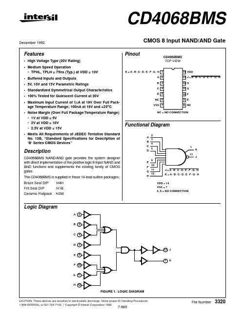
CAUTION: These devices are sensitive to electrostatic discharge; follow proper IC Handling Procedures.CD4068BMSCMOS 8 Input NAND/AND GatePinoutCD4068BMS TOP VIEWFunctional DiagramK =A · B · C · D · E · F · G · H A B C D NC VSS VDDJ =A · B · C · D · E · F · G · H H G F E NC1234567141312111098NC = NO CONNECTION12111092345A B C DE F G H13JK 1J =A · B · C · D · E · F · G · H K =A · B · C · D · E · F · G · H VDD = 14VSS = 76, 8 = NO CONNECTIONFeatures•High Voltage Type (20V Rating)•Medium Speed Operation-TPHL, TPLH = 75ns (Typ.) at VDD = 10V •Buffered Inputs and Outputs •5V, 10V and 15V Parametric Ratings•Standardized Symmetrical Output Characteristics •100% Tested for Quiescent Current at 20V•Maximum Input Current of 1µA at 18V Over Full Pack-age Temperature Range; 100nA at 18V and +25o C •Noise Margin (Over Full Package/Temperature Range)-1V at VDD = 5V -2V at VDD = 10V - 2.5V at VDD = 15V •Meets All Requirements of JEDEC Tentative Standard No. 13B, “Standard Specifications for Description of ‘B’ Series CMOS Devices”DescriptionCD4068BMS NAND/AND gate provides the system designer with direct implementation of the positive logic 8 Input NAND and AND functions and supplements the existing family of CMOS gates.The CD4068BMS is supplied in these 14 lead outline packages:Braze Seal DIP H4H Frit Seal DIPH1B Ceramic FlatpackH3WDecember 1992Logic DiagramFIGURE 1.LOGIC DIAGRAM13J1K2A 3B4C 5D 9E 10F 11G 12H File Number3320Absolute Maximum Ratings Reliability InformationDC Supply Voltage Range, (VDD) . . . . . . . . . . . . . . .-0.5V to +20V (Voltage Referenced to VSS Terminals)Input Voltage Range, All Inputs . . . . . . . . . . . . .-0.5V to VDD +0.5V DC Input Current, Any One Input . . . . . . . . . . . . . . . . . . . . . . . .±10mA Operating Temperature Range. . . . . . . . . . . . . . . .-55o C to +125o C Package Types D, F, K, HStorage Temperature Range (TSTG). . . . . . . . . . .-65o C to +150o C Lead Temperature (During Soldering) . . . . . . . . . . . . . . . . .+265o C At Distance 1/16 ± 1/32 Inch (1.59mm± 0.79mm) from case for 10s Maximum Thermal Resistance . . . . . . . . . . . . . . . .θjaθjc Ceramic DIP and FRIT Package. . . . .80o C/W20o C/W Flatpack Package . . . . . . . . . . . . . . . .70o C/W20o C/W Maximum Package Power Dissipation (PD) at +125o CFor TA = -55o C to +100o C (Package Type D, F, K). . . . . .500mW For TA = +100o C to +125o C (Package Type D, F, K) . . . . .DerateLinearity at 12mW/o C to 200mW Device Dissipation per Output Transistor . . . . . . . . . . . . . . .100mW For TA = Full Package Temperature Range (All Package Types) Junction Temperature . . . . . . . . . . . . . . . . . . . . . . . . . . . . . .+175o CTABLE1.DC ELECTRICAL PERFORMANCE CHARACTERISTICSPARAMETER SYMBOL CONDITIONS(NOTE 1)GROUP ASUBGROUPS TEMPERATURELIMITSUNITSMIN MAXSupply Current IDD VDD = 20V, VIN = VDD or GND1+25o C-0.5µA2+125o C-50µAVDD = 18V, VIN = VDD or GND3-55o C-0.5µA Input Leakage Current IIL VIN = VDD or GND VDD = 201+25o C-100-nA2+125o C-1000-nAVDD = 18V3-55o C-100-nA Input Leakage Current IIH VIN = VDD or GND VDD = 201+25o C-100nA2+125o C-1000nAVDD = 18V3-55o C-100nA Output Voltage VOL15VDD = 15V, No Load1, 2, 3+25o C, +125o C, -55o C-50mV Output Voltage VOH15VDD = 15V, No Load (Note 3)1, 2, 3+25o C, +125o C, -55o C14.95-V Output Current (Sink)IOL5VDD = 5V, VOUT = 0.4V1+25o C0.53-mA Output Current (Sink)IOL10VDD = 10V, VOUT = 0.5V1+25o C 1.4-mA Output Current (Sink)IOL15VDD = 15V, VOUT = 1.5V1+25o C 3.5-mA Output Current (Source)IOH5A VDD = 5V, VOUT = 4.6V1+25o C--0.53mA Output Current (Source)IOH5B VDD = 5V, VOUT = 2.5V1+25o C--1.8mA Output Current (Source)IOH10VDD = 10V, VOUT = 9.5V1+25o C--1.4mA Output Current (Source)IOH15VDD = 15V, VOUT = 13.5V1+25o C--3.5mA N Threshold Voltage VNTH VDD = 10V, ISS = -10µA1+25o C-2.8-0.7V P Threshold Voltage VPTH VSS = 0V, IDD = 10µA1+25o C0.7 2.8VFunctional F VDD = 2.8V, VIN = VDD or GND7+25o C VOH >VDD/2VOL <VDD/2VVDD = 20V, VIN = VDD or GND7+25o CVDD = 18V, VIN = VDD or GND8A+125o CVDD = 3V, VIN = VDD or GND8B-55o CInput Voltage Low(Note 2)VIL VDD = 5V, VOH > 4.5V, VOL < 0.5V1, 2, 3+25o C, +125o C, -55o C- 1.5VInput Voltage High(Note 2)VIH VDD = 5V, VOH > 4.5V, VOL < 0.5V1, 2, 3+25o C, +125o C, -55o C 3.5-VInput Voltage Low (Note 2)VIL VDD = 15V, VOH > 13.5V,VOL < 1.5V1, 2, 3+25o C, +125o C, -55o C-4VInput Voltage High (Note 2)VIH VDD = 15V, VOH > 13.5V,VOL < 1.5V1, 2, 3+25o C, +125o C, -55o C11-VNOTES: 1.All voltages referenced to device GND, 100% testing being implemented.2.Go/No Go test with limits applied to inputs.3.For accuracy, voltage is measured differentially to VDD. Limitis 0.050V max.TABLE2.AC ELECTRICAL PERFORMANCE CHARACTERISTICSPARAMETER SYMBOL CONDITIONS(NOTES 1, 2)GROUP ASUBGROUPS TEMPERATURELIMITSUNITSMIN MAXPropagation Delay TPHLTPLH VDD = 5V, VIN = VDD or GND9+25o C-300ns10, 11+125o C, -55o C-405nsTransition Time TTHLTTLH VDD = 5V, VIN = VDD or GND9+25o C-200ns10, 11+125o C, -55o C-270nsNOTES:1.CL = 50pF, RL = 200K, Input TR, TF < 20ns.2.-55o C and +125o C limits guaranteed, 100% testing being implemented.TABLE3.ELECTRICAL PERFORMANCE CHARACTERISTICSPARAMETER SYMBOL CONDITIONS NOTES TEMPERATURELIMITSUNITS MIN MAXSupply Current IDD VDD = 5V, VIN = VDD or GND1, 2-55o C, +25o C-0.25µA+125o C-7.5µAVDD = 10V, VIN = VDD or GND1, 2-55o C, +25o C-0.5µA+125o C-15µAVDD = 15V, VIN = VDD or GND1, 2-55o C, +25o C-0.5µA+125o C-30µA Output Voltage VOL VDD = 5V, No Load1, 2+25o C, +125o C,-55o C-50mVOutput Voltage VOL VDD = 10V, No Load1, 2+25o C, +125o C,-55o C-50mVOutput Voltage VOH VDD = 5V, No Load1, 2+25o C, +125o C,-55o C4.95-VOutput Voltage VOH VDD = 10V, No Load1, 2+25o C, +125o C,-55o C9.95-V Output Current (Sink)IOL5VDD = 5V, VOUT = 0.4V1, 2+125o C0.36-mA-55o C0.64-mA Output Current (Sink)IOL10VDD = 10V, VOUT = 0.5V1, 2+125o C0.9-mA-55o C 1.6-mA Output Current (Sink)IOL15VDD = 15V, VOUT = 1.5V1, 2+125o C 2.4-mA-55o C 4.2-mA Output Current (Source)IOH5A VDD = 5V, VOUT = 4.6V1, 2+125o C--0.36mA-55o C--0.64mA Output Current (Source)IOH5B VDD = 5V, VOUT = 2.5V1, 2+125o C--1.15mA-55o C--2.0mA Output Current (Source)IOH10VDD = 10V, VOUT = 9.5V1, 2+125o C--0.9mA-55o C--2.6mA Output Current (Source)IOH15VDD =15V, VOUT = 13.5V1, 2+125o C--2.4mA-55o C--4.2mAInput Voltage Low VIL VDD = 10V, VOH > 9V, VOL <1V 1, 2+25o C, +125o C,-55o C-3VInput Voltage High VIH VDD = 10V, VOH > 9V, VOL <1V 1, 2+25o C, +125o C,-55o C7-V Propagation DelayTPHL TPLH VDD = 10V 1, 2, 3+25o C -150ns VDD = 15V 1, 2, 3+25o C -110ns Transition TimeTTHLVDD = 10V 1, 2, 3+25o C -100ns VDD = 15V1, 2, 3+25o C -80ns Input Capacitance CINAny Input1, 2+25o C-7.5pFNOTES:1.All voltages referenced to device GND.2.The parameters listed on Table 3 are controlled via design or process and are not directly tested. These parameters are characterized on initial design release and upon design changes which would affect these characteristics.3.CL = 50pF, RL = 200K, Input TR, TF < 20ns.TABLE 4.POST IRRADIATION ELECTRICAL PERFORMANCE CHARACTERISTICSPARAMETER SYMBOL CONDITIONSNOTES TEMPERATURELIMITSUNITS MIN MAX Supply Current IDD VDD = 20V, VIN = VDD or GND 1, 4+25o C - 2.5µA N Threshold Voltage VNTH VDD = 10V, ISS = -10µA 1, 4+25o C -2.8-0.2V N Threshold Voltage Delta∆VTN VDD = 10V, ISS = -10µA 1, 4+25o C -±1V P Threshold Voltage VTP VSS = 0V, IDD = 10µA 1, 4+25o C 0.2 2.8V P Threshold Voltage Delta ∆VTP VSS = 0V, IDD = 10µA1, 4+25o C -±1V FunctionalFVDD = 18V, VIN = VDD or GND 1+25o CVOH >VDD/2VOL <VDD/2VVDD = 3V, VIN = VDD or GNDPropagation Delay TimeTPHL TPLHVDD = 5V1, 2, 3, 4+25o C- 1.35 x +25o C LimitnsNOTES: 1.All voltages referenced to device GND.2.CL = 50pF, RL = 200K, Input TR, TF < 20ns.3.See Table 2 for +25o C limit.4.Read and RecordTABLE 5.BURN-IN AND LIFE TEST DELTA PARAMETERS +25O C PARAMETERSYMBOL DELTA LIMITSupply Current - SSI IDD ±0.1µAOutput Current (Sink)IOL5± 20% x Pre-Test Reading Output Current (Source)IOH5A± 20% x Pre-Test ReadingTABLE 6.APPLICABLE SUBGROUPSCONFORMANCE GROUP MIL-STD-883METHOD GROUP A SUBGROUPSREAD AND RECORD Initial Test (Pre Burn-In)100% 50041, 7, 9IDD, IOL5, IOH5A Interim Test 1 (Post Burn-In)100% 50041, 7, 9IDD, IOL5, IOH5ATABLE 3.ELECTRICAL PERFORMANCE CHARACTERISTICS (Continued)PARAMETER SYMBOL CONDITIONSNOTES TEMPERATURE LIMITSUNITS MIN MAXInterim Test 2 (Post Burn-In)100% 50041, 7, 9IDD, IOL5, IOH5APDA (Note 1)100% 50041, 7, 9, DeltasInterim Test 3 (Post Burn-In)100% 50041, 7, 9IDD, IOL5, IOH5APDA (Note 1)100% 50041, 7, 9, Deltas Final Test 100% 50042, 3, 8A, 8B, 10, 11Group A Sample 50051, 2, 3, 7, 8A, 8B, 9, 10, 11Group BSubgroup B-5Sample 50051, 2, 3, 7, 8A, 8B, 9, 10, 11, DeltasSubgroups 1, 2, 3, 9, 10, 11Subgroup B-6Sample 50051, 7, 9Group DSample 50051, 2, 3, 8A, 8B, 9Subgroups 1, 2 3NOTE:1. 5% Parameteric, 3% Functional; Cumulative for Static 1 and 2.TABLE 7.TOTAL DOSE IRRADIATIONCONFORMANCE GROUPS MIL-STD-883METHODTESTREAD AND RECORD PRE-IRRAD POST-IRRAD PRE-IRRADPOST-IRRAD Group E Subgroup 250051, 7, 9Table 41, 9Table 4TABLE 8.BURN-IN AND IRRADIATION TEST CONNECTIONSFUNCTION OPEN GROUND VDD 9V ± -0.5VOSCILLATOR50kHz25kHzStatic Burn-In 1Note 11, 6, 8, 132-5, 7, 9-1214Static Burn-In 2Note 11, 6, 8, 1372-5, 9-12, 14Dynamic Burn-In Note 16, 87141, 132-5, 9-12Irradiation Note 21, 6, 8, 1372-5, 9-12, 14NOTE:1.Each pin except VDD and GND will have a series resistor of 10K ± 5%, VDD = 18V ± 0.5V2.Each pin except VDD and GND will have a series resistor of 47K ±5%; Group E, Subgroup 2, sample size is 4 dice/wafer, 0 failures, VDD = 10V ± 0.5VTABLE 6.APPLICABLE SUBGROUPSCONFORMANCE GROUP MIL-STD-883METHOD GROUP A SUBGROUPSREAD AND RECORDSchematicFIGURE 2.SCHEMATIC DIAGRAM1112109*nnnnpppp***VSSppnnVSSnp VSS VDDVDDnp13npVSSVDD1npVSSVDD3245*nnnnpppp***VDD VDDALL INPUTS PROTECTED BY *CMOS PROTECTION NETWORKVDDVSSDETAIL OF INVERTERSINVERTERSTypical Performance CharacteristicsFIGURE 3.TYPICAL OUTPUT LOW (SINK) CURRENTCHARACTERISTICSFIGURE 4.MINIMUM OUTPUT LOW (SINK) CURRENTCHARACTERISTICSFIGURE 5.TYPICAL OUTPUT HIGH (SOURCE) CURRENTCHARACTERISTICS FIGURE 6.MINIMUM OUTPUT HIGH (SOURCE) CURRENTCHARACTERISTICSFIGURE 7.TYPICAL TRANSITION TIME AS A FUNCTION OFLOAD CAPACITANCE FIGURE 8.TYPICAL PROPAGATION DELAY TIME AS AFUNCTION OF LOAD CAPACITANCE10V5V AMBIENT TEMPERATURE (T A ) = +25o CGATE-TO-SOURCE VOLTAGE (VGS) = 15V51015151********DRAIN-TO-SOURCE VOLTAGE (VDS) (V)O U T P U T L O W (S I N K ) C U R R E N T (I O L ) (m A )10V5VAMBIENT TEMPERATURE (T A ) = +25o CGATE-TO-SOURCE VOLTAGE (VGS) = 15V510157.55.02.510.012.515.0DRAIN-TO-SOURCE VOLTAGE (VDS) (V)O U T P U T L O W (S I N K ) C U R R E N T (I O L ) (m A )-10V-15VAMBIENT TEMPERATURE (T A ) = +25oCGATE-TO-SOURCE VOLTAGE (VGS) = -5V0-5-10-15DRAIN-TO-SOURCE VOLTAGE (VDS) (V)-20-25-30-5-10-15O U T P U T H I G H (S O U R C E ) C U R R E N T (I O H ) (m A )-10V-15VAMBIENT TEMPERATURE (T A ) = +25o C-5-10-15DRAIN-TO-SOURCE VOLTAGE (VDS) (V)-5-10-15O U T P U T H I G H (S O U R C E ) C U R R E N T (I O H ) (m A )GATE-TO-SOURCE VOLTAGE (VGS) = -5VAMBIENT TEMPERATURE (T A ) = +25o CLOAD CAPACITANCE (CL) (pF)40608010020050100150200SUPPL Y VOLTAGE (VDD) = 5V10V15VT R A N S I T I O N T I M E (t T H L , t T L H ) (n s )LOAD CAPACITANCE (CL) (pF)0251020304050607080901005075100125150175P R O P A G A T I O N D E L A Y T I M E (t P H L , t P L H ) (n s )10V 15VAMBIENT TEMPERATURE (T A ) = +25o CSUPPL Y VOLTAGE (VDD) = 5VAll Intersil semiconductor products are manufactured, assembled and tested under ISO9000 quality systems certification.Intersil products are sold by description only. Intersil Corporation reserves the right to make changes in circuit design and/or specifications at any time without notice. Accordingly, the reader is cautioned to verify that data sheets are current before placing orders. Information furnished by Intersil is believed to be accurate and reliable. However, no responsibility is assumed by Intersil or its subsidiaries for its use; nor for any infringements of patents or other rights of third parties which may result from its use. No license is granted by implication or otherwise under any patent or patent rights of Intersil or its subsidiaries.For information regarding Intersil Corporation and its products, see web site FIGURE 9.TYPICAL VOLTAGE TRANSFERCHARACTERISTICS (NAND OUTPUT)FIGURE 10.TYPICAL DYNAMIC POWER DISSIPATION AS AFUNCTION OF FREQUENCYChip Dimensions and Pad LayoutDimensions in parenthesis are in millimeters and are derived from the basic inch dimensions as indicated.Grid graduations are in mils (10-3 inch).METALLIZATION:Thickness: 11k Å−14k Å, AL.PASSIVATION:10.4kÅ - 15.6k Å, SilaneBOND PADS:0.004 inches X 0.004 inches MIN DIE THICKNESS:0.0198 inches - 0.0218 inchesTypical Performance Characteristics(Continued)AMBIENT TEMPERATURE (T A ) = +25o CSUPPLY VOLTAGE (VDD) = 15V 10V5V 15105510152025INPUT VOLTAGE (VI) (V)O U T P U T V O L T A G E (V O ) (V )CL = 15pFCL = 50pF 10V 5V10V AMBIENT TEMPERATURE (T A ) = +25oC SUPPLY VOLTAGE (VDD) = 15V 10510310P O W E R D I S S I P A T I O N (P D ) (µW )102104INPUT FREQUENCY (fI) (kHz)110102103104(O N E O U T P U T L O A D E D )86428642864286428642864286428642。
CD4063BPWG4中文资料

Data sheet acquired from Harris Semiconductor SCHS050C − Revised October 2003The CD4063B types are supplied in 16-lead hermetic dual-in-line ceramic packages (F3A suffix), 16-lead dual-in-line plastic packages (E suffix), 16-lead small-outline packages (M, M96, MT, and NSR suffixes), and 16-lead thin shrink small-outline packages (PW and PWR suffixes). This device is pin-compatible with the standard 7485 TTL type.IMPORTANT NOTICETexas Instruments Incorporated and its subsidiaries(TI)reserve the right to make corrections,modifications,enhancements, improvements,and other changes to its products and services at any time and to discontinue any product or service without notice. Customers should obtain the latest relevant information before placing orders and should verify that such information is current and complete.All products are sold subject to TI’s terms and conditions of sale supplied at the time of order acknowledgment.TI warrants performance of its hardware products to the specifications applicable at the time of sale in accordance with TI’s standard warranty.Testing and other quality control techniques are used to the extent TI deems necessary to support this warranty.Except where mandated by government requirements,testing of all parameters of each product is not necessarily performed.TI assumes no liability for applications assistance or customer product design.Customers are responsible for their products and applications using TI components.To minimize the risks associated with customer products and applications,customers should provide adequate design and operating safeguards.TI does not warrant or represent that any license,either express or implied,is granted under any TI patent right,copyright,mask work right,or other TI intellectual property right relating to any combination,machine,or process in which TI products or services are rmation published by TI regarding third-party products or services does not constitute a license from TI to use such products or services or a warranty or endorsement e of such information may require a license from a third party under the patents or other intellectual property of the third party,or a license from TI under the patents or other intellectual property of TI. Reproduction of information in TI data books or data sheets is permissible only if reproduction is without alteration and is accompanied by all associated warranties,conditions,limitations,and notices.Reproduction of this information with alteration is an unfair and deceptive business practice.TI is not responsible or liable for such altered documentation.Resale of TI products or services with statements different from or beyond the parameters stated by TI for that product or service voids all express and any implied warranties for the associated TI product or service and is an unfair and deceptive business practice.TI is not responsible or liable for any such statements.TI products are not authorized for use in safety-critical applications(such as life support)where a failure of the TI product would reasonably be expected to cause severe personal injury or death,unless officers of the parties have executed an agreement specifically governing such use.Buyers represent that they have all necessary expertise in the safety and regulatory ramifications of their applications,and acknowledge and agree that they are solely responsible for all legal,regulatory and safety-related requirements concerning their products and any use of TI products in such safety-critical applications,notwithstanding any applications-related information or support that may be provided by TI.Further,Buyers must fully indemnify TI and its representatives against any damages arising out of the use of TI products in such safety-critical applications.TI products are neither designed nor intended for use in military/aerospace applications or environments unless the TI products are specifically designated by TI as military-grade or"enhanced plastic."Only products designated by TI as military-grade meet military specifications.Buyers acknowledge and agree that any such use of TI products which TI has not designated as military-grade is solely at the Buyer's risk,and that they are solely responsible for compliance with all legal and regulatory requirements in connection with such use.TI products are neither designed nor intended for use in automotive applications or environments unless the specific TI products are designated by TI as compliant with ISO/TS16949requirements.Buyers acknowledge and agree that,if they use anynon-designated products in automotive applications,TI will not be responsible for any failure to meet such requirements. Following are URLs where you can obtain information on other Texas Instruments products and application solutions:Products ApplicationsAmplifiers AudioData Converters AutomotiveDSP BroadbandInterface Digital ControlLogic MilitaryPower Mgmt Optical NetworkingMicrocontrollers SecurityLow Power TelephonyWirelessVideo&ImagingWirelessMailing Address:Texas Instruments,Post Office Box655303,Dallas,Texas75265Copyright©2007,Texas Instruments IncorporatedPACKAGING INFORMATIONOrderable Device Status(1)PackageType PackageDrawingPins PackageQtyEco Plan(2)Lead/Ball Finish MSL Peak Temp(3)CD4063BE ACTIVE PDIP N1625Pb-Free(RoHS)CU NIPDAU N/A for Pkg TypeCD4063BEE4ACTIVE PDIP N1625Pb-Free(RoHS)CU NIPDAU N/A for Pkg Type CD4063BF ACTIVE CDIP J161TBD A42SNPB N/A for Pkg Type CD4063BF3A ACTIVE CDIP J161TBD A42SNPB N/A for Pkg Type CD4063BM ACTIVE SOIC D1640Green(RoHS&no Sb/Br)CU NIPDAU Level-1-260C-UNLIMCD4063BM96ACTIVE SOIC D162500Green(RoHS&no Sb/Br)CU NIPDAU Level-1-260C-UNLIMCD4063BM96E4ACTIVE SOIC D162500Green(RoHS&no Sb/Br)CU NIPDAU Level-1-260C-UNLIMCD4063BM96G4ACTIVE SOIC D162500Green(RoHS&no Sb/Br)CU NIPDAU Level-1-260C-UNLIMCD4063BME4ACTIVE SOIC D1640Green(RoHS&no Sb/Br)CU NIPDAU Level-1-260C-UNLIMCD4063BMG4ACTIVE SOIC D1640Green(RoHS&no Sb/Br)CU NIPDAU Level-1-260C-UNLIMCD4063BMT ACTIVE SOIC D16250Green(RoHS&no Sb/Br)CU NIPDAU Level-1-260C-UNLIMCD4063BMTE4ACTIVE SOIC D16250Green(RoHS&no Sb/Br)CU NIPDAU Level-1-260C-UNLIMCD4063BMTG4ACTIVE SOIC D16250Green(RoHS&no Sb/Br)CU NIPDAU Level-1-260C-UNLIMCD4063BNSR ACTIVE SO NS162000Green(RoHS&no Sb/Br)CU NIPDAU Level-1-260C-UNLIMCD4063BNSRE4ACTIVE SO NS162000Green(RoHS&no Sb/Br)CU NIPDAU Level-1-260C-UNLIMCD4063BNSRG4ACTIVE SO NS162000Green(RoHS&no Sb/Br)CU NIPDAU Level-1-260C-UNLIMCD4063BPW ACTIVE TSSOP PW1690Green(RoHS&no Sb/Br)CU NIPDAU Level-1-260C-UNLIMCD4063BPWE4ACTIVE TSSOP PW1690Green(RoHS&no Sb/Br)CU NIPDAU Level-1-260C-UNLIMCD4063BPWG4ACTIVE TSSOP PW1690Green(RoHS&no Sb/Br)CU NIPDAU Level-1-260C-UNLIMCD4063BPWR ACTIVE TSSOP PW162000Green(RoHS&no Sb/Br)CU NIPDAU Level-1-260C-UNLIMCD4063BPWRE4ACTIVE TSSOP PW162000Green(RoHS&no Sb/Br)CU NIPDAU Level-1-260C-UNLIMCD4063BPWRG4ACTIVE TSSOP PW162000Green(RoHS&no Sb/Br)CU NIPDAU Level-1-260C-UNLIM(1)The marketing status values are defined as follows:ACTIVE:Product device recommended for new designs.LIFEBUY:TI has announced that the device will be discontinued,and a lifetime-buy period is in effect.NRND:Not recommended for new designs.Device is in production to support existing customers,but TI does not recommend using this part in a new design.PREVIEW:Device has been announced but is not in production.Samples may or may not be available.OBSOLETE:TI has discontinued the production of the device.(2)Eco Plan-The planned eco-friendly classification:Pb-Free(RoHS),Pb-Free(RoHS Exempt),or Green(RoHS&no Sb/Br)-please check /productcontent for the latest availability information and additional product content details.TBD:The Pb-Free/Green conversion plan has not been defined.Pb-Free(RoHS):TI's terms"Lead-Free"or"Pb-Free"mean semiconductor products that are compatible with the current RoHS requirements for all6substances,including the requirement that lead not exceed0.1%by weight in homogeneous materials.Where designed to be soldered at high temperatures,TI Pb-Free products are suitable for use in specified lead-free processes.Pb-Free(RoHS Exempt):This component has a RoHS exemption for either1)lead-based flip-chip solder bumps used between the die and package,or2)lead-based die adhesive used between the die and leadframe.The component is otherwise considered Pb-Free(RoHS compatible)as defined above.Green(RoHS&no Sb/Br):TI defines"Green"to mean Pb-Free(RoHS compatible),and free of Bromine(Br)and Antimony(Sb)based flame retardants(Br or Sb do not exceed0.1%by weight in homogeneous material)(3)MSL,Peak Temp.--The Moisture Sensitivity Level rating according to the JEDEC industry standard classifications,and peak solder temperature.Important Information and Disclaimer:The information provided on this page represents TI's knowledge and belief as of the date that it is provided.TI bases its knowledge and belief on information provided by third parties,and makes no representation or warranty as to the accuracy of such information.Efforts are underway to better integrate information from third parties.TI has taken and continues to take reasonable steps to provide representative and accurate information but may not have conducted destructive testing or chemical analysis on incoming materials and chemicals.TI and TI suppliers consider certain information to be proprietary,and thus CAS numbers and other limited information may not be available for release.In no event shall TI's liability arising out of such information exceed the total purchase price of the TI part(s)at issue in this document sold by TI to Customer on an annual basis.TAPE AND REEL INFORMATION*All dimensions are nominalDevicePackage Type Package Drawing Pins SPQReel Diameter (mm)Reel Width W1(mm)A0(mm)B0(mm)K0(mm)P1(mm)W (mm)Pin1Quadrant CD4063BM96SOIC D 162500330.016.4 6.510.3 2.18.016.0Q1CD4063BNSR SO NS 162000330.016.48.210.5 2.512.016.0Q1CD4063BPWRTSSOPPW162000330.012.47.05.61.68.012.0Q1*All dimensions are nominalDevice Package Type Package Drawing Pins SPQ Length(mm)Width(mm)Height(mm) CD4063BM96SOIC D162500333.2345.928.6 CD4063BNSR SO NS162000346.0346.033.0 CD4063BPWR TSSOP PW162000346.0346.029.0。
CD4046中文资料_数据手册_参数

CD4046B型号采用16铅密封双线陶瓷封装(F3Asuffix)、16铅双线塑料封装(Esuffix)、16铅小外径封装(nsr后缀)和16铅薄收缩小外径封装 (PW和PWR后缀)(1)营销状态值定义如下:ACTIVE:推荐用于新设计的产品设备。LIFEBUY:德州仪器公司宣布该设备将停产,终身购买 期已经生效。NRND:不推荐用于新设计。该设备正在生产中,以支持现有客户,但TI不建议在新设计中使用该部件。预览:设备已宣 布,但尚未投产。样品可能有也可能没有。过时的:TI已经停止生产该设备。(2)Eco Plan—可能目前不可用—请查看以获得最新的可用 信息和额外的产品内容详细信息。没有:还没有可用的铅(Pb-Free)。无铅(RoHS): TI的术语“无铅”或“无铅”是指与所有6种物质的现 行RoHS要求兼容的半导体产品,包括在均质材料中铅的重量不超过0.1%的要求。CD4046设计用于高温焊接的无钛pb产品适用于特定 的无铅工艺。环保(RoHS &没有某人/ Br): TI定义“绿色”意味着“Pb-Free”,此外,使用包装材料,不含卤素,包括溴(Br)或锑(某人)总数的 0.1%以上产品的重量。(3)实验室,峰值温度。湿度敏感性级别评级根据JEDECindustry标准分类和soldertemperature峰值。重要信息和免 责声明:本页所提供的信息代表德州仪器自提供之日起的知识和信念。TI的知识和信念基于第三方提供的信息,对于这些信息的准确性 不作任何陈述或保证。目前正在努力更好地整合来自第三方的信息。TI已采取并将继续采取合理措施,提供具有代表性和准确的信 息,但可能未对来料和化学品进行破坏性测试或化学分析。TI和TI供应商认为某些信息是专有的,因此CAS号码和其他有限的信息可 能无法发布。在任何情况下,TI因该等信息而产生的责任都不应超过.CD4046客户在本文件中每年销售的TI部件的采购总价无铅 (RoHS): TI的术语“无铅”或“无铅”是指与当前所有6种物质的RoHS要求兼容的半导体产品,包括在均质材料中铅的重量不超过0.1% 的要求。设计用于高温焊接的无钛pb产品适用于特定的无铅工艺。无铅(免RoHS):该组件具有免RoHS的任何1)基于铅的倒装芯片焊料 凸点之间使用的模具和封装,或2)基于铅的模具胶粘剂之间使用的模具和铅框架。否则,该CD4046组件被认为是如上定义的无pb (RoHS兼容)的。绿色(RoHS & no Sb/Br):TI定义“绿色”意味着Pb-Free (RoHS兼容),和自由的溴(Br)和(某人)锑阻燃剂(Br或某人不超过 0.1% weightin均质材料)(3)实验室,峰值温度。湿度敏感性级别评级根据电平行业标准分类,和峰值焊接温度。(4)CD4046可能有额外的标 记,与标志,许多跟踪代码的信息,(5)多个设备标记将在括号内。只有一个设备标记包含在括号中,并以“~”分隔,将出现在一个设备 上。如果一条线是缩进的,那么它是前一条线的延续,这两条线代表了该设备的整个设备标记。Finish选项由一条垂直的直线分隔。如 果结束值超过最大列宽,则铅/球结束值可以绕成两行。重要信息和免责声明:本页所提供的信息代表德州仪器自提供之日起的知识和 信念。TI的知识和信念基于第三方提供的信息,对于这些信息的准确性不作任何陈述或保证。目前正在努力更好地整合来自第三方的 信息。TI已经并将继续采取合理措施,提供具有代表性和准确的信息,但可能没有对来料和化学品进行破坏性测试或化学分析。TI和 TI供应商认为某些信息是专有的,因此CAS编号和其他有限的信息可能无法发布。在任何情况下,TI因该等信息而产生的责任,都不 应超过TI在本文件中每年向客户出售的TI务,只售 原装现货库存,万联芯城电子元器件全国供应,专为终端生产, 研发企业提供现货物料,价格优势明显,BOM配单采购可节省 逐个搜索购买环节,只需提交BOM物料清单,商城即可为您报 价,万联芯城完善的供应链体系能够满足多种报价需求,为客 户节省成本,点击进入万联芯城。
CD4070BPWRG4中文资料

2
元器件交易网
CD4070B, CD4077B
VDD
B†
2(5, 9, 12)
A†
1(6, 8, 13)
p
nn
VSS
p
VDD
p
n
VSS
VDD
† INPUTS PROTECTED
BY CMOS PROTECTION
NETWORK
VDD
VDD
p
B†
p
p
2(5, 9, 12)
Package Thermal Impedance, θJA (see Note 1): E (PDIP) Package . . . . . . . . . . . . . . . . . . . . . . . . . . . . . . . 80oC/W M (SOIC) Package. . . . . . . . . . . . . . . . . . . . . . . . . . . . . . . 86oC/W NS (SOP) Package . . . . . . . . . . . . . . . . . . . . . . . . . . . . . . 76oC/W PW (TSSOP) Package . . . . . . . . . . . . . . . . . . . . . . . . . 113oC/W
Package Temperature Range - 100nA at 18V and 25oC
• Noise Margin (Over Full Package Temperature Range) - 1V at VDD = 5V, 2V at VDD = 10V, 2.5V at VDD = 15V
IC集成电路型号大全及40系列芯片功能大全
CD4000 双3输入端或非门单非门CD4001 四2输入端或非门CD4002 双4输入端或非门CD4006 18位串入/串出移位存放器CD4007 双互补对加反相器CD4008 4位超前进位全加器CD4009 六反相缓冲/变换器CD4010 六同相缓冲/变换器CD4011 四2输入端与非门CD4012 双4输入端与非门CD4013 双主-从D型触发器CD4014 8位串入/并入-串出移位存放器CD4015 双4位串入/并出移位存放器CD4016 四传输门CD4017 十进制计数/分配器CD4018 可预制1/N计数器CD4019 四与或选择器CD4020 14级串行二进制计数/分频器CD4021 08位串入/并入-串出移位存放器CD4022 八进制计数/分配器CD4023 三3输入端与非门CD4024 7级二进制串行计数/分频器CD4025 三3输入端或非门CD4026 十进制计数/7段译码器CD4027 双J-K触发器CD4028 BCD码十进制译码器CD4029 可预置可逆计数器CD4030 四异或门CD4031 64位串入/串出移位存储器CD4032 三串行加法器CD4033 十进制计数/7段译码器CD4034 8位通用总线存放器CD4035 4位并入/串入-并出/串出移位存放CD4038 三串行加法器CD4040 12级二进制串行计数/分频器CD4041 四同相/反相缓冲器CD4042 四锁存D型触发器CD4043 三态R-S锁存触发器("1"触发) CD4044 四三态R-S锁存触发器("0"触发) CD4046 锁相环CD4047 无稳态/单稳态多谐振荡器CD4048 四输入端可扩展多功能门CD4049 六反相缓冲/变换器CD4050 六同相缓冲/变换器CD4051 八选一模拟开关CD4052 双4选1模拟开关CD4053 三组二路模拟开关CD4054 液晶显示驱动器CD4055 BCD-7段译码/液晶驱动器CD4056 液晶显示驱动器CD4059 “N〞分频计数器 NSC/TICD4060 14级二进制串行计数/分频器CD4063 四位数字比拟器CD4066 四传输门CD4067 16选1模拟开关CD4068 八输入端与非门/与门CD4069 六反相器CD4070 四异或门CD4071 四2输入端或门CD4072 双4输入端或门CD4073 三3输入端与门CD4075 三3输入端或门CD4076 四D存放器CD4077 四2输入端异或非门CD4078 8输入端或非门/或门CD4081 四2输入端与门CD4082 双4输入端与门CD4085 双2路2输入端与或非门CD4086 四2输入端可扩展与或非门CD4089 二进制比例乘法器CD4093 四2输入端施密特触发器CD4095 三输入端J-K触发器CD4096 三输入端J-K触发器CD4097 双路八选一模拟开关CD4098 双单稳态触发器CD4099 8位可寻址锁存器CD40100 32位左/右移位存放器CD40101 9位奇偶较验器CD40102 8位可预置同步BCD减法计数器CD40103 8位可预置同步二进制减法计数器CD40104 4位双向移位存放器CD40105 先入先出FI-FD存放器CD40106 六施密特触发器CD40107 双2输入端与非缓冲/驱动器CD40108 4字×4位多通道存放器CD40109 四低-高电平位移器CD40110 十进制加/减,计数,锁存,译码驱动CD40147 10-4线编码器CD40160 可预置BCD加计数器CD40161 可预置4位二进制加计数器CD40162 BCD加法计数器CD40163 4位二进制同步计数器CD40174 六锁存D型触发器CD40175 四D型触发器CD40181 4位算术逻辑单元/函数发生器CD40182 超前位发生器CD40192 可预置BCD加/减计数器(双时钟) CD40193 可预置4位二进制加/减计数器CD40194 4位并入/串入-并出/串出移位存放CD40195 4位并入/串入-并出/串出移位存放CD40208 4×4多端口存放器CD4501 4输入端双与门与2输入端或非门CD4502 可选通三态输出六反相/缓冲器CD4503 六同相三态缓冲器CD4504 六电压转换器CD4506 双二组2输入可扩展或非门CD4508 双4位锁存D型触发器CD4510 可预置BCD码加/减计数器CD4511 BCD锁存,7段译码,驱动器CD4512 八路数据选择器CD4513 BCD锁存,7段译码,驱动器(消隐) CD4514 4位锁存,4线-16线译码器CD4515 4位锁存,4线-16线译码器CD4516 可预置4位二进制加/减计数器CD4517 双64位静态移位存放器CD4518 双BCD同步加计数器CD4519 四位与或选择器CD4520 双4位二进制同步加计数器CD4521 24级分频器CD4522 可预置BCD同步1/N计数器CD4526 可预置4位二进制同步1/N计数器CD4527 BCD比例乘法器CD4528 双单稳态触发器CD4529 双四路/单八路模拟开关CD4530 双5输入端优势逻辑门CD4531 12位奇偶校验器CD4532 8位优先编码器CD4536 可编程定时器CD4538 精细双单稳CD4539 双四路数据选择器CD4541 可编程序振荡/计时器CD4543 BCD七段锁存译码,驱动器CD4544 BCD七段锁存译码,驱动器CD4547 BCD七段译码/大电流驱动器CD4549 函数近似存放器CD4551 四2通道模拟开关CD4553 三位BCD计数器CD4555 双二进制四选一译码器/别离器CD4556 双二进制四选一译码器/别离器CD4558 BCD八段译码器CD4560 "N"BCD加法器CD4561 "9"求补器CD4573 四可编程运算放大器CD4574 四可编程电压比拟器CD4575 双可编程运放/比拟器CD4583 双施密特触发器CD4584 六施密特触发器CD4585 4位数值比拟器CD4599 8位可寻址锁存器CD22100 4×4×1交叉点开关0206A 天线开关集成电路03VFG9 发射压控振荡集成电路1021AC 发射压控振荡集成电路1097C 升压集成电路140N 电源取样比拟放大集成电路14DN363 伺服控制集成电路15105 充电控制集成电路15551 管理卡升压集成电路1710 视频信号处理集成电路1N706 混响延时集成电路20810-F6096 存储集成电路2252B 微处理集成电路2274 延迟集成电路24C01ACEA 存储集成电路24C026 存储集成电路24C04 存储集成电路24C64 码片集成电路24LC16B 存储集成电路24LC65 电可改写编程只读存储集成电路27C1000PC-12 存储集成电路27C2000QC-90 存储集成电路27C20T 存储集成电路27C512 电可改写编程只读存储集成电路2800 红外遥控信号接收集成电路28BV64 码片集成电路28F004 版本集成电路31085 射频电源集成电路32D54 电源、音频信号处理集成电路1732D75 电源、音频信号处理集成电路32D92 电源中频放大集成电路4066B 电子开关切换集成电路4094 移位存放串入、并出集成电路424260SDJ 存储集成电路4260 动态随机存储集成电路4270351/91B9905 中频放大集成电路4370341/90M9919 中频处理集成电路4464 存储集成电路4558 双运算放大集成电路4580D 双运算放大集成电路47C1638AN-U337 微处理集成电路47C1638AU-353 微处理集成电路47C432GP 微处理集成电路47C433AN-3888 微处理集成电路49/4CR1A 中频放大集成电路5101 天线开关集成电路5G052 发光二极管四位显示驱动集成电路5G24 运算放大集成电路5W01 双运算放大集成电路649/CRIA70612 中频放大集成电路673/3CR2A 多模转换集成电路74122 可重触发单稳态集成电路74HC04 逻辑与非门集成电路74HC04D 六反相集成电路74HC123 单稳态集成电路74HC125 端口功能扩展集成电路74HC14N 六反相集成电路74HC157A 多路转换集成电路74HC165 移相存放集成电路1874HC245 总线收发集成电路74HC32 或门四2输入集成电路74HC374八D 触发集成电路74HC573D 存储集成电路74HCT157 多路转换双输入集成电路74HCT4046A 压控振荡集成电路74HCT4538D 单稳态集成电路74HCT4538N 触发脉冲集成电路74HCT86D 异或门四2输入集成电路74HCU04 与非门集成电路74LS125 端口功能扩展集成电路74LS373 锁存集成电路74LS393 计数双四位二进制集成电路74LS74双D 触发集成电路78014DFP 系统控制处理集成电路811N 伴音阻容偏置集成电路83D33 压控振荡集成电路85712 场扫描信号校正处理集成电路85713 行扫描信号校正集成电路87C52 微处理集成电路87CK38N-3584 微处理集成电路87CK38N-3627 微处理集成电路89C52 系统控制处理集成电路89C55 系统控制处理集成电路93C66 电可改写编程只读存储集成电路93LC56 电可改写编程存储集成电路9821K03 系统控制集成电路A1642P 背景歌声消除集成电路A701 红外遥控信号接收集成电路A7950 场频识别集成电路19A8772AN 色差信号延迟处理集成电路A9109 功率放大集成电路AAB 电源集成电路ACA650 色度信号解调集成电路ACFP2 色度、亮度信号别离集成电路ACP2371 多伴音、多语言改善集成电路ACVP2205 色度、亮度信号别离集成电路AD1853 立体声数/模转换集成电路AD1858 音频解调集成电路AD722 视频编码集成电路ADC2300E 音频数/模转换集成电路ADC2300J 音频数/模转换集成电路ADC2310E 音频数/模转换集成电路ADV7172 视频编码集成电路ADV7175A 视频编码集成电路AE31201 频率显示集成电路AJ7080 射频调制集成电路AK4321-VF-E1 音频数/模转换集成电路AN1319 双高速电压比拟集成电路AN1358S 双运算放大集成电路AN1393 双运算放大集成电路AN1431T 稳压电源集成电路AN1452 音频前置放大集成电路AN1458S 双运算放大集成电路AN206 伴音中频与前置放大集成电路AN222 自动频率控制集成电路AN236 副载波信号处理集成电路AN239Q 图像、伴音中频放大集成电路AN247P 图像中频放大、AGC控制集成电路AN253P 调频/调幅中频放大集成电路20AN262 音频前置放大集成电路AN2661NK 视频信号处理集成电路AN2663K 视频信号处理集成电路AN272 音频功率放大集成电路AN2751FAP 视频信号处理集成电路AN281 色度解码集成电路AN2870FC 多功能控制集成电路AN295 行、场扫描信号处理集成电路AN301 伺服控制集成电路AN305 视频自动增益控制集成电路AN306 色度自动相位控制集成电路AN318 直流伺服控制集成电路AN320 频率控制、调谐显示驱动集成电路AN3215K 视频信号处理集成电路AN3215S 视频信号处理集成电路AN3224K 磁头信号记录放大集成电路AN3248NK 亮度信号记录、重放处理集成电路AN331 视频信号处理集成电路AN3311K 磁头信号放大集成电路AN3313 磁头信号放大集成电路AN3321S 录像重放信号处理集成电路AN3331K 磁头信号处理集成电路AN3337NSB 磁头信号放大集成电路AN3380K 磁头信号处理集成电路AN3386NK 磁头信号处理集成电路AN3495K 色度、亮度信号降噪集成电路AN355 伴音中频放大、检波集成电路AN3581S 视频驱动集成电路AN366 调频/调幅中频放大集成电路AN3791 移位控制集成电路21AN3792 磁鼓伺服控制接口集成电路AN3795 主轴伺服控制接口集成电路AN3814K 电机驱动集成电路AN4265 音频功率放大集成电路AN4558 运算放大集成电路AN5010 电子选台集成电路AN5011 电子选台集成电路AN5015K 电子选台集成电路AN5020 红外遥控信号接收集成电路AN5025S 红外遥控信号接收集成电路AN5026K 红外遥控信号接收集成电路AN5031 电调谐控制集成电路AN5034 调谐控制集成电路AN5036 调谐控制集成电路AN5043 调谐控制集成电路AN5071 频段转换集成电路AN5095K 电视信号处理集成电路AN5110 图像中频放大集成电路AN5130 图像中频、视频检波放大集成电路AN5138NK 图像、伴音中频放大集成电路AN5156K 电视信号处理集成电路AN5177NK 图像、伴音中频放大集成电路AN5179K 图像、伴音中频放大集成电路AN5183K 中频信号处理集成电路AN5195K 中频、色度、扫描信号处理集成电路AN5215 伴音信号处理集成电路AN5520 伴音中频放大与鉴频集成电路AN5222 伴音中频放大集成电路AN5250 伴音中频放大、鉴频与功率放大集成电路AN5262 音频前置放大集成电路22AN5265 音频功率放大集成电路AN5270 音频功率放大集成电路AN5273 双声道音频功率放大集成电路AN5274 双声道音频功率放大集成电路AN5275 中置、3D放大集成电路AN5285K 双声道前置放大集成电路AN5295NK 音频信号切换集成电路AN5312 视频、色度信号处理集成电路AN5313NK 视频、色度信号处理集成电路AN5342 图像水平轮廓校正集成电路AN5342FB 水平清晰度控制集成电路AN5344FBP 色度信号处理集成电路AN5348K 人工智能信号处理集成电路AN5385K 色差信号放大集成电路AN5410 行、场扫描信号处理集成电路AN5421 同步检测集成电路AN5422 行、场扫描信号处理集成电路AN5512 场扫描输出集成电路AN5515 场扫描输出集成电路AN5521 场扫描输出集成电路AN5532 场扫描输出集成电路AN5534 场扫描输出集成电路AN5551 枕形校正集成电路AN5560 场频识别集成电路AN5600K 中频、亮度、色度与扫描信号处理集成电路AN5601K 视频、色度、同步信号处理集成电路AN5607K 视频、色度、行场扫描信号处理集成电路AN5615 视频信号处理集成电路AN5620X 色度信号处理集成电路AN5621 场扫描输出集成电路23AN5625 色度信号处理集成电路AN5633K 色度信号处理集成电路AN5635 色度解码集成电路AN5635NS 色度解码集成电路AN5637 色度解码、亮度延迟集成电路AN5650 同步信号别离集成电路AN5682K 基色电子开关切换集成电路AN5693K 视频、色度、行场扫描信号处理集成电路AN5712 图像中频放大、AGC控制集成电路AN5722 图像中频放大、检波集成电路AN5732 伴音中频放大、鉴频集成电路AN5743 音频功率放大集成电路AN5750 行自动频率控制与振荡集成电路AN5757S 行扫描电源电压控制集成电路AN5762 场扫描振荡、输出集成电路AN5764 光栅水平位置控制集成电路AN5765 电源稳压控制集成电路AN5767 同步信号处理集成电路AN5768 光栅倾斜校正控制集成电路AN5769 行、场会聚控制集成电路AN5790N 行扫描信号处理集成电路AN5791 同步脉冲相位与脉宽调整集成电路AN5803 双声道立体声解调集成电路AN5836 双声道前置放大集成电路AN5858K 视频信号控制集成电路AN5862 视频信号控制集成电路AN5862S-E1 视频信号开关控制集成电路AN5870K 模拟信号切换集成电路AN5891K 音频信号处理集成电路AN614 行枕形校正集成电路24AN6210 双声道前置放大集成电路AN6306S 亮度信号处理集成电路AN6308 模拟电子开关集成电路AN6327 视频重放信号处理集成电路AN6341N 伺服控制集成电路AN6342N 基准分频集成电路AN6344 伺服控制集成电路AN6345 分频集成电路AN6346N 磁鼓伺服控制集成电路AN6350 磁鼓伺服控制集成电路AN6357N 主轴接口集成电路AN6361N 色度信号处理集成电路AN6367NK 色度信号处理集成电路AN6371S 自动相位控制集成电路AN6387 电机伺服控制集成电路AN6550 卡拉OK音频放大集成电路AN6554 四运算放大集成电路AN6561 双运算放大集成电路AN6562SG 双运算放大集成电路AN6609N 电机驱动集成电路AN6612 电机稳速控制集成电路AN6650 电机速度控制集成电路AN6651 电机速度控制集成电路AN6652 电机稳速控制集成电路AN6875 发光二极管五位显示驱动集成电路AN6877 发光二极管七位显示驱动集成电路AN6884 发光二极管五位显示驱动集成电路AN6886 发光二极管五位显示驱动集成电路AN6888 发光二极管显示驱动集成电路AN6914 双电压比拟集成电路25AN7085N5 单片录、放音集成电路AN7105 双声道音频功率放大集成电路AN7106K 双声道音频功率放大集成电路AN7108 单片立体声放音集成电路AN710S 单片放音集成电路AN7110E 音频功率放大集成电路AN7114 音频功率放大集成电路AN7116 音频功率放大集成电路AN7118 双声道音频功率放大集成电路AN7118S 双声道音频功率放大集成电路AN7120 音频功率放大集成电路AN7124 双声道音频功率放大集成电路AN7145 双声道音频功率放大集成电路AN7148 双声道音频功率放大集成电路AN7158N 音频功率放大7.5W×2集成电路AN7161N 音频功率放大集成电路AN7164 双声道音频功率放大集成电路AN7171NK 音频功率放大集成电路AN7205 调频/调谐与高频放大集成电路AN7220 调频/调幅中频放大集成电路AN7222 调频/调幅中频放大集成电路AN7223 调频/调幅中频放大集成电路AN7226 调频/调幅中频放大集成电路AN7256 调频/调谐与中频放大集成电路AN7311 双声道前置放大集成电路AN7312 双声道前置放大集成电路AN7315 双声道前置放大集成电路AN7315S 双声道前置放大集成电路AN7320 音频前置放大集成电路AN7396K 双声道前置放大集成电路26AN7397K 双声道前置放大集成电路AN7410 调频立体声多路解码集成电路AN7414 调频立体声解码集成电路AN7420N 调频立体声解码集成电路AN7470 调频立体声解码集成电路AN7805 三端电源稳压+5V/1A集成电路AN7806 三端电源稳压+6V/1A集成电路AN7807 三端电源稳压+7V/1A集成电路AN7808 三端电源稳压+8V/1A集成电路AN7809 电源稳压+9V/1A集成电路AN7810 三端电源稳压+10V/1A集成电路AN7812 三端电源稳压+12V/1A集成电路AN7815 三端电源稳压+15V/1A集成电路AN7818 三端电源稳压+18V/1A集成电路AN7820 三端电源稳压+20V/1A集成电路AN7824 三端电源稳压+24V/1A集成电路AN78L05 三端电源稳压+5V/0.1A集成电路AN78L06 三端电源稳压+6V/0.1A集成电路AN78L08 三端电源稳压+8V/0.1A集成电路AN78L09 三端电源稳压+9V/0.1A集成电路AN78L10 三端电源稳压+10V/0.1A集成电路AN78L12 三端电源稳压+12V/0.1A集成电路AN78L15 三端电源稳压+15V/0.1A集成电路AN78L18 三端电源稳压+18V/0.1A集成电路AN78L20 三端电源稳压+20V/0.1A集成电路AN78L24 三端电源稳压+24V/0.1A集成电路AN78M05 三端电源稳压+5V/0.5A集成电路AN78M06 三端电源稳压+6V/0.5A集成电路AN78M08 三端电源稳压+8V/0.5A集成电路AN78M09 三端电源稳压+9V/0.5A集成电路27AN78M10 三端电源稳压+10V/0.5A集成电路AN78M12 三端电源稳压+12V/0.5A集成电路AN78M15 三端固定式稳压+15V/0.5A集成电路AN78M18 三端电源稳压+18V/0.5A集成电路AN78M20 三端电源稳压+20V/0.5A集成电路AN78M24 三端电源稳压+24V/0.5A集成电路AN7905 三端电源稳压-5V/1A集成电路AN7906 三端电源稳压-6V/1A集成电路AN7908T 三端电源稳压-8V/1A集成电路AN7909T 三端电源稳压-9V/1A集成电路AN7910T 三端电源稳压-10V/1A集成电路AN7912 三端电源稳压-12V/1A集成电路AN7915 三端电源稳压-15V/1A集成电路AN7918 三端电源稳压-18V/1A集成电路AN7920 三端电源稳压-20V/1A集成电路AN7924 三端电源稳压-24V/1A集成电路AN79L05 三端电源稳压-5V/0.1A集成电路AN79L06 三端电源稳压-6V/0.1A集成电路AN79L08 三端电源稳压-8V/0.1A集成电路AN79L09 三端电源稳压-9V/0.1A集成电路AN79L10 三端电源稳压-10V/0.1A集成电路AN79L12 三端电源稳压-12V/0.1A集成电路AN79L15 三端电源稳压-15V/0.1A集成电路AN79L18 三端电源稳压-18V/0.1A集成电路AN79L20 三端电源稳压-20V/0.1A集成电路AN79L24 三端电源稳压-24V/0.1A集成电路AN79M05 三端电源稳压-5V/0.5A集成电路AN79M06 三端电源稳压-6V/0.5A集成电路AN79M08 三端电源稳压-8V/0.5A集成电路AN79M09 三端电源稳压-9V/0.5A集成电路28AN79M10 三端电源稳压-10V/0.5A集成电路AN79M12 三端电源稳压-12V/0.5A集成电路AN79M15 三端电源稳压-15V/0.5A集成电路AN79M18 三端电源稳压-18V/0.5A集成电路AN79M20 三端电源稳压-20V/0.5A集成电路AN79M24 三端电源稳压-24V/0.5A集成电路AN8028 自激式开关电源控制集成电路AN8270K 主轴电机控制集成电路AN8280 电机驱动集成电路AN8281S 电机驱动集成电路AN8290S 主轴电机驱动集成电路AN8355S 条形码扫描接收集成电路AN8370S 光电伺服控制集成电路AN8373S 射频伺服处理集成电路AN8375S 伺服处理集成电路AN8389S-E1 电机驱动集成电路AN8480NSB 主轴电机驱动集成电路AN8481SB-E1 主轴电机驱动集成电路AN8482SB 主轴电机驱动集成电路AN8623FBQ 主轴伺服处理集成电路AN8788FB 电机驱动集成电路AN8802CE1V 伺服处理集成电路AN8813NSBS 主轴电机驱动集成电路AN8819NFB 伺服驱动、直流交换集成电路AN8824FBQ 前置放大集成电路AN8825NFHQ-V 聚焦、循迹误差处理集成电路AN8831SC 视频预视放集成电路AN8832SB-E1 射频放大、伺服处理集成电路AN8837SB-E1 伺服处理集成电路AN89C2051-24PC 微处理集成电路29APU2400U 音频信号处理集成电路APU2470 音频信号处理集成电路AS4C14405-60JC 动态随机存储1M×4集成电路AS4C256K16ED-60JC 存储集成电路ASD0204-015 图文控制集成电路ASD0204GF-022-3BA显示控制集成电路AT24C08 存储集成电路AT24C08A 存储集成电路AT24C256-10CI 码片集成电路AT27C010 电可改写编程只读存储集成电路AT27C020 存储集成电路ATMEL834 存储集成电路AVM-1 视频信号处理厚膜集成电路AVM-2 音频信号处理厚膜集成电路AVSIBCP08 倍压整流切换集成电路B0011A 存储集成电路B1218 电子快门控制集成电路BA033T 三端电源稳压+3.3V集成电路BA10324 四运算放大集成电路BA10393N 双运算放大集成电路BA1102F 杜比降噪处理集成电路BA1106F 杜比降噪处理集成电路BA12ST 电源稳压集成电路BA1310 调频立体声解码集成电路BA1332L 调频立体声解码集成电路BA1350 调频立体声解码集成电路BA1351 调频立体声解码集成电路BA1356 调频立体声解码集成电路BA1360 调频立体声解码集成电路BA15218N 双运算放大集成电路30BA225 可触发双单稳态振荡集成电路BA302 音频前置放大集成电路BA311 音频前置放大集成电路BA313 音频前置放大集成电路BA3283 单片放音集成电路BA328F 双声道前置放大集成电路BA329 双声道前置放大集成电路BA3304F 录放音前置均衡放大集成电路BA3306 音频、前置放大集成电路BA3312N 话筒信号前置放大集成电路BA3313L 自动音量控制集成电路BA3314 话筒信号前置放大集成电路BA335 自动选曲集成电路BA336 自动选曲集成电路BA340 音频前置放大集成电路BA3402F 双声道前置放大集成电路BA3404F 自返转放音集成电路BA343 双声道前置放大集成电路BA3503F 双声道前置放大集成电路BA3506 单片放音集成电路BA3513FS 单片放音集成电路BA3516 单片放音集成电路BA3706 自动选曲集成电路BA3707 录音带曲间检测集成电路BA3812L 五频段音调补偿集成电路BA3818F 电压比拟运放集成电路BA3822LS 双声道五频段显示均衡集成电路BA3828 电子选台预置集成电路BA3880 音频处理集成电路31BA401 调频中频放大集成电路BA402 调频中频放大集成电路BA4110 调频中频放大集成电路BA4234L 调频中频放大集成电路BA4402 调频调谐收音集成电路BA4403 调频高频放大、混频、本振集成电路BA4560 双运算放大集成电路BA5096 数字混响集成电路BA5102A 音频功率放大集成电路BA514 音频功率放大集成电路BA516 音频功率放大集成电路BA5208AF 音频功率放大集成电路BA532 音频功率放大集成电路BA534 音频功率放大集成电路BA5406 双声道音频功率放大集成电路BA5412 音频功率放大集成电路BA547 音频功率放大1.5W集成电路BA5912AFP-YE2 电机驱动、倾斜、加载集成电路BA5981FP-E2 聚焦、循迹驱动集成电路BA5983FB 四通道伺服驱动集成电路BA5983FM-E2 电机驱动集成电路BA6104 发光二极管五位显示驱动集成电路BA6107A 电机伺服控制集成电路BA6109 加载电机驱动集成电路BA6125 发光二极管五位显示驱动集成电路BA6137 发光二极管五位显示驱动集成电路BA6191 音频控制集成电路BA6196FP 伺服驱动集成电路BA6208 电机驱动集成电路BA6208D 电机驱动集成电路32BA6209 电机驱动集成电路BA6209N 双向驱动电机集成电路BA6218 加载电机驱动集成电路BA6219 电机驱动集成电路BA6219B 电机驱动集成电路BA6227 电机稳速控制集成电路BA6238 电机驱动集成电路BA6239 电机双向驱动集成电路BA6239A 电机双向驱动集成电路BA6246M 加载、转盘电机驱动集成电路BA6248 电机驱动集成电路BA6286 电机驱动集成电路BA6287 电机驱动集成电路BA6290 电机驱动集成电路BA6295AFP-E2 加载、倾斜驱动集成电路BA6296FP 电机速度控制集成电路BA6297AFP 伺服驱动集成电路BA6302A 电机伺服控制集成电路BA6305 控制放大集成电路BA6305F 控制放大集成电路BA6308 电子开关切换集成电路BA6321 电机伺服控制集成电路BA6392 伺服驱动集成电路BA6395 主轴电机驱动集成电路BA6396FP 伺服驱动集成电路BA6411 电机驱动集成电路BA6435S 主轴电机驱动集成电路BA6459P1 电机驱动集成电路BA6570FP-E2 聚焦、循迹驱动集成电路33BA6664FM 三相主电机驱动集成电路BA6791FP 四通道伺服驱动集成电路BA6796FP 电机驱动集成电路BA6810S 音频显示驱动集成电路BA6844AFP-E2 三相主电机驱动集成电路BA6849FP 主轴电机驱动集成电路BA689 发光二极管十二位显示驱动集成电路BA6893KE2 直流变换驱动集成电路BA6956AN 加载电机驱动集成电路BA6993 双运算放大集成电路BA7001 音频切换集成电路BA7004 测试信号发生集成电路BA7005AL 射频调制集成电路BA7007 信号检测集成电路BA7021 视频信号选择集成电路BA7024 视频信号测试集成电路BA7025L 信号检测集成电路BA7042 振荡集成电路BA7047 调频检波集成电路BA7048N 包络信号检测集成电路BA7106LS 检测信号控制集成电路BA7180FS 磁头信号放大集成电路BA7212S 磁头信号放大集成电路BA7253S 磁头信号放大集成电路BA7254S 四磁头信号放大集成电路BA7258AS 亮度信号处理集成电路BA7264S 视频信号处理集成电路BA7274S 磁头信号放大集成电路BA7357S 中频放大集成电路BA7604N 电子开关切换集成电路34BA7606F 色差信号切换集成电路BA7655 色度信号处理集成电路BA7665FS-E2 视频输出放大集成电路BA7725FS 混响立体声放大集成电路BA7725S 信号压缩与扩展处理集成电路BA7743FS 磁头信号放大集成电路BA7751ALS 音频信号录放处理集成电路BA7752LS 音频信号处理集成电路BA7755 磁头开关集成电路BA7755AF-E2 磁头开关集成电路BA7765AS 音频信号处理集成电路BA7766SA 音频信号处理集成电路BA7767AS 音频信号处理集成电路BA7797F 音频信号处理集成电路BA8420 特技控制处理集成电路BAL6309 场同步信号发生集成电路BH3866AS 音频、色度信号前置放大集成电路BH4001 微处理集成电路BH7331P 音频功率放大集成电路BH7770KS 音频信号处理集成电路BL3207 亮度延时集成电路BL3208B 音频延迟混响集成电路BL5132 中频放大集成电路BL54573 电子调频波段转换集成电路BL5612 视频放大、色差矩阵集成电路BM5060 微处理集成电路BM5061 字符发生集成电路BM5069 微处理集成电路BN5115 图像中频放大集成电路BOC31F 单片微处理集成电路35BP5020 视频电源转换集成电路BT852 视频编码集成电路BT864 视频编码集成电路BT866PQFP 微处理集成电路BU12102 时序信号发生解码集成电路BU2092F 扩展集成电路BU2185F 同步信号处理集成电路BU2285FV 时钟信号发生集成电路BU2820 伺服控制集成电路BU2841FS 视频、蓝背景信号发生集成电路BU2872AK 操作系统控制、屏显驱动集成电路BU3762AF 红外遥控信号发射集成电路BU4053B 电子开关切换集成电路BU5814F 红外遥控信号发射集成电路BU5994F 红外遥控信号发射集成电路BU6198F 屏幕显示集成电路BU9252F 音频延时集成电路BU9252S 数/模转换集成电路BU9253FS 话筒音频混响集成电路BX1303 音频功率放大集成电路BX1409 红外遥控信号接收集成电路BX7506 主轴电机电源控制集成电路C1363CA 红外遥控电子选台集成电路C1490HA 红外遥控信号接收集成电路C187 分配、十进制计数集成电路C301 译码BCD-10段集成电路C68639Y 微处理集成电路C75P036 微处理集成电路CA0002 调幅模拟声解调集成电路CA2004 音频功率放大集成电路36CA2006 音频功率放大集成电路CA270AW 视频检波放大集成电路CA3075 调频中频放大集成电路CA3089 调频中频放大集成电路CA3120E 视频信号处理集成电路CA3140 运算放大集成电路CA810 音频功率放大集成电路CA920 行扫描信号处理集成电路CAS126 天线开关集成电路CAT24C16 电可改写编程只读存储集成电路CAT35C104HP 存储集成电路CC4000 或非门双3输入集成电路CC4008 计数4位二进制集成电路CC40107 与非双2输入缓冲、驱动集成电路CC40174 六D触发集成电路CC40194 移位存放集成电路CC4025 或非门3输入集成电路CC4026 译码、驱动、十进制计数集成电路CC4027 上升沿J-K触发集成电路。
cd4067b PDF芯片资料

The CD4067B and CD4097B types are suppliedin 24-lead hermetic dual-in-line ceramicpackages (F3A suffix), 24-lead dual-in-lineplastic packages (E suffix), 24-leadsmall-outline packages (M, M96, and NSRsuffixes), and 24-lead thin shrink small-outlinepackages (P and PWR suffixes).Copyright© 2003, Texas Instruments IncorporatedPACKAGING INFORMATIONAddendum-Page 1(1) The marketing status values are defined as follows:ACTIVE: Product device recommended for new designs.LIFEBUY: TI has announced that the device will be discontinued, and a lifetime-buy period is in effect.NRND: Not recommended for new designs. Device is in production to support existing customers, but TI does not recommend using this part in a new design.PREVIEW: Device has been announced but is not in production. Samples may or may not be available.OBSOLETE: TI has discontinued the production of the device.(2) Eco Plan - The planned eco-friendly classification: Pb-Free (RoHS), Pb-Free (RoHS Exempt), or Green (RoHS & no Sb/Br) - please check /productcontent for the latest availability information and additional product content details.TBD: The Pb-Free/Green conversion plan has not been defined.Pb-Free (RoHS): TI's terms "Lead-Free" or "Pb-Free" mean semiconductor products that are compatible with the current RoHS requirements for all 6 substances, including the requirement that lead not exceed 0.1% by weight in homogeneous materials. Where designed to be soldered at high temperatures, TI Pb-Free products are suitable for use in specified lead-free processes.Pb-Free (RoHS Exempt): This component has a RoHS exemption for either 1) lead-based flip-chip solder bumps used between the die and package, or 2) lead-based die adhesive used between the die and leadframe. The component is otherwise considered Pb-Free (RoHS compatible) as defined above.Green (RoHS & no Sb/Br): TI defines "Green" to mean Pb-Free (RoHS compatible), and free of Bromine (Br) and Antimony (Sb) based flame retardants (Br or Sb do not exceed 0.1% by weight in homogeneous material)(3) MSL, Peak Temp. - The Moisture Sensitivity Level rating according to the JEDEC industry standard classifications, and peak solder temperature.(4) There may be additional marking, which relates to the logo, the lot trace code information, or the environmental category on the device.(5) Multiple Device Markings will be inside parentheses. Only one Device Marking contained in parentheses and separated by a "~" will appear on a device. If a line is indented then it is a continuation of the previous line and the two combined represent the entire Device Marking for that device.(6) Lead/Ball Finish - Orderable Devices may have multiple material finish options. Finish options are separated by a vertical ruled line. Lead/Ball Finish values may wrap to two lines if the finish value exceeds the maximum column width.Important Information and Disclaimer:The information provided on this page represents TI's knowledge and belief as of the date that it is provided. TI bases its knowledge and belief on information provided by third parties, and makes no representation or warranty as to the accuracy of such information. Efforts are underway to better integrate information from third parties. TI has taken and continues to take reasonable steps to provide representative and accurate information but may not have conducted destructive testing or chemical analysis on incoming materials and chemicals. TI and TI suppliers consider certain information to be proprietary, and thus CAS numbers and other limited information may not be available for release.Addendum-Page 2In no event shall TI's liability arising out of such information exceed the total purchase price of the TI part(s) at issue in this document sold by TI to Customer on an annual basis.OTHER QUALIFIED VERSIONS OF CD4067B, CD4067B-MIL, CD4097B, CD4097B-MIL :•Catalog: CD4067B, CD4097B•Military: CD4067B-MIL, CD4097B-MILNOTE: Qualified Version Definitions:•Catalog - TI's standard catalog product•Military - QML certified for Military and Defense ApplicationsAddendum-Page 3TAPE AND REELINFORMATION *Alldimensions are nominal Device Package Type Package DrawingPinsSPQ Reel Diameter (mm)Reel Width W1(mm)A0(mm)B0(mm)K0(mm)P1(mm)W (mm)Pin1Quadrant CD4067BM96SOICDW 242000330.024.410.7515.7 2.712.024.0Q1CD4067BM96SOICDW 242000330.024.410.7515.7 2.712.024.0Q1CD4067BM96G4SOICDW 242000330.024.410.7515.7 2.712.024.0Q1CD4067BPWR TSSOPPW 242000330.016.4 6.958.3 1.68.016.0Q1CD4097BPWR TSSOP PW 242000330.016.4 6.958.3 1.68.016.0Q1PACKAGE MATERIALS INFORMATION 24-Oct-2014Pack Materials-Page 1*All dimensionsare nominal DevicePackage Type Package Drawing Pins SPQ Length (mm)Width (mm)Height (mm)CD4067BM96SOIC DW 242000366.0364.050.0CD4067BM96SOIC DW 242000367.0367.045.0CD4067BM96G4SOIC DW 242000367.0367.045.0CD4067BPWRTSSOP PW 242000367.0367.038.0CD4097BPWR TSSOP PW 242000367.0367.038.0PACKAGE MATERIALS INFORMATION 24-Oct-2014Pack Materials-Page 2IMPORTANT NOTICETexas Instruments Incorporated and its subsidiaries(TI)reserve the right to make corrections,enhancements,improvements and other changes to its semiconductor products and services per JESD46,latest issue,and to discontinue any product or service per JESD48,latest issue.Buyers should obtain the latest relevant information before placing orders and should verify that such information is current and complete.All semiconductor products(also referred to herein as“components”)are sold subject to TI’s terms and conditions of sale supplied at the time of order acknowledgment.TI warrants performance of its components to the specifications applicable at the time of sale,in accordance with the warranty in TI’s terms and conditions of sale of semiconductor products.Testing and other quality control techniques are used to the extent TI deems necessary to support this warranty.Except where mandated by applicable law,testing of all parameters of each component is not necessarily performed.TI assumes no liability for applications assistance or the design of Buyers’products.Buyers are responsible for their products and applications using TI components.To minimize the risks associated with Buyers’products and applications,Buyers should provide adequate design and operating safeguards.TI does not warrant or represent that any license,either express or implied,is granted under any patent right,copyright,mask work right,or other intellectual property right relating to any combination,machine,or process in which TI components or services are rmation published by TI regarding third-party products or services does not constitute a license to use such products or services or a warranty or endorsement e of such information may require a license from a third party under the patents or other intellectual property of the third party,or a license from TI under the patents or other intellectual property of TI.Reproduction of significant portions of TI information in TI data books or data sheets is permissible only if reproduction is without alteration and is accompanied by all associated warranties,conditions,limitations,and notices.TI is not responsible or liable for such altered rmation of third parties may be subject to additional restrictions.Resale of TI components or services with statements different from or beyond the parameters stated by TI for that component or service voids all express and any implied warranties for the associated TI component or service and is an unfair and deceptive business practice. TI is not responsible or liable for any such statements.Buyer acknowledges and agrees that it is solely responsible for compliance with all legal,regulatory and safety-related requirements concerning its products,and any use of TI components in its applications,notwithstanding any applications-related information or support that may be provided by TI.Buyer represents and agrees that it has all the necessary expertise to create and implement safeguards which anticipate dangerous consequences of failures,monitor failures and their consequences,lessen the likelihood of failures that might cause harm and take appropriate remedial actions.Buyer will fully indemnify TI and its representatives against any damages arising out of the use of any TI components in safety-critical applications.In some cases,TI components may be promoted specifically to facilitate safety-related applications.With such components,TI’s goal is to help enable customers to design and create their own end-product solutions that meet applicable functional safety standards and requirements.Nonetheless,such components are subject to these terms.No TI components are authorized for use in FDA Class III(or similar life-critical medical equipment)unless authorized officers of the parties have executed a special agreement specifically governing such use.Only those TI components which TI has specifically designated as military grade or“enhanced plastic”are designed and intended for use in military/aerospace applications or environments.Buyer acknowledges and agrees that any military or aerospace use of TI components which have not been so designated is solely at the Buyer's risk,and that Buyer is solely responsible for compliance with all legal and regulatory requirements in connection with such use.TI has specifically designated certain components as meeting ISO/TS16949requirements,mainly for automotive use.In any case of use of non-designated products,TI will not be responsible for any failure to meet ISO/TS16949.Products ApplicationsAudio /audio Automotive and Transportation /automotiveAmplifiers Communications and Telecom /communicationsData Converters Computers and Peripherals /computersDLP®Products Consumer Electronics /consumer-appsDSP Energy and Lighting /energyClocks and Timers /clocks Industrial /industrialInterface Medical /medicalLogic Security /securityPower Mgmt Space,Avionics and Defense /space-avionics-defense Microcontrollers Video and Imaging /videoRFID OMAP Applications Processors /omap TI E2E Community Wireless Connectivity /wirelessconnectivityMailing Address:Texas Instruments,Post Office Box655303,Dallas,Texas75265Copyright©2014,Texas Instruments Incorporated。
W78E58B中文资料
8.3.1 时钟输入波形...................................................................................................................... 25 8.3.2 程序读取周期...................................................................................................................... 26 8.3.3 数据读取周期...................................................................................................................... 26 8.3.4 数据写周期.......................................................................................................................... 27 8.3.5 端口访问周期...................................................................................................................... 27
CDC706PWR;CDC706PWRG4;CDC706PWG4;CDC706PW;中文规格书,Datasheet资料
VSDACCOUT2CCOUT1VCDC706 SCAS829B–SEPTEMBER2006–REVISED FEBRUARY2008 PROGRAMMABLE3-PLL CLOCK SYNTHESIZER/MULTIPLIER/DIVIDERCheck for Samples:CDC706FEATURES•Packaged in20-Pin TSSOP•High Performance3:6PLL Based Clock•Factory Programmable for Customized Default Synthesizer/Multiplier/Divider Settings are Available.Contact TI Sales forMore Details.•User Programmable PLL Frequencies•Easy In-Circuit Programming via SMBus DataAPPLICATIONSInterface•Wireless Base Stations•Wide PLL Divider Ratio Allows0-PPM Output•Network Line CardsClock Error•Datacom/Telecom•Clock Inputs Accept a Crystal or aSingle-Ended LVCMOS or a Differential Input TERMINAL ASSIGNMENTSignalPW PACKAGE•Accepts Crystal Frequencies from8MHz up to54MHz•Accepts LVCMOS or Differential InputFrequencies up to200MHz•Two Programmable Control Inputs[S0/S1]forUser Defined Control Signals•Six LVCMOS Outputs with Output Frequenciesup to300MHz•LVCMOS Outputs can be Programmed forComplementary Signals•Free Selectable Output Frequency viaProgrammable Output Switching Matrix[6x6]Including7-Bit Post-Divider for Each Output•PLL Loop Filter Components Integrated•Low Period Jitter(Typical60ps)•Features Spread Spectrum Clocking(SSC)forLowering System EMI•Programmable Output Slew-Rate Control(SRC)for Lowering System EMI• 3.3-V Device Power Supply•Industrial Temperature Range–40°C to85°C•Development and Programming Kit for EasyPLL Design and Programming(TI Pro-Clock™)Please be aware that an important notice concerning availability,standard warranty,and use in critical applications of TexasInstruments semiconductor products and disclaimers thereto appears at the end of this data sheet.Pro-Clock is a trademark of Texas Instruments.PRODUCTION DATA information is current as of publication date.Copyright©2006–2008,Texas Instruments Incorporated Products conform to specifications per the terms of the TexasInstruments standard warranty.Production processing does notnecessarily include testing of all parameters.CDC706SCAS829B–SEPTEMBER2006–REVISED This integrated circuit can be damaged by ESD.Texas Instruments recommends that all integrated circuits be handled withappropriate precautions.Failure to observe proper handling and installation procedures can cause damage.ESD damage can range from subtle performance degradation to complete device failure.Precision integrated circuits may be more susceptible to damage because very small parametric changes could cause the device not to meet its published specifications. DESCRIPTIONThe CDC706is one of the smallest and powerful PLL synthesizer/multiplier/divider available today.Despite its small physical outlines,the CDC706is very flexible.It has the capability to produce an almost independent output frequency from a given input frequency.The input frequency can be derived from a LVCMOS,differential input clock,or a single crystal.The appropriate input waveform can be selected via the SMBus data interface controller.To achieve an independent output frequency the reference divider M and the feedback divider N for each PLL can be set to values from1up to511for the M-Divider and from1up to4095for the N-Divider.The PLL-VCO (voltage controlled oscillator)frequency than is routed to the free programmable output switching matrix to any of the six outputs.The switching matrix includes an additional7-bit post-divider(1-to-127)and an inverting logic for each output.The deep M/N divider ratio allows the generation of zero ppm clocks from any reference input frequency(e.g.,a 27-MHz).The CDC706includes three PLLs of those one supports SSC(spread-spectrum clocking).PLL1,PLL2,and PLL3are designed for frequencies up to300MHz and optimized for zero-ppm applications with wide divider factors.PLL2also supports center-spread and down-spread spectrum clocking(SSC).This is a common technique to reduce electro-magnetic interference.Also,the slew-rate controllable(SRC)output edges minimize EMI noise. Based on the PLL frequency and the divider settings,the internal loop filter components will be automatically adjusted to achieve high stability and optimized jitter transfer characteristic of the PLL.The device provides customized applications.It is preprogrammed with a factory default configuration(see Figure13)and can be reprogrammed to a different application configuration via the serial SMBus Interface.Two free programmable inputs,S0and S1,can be used to control for each application the most demanding logic control settings(outputs disable to low,outputs3-state,power down,PLL bypass,etc).The CDC706has three power supply pins,V CC,V CCOUT1,and V CCOUT2.V CC is the power supply for the device.It operates from a single3.3-V supply voltage.V CCOUT1and V CCOUT2are the power supply pins for the outputs. V CCOUT1supplies the outputs Y0and Y1and V CCOUT2supplies the outputs Y2,Y3,Y4,and Y5.Both outputs supplies can be2.3V to3.6V.At output voltages lower than3.3V,the output current drive is limited.The CDC706is characterized for operation from–40°C to85°C.2Submit Documentation Feedback Copyright©2006–2008,Texas Instruments IncorporatedProduct Folder Link(s):CDC706Y5Y4Y3Y2Y1Y0GNDV CCOUT2C r y s t a l o rCDC706 SCAS829B –SEPTEMBER 2006–REVISED FEBRUARY 2008FUNCTIONAL BLOCK DIAGRAMOUTPUT SWITCH MATRIXCopyright ©2006–2008,Texas Instruments IncorporatedSubmit Documentation Feedback3Product Folder Link(s):CDC706CDC706SCAS829B–SEPTEMBER2006–REVISED TERMINAL FUNCTIONSTERMINALI/O DESCRIPTIONTSSOP20NAMENO.11,12,15,Y0to Y5O LVCMOS outputs16,19,20Dependent on SMBus settings,CLK_IN0is the crystal oscillator input and can also be used as CLK_IN05ILVCMOS input or as positive differential signal inputs.Dependent on SMBus settings,CLK_IN1is serving as the crystal oscillator output or can be CLK_IN16I/Othe second LVCMOS input or the negative differential signal input.V CC3,7Power 3.3-V power supply for the device.V CCOUT114Power Power supply for outputs Y0,Y1.V CCOUT218Power Power supply for outputs Y2,Y3,Y4,Y5.GND4,8,13,17Ground GroundUser programmable control input S0(PLL bypass or power-down mode),or CLK_SELS0,1I(selects one of two LVCMOS clock inputs),dependent on the SMBus settings;LVCMOSCLK_SELinputs;internal pullup150kΩ.User programmable control input S1(output enable/disable or all output low),dependent onS12Ithe SMBus settings;LVCMOS inputs;internal pullup150kΩSDATA9I/O Serial control data input/output for SMBus controller;LVCMOS inputSCLOCK10I Serial control clock input for SMBus controller;LVCMOS inputABSOLUTE MAXIMUM RATINGSover operating free-air temperature range(unless otherwise noted)(1)VALUE UNITV CC Supply voltage range–0.5to4.6VV I Input voltage range(2)–0.5to V CC+0.5VV O Output voltage range(2)–0.5to V CC+0.5VI I Input current(V I<0,V I>V CC)±20mAI O Continuous output current±50mAT stg Storage temperature range–65to150°CT J Maximum junction temperature125°C (1)Stresses beyond those listed under absolute maximum ratings may cause permanent damage to the device.These are stress ratingsonly and functional operation of the device at these or any other conditions beyond those indicated under recommended operating conditions is not implied.Exposure to absolute maximum rated conditions for extended periods may affect device reliability.(2)The input and output negative voltage ratings may be exceeded if the input and output clamp-current ratings are observed. PACKAGE THERMAL RESISTANCEfor TSSOP20(PW)Package(1)(2)PARAMETER AIRFLOW(LFM)°C/W066.315059.3θJA Thermal resistance junction-to-ambient25056.350051.9θJC Thermal resistance junction-to-case19.7(1)The package thermal impedance is calculated in accordance with JESD51and JEDEC2S2P(high-k board).(2)For the most current package and ordering information,see the Package Option Addendum at the end of this document,or see the TIWeb site at .4Submit Documentation Feedback Copyright©2006–2008,Texas Instruments IncorporatedProduct Folder Link(s):CDC706CDC706 SCAS829B–SEPTEMBER2006–REVISED FEBRUARY2008RECOMMENDED OPERATING CONDITIONSover operating free-air temperature range(unless otherwise noted)MIN NOM MAX UNITV CC Device supply voltage3 3.3 3.6VV CCOUT1Output Y0,Y1supply voltage 2.3 3.6VV CCOUT2Output Y2,Y3,Y4,Y5supply voltage 2.3 3.6VV IL Low level input voltage LVCMOS0.3V CC VV IH High level input voltage LVCMOS0.7V CC VV Ithresh Input voltage threshold LVCMOS0.5V CC VV I Input voltage range LVCMOS0 3.6V|V ID|Differential input voltage0.1VV IC Common-mode for differential input voltage0.2V cc-0.6VI OH/I OL Output current(3.3V)±6mAI OH/I OL Output current(2.5V)±4mAC L Output load LVCMOS25pFT A Operating free-air temperature–4085°C RECOMMENDED CRYSTAL SPECIFICATIONSMIN NOM MAX UNITf Xtal Crystal input frequency range(fundamental mode)82754MHz ESR Effective series resistance(1)(2)1560ΩC IN Input capacitance CLK_IN0and CLK_IN13pF(1)For crystal frequencies above50MHz the effective series resistor should not exceed50Ωto assure stable start-up condition.(2)Maximum Power Handling(Drive Level)see Figure15.TIMING REQUIREMENTSover recommended ranges of supply voltage,load,and operating-free air temperatureMIN NOM MAX UNIT CLK_IN REQUIREMENTSPLL mode1200f CLK_IN CLK_IN clock input frequency(LVCMOS or Differential)MHzPLL bypass mode0200t r/t f Rise and fall time CLK_IN signal(20%to80%)4ns duty REF Duty cycle CLK_IN at V CC/240%60%SMBus TIMING REQUIREMENTS(see Figure11)f SCLK SCLK frequency100kHzt h(START)START hold time4μst w(SCLL)SCLK low-pulse duration 4.7μst w(SCLH)SCLK high-pulse duration450μst su(START)START setup time0.6μst h(SDATA)SDATA hold time0.3μst su(SDATA)SDATA setup time0.25μst r SCLK/SDATA input rise time1000nst f SCLK/SDATA input fall time300nst su(STOP)STOP setup time4μst BUS Bus free time 4.7μst POR Time in which the device must be operational after power-on reset500msCopyright©2006–2008,Texas Instruments Incorporated Submit Documentation Feedback5Product Folder Link(s):CDC706CDC706SCAS829B–SEPTEMBER2006–REVISED DEVICE CHARACTERISTICSover recommended operating free-air temperature range and test load(unless otherwise noted),see Figure1PARAMETER TEST CONDITIONS MIN TYP MAX UNIT(1)OVERALL PARAMETERAll PLLs on,all outputs on,I CC Supply current(2)f OUT=80MHz,f CLK_IN=27MHz,90115mAf(VCO)=160MHzPower down current.Every circuitI CCPD f IN=0MHz,V CC=3.6V50μApowered down except SMBusSupply voltage V CC threshold forV(PUC) 2.1V power up control circuitAll PLLs80200Normal speed-mode(3)VCO frequency of internal PLL(anyf(VCO)PLL2with SSC80167MHz of three PLLs)High-speed mode(3)180300V CC=2.5V250 LVCMOS output frequency range(4),f OUT MHzSee Figure4V=3.3V300CCLVCMOS PARAMETERV(IK)LVCMOS input voltage V CC=3V,I I=–18mA–1.2VLVCMOS input current(CLK_IN0andI I V I=0V or V CC,V CC=3.6V±5μACLK_IN1)I IH LVCMOS input current(S1/S0)V I=V CC,V CC=3.6V5μAI IL LVCMOS input current(S1/S0)V I=0V,V CC=3.6V-35-10μAInput capacitance at CLK_IN0andC I V I=0V or V CC3pFCLK_IN1LVCMOS PARAMETER FOR V CCOUT=3.3-V ModeV CCOUT=3V,I OH=–0.1mA 2.9V OH LVCMOS high-level output voltage V CCOUT=3V,I OH=–4mA 2.4VV CCOUT=3V,I OH=–6mA 2.1V CCOUT=3V,I OL=0.1mA0.1V OL LVCMOS low-level output voltage V CCOUT=3V,I OL=4mA0.5VV CCOUT=3V,I OL=6mA0.85All PLL bypass9t PLH,Propagation delay nst PHL VCO bypass11Rise and fall time for outputt r0/t f0V CCOUT=3.3V(20%–80%) 1.7 3.3 4.8ns slew rate0Rise and fall time for outputt r1/t f1V CCOUT=3.3V(20%–80%) 1.5 2.5 3.2ns slew rate1Rise and fall time for outputt r2/t f2V CCOUT=3.3V(20%–80%) 1.2 1.6 2.1ns slew rate2Rise and fall time for outputt r3/t f3V CCOUT=3.3V(20%–80%)0.40.61ns slew rate3(default configuration)f OUT=50MHz55901PLL,1Outputf OUT=245.76MHz4580t jit(cc)Cycle-to-cycle jitter(5)(6)psf OUT=50MHz1251553PLLs,3Outputsf OUT=245.76MHz6095(1)All typical values are at respective nominal V CC.(2)For calculating total supply current,add the current from Figure2,Figure3,and ing high-speed mode of the VCO reducesthe current consumption.See Figure3.(3)Normal-speed mode or high-speed mode must be selected by the VCO frequency selection bit in Byte6,Bit[7:5].The min f(VCO)can belower but impacts jitter-performance.(4)Do not exceed the maximum power dissipation of the20-pin TSSOP package(600mW at no air flow).See Figure5(5)50000cycles.(6)Jitter depends on configuration.Jitter data is normal t r/t f,input frequency=3.84MHz,f(VCO)=245.76MHz.6Submit Documentation Feedback Copyright©2006–2008,Texas Instruments IncorporatedProduct Folder Link(s):CDC706CDC706 SCAS829B–SEPTEMBER2006–REVISED FEBRUARY2008DEVICE CHARACTERISTICS(continued)over recommended operating free-air temperature range and test load(unless otherwise noted),see Figure1PARAMETER TEST CONDITIONS MIN TYP MAX UNIT(1)f OUT=50MHz60901PLL,1Outputf OUT=245.76MHz5580t jit(per)Peak-to-peak period jitter(7)(8)psf OUT=50MHz1451803PLLs,3Outputsf OUT=245.76MHz70105Output skew(see(9)and Table5) 1.6-ns rise/fall time att sk(o)200psf(VCO)=150MHz,Pdiv=3odc Output duty cycle(10)f(VCO)=100MHz,Pdiv=145%55% LVCMOS PARAMETER FOR V CCOUT=2.5-V Mode(11)V CCOUT=2.3V,I OH=0.1mA 2.2V OH LVCMOS high-level output voltage V CCOUT=2.3V,I OH=–3mA 1.7VV CCOUT=2.3V,I OH=–4mA 1.5V CCOUT=2.3V,I OL=0.1mA0.1V OL LVCMOS low-level output voltage V CCOUT=2.3V,I OL=3mA0.5VV CCOUT=2.3V,I OL=4mA0.85All PLL bypass9t PLH,Propagation delay nst PHL VCO Bypass11Rise and fall time for outputt r0/t f0V CCOUT=2.5V(20%–80%)2 3.9 5.6ns slew rate0Rise and fall time for outputt r1/t f1V CCOUT=2.5V(20%–80%) 1.8 2.9 4.4ns slew rate1Rise and fall time for outputt r2/t f2V CCOUT=2.5V(20%–80%) 1.32 3.2ns slew rate2Rise and fall time for outputt r3/t f3V CCOUT=2.5V(20%–80%)0.40.8 1.1ns slew rate3(default configuration)f OUT=50MHz601051PLL,1Outputf OUT=245.76MHz5085t jit(cc)Cycle-to-cycle jitter(12)(13)psf OUT=50MHz1301603PLLs,3Outputsf OUT=245.76MHz6095f OUT=50MHz651101PLL,1Outputf OUT=245.76MHz6090t jit(per)Peak-to-peak period jitter(14)(15)psf OUT=50MHz1451803PLLs,3Outputsf OUT=245.76MHz70105Output skew(see(16)and Table5)2-ns rise/fall time att sk(o)250psf(VCO)=150MHz,Pdiv=3odc Output duty cycle(17)f(VCO)=100MHz,Pdiv=145%55%SMBus PARAMETERSCLK and SDATA input clampV IK V CC=3V,I I=–18mA–1.2V voltageI I SCLK and SDATA input current V I=0V or V CC,V CC=3.6V±5μAV IH SCLK input high voltage 2.1V(7)50000cycles.(8)Jitter depends on configuration.Jitter data is normal t r/t f,input frequency=3.84MHz,f(VCO)=245.76MHz.(9)The t sk(o)specification is only valid for equal loading of all outputs.(10)odc depends on output rise and fall time(t r/t f).The data is for normal t r/t f and is valid for both SSC on and off.(11)There is a limited drive capability at output supply voltage of2.5V.For proper termination,see application report SCAA080.(12)50000cycles.(13)Jitter depends on configuration.Jitter data is normal t r/t f,input frequency=3.84MHz,f(VCO)=245.76MHz.(14)50000cycles.(15)Jitter depends on configuration.Jitter data is normal t r/t f,input frequency=3.84MHz,f(VCO)=245.76MHz.(16)The t sk(o)specification is only valid for equal loading of all outputs.(17)odc depends on output rise and fall time(t r/t f).The data is for normal t r/t f and is valid for both SSC on and off.Copyright©2006–2008,Texas Instruments Incorporated Submit Documentation Feedback7Product Folder Link(s):CDC706Yn1 k1 k10 pFLVCMOSCDC706f - [MHz]VCO I - [m A ]C C CDC706SCAS829B –SEPTEMBER 2006–REVISED FEBRUARY DEVICE CHARACTERISTICS (continued)over recommended operating free-air temperature range and test load (unless otherwise noted),see Figure 1PARAMETERTEST CONDITIONSMINTYPMAX UNIT (1)V IL SCLK input low voltage 0.8V V OL SDATA low-level output voltage I OL =4mA,V CC =3V 0.4V Input capacitance at SCLK V I =0V or V CC 310pF C IInput capacitance at SDATAV I =0V or V CC310pFPARAMETER MEASUREMENT INFORMATIONFigure 1.Test LoadTYPICAL CHARACTERISTICSFigure 2.I CC vs Number of PLLs and VCO Frequency (VCO at Normal-Speed Mode,Byte 6Bit [7:5])8Submit Documentation FeedbackCopyright ©2006–2008,Texas Instruments IncorporatedProduct Folder Link(s):CDC706f - [MHz]VCO I - [m A ]C Cf - [MHz]VCO I - [m A ]C C CDC706 SCAS829B –SEPTEMBER 2006–REVISED FEBRUARY 2008TYPICAL CHARACTERISTICS (continued)Figure 3.I CC vs Number of PLLs and VCO Frequency (VCO at High-Speed Mode,Byte 6Bit [7:5])Figure 4.I CCOUT vs Number of Outputs and VCO FrequencyCopyright ©2006–2008,Texas Instruments IncorporatedSubmit Documentation Feedback9Product Folder Link(s):CDC706f - [MHz]OUT V O U T - [V ]CDC706SCAS829B –SEPTEMBER 2006–REVISED FEBRUARY TYPICAL CHARACTERISTICS (continued)Figure 5.Output Swing vs Output Frequency10Submit Documentation FeedbackCopyright ©2006–2008,Texas Instruments IncorporatedProduct Folder Link(s):CDC706分销商库存信息:TICDC706PWR CDC706PWRG4CDC706PWG4 CDC706PW。
CD4081BM96G4中文资料

Data sheet acquired from Harris Semiconductor SCHS057C – Revised September 2003The CD4073B, CD4081B, and CD4082B types are supplied in 14-lead hermetic dual-in-line ceramic packages (F3A suffix), 14-lead dual-in-line plastic packages (E suffix), 14-lead small-outline packages (M, MT, M96, and NSR suffixes), and 14-lead thin shrink small-outline packages (PW and PWR suffixes).IMPORTANT NOTICETexas Instruments Incorporated and its subsidiaries(TI)reserve the right to make corrections,modifications,enhancements, improvements,and other changes to its products and services at any time and to discontinue any product or service without notice. Customers should obtain the latest relevant information before placing orders and should verify that such information is current and complete.All products are sold subject to TI’s terms and conditions of sale supplied at the time of order acknowledgment.TI warrants performance of its hardware products to the specifications applicable at the time of sale in accordance with TI’s standard warranty.Testing and other quality control techniques are used to the extent TI deems necessary to support this warranty.Except where mandated by government requirements,testing of all parameters of each product is not necessarily performed.TI assumes no liability for applications assistance or customer product design.Customers are responsible for their products and applications using TI components.To minimize the risks associated with customer products and applications,customers should provide adequate design and operating safeguards.TI does not warrant or represent that any license,either express or implied,is granted under any TI patent right,copyright,mask work right,or other TI intellectual property right relating to any combination,machine,or process in which TI products or services are rmation published by TI regarding third-party products or services does not constitute a license from TI to use such products or services or a warranty or endorsement e of such information may require a license from a third party under the patents or other intellectual property of the third party,or a license from TI under the patents or other intellectual property of TI. Reproduction of information in TI data books or data sheets is permissible only if reproduction is without alteration and is accompanied by all associated warranties,conditions,limitations,and notices.Reproduction of this information with alteration is an unfair and deceptive business practice.TI is not responsible or liable for such altered documentation.Resale of TI products or services with statements different from or beyond the parameters stated by TI for that product or service voids all express and any implied warranties for the associated TI product or service and is an unfair and deceptive business practice.TI is not responsible or liable for any such statements.TI products are not authorized for use in safety-critical applications(such as life support)where a failure of the TI product would reasonably be expected to cause severe personal injury or death,unless officers of the parties have executed an agreement specifically governing such use.Buyers represent that they have all necessary expertise in the safety and regulatory ramifications of their applications,and acknowledge and agree that they are solely responsible for all legal,regulatory and safety-related requirements concerning their products and any use of TI products in such safety-critical applications,notwithstanding any applications-related information or support that may be provided by TI.Further,Buyers must fully indemnify TI and its representatives against any damages arising out of the use of TI products in such safety-critical applications.TI products are neither designed nor intended for use in military/aerospace applications or environments unless the TI products are specifically designated by TI as military-grade or"enhanced plastic."Only products designated by TI as military-grade meet military specifications.Buyers acknowledge and agree that any such use of TI products which TI has not designated as military-grade is solely at the Buyer's risk,and that they are solely responsible for compliance with all legal and regulatory requirements in connection with such use.TI products are neither designed nor intended for use in automotive applications or environments unless the specific TI products are designated by TI as compliant with ISO/TS16949requirements.Buyers acknowledge and agree that,if they use anynon-designated products in automotive applications,TI will not be responsible for any failure to meet such requirements. Following are URLs where you can obtain information on other Texas Instruments products and application solutions:Products ApplicationsAmplifiers AudioData Converters AutomotiveDSP BroadbandInterface Digital ControlLogic MilitaryPower Mgmt Optical NetworkingMicrocontrollers SecurityLow Power TelephonyWirelessVideo&ImagingWirelessMailing Address:Texas Instruments,Post Office Box655303,Dallas,Texas75265Copyright©2007,Texas Instruments IncorporatedPACKAGING INFORMATIONOrderable Device Status(1)PackageType PackageDrawingPins PackageQtyEco Plan(2)Lead/Ball Finish MSL Peak Temp(3)7702402CA ACTIVE CDIP J141TBD A42SNPB N/A for Pkg Type 7705102CA ACTIVE CDIP J141TBD A42SNPB N/A for Pkg Type 7705902CA ACTIVE CDIP J141TBD A42SNPB N/A for Pkg Type CD4073BE ACTIVE PDIP N1425Pb-Free(RoHS)CU NIPDAU N/A for Pkg TypeCD4073BEE4ACTIVE PDIP N1425Pb-Free(RoHS)CU NIPDAU N/A for Pkg Type CD4073BF ACTIVE CDIP J141TBD A42SNPB N/A for Pkg Type CD4073BF3A ACTIVE CDIP J141TBD A42SNPB N/A for Pkg Type CD4073BM ACTIVE SOIC D1450Green(RoHS&no Sb/Br)CU NIPDAU Level-1-260C-UNLIMCD4073BM96ACTIVE SOIC D142500Green(RoHS&no Sb/Br)CU NIPDAU Level-1-260C-UNLIMCD4073BM96E4ACTIVE SOIC D142500Green(RoHS&no Sb/Br)CU NIPDAU Level-1-260C-UNLIMCD4073BM96G4ACTIVE SOIC D142500Green(RoHS&no Sb/Br)CU NIPDAU Level-1-260C-UNLIMCD4073BME4ACTIVE SOIC D1450Green(RoHS&no Sb/Br)CU NIPDAU Level-1-260C-UNLIMCD4073BMG4ACTIVE SOIC D1450Green(RoHS&no Sb/Br)CU NIPDAU Level-1-260C-UNLIMCD4073BMT ACTIVE SOIC D14250Green(RoHS&no Sb/Br)CU NIPDAU Level-1-260C-UNLIMCD4073BMTE4ACTIVE SOIC D14250Green(RoHS&no Sb/Br)CU NIPDAU Level-1-260C-UNLIMCD4073BMTG4ACTIVE SOIC D14250Green(RoHS&no Sb/Br)CU NIPDAU Level-1-260C-UNLIMCD4073BNSR ACTIVE SO NS142000Green(RoHS&no Sb/Br)CU NIPDAU Level-1-260C-UNLIMCD4073BNSRE4ACTIVE SO NS142000Green(RoHS&no Sb/Br)CU NIPDAU Level-1-260C-UNLIMCD4073BNSRG4ACTIVE SO NS142000Green(RoHS&no Sb/Br)CU NIPDAU Level-1-260C-UNLIMCD4073BPW ACTIVE TSSOP PW1490Green(RoHS&no Sb/Br)CU NIPDAU Level-1-260C-UNLIMCD4073BPWE4ACTIVE TSSOP PW1490Green(RoHS&no Sb/Br)CU NIPDAU Level-1-260C-UNLIMCD4073BPWG4ACTIVE TSSOP PW1490Green(RoHS&no Sb/Br)CU NIPDAU Level-1-260C-UNLIMCD4073BPWR ACTIVE TSSOP PW142000Green(RoHS&no Sb/Br)CU NIPDAU Level-1-260C-UNLIMCD4073BPWRE4ACTIVE TSSOP PW142000Green(RoHS&no Sb/Br)CU NIPDAU Level-1-260C-UNLIMCD4073BPWRG4ACTIVE TSSOP PW142000Green(RoHS&no Sb/Br)CU NIPDAU Level-1-260C-UNLIMCD4081BE ACTIVE PDIP N1425Pb-Free(RoHS)CU NIPDAU N/A for Pkg TypeCD4081BEE4ACTIVE PDIP N1425Pb-Free(RoHS)CU NIPDAU N/A for Pkg TypeOrderable Device Status(1)PackageType PackageDrawingPins PackageQtyEco Plan(2)Lead/Ball Finish MSL Peak Temp(3)CD4081BF ACTIVE CDIP J141TBD A42SNPB N/A for Pkg Type CD4081BF3A ACTIVE CDIP J141TBD A42SNPB N/A for Pkg Type CD4081BF3AS2534OBSOLETE CDIP J14TBD Call TI Call TI CD4081BM ACTIVE SOIC D1450Green(RoHS&no Sb/Br)CU NIPDAU Level-1-260C-UNLIMCD4081BM96ACTIVE SOIC D142500Green(RoHS&no Sb/Br)CU NIPDAU Level-1-260C-UNLIMCD4081BM96E4ACTIVE SOIC D142500Green(RoHS&no Sb/Br)CU NIPDAU Level-1-260C-UNLIMCD4081BM96G4ACTIVE SOIC D142500Green(RoHS&no Sb/Br)CU NIPDAU Level-1-260C-UNLIMCD4081BME4ACTIVE SOIC D1450Green(RoHS&no Sb/Br)CU NIPDAU Level-1-260C-UNLIMCD4081BMG4ACTIVE SOIC D1450Green(RoHS&no Sb/Br)CU NIPDAU Level-1-260C-UNLIMCD4081BMT ACTIVE SOIC D14250Green(RoHS&no Sb/Br)CU NIPDAU Level-1-260C-UNLIMCD4081BMTE4ACTIVE SOIC D14250Green(RoHS&no Sb/Br)CU NIPDAU Level-1-260C-UNLIMCD4081BMTG4ACTIVE SOIC D14250Green(RoHS&no Sb/Br)CU NIPDAU Level-1-260C-UNLIMCD4081BNSR ACTIVE SO NS142000Green(RoHS&no Sb/Br)CU NIPDAU Level-1-260C-UNLIMCD4081BNSRE4ACTIVE SO NS142000Green(RoHS&no Sb/Br)CU NIPDAU Level-1-260C-UNLIMCD4081BNSRG4ACTIVE SO NS142000Green(RoHS&no Sb/Br)CU NIPDAU Level-1-260C-UNLIMCD4081BPW ACTIVE TSSOP PW1490Green(RoHS&no Sb/Br)CU NIPDAU Level-1-260C-UNLIMCD4081BPWE4ACTIVE TSSOP PW1490Green(RoHS&no Sb/Br)CU NIPDAU Level-1-260C-UNLIMCD4081BPWG4ACTIVE TSSOP PW1490Green(RoHS&no Sb/Br)CU NIPDAU Level-1-260C-UNLIMCD4081BPWR ACTIVE TSSOP PW142000Green(RoHS&no Sb/Br)CU NIPDAU Level-1-260C-UNLIMCD4081BPWRE4ACTIVE TSSOP PW142000Green(RoHS&no Sb/Br)CU NIPDAU Level-1-260C-UNLIMCD4081BPWRG4ACTIVE TSSOP PW142000Green(RoHS&no Sb/Br)CU NIPDAU Level-1-260C-UNLIMCD4082BE ACTIVE PDIP N1425Pb-Free(RoHS)CU NIPDAU N/A for Pkg TypeCD4082BEE4ACTIVE PDIP N1425Pb-Free(RoHS)CU NIPDAU N/A for Pkg TypeCD4082BF ACTIVE CDIP J141TBD A42SNPB N/A for Pkg Type CD4082BF3A ACTIVE CDIP J141TBD A42SNPB N/A for Pkg Type CD4082BM ACTIVE SOIC D1450Green(RoHS&no Sb/Br)CU NIPDAU Level-1-260C-UNLIMCD4082BM96ACTIVE SOIC D142500Green(RoHS&no Sb/Br)CU NIPDAU Level-1-260C-UNLIMCD4082BM96E4ACTIVE SOIC D142500Green(RoHS&no Sb/Br)CU NIPDAU Level-1-260C-UNLIMOrderable Device Status(1)PackageType PackageDrawingPins PackageQtyEco Plan(2)Lead/Ball Finish MSL Peak Temp(3)CD4082BM96G4ACTIVE SOIC D142500Green(RoHS&no Sb/Br)CU NIPDAU Level-1-260C-UNLIMCD4082BME4ACTIVE SOIC D1450Green(RoHS&no Sb/Br)CU NIPDAU Level-1-260C-UNLIMCD4082BMG4ACTIVE SOIC D1450Green(RoHS&no Sb/Br)CU NIPDAU Level-1-260C-UNLIMCD4082BMT ACTIVE SOIC D14250Green(RoHS&no Sb/Br)CU NIPDAU Level-1-260C-UNLIMCD4082BMTE4ACTIVE SOIC D14250Green(RoHS&no Sb/Br)CU NIPDAU Level-1-260C-UNLIMCD4082BMTG4ACTIVE SOIC D14250Green(RoHS&no Sb/Br)CU NIPDAU Level-1-260C-UNLIMCD4082BNSR ACTIVE SO NS142000Green(RoHS&no Sb/Br)CU NIPDAU Level-1-260C-UNLIMCD4082BNSRE4ACTIVE SO NS142000Green(RoHS&no Sb/Br)CU NIPDAU Level-1-260C-UNLIMCD4082BNSRG4ACTIVE SO NS142000Green(RoHS&no Sb/Br)CU NIPDAU Level-1-260C-UNLIMCD4082BPW ACTIVE TSSOP PW1490Green(RoHS&no Sb/Br)CU NIPDAU Level-1-260C-UNLIMCD4082BPWE4ACTIVE TSSOP PW1490Green(RoHS&no Sb/Br)CU NIPDAU Level-1-260C-UNLIMCD4082BPWG4ACTIVE TSSOP PW1490Green(RoHS&no Sb/Br)CU NIPDAU Level-1-260C-UNLIMCD4082BPWR ACTIVE TSSOP PW142000Green(RoHS&no Sb/Br)CU NIPDAU Level-1-260C-UNLIMCD4082BPWRE4ACTIVE TSSOP PW142000Green(RoHS&no Sb/Br)CU NIPDAU Level-1-260C-UNLIMCD4082BPWRG4ACTIVE TSSOP PW142000Green(RoHS&no Sb/Br)CU NIPDAU Level-1-260C-UNLIM JM38510/17001BCA ACTIVE CDIP J141TBD A42SNPB N/A for Pkg Type JM38510/17002BCA ACTIVE CDIP J141TBD A42SNPB N/A for Pkg Type JM38510/17003BCA ACTIVE CDIP J141TBD A42SNPB N/A for Pkg Type (1)The marketing status values are defined as follows:ACTIVE:Product device recommended for new designs.LIFEBUY:TI has announced that the device will be discontinued,and a lifetime-buy period is in effect.NRND:Not recommended for new designs.Device is in production to support existing customers,but TI does not recommend using this part in a new design.PREVIEW:Device has been announced but is not in production.Samples may or may not be available.OBSOLETE:TI has discontinued the production of the device.(2)Eco Plan-The planned eco-friendly classification:Pb-Free(RoHS),Pb-Free(RoHS Exempt),or Green(RoHS&no Sb/Br)-please check /productcontent for the latest availability information and additional product content details.TBD:The Pb-Free/Green conversion plan has not been defined.Pb-Free(RoHS):TI's terms"Lead-Free"or"Pb-Free"mean semiconductor products that are compatible with the current RoHS requirements for all6substances,including the requirement that lead not exceed0.1%by weight in homogeneous materials.Where designed to be soldered at high temperatures,TI Pb-Free products are suitable for use in specified lead-free processes.Pb-Free(RoHS Exempt):This component has a RoHS exemption for either1)lead-based flip-chip solder bumps used between the die and package,or2)lead-based die adhesive used between the die and leadframe.The component is otherwise considered Pb-Free(RoHS compatible)as defined above.Green(RoHS&no Sb/Br):TI defines"Green"to mean Pb-Free(RoHS compatible),and free of Bromine(Br)and Antimony(Sb)based flame retardants(Br or Sb do not exceed0.1%by weight in homogeneous material)(3)MSL,Peak Temp.--The Moisture Sensitivity Level rating according to the JEDEC industry standard classifications,and peak solder temperature.Important Information and Disclaimer:The information provided on this page represents TI's knowledge and belief as of the date that it is provided.TI bases its knowledge and belief on information provided by third parties,and makes no representation or warranty as to the accuracy of such information.Efforts are underway to better integrate information from third parties.TI has taken and continues to take reasonable steps to provide representative and accurate information but may not have conducted destructive testing or chemical analysis on incoming materials and chemicals.TI and TI suppliers consider certain information to be proprietary,and thus CAS numbers and other limited information may not be available for release.In no event shall TI's liability arising out of such information exceed the total purchase price of the TI part(s)at issue in this document sold by TI to Customer on an annual basis.TAPE AND REELINFORMATION*Alldimensions are nominalDevicePackage Type Package Drawing Pins SPQReel Diameter (mm)Reel Width W1(mm)A0(mm)B0(mm)K0(mm)P1(mm)W (mm)Pin1Quadrant CD4073BM96SOIC D 142500330.016.4 6.59.0 2.18.016.0Q1CD4073BNSR SO NS 142000330.016.48.210.5 2.512.016.0Q1CD4073BPWR TSSOP PW 142000330.012.47.0 5.6 1.68.012.0Q1CD4081BM96SOIC D 142500330.016.4 6.59.0 2.18.016.0Q1CD4081BNSR SO NS 142000330.016.48.210.5 2.512.016.0Q1CD4081BPWR TSSOP PW 142000330.012.47.0 5.6 1.68.012.0Q1CD4082BM96SOIC D 142500330.016.4 6.59.0 2.18.016.0Q1CD4082BNSR SO NS 142000330.016.48.210.5 2.512.016.0Q1CD4082BPWRTSSOPPW142000330.012.47.05.61.68.012.0Q1PACKAGE MATERIALS INFORMATION11-Mar-2008*Alldimensions are nominalDevice Package TypePackage DrawingPins SPQ Length (mm)Width (mm)Height (mm)CD4073BM96SOIC D 142500346.0346.033.0CD4073BNSR SO NS 142000346.0346.033.0CD4073BPWR TSSOP PW 142000346.0346.029.0CD4081BM96SOIC D 142500346.0346.033.0CD4081BNSR SO NS 142000346.0346.033.0CD4081BPWR TSSOP PW 142000346.0346.029.0CD4082BM96SOIC D 142500346.0346.033.0CD4082BNSR SO NS 142000346.0346.033.0CD4082BPWRTSSOPPW142000346.0346.029.0PACKAGE MATERIALS INFORMATION11-Mar-2008。
CD4093BMG4中文资料

Copyright 2003 Texas Instruments IncorporatedPRODUCTION DATA information is current as of publication date.Data sheet acquired from Harris Semiconductor SCHS115D – Revised September 2003V OHThe CD4093B types are supplied in 14-lead hermetic dual-in-line ceramic packages (F3A suffix), 14-lead dual-in-line plastic packages (E suffix), 14-lead small-outline packages (M, MT,M96, and NSR suffixes), and 14-lead thin shrink small-outline packages (PW and PWR suffixes).PACKAGE THERMAL IMPEDANCE, θJA (See Note 1):E package 80°C/W . . . . . . . . . . . . . . . . . . . . . . . . . . . . . . . . . . . . . . . . . . . . . . . . . . . M package 86°C/W . . . . . . . . . . . . . . . . . . . . . . . . . . . . . . . . . . . . . . . . . . . . . . . . . . . NS package 76°C/W. . . . . . . . . . . . . . . . . . . . . . . . . . . . . . . . . . . . . . . . . . . . . . . . . . NOTE 1:Package thermal impedance is calculated in accordance with JESD 51-7.V DDV DDV P V N V SSV OLIMPORTANT NOTICETexas Instruments Incorporated and its subsidiaries(TI)reserve the right to make corrections,modifications,enhancements, improvements,and other changes to its products and services at any time and to discontinue any product or service without notice. Customers should obtain the latest relevant information before placing orders and should verify that such information is current and complete.All products are sold subject to TI’s terms and conditions of sale supplied at the time of order acknowledgment.TI warrants performance of its hardware products to the specifications applicable at the time of sale in accordance with TI’s standard warranty.Testing and other quality control techniques are used to the extent TI deems necessary to support this warranty.Except where mandated by government requirements,testing of all parameters of each product is not necessarily performed.TI assumes no liability for applications assistance or customer product design.Customers are responsible for their products and applications using TI components.To minimize the risks associated with customer products and applications,customers should provide adequate design and operating safeguards.TI does not warrant or represent that any license,either express or implied,is granted under any TI patent right,copyright,mask work right,or other TI intellectual property right relating to any combination,machine,or process in which TI products or services are rmation published by TI regarding third-party products or services does not constitute a license from TI to use such products or services or a warranty or endorsement e of such information may require a license from a third party under the patents or other intellectual property of the third party,or a license from TI under the patents or other intellectual property of TI. Reproduction of information in TI data books or data sheets is permissible only if reproduction is without alteration and is accompanied by all associated warranties,conditions,limitations,and notices.Reproduction of this information with alteration is an unfair and deceptive business practice.TI is not responsible or liable for such altered documentation.Resale of TI products or services with statements different from or beyond the parameters stated by TI for that product or service voids all express and any implied warranties for the associated TI product or service and is an unfair and deceptive business practice.TI is not responsible or liable for any such statements.TI products are not authorized for use in safety-critical applications(such as life support)where a failure of the TI product would reasonably be expected to cause severe personal injury or death,unless officers of the parties have executed an agreement specifically governing such use.Buyers represent that they have all necessary expertise in the safety and regulatory ramifications of their applications,and acknowledge and agree that they are solely responsible for all legal,regulatory and safety-related requirements concerning their products and any use of TI products in such safety-critical applications,notwithstanding any applications-related information or support that may be provided by TI.Further,Buyers must fully indemnify TI and its representatives against any damages arising out of the use of TI products in such safety-critical applications.TI products are neither designed nor intended for use in military/aerospace applications or environments unless the TI products are specifically designated by TI as military-grade or"enhanced plastic."Only products designated by TI as military-grade meet military specifications.Buyers acknowledge and agree that any such use of TI products which TI has not designated as military-grade is solely at the Buyer's risk,and that they are solely responsible for compliance with all legal and regulatory requirements in connection with such use.TI products are neither designed nor intended for use in automotive applications or environments unless the specific TI products are designated by TI as compliant with ISO/TS16949requirements.Buyers acknowledge and agree that,if they use anynon-designated products in automotive applications,TI will not be responsible for any failure to meet such requirements. Following are URLs where you can obtain information on other Texas Instruments products and application solutions:Products ApplicationsAmplifiers AudioData Converters AutomotiveDSP BroadbandInterface Digital ControlLogic MilitaryPower Mgmt Optical NetworkingMicrocontrollers SecurityLow Power TelephonyWirelessVideo&ImagingWirelessMailing Address:Texas Instruments,Post Office Box655303,Dallas,Texas75265Copyright©2007,Texas Instruments IncorporatedPACKAGING INFORMATIONOrderable Device Status(1)PackageType PackageDrawingPins PackageQtyEco Plan(2)Lead/Ball Finish MSL Peak Temp(3)7704602CA ACTIVE CDIP J141TBD A42SNPB N/A for Pkg Type CD4093BE ACTIVE PDIP N1425Pb-Free(RoHS)CU NIPDAU N/A for Pkg TypeCD4093BEE4ACTIVE PDIP N1425Pb-Free(RoHS)CU NIPDAU N/A for Pkg Type CD4093BF ACTIVE CDIP J141TBD A42SNPB N/A for Pkg Type CD4093BF3A ACTIVE CDIP J141TBD A42SNPB N/A for Pkg Type CD4093BM ACTIVE SOIC D1450Green(RoHS&no Sb/Br)CU NIPDAU Level-1-260C-UNLIMCD4093BM96ACTIVE SOIC D142500Green(RoHS&no Sb/Br)CU NIPDAU Level-1-260C-UNLIMCD4093BM96E4ACTIVE SOIC D142500Green(RoHS&no Sb/Br)CU NIPDAU Level-1-260C-UNLIMCD4093BM96G4ACTIVE SOIC D142500Green(RoHS&no Sb/Br)CU NIPDAU Level-1-260C-UNLIMCD4093BME4ACTIVE SOIC D1450Green(RoHS&no Sb/Br)CU NIPDAU Level-1-260C-UNLIMCD4093BMG4ACTIVE SOIC D1450Green(RoHS&no Sb/Br)CU NIPDAU Level-1-260C-UNLIMCD4093BMT ACTIVE SOIC D14250Green(RoHS&no Sb/Br)CU NIPDAU Level-1-260C-UNLIMCD4093BMTE4ACTIVE SOIC D14250Green(RoHS&no Sb/Br)CU NIPDAU Level-1-260C-UNLIMCD4093BMTG4ACTIVE SOIC D14250Green(RoHS&no Sb/Br)CU NIPDAU Level-1-260C-UNLIMCD4093BNSR ACTIVE SO NS142000Green(RoHS&no Sb/Br)CU NIPDAU Level-1-260C-UNLIMCD4093BNSRE4ACTIVE SO NS142000Green(RoHS&no Sb/Br)CU NIPDAU Level-1-260C-UNLIMCD4093BNSRG4ACTIVE SO NS142000Green(RoHS&no Sb/Br)CU NIPDAU Level-1-260C-UNLIMCD4093BPW ACTIVE TSSOP PW1490Green(RoHS&no Sb/Br)CU NIPDAU Level-1-260C-UNLIMCD4093BPWE4ACTIVE TSSOP PW1490Green(RoHS&no Sb/Br)CU NIPDAU Level-1-260C-UNLIMCD4093BPWG4ACTIVE TSSOP PW1490Green(RoHS&no Sb/Br)CU NIPDAU Level-1-260C-UNLIMCD4093BPWR ACTIVE TSSOP PW142000Green(RoHS&no Sb/Br)CU NIPDAU Level-1-260C-UNLIMCD4093BPWRE4ACTIVE TSSOP PW142000Green(RoHS&no Sb/Br)CU NIPDAU Level-1-260C-UNLIMCD4093BPWRG4ACTIVE TSSOP PW142000Green(RoHS&no Sb/Br)CU NIPDAU Level-1-260C-UNLIM(1)The marketing status values are defined as follows:ACTIVE:Product device recommended for new designs.LIFEBUY:TI has announced that the device will be discontinued,and a lifetime-buy period is in effect.NRND:Not recommended for new designs.Device is in production to support existing customers,but TI does not recommend using this part in a new design.PREVIEW:Device has been announced but is not in production.Samples may or may not be available.OBSOLETE:TI has discontinued the production of the device.(2)Eco Plan-The planned eco-friendly classification:Pb-Free(RoHS),Pb-Free(RoHS Exempt),or Green(RoHS&no Sb/Br)-please check /productcontent for the latest availability information and additional product content details.TBD:The Pb-Free/Green conversion plan has not been defined.Pb-Free(RoHS):TI's terms"Lead-Free"or"Pb-Free"mean semiconductor products that are compatible with the current RoHS requirements for all6substances,including the requirement that lead not exceed0.1%by weight in homogeneous materials.Where designed to be soldered at high temperatures,TI Pb-Free products are suitable for use in specified lead-free processes.Pb-Free(RoHS Exempt):This component has a RoHS exemption for either1)lead-based flip-chip solder bumps used between the die and package,or2)lead-based die adhesive used between the die and leadframe.The component is otherwise considered Pb-Free(RoHS compatible)as defined above.Green(RoHS&no Sb/Br):TI defines"Green"to mean Pb-Free(RoHS compatible),and free of Bromine(Br)and Antimony(Sb)based flame retardants(Br or Sb do not exceed0.1%by weight in homogeneous material)(3)MSL,Peak Temp.--The Moisture Sensitivity Level rating according to the JEDEC industry standard classifications,and peak solder temperature.Important Information and Disclaimer:The information provided on this page represents TI's knowledge and belief as of the date that it is provided.TI bases its knowledge and belief on information provided by third parties,and makes no representation or warranty as to the accuracy of such information.Efforts are underway to better integrate information from third parties.TI has taken and continues to take reasonable steps to provide representative and accurate information but may not have conducted destructive testing or chemical analysis on incoming materials and chemicals.TI and TI suppliers consider certain information to be proprietary,and thus CAS numbers and other limited information may not be available for release.In no event shall TI's liability arising out of such information exceed the total purchase price of the TI part(s)at issue in this document sold by TI to Customer on an annual basis.OTHER QUALIFIED VERSIONS OF CD4093B,CD4093B-MIL:•Automotive:CD4093B-Q1NOTE:Qualified Version Definitions:•Automotive-Q100devices qualified for high-reliability automotive applications targeting zero defectsTAPE AND REEL INFORMATION*All dimensions are nominalDevicePackage Type Package Drawing Pins SPQReel Diameter (mm)Reel Width W1(mm)A0(mm)B0(mm)K0(mm)P1(mm)W (mm)Pin1Quadrant CD4093BM96SOIC D 142500330.016.4 6.59.0 2.18.016.0Q1CD4093BNSR SO NS 142000330.016.48.210.5 2.512.016.0Q1CD4093BPWRTSSOPPW142000330.012.47.05.61.68.012.0Q1*All dimensions are nominalDevice Package Type Package Drawing Pins SPQ Length(mm)Width(mm)Height(mm) CD4093BM96SOIC D142500346.0346.033.0 CD4093BNSR SO NS142000346.0346.033.0 CD4093BPWR TSSOP PW142000346.0346.029.0元器件交易网。
XPT XPT4068 放大器芯片 说明书

X P T4068用户手册2011年12月1芯片功能说明1.1 概述● XPT4068是一款双声道桥式音频功率放大器芯片,可采用2.5V ~5.5V 直流电源供电;能为4Ω负载提供3W 的功率。
此外,当接立体耳机时,芯片可以单终端工作模式驱动立体耳机。
● XPT4068具有外部控制的低功耗关断功能,采用独特的技术减小噪声(开机时的滴答声与爆裂声)和失真度。
1.2 芯片主要功能特性● V DD =5V ,4Ω负载时,输出功率为3W● 掉电模式漏电流小,小于1µA● 封装小,节约电路面积:QFN3×3-16L ,SOP16● 上电、掉电噪声抑制● 工作电压范围:2.5V —5.5V ● 具有休眠控制功能 ● 立体耳机功放模式;●实物图:XPT4068芯片订购信息1.3 芯片应用场合● 移动电话(手机等) ● 个人移动终端(PDA/MP3/MP4/PMP 等) ● 台式音频设备1.4 XPT4068典型应用电路芯片型号 封装类型 包装类型 最小包装数量 备注 XPT4068DF DFN16 编带 3000/盘 带散热片XPT4068SOSOP16管装50/管1.5芯片的封装和引脚1.5.1XPT4068的封装图1.XPT4068的封装管脚1.5.2XPT4068管脚描述表1XPT4068管脚描述符号管脚号描述QFN(3X3)SOP-16+OUTA 1 15 左声道输出端,正相VDD 2,11 9,16 电源-OUTA 3 1 左声道输出端,反相INA 4 3 左声道输入端GND 5,6,7,13,16 3,4,5,11,14 地BYPASS 8 6 内部共模电压输出INB 9 7 右声道输入端-OUTB 10 8 右声道输出端,反相+OUTB 12 10 右声道输出端,同相15 13 掉电控制管脚,低电平芯片关断,高电平正常工作HP_IN 14 12 耳机输出控制开关2芯片特性说明2.1芯片最大极限值表2芯片最大物理极限值参数最小值最大值单位说明电源电压 6 V储存温度-65 150 o C输入电压-0.3 V功耗mW 内部限制耐ESD电压2000 V HBM节温150 o C 典型值150推荐工作温度-40 85 o C推荐工作电压 2.5 5.5 V热阻34 o C/W焊接温度 215 o C 60秒内2.2芯片数字逻辑特性表3关断信号数字逻辑特性参数最小值典型值最大值单位说明电源电压为5VVIH 1.5 VVIL 1.3 V电源电压为3VVIH 1.3 VVIL 1.0 V2.3芯片性能指标特性表4芯片性能指标1(V DD=5.0V,T A=25o C)符号参数测试条件最小值标准值最大值单位I DD电源静态电流V IN=0V,I O=0A,无负载5 7 mA电源静态电流V IN=0V,I O=0A,负载8Ω6 8 mAI OFF芯片掉电漏电流0.1 1 µAV OS输出失调电压 3.7 20 mV P O输出功率(R L=4Ω)THD+N=10%,f=1KHz 3 W T D芯片唤醒时间100 mS THD+N 总谐波+失真噪声P O=0.5W rms;f=1KHz 0.5 0.7 %PSRR 电源电压抑制比Vripple=200mVP-P,正弦波,输入接10Ω电阻60 63 (f =217Hz)67 (f =1kHz)dBCrosstalk 通道分离度CB=1µF,f=1KHz70 dB表5 芯片性能指标2(V DD =3.6V ,T A =25o C )符号参数测试条件最小值典型值最大值 单位I DD 电源静态电流 V IN =0V ,I O =0A,无负载4.5 6 mA 电源静态电流 V IN =0V ,I O =0A,负载8Ω5 7 mA I OFF 芯片掉电漏电流0.1 1 µA V OS 输出失调电压 3 18 mV P O 输出功率(R L =4Ω)THD+N=10%,f=1KHz 2.2 W T D 芯片唤醒时间75 mS THD+N 总谐波失真+噪声P O =0.3W rms;f=1KHz0.40.7 % PSRR 电源电压抑制比 V ripple =200mV P-P ,正弦波,输入接10Ω电阻5563 (f = 217Hz) 68 (f = 1kHz)dBCrosstalk 通道分离度 C B =1µF,f=1KHz70 dB2.4 XPT4068的典型参考特性2.4.1总谐波失真(THD ),失真+噪声(THD+N ),信噪比(S/N )THD vs FrequencyT=25℃,VDD=5V,RL=8Ω,and Po=600mW00.10.20.30.40.510010,000FREQUENCY(Hz)T H D (%)THD vs FrequencyT=25℃,VDD=3.3V,RL=8Ω,and Po=360mW 00.10.20.30.40.50.610010,000FREQUENCY(Hz)T H D (%)THD+N vs FrequencyT=25℃,VDD=5V,RL=8Ω,and Po=600mW00.10.20.30.40.50.610010,000FREQUENCY(Hz)T H D +N (%)THD+N vs FrequencyT=25℃,VDD=3.3V,RL=8Ω,and Po=360mW 00.10.20.30.40.50.60.710010,000FREQUENCY(Hz)T H D +N (%)S/N vs FrequencyT=25℃,VDD=5V,RL=8Ω,and Po=600mW64666870727410010,000FREQUENCY(Hz)S /N (d B )S/N vs FrequencyT=25℃,VDD=3.3V,RL=8Ω,and Po=360mW 6263646566676810010,000FREQUENCY(Hz)S /N (d B )2.4.2电源电压抑制比(PSRR )PSRR vs FrequencyVDD=5V,RL=8Ω,Input 10Ω terminated -100-90-80-70-60-50-40-30-20-100101,000100,000FREQUENCY(Hz)P S R R (d B )PSRR vs FrequencyVDD=5V,RL=8Ω,Input Floating-100-90-80-70-60-50-40-30-20-100101,000100,000FREQUENCY(Hz)P S R R (d B )PSRR vs FrequencyVDD=3.3V,RL=8Ω,Input 10Ω terminated -100-90-80-70-60-50-40-30-20-100101,000100,000FREQUENCY(Hz)P S R R (d B )PSRR vs FrequencyVDD=3.3V,RL=8Ω,Input Floating-100-90-80-70-60-50-40-30-20-100101,000100,000FREQUENCY(Hz)P S R R (d B )2.4.3关断滞回(Shut Down Hysteresis )Shutdown Hysteresis VoltageVDD=5V0.001.002.003.004.000.00.51.0 1.52.0 2.53.03.5SHUTDOWN VILTAGE(V)S U P P L Y C U R R E N T (m A )SD OFF(Play)SD ONShutdown Hysteresis VoltageVDD=3.3V012340.01.02.03.0SHUTDOWN VILTAGE(V)S U P P L Y C U R R E N T (m A )SD OFF(Play)SD ONShutdown Hysteresis VoltageVDD=2.5V012340.01.02.03.0SHUTDOWN VILTAGE(V)S U P P L Y C U R R E N T (m A )SD OFF(Play)SD ON2.4.4输出功率(Output Power)THD+N vs OutputPower VDD=5V,RL=8Ω,andf=1KHz0.010.101.0010.000.011OUTPUT POWER(W)T H D +N (%)THD+N vs OutputPower VDD=3.3V,RL=8Ω,andf=1KHz 0.010.11100.010.11OUTPUT POWER(W)T H D +N (%)3XPT4068应用说明XPT4068内部两个通道分别集成两个运算放大器,每通道第一个放大器的增益可以调整反馈电阻来设置,后一个为电压反相跟随,从而形成增益可以配置的差分输出的放大驱动电路。
CD4068B中文资料

Data sheet acquired from Harris Semiconductor SCHS053C – Revised September 2003The CD4068B types are supplied in 14-lead hermetic dual-in-line ceramic packages (F3A suffix), 14-lead dual-in-line plastic packages (E suffix), 14-lead small-outline packages (M, MT, M96, and NSR suffixes), and 14-lead thin shrink small-outline packages (PW and PWR suffixes).PACKAGING INFORMATIONOrderable DeviceStatus (1)Package Type Package DrawingPins Package Qty Eco Plan (2)Lead/Ball Finish MSL Peak Temp (3)CD4068BE ACTIVE PDIP N 1425Pb-Free (RoHS)CU NIPDAU Level-NC-NC-NC CD4068BF ACTIVE CDIP J 141None Call TI Level-NC-NC-NC CD4068BF3A ACTIVE CDIP J 141None Call TI Level-NC-NC-NC CD4068BM ACTIVE SOIC D 1450Pb-Free (RoHS)CU NIPDAU Level-2-260C-1YEAR/Level-1-235C-UNLIM CD4068BM96ACTIVE SOIC D 142500Pb-Free (RoHS)CU NIPDAU Level-2-260C-1YEAR/Level-1-235C-UNLIM CD4068BMT ACTIVE SOIC D 14250Pb-Free (RoHS)CU NIPDAU Level-2-260C-1YEAR/Level-1-235C-UNLIM CD4068BNSR ACTIVE SO NS 142000Pb-Free (RoHS)CU NIPDAU Level-2-260C-1YEAR/Level-1-235C-UNLIM CD4068BPW ACTIVE TSSOP PW 1490Pb-Free (RoHS)CU NIPDAU Level-1-250C-UNLIM CD4068BPWRACTIVETSSOPPW142000Pb-Free (RoHS)CU NIPDAULevel-1-250C-UNLIM(1)The marketing status values are defined as follows:ACTIVE:Product device recommended for new designs.LIFEBUY:TI has announced that the device will be discontinued,and a lifetime-buy period is in effect.NRND:Not recommended for new designs.Device is in production to support existing customers,but TI does not recommend using this part in a new design.PREVIEW:Device has been announced but is not in production.Samples may or may not be available.OBSOLETE:TI has discontinued the production of the device.(2)Eco Plan -May not be currently available -please check /productcontent for the latest availability information and additional product content details.None:Not yet available Lead (Pb-Free).Pb-Free (RoHS):TI's terms "Lead-Free"or "Pb-Free"mean semiconductor products that are compatible with the current RoHS requirements for all 6substances,including the requirement that lead not exceed 0.1%by weight in homogeneous materials.Where designed to be soldered at hightemperatures,TI Pb-Free products are suitable for use in specified lead-free processes.Green (RoHS &no Sb/Br):TI defines "Green"to mean "Pb-Free"and in addition,uses package materials that do not contain halogens,including bromine (Br)or antimony (Sb)above 0.1%of total product weight.(3)MSL,Peak Temp.--The Moisture Sensitivity Level rating according to the JEDECindustry standard classifications,and peak solder temperature.Important Information and Disclaimer:The information provided on this page represents TI's knowledge and belief as of the date that it is provided.TI bases its knowledge and belief on information provided by third parties,and makes no representation or warranty as to the accuracy of such information.Efforts are underway to better integrate information from third parties.TI has taken and continues to take reasonable steps to provide representative and accurate information but may not have conducted destructive testing or chemical analysis on incoming materials and chemicals.TI and TI suppliers consider certain information to be proprietary,and thus CAS numbers and other limited information may not be available for release.In no event shall TI's liability arising out of such information exceed the total purchase price of the TI part(s)at issue in this document sold by TI to Customer on an annual basis.PACKAGE OPTION ADDENDUM28-Feb-2005元器件交易网IMPORTANT NOTICETexas Instruments Incorporated and its subsidiaries (TI) reserve the right to make corrections, modifications,enhancements, improvements, and other changes to its products and services at any time and to discontinueany product or service without notice. Customers should obtain the latest relevant information before placingorders and should verify that such information is current and complete. All products are sold subject to TI’s termsand conditions of sale supplied at the time of order acknowledgment.TI warrants performance of its hardware products to the specifications applicable at the time of sale inaccordance with TI’s standard warranty. T esting and other quality control techniques are used to the extent TIdeems necessary to support this warranty. Except where mandated by government requirements, testing of allparameters of each product is not necessarily performed.TI assumes no liability for applications assistance or customer product design. Customers are responsible fortheir products and applications using TI components. T o minimize the risks associated with customer productsand applications, customers should provide adequate design and operating safeguards.TI does not warrant or represent that any license, either express or implied, is granted under any TI patent right,copyright, mask work right, or other TI intellectual property right relating to any combination, machine, or processin which TI products or services are used. Information published by TI regarding third-party products or servicesdoes not constitute a license from TI to use such products or services or a warranty or endorsement thereof.Use of such information may require a license from a third party under the patents or other intellectual propertyof the third party, or a license from TI under the patents or other intellectual property of TI.Reproduction of information in TI data books or data sheets is permissible only if reproduction is withoutalteration and is accompanied by all associated warranties, conditions, limitations, and notices. Reproductionof this information with alteration is an unfair and deceptive business practice. TI is not responsible or liable forsuch altered documentation.Resale of TI products or services with statements different from or beyond the parameters stated by TI for thatproduct or service voids all express and any implied warranties for the associated TI product or service andis an unfair and deceptive business practice. TI is not responsible or liable for any such statements.Following are URLs where you can obtain information on other Texas Instruments products and applicationsolutions:Products ApplicationsAmplifiers Audio /audioData Converters Automotive /automotiveDSP Broadband /broadbandInterface Digital Control /digitalcontrolLogic Military /militaryPower Mgmt Optical Networking /opticalnetworkMicrocontrollers Security /securityTelephony /telephonyVideo & Imaging /videoWireless /wirelessMailing Address:Texas InstrumentsPost Office Box 655303 Dallas, Texas 75265Copyright 2005, Texas Instruments Incorporated。
- 1、下载文档前请自行甄别文档内容的完整性,平台不提供额外的编辑、内容补充、找答案等附加服务。
- 2、"仅部分预览"的文档,不可在线预览部分如存在完整性等问题,可反馈申请退款(可完整预览的文档不适用该条件!)。
- 3、如文档侵犯您的权益,请联系客服反馈,我们会尽快为您处理(人工客服工作时间:9:00-18:30)。
Data sheet acquired from Harris Semiconductor SCHS053C – Revised September 2003The CD4068B types are supplied in 14-lead hermetic dual-in-line ceramic packages (F3A suffix), 14-lead dual-in-line plastic packages (E suffix), 14-lead small-outline packages (M, MT, M96, and NSR suffixes), and 14-lead thin shrink small-outline packages (PW and PWR suffixes).IMPORTANT NOTICETexas Instruments Incorporated and its subsidiaries(TI)reserve the right to make corrections,modifications,enhancements, improvements,and other changes to its products and services at any time and to discontinue any product or service without notice. Customers should obtain the latest relevant information before placing orders and should verify that such information is current and complete.All products are sold subject to TI’s terms and conditions of sale supplied at the time of order acknowledgment.TI warrants performance of its hardware products to the specifications applicable at the time of sale in accordance with TI’s standard warranty.Testing and other quality control techniques are used to the extent TI deems necessary to support this warranty.Except where mandated by government requirements,testing of all parameters of each product is not necessarily performed.TI assumes no liability for applications assistance or customer product design.Customers are responsible for their products and applications using TI components.To minimize the risks associated with customer products and applications,customers should provide adequate design and operating safeguards.TI does not warrant or represent that any license,either express or implied,is granted under any TI patent right,copyright,mask work right,or other TI intellectual property right relating to any combination,machine,or process in which TI products or services are rmation published by TI regarding third-party products or services does not constitute a license from TI to use such products or services or a warranty or endorsement e of such information may require a license from a third party under the patents or other intellectual property of the third party,or a license from TI under the patents or other intellectual property of TI. Reproduction of information in TI data books or data sheets is permissible only if reproduction is without alteration and is accompanied by all associated warranties,conditions,limitations,and notices.Reproduction of this information with alteration is an unfair and deceptive business practice.TI is not responsible or liable for such altered documentation.Resale of TI products or services with statements different from or beyond the parameters stated by TI for that product or service voids all express and any implied warranties for the associated TI product or service and is an unfair and deceptive business practice.TI is not responsible or liable for any such statements.TI products are not authorized for use in safety-critical applications(such as life support)where a failure of the TI product would reasonably be expected to cause severe personal injury or death,unless officers of the parties have executed an agreement specifically governing such use.Buyers represent that they have all necessary expertise in the safety and regulatory ramifications of their applications,and acknowledge and agree that they are solely responsible for all legal,regulatory and safety-related requirements concerning their products and any use of TI products in such safety-critical applications,notwithstanding any applications-related information or support that may be provided by TI.Further,Buyers must fully indemnify TI and its representatives against any damages arising out of the use of TI products in such safety-critical applications.TI products are neither designed nor intended for use in military/aerospace applications or environments unless the TI products are specifically designated by TI as military-grade or"enhanced plastic."Only products designated by TI as military-grade meet military specifications.Buyers acknowledge and agree that any such use of TI products which TI has not designated as military-grade is solely at the Buyer's risk,and that they are solely responsible for compliance with all legal and regulatory requirements in connection with such use.TI products are neither designed nor intended for use in automotive applications or environments unless the specific TI products are designated by TI as compliant with ISO/TS16949requirements.Buyers acknowledge and agree that,if they use anynon-designated products in automotive applications,TI will not be responsible for any failure to meet such requirements. Following are URLs where you can obtain information on other Texas Instruments products and application solutions:Products ApplicationsAmplifiers AudioData Converters AutomotiveDSP BroadbandInterface Digital ControlLogic MilitaryPower Mgmt Optical NetworkingMicrocontrollers SecurityLow Power TelephonyWirelessVideo&ImagingWirelessMailing Address:Texas Instruments,Post Office Box655303,Dallas,Texas75265Copyright©2007,Texas Instruments IncorporatedPACKAGING INFORMATIONOrderable Device Status(1)PackageType PackageDrawingPins PackageQtyEco Plan(2)Lead/Ball Finish MSL Peak Temp(3)CD4068BE ACTIVE PDIP N1425Pb-Free(RoHS)CU NIPDAU N/A for Pkg TypeCD4068BEE4ACTIVE PDIP N1425Pb-Free(RoHS)CU NIPDAU N/A for Pkg Type CD4068BF ACTIVE CDIP J141TBD A42SNPB N/A for Pkg Type CD4068BF3A ACTIVE CDIP J141TBD A42SNPB N/A for Pkg Type CD4068BM ACTIVE SOIC D1450Green(RoHS&no Sb/Br)CU NIPDAU Level-1-260C-UNLIMCD4068BM96ACTIVE SOIC D142500Green(RoHS&no Sb/Br)CU NIPDAU Level-1-260C-UNLIMCD4068BM96E4ACTIVE SOIC D142500Green(RoHS&no Sb/Br)CU NIPDAU Level-1-260C-UNLIMCD4068BM96G4ACTIVE SOIC D142500Green(RoHS&no Sb/Br)CU NIPDAU Level-1-260C-UNLIMCD4068BME4ACTIVE SOIC D1450Green(RoHS&no Sb/Br)CU NIPDAU Level-1-260C-UNLIMCD4068BMG4ACTIVE SOIC D1450Green(RoHS&no Sb/Br)CU NIPDAU Level-1-260C-UNLIMCD4068BMT ACTIVE SOIC D14250Green(RoHS&no Sb/Br)CU NIPDAU Level-1-260C-UNLIMCD4068BMTE4ACTIVE SOIC D14250Green(RoHS&no Sb/Br)CU NIPDAU Level-1-260C-UNLIMCD4068BMTG4ACTIVE SOIC D14250Green(RoHS&no Sb/Br)CU NIPDAU Level-1-260C-UNLIMCD4068BNSR ACTIVE SO NS142000Green(RoHS&no Sb/Br)CU NIPDAU Level-1-260C-UNLIMCD4068BNSRE4ACTIVE SO NS142000Green(RoHS&no Sb/Br)CU NIPDAU Level-1-260C-UNLIMCD4068BNSRG4ACTIVE SO NS142000Green(RoHS&no Sb/Br)CU NIPDAU Level-1-260C-UNLIMCD4068BPW ACTIVE TSSOP PW1490Green(RoHS&no Sb/Br)CU NIPDAU Level-1-260C-UNLIMCD4068BPWE4ACTIVE TSSOP PW1490Green(RoHS&no Sb/Br)CU NIPDAU Level-1-260C-UNLIMCD4068BPWG4ACTIVE TSSOP PW1490Green(RoHS&no Sb/Br)CU NIPDAU Level-1-260C-UNLIMCD4068BPWR ACTIVE TSSOP PW142000Green(RoHS&no Sb/Br)CU NIPDAU Level-1-260C-UNLIMCD4068BPWRE4ACTIVE TSSOP PW142000Green(RoHS&no Sb/Br)CU NIPDAU Level-1-260C-UNLIMCD4068BPWRG4ACTIVE TSSOP PW142000Green(RoHS&no Sb/Br)CU NIPDAU Level-1-260C-UNLIM(1)The marketing status values are defined as follows:ACTIVE:Product device recommended for new designs.LIFEBUY:TI has announced that the device will be discontinued,and a lifetime-buy period is in effect.NRND:Not recommended for new designs.Device is in production to support existing customers,but TI does not recommend using this part in a new design.PREVIEW:Device has been announced but is not in production.Samples may or may not be available.OBSOLETE:TI has discontinued the production of the device.(2)Eco Plan-The planned eco-friendly classification:Pb-Free(RoHS),Pb-Free(RoHS Exempt),or Green(RoHS&no Sb/Br)-please check /productcontent for the latest availability information and additional product content details.TBD:The Pb-Free/Green conversion plan has not been defined.Pb-Free(RoHS):TI's terms"Lead-Free"or"Pb-Free"mean semiconductor products that are compatible with the current RoHS requirements for all6substances,including the requirement that lead not exceed0.1%by weight in homogeneous materials.Where designed to be soldered at high temperatures,TI Pb-Free products are suitable for use in specified lead-free processes.Pb-Free(RoHS Exempt):This component has a RoHS exemption for either1)lead-based flip-chip solder bumps used between the die and package,or2)lead-based die adhesive used between the die and leadframe.The component is otherwise considered Pb-Free(RoHS compatible)as defined above.Green(RoHS&no Sb/Br):TI defines"Green"to mean Pb-Free(RoHS compatible),and free of Bromine(Br)and Antimony(Sb)based flame retardants(Br or Sb do not exceed0.1%by weight in homogeneous material)(3)MSL,Peak Temp.--The Moisture Sensitivity Level rating according to the JEDEC industry standard classifications,and peak solder temperature.Important Information and Disclaimer:The information provided on this page represents TI's knowledge and belief as of the date that it is provided.TI bases its knowledge and belief on information provided by third parties,and makes no representation or warranty as to the accuracy of such information.Efforts are underway to better integrate information from third parties.TI has taken and continues to take reasonable steps to provide representative and accurate information but may not have conducted destructive testing or chemical analysis on incoming materials and chemicals.TI and TI suppliers consider certain information to be proprietary,and thus CAS numbers and other limited information may not be available for release.In no event shall TI's liability arising out of such information exceed the total purchase price of the TI part(s)at issue in this document sold by TI to Customer on an annual basis.TAPE AND REEL INFORMATION*All dimensions are nominalDevicePackage Type Package Drawing Pins SPQReel Diameter (mm)Reel Width W1(mm)A0(mm)B0(mm)K0(mm)P1(mm)W (mm)Pin1Quadrant CD4068BM96SOIC D 142500330.016.4 6.59.0 2.18.016.0Q1CD4068BNSR SO NS 142000330.016.48.210.5 2.512.016.0Q1CD4068BPWRTSSOPPW142000330.012.47.05.61.68.012.0Q1*All dimensions are nominalDevice Package Type Package Drawing Pins SPQ Length(mm)Width(mm)Height(mm) CD4068BM96SOIC D142500346.0346.033.0 CD4068BNSR SO NS142000346.0346.033.0 CD4068BPWR TSSOP PW142000346.0346.029.0。