ICL7650CPD+中文资料
icl7660中文资料_数据手册_参数

ICL7650SCPDZ中文资料

While Operating (Note 1) . . . . . . . . . . . . . . . . . . . . . . . . . . .100μA
Operating Conditions
Temperature Range ICL7650SC. . . . . . . . . . . . . . . . . . . . . . . . . . . . . . . . 0°C to +70°C
E14.3
ICL76Hale Waihona Puke 0SCPDZ7650SCPDZ
0 to +70
14 Ld PDIP* (Pb-free) E14.3
*Pb-free PDIPs can be used for through hole wave solder processing only. They are not intended for use in Reflow solder processing applications. NOTE: Intersil Pb-free plus anneal products employ special Pb-free material sets; molding compounds/die attach materials and 100% matte tin plate termination finish, which are RoHS compliant and compatible with both SnPb and Pb-free soldering operations. Intersil Pb-free products are MSL classified at Pb-free peak reflow temperatures that meet or exceed the Pb-free requirements of IPC/JEDEC J STD-020.
测控电路课后习题答案(全)

一部现代的汽车往往装有几十个不同传感器�对点火时间、燃油喷射、空
积分等、非线性环节的线性化处理、逻辑判断等。
1-6 测量电路的输入信号类型对其电路组成有何影响�试述模拟式测量电路与 增量码数字式测量电路的基本组成及各组成部分的作用。 随着传感器类型的不同�输入信号的类型也随之而异。主要可分为模拟式
信号与数字式信号。随着输入信号的不同�测量电路的组成也不同。 图 X1-1 是模拟式测量电路的基本组成。传感器包括它的基本转换电路�如
应用于要求共模抑制比大于 100dB 的场合�例如人体心电测量。
2-8 图 2-8b 所示电路�N1、N2 为理想运算放大器�R4=R2=R1=R3=R�试求其闭环电压放大倍 数。 由图 2-8b 和题设可得 u01 =ui1 (1+R2 /R1) = 2ui1 , u0=ui2 (1+R4 /R3 )–2ui1 R4/R3 =2ui2–2
电桥�传感器的输出已是电量�电压或电流�。根据被测量的不同�可进行相应
的量程切换。传感器的输出一般较小�常需要放大。图中所示各个组成部分不 一定都需要。例如�对于输出非调制信号的传感器�就无需用振荡器向它供电� 也不用解调器。在采用信号调制的场合�信号调制与解调用同一振荡器输出的 信号作载波信号或参考信号。利用信号分离电路�常为滤波器��将信号与噪声 分离�将不同成分的信号分离�取出所需信号。有的被测参数比较复杂�或者 为了控制目的�还需要进行运算。对于典型的模拟式电路�无需模数转换电路 和计算机�而直接通过显示执行机构输出�因此图中将模数转换电路和计算机 画在虚线框内。越来越多的模拟信号测量电路输出数字信号�这时需要模数转 换电路。在需要较复杂的数字和逻辑运算、或较大量的信息存储情况下�采用 计算机。
ICL7650S中文资料

The chopper amplifier achieves its low offset by comparing the inverting and non-inverting input voltages in a nulling amplifier, nulled by alternate clock phases. Two external capacitors are required to store the correcting potentials on the two amplifier nulling inputs; these are the only external components necessary.
元器件交易网
TM
Data Sheet
ICL7650S
April 2000
File Number 2920.5
2MHz, Super Chopper-Stabilized Operational Amplifier
The ICL7650S Super Chopper-Stabilized Amplifier offers exceptionally low input offset voltage and is extremely stable with respect to time and temperature. It is a direct replacement for the industry-standard ICL7650 offering improved input offset voltage, lower input offset voltage temperature coefficient, reduced input bias current, and wider common mode voltage range. All improvements are highlighted in bold italics in the Electrical Characteristics section. Critical parameters are guaranteed over the entire commercial temperature range.
ICL7650_CMOS斩波集成运放简介及应用

ICL7650CMOS 斩波集成运放简介及应用文亚凤,赵莲清,刘向军(华北电力大学 北京 102206)摘 要:介绍了ICL7650CMOS 斩波集成运算放大结构和性能,输入级使用MOS 场效应管,采用斩波自动稳零结构,附带调制和解调等措施,具有输入偏置电流小,低失调电压和温度漂移以及精密的反馈特性和高的共模抑制比能力。
并采用该器件实现了一个积分电路,该电路零位可以调整,抑制干扰,降低噪声,是很好的传感器信号预处理电路。
关键词:ICL7650;运算放大器;积分电路;MOS 场效应管中图分类号: 文献标识码:B 文章编号:1004373X (2006)1201902Introduction and Application of IC L7650CMOS Chop Operational Amplif ierWEN Yafeng ,ZHAO Lianqing ,L IU Xiangjun(North China Electric Power University ,Beijing ,102206,China )Abstract :The structure and capability of ICL7650CMOS chop operational amplifier is introduced in this paper.TheMOS is used in the in port and the autozero structure is adopted in chop.The amplifier has additional modulation and de 2modulation ,and has the advantage of small input bias current ,low maladjustment voltage and temperature excursion ,exact feedback speciality and high common mode control ratio.An integral circuitry is implemented by the amplifier.The circuitry ze 2ro can be adjusted ,the disturbance can be controlled ,the noise can be reduced.It is better preprocess circuitry for sensor sig 2nal.K eywords :ICL7650;operational amplifier ;integral circuitry ;MOS field effect transistor收稿日期:200603231 引 言集成电路是在半导体制造工艺的基础上实现元件、电路和系统三结合的一种半导体器件。
测控电路课后习题答案
第一章绪论1-1测控电路在整个测控系统中起着什么样得作用?传感器得输出信号一般很微弱,还可能伴随着各种噪声,需要用测控电路将它放大,剔除噪声、选取有用信号,按照测量与控制功能得要求,进行所需演算、处理与变换,输出能控制执行机构动作得信号。
在整个测控系统中,电路就是最灵活得部分,它具有便于放大、便于转换、便于传输、便于适应各种使用要求得特点。
测控电路在整个测控系统中起着十分关键得作用,测控系统、乃至整个机器与生产系统得性能在很大程度就是取决于测控电路。
1-2影响测控电路精度得主要因素有哪些,而其中哪几个因素又就是最基本得,需要特别注意?影响测控电路精度得主要因素有:(1)噪声与干扰;(2)失调与漂移,主要就是温漂;(3)线性度与保真度;(4)输入与输出阻抗得影响。
其中噪声与干扰,失调与漂移(含温漂)就是最主要得,需要特别注意。
1-3为什么说测控电路就是测控系统中最灵活得环节,它体现在哪些方面?为了适应在各种情况下测量与控制得需要,要求测控系统具有选取所需得信号、灵活地进行各种变换与对信号进行各种处理与运算得能力,这些工作通常由测控电路完成。
它包括:(1)模数转换与数模转换;(2)直流与交流、电压与电流信号之间得转换。
幅值、相位、频率与脉宽信号等之间得转换;(3)量程得变换;(4)选取所需得信号得能力,信号与噪声得分离,不同频率信号得分离等;(5)对信号进行处理与运算,如求平均值、差值、峰值、绝对值,求导数、积分等、非线性环节得线性化处理、逻辑判断等。
1-4测量电路得输入信号类型对其电路组成有何影响?试述模拟式测量电路与增量码数字式测量电路得基本组成及各组成部分得作用。
随着传感器类型得不同,输入信号得类型也随之而异。
主要可分为模拟式信号与数字式信号。
随着输入信号得不同,测量电路得组成也不同。
图X1-1就是模拟式测量电路得基本组成。
传感器包括它得基本转换电路,如电桥,传感器得输出已就是电量(电压或电流)。
icl7135中文资料

A/D转换器ICL7135中文资料(一)ICL7135功能介绍ICI7135是4位双积分A/D转换芯片,可以转换输出±20000个数字量,有STB选通控制的BCD码输出,与微机接口十分方便.ICL7135具有精度高(相当于14位A/D转换),价格低的优点.其转换速度与时钟频率相关,每个转换周期均有:自校准(调零),正向积分(被测模拟电压积分),反向积分(基准电压积分)和过零检测四个阶段组成,其中自校准时间为10001个脉冲,正向积分时间为10000个脉冲,反向积分直至电压到零为止(最大不超过20001个脉冲).故设计者可以采用从正向积分开始计数脉冲个数,到反向积分为零时停止计数.将计数的脉冲个数减10000,即得到对应的模拟量.图1给出了ICL7135时序,由图可见,当BUSY变高时开始正向积分,反向积分到零时BUSY变低,所以BUSY可以用于控制计数器的启动/停止.图1 1CL7135时序ICL7135引脚图ICL7135为DIP28封装,芯片引脚排列如图2所示图2 1CL7135芯片引脚ICL7135引脚功能及含义如下:(1)与供电及电源相关的引脚(共7脚).-V:ICL7135负电源引入端,典型值-5V,极限值-9V;.+V:ICL7135正电源引入端,典型值+5V,极限值+6V;.DGND:数字地,ICL7135正,负电源的低电平基准;.REF:参考电压输入,REF的地为AGND引脚,典型值1V,输出数字量=10000×(VIN/VREF);.AC:模拟地,典型应用中,与DGND(数字地)"一点接地";.INHI:模拟输入正;.INLO:模拟输入负,当模拟信号输入为单端对地时,直接与AC相连.(2)与控制和状态相关的引脚 (共12脚).CLKIN:时钟信号输入.当T=80ms时,fcp=125kHz,对50Hz工频干扰有较大抑制能力,此时转换速度为3次/s.极限值fcp=1MHz时,转换速度为25次/s..REFC+:外接参考电容正,典型值1μF..REFC-:外接参考电容负..BUFFO:缓冲放大器输出端,典型外接积分电阻..INTO:积分器输出端,典型外接积分电容..AZIN:自校零端..LOW: 欠量程信号输出端,当输入信号小于量程范围的10%时,该端输出高电平..HIGH:过量程信号输出端,当输入信号超过计数范围(20001)时,该端输出高电平..STOR:数据输出选通信号(负脉冲),宽度为时钟脉冲宽度的一半,每次A/D转换结束时,该端输出5个负脉冲,分别选通由高到低的BCD码数据(5位),该端用于将转换结果打到并行I/O接口. .R/H:自动转换/停顿控制输入.当输入高电平时;每隔40002个时钟脉冲自动启动下一次转换;当输入为低电平时,转换结束后需输入一个大于300ns的正脉冲,才能启动下一次转换..POL:极性信号输出,高电平表示极性为正..BUSY:忙信号输出,高电平有效.正向积分开始时自动变高,反向积分结束时自动变低.(3)与选通和数据输出相关的引脚(共9脚).B8~B1:BCD码输出.B8为高位,对应BCD码;.D5:万位选通;.D4~D1:千,百,十,个位选通.ICL7135典型应用电路图ICL7135外接阻容的典型应用如图3所示.由于单片机资源的宝贵,如果采用MCl4433的接口方法,将占用8条以上端口线,下面重点介绍一种利用BUSY信号特点的"转换"方式,大大地减少了对单片机资源的占用.图3 ICL7135典型应用ICL7135与MCS-51的连接可参照MCLl4433与处理器连接方法,依次读出万位到个位的BCD码.本节采用另外一种方法,重点推荐采用计数法进行A/D"转换"的方法.ICL7135与MCS-51连接如图4所示.图4 1CL7135与MCS51连接(1)硬件连接.设MCS-51的外接晶振fosc=6MHz,则ALE输出约为1MHz,将ALE信号输入CD4040的CLK引脚.CD4040是由12个T型触发器组成的串行二进制计数器/分频器,有12个分频输出端,Q1~Q12,最大分频系数为212=4096,由于CD4040的所有输入,输出端都设有缓冲器,所以有较好的噪声容限.CD4040的Q2输出是对ALE进行了22=4分频,故输入ICL7135的时钟为1MHz/4=250kHz,可得TCP=1/250ms=0.004mS,由于一次转换最多需(10001+10000+20001)=40002个脉冲,故转换一次需0.004×40002≈160ms,因此ICL7135的转换速度为6.25次/s.选择这一频率,以牺牲ICL7135抗工频干扰为代价,使MCS-51的16位计数器能一次计数A/D"转换"的CP脉冲数.在满电压输入时,BUSY宽度为正向积分10000个CP脉冲,反向积分20001个CP脉冲(总计30001个CP脉冲).在fosc=6MHz情况下,8031内部定时频率为6MHz/12=500kHz,比ICL7135时钟频率250kHz大了1倍.在满刻度电压输入时,定时器计数值应为30 001×2=60002,不超过MCS-51的16位计数的最大可计数值(216),故在BUSY高电平期间,计数器计数值除以2,再减去10000(2710H),余数就是被测电压的数值.(2)程序设计.假定将转换的结果(二进制)存放在R3,R2寄存器中,其中R3存放高位.程序清单如下:JB P3.2,$ ;等待BUSY变低(A/D转换结束)MOV TL0,#0MOV THO,#0 ;16位计数器初值清0MOV TMOD,#01H ;TO定时,方式1(16位定时)JNB P3.2,$ ;等待BUSY变高(A/D转换开始)SETB TR0 ;启动定时JB P3.2,$ ;等待A/D结束CLR TR0 ;停定时CLR CMOV A,THORRC A ;高位除以2MOV R3,A ;存高位MOV A,TL0RRC A ;低位除以2MOV R2,A ;存低位CLR CSUBB A,#10H ;低位减10HMOV R2,AMOV A,R3SUBB A,#27H ;高位减27HMOV R3,ARET提示:现在市场上许多常见的4位半数字万用表就是采用类似上述转换芯片图5 UART接口电路图6 UART接口电路图7 典型应用示意图图8 驱动液晶显示器电路图图9 4位数的A/D复用共阳极LED显示屏电路1/2图10 ICL7135的8255,80C48接口电路图11 LM311时钟源ICL7135的MC6800,MCS650X接口电路A/D转换器ICL7135中文资料(一)ICL7135功能介绍ICI7135是4位双积分A/D转换芯片,可以转换输出±20000个数字量,有STB选通控制的BCD码输出,与微机接口十分方便.ICL7135具有精度高(相当于14位A/D转换),价格低的优点.其转换速度与时钟频率相关,每个转换周期均有:自校准(调零),正向积分(被测模拟电压积分),反向积分(基准电压积分)和过零检测四个阶段组成,其中自校准时间为10001个脉冲,正向积分时间为10000个脉冲,反向积分直至电压到零为止(最大不超过20001个脉冲).故设计者可以采用从正向积分开始计数脉冲个数,到反向积分为零时停止计数.将计数的脉冲个数减10000,即得到对应的模拟量.图1给出了ICL7135时序,由图可见,当BUSY变高时开始正向积分,反向积分到零时BUSY变低,所以BUSY可以用于控制计数器的启动/停止.图1 1CL7135时序ICL7135引脚图ICL7135为DIP28封装,芯片引脚排列如图2所示图2 1CL7135芯片引脚ICL7135引脚功能及含义如下:(1)与供电及电源相关的引脚(共7脚).-V:ICL7135负电源引入端,典型值-5V,极限值-9V;.+V:ICL7135正电源引入端,典型值+5V,极限值+6V;.DGND:数字地,ICL7135正,负电源的低电平基准;.REF:参考电压输入,REF的地为AGND引脚,典型值1V,输出数字量=10000×(VIN/VREF);.AC:模拟地,典型应用中,与DGND(数字地)"一点接地";.INHI:模拟输入正;.INLO:模拟输入负,当模拟信号输入为单端对地时,直接与AC相连.(2)与控制和状态相关的引脚 (共12脚).CLKIN:时钟信号输入.当T=80ms时,fcp=125kHz,对50Hz工频干扰有较大抑制能力,此时转换速度为3次/s.极限值fcp=1MHz时,转换速度为25次/s..REFC+:外接参考电容正,典型值1μF..REFC-:外接参考电容负..BUFFO:缓冲放大器输出端,典型外接积分电阻..INTO:积分器输出端,典型外接积分电容..AZIN:自校零端..LOW: 欠量程信号输出端,当输入信号小于量程范围的10%时,该端输出高电平..HIGH:过量程信号输出端,当输入信号超过计数范围(20001)时,该端输出高电平..STOR:数据输出选通信号(负脉冲),宽度为时钟脉冲宽度的一半,每次A/D转换结束时,该端输出5个负脉冲,分别选通由高到低的BCD码数据(5位),该端用于将转换结果打到并行I/O接口. .R/H:自动转换/停顿控制输入.当输入高电平时;每隔40002个时钟脉冲自动启动下一次转换;当输入为低电平时,转换结束后需输入一个大于300ns的正脉冲,才能启动下一次转换..POL:极性信号输出,高电平表示极性为正..BUSY:忙信号输出,高电平有效.正向积分开始时自动变高,反向积分结束时自动变低.(3)与选通和数据输出相关的引脚(共9脚).B8~B1:BCD码输出.B8为高位,对应BCD码; .D5:万位选通;.D4~D1:千,百,十,个位选通.电源电压V+ +6V 温度范围0℃ to 70℃V- -9V 热电阻PDIP封装qJA(℃/W)55模拟输入电压V+ to V- 最大结温150℃参考输入电压V+ to V- 最高储存温度范围-65℃ to 150℃时钟输入电压GND to V+ICL7135典型应用电路图ICL7135外接阻容的典型应用如图3所示.由于单片机资源的宝贵,如果采用MCl4433的接口方法,将占用8条以上端口线,下面重点介绍一种利用BUSY信号特点的"转换"方式,大大地减少了对单片机资源的占用.图3 ICL7135典型应用ICL7135与MCS-51的连接可参照MCLl4433与处理器连接方法,依次读出万位到个位的BCD码.本节采用另外一种方法,重点推荐采用计数法进行A/D"转换"的方法.ICL7135与MCS-51连接如图4所示.图4 1CL7135与MCS51连接(1)硬件连接.设MCS-51的外接晶振fosc=6MHz,则ALE输出约为1MHz,将ALE信号输入CD4040的CLK引脚.CD4040是由12个T型触发器组成的串行二进制计数器/分频器,有12个分频输出端,Q1~Q12,最大分频系数为212=4096,由于CD4040的所有输入,输出端都设有缓冲器,所以有较好的噪声容限.CD4040的Q2输出是对ALE进行了22=4分频,故输入ICL7135的时钟为1MHz/4=250kHz,可得TCP=1/250ms=0.004mS,由于一次转换最多需(10001+10000+20001)=40002个脉冲,故转换一次需0.004×40002≈160ms,因此ICL7135的转换速度为6.25次/s.选择这一频率,以牺牲ICL7135抗工频干扰为代价,使MCS-51的16位计数器能一次计数A/D"转换"的CP脉冲数.在满电压输入时,BUSY宽度为正向积分10000个CP脉冲,反向积分20001个CP脉冲(总计30001个CP脉冲).在fosc=6MHz情况下,8031内部定时频率为6MHz/12=500kHz,比ICL7135时钟频率250kHz大了1倍.在满刻度电压输入时,定时器计数值应为30 001×2=60002,不超过MCS-51的16位计数的最大可计数值(216),故在BUSY高电平期间,计数器计数值除以2,再减去10000(2710H),余数就是被测电压的数值.(2)程序设计.假定将转换的结果(二进制)存放在R3,R2寄存器中,其中R3存放高位.程序清单如下:JB P3.2,$ ;等待BUSY变低(A/D转换结束)MOV TL0,#0MOV THO,#0 ;16位计数器初值清0MOV TMOD,#01H ;TO定时,方式1(16位定时)JNB P3.2,$ ;等待BUSY变高(A/D转换开始)SETB TR0 ;启动定时JB P3.2,$ ;等待A/D结束CLR TR0 ;停定时CLR CMOV A,THORRC A ;高位除以2MOV R3,A ;存高位MOV A,TL0RRC A ;低位除以2MOV R2,A ;存低位CLR CSUBB A,#10H ;低位减10HMOV R2,AMOV A,R3SUBB A,#27H ;高位减27HMOV R3,ARET提示:现在市场上许多常见的4位半数字万用表就是采用类似上述转换芯片图5 UART接口电路图6 UART接口电路图7 典型应用示意图图8 驱动液晶显示器电路图图9 4位数的A/D复用共阳极LED显示屏电路1/2图10 ICL7135的8255,80C48接口电路图11 LM311时钟源ICL7135的MC6800,MCS650X接口电路。
icl中文资料
A/D转换器I C L7135中文资(一)ICL7135功能介绍?? ICI7135是4位双积分A/D转换芯片,可以转换输出±20000个数字量,有STB选通控制的BCD码输与微机接口十分方便.ICL7135具有精度高(相当于14位A/D转换),价格低的优点.其转换速度与时钟率相关,每个转换周期均有:自校准(调零),正向积分(被测模拟电压积分),反向积分(基准电压积分)和零检测四个阶段组成,其中自校准时间为10001个脉冲,正向积分时间为10000个脉冲,反向积分直至电到零为止(最大不超过20001个脉冲).故设计者可以采用从正向积分开始计数脉冲个数,到反向积分为时停止计数.将计数的脉冲个数减10000,即得到对应的模拟量.图1给出了ICL7135时序,由图可见,当BUSY变高时开始正向积分,反向积分到零时BUSY变低,所以BUSY可以用于控制计数器的启动/停止. 图1 1CL7135时序ICL7135引脚图ICL7135为DIP28封装,芯片引脚排列如图2所示???????????? 图2 1CL7135芯片引脚ICL7135引脚功能及含义如下:(1)与供电及电源相关的引脚(共7脚).-V:ICL7135负电源引入端,典型值-5V,极限值-9V;.+V:ICL7135正电源引入端,典型值+5V,极限值+6V;.DGND:数字地,ICL7135正,负电源的基准;.REF:参考电压输入,REF的地为AGND引脚,典型值1V,输出数字量=10000×(VIN/VREF);.AC:模拟地,典型应用中,与DGND(数字地)"一点接地";.INHI:模拟输入正;.INLO:模拟输入负,当模拟信号输入为单端对地时,直接与AC相连.(2)与控制和状态相关的引脚 (共12脚).CLKIN:时钟信号输入.当T=80ms时,fcp=125kHz,对50Hz工频干扰有较大抑制能力,此时转换速度为/s.极限值fcp=1MHz时,转换速度为25次/s..REFC+:外接参考电容正,典型值1μF..REFC-:外接参考电容负..BUFFO:缓冲放大器输出端,典型外接积分电阻..INTO:积分器输出端,典型外接积分电容..AZIN:自校零端..LOW: 欠量程信号输出端,当输入信号小于量程范围的10%时,该端输出高电平..HIGH:过量程信号输出端,当输入信号超过计数范围(20001)时,该端输出高电平..STOR:数据输出选通信号(负脉冲),宽度为时钟脉冲宽度的一半,每次A/D转换结束时,该端输出5个负冲,分别选通由高到低的BCD码数据(5位),该端用于将转换结果打到并行I/O接口..R/H:自动转换/停顿控制输入.当输入高电平时;每隔40002个时钟脉冲自动启动下一次转换;当输入低电平时,转换结束后需输入一个大于300ns的正脉冲,才能启动下一次转换..POL:极性信号输出,高电平表示极性为正..BUSY:忙信号输出,高电平有效.正向积分开始时自动变高,反向积分结束时自动变低.(3)与选通和数据输出相关的引脚(共9脚).B8~B1:BCD码输出.B8为高位,对应BCD码;.D5:万位选通;.D4~D1:千,百,十,个位选通.电源电压V+ +6V 温度范围0℃ to 70℃V- -9V 热电阻PDIP封装qJA(℃/W)55模拟输入电压V+ to V- 最大结温150℃参考输入电压V+ to V- 最高储存温度范围-65℃ to 150℃时钟输入电压GND to V+ICL7135外接阻容的典型应用如图3所示.由于单片机资源的宝贵,如果采用MCl4433的接口方法,将占用8条以上端口线,下面重点介绍一种利BUSY信号特点的"转换"方式,大大地减少了对单片机资源的占用.??? 图3 ICL7135典型应用ICL7135与MCS-51的连接可参照MCLl4433与处理器连接方法,依次读出万位到个位的BCD码.本节用另外一种方法,重点推荐采用计数法进行A/D"转换"的方法.ICL7135与MCS-51连接如图4所示.???????????? 图4 1CL7135与MCS51连接(1)硬件连接.设MCS-51的外接晶振fosc=6MHz,则ALE输出约为1MHz,将ALE信号输入CD4040的CLK引脚.CD4040由12个T型触发器组成的串行二进制计数器/分频器,有12个分频输出端,Q1~Q12,最大分频系数为212=4096,由于CD4040的所有输入,输出端都设有缓冲器,所以有较好的噪声容限.CD4040的Q2输出是ALE进行了22=4分频,故输入ICL7135的时钟为1MHz/4=250kHz,可得TCP=1/250ms=,由于一次转换最需(10001+10000+20001)=40002个脉冲,故转换一次需×40002≈160ms,因此ICL7135的转换速度为次选择这一频率,以牺牲ICL7135抗工频干扰为代价,使MCS-51的16位计数器能一次计数A/D"转换"的脉冲数.在满电压输入时,BUSY宽度为正向积分10000个CP脉冲,反向积分20001个CP脉冲(总计30个CP脉冲).在fosc=6MHz情况下,8031内部定时频率为6MHz/12=500kHz,比ICL7135时钟频率250kH 了1倍.在满刻度电压输入时,定时器计数值应为30 001×2=60002,不超过MCS-51的16位计数的最大计数值(216),故在BUSY高电平期间,计数器计数值除以2,再减去10000(2710H),余数就是被测电压的值.(2)程序设计.假定将转换的结果(二进制)存放在R3,R2寄存器中,其中R3存放高位.程序清单如下:JB ,$ ;等待BUSY变低(A/D转换结束)MOV TL0,#0MOV THO,#0 ;16位计数器初值清0MOV TMOD,#01H ;TO定时,方式1(16位定时)JNB ,$ ;等待BUSY变高(A/D转换开始)SETB TR0 ;启动定时JB ,$ ;等待A/D结束CLR TR0 ;停定时CLR CMOV A,THORRC A ;高位除以2MOV R3,A ;存高位MOV A,TL0RRC A ;低位除以2MOV R2,A ;存低位CLR CSUBB A,#10H ;低位减10HMOV R2,AMOV A,R3SUBB A,#27H ;高位减27HMOV R3,ARET提示:现在市场上许多常见的4位半数字万用表就是采用类似上述转换芯片??? 图5 UART接口电路????? 图6 UART接口电路??????? 图7 典型应用示意图????????????????????? 图8 驱动液晶显示器电路图位数的A/D复用共阳极LED显示屏电路????????????????? 图9 41/2图10 ICL7135的8255,80C48接口电路?????? 图11 LM311时钟源ICL7135的MC6800,MCS650X接口电路A/D转换器ICL7135中文资料(一)ICL7135功能介绍?? ICI7135是4位双积分A/D转换芯片,可以转换输出±20000个数字量,有STB选通控制的BCD码输与微机接口十分方便.ICL7135具有精度高(相当于14位A/D转换),价格低的优点.其转换速度与时钟率相关,每个转换周期均有:自校准(调零),正向积分(被测模拟电压积分),反向积分(基准电压积分)和零检测四个阶段组成,其中自校准时间为10001个脉冲,正向积分时间为10000个脉冲,反向积分直至电到零为止(最大不超过20001个脉冲).故设计者可以采用从正向积分开始计数脉冲个数,到反向积分为时停止计数.将计数的脉冲个数减10000,即得到对应的模拟量.图1给出了ICL7135时序,由图可见,当BUSY变高时开始正向积分,反向积分到零时BUSY变低,所以BUSY可以用于控制计数器的启动/停止. 图1 1CL7135时序ICL7135引脚图ICL7135为DIP28封装,芯片引脚排列如图2所示???????????? 图2 1CL7135芯片引脚ICL7135引脚功能及含义如下:(1)与供电及电源相关的引脚(共7脚).-V:ICL7135负电源引入端,典型值-5V,极限值-9V;.+V:ICL7135正电源引入端,典型值+5V,极限值+6V;.DGND:数字地,ICL7135正,负电源的基准;.REF:参考电压输入,REF的地为AGND引脚,典型值1V,输出数字量=10000×(VIN/VREF);.AC:模拟地,典型应用中,与DGND(数字地)"一点接地";.INHI:模拟输入正;.INLO:模拟输入负,当模拟信号输入为单端对地时,直接与AC相连.(2)与控制和状态相关的引脚 (共12脚).CLKIN:时钟信号输入.当T=80ms时,fcp=125kHz,对50Hz工频干扰有较大抑制能力,此时转换速度为/s.极限值fcp=1MHz时,转换速度为25次/s..REFC+:外接参考电容正,典型值1μF..REFC-:外接参考电容负..BUFFO:缓冲放大器输出端,典型外接积分电阻..INTO:积分器输出端,典型外接积分电容..AZIN:自校零端..LOW: 欠量程信号输出端,当输入信号小于量程范围的10%时,该端输出高电平..HIGH:过量程信号输出端,当输入信号超过计数范围(20001)时,该端输出高电平..STOR:数据输出选通信号(负脉冲),宽度为时钟脉冲宽度的一半,每次A/D转换结束时,该端输出5个负冲,分别选通由高到低的BCD码数据(5位),该端用于将转换结果打到并行I/O接口..R/H:自动转换/停顿控制输入.当输入高电平时;每隔40002个时钟脉冲自动启动下一次转换;当输入低电平时,转换结束后需输入一个大于300ns的正脉冲,才能启动下一次转换..POL:极性信号输出,高电平表示极性为正..BUSY:忙信号输出,高电平有效.正向积分开始时自动变高,反向积分结束时自动变低.(3)与选通和数据输出相关的引脚(共9脚).B8~B1:BCD码输出.B8为高位,对应BCD码;.D5:万位选通;.D4~D1:千,百,十,个位选通.ICL7135外接阻容的典型应用如图3所示.由于单片机资源的宝贵,如果采用MCl4433的接口方法,将占用8条以上端口线,下面重点介绍一种利BUSY信号特点的"转换"方式,大大地减少了对单片机资源的占用.??? 图3 ICL7135典型应用ICL7135与MCS-51的连接可参照MCLl4433与处理器连接方法,依次读出万位到个位的BCD码.本节用另外一种方法,重点推荐采用计数法进行A/D"转换"的方法.ICL7135与MCS-51连接如图4所示.???????????? 图4 1CL7135与MCS51连接(1)硬件连接.设MCS-51的外接晶振fosc=6MHz,则ALE输出约为1MHz,将ALE信号输入CD4040的CLK引脚.CD4040由12个T型触发器组成的串行二进制计数器/分频器,有12个分频输出端,Q1~Q12,最大分频系数为212=4096,由于CD4040的所有输入,输出端都设有缓冲器,所以有较好的噪声容限.CD4040的Q2输出是ALE进行了22=4分频,故输入ICL7135的时钟为1MHz/4=250kHz,可得TCP=1/250ms=,由于一次转换最需(10001+10000+20001)=40002个脉冲,故转换一次需×40002≈160ms,因此ICL7135的转换速度为次选择这一频率,以牺牲ICL7135抗工频干扰为代价,使MCS-51的16位计数器能一次计数A/D"转换"的脉冲数.在满电压输入时,BUSY宽度为正向积分10000个CP脉冲,反向积分20001个CP脉冲(总计30个CP脉冲).在fosc=6MHz情况下,8031内部定时频率为6MHz/12=500kHz,比ICL7135时钟频率250kH 了1倍.在满刻度电压输入时,定时器计数值应为30 001×2=60002,不超过MCS-51的16位计数的最大计数值(216),故在BUSY高电平期间,计数器计数值除以2,再减去10000(2710H),余数就是被测电压的值.(2)程序设计.假定将转换的结果(二进制)存放在R3,R2寄存器中,其中R3存放高位.程序清单如下:JB ,$ ;等待BUSY变低(A/D转换结束)MOV TL0,#0MOV THO,#0 ;16位计数器初值清0MOV TMOD,#01H ;TO定时,方式1(16位定时)JNB ,$ ;等待BUSY变高(A/D转换开始)SETB TR0 ;启动定时JB ,$ ;等待A/D结束CLR TR0 ;停定时CLR CMOV A,THORRC A ;高位除以2MOV R3,A ;存高位MOV A,TL0RRC A ;低位除以2MOV R2,A ;存低位CLR CSUBB A,#10H ;低位减10HMOV R2,AMOV A,R3SUBB A,#27H ;高位减27HMOV R3,ARET提示:现在市场上许多常见的4位半数字万用表就是采用类似上述转换芯片??? 图5 UART接口电路????? 图6 UART接口电路??????? 图7 典型应用示意图????????????????????? 图8 驱动液晶显示器电路图位数的A/D复用共阳极LED显示屏电路????????????????? 图9 41/2图10 ICL7135的8255,80C48接口电路?????? 图11 LM311时钟源ICL7135的MC6800,MCS650X接口电路。
ICL7650S 手册
8 Ld SOIC (Tape and Reel) M8.15
ICL7650SCBA-1Z (Note)
7650S CBA-1Z
0 to +70
8 Ld SOIC
M8.15
ICL7650SCBA-1ZT (Note)
7650S CBA-1Z
0 to +70
8 Ld SOIC (Tape and Reel) M8.15
ICL7650SCPA-1
7650S CPA-1
0 to +70
8 Ld PDIP
E8.3
ICL7650SCPA-1Z (Note)
7650S CPA-1Z
0 to +70
8 Ld PDIP* (Pb-free)
E8.3
ICL7650SCPD
ICL7650SCPD
0 to +70
14 Ld PDIP
Features
• Guaranteed Max Input Offset Voltage for All Temperature Ranges
• Low Long-Term and Temperature Drifts of Input Offset Voltage
• Guaranteed Max Input Bias Current . . . . . . . . . . . . .10pA • Extremely Wide Common Mode
ICL7650S
ICL7650S (8 LD PDIP, SOIC)
TOP VIEW
CEXTA 1
-IN 2
-
+
+IN 3
V- 4
8 CEXTB 7 V+ 6 OUTPUT 5 CRETN
常用芯片资料

MAX038 0.1Hz-20MHz单片函数发生器
MAX232 "5V电源多通道RS232驱动器/接收器 " +5V-Powered,Multichannel RS232 Drivers/Receivers
Microchip "PIC系列单片机RS232通讯应用 " Microchip PIC系列单片机与数字温度计的RS232通讯应用,内有典型应用电路图、源程序等,可供你作为单片机与RS232通讯方面的应用参考。
MM5369 3.579545MHz-60Hz 17级分频振荡器 常用于LM8361、LM8362、LM8365等电子钟电路将3.579545MHz晶体振荡分频到60Hz
LM431 "可调电压基准电路 "
LM567/LM567C "锁相环音频译码器 "
LM741 "运算放大器 " LM741A/LM741E/LM741/LM741C 运算放大器
LM831 "双低噪声音频功率放大器 "
LM833 "双低噪声音频放大器 "
MC145407 "RS232驱动器/接收器 " EIA-232/V.28 CMOS Driver/Receiver,5V Only, 3 x 3
MC145583 "RS232驱动器/接收器 " 3.3V - 5.0V EIA-232/V.28 CMOS Driver/Receiver, 3 x 5
MC2833 "低功率调频发射系统 " Low Power FM Tranmistter System
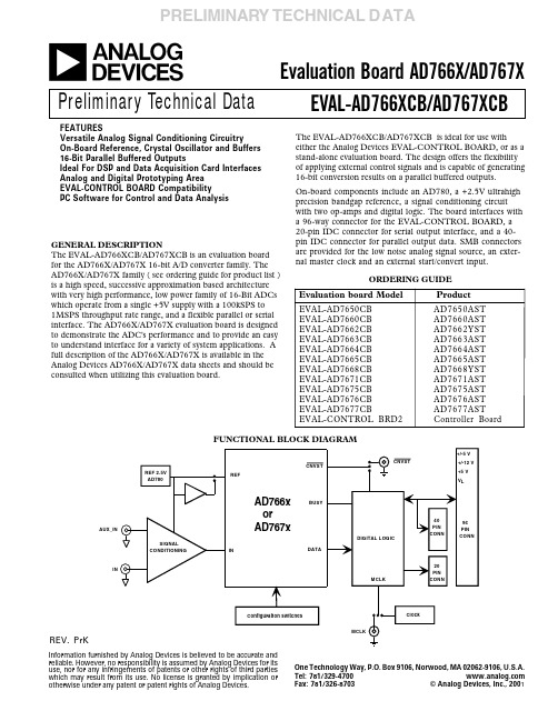
EVAL-AD7650CB中文资料
REV. PrKInformation furnished by Analog Devices is believed to be accurate and reliable. However, no responsibility is assumed by Analog Devices for its use, nor for any infringements of patents or other rights of third parties which may result from its use. No license is granted by implication or otherwise under any patent or patent rights of Analog Devices.=EV AL-AD766XCB/AD767XCBOne Technology Way, P.O. Box 9106, Norwood, MA 02062-9106, U.S.A.Tel: 781/329-4700 Fax: 781/326-8703 © Analog Devices, Inc., 2001Preliminary Technical DataPRELIMINAR Y TECHNICAL DATAEvaluation Board AD766X/AD767X FEATURESVersatile Analog Signal Conditioning CircuitryOn-Board Reference, Crystal Oscillator and Buffers 16-Bit Parallel Buffered OutputsIdeal For DSP and Data Acquisition Card Interfaces Analog and Digital Prototyping Area EVAL-CONTROL BOARD CompatibilityPC Software for Control and Data AnalysisGENERAL DESCRIPTIONThe EVAL-AD766XCB/AD767XCB is an evaluation board for the AD766X/AD767X 16-bit A/D converter family. The AD766X/AD767X family ( see ordering guide for product list )is a high speed, successive approximation based architecture with very high performance, low power family of 16-Bit ADCs which operate from a single +5V supply with a 100kSPS to 1MSPS throughput rate range, and a flexible parallel or serial interface. The AD766X/AD767X evaluation board is designed to demonstrate the ADC's performance and to provide an easy to understand interface for a variety of system applications. A full description of the AD766X/AD767X is available in the Analog Devices AD766X/AD767X data sheets and should be consulted when utilizing this evaluation board.FUNCTIONAL BLOCK DIAGRAMThe EVAL-AD766XCB/AD767XCB is ideal for use witheither the Analog Devices EVAL-CONTROL BOARD, or as a stand-alone evaluation board. The design offers the flexibility of applying external control signals and is capable of generating 16-bit conversion results on a parallel buffered outputs.On-board components include an AD780, a +2.5V ultrahigh precision bandgap reference, a signal conditioning circuit with two op-amps and digital logic. The board interfaces with a 96-way connector for the EVAL-CONTROL BOARD, a 20-pin IDC connector for serial output interface, and a 40-pin IDC connector for parallel output data. SMB connectors are provided for the low noise analog signal source, an exter-nal master clock and an external start/convert input.ORDERING GUIDEEvaluation board Model Product EVAL-AD7650CB AD7650AST EVAL-AD7660CB AD7660AST EVAL-AD7662CB AD7662YST EVAL-AD7663CB AD7663AST EVAL-AD7664CB AD7664AST EVAL-AD7665CB AD7665AST EVAL-AD7668CB AD7668YST EVAL-AD7671CB AD7671AST EVAL-AD7675CB AD7675AST EVAL-AD7676CB AD7676AST EVAL-AD7677CBAD7677AST EVAL-CONTROL BRD2Controller Board元器件交易网REV. PrK EVAL-AD766XCB/AD767XCB–2–PRELIMINARY TECHNICAL DAT AO PERATING THE EVAL-AD766XCB/AD767XCBThe EVAL-AD766XCB/AD767XCB is a four-layer board carefully laid out and tested to demonstrate the specific high accuracy performance of the AD766X/AD767X. Figure 1shows the schematics of the evaluation board. The layouts of the board are given in :Top side silk-screen - Figure 2Top side layer - Figure 3Ground layer - Figure 4Shield layer - Figure 5Bottom side layer - Figure 6Bottom side silk-screen - Figure 7.The EVAL-AD766XCB/AD767XCB is a flexible design that enables the user to choose among many different board con-figurations. A description of each selectable jumper/switch is listed in Table II and the available test points are listed in Table III. Note that the button of a switch in position A ( U3side ) defines a low level.The EVAL-AD766XCB/AD767XCB is configured in factory with 0 to 2.5 V ADC input range for the AD7660, AD7664,and AD7675/7676/7677 and +/-5V for the AD7663/7665/7671; front-end amplifiers U6 and U7 set with a gain of +1,powered through the EVAL-CONTROL BOARD, and the on-board CNVST generation used.On-board or external CNVST could be used. When an exter-nal CNVST signal is applied, this signal should have very low jitter and sharp edges to get the best noise performance of the part. Meanwhile, it is recommended to use the on-board CNVST generation which is done by dividing MCLK signal (20MHZ) by the numbers shown in Table I, which are en-tered in the software. Activity on BUSY pin of the ADC turns on the LED.Table I. CNVST GENERATIO NPart Division Factor Throughput Rate AD7660200100KSPS AD7662/6840500KSPS AD766380250KSPS AD7664/5035571KSPS AD766535571KSPS AD7671201MSPS AD7675200100KSPS AD767635571KSPS AD7677201MSPSConversion data is available at the output bus BD on U3, onthe 40-pin connector P2, and on the 96-pin connector P3.Additionally, BD data is updated on the falling/rising edge of DBUSY and BBUSY on P3, low when BD data is valid are delayed from the BD data by about 20 ns to ease the inter-face. When either parallel or serial reading mode of the ADC is used, the data is available on this parallel bus. When serial reading mode of the ADC is used, the serial interface signals of the ADC are buffered and available on the 20-pin connec-tor P1. When slave serial reading mode of theAD766X/AD767X is used, the external serial clock SCLK applied to the ADC is at half the MCLK frequency.Power Supplies and GroundingThe evaluation board ground plane is separated into twosections: a plane for the digital interface circuitry and an ana-log plane for the analog input and external referencecircuitry. To attain high resolution performance, the board was designed to ensure that all digital ground return paths do not cross the analog ground return paths.The EVAL-AD766XCB/AD767XCB has three power supply blocks: a single 5V supply VA (SJ1) for the AD766X/AD767X and the reference voltage circuitry, a digital 5V supply VL (SJ2)for the digital interface circuitry and the digital section of the ADC, and a selectable +/-12V (with a possibility of +/-15V with control Brd2) or +/-5V supply for the analog signal con-ditioning circuitry (SJ3). All supplies are decoupled to ground with 10 F tantalum and 0.1 F ceramic capacitors.Analog Input RangesThe analog front-end amplifier circuitry U6 and U7 allows flexible configuration changes such as positive or negative gain, input range scaling, filtering, addition of a DC compo-nent, use of different op-amp and supplies.Figure 1 shows the front end op-amp configuration used with the AD7660/7663/7664/7665/7671/7675/7676/7677.In some applications, it is desired to use a bipolar or wider analog input range like, for instance, ± 10V, ± 5V, ± 2.5V, or 0 to +5V. For the AD76XX parts which do not have directly those input ranges like the AD7660/7664/7675/7676/7677,by simple modifications of the input driver circuitry of the EVAL-AD766XCB/AD767XCB, bipolar and wider input ranges can be used without any performance ponents values required and resulting full-scale ranges are shown in table IV and table V.In factory, the analog input of U6 is set at mid-scale(R6=R7=590⍀) for the AD7660/7664/7675/7676/7677. For AD7663/7665/7671, R7 is not connected to maintain the input at 0V (mid-scale). This allows a transition noise test without any other equipment. An FFT test can be done by applying a very low distortion AC source.EVAL-CONTROL BOARD INTERFACEThe EVAL-AD766XCB/AD767XCB interfaces to the EVAL-CONTROL BRD2 through the 96-way connector.RUNNING THE EVAL-AD766X/AD767XCB SO FTWARE Software DescriptionThe EVAL-AD766XCB/AD767XCB comes with software for analyzing the AD766X/AD767X. Through the EVAL-CON-TROL BRD2 one can perform a histogram to determine code transition noise, and Fast Fourier Transforms (FFT's) to determine the Signal-to-Noise Ratio (SNR), Signal-to-Noise-plus-Distortion (SNRD) and Total-Harmonic-Distortion (THD). The front-end PC software has four screens asshown in Figure 8,9,10 and 11. Figure 8 is the Setup Screen where input voltage range, sample rate, number of samples are selected. Figure 9 is the Histogram Screen, which allows the code distribution for DC input and computes the meanand standard deviation.元器件交易网REV PrK –3–EVAL-AD766XCB/AD767XCBPRELIMINARY TECHNICAL DAT ATABLE II. JUMPER DESCRIPTIONJumper Default position FunctionDesignation with the controlboard ( Factory settings)Figure 10 is the FFT Screen, which performs an FFT on thecaptured data, computes the Signal-to-Noise Ratio (SNR),Signal-to-Noise-plus-Distortion (SINAD) and total-Har-monic-Distortion (THD). Figure 11 is the time domain representation of the output. When the on-board CNVST generation is used, a synchronous FFT could be achieved by synchronizing the external AC generator with the Fsync signal (TP11) which is an exact division by 2 of MCLK.Software Installation- Double-Click on Setup.exe from the CD-ROM and follow the installation instructions.NOTE: The software runs under Windows 95/98 only.JP1ASelection of the positive supply of the front-end amplifier U6. When JP1 is in posi-tion A, the +12V supply from the control board is applied to JP3 otherwise VS+ on SJ3 is used.JP2ASelection of the negative supply of the front-end amplifier U6. When JP2 is in posi-tion A, the -12V supply from the control board is applied to JP4 otherwise VS- on SJ3 is used.JP3A Selection of the positive supply of the front-end amplifier U6. When JP3 is in posi-tion A, the +5V supply from the control board is used otherwise JP1 output is used.JP4A Selection of the negative supply of the front-end amplifier U6. When JP4 is in posi-tion A, the -5V supply from the control board is used otherwise JP2 output is used.JP5not ASelection of the master clock MCLK signal. When JP5 is in position A, the signal on J4 is used otherwise the on-board 20 MHz clock is used as a MCLK signal. MCLK signal is used to generate the on-board CNVST signal and the external serial clock SCLK.JP6A, U3 sideSelection of RDC ( Read during convert ). When the button of the switch is close to J4 connector ( not A position ) and when the serial reading mode is selected, the data are read during conversion otherwise the data are read after conversion. JP6 has no use in parallel reading mode.JP7A, U3 side Selection of PD ( Powerdown ). When the button of the switch is close to J4 connec-tor ( not A position ), the ADC is in power-down mode.JP8A, U3 side Spare switch.JP9A, U3 side Selection of RESET. When the button of the switch is close to J4 connector ( not A position ), the ADC is reset.JP10A, U3 sideSelection of SER/PAR ( serial/parallel reading mode ). When the button of the switch is close to J4 connector ( not A position ), the data are read in serial mode otherwise the data are read in parallel mode.JP11not A, SJ4 sideSelection of OC/2C ( coding ). When the button of the switch is close to J4 connector ( not A position ), the ADC uses a straight binary coding otherwise the twos comple-ment coding is used.JP12A, U3 sideSelection of WARP. When the button of the switch is close to J4 connector ( not A position ), the ADC uses the WARP mode which is the fastest one. With the AD7660,JP12 is a spare switch.元器件交易网REV. PrKEVAL-AD766XCB/AD767XCB–4–PRELIMINARY TECHNICAL DAT ATable III. EVAL-AD766XCB/AD767XCB Test Points Test PointAvailable SignalTP1DGND Digital ground TP2DGND Digital ground TP3SIG+ADC Analog inputTP4AGND Analog ground close to SIG+TP5REF ADC Reference input TP6BUSY ADC BUSY signal TP7R D ADC RD signal TP8C S ADC CS signalTP9AGND Analog ground close to REF TP10CNVST ADC CNVST signal TP11F SYNC MCLK divided by 2TP12OVDD ADC digital output supply TP13DVDD ADC digital core supply TP14VANA1ADC analog supplyTP15AGND Analog ground close to SIG-TP16SIG-ADC Analog inputTable IV. Component values Vs. Input ranges ( AD7660 )Input range R1R3R6R7± 10V 8k ⍀ 1k ⍀8k ⍀10k ⍀± 5V 8k ⍀ 2k ⍀ 6.67k ⍀10k ⍀ 0 to -5V8k ⍀ 8k ⍀0⍀noneTable V. Component values Vs. Input ranges ( AD7664 )Input range R1R3R6R7± 10V2k ⍀ 250⍀8k ⍀10k ⍀± 5V 2k ⍀ 500⍀ 6.67k ⍀10k ⍀ 0 to -5V1k ⍀ 1k ⍀0⍀noneJumper Default positionFunctionDesignation with the controlboard ( Factory settings)TABLE II. JUMPER DESCRIPTIO NJP13A, U3 sideSelection of IMPULSE. When the button of the switch is close to J4 connector ( not A position ), the ADC uses the IMPULSE mode which is the mode with the lowest power dissipation. With the AD7660, JP13 is a spare switch.JP14A, U3 side TEST1. For factory use only and it is pull down.JP15A, U3 side TEST0. For factory use only and it is pull down.JP16A, U3 sideSelection of EXT/INT ( use of external or internal serial clock ). When the button of the switch is close to J4 connector ( not A position ) and when the serial readingmode is selected, the data are read with an external serial clock SCLK generated from the master clock MCLK otherwise the data are read with the ADC serial clock. When external serial clock reading mode is selected, MCLK has to be fast enough to be able the read the data properly as explained in the AD766X data sheet. JP16 has no use in parallel reading mode.JP17A, U3 sideSelection of INVSYNC ( SYNC active level ). When the button of the switch is close to J4 connector ( not A position ) and when the master serial reading mode is se lected, the SYNC signal is active Low. JP17 has no use in parallel reading mode or slave serial reading mode.JP18A, U3 sideSelection of INVSCLK ( SCLK active edge ). When the button of the switch is close to J4 connector ( not A position ) and when the serial reading mode is selected,INVSCLK is high. JP18 has no use in parallel reading mode.JP19not ASelection of CNVST signal. When JP19 is in position A, the signal on J3 is usedotherwise the on-board CNVST generation is used. MCLK signal is used to generate the on-board CNVST signal.J P20not ASelection of REF signal. When J P20 is in position A, the REF is buffered. When J P20 is not in position A, the REF is not buffered.元器件交易网EVAL-AD766XCB/AD767XCB PRELIMINARY TECHNICAL DAT ATESTING METHO DSHistogramTo perform a histogram test, apply a DC signal to the input. It is advised to filter the signal to make the DC Source noise com-patible with that of the ADC. C26 provides this filtering.AC TestingTo perform an AC test, apply a sinusoidal signal to the evaluation board. Low distortion, better than 100dB, is required to allow true evaluation of the part. One possibility is to filter the input signal from the AC source. There is no suggested bandpass filter but consideration should be taken in the choice. Furthermore, when the full-scale input range is more than a few Vpp, it is recommended that you use the on board amplifier to amplify the signal, thus preventing the filter from distorting the input signal.Please refer to Figures 8,9,10 and 11 to see the screens of the software.Software DescriptionThe AD16bit.exe is the software which allows you to analyze different performance characteristics of the AD766X,AD767X, AD97X and AD67X 16-bit ADC family. The soft-ware allows you to test the histogram as well as perform different AC tests.Setup Requirements- Evaluation Control Board 2 (ADSP2189)- Evaluation Board- Power Supply (AC 15V/1A source could be bought from ADI)- Parallel Port Cable (provided with the evaluation control board)- AC Source (low distortion)- DC Source (low noise)- Bandpass Filter (value based on your signal frequency, low distortion)USE O F EVAL-AD766XCB/AD767XCB AS STAND-ALO NE EVALUATIO N BO ARDYou have the option of using theEVAL-AD766XCB/AD767XCB as a stand-alone evaluation board. This method does not require the control board, nor does it require use of the accompanied software. The digital output will now be available on P1 (20-pin connector, for use in serial mode) or P2 (40-pin connector, for use in parallel mode). Cer-tain modifications have to be made on the board to allow proper operation of the evaluation board. Refer to Table II to obtain the jumper positions for stand-alone operation. When in stand-alone, CNVST could be externally applied or is generated internally according to Table I.Please refer to Figure 1 to obtain the data output pins on the connectors.Data is updated on the falling edge of BUSY. BCS and BWRare inputs to the FPGA and are connected to P1 and P2.When BCS, CONTROL are low and BWR is high, which isthe default value defined by the on-board pull-up/pull-down resistors, the data bus BD available on the P2 connector is enabled.SUPPLYING THE BO ARD FO R STAND-ALO NE USESJ1 is the analog supply. Connect VA+ to +5V and AGND to GND. SJ2 is the digital supply. SJ2 requires the same values as SJ1, and SJ2 may be connected to SJ1. SJ3 is the supply for the front end amplifier (U6). Connect +12V to VS+, GND to AGND, and -12V to VS-.元器件交易网REV PrK –5–REV PrKEVAL-AD766XCB/AD767XCB–6–PRELIMINARY TECHNICAL DAT AEVAL-BO ARD SETTING FO R INPUT CONFIGURATIONSThe AD7663/AD7665 and AD7671 have the ability to oper-ate both unipolar and bipolar range. The available options are +/- 10V, +/- 5V, +/- 2.5V, 0 to 10V, 0 to 5V and 0 to 2.5V.Table VI shows the required configurations for each input range. (REF = 2.5V). Table VII lists the default settings of the board for all parts.Table VI.AD7663/7665/7671 Analog Input ConfigurationInput Voltage IND(4R)INC(4R)INB(2R)INA(R) Range ±4 REF V IN INGND INGND REF ±2 REF V IN V IN INGND REF ±REFV IN V IN V INREF 0 V to 4REF V IN V IN INGND INGND 0 V to 2REF V IN V IN V IN INGND 0 V to REFV INV INV INV INTable VII. Default SettingsComponent/PartR7S9S10R48C40R47C39AD7660590⍀None 0⍀0⍀None AD7663None None 0⍀0⍀None AD7664590⍀None 0⍀15⍀ 2.7nF AD7665None None 0⍀0⍀None AD7671None None 0⍀0⍀None AD7675590⍀0⍀None 15⍀ 2.7nF 15⍀ 2.7nF AD7676590⍀0⍀None 15⍀ 2.7nF 15⍀ 2.7nF AD7677590⍀0⍀None15⍀2.7nF15⍀2.7nF元器件交易网PRELIMINARY TECHNICAL DAT A元器件交易网EVAL-AD766XCB/AD767XCBREV PrK –7–REV. PrKEVAL-AD766XCB/AD767XCB–8–PRELIMINARY TECHNICAL DAT AFigure 1Schematic元器件交易网REVEVAL-AD766XCB/AD767XCBPRELIMINARY TECHNICAL DAT A元器件交易网REV. PrKEVAL-AD766XCB/AD767XCBPRELIMINARY TECHNICAL DAT A元器件交易网Figure 8.Setup Screen2) The part under evaluation is chosen from this menu. Theavailable choices are AD766X, AD97x and AD67x.5) You may choose to take one sample (Sample,F3), or per-form continuous sampling (Continuous,F4). You may also choose the Help, Save, Print or Quit options. The Help menu will show you a description of the functionality of the chosen command.4) The choice of test is made here. You may choose to perform either a Histogram test or an AC test.1) The Run button starts the software. All input configurations are read by the software after running the software. You will need to press this button first.3) Input Configurations are chosen here. For the AD766X/AD767X, the available choices are: PwDown, Reset, Interface,Coding, Byte, and Reading.This is the performance window.Figure 9.Histogram ScreenDifferent measurements are displayed here. The DC value,transition noise, and other values.This control allows you the choice of display. You have the option of Time or Histogram. You also have the option of changing the X-axis unitThe results are displayed on this chart. You may also use thecursor (yellow) and drag it to your desired location, where the X-axis value and the Y-axis value will be displayed.Figure 10.FFT ScreenAC test results are shown here. You also have the choice of viewing the amplitude of a certain FFT component by changing the FFT component menu .You may choose either a Kaiser window or a Blackmann-Har-ris window or a Sync FFT from this menu. . When choosing a Sync FFT, you will need to synchronize your analog source to the sampling frequency. The input frequency should be the value Sync Fr, which is to the right of Target frequency. The process for this is as follows:1. You Choose a Target frequency2. The software calculates an integer n based on the target frequency you entered and the sampling frequency, Fsamp.3. The software rounds up the value n to the next prime number.4. The software then calculates the corresponding input fre-quency (Fin) and displays that as Sync Fr.The equation, (capture window size) is shown below:(1/Fsamp) * (number of samples) = n * (1/Fin)This is the control that allows you the choice of either time domain or frequency domain. You may also change the X-axis unit here.The results are displayed on this chart. You may also use thecursor (yellow) and drag it to your desired location, where the X-axis value and the Y-axis value will be displayed.You can also view the output in the Time domain as shown below.Figure 11.Time-Domain ScreenTo view the Time domain, select Time in this menu.。
运算放大器ICL7650工作原理

运放ICL7650中文资料ICL7650是Intersil公司利用动态校零技术和CMOS工艺制作的斩波稳零式高精度运算放大器,它具有输入偏置电流小、失调小、增益高、共模抑制能力强、响应快、漂移低、性能稳定及价格低廉等优点。
图1 ICL7650 引脚图ICL7650采用14脚双列直插式和8脚金属壳两种封装形式,图1所示是最常用的14脚双列直插式封装的引脚排列图。
各引脚功能说明如下:CEXTB:外接电容CEXTB;CEXTA:外接电容CEXTA;-IN:反相输入端;+IN:同相输入端;V-:负电源端;CRETN:CEXTA和CEXTB的公共端;CLAMP:箝位端;OUTPUT:输出端;V+:正电源端;INTCLKOUT:时钟输出端;EXTCLKIN:时钟输入端;时钟控制端,可通过该端选择使用内部时钟或外部时钟。
当选择外部时钟时,该端接负电源端(V-),并在时钟输入端(EXTCLKIN)引入外部时钟信号。
当该端开路或接V+时,电路将使用内部时钟去控制其它电路的工作。
ICL7650工作原理ICL7650利用动态校零技术消除了CMOS器件固有的失调和漂移,从而摆脱了传统斩波稳零电路的束缚,克服了传统斩波稳零放大器的这些缺点。
ICL7650的工作原理如图2所示。
图中,MAIN是主放大器(CMOS运算放大器),NULL是调零放大器(CMOS高增益运算放大器)。
电路通过电子开关的转换来进行两个阶段工作,第一是在内部时钟(OSC)的上半周期,电子开关A和B导通,和C断开,电路处于误差检测和寄存阶段;第二是在内部时钟的下半周期,电子开关和C导通,A和B断开,电路处于动态校零和放大阶段。
由于ICL7650中的NULL运算放大器的增益A0N一般设计在100dB左右,因此,即使主运放MAIN的失调电压VOSN达到100mV,整个电路的失调电压也仅为1μV。
由于以上两个阶段不断交替进行,电容CN和CM将各自所寄存的上一阶段结果送入运放MAIN、NULL的调零端,这使得图2所示电路几乎不存在失调和漂移,可见,ICL7650是一种高增益、高共模抑制比和具有双端输入功能的运算放大器。
基于 ICL7650的温湿度传感器设计

基于 ICL7650的温湿度传感器设计孙佳;漆随平;王东明【摘要】介绍了斩波稳零式高精度运算放大器ICL7650的工作原理、性能以及在温湿度传感器设计中的应用。
采用ICL7650作为前置电路的运算放大器,辅以低功耗的外围扩展元器件,设计了具有两路4~20 mA模拟电流输出的温湿度传感器。
试验证明,基于ICL7650所设计的温湿度传感器具有低功耗、高精度及稳定性好等优点。
%This paper introduces the work principle and main capability of ICL7650 ,and applications in temperature‐humidity sensor .Uses ICL7650 as the main amplifier ,including some other chips ,realizes the temperature‐humidity sensor which has two outputs of 4~20 mA analog current signals .According to the examination ,the te mperature‐humidity sensor through ICL7650 possesses some excellences ,such as lowpower ,high precision and good stability .【期刊名称】《机械管理开发》【年(卷),期】2015(000)001【总页数】3页(P6-7,66)【关键词】ICL7650;温湿度传感器;运算放大器【作者】孙佳;漆随平;王东明【作者单位】山东省海洋环境监测技术重点实验室,山东青岛 266001; 山东省科学院海洋仪器仪表研究所,山东青岛 266001; 国家海洋监测设备工程技术研究中心,山东青岛 266001;山东省海洋环境监测技术重点实验室,山东青岛 266001;山东省科学院海洋仪器仪表研究所,山东青岛 266001; 国家海洋监测设备工程技术研究中心,山东青岛 266001;山东省海洋环境监测技术重点实验室,山东青岛266001; 山东省科学院海洋仪器仪表研究所,山东青岛 266001; 国家海洋监测设备工程技术研究中心,山东青岛 266001【正文语种】中文【中图分类】TH715.2引言大气环境的温度和相对湿度是船舶气象仪气象观测要素中非常重要的气象要素[1]。
裸芯片种类
LF351LF353LF356LF357LF411LF412LF441ALF442LF444LM107
LM108LM108ALM118LM12LM124LM143LM1458LM148LM1556LM158
缓冲放大器
HA0-5002HA0-5033HA-5002HAO-5033
测量放大器
AD524AD620AD622AD623AD624AD625AD627AMP02FSINA110INA111
INA118INA122INA128INA128AINA129NA129AINA163INA2321INA321LTC6800
TMS29F040X76F100
随机存取存储器(RAM)
IDT6116SAUIDT7026IDT7164IS61LV12816LIS61LV5128ALK4H561638DK6R4008CIDK6R4016V1DMK68345MT28C6428P18
LT1057CLT1494LT1495LT1803LT1880LT6233LTC1052MA01MAX4020MAX407
MAX4385EMAX4472MAX492MAX495MC1456MC1536MC1537MC1556MC3303MC33171
MC3503MC4741MCC1536MSK103NE5532OP07GBCOP07GRBCOP07NBCOP09OP11GBC
可变增益放大器
AD603AAD604SAD8367AD8369THS7530VCA810
视频放大器
AD813LM733LT1227TL592UA733C
ICL7650ITV资料

120
AVOL
Large-Signal Voltage Gain
RL = 10k, VOUT = ±4V
● 120 150
120
VOUT
Maximum Output Voltage Swing RL = 10k
(Note 4)
RL = 100k
● ±4.7 ±4.85
±4.7
±4.95
SR
Slew Rate
TOP VIEW
CEXTA 1
– IN 2 – +N 3 +
V– 4
8 CEXTB
7 V+
6 OUTPUT
5
OUTPUT CLAMP
N8 PACKAGE 8-LEAD PDIP
TJMAX = 110°C, θJA = 150°C/W
J8 PACKAGE, 8-LEAD CERDIP
OBSOLETE PACKAGE
UW U PACKAGE/ORDER I FOR ATIO
CEXTA 1
TOP VIEW CEXTB
8 7 V+/CASE
–
– IN 2
+
6 OUTPUT
+ IN 3
5 LTC1052 OUTPUT CLAMP
4
LTC7652 CRETURN
ICL7650斩波稳零运算放大器的原理及应用

-41-IC L7650斩波稳零运算放大器的原理及应用解放军电子工程学院吴祖国Princi p le and A pp lications of ICL7650Cho pp er -StabilizedO p erational Am p lifierWu Zu g uo摘要:介绍了Intersil 公司生产的斩波稳零式高精度运算放大器IC L7650的结构及性能,分析了动态校零的基本工作原理,给出了IC L7650在地震前兆信号采集系统中的应用实例。
关键词:斩波稳零;运算放大器;IC L7650分类号:T N722文献标识码:B 文章编号:1006-6977(2003)04-0041-03●新特器件应用IC L7650斩波稳零运算放大器的原理及应用IC L7650是Intersil 公司利用动态校零技术和CM OS 工艺制作的斩波稳零式高精度运放,它具有输入偏置电流小、失调小、增益高、共模抑制能力强、响应快、漂移低、性能稳定及价格低廉等优点。
1芯片结构IC L7650采用14脚双列直插式和8脚金属壳两种封装形式,图1所示是最常用的14脚双列直插式封装的引脚排列图。
各引脚的功能说明如下:C EXT B :外接电容C EXT B ;C EXT A :外接电容C EXT A ;-IN:反相输入端;+IN:同相输入端;V -:负电源端;C RET N :C EXT A 和C EXT B 的公共端;OUT C LAMP:箝位端;●欠压锁定输出极限电压:12V;●欠压锁定输出延迟电压:2.9V 。
4240W/12V 直流开关电源电路图3所示是由FAN4803组成的一个12V/240W直流开关电源的实用电路。
其中FAN4803的电源电压VCC 由R26、R27、R31、CR9、R21组成的分压稳压电路和C6、C27、C28组成的旁路滤波电路来提供,该网络中的稳压管CR9可为FAN4803提供17.5V 的稳定电压。
ICL7650CSA+中文资料

ICL7650 ICL7653
R
C
OUTPUT C
INVERTING AMPLIFIER WITH OPTIONAL CLAMP
Features
o ICL7650/53 are Improved Second Sources to ICL7650B/53B
o Lower Supply Current: 2mA o Low Offset Voltage: 1µV o No Offset Voltage Trimming Needed o High-Gain CMRR and PSRR: 120dB min o Lower Offset Drift with Time and Temperature o Extended Common-Mode Voltage Range o Low DC Input Bias Current: 10pA o Monolithic, Low-Power CMOS Design
The ICL7650B/ICL7653B are exact replacements for Intersil’s ICL7650B/ICL7653B. These devices have a 10µV max offset voltage, a 0.1µV/°C max input offset voltage temperature coefficient, and a 20pA max bias current—all specified over the commercial temperature range.
8-Pin SO (derate 5.88mW/°C above +70°C)...............471mW 8-Pin PDIP (derate 6.9mW/°C above +70°C)...............552mW 8-Pin CERDIP (derate 8.0mW/°C above +70°C).........640mW
ICL8052ACDD资料

Features•Typically Less Than 2µV P-P Noise (200.00mV Full Scale, lCL8068)•Accuracy Guaranteed to±1 Count Over Entire±20,000 Counts (2.0000V Full Scale)•Guaranteed Zero Reading for 0V Input•True Polarity at Zero Count for Precise Null Detection •Single Reference Voltage Required•Over-Range and Under-Range Signals Available for Auto-Ranging Capability•All Outputs TTL Compatible•Medium Quality Reference, 40ppm (Typ) on Board •Blinking Display Gives Visual Indication of Over Range•Six Auxiliary Inputs/Outputs are Available for Interfacing to UARTs, Microprocessors or Other Complex Circuitry•5pA Input Current (Typ) (8052A)DescriptionThe ICL8052 or ICL8068/lCL71C03 chip pairs with their multiplexed BCD output and digit drivers are ideally suited for the visual display DVM/DPM market. The outstanding 41/2 digit accuracy, 200.00mV to 2.0000V full scale capabil-ity, auto-zero and auto-polarity combine with true ratiometric operation, almost ideal differential linearity and time-proven dual slope conversion. Use of these chip pairs eliminates clock feedthrough problems, and avoids the critical board layout usually required to minimize charge injection.When only 2000 counts of resolution are required, the 71C03 can be wired for 31/2 digits and give up to 30 readings/sec., making it ideally suited for a wide variety of applications.The ICL71C03 is an improved CMOS plug-in replacement for the lCL7103 and should be used in all new designs.PinoutsOrdering InformationPART NUMBERTEMP.RANGE (o C)PACKAGEPKG.NO.ICL8052CPD0 to 7014 Ld PDIP E14.3lCL8052CDD0 to 7014 Ld CERDIP F14.3lCL8052ACPD0 to 7014 Ld PDIP E14.3ICL8052ACDD0 to 7014 Ld CERDIP F14.3ICL8068CDD0 to 7014 Ld CERDIP F14.3ICL8068ACDD0 to 7014 Ld CERDIP F14.3lCL8068ACJD0 to 7014 Ld CERDIP F14.3ICL71C03CPl0 to 7028 Ld PDIP E28.6lCL71C03ACPl0 to 7028 Ld PDIP E28.6ICL8052/ICL8068(CERDIP, PDIP)TOP VIEWICL71C03 (PDIP)TOP VIEWV-COMP OUTREF CAPREF BYPASSGNDREF OUT REF SUPPL YINT OUT+BUFF IN+INT IN-INT IN-BUFF INBUFF OUTV++1234567141312111098-1.2VV REFICL8052/ICL8068V+41/2/ 31/2POLRUN/HOLDCOMP INV-REFERENCEREF. CAP. 1REF. CAP. 2ANALOG INANALOG GNDCLOCK INUNDER-RANGEOVER-RANGEBUSYD2D3D4B8 (MSB)B2D5 (MSD)STROBEA-Z INA-Z OUTDIGITAL GNDD1 (LSD)B4B1 (LSB)28272625242322212019181716151234567891011121314August 1997ICL8052/ICL71C03, ICL8068/ICL71C03 Precision 41/2 Digit, A/D ConverterFile Number3081.1CAUTION: These devices are sensitive to electrostatic discharge; follow proper IC Handling Procedures.元器件交易网Functional Block DiagramFIGURE 1.A2+-A3+-INTEG.COMP.A1+-BUFFER14119INT OUT-INT IN BUF OUT 10-BUF IN-1.2V21-15V78+15V 12+INT IN 13ICL8052/8068INT.REF.63+BUF IN 5REF OUT10k Ω1k Ω300pF10µFCOMPOUTCOMP IN5169MULTIPLEXERCOUNTERS20CONTROL LOGICZERO CROSSING DETECTOR212223ICL71C03REF AZ OUTSW31+5V ANALOG GNDANALOG INPUT28BUSY 18STROBE 13UNDER 1412CLOCK 24 1/2 DIGIT/2651410µF (TYP)CAP 2REF CAP 187101110k Ω0.1µF REF1µF (TYP)17AZ IN 6-15V150.22µF10k Ω90k Ω100k Ω4IN RUN/HOLDRANGEOVER RANGE 3 1/2 DIGIT B 1B 2B 3B 4LATCHLATCH LATCH LATCHLATCHLSDMSDSEVEN-SEGMENT DECODER3P O L A R I T Y1924252627D 5D 4D 3D 2D 1Absolute Maximum Ratings Thermal InformationICL8052, ICL8068Supply Voltage . . . . . . . . . . . . . . . . . . . . . . . . . . . . . . . . . . . . .±18V Differential Input Voltage(8068) . . . . . . . . . . . . . . . . . . . . . . . . . . . . . . . . . . . . . . . . . .±30V (8052) . . . . . . . . . . . . . . . . . . . . . . . . . . . . . . . . . . . . . . . . . . .±6V Input Voltage (Note 1). . . . . . . . . . . . . . . . . . . . . . . . . . . . . . . .±15V Output Short Circuit Duration All Outputs (Note 2). . . . . . .Indefinite ICL71C03Power Supply Voltage (GND to V+) . . . . . . . . . . . . . . . . . . . . . 6.5V Negative Supply Voltage (GND to V-). . . . . . . . . . . . . . . . . . . . .-17V Analog Input Voltage (Note 3) . . . . . . . . . . . . . . . . . . . . . . .V+ to V-Digital Input Voltage (Note 4) . . . . . . . .(GND - 0.3V) to (V+ + 0.3V) Operating ConditionsTemperature Range . . . . . . . . . . . . . . . . . . . . . . . . . . . .0o C to 70o C Thermal Resistance (T ypical, Note 5)θJA (o C/W)θJC (o C/W) CERDIP Package . . . . . . . . . . . . . . . . 752014 Ld PDIP Package. . . . . . . . . . . . . .100N/A28 Ld PDIP Package. . . . . . . . . . . . . .65N/A Maximum Storage Temperature . . . . . . . . . . . . . . . .-65o C to 150o C Maximum Lead T emperature (Soldering, 10s) . . . . . . . . . . . .300o CCAUTION: Stresses above those listed in “Absolute Maximum Ratings” may cause permanent damage to the device. This is a stress only rating and operation of the device at these or any other conditions above those indicated in the operational sections of this specification is not implied.NOTES:1.For supply voltages less than±15V, the absolute maximum input voltage is equal to the supply voltage.2.Short circuit may be to ground or either supply. Rating applies to 70o C ambient temperature.3.Input voltages may exceed the supply voltages provided the input current is limited to±100µA.4.Connecting any digital inputs or outputs to voltages greater then V+ or less than GND may cause destructive device latchup. For thisreason it is recommended that the power supply to the ICL71C03 be established before any inputs from sources not on that supply are applied.5.θJA is measured with the component mounted on an evaluation PC board in free air.Electrical SpecificationsPARAMETER SYMBOLTESTCONDITIONS MIN TYP MAX UNITSClock In, Run/Hold, 4 1/2 /3 1/2I INL V IN = 0-0.20.6mAI INH V IN = +5V-0.110µA Comp. In Current I INL V IN = 0-0.110µAI INH V IN = +5V-0.110µA Threshold Voltage V INTH- 2.5-VAll Outputs V OL I OL = 1.6mA-0.250.40VB1, B2, B4, B8,D1, D2, D3, D4, D5V OH I OH = -1mA 2.4 4.2-V Busy,Strobe, Over-Range, Under-Range Polarity V OH I OH = -10µA 4.9 4.99-V Switches 1, 3, 4, 5, 6r DS(ON)-400-ΩSwitch 2r DS(ON)-1200-ΩSwitch Leakage (All)I D(OFF)-2-pA+5V Supply Range V+456V-15V Supply Range V--5-15-18V+5V Supply Current I+f CLK = 0- 1.13mA-15V Supply Current I-f CLK = 0-0.83mA Power Dissipation Capacitance C PD vs Clock Frequency-40-pF Clock Frequency (Note 6)DC20001200kHz NOTE:6.This specification relates to the clock frequency range over which the ICL71C03(A) will correctly perform its various functions. See the“Max Clock Frequency” section under Component Value Selection for limitations on the clock frequency range in a system.ICL8068 Electrical Specifications V SUPPL Y =±15V, T A = 25o C, Unless Otherwise SpecifiedPARAMETER SYMBOLTESTCONDITIONSICL8068ICL8068AUNITS MIN TYP MAX MIN TYP MAXEACH OPERATIONAL AMPLIFIERInput Offset Voltage V OS V CM = 0V-2065-2065mV Input Current (Either Input) (Note 7)I IN V CM = 0V-175250-80150pA Common-Mode Rejection Ratio CMRR V CM =±10V7090-7090-dB Non-Linear Component of Common-Mode Rejection Ratio (Note 8)V CM =±2V-110--110-dB Large Signal Voltage Gain A V R L = 50kΩ20,000--20,000--V/V Slew Rate SR-6--6-V/µs Unity Gain Bandwidth GBW-2--2-MHz Output Short-Circuit Current I SC-5--5-mA COMPARATOR AMPLIFIERSmall-Signal Voltage Gain A VOL R L = 30kΩ--4000---V/V Positive Output Voltage Swing+V O1213-1213-V Negative Output Voltage Swing-V O-2.0-2.6--2.0-2.6-V VOLTAGE REFERENCEOutput Voltage V O 1.5 1.75 2.0 1.60 1.75 1.90V Output Resistance R O-5--5-ΩTemperature Coefficient TC-50--40-ppm/o C Supply Voltage (V++ -V-)V SUPPL Y±10-±16±10-±16V Supply Current Total I SUPPL Y--14-814mA ICL8052 Electrical Specifications V SUPPL Y =±15V, T A = 25o C, Unless Otherwise SpecifiedPARAMETER SYMBOLTESTCONDITIONSICL8052ICL8052AUNITS MIN TYP MAX MIN TYP MAXEACH OPERATIONAL AMPLIFIERInput Offset Voltage V OS V CM = 0V-2075-2075mV Input Current (Either Input) (Note 7)I IN V CM = 0V-550-210pA Common-Mode Rejection Ratio CMRR V CM =±10V7090-7090-dB Non-Linear Component of Common-Mode Rejection Ratio (Note 8)V CM =±2V-110--110-dB Large Signal Voltage Gain A V R L = 50kΩ20,000--20,000--V/V Slew Rate SR-6--6-V/µs Unity Gain Bandwidth GBW-1--1-MHz Output Short-Circuit Current I SC-20--20-mACOMPARATOR AMPLIFIERSmall-Signal Voltage Gain A VOL R L = 30kΩ-4000----V/V Positive Output Voltage Swing+V O1213-1213-V Negative Output Voltage Swing-V O-2.0-2.6--2.0-2.6-V VOLTAGE REFERENCEOutput Voltage V O 1.5 1.75 2.0 1.60 1.75 1.90V Output Resistance R O-5--5-ΩTemperature Coefficient TC-50--40-ppm/o C Supply Voltage (V++ -V-)V SUPPL Y±10-±16±10-±16V Supply Current Total I SUPPL Y-612-614mA NOTES:7.The input bias currents are junction leakage currents which approximately double for every 10o C increase in the junction temperature,T J. Due to limited production test time, the input bias currents are measured with junctions at ambient temperature. In normal operation the junction temperature rises above the ambient temperature as a result of internal power dissipation, P D.T J=T A+RθJA P D, where RθJA is the thermal resistance from junction to ambient. A heat sink can be used to reduce temperature rise.8.This is the only component that causes error in dual-slope converter.System Electrical Specifications:ICL8068/ICL71C03V++ = +15V, V+ = +5V, V- = -15V, T A = 25o C, f CLK Set for 3 Readings/Sec.PARAMETERTESTCONDITIONSICL8068A/ICL71C03(NOTE 9)ICL8068A/ICL71C03(NOTE 10)UNITS MIN TYP MAX MIN TYP MAXZero Input Reading V IN = 0V,Full Scale = 200mV -000.0±000.0+000.0-000.0±000.0000.0DigitalReadingRatiometric Error (Note 11)V IN = V REFFull Scale = 2V 0.999 1.000 1.0010.9999 1.0000 1.0001DigitalReadingLinearity Over± Full Scale (Error ofReading from Best Straight Line)-2V≤ V IN≤ +2V-0.21-0.51CountsDifferential Linearity (Differencebetween Worst Case Step of AdjacentCounts and Ideal Step)-2V≤ V IN≤ +2V-0.01--0.01-CountsRollover Error (Difference in Readingfor Equal Positive & Negative VoltageNear Full Scale)-V IN≅ +V IN≈2V-0.21-0.51CountsNoise (P-P Value Not Exceeded 95% of Time)V IN = 0V,Full Scale = 200mV-3--2-µVLeakage Current at Input V IN = 0V-200300-100200pA Zero Reading Drift (Note 12)V IN = 0V,0o C≤ T A ≤50o C-15-0.52µV/o CScale Factor Temperature Coefficient (Note 12)V IN = 2V,0o C≤ T A ≤50o CExt. Ref. 0ppm/o C-315-25ppm/o CICL8052 Electrical Specifications V SUPPL Y =±15V, T A = 25o C, Unless Otherwise Specified (Continued)PARAMETER SYMBOLTESTCONDITIONSICL8052ICL8052AUNITS MIN TYP MAX MIN TYP MAXDetailed DescriptionANALOG SECTIONFigure 2 shows the equivalent Circuit of the Analog Section of both the ICL71C03/8052 and the ICL71C03/8068 in the 3 different phases of operation. IF the RUN/HOLD pin is left open or tied to V+, the system will perform conversions at a rate determined by the clock frequency: 40,0002 at 41/2 digit and 4002 at 31/2 digit clock periods per cycle (see Figure 3 for details of conversion timing).Auto-zero Phase I(Figure 2A)During the Auto-Zero, the input of the buffer is connected to V REF through switch 2, and switch 3 closes a loop around the integrator and comparator, the purpose of which is to charge the auto-zero capacitor until the integrator output does not change with time. Also, switches 1 and 2 recharge the reference capacitor to V REF.Input Integrate Phase II(Figure 2B)During Input Integrate the auto-zero loop is opened and the ANALOG INPUT is connected to the BUFFER INPUT through switch 4 and C REF. If the input signal is zero, the buffer, integrator and comparator will see the same voltage that existed in the previous state (Auto-Zero). Thus, the integrator output will not change but will remain stationary during the entire Input Integrate cycle. If V IN is not equal to zero, and unbalanced condition exists compared to the Auto Zero phase, and the integrator will generate a ramp whose slope is proportional to V IN. At the end of this phase, the sign of the ramp is latched into the polarity F/F. Deintegrate Phase II(Figures 2C and 2D)During the Deintegrate phase, the switch drive logic uses the output of the polarity F/F in determining whether to close switch 6 or 5. If the input signal is positive, switch 6 is closed and a voltage which is V REF more negative than during Auto-Zero is impressed on the BUFFER INPUT. Negative Inputs will cause +2(V REF) to be applied to the BUFFER INPUT via switch 5. Thus, the reference capacitor generates the equivalent of a (+) or (-) reference from the single reference voltage with negligible error. The reference voltage returns the output of the integrator to the zero-crossing point established in Phase I. The time, or number of counts, required to do this is proportional to the input voltage. Since the Deintegrate phase can be twice as long as the Input Integrate Phase, the input voltage required to give a full scale reading is 2V REF.System Electrical Specifications:ICL8052/ICL71C03V++ = +15V, V+ = +5V, V- = -15V, T A = 25o C, f CLK Set for 3 Reading/Sec.PARAMETERTESTCONDITIONSICL8068A/ICL71C03(NOTE 9)ICL8068A/ICL71C03(NOTE 10)UNITS MIN TYP MAX MIN TYP MAXZero Input Reading V IN = 0V,Full Scale = 2V -0.000±0.000+0.000-0.000±0.0000.000DigitalReadingRatiometric Error (Note 11)V IN = V REFFull Scale = 2V 0.999 1.000 1.0010.9999 1.0000 1.0001DigitalReadingLinearity Over± Full Scale (Error ofReading from Best Straight Line)-2V≤ V IN≤ +2V-0.21-0.51CountsDifferential Linearity (Differencebetween Worst Case Step of AdjacentCounts and Ideal Step)-2V≤ V IN≤ +2V-0.01--0.01-CountsRollover Error (Difference in Readingfor Equal Positive & Negative VoltageNear Full Scale)-V IN≅ +V IN≈2V-0.21-0.51CountsNoise (Peak-To-Peak Value Not Exceeded 95% of Time)V IN = 0V,Full Scale = 200mV,Full Scale = 2V-2050----30--µVLeakage Current at Input V IN = 0V-530-310pA Zero Reading Drift V IN = 0V,0o C To 70o C-15-0.52µV/o CScale Factor Temperature Coefficient V IN = 2V,0o C To 70o C,Ext. Ref. 0ppm/o C-315-25ppm/o CNOTES:9.Tested in 31/2 digit (2,000 count) circuit shown in Figure 5, clock frequency 12kHz. Pin 2 71C03 connected to GND.10.Tested in 41/2 digit (20,000 count) circuit shown in Figure 5, clock frequency 120kHz. Pin 2 71C03A open.11.Tested with a low dielectric absorption integrating capacitor. See Component Selection Section.12.The temperature range can be extended to 70o C and beyond if the Auto-Zero and Reference capacitors are increased to absorb the hightemperature leakage of the 8068.FIGURE 2A.PHASE I AUTO-ZEROFIGURE 2B.PHASE II INTEGRATE INPUTFIGURE 2C.PHASE III + DEINTEGRATEFIGURE 2D.PHASE III - DEINTEGRATEFIGURE 2.ANALOG SECTION OF EITHER ICL8052 OR ICL8068 WITH ICL71C03A2+-A3+-INTEGRATORCOMPARATORA1+-BUFFERC INT 3R INTC AZZERO CROSSING DETECTOR2651V REF (+1.000V)C REF4C STRAYV IN1µF A2+-A3+-INTEGRATORCOMPARATORA1+-BUFFERC INT 3R INTC AZZERO CROSSING DETECTOR2651V REF (+1.000V)C REF4C STRAYV IN1µF POLARITYFFA2+-A3+-INTEGRATORCOMPARATORA1+-BUFFERC INT 3R INTC AZZERO CROSSING DETECTOR2651V REF (+1.000V)C REF4C STRAYV IN1µF POLARITYFFA2+-A3+-INTEGRATORCOMPARATORA1+-BUFFERC INT 3R INTC AZZERO CROSSING DETECTOR2651V REF (+1.000V)C REF4C STRAYV IN1µF POLARITYFFZero-Crossing Flip-FlopFigure 4 shows the problem that the zero-crossing F/F is designated to solve.The integrator output is approaching the zero-crossing point where the count will be latched and the reading displayed.For a 20,000 count instrument, the ramp is changing approximately 0.50mV per clock pulse (10V Max integrator output divided by 20,000 counts). The clock pulse feedthrough superimposed upon this ramp would have to be less than 100mV peak to avoid causing significant errors.The flip-flop interrogates the data once every clock pulse after the transients of the previous clock pulse and half-clock pulse have died down. False zero-crossings caused by clock pulses are not recognized. Of course, the flip-flop delays the true zero-crossing by one count in every instance, and if a correction were not made, the display would always be one count too high. Therefore, the counter is disabled for one clock pulse at the beginning of phase 3. This one count delay compensates for the delay of the zero crossing flip-flop, and allows the correct number to be latched into the display. Similarly, a one count delay at the beginning of phase 1 gives an overload display of 0000 instead of 0001.No delay occurs during phase 2, so that true ratiometric readings result.Detailed DescriptionDIGITAL SECTIONThe 71C03 includes several pins which allow it to operate conveniently in more sophisticated systems. These include:4-1/2 /3-1/2 (Pin 2)When high (or open) the internal counter operates as a full 41/2 decade counter, with a complete measurement cycle requiring 40,002 counts. When held low, the least significant decade is cleared and the clock is fed directly into the next decade. A measurement cycle now requires only 4,0002clock pulses. All 5 digit drivers are active in either case, with each digit lasting 200 counts with Pin 2 high (41/2 digit) and 20 counts for Pin 2 low (31/2 digit).RUN/HOLD (Pin 4)When high (or open) the A/D will free-run with equally spaced measurement cycles every 40,0002/4,002 clock pulses. If taken low, the converter will continue the full mea-surement cycle that it is doing and then hold this reading as long as Pin 4 is held low. A short positive pulse (greater then 300ns) will now initiate a new measurement cycle beginning with up to 10,001/1,001 counts of auto zero. Of course if the pulse occurs before the full measurement cycle (40,002/4,002 counts) is completed, it will not be recognized and the converter will simply complete the measurement it is doing. An external indication that full measurement cycle has been completed is that the first STROBE pulse (see below) will occur 101/11 counts after the end of this cycle.Thus, if RUN/HOLD is low and has been low for at least 101/11 counts, converter is holding and ready to start a new measurement when pulsed high.STROBE (Pin 18)This is a negative-going output pulse that aids in transferring the BCD data to external latches, UARTs or microproces-sors. There are 5 negative-going STROBE pulses that occurCOUNTSPHASE IPHASE II PHASE III 41/2 DIGIT 10,00110,00020,00131/2 DIGIT1,0011,0002,001FIGURE 3.CONVERSION TIMINGPOLARITY DETECTEDZERO CROSSING OCCURSZERO CROSSING DETECTEDDEINT PHASE III INT PHASE II AZ PHASE IAZINTEGRATOROUTPUTCLOCKINTERNAL LATCH BUSY OUTPUTNUMBER OF COUNTS TO ZERO CROSSINGPROPORTIONAL TO V INAFTER ZERO CROSSING,ANALOG SECTION WILL BE IN AUTOZERO CONFIGURATIONFIGURE 4.INTEGRATOR OUTPUT NEAR ZERO-CROSSINGTRUE ZERO CROSSINGCLOCK PULSEFEEDTHROUGHFALSE ZERO CROSSINGonce and only once for each measurement cycle starting 101/11 pulses after the end of the full measurement cycle.Digit 5 (MSD) goes high at the end of the measurement cycle and stays on for 201/21 counts. In the center of this digit pulse (to avoid race conditions between changing BCD and digit drives) the first STROBE pulse goes negative for 1/2clock pulse width. Similarly, after Digit 5, Digit 4 goes high (for 200/20 clock pulses) and 100/10 pulses later the STROBE goes negative for the second time. This continues through Digit 1 (LSD) when the fifth and last STROBE pulse is sent. The digit drive will continue to scan (unless the previous signal was over-range) but no additional STROBE pulses will be sent until a new measurement is available.Busy (Pin 28)BUSY goes high at the beginning of signal integrate and stays high until the first clock pulse after zero-crossing (or after end of measurement in the case of an OVER-RANGE).The internal latches are enabled (i.e., loaded) during the first clock pulse after BUSY and are latched at the end of this clock pulse. The circuit automatically reverts to auto-zero when not BUSY so it may also be considered an A-Z signal.A very simple means for transmitting the data down a single wire pair from a remote location would be to AND BUSY with clock and subtract 10,001/1,001 counts from the number of pulses received - as mentioned previously there is one “NO-count” pulse in each Reference Integrate cycle.Over-Range (Pin 4)This pin goes positive when the input signal exceeds the range (20,000/2,000) of the converter. The output F-F is setat the end of BUSY and is reset to zero at the beginning of Reference Integrate in the next measurement cycle.Under-Range (Pin 13)This pin goes positive when the reading is 9% of range or less. The output F-F is set at the end of BUSY (if the new reading is 1800/180 or less) and is reset a the beginning of Signal Integrate of the next reading.Polarity (Pin 3)This pin is positive for a positive input signal. It is valid even for a zero reading. In other words, +0000 means the signal is posi-tive but less than the least significant bit. The converter can be used as null detector by forcing equal (+) and (-) readings. The null at this point should be less than 0.1 LSB. This output becomes valid at the beginning of Reference Integrate and remains correct until it is revalidated for the next measurement.Digit Drives (Pins 19, 24, 25, 26, and 27)Each digit drive is a positive-going signal which lasts for 200/20 clock pulses. The scan sequence is D 5(MSD), D 4,D 3, D 2, and D 1 (LSD). All five digits are scanned even when operating in the 31/2 digit mode, and this scan is continuous unless and OVER-RANGE occurs. Then all Digit drives are blanked from the end of the STROBE sequence until the beginning of Reference Integrate, at which time D 5 will start the scan again. This gives a blinking display as a visual indication of OVER-RANGE.BCD (Pins 20, 21, 22 and 23)The Binary coded decimal bit B 8, B 4, B 2, and B 1 are positive logic signals that go on simultaneously with the Digit driver.FIGURE 5.TIMING DIAGRAM FOR OUTPUTSAUTO COUNTS10,001INTEGRATORBUSYSIGNAL COUNTS 10,000INTEG.REFERENCE COUNTS MAX 20,001 / 2,001INTEGRATE D 5D 4D 3D 2D 1AUTO ZERODIGIT SCANFOR OVER-RANGESIGNAL INTEGRATEREFERENCE INTEGRATED 1D 2D 3D 4D 5†FIRST D 5OF AZ AND REF INTONE COUNT LONGERSTROBE1000†/100 COUNTSDIGIT SCANFOR OVER-RANGEEXPANDED SCALE BELOW/ 1,000OVER-RANGE WHEN APPLICABLE UNDER-RANGE WHEN APPLICABLE OUTPUT/ 1,001ZERO FULL MEASUREMENT CYCLE40,002/4,002 COUNTSComponent Value SelectionFor optimum performance of the analog section, care must be taken in the selection of values for the integrator capacitor and resistor, auto-zero capacitor, reference voltage, and conversion rate. These values must be chosen to suit the particular application.Integrating ResistorThe integrating resistor is determined by the full scale input voltage and the output current of the buffer used to charge the integrator capacitor. This current should be small compared to the output short circuit current such that thermal effects are kept to a minimum and linearity is not affected. Values of 5µA to 40µA give good results with a nominal of 20µA. The exact value may be chosen by: NOTE:If gain is used in the buffer amplifier, then:Integrating CapacitorThe product of integrating resistor and capacitor is selected to give 9V swing for full scale inputs. This is a compromise between possibly saturating the integrator (at +14V) due to tolerance buildup between the resistor, capacitor and clock and the errors a lower voltage swing could induce due to offsets referred to the output of the comparator. In general, the value of C INT is given by:A very important characteristic of the integrating capacitor is that it has low dielectric absorption to prevent roll-over or ratiometric errors. A good test for dielectric absorption is to use the capacitor with the input tied to the reference.This ratiometric condition should be read half scale 1.0000, and any deviation is probably due to dielectric absorption. Polypropylene capacitors give undetectable errors at reason-able cost. Polystyrene and polycarbonate capacitors may be used in less critical applications.Auto-Zero and Reference CapacitorThe size of the auto-zero capacitor has some influence on the noise of the system, with a larger value capacitor giving less noise. The reference capacitor should be large enough such that stray capacitance to ground from its nodes is negligible.When gain is used in the buffer amplifier the reference capacitor should be substantially larger than the auto-zero capacitor. As a rule of thumb, the reference capacitor should be approximately the gain times the value of the auto-zero capacitor. The dielectric absorption of the reference cap and auto-zero cap are only important at power-on or when the circuit is recovering from an overload. Thus, smaller or cheaper caps can be used here if accurate readings are not required for the first few seconds of recovery.Reference VoltageThe analog input required to generate a full scale output is: V IN = 2V REF.The stability of the reference voltage is a major factor in the overall absolute accuracy of the converter. For this reason, it is recommended that an external high quality reference be used where ambient temperature is not controlled or where high-accuracy absolute measurements are being made. Buffer GainAt the end of the auto-zero interval, the instantaneous noise voltage on the auto-zero capacitor is stored and subtracted from the input voltage while adding to the reference voltage during the next cycle. The result of this is that the noise voltage is effectively somewhat greater than the input noise voltage of the buffer itself during integration. By introducing some voltage gain into the buffer, the effect of the auto-zero noise (referred to the input) can be reduced to the level of the inherent buffer noise. This generally occurs with a buffer gain of between 3 and 10. Further increase in buffer gain merely increases the total offset to be handled by the auto-zero loop, and reduces the available buffer and integrator swings, without improving the noise performance of the system. The circuit recommended for doing this with the ICL8068/ICL71C03 is shown in Figure 6.R INTFull Scale Voltage (See Note)20µA------------------------------------------------------------------------------=R INTBufferGain()(Full Scale Voltage)20µA-------------------------------------------------------------------------------------------=C INT10,000(4-1/2 Digit)1000(3-1/2 Digit)Clock Period×20µA()×Integrator Output Voltage Swing------------------------------------------------------------------------------------------------------------------------=FIGURE 6.ADDING BUFFER GAIN TO ICL8068A2+-A3+-INTEG.COMP.A1+-BUFFER14119INT OUT-INT INBUF OUT10-BUF IN-1.2V2-15V1-15V78+15V12+INT IN13ICL8068INT.REF.63+BUF IN5REFOUT10kΩ1kΩ300pFCOMPOUT100kΩ10-50KTO ICL7104。
M7650DNF用户手册(高级功能)
远程传真选项...........................................................................................25传真转发.............................................................................................25传真存储.............................................................................................25更改远程传真选项...............................................................................26远程检索.............................................................................................27远程传真命令......................................................................................29其他接收操作...........................................................................................30打印缩小的接收传真...........................................................................30传真模式下的双面(两面)打印(M7650DF/M7650DNF)..................30设置传真接收标识...............................................................................30接收传真至内存(M7450F)..................................................................31设置打印浓度......................................................................................31打印内存中的传真...............................................................................31无纸接收.............................................................................................32轮询概述...................................................................................................32轮询接收.............................................................................................32停止轮询.............................................................................................34
运算放大器ICL7650工作原理

运放ICL7650中文资料ICL7650是Intersil公司利用动态校零技术和CMOS工艺制作的斩波稳零式高精度运算放大器,它具有输入偏置电流小、失调小、增益高、共模抑制能力强、响应快、漂移低、性能稳定及价格低廉等优点。
图1 ICL7650 引脚图ICL7650采用14脚双列直插式和8脚金属壳两种封装形式,图1所示是最常用的14脚双列直插式封装的引脚排列图。
各引脚功能说明如下:CEXTB:外接电容CEXTB;CEXTA:外接电容CEXTA;-IN:反相输入端;+IN:同相输入端;V-:负电源端;CRETN:CEXTA和CEXTB的公共端;CLAMP:箝位端;OUTPUT:输出端;V+:正电源端;INTCLKOUT:时钟输出端;EXTCLKIN:时钟输入端;时钟控制端,可通过该端选择使用内部时钟或外部时钟。
当选择外部时钟时,该端接负电源端(V-),并在时钟输入端(EXTCLKIN)引入外部时钟信号。
当该端开路或接V+时,电路将使用内部时钟去控制其它电路的工作。
ICL7650工作原理ICL7650利用动态校零技术消除了CMOS器件固有的失调和漂移,从而摆脱了传统斩波稳零电路的束缚,克服了传统斩波稳零放大器的这些缺点。
ICL7650的工作原理如图2所示。
图中,MAIN是主放大器(CMOS运算放大器),NULL是调零放大器(CMOS高增益运算放大器)。
电路通过电子开关的转换来进行两个阶段工作,第一是在内部时钟(OSC)的上半周期,电子开关A和B导通,和C断开,电路处于误差检测和寄存阶段;第二是在内部时钟的下半周期,电子开关和C导通,A和B断开,电路处于动态校零和放大阶段。
由于ICL7650中的NULL运算放大器的增益A0N一般设计在100dB左右,因此,即使主运放MAIN的失调电压VOSN达到100mV,整个电路的失调电压也仅为1μV。
由于以上两个阶段不断交替进行,电容CN和CM将各自所寄存的上一阶段结果送入运放MAIN、NULL的调零端,这使得图2所示电路几乎不存在失调和漂移,可见,ICL7650是一种高增益、高共模抑制比和具有双端输入功能的运算放大器。
- 1、下载文档前请自行甄别文档内容的完整性,平台不提供额外的编辑、内容补充、找答案等附加服务。
- 2、"仅部分预览"的文档,不可在线预览部分如存在完整性等问题,可反馈申请退款(可完整预览的文档不适用该条件!)。
- 3、如文档侵犯您的权益,请联系客服反馈,我们会尽快为您处理(人工客服工作时间:9:00-18:30)。
Ordering Information
TEMP. RANGE 0°C to +70°C 0°C to +70°C 0°C to +70°C 0°C to +70°C 0°C to +70°C 0°C to +70°C
-20°C to +85°C -20°C to +85°C -55°C to +125°C -55°C to +125°C
Note 1: Maxim recommends limiting the input current to 100µA to avoid latchup problems. A value of 1mA is typically safe; however, this is not guaranteed.
8-Pin TO-99 (derate 6.7mW/°C above +70°C)............533mW 14-Pin SO (derate 8.3mW/°C above +70°C)...............667mW 14-Pin PDIP (derate 10.0mW/°C above +70°C)..........800mW 14-Pin CERDIP (derate 9.1mW/°C above +70°C).......727mW Operating Temperature Ranges ICL765_C_ _/ICL755_BC_ _ ...............................0°C to +70°C ICL765_I_ _/ICL755_BI_ _................................-20°C to +85°C ICL765_M_ _/ICL755_BM_ _..........................-55°C to +125°C Storage Temperature Range .............................-65°C to +150°C Junction Temperature ......................................................+150°C Lead Temperature (soldering, 10s) .................................+3050B/ICL7653/ICL7653B
Chopper-Stabilized Op Amps
ABSOLUTE MAXIMUM RATINGS
Total Supply Voltage (V+ to V-)..............................................18V Input Voltage ........................................(V+ + 0.3V) to (V- - 0.3V) Voltage on Oscillator Control Pins
Stresses beyond those listed under “Absolute Maximum Ratings” may cause permanent damage to the device. These are stress ratings only, and functional operation of the device at these or any other conditions beyond those indicated in the operational sections of the specifications is not implied. Exposure to absolute maximum rating conditions for extended periods may affect device reliability.
Condition Amplifier Precision Amplifier Instrumentation Amplifier Thermocouples Thermistors Strain Gauges
Applications
Typical Operating Circuit
INPUT
CLAMP
Pin Configurations appear at end of data sheet.
________________________________________________________________ Maxim Integrated Products 1
For free samples and the latest literature, visit or phone 1-800-998-8800. For small orders, phone 1-800-835-8769.
ICL7650 ICL7653
R
C
OUTPUT C
INVERTING AMPLIFIER WITH OPTIONAL CLAMP
Features
o ICL7650/53 are Improved Second Sources to ICL7650B/53B
o Lower Supply Current: 2mA o Low Offset Voltage: 1µV o No Offset Voltage Trimming Needed o High-Gain CMRR and PSRR: 120dB min o Lower Offset Drift with Time and Temperature o Extended Common-Mode Voltage Range o Low DC Input Bias Current: 10pA o Monolithic, Low-Power CMOS Design
(except EXT/CLOCK IN).............................................V+ to VVoltage on EXT/CLOCK IN ..................(V+ + 0.3V) to (V+ - 6.0V) Duration of Output Short Circuit ....................................Indefinite Current into Any Pin ............................................................10mA Current into Any Pin while Operating (Note 1)...................100µA Continuous Total Power Dissipation (TA = +70°C)
8-Pin SO (derate 5.88mW/°C above +70°C)...............471mW 8-Pin PDIP (derate 6.9mW/°C above +70°C)...............552mW 8-Pin CERDIP (derate 8.0mW/°C above +70°C).........640mW
元器件交易网
19-0960; Rev 2; 1/00
Chopper-Stabilized Op Amps
ICL7650/ICL7650B/ICL7653/ICL7653B
General Description
Maxim’s ICL7650/ICL7653 are chopper-stabilized amplifiers, ideal for low-level signal processing applications. Featuring high performance and versatility, these devices combine low input offset voltage, low input bias current, wide bandwidth, and exceptionally low drift over time and temperature. Low offset is achieved through a nulling scheme that provides continuous error correction. A nulling amplifier alternately nulls itself and the main amplifier. The result is an input offset voltage that is held to a minimum over the entire operating temperature range.
A 14-pin version is available that can be used with either an internal or external clock. The 14-pin version has an output voltage clamp circuit to minimize overload recovery time.
ELECTRICAL CHARACTERISTICS—ICL7650B/ICL7653B
The ICL7650B/ICL7653B are exact replacements for Intersil’s ICL7650B/ICL7653B. These devices have a 10µV max offset voltage, a 0.1µV/°C max input offset voltage temperature coefficient, and a 20pA max bias current—all specified over the commercial temperature range.