AO4404AL中文资料
伺服驱动器和伺服电机

Lexium 05 伺服驱动器符合国际标准 EN 50178,IEC/EN 61800-3UL- 认证 ( 美国 ), cUL- 认证 ( 加拿大 ),拥有 e 标志。
v 集成抱闸 . . . . . . . . . . . . . . . . . . . . . . . . . . . . . . . . . . . . . . . . . . . . . . . . . . 页 84 v 集成编码器 . . . . . . . . . . . . . . . . . . . . . . . . . . . . . . . . . . . . . . . . . . . . . . . . 页 85 v GBX 行星齿轮箱 . . . . . . . . . . . . . . . . . . . . . . . . . . . . . . . . . . . . . . . 页 86 到 89 b 伺服电机选型 . . . . . . . . . . . . . . . . . . . . . . . . . . . . . . . . . . . . . . . . . . . 页 90 和 91
服务
b 产品型号索引 . . . . . . . . . . . . . . . . . . . . . . . . . . . . . . . . . . . . . . . . . . . . . . . . 页 92
1
Lexium 05
Lexium 05 运动控制
0
概览
Lexium 05
AO4409中文资料
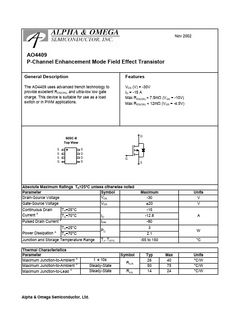
SymbolTyp Max 26405075R θJL 1424Maximum Junction-to-Lead CSteady-State°C/WThermal Characteristics ParameterUnits Maximum Junction-to-Ambient A t ≤ 10s R θJA °C/W Maximum Junction-to-Ambient A Steady-State °C/W AO4409SymbolMin TypMaxUnits BV DSS -30V -5T J =55°C-25I GSS ±100nA V GS(th)-1.4-1.9-2.7V I D(ON)80A 6.27.5T J =125°C8.211.59.512m Ωg FS 3550S V SD -0.71-1V I S-5A C iss 5270pF C oss 945pF C rss 745pF R g 2ΩQ g 100nC Q g (4.5V)51.5nC Q gs 14.5nC Q gd 23nC t D(on)14ns t r 16.5ns t D(off)76.5ns t f 37.5ns t rr 36.7ns Q rr 28nCBody Diode Reverse Recovery Time Body Diode Reverse Recovery ChargeI F =-15A, dI/dt=100A/µsDrain-Source Breakdown Voltage On state drain currentI D =-250µA, V GS =0V V GS =-10V, V DS =-5V V GS =-10V, I D =-15AReverse Transfer Capacitance I F =-15A, dI/dt=100A/µs Electrical Characteristics (T J =25°C unless otherwise noted)STATIC PARAMETERS ParameterConditions I DSS µA Gate Threshold Voltage V DS =V GS I D =-250µA V DS =-24V, V GS =0VV DS =0V, V GS =±20V Zero Gate Voltage Drain Current Gate-Body leakage current R DS(ON)Static Drain-Source On-ResistanceForward Transconductance Diode Forward Voltage m ΩV GS =-4.5V, I D =-10AI S =-1A,V GS =0V V DS =-5V, I D =-15A Turn-On Rise Time Turn-Off DelayTime V GS =-10V, V DS =-15V, R L =1Ω, R GEN =3ΩGate resistance V GS =0V, V DS =0V, f=1MHzTurn-Off Fall Time SWITCHING PARAMETERS Total Gate Charge V GS =-10V, V DS =-15V, I D =-15AGate Source Charge Maximum Body-Diode Continuous CurrentInput Capacitance Output Capacitance Turn-On DelayTime DYNAMIC PARAMETERS V GS =0V, V DS =-15V, f=1MHz Gate Drain Charge Gate Charge A: The value of R θJA is measured with the device mounted on 1in 2FR-4 board with 2oz. Copper, in a still air environment with T A =25°C. The value in any a given application depends on the user's specific board design. The current rating is based on the t ≤ 10s thermal resistance rating.B: Repetitive rating, pulse width limited by junction temperature.C. The R θJA is the sum of the thermal impedence from junction to lead R θJL and lead to ambient.D. The static characteristics in Figures 1 to 6,12,14 are obtained using 80 µs pulses, duty cycle 0.5% max.E. These tests are performed with the device mounted on 1 in 2FR-4 board with 2oz. Copper, in a still air environment with T A =25°C. The SOA curve provides a single pulse rating.。
AO4404
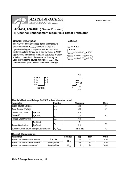
SymbolTyp Max 31405975R θJL 1624Maximum Junction-to-Lead CSteady-State°C/WThermal Characteristics ParameterUnits Maximum Junction-to-Ambient A t ≤ 10s R θJA °C/W °C/W Maximum Junction-to-Ambient A Steady-StateSymbolMin TypMaxUnits BV DSS 30V 0.0021T J =55°C5I GSS 100nA V GS(th)0.711.4V I D(ON)40A 20.524T J =125°C30362530m Ω4048m Ωg FS 1016S V SD 0.711V I S4.3A C iss 8571030pF C oss 97pF C rss 71pF R g1.4 3.6ΩQ g 9.712nC Q gs 1.63nC Q gd 3.1nC t D(on) 3.35ns t r 4.77ns t D(off)2639ns t f 4.1 6.2ns t rr 1520ns Q rr8.612nCTHIS PRODUCT HAS BEEN DESIGNED AND QUALIFIED FOR THE CONSUMER MARKET. APPLICATIONS OR USES AS CRITICAL COMPONENTS IN LIFE SUPPORT DEVICES OR SYSTEMS ARE NOT AUTHORIZED. AOS DOES NOT ASSUME ANY LIABILITY ARISING OUT OF SUCH APPLICATIONS OR USES OF ITS PRODUCTS. AOS RESERVES THE RIGHT TO IMPROVE PRODUCT DESIGN,FUNCTIONS AND RELIABILITY WITHOUT NOTICE.Gate resistanceV GS =0V, V DS =0V, f=1MHzTurn-Off Fall TimeMaximum Body-Diode Continuous CurrentInput Capacitance Output Capacitance Turn-On DelayTime DYNAMIC PARAMETERS I F =5A, dI/dt=100A/µs V GS =0V, V DS =15V, f=1MHz SWITCHING PARAMETERS Total Gate Charge V GS =4.5V, V DS =15V, I D =8.5AGate Source Charge Gate Drain Charge Turn-On Rise Time Turn-Off DelayTime V GS =10V, V DS =15V, R L =1.8Ω, R GEN =6Ωm ΩV GS =4.5V, I D =8.5A I S =1A,V GS =0V V DS =5V, I D =5AR DS(ON)Static Drain-Source On-ResistanceForward TransconductanceDiode Forward Voltage I DSS µA Gate Threshold Voltage V DS =V GS I D =250µA V DS =24V, V GS =0VV DS =0V, V GS = ±12V Zero Gate Voltage Drain Current Gate-Body leakage current Electrical Characteristics (T J =25°C unless otherwise noted)STATIC PARAMETERS ParameterConditions Body Diode Reverse Recovery Time Body Diode Reverse Recovery ChargeI F =5A, dI/dt=100A/µsDrain-Source Breakdown Voltage On state drain currentI D =250µA, V GS =0V V GS =2.5V, I D =5AV GS =4.5V, V DS =5V V GS =10V, I D =8.5AReverse Transfer Capacitance A: The value of R θJA is measured with the device mounted on 1in 2 FR-4 board with 2oz. Copper, in a still air environment with T A =25°C. The value in any a given application depends on the user's specific board design. The current rating is based on the t ≤ 10s thermal resistance rating.B: Repetitive rating, pulse width limited by junction temperature.C. The R θJA is the sum of the thermal impedence from junction to lead R θJL and lead to ambient.D. The static characteristics in Figures 1 to 6 are obtained using 80 µs pulses, duty cycle 0.5% max.E. These tests are performed with the device mounted on 1 in 2FR-4 board with 2oz. Copper, in a still air environment with T A =25°C. The SOA curve provides a single pulse rating.。
AO4924中文资料
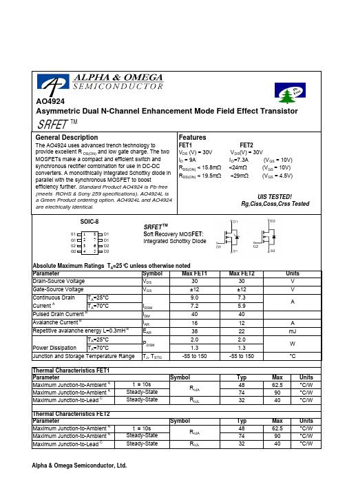
AO4924Asymmetric Dual N-Channel Enhancement Mode Field Effect TransistorAO4924SymbolMin TypMaxUnits BV DSS 30V V DS =24V, V GS =0V0.010.1T J =125°C510I GSS 0.1µA V GS(th)Gate Threshold Voltage 1.5 1.852.4V I D(ON)40A 1315.8T J =125°C20.025.015.719.5m Ωg FS 64S V SD 0.40.6V I S4.5A C iss 14501885pF C oss 224pF C rss92pF R g 1.6 3 ΩQ g (10V)24.031Q g (4.5V)12.0nC Q gs 3.9nC Q gd 4.2nC t D(on) 5.5ns t r 4.7ns t D(off)24.0ns t f 4.0ns t rr 1013ns Q rr6.8nCTHIS PRODUCT HAS BEEN DESIGNED AND QUALIFIED FOR THE CONSUMER MARKET. APPLICATIONS OR USES AS CRITICAL COMPONENTS IN LIFE SUPPORT DEVICES OR SYSTEMS ARE NOT AUTHORIZED. AOS DOES NOT ASSUME ANY LIABILITY ARISING OUT OF SUCH APPLICATIONS OR USES OF ITS PRODUCTS. AOS RESERVES THE RIGHT TO IMPROVE PRODUCT DESIGN,FUNCTIONS AND RELIABILITY WITHOUT NOTICE.Body Diode Reverse Recovery Time Body Diode Reverse Recovery ChargeI F =9A, dI/dt=300A/µsDrain-Source Breakdown Voltage On state drain currentI D =1mA, V GS =0V V GS =4.5V, V DS =5V V GS =10V, I D =9AReverse Transfer CapacitanceI F =9A, dI/dt=300A/µs V DS =V GS I D =250µA FET1 Electrical Characteristics (T J =25°C unless otherwise noted)STATIC PARAMETERS Parameter Conditions I DSS Zero Gate Voltage Drain Current mA V DS =0V, V GS = ±12V Gate-Body leakage current R DS(ON)Static Drain-Source On-ResistanceForward TransconductanceDiode Forward VoltageMaximum Body-Diode + Schottky Continuous CurrentInput Capacitance Output Capacitance DYNAMIC PARAMETERS m ΩV GS =4.5V, I D =7AI S =1A,V GS =0V V DS =5V, I D =9ATurn-On Rise Time Turn-Off DelayTime V GS =10V, V DS =15V, R L =1.7Ω, R GEN =3ΩTurn-Off Fall TimeTurn-On DelayTime Total Gate Charge V GS =10V, V DS =15V, I D =9AGate Drain Charge V GS =0V, V DS =15V, f=1MHzSWITCHING PARAMETERS Total Gate Charge Gate Source Charge Gate resistance V GS =0V, V DS =0V, f=1MHz A: The value of R θJA is measured with the device in a still air environment with T A =25°C. The power dissipation P DSM and current rating I DSM are based on T (J(MAX)=150°C, using t ≤ 10s junction-to-ambient thermal resistance.B: Repetitive rating, pulse width limited by junction temperature T J(MAX)=150°C.C. The R θJA is the sum of the thermal impedence from junction to lead R θJL and lead to ambient.D. The static characteristics in Figures 1 to 6 are obtained using <300 µs pulses, duty cycle 0.5% max.E. These tests are performed with the device mounted on 1 in 2 FR-4 board with 2oz. Copper, in a still air environment with T A =25°C. The SOA curve provides a single pulse rating. Rev0:Sept. 2006AO4924AO4924AO4924AO4924SymbolMin TypMaxUnits BV DSS 30V 1T J =55°C5I GSS 100nA V GS(th)0.711.5V I D(ON)40A 2024T J =125°C283423.529m Ωg FS 26S V SD 0.711V I S4.5A C iss 9001100pF C oss 88pF C rss 65pF R g0.95 1.5ΩQ g 1012nC Q gs 1.8nC Q gd 3.75nC t D(on) 3.2ns t r 3.5ns t D(off)21.5ns t f 2.7ns t rr 16.820ns Q rr812nCTHIS PRODUCT HAS BEEN DESIGNED AND QUALIFIED FOR THE CONSUMER MARKET. APPLICATIONS OR USES AS CRITICAL COMPONENTS IN LIFE SUPPORT DEVICES OR SYSTEMS ARE NOT AUTHORIZED. AOS DOES NOT ASSUME ANY LIABILITY ARISING OUT OF SUCH APPLICATIONS OR USES OF ITS PRODUCTS. AOS RESERVES THE RIGHT TO IMPROVE PRODUCT DESIGN,FUNCTIONS AND RELIABILITY WITHOUT NOTICE.Body Diode Reverse Recovery TimeBody Diode Reverse Recovery Charge I F =7.3A, dI/dt=100A/µsDrain-Source Breakdown Voltage On state drain currentI D =250µA, V GS =0V V GS =4.5V, V DS =5V V GS =10V, I D =7.3AReverse Transfer Capacitance FET2 Electrical Characteristics (T J =25°C unless otherwise noted)STATIC PARAMETERS ParameterConditions I DSS µA Gate Threshold Voltage V DS =V GS I D =250µA V DS =24V, V GS =0VV DS =0V, V GS = ±12V Zero Gate Voltage Drain Current Gate-Body leakage current R DS(ON)Static Drain-Source On-ResistanceForward TransconductanceDiode Forward Voltage I F =7.3A, dI/dt=100A/µsV GS =0V, V DS =15V, f=1MHz SWITCHING PARAMETERS Total Gate Charge V GS =4.5V, V DS =15V, I D =7.3AGate Source Charge Gate Drain Charge Turn-On Rise Time Turn-Off DelayTime V GS =10V, V DS =15V, R L =2Ω, R GEN =6ΩTurn-Off Fall TimeMaximum Body-Diode Continuous CurrentInput Capacitance Output Capacitance Turn-On DelayTime DYNAMIC PARAMETERS Gate resistanceV GS =0V, V DS =0V, f=1MHzm ΩV GS =4.5V, I D =6AI S =1A,V GS =0V V DS =5V, I D =7.3AA: The value of R θJA is measured with the device mounted on 1in 2FR-4 board with 2oz. Copper, in a still air environment with T A =25°C. The value in any given application depends on the user's specific board design. The current rating is based on the t ≤ 10s thermal resistance rating.B: Repetitive rating, pulse width limited by junction temperature.C. The R θJA is the sum of the thermal impedence from junction to lead R θJL and lead to ambient.D. The static characteristics in Figures 1 to 6 are obtained using <300 µs pulses, duty cycle 0.5% max.E. These tests are performed with the device mounted on 1 in 2FR-4 board with 2oz. Copper, in a still air environment with T A =25°C. The SOA curve provides a single pulse rating. Rev 0 : Sept. 2006AO4924AO4924。
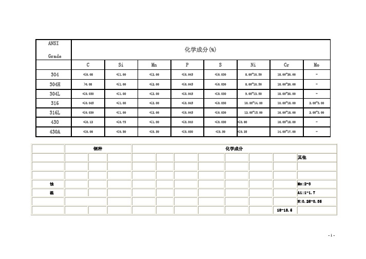
ANSI常用不锈钢材料化学成份
-1-
中国与亚洲、北美诸国(地区)以及澳大利亚的不锈钢钢号近似对照:
中国① No.
GB
中国台湾 CNS
日本 JIS
韩国 KS
印度 IS
美国 ASTM UNS
加拿大 CSA
墨西 哥 DGN
奥氏体不锈钢
1 1Cr17Mn6Ni5N
201
SUS201 STS201 10Cr17Mn6Ni4N20 201 S20100 201
-
430F S43020 430F 430F
39 1Cr17Mo
434 SUS434 STS434
-
434 S43400 434
-
40 00Cr30Mo2
447JI SUS447J1 STS447J1
-
-
-
-
-
41 00Cr27Mo
XM27 USUSXM27 STSXM27
-
XM27 S44625 -
29 0Cr18Ni11Nb
347
SUS347 STS347 04Cr18Ni10Nb40 347 S34700
30 0Cr18Ni9Cu3
XM7 SUSXM7 STSXM7
-
XM7
-
31 0Cr18Nil3Si4 XM1511 SUSXM15J1 STSXM15J1
-
XM15 S38100
309S
-
316LN
SUSJ1 STS316J1
-
-
SUS316J1L STS316J1L
-
-
SUS317 STS317
-
317
-
-
--
-
-
-
AO4404中文资料
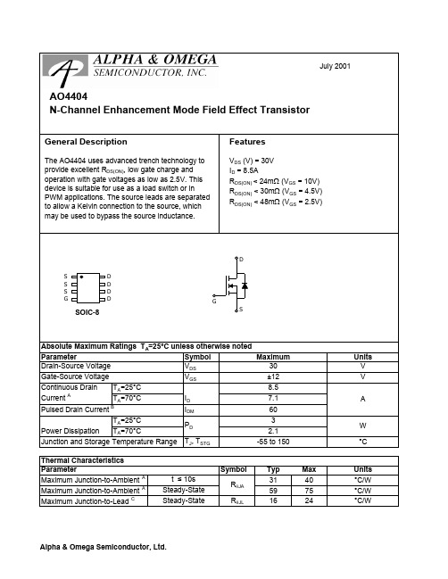
SymbolTyp Max 31405975R θJL 1624Maximum Junction-to-Ambient A Steady-State °C/W Maximum Junction-to-Lead CSteady-State°C/WThermal Characteristics ParameterUnits Maximum Junction-to-Ambient A t ≤ 10s R θJA °C/W AO4404Symbol Min TypMaxUnits BV DSS 30V 1T J =55°C5I GSS 100nA V GS(th)0.71 1.4V I D(ON)40A 20.524T J =125°C30362530m Ω4048m Ωg FS 1016S V SD 0.711V I S4.3A C iss 857pF C oss 97pF C rss71pF R g1.4ΩQ g 9.7nC Q gs1.63nC Q gd 3.1nC t D(on)14ns t r 4ns t D(off)33ns t f5ns t rr 15ns Q rr 8.6nCBody Diode Reverse Recovery Time Body Diode Reverse Recovery ChargeI F =5A, dI/dt=100A/µsDrain-Source Breakdown Voltage On state drain currentI D =250µA, V GS =0V V GS =2.5V, I D =5A V GS =4.5V, V DS =5V V GS =10V, I D =8.5AReverse Transfer Capacitance Electrical Characteristics (T J =25°C unless otherwise noted)STATIC PARAMETERS Parameter Conditions I DSS µA Gate Threshold Voltage V DS =V GS I D =250µA V DS =24V, V GS =0VV DS =0V, V GS = ±12V Zero Gate Voltage Drain Current Gate-Body leakage current R DS(ON)Static Drain-Source On-ResistanceForward TransconductanceDiode Forward Voltage m ΩV GS =4.5V, I D =8.5A I S =1A,V GS =0V V DS =5V, I D =5A I F =5A, dI/dt=100A/µs V GS =0V, V DS =15V, f=1MHz SWITCHING PARAMETERSTotal Gate ChargeV GS =4.5V, V DS =15V, I D =8.5AGate Source Charge Gate Drain Charge Turn-On Rise Time Turn-Off DelayTimeV GS =10V, V DS =15V, R L =1.8Ω, R GEN =6ΩGate resistance V GS =0V, V DS =0V, f=1MHzTurn-Off Fall Time Maximum Body-Diode Continuous CurrentInput Capacitance Output CapacitanceTurn-On DelayTime DYNAMIC PARAMETERS A: The value of R θJA is measured with the device mounted on 1in 2FR-4 board with 2oz. Copper, in a still air environment with T A =25°C. The value in any a given application depends on the user's specific board design. The current rating is based on the t ≤ 10s thermal resistance rating.B: Repetitive rating, pulse width limited by junction temperature.C. The R θJA is the sum of the thermal impedence from junction to lead R θJL and lead to ambient.D. The static characteristics in Figures 1 to 6 are obtained using 80 µs pulses, duty cycle 0.5% max.E. These tests are performed with the device mounted on 1 in 2FR-4 board with 2oz. Copper, in a still air environment with T A =25°C. The SOA curve provides a single pulse rating.。
AO4480中文资料

SymbolTyp Max 30405975R θJL 1624°C/W Maximum Junction-to-Ambient ASteady-State Maximum Junction-to-Lead CSteady-State°C/WThermal Characteristics ParameterUnits Maximum Junction-to-Ambient At ≤ 10s R θJA °C/W AO4480AO4480SymbolMin TypMaxUnits BV DSS 40V 1T J =55°C5I GSS ±100µA V GS(th)123V I D(ON)70A 9 11.5T J =125°C131215.5m Ωg FS 50S V SD 0.71V I S4A C iss 16001920pF C oss 320pFC rss 100 pFR g3.4ΩQ g (10V)22nC Q g (4.5V)10.5nC Q gs 4.2nC Q gd 4.8nC t D(on) 3.5ns t r 6ns t D(off)13.2ns t f 3.5ns t rr 31ns Q rr33nCTHIS PRODUCT HAS BEEN DESIGNED AND QUALIFIED FOR THE CONSUMER MARKET. APPLICATIONS OR USES AS CRITICAL COMPONENTS IN LIFE SUPPORT DEVICES OR SYSTEMS ARE NOT AUTHORIZED. AOS DOES NOT ASSUME ANY LIABILITY ARISING OUT OF SUCH APPLICATIONS OR USES OF ITS PRODUCTS. AOS RESERVES THE RIGHT TO IMPROVE PRODUCT DESIGN,FUNCTIONS AND RELIABILITY WITHOUT NOTICE.Gate Drain Charge V GS =0V, V DS =20V, f=1MHz SWITCHING PARAMETERS Total Gate Charge Gate Source Charge Gate resistanceV GS =0V, V DS =0V, f=1MHzTotal Gate Charge V GS =10V, V DS =20V, I D =14ATurn-On Rise Time Turn-Off DelayTime V GS =10V, V DS =20V, R L =1.5Ω, R GEN =3ΩTurn-Off Fall TimeTurn-On DelayTime m ΩV GS =4.5V, I D =5AI S =1A,V GS =0V V DS =5V, I D =14AMaximum Body-Diode Continuous CurrentInput Capacitance Output Capacitance DYNAMIC PARAMETERS R DS(ON)Static Drain-Source On-ResistanceForward TransconductanceDiode Forward VoltageI DSS uA Gate Threshold Voltage V DS =V GS I D =250µA V DS =32V, V GS =0VV DS =0V, V GS = ±20V Zero Gate Voltage Drain Current Gate-Body leakage current Electrical Characteristics (T J =25°C unless otherwise noted)STATIC PARAMETERS Parameter Conditions Body Diode Reverse Recovery TimeBody Diode Reverse Recovery Charge I F =14A, dI/dt=100A/µsDrain-Source Breakdown Voltage On state drain currentI D =250uA, V GS =0V V GS =10V, V DS =5V V GS =10V, I D =14AReverse Transfer Capacitance I F =14A, dI/dt=100A/µsA: The value of R θJA is measured with the device mounted on 1in 2 FR-4 board with 2oz. Copper, in a still air environment with T A =25°C. The value in any given application depends on the user's specific board design. B: Repetitive rating, pulse width limited by junction temperature.C. The R θJA is the sum of the thermal impedence from junction to lead R θJL and lead to ambient.D. The static characteristics in Figures 1 to 6 are obtained using <300 µs pulses, duty cycle 0.5% max.E. These tests are performed with the device mounted on 1 in 2 FR-4 board with 2oz. Copper, in a still air environment with T A =25°C. The SOA curve provides a single pulse rating.F. The current rating is based on the t ≤ 10s junction to ambient thermal resistance rating.Rev0: Oct 2006AO4480AO4480。
AO4406AL中文资料
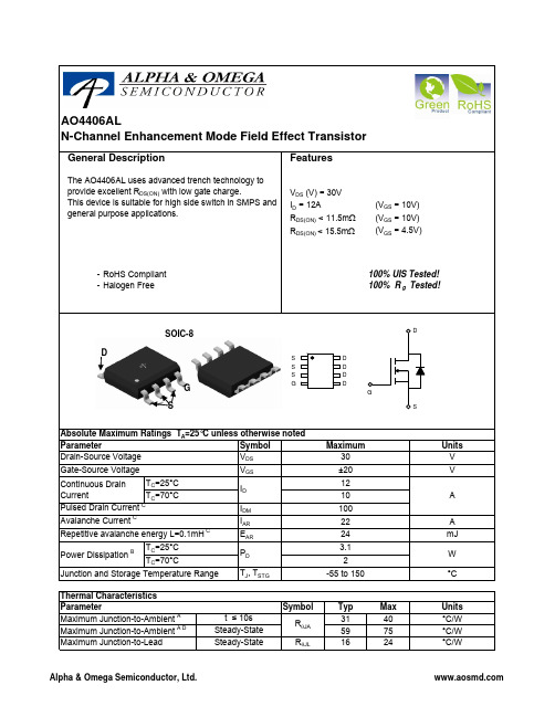
SymbolTyp Max 31405975R θJL 1624Thermal Characteristics t ≤ 10s °C/W ParameterR θJA AO4406ALAbsolute Maximum Ratings T A =25°C unless otherwise noted Maximum Junction-to-LeadSteady-State°C/WSteady-State °C/W Maximum Junction-to-Ambient A D Units Maximum Junction-to-Ambient A SOIC-8G SDSymbolMin TypMaxUnits BV DSS 30V V DS =30V, V GS =0V1T J =55°C5I GSS 100nA V GS(th)Gate Threshold Voltage 1.5 1.92.5V I D(ON)100A 9.511.5T J =125°C141712.515.5m Ωg FS 45S V SD 0.751V I S4A C iss 610760910pF C oss 88125160pF C rss 4070100pF R g0.8 1.6 2.4ΩQ g (10V)111417nC Q g (4.5V)5 6.68nC Q gs 1.9 2.4 2.9nC Q gd 1.83 4.2nC t D(on) 4.4ns t r 9ns t D(off)17ns t f 6ns t rr 5.678ns Q rr6.489.6nCRev 0 : Oct-08COMPONENTS IN LIFE SUPPORT DEVICES OR SYSTEMS ARE NOT AUTHORIZED. AOS DOES NOT ASSUME ANY LIABILITY ARISING OUT OF SUCH APPLICATIONS OR USES OF ITS PRODUCTS. AOS RESERVES THE RIGHT TO IMPROVE PRODUCT DESIGN,FUNCTIONS AND RELIABILITY WITHOUT NOTICE.Body Diode Reverse Recovery Charge I F =12A, dI/dt=500A/µsMaximum Body-Diode Continuous CurrentInput Capacitance Output CapacitanceTurn-On DelayTime DYNAMIC PARAMETERS Turn-On Rise Time Turn-Off DelayTime V GS =10V, V DS =15V, R L =1.25Ω, R GEN =3ΩGate resistanceV GS =0V, V DS =0V, f=1MHzTurn-Off Fall TimeTotal Gate Charge V GS =10V, V DS =15V, I D =12AGate Source Charge Gate Drain Charge Total Gate Charge m ΩI S =1A,V GS =0V V DS =5V, I D =12AV GS =4.5V, I D =10AForward TransconductanceDiode Forward VoltageR DS(ON)Static Drain-Source On-ResistanceI DSS µA V DS =V GS I D =250µA V DS =0V, V GS = ±20V Zero Gate Voltage Drain Current Gate-Body leakage current Electrical Characteristics (T J =25°C unless otherwise noted)STATIC PARAMETERS ParameterConditions Body Diode Reverse Recovery TimeDrain-Source Breakdown Voltage On state drain currentI D =250µA, V GS =0V V GS =10V, V DS =5V V GS =10V, I D =12AReverse Transfer Capacitance I F =12A, dI/dt=500A/µsV GS =0V, V DS =15V, f=1MHz SWITCHING PARAMETERS A. The value of R θJA is measured with the device mounted on 1in 2 FR-4 board with 2oz. Copper, in a still air environment with T A =25°C. The value in any given application depends on the user's specific board design.B. The power dissipation P D is based on T J(MAX)=150°C, using ≤ 10s junction-to-ambient thermal resistance.C. Repetitive rating, pulse width limited by junction temperature T J(MAX)=150°C. Ratings are based on low frequency and duty cycles to keep initialT J =25°C.D. The R θJA is the sum of the thermal impedence from junction to lead R θJL and lead to ambient.E. The static characteristics in Figures 1 to 6 are obtained using <300µs pulses, duty cycle 0.5% max.F. These curves are based on the junction-to-ambient thermal impedence which is measured with the device mounted on 1in 2FR-4 board with 2oz. Copper, assuming a maximum junction temperature of T J(MAX)=150°C. The SOA curve provides a single pulse rating.TYPICAL ELECTRICAL AND THERMAL CHARACTERISTICS11.522.533.54V GS (Volts)Figure 2: Transfer Characteristics (Note E)2040608010012345V DS (Volts)Fig 1: On-Region Characteristics (Note E)I D (A )TYPICAL ELECTRICAL AND THERMAL CHARACTERISTICS2468102468101214Q g (nC)Figure 7: Gate-Charge Characteristics V G S (V o l t s )20040060080010001200051015202530V DS (Volts)Figure 8: Capacitance Characteristics C a p a c i t a n c e (p F )TYPICAL ELECTRICAL AND THERMAL CHARACTERISTICSAO4406ALVdsChargeGate Charge Test Circuit & WaveformResistive Switching Test Circuit & WaveformsVddVdsIdVgsBV I Unclamped Inductive Switching (UIS) Test Circuit & WaveformsARDSS2E = 1/2 LI VddAR AR。
全自动生化仪简介

OLYMPUS AU系列全自动生化仪
AU400
AU2700
AU640
AU系列各型号生化仪对比
机型
试剂位 R1/R2
项目 速度 样本 (双) 无 ISE (ul)
R1 (ul)
R2 (ul)
反应液 (ul)
AU400 48/48
AU600 AU640
48/48 48/48
AU2700 48/48
CX9
24
33 900 3-25
LX20
41
70 800 3-25
Beckman系列生化仪性能特点
光源采用长寿闪烁式氙灯,无需保养和 更换。
比色杯直径0.5cm,因数法检测时需要在 理论因数的基础上*2。
酶类项目采用因数法时免校正。 使用标准液定标一个项目,需要一个标
准液位置,不能重复使用。
AU400采用干式空气浴,AU640采用恒温液循 环加温方式,升温均匀。
带冷藏的48位试剂盘,R1/R2试剂位置可随意 设置,避免R1/R2不同盘造成的试剂位浪费。 单数为外圈,放30ml小瓶,双数为内圈,可放 60ml的大瓶。
除AU600外,都具有样本预稀释(5-100 倍)功能,可以检测高浓度标本,并且 可以通过预稀释降低试剂用量。
日立系列生化仪性能特点
从紧凑型的7020到组合式的7600,都具有强大的功能, 可以满足各种项目的检测需要。
开放式的试剂系统。试剂和样本微量化。
灵活的反应时间,可自由控制。
仪器线性宽,量程0-32000。
同样一个项目可以同时输入血清和尿液两套参数(不 占试剂通道)。
全反应过程监测,可以察看任意时间反应曲线 和吸光度,便于发现和解决问题。
AO4420中文资料
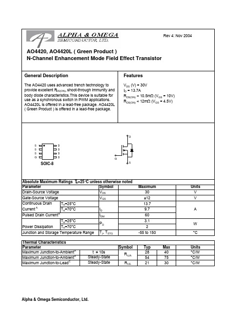
SymbolTyp Max 28405475R θJL2130Maximum Junction-to-LeadCSteady-State°C/WThermal Characteristics ParameterUnits Maximum Junction-to-AmbientAt ≤ 10s R θJA °C/W °C/W Maximum Junction-to-AmbientASteady-State AO4420, AO4420L ( Green Product )SymbolMin TypMaxUnits BV DSS 30V 0.0041T J =55°C5I GSS 100nA V GS(th)0.6 1.12V I D(ON)40A 8.310.5T J =125°C12.5159.712m Ωg FS 3037S V SD 0.761V I S5A DYNAMIC PARAMETERS C iss 36564050pF C oss 256pF C rss 168pF R g 0.86 1.1ΩSWITCHING PARAMETERS Q g (4.5V)30.536nC Q gs 4.6nC Q gd 8.6nC t D(on) 5.59ns t r 3.47ns t D(off)49.875ns t f 5.911ns t rr 22.528ns Q rr 12.516nCTHIS PRODUCT HAS BEEN DESIGNED AND QUALIFIED FOR THE CONSUMER MARKET. APPLICATIONS OR USES AS CRITICAL COMPONENTS IN LIFE SUPPORT DEVICES OR SYSTEMS ARE NOT AUTHORIZED. AOS DOES NOT ASSUME ANY LIABILITY ARISING OUT OF SUCH APPLICATIONS OR USES OF ITS PRODUCTS. AOS RESERVES THE RIGHT TO IMPROVE PRODUCT DESIGN,FUNCTIONS AND RELIABILITY WITHOUT NOTICE.Gate Drain Charge Body Diode Reverse Recovery ChargeI F =13.7A, dI/dt=100A/µsV GS =0V, V DS =0V, f=1MHzTurn-On Rise Time Turn-Off DelayTime V GS =10V, V DS =15V, R L =1.1Ω, R GEN =0ΩTurn-Off Fall Time Body Diode Reverse Recovery Time Total Gate Charge Input Capacitance I F =13.7A, dI/dt=100A/µs On state drain currentForward Transconductance Diode Forward Voltage I S =1A,V GS =0V V GS =4.5V, V DS =5V Turn-On DelayTime V GS =10V, V DS =15V, I D =13.7AElectrical Characteristics (T J =25°C unless otherwise noted)STATIC PARAMETERS ParameterConditions I DSS µA Gate Threshold Voltage Drain-Source Breakdown Voltage I D =250µA, V GS =0V Zero Gate Voltage Drain Current Gate-Body leakage current V DS =V GS I D =250µA V DS =24V, V GS =0VV DS =0V, V GS = ±12V R DS(ON)Static Drain-Source On-Resistancem ΩV GS =4.5V, I D =12.7AV GS =10V, ID=13.7AGate Source Charge Gate resistance Reverse Transfer Capacitance V DS =5V, I D =13.7A Output Capacitance Maximum Body-Diode Continuous CurrentV GS =0V, V DS =15V, f=1MHz A: The value of R θJA is measured with the device mounted on 1in 2FR-4 board with 2oz. Copper, in a still air environment with T A =25°C. The value in any a given application depends on the user's specific board design. The current rating is based on the t ≤ 10s thermal resistance rating.B: Repetitive rating, pulse width limited by junction temperature.C. The R θJA is the sum of the thermal impedence from junction to lead R θJL and lead to ambient.D. The static characteristics in Figures 1 to 6 are obtained using 80 µs pulses, duty cycle 0.5% max.E. These tests are performed with the device mounted on 1 in 2FR-4 board with 2oz. Copper, in a still air environment with T A =25°C. The SOA curve provides a single pulse rating.元器件交易网。
AO4604 规格书
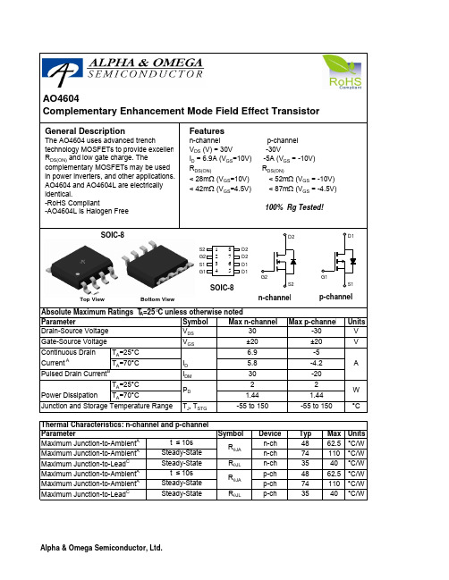
Symbol Symbol DeviceTyp Max Units n-ch 4862.5°C/W n-ch 74110°C/W R θJL n-ch 3540°C/Wp-ch 4862.5°C/W p-ch 74110°C/W R θJLp-ch3540°C/WMaximum Junction-to-LeadCSteady-State Maximum Junction-to-AmbientAt ≤ 10s R θJA Maximum Junction-to-AmbientASteady-State Steady-State Absolute Maximum Ratings T A =25°C unless otherwise notedParameter Thermal Characteristics: n-channel and p-channel Maximum Junction-to-LeadCSteady-State ParameterMaximum Junction-to-AmbientAt ≤ 10s R θJA Maximum Junction-to-AmbientAAO4604SOIC-8Top View Bottom ViewAlpha & Omega Semiconductor, Ltd.SymbolMin Typ Max Units BV DSS 30V0.0041T J =55°C5I GSS 100nA V GS(th)1 1.93V I D(ON)20A22.528T J =125°C31.33834.542m Ωg FS 1015.4S V SD 0.761V I S3A C iss 680820pF C oss 102pF C rss 77pFR g1.22ΩQ g (10V)13.8417nC Q g (4.5V) 6.748.1nC Q gs 1.82nC Q gd 3.2nC t D(on) 4.6ns t r 4.1ns t D(off)20.6ns t f 5.2nst rr 16.520ns Q rr7.8nCTHIS PRODUCT HAS BEEN DESIGNED AND QUALIFIED FOR THE CONSUMER MARKET. APPLICATIONS OR USES AS CRITICAL COMPONENTS IN LIFE SUPPORT DEVICES OR SYSTEMS ARE NOT AUTHORIZED. AOS DOES NOT ASSUME ANY LIABILITY ARISING OUT OF SUCH APPLICATIONS OR USES OF ITS PRODUCTS. AOS RESERVES THE RIGHT TO IMPROVE PRODUCT DESIGN,FUNCTIONS AND RELIABILITY WITHOUT NOTICEI F =6.9A, dI/dt=100A/µs I F =6.9A, dI/dt=100A/µsN-CHANNEL: Electrical Characteristics (T J =25°C unless otherwise noted)Parameter Conditions STATIC PARAMETERS Drain-Source Breakdown Voltage I D =250µA, V GS =0V I DSS Zero Gate Voltage Drain Current V DS =24V, V GS =0VµA Gate-Body leakage current V DS =0V, V GS =±20V Gate Threshold Voltage V DS =V GS I D =250µA On state drain currentV GS =4.5V, V DS =5V R DS(ON)Static Drain-Source On-ResistanceV GS =10V, I D =6.9Am ΩV GS =4.5V, I D =5.0AV GS =0V, V DS =0V, f=1MHzForward Transconductance V DS =5V, I D =6.9A Diode Forward VoltageI S =1AMaximum Body-Diode Continuous CurrentDYNAMIC PARAMETERSInput Capacitance V GS =0V, V DS =15V, f=1MHz Output CapacitanceGate Drain Charge Reverse Transfer Capacitance Turn-On Rise Time Turn-Off DelayTime Gate resistanceBody Diode Reverse Recovery Time Body Diode Reverse Recovery ChargeTurn-Off Fall TimeSWITCHING PARAMETERSTotal Gate Charge Total Gate Charge Gate Source Charge Turn-On DelayTime V GS =10V, V DS =15V, R L =2.2Ω,R GEN =3ΩV GS =10V, V DS =15V, I D =6.9AA: The value of R θJA is measured with the device mounted on 1in 2FR-4 board with 2oz. Copper, in a still air environment with T A =25°C. The value in any a given application depends on the user's specific board design. The current rating is based on the t ≤ 10s thermal resistance rating.B: Repetitive rating, pulse width limited by junction temperature.C. The R θJA is the sum of the thermal impedence from junction to lead R θJL and lead to ambient.D. The static characteristics in Figures 1 to 6 are obtained using 80 µs pulses, duty cycle 0.5% max.E. These tests are performed with the device mounted on 1 in 2FR-4 board with 2oz. Copper, in a still air environment with T A =25°C. The SOA curve provides a single pulse rating.Rev 4: Jan 2009N-CHANNEL: TYPICAL ELECTRICAL AND THERMAL CHARACTERISTICSVdsCharge Gate Charge Test Circuit & WaveformD iode R ecovery TeVVddV ddV ddV V90%R esistive S w itch ing Te st C ircuit & W avefo rm sSymbolMin Typ Max Units BV DSS -30V-1T J =55°C-5I GSS ±100nA V GS(th)-1-1.8-3V I D(ON)-20A 3952T J =125°C54706787m Ωg FS 68.6S V SD -0.77-1V I S-2.8A C iss 700900pF C oss 120pF C rss 75pFR g1015ΩQ g (10V)14.719nC Q g (4.5V)7.610nC Q gs 2nC Q gd 3.8nC t D(on)8.3ns t r 5ns t D(off)29ns t f 14nst rr 23.530ns Q rr13.4nCTHIS PRODUCT HAS BEEN DESIGNED AND QUALIFIED FOR THE CONSUMER MARKET. APPLICATIONS OR USES AS CRITICAL COMPONENTS IN LIFE SUPPORT DEVICES OR SYSTEMS ARE NOT AUTHORIZED. AOS DOES NOT ASSUME ANY LIABILITY ARISING OUT OF SUCH APPLICATIONS OR USES OF ITS PRODUCTS. AOS RESERVES THE RIGHT TO IMPROVE PRODUCT DESIGN,FUNCTIONS AND RELIABILITY WITHOUT NOTICEDYNAMIC PARAMETERS Maximum Body-Diode Continuous CurrentGate resistanceV GS =0V, V DS =0V, f=1MHzV GS =0V, V DS =-15V, f=1MHz Input Capacitance Output CapacitanceTurn-On Rise Time Turn-Off DelayTime V GS =-10V, V DS =-15V, R L =3Ω,R GEN =3ΩTurn-Off Fall TimeTurn-On DelayTime SWITCHING PARAMETERSTotal Gate Charge (4.5V)Gate Source Charge Gate Drain Charge Total Gate Charge (10V)V GS =-10V, V DS =-15V, I D =-5Am ΩV GS =-4.5V, I D =-4AI S =-1A,V GS =0VV DS =-5V, I D =-5A R DS(ON)Static Drain-Source On-ResistanceForward Transconductance Diode Forward VoltageI DSS µA Gate Threshold Voltage V DS =V GS I D =-250µA V DS =-24V, V GS =0VV DS =0V, V GS =±20V Zero Gate Voltage Drain Current Gate-Body leakage current P-CHANNEL: Electrical Characteristics (T J =25°C unless otherwise noted)STATIC PARAMETERS ParameterConditions Body Diode Reverse Recovery TimeBody Diode Reverse Recovery Charge I F =-5A, dI/dt=100A/µsDrain-Source Breakdown Voltage On state drain currentI D =-250µA, V GS =0V V GS =-4.5V, V DS =-5V V GS =-10V, I D =-5AReverse Transfer Capacitance I F =-5A, dI/dt=100A/µsA: The value of R θJA is measured with the device mounted on 1in 2FR-4 board with 2oz. Copper, in a still air environment with T A =25°C. The value in any a given application depends on the user's specific board design. The current rating is based on the t ≤ 10s thermal resistance rating.B: Repetitive rating, pulse width limited by junction temperature.C. The R θJA is the sum of the thermal impedence from junction to lead R θJL and lead to ambient.D. The static characteristics in Figures 1 to 6,12,14 are obtained using 80 µs pulses, duty cycle 0.5% max.E. These tests are performed with the device mounted on 1 in 2FR-4 board with 2oz. Copper, in a still air environment with T A =25°C. The SOA curve provides a single pulse rating.Rev 4: Jan 2009VdsChargeGate Charge Test Circuit & WaveformDiode R V Vdd V dd V Resistive Sw itching Test C ircuit & W aveform sV 90%10%。
AO4407A中文资料
AO4407A中⽂资料ParameterSymbolTyp Max t ≤ 10s 3240Steady State 6075Steady StateR θJL 1724Maximum Junction-to-Lead C°C/WThermal Characteristics Units Maximum Junction-to-Ambient A °C/W Maximum Junction-to-Ambient A °C/W R θJAAO4407AP-Channel Enhancement Mode Field Effect TransistorAO4407ASymbolMin TypMaxUnits BV DSS -30V -10T J = 55°C-50I GSS ±100nA V GS(th)-1.7-2.3-3V I D(ON)-60A8.511T J =125°C11.51510132738g FS 21S V SD -0.7-1V I S-3A C iss 20602600pF C oss 370pF C rss 295pF R g2.43.6?Q g 3039nC Q gs 4.6nC Q gd 10nC t D(on)11ns t r 9.4ns t D(off)24ns t f 12ns t rr 3040ns Q rr22nC THIS PRODUCT HAS BEEN DESIGNED AND QUALIFIED FOR THE CONSUMER MARKET. APPLICATIONS OR USES AS CRITICAL COMPONENTS IN LIFE SUPPORT DEVICES OR SYSTEMS ARE NOT AUTHORIZED. AOS DOES NOT ASSUME ANY LIABILITY ARISING OUT OF SUCH APPLICATIONS OR USES OF ITS PRODUCTS. AOS RESERVES THE RIGHT TO IMPROVE PRODUCT DESIGN,FUNCTIONS AND RELIABILITY WITHOUT NOTICE.V GS =0V, V DS =-15V, f=1MHz Input Capacitance Output Capacitance Turn-On Rise Time Turn-Off DelayTime V GS =-10V, V DS =-15V, R L =1.25?, R GEN =3?Turn-Off Fall TimeTurn-On DelayTime m ?SWITCHING PARAMETERS Gate Source Charge Gate Drain Charge Total Gate Charge V GS =-10V, V DS =-15V, I D =-12ADYNAMIC PARAMETERS Maximum Body-Diode Continuous CurrentGate resistanceV GS =0V, V DS =0V, f=1MHzV GS = -5V, I D = -10AI S = -1A,V GS = 0V V DS = -5V, I D = -10AV GS = -10V, I D = -12A R DS(ON)Static Drain-Source On-ResistanceForward TransconductanceDiode Forward VoltageI DSS µA Gate Threshold Voltage V DS = V GS I D = -250µA V DS = -30V, V GS = 0VV DS = 0V, V GS = ±25V Zero Gate Voltage Drain Current Gate-Body leakage current Electrical Characteristics (T J =25°C unless otherwise noted)STATIC PARAMETERS Parameter ConditionsBody Diode Reverse Recovery TimeBody Diode Reverse Recovery Charge I F =-12A, dI/dt=100A/µsDrain-Source Breakdown Voltage On state drain currentI D = -250µA, V GS = 0V V GS = -10V, V DS = -5V V GS = -20V, I D = -12AReverse Transfer Capacitance I F =-12A, dI/dt=100A/µsA: The value of R θJA is measured with the device mounted on 1 in 2 FR-4 board with 2oz. Copper, in a still air environment with T A = 25°C. The value in any given application depends on the user's specific board design. The current rating is based on the t ≤ 10s thermal resistance rating.B: Repetitive rating, pulse width limited by junction temperature.C. The R θJA is the sum of the thermal impedence from junction to lead R θJL and lead to ambient.D. The static characteristics in Figures 1 to 6 are obtained using < 300µs pulses, duty cycle 0.5% max.E. These tests are performed with the device mounted on 1 in 2 FR-4 board with 2oz. Copper, in a still air environment with T A =25°C. The SOA curve provides a single pulse rating.F. The current rating is based on the t ≤ 10s thermal resistance rating.G. E AR and I AR ratings are based on low frequency and duty cycles to keep T j =25C.Rev3: Jan 2008AO4407AAO4407A。
CS5460A中文数据手册
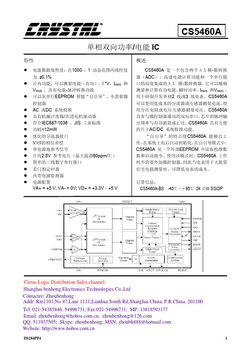
l 片内功能:可以测量电能(有功),I *V,IRMS 和 VRMS ,具有电能-脉冲转换功能
l 可以从串行EEPROM 智能“自引导”,不需要微 控制器
l AC 或DC 系统校准 l 具有机械计度器/步进电机驱动器 l 符合IEC687/1036 ,JIS 工业标准 l 功耗<12mW l 优化的分流器接口 l V对I的相位补偿 l 单电源地参考信号 l 片内2.5V 参考电压(最大温漂60ppm/℃) l 简单的三线数字串行接口 l 看门狗定时器 l 内带电源监视器 l 电源配置
VA+ = +5 V; VA- = 0V; VD+ = +3.3V~+5 V
概述
CS5460A 是一个包含两个ΔΣ模-数转换 器(ADC)、高速电能计算功能和一个串行接 口的高度集成的ΔΣ 模-数转换器。它可以精确 测量和计算有功电能、瞬时功率、IRMS 和VRMS , 用于研制开发单相2 线或3 线电表。CS5460A 可以使用低成本的分流器或互感器测量电流,使 用分压电阻或电压互感器测量电压。CS5460A 具有与微控制器通讯的双向串口,芯片的脉冲输 出频率与有功能量成正比。CS5460A 具有方便 的片上AC/DC 系统校准功能。
cs5460a单相双向功率电能ic特性rms具有电能脉冲转换功能可以从串行eeprom智能自引导不需要微控制器ac或dc系统校准符合iec6871036jis工业标准片内25v参考电压最大温漂60ppm电源配置va0v
高压直流电源400A说明书
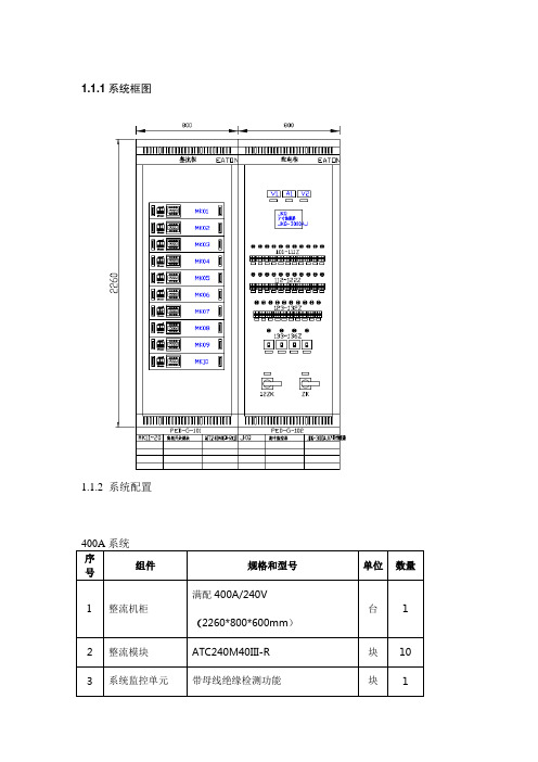
1.1.1系统框图1.1.2 系统配置1.3主要技术指标1.4系统主要功能伊顿高压直流产品由整流柜和配电柜组成,整流柜实现交流电的引入以及整流输出额定电压240V的直流。
直流屏实现电力分配,给不同的负载提供相应的电力输出。
同时在直流屏内配置集中监控单元,来完成对整个系统参数的监测。
蓄电池通过开关与熔丝的组合来引入到配电柜中。
单路交流检测电路:单路交流检测回路由交流状态监测单元实现。
正常运行时,三相交流电处于相对平衡的状态,三相交流电中心点与零线之间无电势差,内部继电器J1不动作,交流故障监测单元内的告警继电器J3的线圈通过J1的常闭接点接于零线与火线间,同时LED发光点亮,指示交流电源正常。
当交流发生缺相或三相严重不平衡时,三相交流电中心点与零线之间产生电势差,内部继电器J1得电动作,其常闭接点断开,使得内部继电器J3线圈失电,J3常闭接点闭合,发出故障告警信号,同时LED熄灭,指示交流电源故障。
✓防雷保护电路:雷击分为直击雷和感应雷两种,线路直接遭雷击时,电缆中流过很大电流,同时引起数千伏的过电压直接加到线路装置和电源设备上,持续时间达若十微秒,直接危害用电设备。
感应雷通过雷云之间或雷云对地的放电,在附近的电缆或用电设备上产生感应过电压,危害用电设备的安全。
因此必须要在交流配电单元端加装防雷器。
我司直流电源柜设有C级及D级防雷,C级防雷设在交流配电单元入口,选用的防雷器为世界名牌防雷产品,通流量为40kA,动作时间小于25ns,D级防雷设在充电模块内,通流量为10kA,动作时间小于25ns,可以有效地将雷电引入大地,将雷电的危害降至最小。
当防雷器故障时,C级防雷器的工作状态窗口由绿变红,提醒更换防雷模块,防雷模块插拔方便,易于更换。
✓雷击浪涌吸收器:雷击浪涌吸收器具有防雷和抑制电网瞬间过压双重功能,最大通流量40KA,动作时间小于25ns。
由下图可见,相线与相线之间,相线与零线之间的瞬间干扰脉冲均可被压敏电阻和气体放电组吸收。
AO4410中文资料

SymbolTyp Max 31405975R θJL 1624Maximum Junction-to-Ambient A Steady-State °C/W Maximum Junction-to-Lead CSteady-State°C/WThermal Characteristics ParameterUnits Maximum Junction-to-Ambient A t ≤ 10s R θJA °C/W AO4410AO4410SymbolMin TypMaxUnits BV DSS 30V 0.0051T J =55°C5I GSS 100nA V GS(th)0.8 1.11.5V I D(ON)80A 4.7 5.5T J =125°C6.47.45.2 6.2m Ωg FS 102S V SD 0.641V I S4.5A C iss 913010500pF C oss 625pF C rss 387pF R g0.40.5ΩQ g (4.5V)72.485nC Q gs 13.4nC Q gd 16.8nC t D(on)1115ns t r 711ns t D(off)99135ns t f 1319.5ns t rr 3340ns Q rr22.230nCTHIS PRODUCT HAS BEEN DESIGNED AND QUALIFIED FOR THE CONSUMER MARKET. APPLICATIONS OR USES AS CRITICAL COMPONENTS IN LIFE SUPPORT DEVICES OR SYSTEMS ARE NOT AUTHORIZED. AOS DOES NOT ASSUME ANY LIABILITY ARISING OUT OF SUCH APPLICATIONS OR USES OF ITS PRODUCTS. AOS RESERVES THE RIGHT TO IMPROVE PRODUCT DESIGN,FUNCTIONS AND RELIABILITY WITHOUT NOTICE.Body Diode Reverse Recovery TimeBody Diode Reverse Recovery Charge I F =18A, dI/dt=100A/µsDrain-Source Breakdown Voltage On state drain currentI D =250µA, V GS =0V V GS =4.5V, V DS =5V V GS =10V, I D =18AReverse Transfer Capacitance I F =18A, dI/dt=100A/µsElectrical Characteristics (T J =25°C unless otherwise noted)STATIC PARAMETERS ParameterConditions I DSS µA Gate Threshold Voltage V DS =V GS I D =250µA V DS =24V, V GS =0VV DS =0V, V GS = ±12V Zero Gate Voltage Drain Current Gate-Body leakage current R DS(ON)Static Drain-Source On-ResistanceForward TransconductanceDiode Forward Voltage Maximum Body-Diode Continuous CurrentInput Capacitance Output Capacitance DYNAMIC PARAMETERS m ΩV GS =4.5V, I D =15AI S =1A,V GS =0V V DS =5V, I D =18ATurn-On Rise Time Turn-Off DelayTime V GS =10V, V DS =15V, R L =0.83Ω, R GEN =3ΩTurn-Off Fall TimeTurn-On DelayTime Gate Drain Charge V GS =0V, V DS =15V, f=1MHz SWITCHING PARAMETERS Total Gate Charge Gate Source Charge Gate resistanceV GS =0V, V DS =0V, f=1MHzV GS =10V, V DS =15V, I D =18AA: The value of R θJA is measured with the device mounted on 1in 2 FR-4 board with 2oz. Copper, in a still air environment with T A =25°C. The value in any given application depends on the user's specific board design. The current rating is based on the t ≤ 10s thermal resistance rating.B: Repetitive rating, pulse width limited by junction temperature.C. The R θJA is the sum of the thermal impedence from junction to lead R θJL and lead to ambient.D. The static characteristics in Figures 1 to 6 are obtained using 80 µs pulses, duty cycle 0.5% max.E. These tests are performed with the device mounted on 1 in 2FR-4 board with 2oz. Copper, in a still air environment with T A =25°C. The SOA curve provides a single pulse rating. Rev 4 : May 2005AO4410AO4410。
AO4407A中文资料
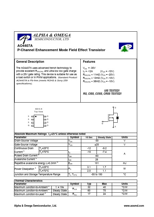
ParameterSymbolTyp Max t ≤ 10s 3240Steady State 6075Steady StateR θJL 1724Maximum Junction-to-Lead C°C/WThermal Characteristics Units Maximum Junction-to-Ambient A °C/W Maximum Junction-to-Ambient A °C/W R θJA AO4407AP-Channel Enhancement Mode Field Effect TransistorAO4407ASymbolMin TypMaxUnits BV DSS -30V -10T J = 55°C-50I GSS ±100nA V GS(th)-1.7-2.3-3V I D(ON)-60A8.511T J =125°C11.51510132738g FS 21S V SD -0.7-1V I S-3A C iss 20602600pF C oss 370pF C rss 295pF R g2.43.6ΩQ g 3039nC Q gs 4.6nC Q gd 10nC t D(on)11ns t r 9.4ns t D(off)24ns t f 12ns t rr 3040ns Q rr22nC THIS PRODUCT HAS BEEN DESIGNED AND QUALIFIED FOR THE CONSUMER MARKET. APPLICATIONS OR USES AS CRITICAL COMPONENTS IN LIFE SUPPORT DEVICES OR SYSTEMS ARE NOT AUTHORIZED. AOS DOES NOT ASSUME ANY LIABILITY ARISING OUT OF SUCH APPLICATIONS OR USES OF ITS PRODUCTS. AOS RESERVES THE RIGHT TO IMPROVE PRODUCT DESIGN,FUNCTIONS AND RELIABILITY WITHOUT NOTICE.V GS =0V, V DS =-15V, f=1MHz Input Capacitance Output Capacitance Turn-On Rise Time Turn-Off DelayTime V GS =-10V, V DS =-15V, R L =1.25Ω, R GEN =3ΩTurn-Off Fall TimeTurn-On DelayTime m ΩSWITCHING PARAMETERS Gate Source Charge Gate Drain Charge Total Gate Charge V GS =-10V, V DS =-15V, I D =-12ADYNAMIC PARAMETERS Maximum Body-Diode Continuous CurrentGate resistanceV GS =0V, V DS =0V, f=1MHzV GS = -5V, I D = -10AI S = -1A,V GS = 0V V DS = -5V, I D = -10AV GS = -10V, I D = -12A R DS(ON)Static Drain-Source On-ResistanceForward TransconductanceDiode Forward VoltageI DSS µA Gate Threshold Voltage V DS = V GS I D = -250µA V DS = -30V, V GS = 0VV DS = 0V, V GS = ±25V Zero Gate Voltage Drain Current Gate-Body leakage current Electrical Characteristics (T J =25°C unless otherwise noted)STATIC PARAMETERS Parameter ConditionsBody Diode Reverse Recovery TimeBody Diode Reverse Recovery Charge I F =-12A, dI/dt=100A/µsDrain-Source Breakdown Voltage On state drain currentI D = -250µA, V GS = 0V V GS = -10V, V DS = -5V V GS = -20V, I D = -12AReverse Transfer Capacitance I F =-12A, dI/dt=100A/µsA: The value of R θJA is measured with the device mounted on 1 in 2 FR-4 board with 2oz. Copper, in a still air environment with T A = 25°C. The value in any given application depends on the user's specific board design. The current rating is based on the t ≤ 10s thermal resistance rating.B: Repetitive rating, pulse width limited by junction temperature.C. The R θJA is the sum of the thermal impedence from junction to lead R θJL and lead to ambient.D. The static characteristics in Figures 1 to 6 are obtained using < 300µs pulses, duty cycle 0.5% max.E. These tests are performed with the device mounted on 1 in 2 FR-4 board with 2oz. Copper, in a still air environment with T A =25°C. The SOA curve provides a single pulse rating.F. The current rating is based on the t ≤ 10s thermal resistance rating.G. E AR and I AR ratings are based on low frequency and duty cycles to keep T j =25C.Rev3: Jan 2008AO4407AAO4407A。
AO4444中文资料
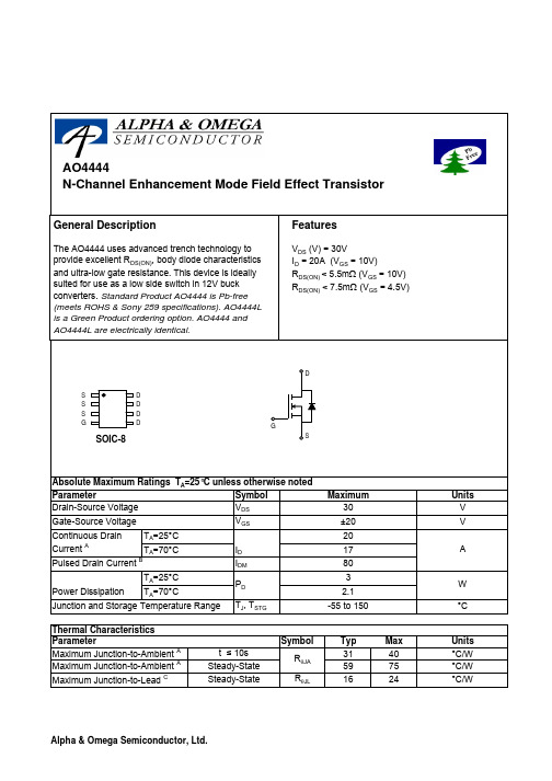
SymbolTyp Max 31405975R θJL 1624Maximum Junction-to-Ambient A Steady-State °C/W Maximum Junction-to-Lead CSteady-State°C/WThermal Characteristics ParameterUnits Maximum Junction-to-Ambient A t ≤ 10s R θJA °C/W AO4444AO4444SymbolMin TypMaxUnits BV DSS 30V 1T J =55°C5I GSS 100nA V GS(th)1 1.83V I D(ON)60A 3.9 5.5T J =125°C5.16.25.17.5m Ωg FS 106S V SD 0.721V I S4A C iss 32003840pF C oss 590pF C rss 414pF R g0.540.7ΩQ g (10V)6376nC Q g (4.5V)3340nC Q gs 8.6nC Q gd 17.6nC t D(on)12ns t r 15.5ns t D(off)40ns t f 14ns t rr 3441ns Q rr30nCTHIS PRODUCT HAS BEEN DESIGNED AND QUALIFIED FOR THE CONSUMER MARKET. APPLICATIONS OR USES AS CRITICAL COMPONENTS IN LIFE SUPPORT DEVICES OR SYSTEMS ARE NOT AUTHORIZED. AOS DOES NOT ASSUME ANY LIABILITY ARISING OUT OF SUCH APPLICATIONS OR USES OF ITS PRODUCTS. AOS RESERVES THE RIGHT TO IMPROVE PRODUCT DESIGN,FUNCTIONS AND RELIABILITY WITHOUT NOTICE.Body Diode Reverse Recovery Charge I F =20A, dI/dt=100A/µsGate Source Charge V GS =0V, V DS =15V, f=1MHz SWITCHING PARAMETERS Total Gate Charge Total Gate Charge Gate resistanceV GS =0V, V DS =0V, f=1MHzV GS =4.5V, V DS =15V, I D =20ATurn-On DelayTime Turn-On Rise Time Turn-Off DelayTime Gate Drain Charge Maximum Body-Diode Continuous CurrentInput Capacitance Output Capacitance DYNAMIC PARAMETERS m ΩV GS =4.5V, I D =15AI S =1A,V GS =0V V DS =5V, I D =20AR DS(ON)Static Drain-Source On-ResistanceForward TransconductanceDiode Forward Voltage I DSS µA Gate Threshold Voltage V DS =V GS I D =250µA V DS =24V, V GS =0VV DS =0V, V GS = ±20V Zero Gate Voltage Drain Current Gate-Body leakage current Electrical Characteristics (T J =25°C unless otherwise noted)STATIC PARAMETERS ParameterConditions Turn-Off Fall TimeBody Diode Reverse Recovery TimeI F =20A, dI/dt=100A/µsDrain-Source Breakdown Voltage On state drain currentI D =250µA, V GS =0V V GS =10V, V DS =5V V GS =10V, I D =20AReverse Transfer Capacitance V GS =10V, V DS =15V, R L =0.75Ω, R GEN =3ΩA: The value of R θJA is measured with the device mounted on 1in 2 FR-4 board with 2oz. Copper, in a still air environment with T A =25°C. The value in any given application depends on the user's specific board design. The current rating is based on the t ≤ 10s thermal resistance rating.B: Repetitive rating, pulse width limited by junction temperature.C. The R θJA is the sum of the thermal impedence from junction to lead R θJL and lead to ambient.D. The static characteristics in Figures 1 to 6 are obtained using 80 µs pulses, duty cycle 0.5% max.E. These tests are performed with the device mounted on 1 in 2FR-4 board with 2oz. Copper, in a still air environment with T A =25°C. The SOA curve provides a single pulse rating. Rev 1 : June 2005AO4444AO4444。
冠航达ITCP-4404用户手册
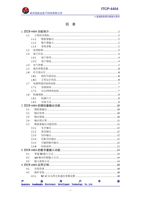
目录1. ITCP-4404功能简介 (1)1.1 主要技术指标 (2)1.1.1 模拟量输出 (2)1.1.2 数字量输入 (2)1.1.3 系统参数 (2)1.2 原理框图 (3)1.3 端子信息 (4)1.3.1 端子排列 (4)1.3.2 端子描述 (4)1.4 电气参数 (5)1.5 通信参数设置 (5)1.6 信号指示灯 (6)1.6.1 固件升级状态 (6)1.6.2 正常运行状态 (6)1.7 电源和通讯线的连接 (7)1.7.1 电源接线 (7)1.7.2 以太网网络连接 (7)1.8 机械规格 (8)1.8.1 机械尺寸 (8)1.8.2 安装方式 (8)2. ITCP-4404的模拟量输出功能 (10)2.1 模拟量输出 (10)2.2 输出原理 (10)2.3 输出接线 (10)2.4 输出值计算 (11)2.5 模拟量输出功能控制 (11)2.5.1 安全输出 (12)2.5.2 紧急输出 (12)2.5.3 同步输出 (12)2.5.4 匹配同步输出 (12)2.5.5 可编程顺序输出 (12)2.5.6 控制说明 (12)3. ITCP-4404的数字量输入功能 (14)3.1 普通DI输入方式 (14)3.2 AO输出匹配输入方式 (14)3.3 输入接线方式 (14)4. ITCP-4404应用示例 (16)4.1 安装设备 (16)4.2 操作设备 (16)4.2.1 RJ-45以太网主机通信参数设置 (16)4.2.2 模块信息配置 (17)4.2.3 功能操作 (19)5. ITCP-4404命令简析 (21)5.1 MODBUS/TCP协议命令结构 (21)5.2 MODBUS/TCP命令码介绍 (22)5.3 ITCP资源地址说明 (22)5.3.1 ITCP-4404的资源地址 (22)6. 免责声明 (23)1. ITCP-4404功能简介ITCP-4404是模拟量输出模块,可以同时输出4路的模拟量信号,内部采用12位分辩率DAC。
西门子440变频器参数的说明
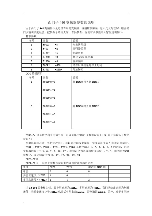
西门子440变频器参数的说明由于西门子440变频器不是电梯专用的变频器,调整比较麻烦,也不是太好理解。
结合我们以前调试的经验,把参数总结给大家,以供参考,现就有关参数给大家做说明如下:P700=2,这是数字命令的信号源,可以选择由键盘 (数值设为1)或 端子排输入(数字设为2)在电机自学习时,要把它改为1,可以通过面板来操作;完成后可改为2 实现正常运行。
P701 、P702、P703 、P704、P705、P706 是数字输入1、2、3、4、5、6的功能,对应变频器的端子号5、6、7、8、16、17 。
我们定义为多段速度选择位1、2、3、和使能BICO 参数化,即分别设定为17、17、17、99、99、99 P820=2835以1.6 m/s 的电梯为例,其单层速度为28HZ ,多层速度为45HZ 。
我们以给定速度为判断条件,当给定速度小于35HZ 时,激活单层曲线DDS0,否则激活DDS1。
另外,对于多层速度,我们对速度调节器的增益系数和积分时间常数做了一下切换,当实际速度小于7HZ时,激活DDS1,当实际速度大于7HZ时,激活DDS2,P2890=70%P2885=1024(r1024是实际的固定频率)P2885 是比较器1(说明书10-212页),当r1024大于或等于P2889时r2886=1; 当r1024小于P2889时r2886=0;要激活P2885 需要P2800=1 P2802[12]=1,比较的结果是r2886,我们把比较结果设在P2834(D—FF1即D-触发器1)中,P2834[0]=2886:0,置位P2834[1]=0:0,D-输入P2834[2]=0:0,存储脉冲P2834[3]=2813:0,复位D-触发器1有两个结果,r2835和r2836,而我们设定P820=2835,就选择DDS1。
而D-触发器1的激活级是P2801[12],故我们设定P2801[12]=3(优先级)而当P821=2811=1时,则选择DDS2,其中用到的参数有r53.2 p1080变频器的实际频率是否大于或等于P1080如果是则是1,如果不是则是0;其结果由p2828(NOT1)转换后由r2829 输出,p2801[9]是p2828的激活级;而r2829又和r2835通过p2812(AND2)与后由r2813输出结果,p2812p2801[1]又是p2812的激活级r2813r53.4p2155变频器的实际频率是否大于P2155如果是则是1,如果不是则是0,这个结果又通过p2810(AND1)由2811输出p2801[0]是2810的激活级r2811P2828=53:2P840=722:3=数字输入4,(要求P704 设定为99,BICO)正向运行的ON/OFF命令P842=722:4=数字输入5,(要求P705 设定为99,BICO)反向运行的ON/OFF命令这两个参数的社的设定只有在P719=0时才能激活。
- 1、下载文档前请自行甄别文档内容的完整性,平台不提供额外的编辑、内容补充、找答案等附加服务。
- 2、"仅部分预览"的文档,不可在线预览部分如存在完整性等问题,可反馈申请退款(可完整预览的文档不适用该条件!)。
- 3、如文档侵犯您的权益,请联系客服反馈,我们会尽快为您处理(人工客服工作时间:9:00-18:30)。
Symbol
Typ Max 374570100R θJL 2636Maximum Junction-to-Lead C
Steady-State
°C/W
Thermal Characteristics Parameter
Units Maximum Junction-to-Ambient A t ≤ 10s R θJA °C/W °C/W Maximum Junction-to-Ambient A Steady-State AO4404A
AO4404A
Symbol
Min Typ
Max
Units BV DSS 30
V 0.002
1T J =55°C
5I GSS 100nA V GS(th)0.71
1.5
V I D(ON)
40
A 1824T J =125°C
25302230m Ω3248
m Ωg FS 10
26S V SD 0.71
1V I S
4.5
A C iss 900
1100pF C oss 88pF C rss 65pF R g
0.95 1.5ΩQ g 10
12nC Q gs 1.8nC Q gd 3.75nC t D(on) 3.2
ns t r 3.5ns t D(off)21.5ns t f 2.7ns t rr 16.820ns Q rr
8
12nC
THIS PRODUCT HAS BEEN DESIGNED AND QUALIFIED FOR THE CONSUMER MARKET. APPLICATIONS OR USES AS CRITICAL COMPONENTS IN LIFE SUPPORT DEVICES OR SYSTEMS ARE NOT AUTHORIZED. AOS DOES NOT ASSUME ANY LIABILITY ARISING OUT OF SUCH APPLICATIONS OR USES OF ITS PRODUCTS. AOS RESERVES THE RIGHT TO IMPROVE PRODUCT DESIGN,FUNCTIONS AND RELIABILITY WITHOUT NOTICE.
Body Diode Reverse Recovery Time Body Diode Reverse Recovery Charge
I F =5A, dI/dt=100A/µs
Drain-Source Breakdown Voltage On state drain current
I D =250µA, V GS =0V V GS =2.5V, I D =5A
V GS =4.5V, V DS =5V V GS =10V, I D =8.5A
Reverse Transfer Capacitance Electrical Characteristics (T J =25°C unless otherwise noted)STATIC PARAMETERS Parameter
Conditions I DSS µA Gate Threshold Voltage V DS =V GS I D =250µA V DS =24V, V GS =0V
V DS =0V, V GS = ±12V Zero Gate Voltage Drain Current Gate-Body leakage current R DS(ON)
Static Drain-Source On-Resistance
Forward Transconductance
Diode Forward Voltage I F =5A, dI/dt=100A/µs V GS =0V, V DS =15V, f=1MHz SWITCHING PARAMETERS Total Gate Charge V GS =4.5V, V DS =15V, I D =8.5A
Gate Source Charge Gate Drain Charge Turn-On Rise Time Turn-Off DelayTime V GS =10V, V DS =15V, R L =1.8Ω, R GEN =6Ω
Turn-Off Fall Time
Maximum Body-Diode Continuous Current
Input Capacitance Output Capacitance Turn-On DelayTime DYNAMIC PARAMETERS Gate resistance
V GS =0V, V DS =0V, f=1MHz
m ΩV GS =4.5V, I D =8.5A I S =1A,V GS =0V V DS =5V, I D =5A
A: The value of R θJA is measured with the device mounted on 1in 2 FR-4 board with 2oz. Copper, in a still air environment with T A =25°C. The value in any given application depends on the user's specific board design. The current rating is based on the t ≤ 10s thermal resistance rating.B: Repetitive rating, pulse width limited by junction temperature.
C. The R θJA is the sum of the thermal impedence from junction to lead R θJL and lead to ambient.
D. The static characteristics in Figures 1 to 6 are obtained using 80 µs pulses, duty cycle 0.5% max.
E. These tests are performed with the device mounted on 1 in 2
FR-4 board with 2oz. Copper, in a still air environment with T A =25°C. The SOA curve provides a single pulse rating. Rev 0 : Jan 2006
AO4404A
AO4404A。
