LIC01-215H中文资料
CLS01资料
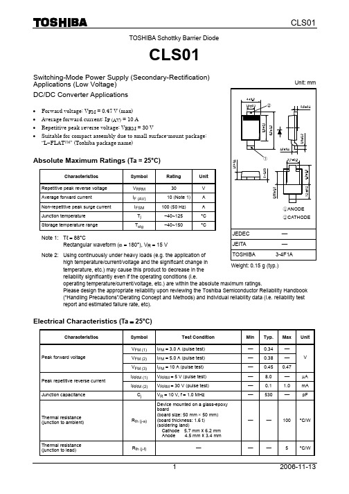
TOSHIBA Schottky Barrier DiodeCLS01Switching-Mode Power Supply (Secondary-Rectification)Applications (Low Voltage)DC/DC Converter Applications•Forward voltage: V FM = 0.47 V (max)•Average forward current: I F (AV) = 10 A•Repetitive peak reverse voltage: V RRM = 30 V•Suitable for compact assembly due to small surface-mount package:“L−FLAT TM” (Toshiba package name)Absolute Maximum Ratings (Ta = 25°C)Characteristics SymbolRatingUnitRepetitive peak reverse voltage V RRM30 VAverage forward current I F (AV)10 (Note 1) ANon-repetitive peak surge current I FSM100 (50 Hz) AJunction temperature T j−40~125 °CStorage temperature range T stg−40~150 °CNote 1: Tℓ= 88°CRectangular waveform (α= 180°), V R= 15 VNote 2: Using continuously under heavy loads (e.g. the application ofhigh temperature/current/voltage and the significant change intemperature, etc.) may cause this product to decrease in thereliability significantly even if the operating conditions (i.e.operating temperature/current/voltage, etc.) are within the absolute maximum ratings.Please design the appropriate reliability upon reviewing the Toshiba Semiconductor Reliability Handbook(“Handling Precautions”/Derating Concept and Methods) and individual reliability data (i.e. reliability testreport and estimated failure rate, etc).Electrical Characteristics (Ta = 25°C)Characteristics Symbol TestCondition MinTyp.Max UnitV FM (1)I FM= 3.0 A (pulse test) ⎯ 0.34 ⎯V FM (2)I FM= 5.0 A (pulse test) ⎯ 0.38 ⎯V Peak forward voltageV FM (3)I FM= 10 A (pulse test) ⎯ 0.45 0.47I RRM (1)V RRM= 5 V (pulse test) ⎯ 8.0 ⎯ μAPeak repetitive reverse currentI RRM (2)V RRM= 30 V (pulse test) ⎯ 0.1 1.0 mAJunction capacitance C j V R= 10 V, f = 1.0 MHz ⎯ 530 ⎯ pFThermal resistance (junction to ambient) R th (j-a)Device mounted on a glass-epoxyboard(board size: 50 mm × 50 mm)(board thickness: 1.6 t)(soldering land)Cathode 5.7 mm × 6.2 mmAnode 4.5 mm × 3.4 mm⎯ ⎯ 100°C/WThermal resistance (junction to lead) R th (j-ℓ)⎯ ⎯ ⎯ 5 °C/WUnit: mmWeight: 0.15 g (typ.)MarkingAbbreviation Code Part No.S01 CLS01Standard Soldering PadUnit: mmHandling Precautions1) Schottky barrier diodes have reverse current characteristics compared to other diodes. There is a possibilitythat SBDs will cause thermal runaway when used under high-temperature or high-voltage conditions. Be sure to take forward and reverse loss into consideration during design.2) The absolute maximum ratings denote the absolute maximum ratings, which are rated values that must not beexceeded during operation, even for an instant. The following are the general derating methods that we recommend for when designing a circuit incorporating this device.V RRM: Use this rating with reference to (1) above. V RRM has a temperature coefficient of 0.1%/°C. Take this temperature coefficient into account when designing a device for operation at lowtemperatures.I F (AV): We recommend that the worst case current be no greater than 80% of the absolute maximumrating of I F (AV) and that T j be below 100°C. When using this device, take the margin intoconsideration by using an allowable Tamax-I F (AV) curve.I FSM: This rating specifies the non-repetitive peak current. This applies only to abnormal operation,which seldom occurs during the lifespan of the device.T j: Derate this rating when using the device in order to ensure high reliability. We recommend that the device be used at a T j of below 100°C.3) Thermal resistance between junction and ambient fluctuates depending on the mounting condition of thedevice. When using the device, design the circuit board and soldering land size to match the appropriate thermal resistance value.4) Refer to the databook on Rectifiers for further information.0.00.20.40.60.8M a x i m u m a l l o w a b l e t e m p e r a t u r e T a m a x (°C )Instantaneous forward voltage v F (V)i F – v FI n s t a n t a n e o u s f o r w a r d c u r r e n t i F (A )Average forward current I F (AV) (A)P F (AV) – I F (AV)A v e r a g e f o r w a r d p o w e r d i s s i p a t i o n P F (A V ) (W )Average forward current I F (AV) (A)T ℓ max – I F (AV)M a x i m u m a l l o w a b l e l e a d t e m p e r a t u r e T ℓ m a x (°C )Average forward current I F (AV) (A)Ta max – I F (AV)4812167.00 4 8 164 0 8 16 12 120.0030.030.3330300T r a n s i e n t t h e r m a l i m p e d a n c e r t h (j -a ) (°C /W )Time t (s)r th (j-a) – tR e v e r s e c u r rentI R (m A )3 5 30 50A v e r a g e r e v e r s e p o w e rd i s si p a t i o nP R (A V) (W )Reverse voltage V R (V)C j – V R (typ.)J u n c ti o n ca pa c i t a n c e C j (p F )Number of cyclesSurge forward current(non-repetitive)P e a k s u r g e f or w a r d c u r r e nt I F S M(A )Junction temperature T j(°C)IR – T j(typ.)Reversevoltage V R(V)P R (AV) – V R (typ.)30 10 3 500 20 40 60 80 100 120 1601400 630181224RESTRICTIONS ON PRODUCT USE20070701-EN •The information contained herein is subject to change without notice.•TOSHIBA is continually working to improve the quality and reliability of its products. Nevertheless, semiconductor devices in general can malfunction or fail due to their inherent electrical sensitivity and vulnerability to physical stress. It is the responsibility of the buyer, when utilizing TOSHIBA products, to comply with the standards of safety in making a safe design for the entire system, and to avoid situations in which a malfunction or failure of such TOSHIBA products could cause loss of human life, bodily injury or damage to property.In developing your designs, please ensure that TOSHIBA products are used within specified operating ranges as set forth in the most recent TOSHIBA products specifications. Also, please keep in mind the precautions and conditions set forth in the “Handling Guide for Semiconductor Devices,” or “TOSHIBA Semiconductor Reliability Handbook” etc.• The TOSHIBA products listed in this document are intended for usage in general electronics applications (computer, personal equipment, office equipment, measuring equipment, industrial robotics, domestic appliances, etc.).These TOSHIBA products are neither intended nor warranted for usage in equipment that requires extraordinarily high quality and/or reliability or a malfunction or failure of which may cause loss of human life or bodily injury (“Unintended Usage”). Unintended Usage include atomic energy control instruments, airplane or spaceship instruments, transportation instruments, traffic signal instruments, combustion control instruments, medical instruments, all types of safety devices, etc.. Unintended Usage of TOSHIBA products listed in his document shall be made at the customer’s own risk.•The products described in this document shall not be used or embedded to any downstream products of which manufacture, use and/or sale are prohibited under any applicable laws and regulations.• The information contained herein is presented only as a guide for the applications of our products. No responsibility is assumed by TOSHIBA for any infringements of patents or other rights of the third parties which may result from its use. No license is granted by implication or otherwise under any patents or other rights of TOSHIBA or the third parties.• Please contact your sales representative for product-by-product details in this document regarding RoHS compatibility. Please use these products in this document in compliance with all applicable laws and regulations that regulate the inclusion or use of controlled substances. Toshiba assumes no liability for damage or losses occurring as a result of noncompliance with applicable laws and regulations.。
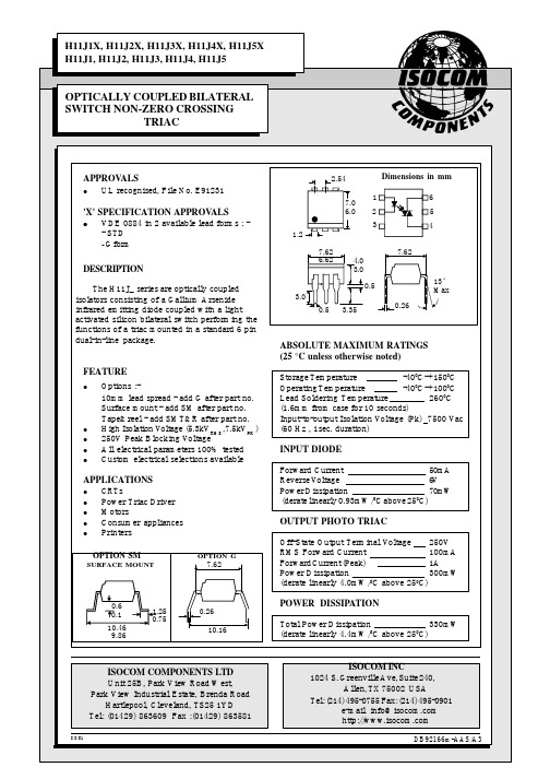
H11J2X中文资料
Output
Coupled
Input Current to Trigger ( IFT )(note 2 ) H11J1, H11J3 H11J2, H11J4 H11J5
10 15 25
mA mA mA
VD = 3V ( note 2 )
Holding Current , either direction ( IH ) Input to Output Isolation Voltage VISO 5300 7500
100
µA
VRMS VPK
See note 3 See note 3
Note 1. Test voltage must be applied within dv/dt rating. Note 2. Guaranteed to trigger at an IF value less than or equal to max. IFT , recommended IF lies between Rated IFT and absolute max. IFT . Note 3. Measured with input leads shorted together and output leads shorted together.
FEATURE l Options :10mm lead spread - add G after part no. Surface mount - add SM after part no. Tape&reel - add SMT&R after part no. l High Isolation Voltage (5.3kVRMS ,7.5kVPK ) l 250V Peak Blocking Voltage l All electrical parameters 100% tested l Custom electrical selections available APPLICATIONS l CRTs l Power Triac Driver l Motors l Consumer appliances l Printers
42115中文资料
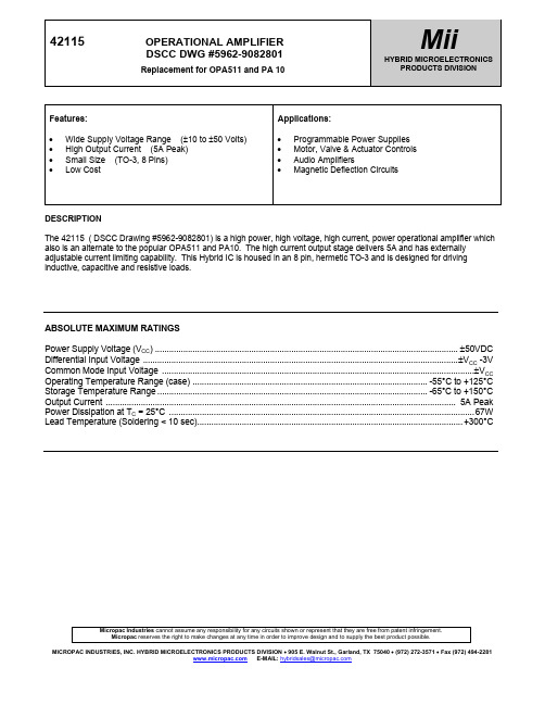
DIM INCHES
MILLIMETERS
MIN
MAX
MIN
MAX
A
1.510 1.550 38.35 39.37
B
0.760 0.780 19.30 19.81
C
0.290
7.37
D
0.97
1.07 0.038 0.042
E
0.080 0.100 2.03
2.54
F
40º BASIC
40º BASIC
Micropac Industries cannot assume any responsibility for any circuits shown or represent that they are free from patent infringement. Micropac reserves the right to make changes at any time in order to improve design and to supply the best product possible.
ABSOLUTE MAXIMUM RATINGS
Power Supply Voltage (VCC) ................................................................................................................................. ±50VDC Differential Input Voltage ......................................................................................................................................±VCC -3V Common Mode Input Voltage .....................................................................................................................................±VCC Operating Temperature Range (case) .................................................................................................... -55°C to +125°C Storage Temperature Range ................................................................................................................... -65°C to +150°C Output Current ..................................................................................................................................................... 5A Peak Power Dissipation at TC = 25°C ..................................................................................................................................67W Lead Temperature (Soldering < 10 sec)................................................................................................................. +300°C
1-215311-3资料
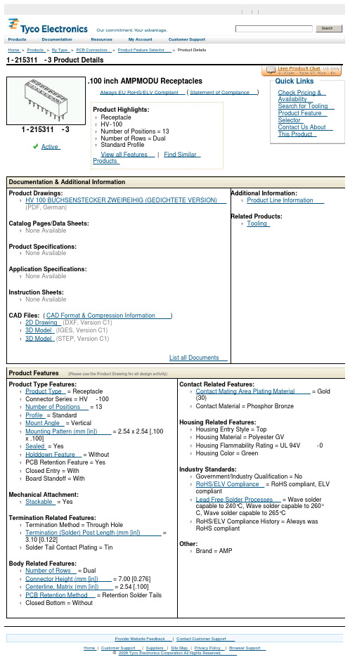
1-215311-3 Product DetailsHome | Customer Support | Suppliers | Site Map | Privacy Policy | Browser Support© 2008 Tyco Electronics Corporation All Rights Reserved SearchProducts Documentation Resources My Account Customer Support Home > Products > By Type > PCB Connectors > Product Feature Selector > Product Details1-215311-3Active .100 inch AMPMODU ReceptaclesAlways EU RoHS/ELV Compliant (Statement of Compliance)Product Highlights:?Receptacle?HV-100?Number of Positions = 13?Number of Rows = Dual?Standard ProfileView all Features | Find SimilarProductsCheck Pricing &AvailabilitySearch for ToolingProduct FeatureSelectorContact Us AboutThis ProductQuick LinksDocumentation & Additional InformationProduct Drawings:?HV 100 BUCHSENSTECKER ZWEIREIHIG (GEDICHTETE VERSION) (PDF, German)Catalog Pages/Data Sheets:?None AvailableProduct Specifications:?None AvailableApplication Specifications:?None AvailableInstruction Sheets:?None AvailableCAD Files: (CAD Format & Compression Information)?2D Drawing (DXF, Version C1)?3D Model (IGES, Version C1)?3D Model (STEP, Version C1)List all Documents Additional Information:?Product Line InformationRelated Products:?ToolingProduct Features (Please use the Product Drawing for all design activity)Product Type Features:?Product Type = Receptacle?Connector Series = HV-100?Number of Positions = 13?Profile = Standard?Mount Angle = Vertical?Mounting Pattern (mm [in]) = 2.54 x 2.54 [.100x .100]?Sealed = Yes?Holddown Feature = Without?PCB Retention Feature = Yes?Closed Entry = With?Board Standoff = WithMechanical Attachment:?Stackable = YesTermination Related Features:?Termination Method = Through Hole?Termination (Solder) Post Length (mm [in]) =3.10 [0.122]?Solder Tail Contact Plating = TinBody Related Features:?Number of Rows = Dual?Connector Height (mm [in]) = 7.00 [0.276]?Centerline, Matrix (mm [in]) = 2.54 [.100]?PCB Retention Method = Retention Solder Tails ?Closed Bottom = Without Contact Related Features:?Contact Mating Area Plating Material = Gold(30)?Contact Material = Phosphor BronzeHousing Related Features:?Housing Entry Style = Top?Housing Material = Polyester GV?Housing Flammability Rating = UL 94V-0?Housing Color = GreenIndustry Standards:?Government/Industry Qualification = No?RoHS/ELV Compliance = RoHS compliant, ELVcompliant?Lead Free Solder Processes = Wave soldercapable to 240°C, Wave solder capable to 260°C, Wave solder capable to 265°C?RoHS/ELV Compliance History = Always wasRoHS compliantOther:?Brand = AMPProvide Website Feedback | Contact Customer Support。
D200I资料
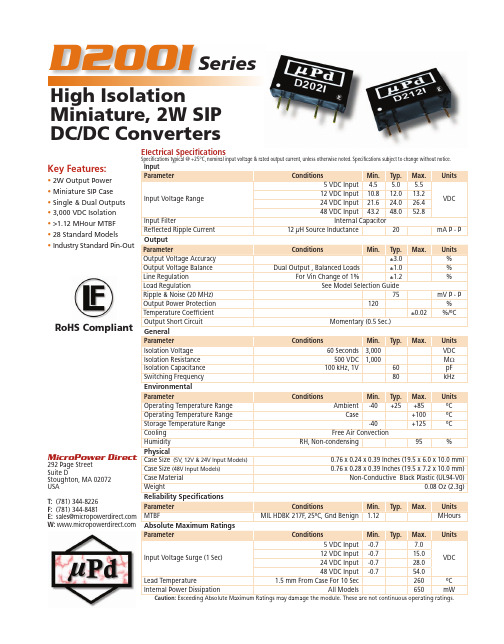
Key Features:• 2W Output Power • Miniature SIP Case • Single & Dual Outputs • 3,000 VDC Isolation • >1.12 MHour MTBF • 28 Standard Models •Industry Standard Pin-OutD200IHigh Isolation Miniature, 2W SIP DC/DC Con v ert ersSeriesMicroPower Direct292 Page Street Suite DStoughton, MA 02072USAT: (781) 344-8226F: (781) 344-8481E: sales@ W: RoHS CompliantElectrical Specifi cationsSpecifi cations typical @ +25°C, nominal input voltage & rated output current, unless otherwise noted. Specifi cations subject to change without notice.InputParameterConditions Min.Typ.Max.UnitsInput Voltage Range5 VDC Input 4.55.0 5.5VDC12 VDC Input 10.812.013.224 VDC Input 21.624.026.448 VDC Input 43.248.052.8Input Filter Internal CapacitorRefl ected Ripple Current12 μH Source Inductance 20mA P - POutputParameterConditionsMin.Typ.Max.Units Output Voltage Accuracy ±3.0%Output Voltage Balance Dual Output , Balanced Loads ±1.0%Line Regulation For Vin Change of 1%±1.2%Load RegulationSee Model Selection GuideRipple & Noise (20 MHz)75mV P - P Output Power Protection 120%Temperature Coeffi cient ±0.02%/ºCOutput Short CircuitMomentary (0.5 Sec.)GeneralParameterConditionsMin.Typ.Max.Units Isolation Voltage 60 Seconds 3,000VDC Isolation Resistance 500 VDC 1,000M ΩIsolation Capacitance 100 kHz, 1V60pF Switching Frequency80kHz EnvironmentalParameterConditionsMin.Typ.Max.Units Operating Temperature Range Ambient-40+25+85ºC Operating Temperature Range Case+100ºC Storage Temperature Range -40+125ºC Cooling Free Air ConvectionHumidityRH, Non-condensing95%PhysicalCase Size (5V, 12V & 24V Input Models)0.76 x 0.24 x 0.39 Inches (19.5 x 6.0 x 10.0 mm)Case Size (48V Input Models)0.76 x 0.28 x 0.39 Inches (19.5 x 7.2 x 10.0 mm)Case Material Non-Conductive Black Plastic (UL94-V0)Weight0.08 Oz (2.3g)Reliability Specifi cationsParameter ConditionsMin.Typ.Max.Units MTBFMIL HDBK 217F , 25ºC, Gnd Benign1.12MHours Absolute Maximum RatingsParameterConditionsMin.Typ.Max.UnitsInput Voltage Surge (1 Sec) 5 VDC Input -0.77.0VDC12 VDC Input -0.715.024 VDC Input -0.728.048 VDC Input-0.754.0Lead Temperature1.5 mm From Case For 10 Sec260ºC Internal Power Dissipation All Models650mWCaution: Exceeding Absolute Maximum Ratings may damage the module. These are not continuous operating ratings.Derating Curve• All dimensions are typical in inches (mm) Tolerance x.xx = ±0.01 (±0.25)Pin 1 is marked by a “dot” or indentation on the side of the unit Notes:1. Output load regulation is specifi ed for a load change of 20% to 100%.2. T hese units do not require external components to operate, but the use of an input ca-pacitor (10 μF) may enhance performance in some applications. It is recommended that an input capacitor of 4.7 u F to 47 u F (dependent upon the application) be used on 48V input model.An output capacitor (4.7 μF to 220 μF or ±4.7 μF to ±100 μF) may be used to reduce ripple. To improve EMI performance, a simple fi lter network consisting of a 10 u F to 100 u F capaci-tor and 12 u H inductor should be effective.3. These units will operate at no load without damage, but may not meet all specifi cations.4. D ual output units may be connected to provide a 10V, 24V or 30 VDC output. To do this, connect the load across the positive (+Vout) and negative (-Vout) outputs and fl oat the output common.5. It is recommended that a fuse be used on the input of a power supply for protection. See the table above for the correct rating.Other input/output combinations are available (i.e. 24.0 VDC). Contact the factory for details at:sales@Model Selection GuideMechanical DimensionsPin ConnectionsSingle Output (μF Max)Dual Output (μF Max)470±220Capacitive LoadModel Number InputOutput LoadRegulation (%, Max) Effi ciency(%, Typ)Fuse Rating Slow-Blow (mA)Voltage (VDC)Current (mA)Voltage (VDC)Current (mA, Max)Current(mA, Min)Nominal RangeFull-Load No-Load D201I 5 4.5 - 5.536730 3.3400.010.020721,000D202I 5 4.5 - 5.551230 5.0400.08.010781,000D203I 5 4.5 - 5.55003012.0165.0 3.510821,000D204I 5 4.5 - 5.55003015.0133.0 2.710821,000D205I 5 4.5 - 5.555530±5.0±200.0±4.010721,000D206I 5 4.5 - 5.551230±12.0±83.3±1.710781,000D207I 5 4.5 - 5.550030±15.0±66.6±1.410801,000D211I 1210.8 - 13.216920 3.3400.010.02065500D212I 1210.8 - 13.221620 5.0400.08.01077500D213I 1210.8 - 13.22032012.0165.0 3.51082500D214I 1210.8 - 13.22032015.0133.0 2.71082500D215I 1210.8 - 13.222220±5.0±200.0±4.01075500D216I 1210.8 - 13.220320±12.0±83.3±1.71082500D217I 1210.8 - 13.220320±15.0±66.6±1.41082500D221I 2421.6 - 26.47610 3.3400.010.02072200D222I 2421.6 - 26.410510 5.0400.08.01079200D223I 2421.6 - 26.41021012.0165.0 3.51080200D224I 2421.6 - 26.41011015.0133.0 2.71082200D225I 2421.6 - 26.411110±5.0±200.0±4.01075200D226I 2421.6 - 26.410110±12.0±83.3±1.71082200D227I 2421.6 - 26.410110±15.0±66.6±1.41082200D231I 4843.2 - 52.8456 3.3400.010.02060100D232I 4843.2 - 52.8546 5.0400.08.01077100D233I 4843.2 - 52.853612.0165.0 3.51078100D234I 4843.2 - 52.853615.0133.0 2.71078100D235I 4843.2 - 52.8576±5.0±200.0±4.01073100D236I 4843.2 - 52.8526±12.0±83.3±1.71080100D237I4843.2 - 52.8526±15.0±66.6±1.41080100Pin Single Dual 1+Vin +Vin 2-Vin -Vin 5-Vout -Vout 6No Pin Common 7+Vout+VoutNotes:All dimensio •Tolerance x •Pin 1 is maron the sideMicroPower Direct292 Page Street Ste D Stoughton, MA 02072 • TEL: (781) 344-8226 • FAX: (781) 344-8481 • E-Mail: sales@。
INA213AIDCKT中文资料

Reference Voltage
Supply
RSHUNT
Load
REF
GND
+2.7V to +26V
V+
CBYPASS 0.01mF
to
0.1mF
INA21x
OUT
R1
R3 IN-
Output
IN+
R2
R4
PRODUCT
INA210 INA211 INA212 INA213 INA214
GAIN
ELECTRICAL CHARACTERISTICS
Boldface limits apply over the specified temperature range, TA = –40°C to +125°C. At TA = +25°C, VSENSE = VIN+ – VIN–. INA210, INA213 and INA214: VS = +5V, VIN+ = 12V, VREF = VS/2, unless otherwise noted. INA211 and INA212: VS = +12V, VIN+ = 12V, VREF = VS/2, unless otherwise noted.
These devices operate from a single +2.7V to +26V power supply, drawing a maximum of 100µA of supply current. All versions are specified over the extended operating temperature range (–40°C to +125°C), and offered in an SC70 package.
15KE12CA中文资料
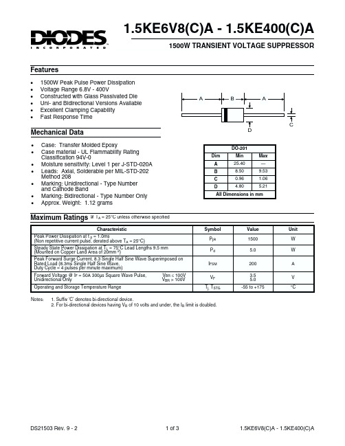
A
B
A
Mechanical Data
· · · · · · · Case: Transfer Molded Epoxy Case material - UL Flammability Rating Classification 94V-0 Moisture sensitivity: Level 1 per J-STD-020A Leads: Axial, Solderable per MIL-STD-202 Method 208 Marking: Unidirectional - Type Number and Cathode Band Marking: Bidirectional - Type Number Only Approx. Weight: 1.12 grams
1. Suffix ‘C’ denotes bi-directional device. 2. For bi-directional devices having VR of 10 volts and under, the IR limit is doubled.
DS21503 Rev. 9 - 2
VRWM, REVERSE STANDOFF VOLTAGE (V) Fig. 2 Typical Total Capacitance
DO-201 Dim A B C D Min 25.40 8.50 0.96 4.80
D
C
Max — 9.53 1.06 5.21
All Dimensions in mm
Maximum Ratings @ TA = 25°C unless otherwise specified
Characteristic Peak Power Dissipation at t p = 1.0ms (Non repetitive current pulse, derated above TA = 25°C) Steady State Power Dissipation at TL = 75°C Lead Lengths 9.5 mm (Mounted on Copper Land Area of 20mm 2) Peak Forward Surge Current, 8.3 Single Half Sine Wave Superimposed on Rated Load (8.3ms Single Half Sine Wave, Duty Cycle = 4 pulses per minute maximum) Forward Voltage @ IF = 50A 300µs Square Wave Pulse, Unidirectional Only Operating and Storage Temperature Range Notes: VBR £ 100V VBR > 100V Symbol Ppk Pd IFSM VF Tj, TSTG Value 1500 5.0 200 3.5 5.0 -55 to +175 Unit W W A V °C
EDR2H1B1200Z中文资料
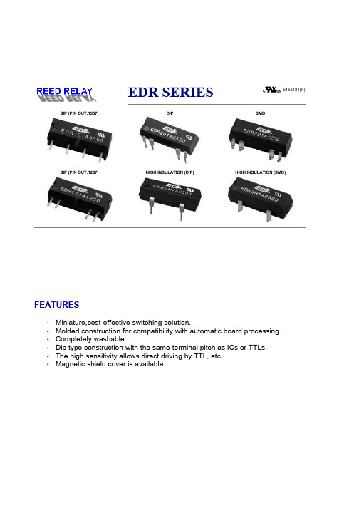
1400 VDC Min.
1400 VDC Min.
1400 VDC Min.
250 VDC Min. -40 ~ +85 -55 ~ +125 30G Min.
250 VDC Min. -40 ~ +85 -55 ~ +125 30G Min.
150 VDC Min. -40 ~ +85 -55 ~ +125 30G Min.
1A 2A 1B 1C
12 24 5 12 24 5 12 24 5 12 24
Special design are available on request.
CONTACT RATING Contact form
Switching current Carry current Switching power Electrical life Contact resistance Operate time (including bounce time) Release time Maximum voltage Insulation resistance (at 100 VDC) Coil to contact Across contacts Temperature range Operating temperature Storage temperature Shock resistance
1A
0.5 ADC Max. 1.0 ADC Max. 10 VA Max. (Ref 10VDC,10mA) 150m Max. 1x10⁸
2A
0.5 ADC Max. 1.0 ADC Max. 10 VA Max. (Ref 10VDC,10mA) 150m Max. 1x10⁸
F21CT1757(PT-0229C) 翻译
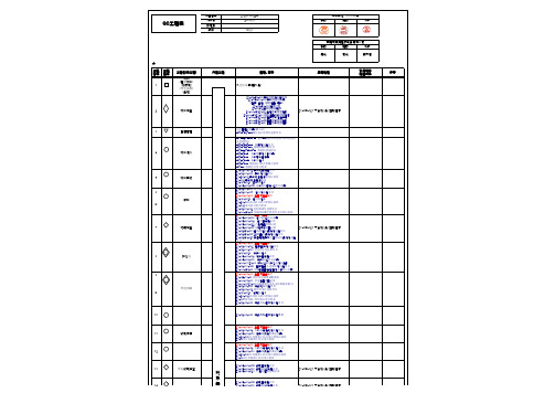
★:重要工程文書番号ZY20150122A 株式会社 リンク大洋作成日2015.6.3承認確認作成東莞市展揚硅胶制品有限公司承認確認作成改定日版数NO.1周光周光胡天海9★12ZY-link-YY-01 生産流程資料单ZY-WI-CC-002 硅胶自拆作业指导书ZY-WI-CC-003 手动冲压作业指导书ZY-GC-0026 冲拆标准卡ZY-QR-QC-014 冲拆首件确认单ZY-QR-QC-008 冲拆QC巡检记录表ZY-link-CCZY-03 PT-0229C 拆毛边作业指引ZY-WI-CC-005 硅胶産品毛边修理作业指导书ZY-link-PG-06 车载部品戴手指套作业点检记录表ZY-link-YY-01 生産流程資料单ZY-GF-YS-01 移印导电油墨调配规范ZY-link-YS-03 导电油墨调配记录ZY-link-YSZY-01 印刷油墨先进先出控制操作指引ZY-WI-YS-001 移印机操作指导书ZY-WI-YS-012 移印导电作业指导书ZY-GC-0026 印刷标准卡ZY-DJ-004 移印机日常点检图示说明ZY-007 移印机/丝印机日常点检表ZY-WI-YS-011 移印导电返修作业指导书ZY-WI-YS-011 移印导电返修作业指导书ZY-link-YY-01 生産流程資料单ZY-WI-YS-004 红外线烘烤机作业指导书ZY-QR-QC-010 烘干线条件检测记录表ZY-DJ-006 红外线烘干机日常点检图示说明ZY-011 红外线烘干机日常点检表ZY-QR-QC-015 印刷首件确认单ZY-QR-QC-009 印刷QC巡検确认单ZY-QR-QC-023 产品电阻值检测记录ZY-WI-YY-003 油压机操作指导书ZY-WI-YY-007 油压作业指导书ZY-link-YY-01 生産流程資料单ZY-GC-0026 油压标准卡ZY-DJ-003 油压机日常点检图示说明ZY-004 油压机日常点检表ZY-WI-YY-012 金粒排放作业指导书ZY-link-PG-06 车载部品戴手指套作业点检记录表ZY-link-YY-01 生産流程資料单ZY-QR-QC-006 油压QC巡检记录表ZY-QR-QC-004 油压首件确认单ZY-QR-QC-022 产品荷重检测记录ZY-QR-QC-007 每班尺寸测量记录ZY-WI-PG-033 曲线弹性仪操作作业指导书ZY-WI-PG-007 2D 测量仪操作作业指导书ZY-WI-PG-027 数字万用表及电阻测试仪操作作业指导书ZY-link-YYZY-03 备料RY硅胶原料摆放/领用先进先出管控指引ZY-WI-YY-005 炼胶作业指导书ZY-WI-YY-001 炼胶机操作指导书ZY-link-YYZY-01 炼胶机清洁指引ZY-PM-003 备料炼胶作业日报表ZY-PM-009 备料原料运行表ZY-GC-0026 备料标准卡ZY-DJ-001 炼胶机日常点检图示说明ZY-001 炼胶机日常点检表ZY-WI-YY-002 裁料机操作指导书ZY-WI-YY-006 裁料作业指导书ZY-DJ-002 裁料机日常点检图示说明ZY-002 裁料机日常点检表ZY-GC-0026 各料标准卡ZY-QR-QC-005 备料QC(首件)巡检记录表ZY-WI-PG-001来料检验作业指导书ZY-QR-QC-001来料检验记录表(硅胶、金粒、导电油墨、顔料)ZY-WI-PG-003抽样计划ZY-03-12抽样检验说明书ZY-link-PGZY-02 金粒进料检验指引ZY-link-PGZY-03 导电油墨进料检验指引ZY-link-PGZY-04 硅胶进料性能参照ZY-link-PGZY-05 硅胶进料检验指引ZY-link-PGZY-06 色膏进料检验指引仓库管理记录表(購入品)ZY-WI-PG-028颜色标示管理作业指导书ZY-link-YY-01 生産流程資料单ZY-WI-YS-004 红外线烘烤机作业指导书ZY-QR-QC-010 烘干线条件检测记录表ZY-DJ-006 红外线烘干机日常点检图示说明ZY-011 红外线烘干机日常点检表10引用規格関連文件外注工程記録、資料ZY-MP-021 不合格(品)控制程序入仓记录表(購入品)ZY-MP-021 不合格(品)控制程序ZY-MP-021 不合格(品)控制程序2QC工程表材料(硅胶材料)(加硫剤)(导电油墨)(金粒)工程番号1倉庫管理材料検査3工程名(本工程)工程記号54材料裁切材料混炼参考異常処理成形拆毛边117初期検査8导电印刷印刷干燥13导电印刷検査14ZY-MP-021 不合格(品)控制程序ZY-QR-QC-015 印刷首件确认单ZY-QR-QC-009 印刷QC巡検确认单6★対象無。
氯离子测定仪说明书

弘扬高科技企业之宗旨凭籍卓越质量品质迅速风靡煤质设备市场奉行低价位之经营策略遵循无限服务理念全面拓展煤质设备领域YXFL-6H氟氯离子测定仪使用说明书中国·河南市永心电子科技制造用心服务永心目录第一章简介01.1产品概述01.2测试原理11.3功能特点11.4技术参数1第二章结构组成与安装22.1仪器连接图示22.2设备安装步骤32.3安装注意事项4第三章试剂和材料的准备53.1试剂和材料5第四章仪器操作64.1控制面板介绍64.2显示界面介绍7第五章实验步骤操作85.1仪器准备85.2燃烧水解85.3电位测量9第六章结果计算106.1结果表达106.2方法的精密度11第七章常见故障及处理方法11第一章简介1.1产品概述氯是煤中的有害元素,煤在燃烧过程中,煤中氯大部分以氯化氢或有机氯化物等气态释放,对工业利用和环境污染具有直接或潜在的危害。
煤中氯含量也是评价煤炭品质主要指标之一。
因此,研究准确、快速检测煤中氯含量是十分必要的。
本实验设备采用高温燃烧水解法所得到氯离子样品溶液,以银为指示电极,银-氯化银为参比电极,用硝酸银电位法直接滴定冷凝液中的氯离子浓度,根据硝酸银标准溶液用量计算出煤中的氯含量,符合国标GB/T 3558-2014《煤中氯的测定方法》的要求。
1.2测试原理煤样和少量石英砂混合,在1100℃高温下与氧气和水蒸气混合气流中燃烧和水解,煤中氯全部转换为氯化物进入了冷凝水中并定量地溶于水中,以银为指示电极,银-氯化银为参比电极,用硝酸银电位法直接滴定冷凝液中的氯离子浓度,根据硝酸银标准溶液用量计算出煤中的氯含量。
1.3功能特点●采用中文液晶显示,界面友好,操作简单。
●采用PID控制炉流,控温精度高,有效延长硅碳管使用寿命。
●测温采用高精度、低温漂元器件,保证了测温的长期准确性。
●支持定时送样提醒功能。
●支持故障自诊断功能,超温保护功能。
●蒸发量调节电位器采用TOCOS电位器,线性度高,使用寿命长。
普通CL电磁流量计(一级菜单)说明书
电磁流量计转换器使用说明书V2.4目录一. 产品功能说明 (3)1、基本功能 (3)2、正常工作条件 (3)3、与传感器连接型式 (3)4、安装尺寸图 (3)4.1.一体型转换器(HKR-T1) (3)4.2.一体型转换器(HKR-T2) (4)4.3.一体型转换器(HKR-T3) (4)4.4.分体型转换器(HKR-T-F) (5)二. 技术性能指标 (6)2.1执行标准 (6)2.2基本参数与性能指标 (6)2.2.1配套传感器公称通径(mm) (6)2.2.2传感器配套要求 (6)2.2.4电流输出 (6)2.2.5频率输出 (6)2.2.6脉冲输出 (7)2.2.7报警输出 (7)2.2.8数字通讯接口及通讯协议 (7)三. 转换器操作和参数设置 (7)3.1键盘定义与显示 (7)3.2转换器主界面说明 (7)3.3转换器菜单和参数说明 (8)3.3.1转换器菜单结构及其相关说明 (8)3.4参数设置及操作 (10)3.4.1通用操作 (10)3.4.2仪表校准 (11)四、转换器 (11)4.1HKR一体型转换器端子接线图 (11)4.2HKR分体型转换器列端子接线 (12)4.3信号线和励磁线接线 (14)5.1数字量输出及计算 (14)5.1.1频率输出: (14)5.1.2脉冲输出方式: (14)5.2模拟量输出及计算 (15)六、报警信息 (15)五、使用HKR转换器的流量计校验注意事项 (15)6.1正确安装 (15)6.2充分预热 (16)6.3正确设置仪表参数 (16)6.4校验零点 (16)6.5空满管校准 (16)六、故障处理 (17)7.1显示屏黑屏 (17)7.2显示屏亮却无任何字符 (17)7.3励磁报警,无流量 (17)7.4空管报警,无流量 (17)7.5实际流量稳定,而测量流量波动大 (17)7.6实际流量为零,而流量计不回零 (17)7.7流量偏小 (18)7.8流量偏大 (18)八HKR装箱与贮存 (18)8.1HKR装箱 (18)8.2运输和贮存 (18)九、附录“RS485通讯地址表” (19)1、仪表变量地址定义 (19)2、附录2:常用单位定义 (20)九. 附录(RS485通讯) (25)1、仪表变量地址定义(附录1) (25)2、常用单位定义(附录2) (26)一. 产品功能说明1.1基本功能■励磁方式:矩形波励磁■励磁频率:25HZ(适用于测浆液)、12.5HZ、6.25HZ、3.125HZ;■励磁电流可选定为160mA、250mA■空管测量功能,连续测量,定值报警;■流速测量范围:0.1 --- 15米/秒,流速分辨率:0.5毫米/秒;■交流高频开关电源,电压适用范围:85V AC --- 265V AC;■直流24V开关电源,电压适用范围:18VDC --- 36VDC;■通讯功能:RS485(MODBUS)、MBmagCPV4.2;■中文、英文,液晶显示方式;■内部有三个积算器总量,可分别记录:正向总量、反向总量、差值总量。
- 1、下载文档前请自行甄别文档内容的完整性,平台不提供额外的编辑、内容补充、找答案等附加服务。
- 2、"仅部分预览"的文档,不可在线预览部分如存在完整性等问题,可反馈申请退款(可完整预览的文档不适用该条件!)。
- 3、如文档侵犯您的权益,请联系客服反馈,我们会尽快为您处理(人工客服工作时间:9:00-18:30)。
1/6
Application Specific Discretes
A.S.D.™
September 2000-Ed:7B LIGHT IGNITION CIRCUIT
The LIC01has been especially designed for high voltage pulse generation circuits such as light ignitors for :
.High pressure sodium lamp .Lamp flashing circuit .Metal Halid lamp
It uses a high performance planar diffused technol-ogy device suitable for high surge current opera-tion in rugged environmental conditions.
When the voltage across the device reaches the breakover voltage,it decreases from an off-state to low voltage on-state condition.When the current through the circuit drops below the holding current I H ,the device comes back to the off-state.
DESCRIPTION
FUNCTIONAL DIAGRAM
DEVICE TYPE BREAKDOWN VOLTAGE
RANGE LIC01-195V BO min:195V V BO max:230V LIC01-215
V BO min:215V V BO max:255V
TECHNOLOGY
LIC01 Series
2/6
Symbol Parameter
Value Unit Rth(j-a)Junction to ambient 100°C/W Rth(j-c)
Junction to case
3.5
°C/W
THERMAL RESISTANCE
ORDERING INFORMATION
Symbol Parameter
Value Unit I TRM Repetitive surge peak on state current tp =10µs (note 1)
±50A I T(RMS)RMS on state current
T amb =90°C
1.2A di/dt Critical rate of rise on state current 80A/µs V DRM /V RRM
Repetitive peak off state voltage Tj =125°C 180V Tstg Storage junction temperature range -40to +125°C Tj Operating junction temperature range
-20to 125°C T L
Maximum lead temperature for soldering during 10s
260
°C
Note 1:Test current waveform
ABSOLUTE RATINGS (limiting values)
LIC01 Series
3/6
Symbol Parameters
V RM Stand-off voltage V TM On-state voltage V BO Breakover voltage I TM On-state current I H Holding current I BO Breakover current I RM
Leakage current
ELECTRICAL CHARACTERISTICS Symbol Test conditions
Value Unit I RM V D =V RM 180V Tj =25°C MAX 5µA Tj =125°C MAX 50µA V BO
I BO
LIC01-195Tj =25°C MIN 195V
MAX 230LIC01-215
Tj =25°C MIN 215V MAX 255I BO V BO max.Tj =25°C TYP 200µA MAX 500I H I T =350mA Tj =25°C MIN 50mA V TM
I TM =1A
Tj =25°C
MAX
5
V ELECTRICAL PARAMETERS IT
0.1A/div
IH -
IH +
t =
2ms/div
Auxiliary network providing the complete HOLDING CURRENT TEST CIRCUIT
LIC01 Series
4/6
VARIATION OF V BO VERSUS JUNCTION TEMPERATURE
TYPICAL APPLICATION
When the peak voltage across C1reaches the break over voltage VBO of the LIC01,this device turns on and produces a pulse of current through the primary of the transformer.In turn,the trans-former generates high voltage pulses across the
lamp.
VARIATION OF V BO VERSUS JUNCTION
TEMPERATURE
LIC01 Series
5/6
PACKAGE MECHANICAL DATA DPAK (Plastic)
FOOT PRINT DIMENSIONS (in millimeters)
LIC01 Series
6/6
Information furnished is believed to be accurate and reliable.However,STMicroelectronics assumes no responsibility for the consequences of use of such information nor for any infringement of patents or other rights of third parties which may result from its use.No license is granted by implication or otherwise under any patent or patent rights of STMicroelectronics.Specifications mentioned in this publication are subject to change without notice.This publication supersedes and replaces all information previously supplied.
STMicroelectronics products are not authorized for use as critical components in life support devices or systems without express written ap-proval of STMicroelectronics.
The ST logo is a registered trademark of STMicroelectronics ©2000STMicroelectronics -Printed in Italy -All rights reserved.
STMicroelectronics GROUP OF COMPANIES
Australia -Brazil -China -Finland -France -Germany -Hong Kong -India -Italy -Japan -Malaysia
Malta -Morocco -Singapore -Spain -Sweden -Switzerland -United Kingdom -U.S.A.
PACKAGE MECHANICAL DATA
Type Marking Package Weight Base qty
Delivery mode
LIC01-xxxH LIC01-xxxH IPAK 0.4g 75Tube LIC01-xxxB
LIC01-xxxB
DPAK
0.3g
75
Tube
OTHER INFORMATION。
