CCF-5539K2FKE36中文资料
Secure Series II 产品说明书
This document provides firmware update instructions and describes what is new in this firmware version for the SUHD553-L, SUHD653-L, SUHD753-L, SUHD863-L.This is the initial release for the Secure Series II panels (SUHD553-L, SUHD653-L, SUHD753-L, SUHD863-L) for the Scaler firmware v1.0.1.8 and Ethernet firmware v14.Follow these steps to update the scaler firmware.Learn how to update the scaler firmware.Christie recommends updating the scaler firmware using the USB method as it is faster than the webserver update method.1.Upload the firmware for the A/D board.2.Plug in a USB memory to the service terminal.3.Enter the Factory-Menu.To enter the Factory-Menu by remote control:After version 1.0.2.1-114.5.Select USB Update.For compatible USB storage devices a Connected message appears. Proceed to step 5. If the USB storage device is not compatible, proceed to step 6.6.If Connected appears, select USB Update.The firmware is updated automatically and the panel goes into Standby mode after a successfulfirmware update (about 30 seconds).a.Reset the main power switch to turn the panel back on.b.When the firmware update is complete, From the Factory-Menu perform an Initial Setting.c.After Initial Setting, power off the panel using the rocker-switch.d.Wait at least 10 seconds and power the panel back on.7.If the USB storage device is not compatible, a Not Connected USB message appears.8.For the software version to upload correctly, ensure the filename is SUHD983P.bin.Follow these steps to update the Ethernet firmware.1.To use a static IP address, select Disable under DHCP.•The default static IP address is 192.168.10.10.•At initial power on, it may take up to 30 seconds for the IP address to be active.2.Select DHCP Enable to use a dynamic IP address.•If there is router, the IP address starts with 192.166.•If there is no router, the IP address starts with 169.254.1.Go to Local Network Setting > Internet protocol version 4 (TCP/IPv4).2.If DHCP is disabled, set the IP address and Subnet mask.The IP address must be a different address than the display.IP address : 192.168.10.50Subnet Mask : 255.255.255.03.If DHCP is enabled, select Obtain an IP address automatically.The ping test checks the Ethernet connection.1.Press Windows + R.2.Type cmd and click OK.3.Type ping –t 192.168.10.10.4.Replace the IP address with the address of the display panel.A response similar to below indicates the ping test was successful.A response similar to below indicates the ping test failed.Connect to the built-in web server open a Web browser (for example, Internet Explorer, Chrome) and follow the instructions below.1.In a web browser, go to the address of the display panel.The web page provides all menu controls on the on-screen display.2.To set a value, click Apply.3.To display the current value, click Read.4.To upgrade the Ethernet or Scaler firmware, go to the General settings page.•Ethernet firmware update time: approximately 5 minutes.File name : Ethernet_FW_Secure_Series_II_V*.bin•Scaler firmware update time: approximately 8 minutesSecure_Series_II.binIf you updated the scaler firmware using the USB method, it does not need to be updated again inthe web server.Before staring the updates, ensure the following settings are selected in the Setup menu of the WebUI or the on screen display:•Setup > Power Save > Off•Setup > Power Off Mode > StandbyScaler F/W update:The panel turns off approximately three minutes after the update starts. Once the update is complete (takes approximately five to eight minutes) an Update completed. Please reboot. messageappears on the WebUI and the panel powers on.Ethernet F/W update:The panel stays on throughout the update. Once the update is complete (takes approximately five to eight minutes) an Update completed. Please reboot. message appears on the WebUI and thepanel stays on.5.Power off the unit using the remote control.6.Power cycle the panel by turning the rocker switch to the OFF position and back to ON after 15 seconds.7.Power on the panel.8.To confirm version of the firmware, click the About page on the WebUI or the panel on-screen display. For installation, setup, and user information, see the product documentation available on the Christiewebsite. Read all instructions before using or servicing this product.1.Access the documentation from the Christie website:•Go to this URL: https://bit.ly/2VccFTr orhttps:///products/lcd-panels/secure-series-II/•Scan the QR code using a QR code reader app on a smartphone or tablet.2.On the product page, select the model and switch to the Downloads tab.Additional information on the LCD panels is available in the following documents.•Secure Series II LCD Panels Product Safety Guide (P/N: 020-001778-XX)•Secure Series II LCD Display Panels External Commands (P/N: 020-001915-XX)•SUHD553-L LCD Panels Service Guide (P/N: 020-001850-XX)•SUHD653-L LCD Panels Service Guide (P/N: 020-001851-XX)•SUHD753-L LCD Panels Service Guide (P/N: 020-001876-XX)•SUHD863-L LCD Panels Service Guide (P/N:020-001877-XX)Technical support for Christie products is available at:•North and South America: +1-800-221-8025 or ************************************•Europe, Middle East, and Africa: +44 (0) 1189 778111 or ********************************•Asia Pacific•Australia: +61 (0)7 3624 4888•China: +86 10 6561 0240•India: +91 (80) 6708 9999•Japan: 81-3-3599-7481•Singapore: +65 6877-8737•South Korea: +82 2 702 1601•Christie Professional Services: +1-800-550-3061 or ***********************。
S553-6500-61中文资料
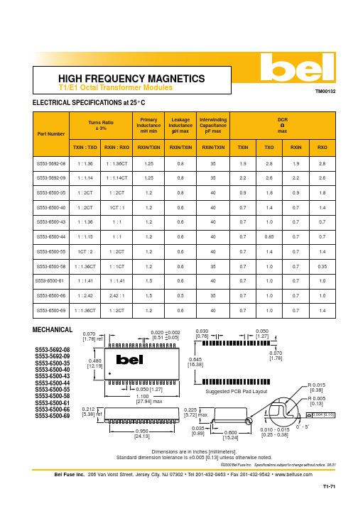
©2000 Bel Fuse Inc. Specifications subject to change without notice. 06.01ELECTRICAL SPECIFICATIONS at 25° CMECHANICALDimensions are in inches [millimeters].Standard dimension tolerance is ±0.005 [0.13] unless otherwise noted.S553-5692-08S553-5692-09S553-6500-35S553-6500-40S553-6500-43S553-6500-44S553-6500-55S553-6500-58S553-6500-61S553-6500-66S553-6500-69©2000 Bel Fuse Inc. Specifications subject to change without notice. 06.01SCHEMATICSS553-5692-08S553-5692-09S553-6500-35123467891112131416171819403938353433302928252423510152021263136RXO-RXOCT RXO+TXIN+TXIN-RXO-RXOCT RXO+RXO-TXIN+TXIN-RXOCT RXO+RXO-TXIN+TXIN-RXO+RXOCT TXIN+TXIN-RXIN-RXIN+TXO+RXIN-RXIN+RXIN-TXO+TXO-RXIN+RXIN-TXO+TXO-RXIN+TXO+TXO-TXO-1234678912131416171819403938353433302928252423510152021263136RXO-RXOCT RXO+TXIN+TXIN-RXO-RXOCT RXO+RXO-TXIN+TXIN-RXOCT RXO+RXO-TXIN+TXIN-RXO+RXOCT TXIN+TXIN-RXIN-RXIN+TXO+RXIN-RXIN+RXIN-TXO+TXO-RXIN+RXIN-TXO+TXO-RXIN+TXO+TXO-TXO-1234567891012131415161718192040RXO+RXOCT RXO-TXIN+TXIN-RXO+RXOCT RXO-TXIN+TXIN-RXO+RXOCT RXO-TXIN-TXIN+TXIN-TXIN+RXO-RXO+RXOCT TXO-TXOCT TXO-TXO-TXO-TXO+TXO+TXO+TXO+TXOCT TXOCTTXOCT RXIN+RXIN+RXIN+RXIN+RXIN-RXIN-RXIN-RXIN-S553-6500-401234567891011121314151617181920RXIN-RXINCT RXIN+TXIN+TXIN-RXIN-RXINCT RXIN+RXIN-TXIN+TXIN-RXINCT RXIN+RXIN-TXIN+TXIN-RXIN+RXINCT TXIN+TXIN-4039383736353433323130292827212223242526RXO-TXOCT RXO+TXO+TXO-RXO-TXOCT RXO+RXO-TXO+TXO-TXOCT RXO+RXO-TXO+TXO-RXO+TXOCT TXO+TXO-©2000 Bel Fuse Inc. Specifications subject to change without notice. 06.01SCHEMATICSS553-6500-43S553-6500-44S553-6500-581345689101113141516181920RXO-RXO+TXIN-TXIN+RXO-RXO+TXIN-TXIN+RXO-RXO+TXIN-TXIN+RXO-RXO+TXIN-TXIN+40383736353332313028272625232221RXIN-RXIN+TXO-TXO+RXIN-RXIN+TXO-TXO+RXIN-RXIN+TXO-TXO+RXIN-RXIN+TXO-TXO+1345689101113141516181920RXO-RXO+TXIN-TXIN+RXO-RXO+TXIN-TXIN+RXO-RXO+TXIN-TXIN+RXO-RXO+TXIN-TXIN+40383736353332313028272625232221RXIN-RXIN+TXO-TXO+RXIN-RXIN+TXO-TXO+RXIN-RXIN+TXO-TXO+RXIN-RXIN+TXO-TXO+123467891112131416171819RXO-RXO+TXIN-TXIN+RXO-RXO+TXIN-TXIN+RXO-RXO+TXIN-TXIN+RXO-RXO+TXIN-TXIN+RXIN-RXIN+TXO-TXO+40393837353433323029282725242322RXIN-RXIN+TXO-TXO+RXIN-RXIN+TXO-TXO+RXIN-RXIN+TXO-TXO+510152021263136TXOCT TXOCT TXOCT TXOCT RXOCT RXOCT RXOCT RXOCT S553-6500-551234567891012131415161718192040TXO+TXINCT TXO-RXIN+RXIN-TXO+TXINCT TXO-TXIN+RXIN-TXO+TXINCT TXO-RXIN+RXIN+RXO-RXO+TXO-TXO+TXINCT RXIN-RXINCT RXIN-RXIN+RXINCTRINCTRXINCT RXO+TXIN+TXIN+TXIN+TXIN-TXIN-TXIN-TXIN-RXO+RXO-RXO-RXO-RXO+CORPORATEBel Fuse Inc.206 Van Vorst Street Jersey City, NJ 07302T el 201-432-0463FAR EASTBel Fuse Ltd.8F / 8 Luk Hop Street San Po KongKowloon, Hong Kong EUROPEBel Fuse Europe Ltd.Preston T echnology Management Centre Marsh Lane, Suite G7, Preston Lancashire, PR1 8UD, U.K.©2000 Bel Fuse Inc. Specifications subject to change without notice. 06.01S553-6500-61SCHEMATICSS553-6500-66S553-6500-691234678912131416171819RXO-RXO+TXIN-TXIN+RXO-RXO+TXIN-TXIN+RXO-RXO+TXIN-TXIN+RXO-RXO+TXIN-TXIN+RXIN-RXIN+TXO-TXO+40393837353433323029282725242322RXIN-RXIN+TXO-TXO+RXIN-RXIN+TXO-TXO+RXIN-RXIN+TXO-TXO+123467891112131416171819RXO-RXO+TXIN-TXIN+RXO-RXO+TXIN-TXIN+RXO-RXO+TXIN-TXIN+RXO-RXO+TXIN-TXIN+RXIN-RXIN+TXO-TXO+40393837353433323029282725242322RXIN-RXIN+TXO-TXO+RXIN-RXIN+TXO-TXO+RXIN-RXIN+TXO-TXO+1234678912131416171819RXO-RXO+TXIN-TXIN+RXO-RXO+TXIN-TXIN+RXO-RXO+TXIN-TXIN+RXO-RXO+TXIN-TXIN+RXIN-RXIN+TXO-TXO+40393837353433323029282725242322RXIN-RXIN+TXO-TXO+RXIN-RXIN+TXO-TXO+RXIN-RXIN+TXO-TXO+510152021263136TXOCT TXOCT TXOCT TXOCT RXOCT RXOCT RXOCT RXOCT •Octal transformer solutions for T1/E1 applications including concentrators, channel banks and cellular base stations•Octals utilize Bel’s popular 40-pin SMD package •Designed to meet the stringent demands of high density designs•Minimum interwinding breakdown voltage of 1500 Vrms •Designed for UL1459/UL1950•For operating temperature range of -40° to +85° C,OCL is 600µH minimum at -40° C。
AD5539资料
One Technology Way, P.O. Box 9106, Norwood, MA 02062-9106, U.S.A. Tel: 617/329-4700 Fax: 617/326-8703
AD5539–SPECIFICATIONS (@ +25؇C and V = ؎8 V dc, unless otherwise noted)
S
Parameter INPUT OFFSET VOLTAGE Initial Offset1 TMIN to TMAX INPUT OFFSET CURRENT Initial Offset2 TMIN to TMAX INPUT BIAS CURRENT Initial2 VCM = 0 Either Input TMIN to TMAX FREQUENCY RESPONSE RL = 150 Ω3 Small Signal Bandwidth ACL = 24 Gain Bandwidth Product ACL = 26 dB Full Power Response ACL = 24 ACL = 7 ACL = 20 Settling Time (1%) Slew Rate Large Signal Propagation Delay Total Harmonic Distortion RL = ∞ RL = 100 Ω3 VOUT = 2 V p–p ACL = 7, f = 1 kHz INPUT IMPEDANCE OUTPUT IMPEDANCE (f <10 MHz) INPUT VOLTAGE RANGE Differential5 (Max Nondestructive) Common-Mode Voltage (Max Nondestructive) Common-Mode Rejection Ratio ∆VCM = 1.7 V RS = 100 Ω TMIN to TMAX INPUT VOLTAGE NOISE Wideband RMS Noise (RTI) BW = 5 MHz; RS = 50 Ω Spot Noise F = 1 kHz; RS = 50 Ω OPEN-LOOP GAIN VO = +2.3 V, –1.7 V RL = 150 Ω3 RL = 2 kΩ TMIN to TMAX –RL = 2 kΩ
ioLogik设备说明书
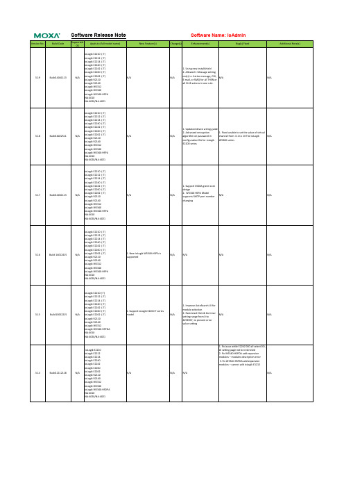
ioLogik W5340
ioLogik W5340-HSPA
NA-4010
NA-4020/NA-4021
Change(s)
Software Name: ioAdmin
Enhancement(s)
Bug(s) Fixed
Additional Note(s)
1. Using new installshield
E2200 series
1. Support MOXA green core
design
N/A
2. W5340-HSPA Model supports SMTP port number
N/A
N/A
changing
ioLogik E2210 (-T)
ioLogik E2212 (-T)
ioLogik E2214 (-T)
N/A
ioLogik E2262 (-T) ioLogik R2110
N/A
ioLogik R2140
ioLogik W5312
ioLogik W5340
ioLogik W5340-HSPA
NA-4010
NA-4020/NA-4021
ioLogik E2210 (-T)
ioLogik E2212 (-T)
NA-4020/NA-4021
New Feature(s)
ioLogik E2210 (-T)
ioLogik E2212 (-T)
ioLogik E2214 (-T)
ioLogik E2240 (-T)
ioLogik E2242 (-T)
ioLogik E2260 (-T)
3.18
Build16022511
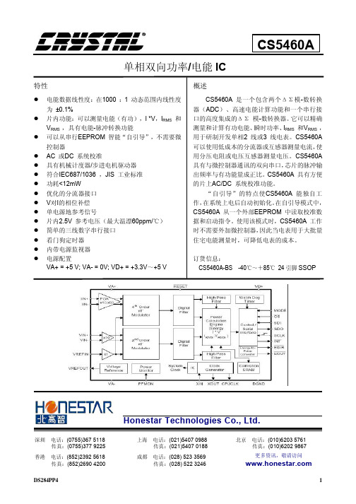
CS5463A中文资料手册pdf
CS5339-KP资料
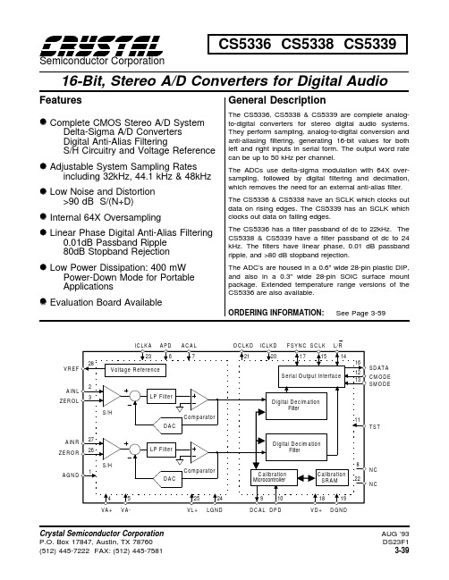
Features•Complete CMOS Stereo A/D System Delta-Sigma A/D Converters Digital Anti-Alias FilteringS/H Circuitry and Voltage Reference •Adjustable System Sampling Rates including 32kHz, 44.1 kHz & 48kHz•Low Noise and Distortion>90 dB S/(N+D)•Internal 64X Oversampling•Linear Phase Digital Anti-Alias Filtering0.01dB Passband Ripple 80dB Stopband Rejection•Low Power Dissipation: 400 mW Power-Down Mode for Portable Applications•Evaluation Board AvailableGeneral DescriptionThe CS5336, CS5338 & CS5339 are complete analog-to-digital converters for stereo digital audio systems.They perform sampling, analog-to-digital conversion and anti-aliasing filtering, generating 16-bit values for both left and right inputs in serial form. The output word rate can be up to 50 kHz per channel.The ADCs use delta-sigma modulation with 64X over-sampling, followed by digital filtering and decimation,which removes the need for an external anti-alias filter.The CS5336 & CS5338 have an SCLK which clocks out data on rising edges. The CS5339 has an SCLK which clocks out data on falling edges.The CS5336 has a filter passband of dc to 22kHz. The CS5338 & CS5339 have a filter passband of dc to 24kHz. The filters have linear phase, 0.01 dB passband ripple, and >80 dB stopband rejection.The ADC’s are housed in a 0.6" wide 28-pin plastic DIP,and also in a 0.3" wide 28-pin SOIC surface mount package. Extended temperature range versions of the CS5336 are also available.ORDERING INFORMATION: See Page 3-59Crystal Semiconductor Corporation AUG ’9316-Bit, Stereo A/D Converters for Digital AudioSemiconductor CorporationA IN R S /HA G N DD A CA IN L S /HD A CS erial O utput InterfaceVoltage R eferenceV R E FC alibration S R A M C om paratorC om paratorLP FilterLP FilterZER O LZ ER O R272623128V D +18D G N D1917V A -5V L +25V A +4S M O D E13N C22N C 8T S T11S C LK15A P D6A C A L7IC LK A23D P D10D C A L 9LG N D24D igital D ecim ationFilterD igital D ecim ationFilterC alibration Microcontroller L/R 14F SYN C S D A T A 16CM O D E 12IC LK D20O C LK D21CS5336 CS5338 CS5339CS5336,8,9-K CS5336-B CS5336-TParameterSymbol Min Typ Max Min Typ Max Min Typ Max Units Specified Temperature Range T A0to 70-40to +85-55to +125°C Resolution16--16--16--Bits Dynamic PerformanceDynamic Range92.795.7-9093.5-8492-dB Signal-to-(Noise + Distortion); THD+N S/(N+D)90.792.7-8589-8286-dB Signal to Peak Noise -96--95--94-dB Total Harmonic Distortion THD.0025.001-.005.001-.013.005-%Interchannel Phase Deviation -.0001--.0001--.0001-°Interchannel Isolation (dc to 20 kHz)100106-90106-8396-dB dc AccuracyInterchannel Gain Mismatch -0.010.05-.01.05-.010.1dB Gain Error (includes Vref tolerance)-±1±5-±2±5-±3±6%Gain Drift (includes Vref drift, Note 1)-25--70--70-ppm/°C Bipolar Offset Error (Note 2)-±5±15-±10±30-±16±65LSB Offset Drift (Note1)-15--20--20-ppm/°C ANALOG CHARACTERISTICS (Logic 0 = GND; Logic 1 = VD+; K grade: T A = 25°C; B and Tgrades: T A = T MIN to T MAX ; VA+, VL+,VD+ = 5V; VA- = -5V; Full-Scale Input Sinewave, 1kHz; Output word rate = 48 kHz; SCLK = 3.072 MHz; Source Impedance = 50Ω with 10 nF to AGND; Measurement Bandwidth is 10 Hz to 20 kHz; unless otherwise specified.)Analog Input Input Voltage Range (±Full Scale)VIN ±3.5 ±3.68-±-3.5±3.68-±3.5±3.68-V Input ImpedanceZIN-65--65--65-k ΩPower SuppliesPower Supply Current (VA+)+(VL+)IA+-2535-2535-2535mA with APD, DPD low VA-IA---25-35--25-35--25-35mA (Normal Operation)VD+ID+-3045-3045-3050mA Power Supply Current (VA+)+(VL+)IA+-1050-1050-1050µA with APD, DPD high VA-IA---10-50--10-50--10-50µA (Power-Down Mode)VD+ID+-10400-10400-10400µA Power Consumption (APD, DPD Low)PDN -400575-400575-400600mW (APD, DPD High)PDS -0.15 2.5-0.15 2.5-0.15 2.5mW Power Supply (dc to 26 kHz)PSRR-54--54--54-dB Rejection Ratio(26 kHz to 3.046 MHz)-100--100--100-dBNotes: 1.This parameter is guaranteed by design and/or characterization.2.After calibration with DCAL connected to ACAL, and ZEROL & ZEROR terminated to AGND with an impedance matched to the AINR & AINL source impedance. Executing a calibration with ACAL tied low (See Power Down and Offset Calibration section) will yield an offset error of typically less than ± 5LSB.Specifications are subject to change without notice.Units Typ Min Symbol ParameterMax V V ---V OH V OL High-Level Output Voltage at Io = -20uA Low-Level Output Voltage at Io = 20uA -0.1uA1.0-IinInput Leakage CurrentV V --70%VD+-V IL V IH Low-Level Input VoltageHigh-Level Input Voltage -30% VD+4.4-DIGITAL FILTER CHARACTERISTICS(T A = 25 ° C; VA+, VL+ ,VD+ = 5V ± 5%; VA- = -5V ± 5%; Output word rate of 48 kHz)DIGITAL CHARACTERISTICS(T A = 25 °C; VA+, VL+ ,VD+ = 5V ± 5%; VA- = -5V ± 5%)ParameterUnits Typ SymbolMin Max Passband Ripple 0.01dB PassbandkHz kHz StopbandCS5336CS5338, CS5339263046283044kHz kHz Stopband Attenuation80dB (Note 3)Group Delay (OWR = Output Word Rate)18/OWRs Group Delay Variation vs. Frequency0.0ust gd t gd 022kHz 024kHz CS5336CS5338, CS5339(-3 dB)(-3 dB)020022CS5336CS5338, CS5339(-0.01 dB)(-0.01 dB)to to to to --to to ------+_Notes: 3.The analog modulator samples the input at 3.072MHz for an output word rate of 48 kHz. There isno rejection of input signals which are multiples of the sampling frequency (that is: there isno rejection for n x 3.072MHz ±22kHz for the CS5338 & CS5339, or n x 3.072MHz ±20.0kHz for the CS5336, where n = 0,1,2,3...).ABSOLUTE MAXIMUM RATINGS (AGND, LGND, DGND = 0V, all voltages with respect to GND)ParameterInput Current, Any Pin Except Supplies DC Power Supplies:Analog Input Voltage (AIN and ZERO pins)Digital Input VoltageStorage TemperatureAmbient Temperature (power applied)mA Units V V C CPositive Logic V Positive DigitalV Negative Analog Positive Analog V VMin -(VA- )- 0.3-0.3-0.3+0.3-0.3-0.3-55-65Symbol I in V INA V IND T A T stgVL+VD+VA+VA-Max +150+125(VA+ )+ 0.3(VD+) + 0.3(VA+) + 0.3+6.0-6.0+6.0+_10WARNING:Operation at or beyond these limits may result in permanent damage to the device.Normal operation is not guaranteed at these extremes.ParameterSymbol Min Typ Max Unit ICLKD Period (CMODE low)(Note 6)t clkw178-3906ns ICLKD Low (CMODE low)t clkl131--ns ICLKD High (CMODE low)t clkh131--ns ICLKD rising to OCLKD rising (CMODE low)t io15-40ns ICLKD Period (CMODE high)t clkw252-2604ns ICLKD Low (CMODE high)t clkl220--ns ICLKD High (CMODE high)t clkh220--ns ICLKD rising or falling to OCLKD rising (CMODE high, Note 4)t io25-45ns ICLKD rising to L/R edge (CMODE low, MASTER mode)t ilr15-50ns ICLKD rising to FSYNC edge (CMODE low, MASTER mode)t ifs15-50ns ICLKD rising to SCLK edge (CMODE low, MASTER mode)t isclk15-50ns ICLKD falling to L/R edge (CMODE high, MASTER mode)t ilr25-50ns ICLKD falling to FSYNC edge (CMODE high, MASTER mode)t ifs25-50ns ICLKD falling to SCLK edge (CMODE high, MASTER mode)t isclk25-50ns SCLK rising to SDATA valid (MASTER mode, Note 5)t sdo0-50ns SCLK duty cycle (MASTER mode)405060%SCLK rising to L/R (MASTER mode, Note 5)t mslr -20-20ns SCLK rising to FSYNC (MASTER mode, Note 5)t msfs -20-20ns SCLK Period (SLAVE mode)t sclkw 155--ns SCLK Pulse Width Low (SLAVE mode)t sclkl 60--ns SCLK Pulse Width High (SLAVE mode)t sclkh 60--ns SCLK rising to SDATA valid (SLAVE mode, Note 5)t dss --50ns L/R edge to MSB valid (SLAVE mode)t lrdss --50ns Falling SCLK to L/R edge delay (SLAVE mode, Note 5)t slr130--ns L/R edge to falling SCLK setup time (SLAVE mode, Note 5)t slr230--ns Falling SCLK to rising FSYNC delay (SLAVE mode, Note 5)t sfs130--ns Rising FSYNC to falling SCLK setup time (SLAVE mode, Note 5)t sfs230--ns DPD pulse widtht pdw 2 x tclkw--ns DPD rising to DCAL risingt pcr --50ns DPD falling to DCAL falling (OWR = Output Word Rate)t pcf-4096-1/OWRSWITCHING CHARACTERISTICS(T A = 25 °C; VA+, VL+, VD+ = 5V ± 5%; VA- = -5V ± 5%; Inputs: Logic 0 = 0V, Logic 1 = VD+; C L = 20 pF)Notes: 4. ICLKD rising or falling depends on DPD to L/R timing (see Figure 2).5. SCLK is shown for CS5336, CS5338. SCLK is inverted for CS5339.6. Specifies minimum output word rate (OWR) of 1 kHz.ICLKDclkht clklt tclkw1OCLKD (CMODE low)tio1SDATASCLK input (SLAVE mode)(SLAVE mode)L/R input SCLK input (SLAVE mode)FSYNC input (SLAVE mode)SDATAtilr1FSYNC output t ifs1SCLK output t isclk1(MASTER mode)L/R output (MASTER mode)(MASTER mode)SCLK output (MASTER mode)tmslrSDATAtsdotmsfssclklt dss t MSBMSB-1MSB-2lrdss t sclkh t slr1t slr2t tsclkwMSBMSB-1MSB-2sfs1t sfs2t L/R output (MASTER mode)FSYNC output (MASTER mode)ICLKDclkh2t clkl2t tclkw2tilr2tifs2t isclk2DPDt io2OCLKD (CMODE high)FSYNC output SCLK output (MASTER mode)L/R output (MASTER mode)(MASTER mode)DCALpdwt pcrt pcft ICLKD to Outputs Propagation Delays (CMODE low)SCLK to SDATA, L/R & FSYNC - MASTER Mode SCLK to L/R & SDATA - SLAVE mode, FSYNC highFSYNC to SCLK - SLAVE Mode, FSYNC Controlled.Power Down & Calibration TimingICLKD to Outputs Propagation Delays (CMODE high)Audio Data ProcessorCS5336VREFAINLAINRZEROL ZEROR AGND NCNC VA+VA-VL+VD+APD DPD ACAL DCALTSTLGNDDGND28227326182252419610791142518+5V Analog 0.1 µF+1 µF0.1 µFControl0.1 µF1 µF-5V Analog10 nF10 nF 0.1 µFLeft Analog InputRight Analog InputA/D CONVERTER10 µF +0.1 µF1 µF++Ferrite Bead51Ω51Ω51ΩVA+SCLK 1415L/R SDATA16CS5338CS5339Ferrite bead may be used if VD+ is +5V Digital Power Down & Calibrate Mode Settings SMODE CMODE1312Timing Logic FSYNC 17& ClockICLKD 202123OCLKD ICLKAderived from VA+.An example ferrite bead is Permag VK200-2.5/52If used, do not drive any other logic from VD+.Figure 1. Typical Connection DiagramRECOMMENDED OPERATING CONDITIONS(AGND, LGND, DGND = 0V; all voltages with respect to ground)DC Power Supplies:V ParameterSymbol Min Typ Max Units Positive Digital Positive Logic Positive Analog Negative AnalogV V V VD+VL+VA+VA- 4.754.75Analog Input Voltage3.683.68-VV AIN4.754.75_5.05.05.05.0_ 5.255.25_VA+_(Note 7)VA+Notes:7.The ADCs accept input voltages up to the analog supplies (VA+, VA-). They will produce a positivefull-scale output for inputs above 3.68 V and negative full-scale output for inputs below -3.68 V. Thesevalues are subject to the gain error tolerance specification. Additional tag bits are output to indicatethe amount of overdrive.GENERAL DESCRIPTIONThe CS5336, CS5338, and CS5339 are 16-bit, 2-channel A/D converters designed specifically for stereo digital audio applications. The devices use two one-bit delta-sigma modulators which simul-taneously sample the analog input signals at a 64X sampling rate. The resulting serial bit streams are digitally filtered, yielding pairs of 16-bit val-ues. This technique yields nearly ideal conversion performance independent of input frequency and amplitude. The converters do not require difficult-to-design or expensive anti-alias filters, and do not require external sample-and-hold amplifiers or a voltage reference.An on-chip voltage reference provides for an in-put signal range of ± 3.68 volts. Any zero offset is internally calibrated out during a power-up self-calibration cycle. Output data is available in serial form, coded as 2’s complement 16-bit numbers.Typical power consumption of only 400 mW can be further reduced by use of the power-down mode.For more information on delta-sigma modulation and the particular implementation inside these ADCs, see the references at the end of this data sheet.SYSTEM DESIGNV ery few external components are required to sup-port the ADC. Normal power supply decoupling components, voltage reference bypass capacitors and a single resistor and capacitor on each input for anti-aliasing are all that’s required, as shown in Figure 1.Master Clock InputThe master input clock (ICLKD) into the ADC runs the digital filter, and is used to generate the modulator sampling clock. ICLKD frequency is determined by the desired Output Word Rate (OWR) and the setting of the CMODE pin.CMODE high will set the required ICLKD fre-quency to 384 X OWR, while CMODE low will set the required ICLKD frequency to 256 X OWR. Table 1 shows some common clock fre-quencies. The digital output clock (OCLKD) is always equal to 128 X OWR, which is always 2 X the input sample rate. OCLKD should be connected to ICLKA, which controls the input sample rate.The phase alignment between ICLKD and OCLKD is determined as follows: when CMODE isOCLKD/L/R CMODE ICLKD ICLKA SCLK(kHz)(MHz)(MHz)(MHz)32low 8.192 4.096 2.04832high 12.288 4.096 2.04844.1low 11.2896 5.6448 2.822444.1high 16.9344 5.6448 2.822448low 12.288 6.144 3.07248high18.4326.1443.072Table 1. Common Clock FrequenciesFigure 2. ICLKD to OCLKD Timing with CMODEhigh (384 X OWR)*01234567*****1212Input L/R _Input DPD Output OCLKD Input L/R _OutputOCLKD Input ICLKD * DPD low is recognized on the next ICLKD rising edge (#0)** L/R rising before ICLKD rising #2 causes OCLKD -1*** L/R rising after ICLKD rising #2 causes OCLKD - 2which depend on the start-up timing between DPD and L/R, shown in Figure 2.Serial Data InterfaceThe serial data output interface has 3 possible modes of operation: MASTER mode, SLA VE mode with FSYNC high, and SLA VE mode with FSYNC controlled. In MASTER mode, the A/D In SLA VE mode, L/R and SCLK are inputs. L/R must be externally derived from ICLKD, and should be equal to the Output Word Rate. SCLK should be equal to the input sample rate, which is equal to OCLKD/2. Other SCLK frequencies are possible, but may degrade dynamic range because of interference effects. Data bits are clocked out via the SDA TA pin using the SCLK and L/R in-puts. The rising edge of SCLK causes the ADC tooutput each bit, except the MSB, which is clocked out by the L/R edge. As shown in Figure 4, when FSYNC is high, serial data bits are clocked imme-diately following the L/R edge.In SLA VE mode with FSYNC controlled, as shown in Figure 5, when FSYNC is low, only the MSB is clocked out after the L/R edge. With FSYNC low, SCLK is ignored. When it is desired to start clocking out data, bring FSYNC high which enables SCLK to start clocking out data.Bringing FSYNC low will stop the data being clocked out. This feature is particularly useful toposition in time the data bits onto a common se-rial bus.The serial nature of the output data results in the left and right data words being read at different times. However, the words within an L/R cycle represent simultaneously sampled analog inputs.In all modes, additional bits are output after the data bits: 3 tag bits and a left/right indicator. The tag bits indicate a near-to-clipping input condition for the data word to which the tag bits are at-tached. Table 2 shows the relationship between input level and the tag bit values. The serial bit immediately following the tag bits is 0 for the left channel, and 1 for the right channel. The re-maining bits before the next L/R edge will be 1’s for the left channel and 0’s for the right channel.Normally, the tag bits are separated from the audio data by the digital signal processor. How-ever, if the tag bits are interpreted as audio data,their position below the LSB would result as a very small dc offset.In all modes, SCLK is shown for the CS5336 and CS5338, where data bits are clocked out on rising edges. SCLK is inverted for the CS5339.Input12Input FSYNC Input SCLK *L/R Left Audio DataTag BitsLeft Data Right Audio DataTag BitsRight Data 16171819201216171819201515SDATA Output151410T2T1T0151410T2T1T01515TagTag****************Falling FSYNC stops SCLK from clocking out SDATARising FSYNC enables SCLK to clock out SDATA SCLK for CS5336/8.SCLK inverted for CS5339Figure 5. Data Output Timing - SLAVE Mode, FSYNC controlledTable 2. Tag Bit DefinitionInput Level T2T1T01.375 x FS1111.250 x FS to 1.375 x FS 1101.125 x FS to 1.250 x FS 1011.000 x FS to 1.125 x FS 100-1.006dB to 0.000dB 011-3.060dB to -1.006dB 010-6.000dB to -3.060dB 001< -6.000dBFS = Full Scale (0dB) InputCertain serial modes align well with various inter-face requirements. A CS5339 in MASTER mode,with an inverted L/R signal, generates I 2S (Philips) compatible timing. A CS5336 in MAS-TER mode, using FSYNC, interfaces well with a Motorola DSP56000. A CS5336 in SLA VE mode emulates a CS5326 style interface, and also links up to a DSP56000 in network mode.Analog ConnectionsThe analog inputs are presented to the modulators via the AINR and AINL pins. The analog input signal range is determined by the internal voltage reference value, which is typically -3.68 volts.The input signal range therefore is typically ± 3.68 volts.The ADC samples the analog inputs at 3.072 MHz for a 12.288 MHz ICLKD (CMODE low). For the CS5336, the digital filter rejects all noise between 26 kHz and (3.072 MHz-26 kHz).For the CS5338 and CS5339, the digital filter re-jects all noise between 28 kHz and (3.072 MHz-28 kHz). However, the filter will not reject frequencies right around 3.072 MHz (and multiples of 3.072 MHz). Most audio signals do not have significant energy at 3.072 MHz. Never-theless, a 51 Ω resistor in series with the analog input, and a 10 nF NPO or COG capacitor to ground will attenuate any noise energy at 3.072MHz, in addition to providing the optimum source impedance for the modulators. The use of capacitors which have a large voltage coefficient (such as general purpose ceramics) should be avoided since these can degrade signal linearity. If active circuitry precedes the ADC, it is recom-mended that the above RC filter is placed between the active circuitry and the AINR and AINL pins.The above example frequencies scale linearly with output word rate.The on-chip voltage reference output is brought out to the VREF pin. A 10 µF electrolytic capaci-tor in parallel with a 0.1 µF ceramic capacitor attached to this pin eliminates the effects of high frequency noise. Note the negative value of VREF when using polarized capacitors. No load current may be taken from the VREF output pin.The analog input level used as zero during the offset calibration period (described later) is input on the ZEROL and ZEROR pins. Typically, these pins are directly attached to AGND. For the ulti-mate in offset nulling, networks can be attached to ZEROR and ZEROL whose impedances match the impedances present on AINL and AINR. Power-Down and Offset CalibrationThe ADC has a power-down mode wherein typi-cal consumption drops to 150 µW. In addition,exiting the power-down state initiates an offset calibration procedure.APD and DPD are the analog and digital power-down pins. When high, they place the analog and digital sections in the power-down mode. Bring-ing these pins low takes the part out of power-down mode. DPD going low initiates a calibration cycle. If not using the power down feature, APD should be tied to AGND. When us-ing the power down feature, DPD and APD may be tied together if the capacitor on VREF is notDCALDPDCal Period (4096 x L/R clocks)(85.33 ms @ 48kHz)Filter Delay Time (~40 L/R periods)(~2 ms @ 48 kHz)Normal OperationFigure 6. Initial Calibration Cycle Timinggreater than 10 µF, as stated in the "Power-Up Considerations" section.During the offset calibration cycle, the digital sec-tion of the part measures and stores the value of the calibration input of each channel in registers. The calibration input value is subtracted from all future outputs. The calibration input may be ob-tained from either the analog input pins (AINL and AINR) or the zero pins (ZEROL and ZEROR) depending on the state of the ACAL pin. With ACAL low, the analog input pin voltages are measured, and with ACAL high, the zero pin volt-ages are measured.As shown in Figure 6, the DCAL output is high during calibration, which takes 4096 L/R clock cycles. If DCAL is connected to the ACAL input, the calibration routine will measure the voltage on ZEROR and ZEROL. These should be connected directly to ground or through a network matched to that present on the analog input pins. Internal offsets of each channel will thus be measured and subsequently subtracted.Alternatively, ACAL may be permanently con-nected low and DCAL utilized to control a multiplexer which grounds the user’s front end. In this case, the calibration routine will measure and store not only the internal offsets but also any offsets present in the front end input circuitry. During calibration, the digital output of both channels is forced to a 2’s complement zero. Sub-traction of the calibration input from conversions after calibration substantially reduces any power on click that might otherwise be experi-enced. A short delay of approximately 40 output words will occur following calibration for the digital filter to begin accurately tracking audio band signals.Power-up ConsiderationsUpon initial application of power to the supply pins, the data in the calibration registers will be indeterminate. A calibration cycle should always be initiated after application of power to replace potentially large values of data in these registers with the correct values.The modulators settle very quickly (a matter of microseconds) after the analog section is powered on, either through the application of power, or by exiting the power-down mode. The voltage refer-ence can take a much longer time to reach a final value due to the presence of large external capaci-tance on the VREF pin; allow approximately 5 ms/µF. The calibration period is long enough to allow the reference to settle for capacitor values of up to 10 µF. If a larger capacitor is used, addi-tional time between APD going low and DPD going low should be allowed for VREF settling before a calibration cycle is initiated. Grounding and Power Supply DecouplingAs with any high resolution converter, the ADC requires careful attention to power supply and grounding arrangements if its potential perform-ance is to be realized. Figure 1 shows the recommended power arrangements, with V A+, V A- and VL+ connected to a clean ± 5 V supply. VD+, which powers the digital filter, may be run from the system +5V logic supply, provided that it is not excessively noisy (< ± 50 mV pk-to-pk). Alternatively, VD+ may be powered from V A+ via a ferrite bead. In this case, no additional devices should be powered from VD+. Analog ground and digital ground should be connected together near to where the supplies are brought onto the printed circuit board. Decoupling capacitors should be as near to the ADC as possible, with the low value ceramic capacitor being the nearest.The printed circuit board layout should have sepa-rate analog and digital regions and ground planes,with the ADC straddling the boundary. All sig-nals, especially clocks, should be kept away from the VREF pin in order to avoid unwanted cou-pling into the modulators. The VREF decoupling capacitors, particularly the 0.1 µF, must be posi-tioned to minimize the electrical path from VREF to Pin 1 AGND and to minimize the path between VREF and the capacitors. An evaluation board is available which demonstrates the optimum layout and power supply arrangements, as well as allow-ing fast evaluation of the ADC.To minimize digital noise, connect the ADC digi-tal outputs only to CMOS inputs. Synchronization of Multiple CS5336/8/9In systems where multiple ADC’s are required, care must be taken to insure that the ADC internal clocks are synchronized between converters to in-sure simultaneous sampling. In the absence of this synchronization, the sampling difference could be one ICLKD period which is typically 81.4 nsec for a 48 kHz sample rate.SLAVE MODESynchronous sampling in the slave mode is achieved by connecting all DPD and APD pins to a single control signal and supplying the same ICLKD and L/R to all converters.MASTER MODEThe internal counters of the CS5336/8/9 are reset during DPD/APD high and will start simultane-ously by insuring that the release of DPD/APD for all converters is internally latched on the same rising edge of ICLKD. This can be achieved by connecting all DPD/APD pins to the same control signal and insuring that the DPD/APD falling edge occurs outside a ±30 ns window either side of an ICLKD rising edge.PERFORMANCEFFT TestsFor FFT based tests, a very pure sine wave is pre-sented to the ADC, and an FFT analysis is performed on the output data. The resulting spec-trum is a measure of the performance of the ADC. Figure 7 shows the spectral purity of the CS5336 with a 1 kHz, -10 dB input. Notice the low noise floor, the absence of any harmonic distortion, and the Dynamic Range value of 95.41 dB.Figure 8 shows the CS5336 high frequency per-formance. The input signal is a -10 dB, 9 kHz sine wave. Notice the small 2nd harmonic at 110 dB down.Figure 9 shows the low-level performance of the CS5336. Notice the lack of any distortion compo-nents. Traditional R-2R ladder based ADC’s can have problems with this test, since differential non-linearities around the zero point become very significant. Figure 10 shows the same very low input amplitude performance, but at 9kHz inputfrequency.DNL TestsA Differential Non-Linearity test is also shown.Here, the converter is presented with a linear ramp signal. The resulting output codes are counted to yield a number which is proportional to the codewidth. A plot of codewidth versus code graphically illustrates the uniformity of the codewidths. Figure 11 shows the excellent Differ-ential Non-Linearity of the CS5336. This plotdisplays the worst case positive and negative er-rors in each of 512 groups of 128 codes.Codewidths typically are within ± 0.2 LSB’s of ideal. A delta-sigma modulator based ADC has no inherent mechanism for generating DNL errors.The residual small deviations shown in Figure 11are a result of noise. Nevertheless, the perform-ance shown is extremely good, and is superior to typical R-2R ladder based designs.Figure 10. CS5336 FFT Plot with -80 dB, 9 kHz InputFigure 8. CS5336 FFT Plot with -10 dB, 9 kHz InputFigure 7. CS5336 FFT Plot with -10 dB, 1 kHz Input04812162024Input Frequency (kHz)-130-120 -110 -100 -90-80 -70 -60 -50 -40-30 -20 -10 0Signal Amplitude Relative to Full Scale (dB)Output Word Rate: 48 kHz Full Scale: 7.3 Vp-p S/(N+D): 85.41 dBDynamic Range: 95.41 dB (dc to 20 kHz)Figure 9. CS5336 FFT Plot with -80 dB, 1 kHz Input 04812162024Input Frequency (kHz)-130-120 -110 -100 -90-80 -70 -60 -50 -40-30 -20 -10 0Signal Amplitude Relative to Full Scale (dB)Output Word Rate: 48 kHz Full Scale: 7.3 Vp-p S/(N+D): 16.09 dBDynamic Range: 96.09 dB (dc to 20 kHz)04812162024Input Frequency (kHz)-130-120 -110 -100 -90-80 -70 -60 -50 -40-30 -20 -10 0Signal Amplitude Relative to Full Scale (dB)Output Word Rate: 48 kHz Full Scale: 7.3 Vp-p S/(N+D): 15.72 dBDynamic Range: 95.72 dB (dc to 20 kHz)04812162024Input Frequency (kHz)-130-120 -110 -100 -90-80 -70 -60 -50-40-30 -20 -100SignalAmplitude Relative to Full Scale (dB)Output Word Rate: 48 kHz Full Scale: 7.3 Vp-p S/(N+D): 85.03 dBDynamic Range: 95.033 dB (dc to 20 kHz)。
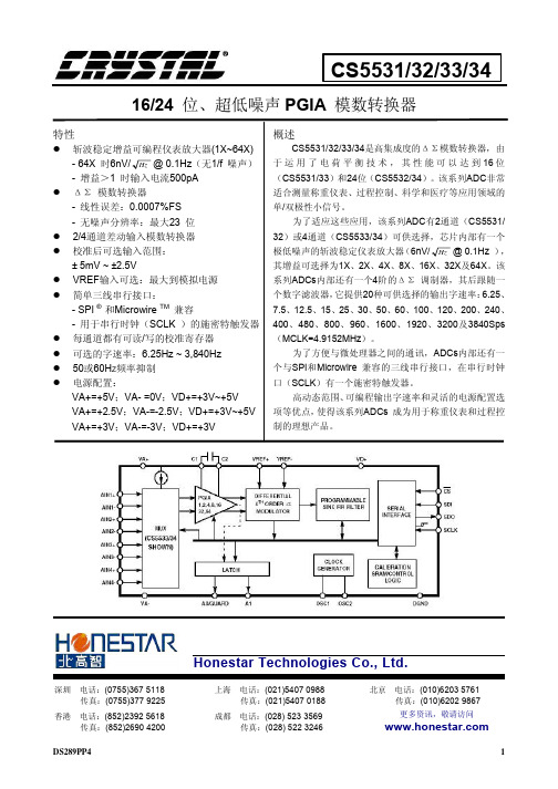
CS5531(5532_5533_5534)
最新欧姆龙E3JK系列光电开关
DC SSR负公共端DC48V 100mA以下漏泄电流0.1mA以下带负载短路保护
寿命
机械
5,000万次以上(开闭频率18,000次/小时)
电气
10万次以上(开闭频ຫໍສະໝຸດ 1,800次/小时)应答时间
30ms以下
10ms以下
30ms以下
耐电压
AC1,500V 50/60Hz 1min
振动
耐久
10~55Hz上下振幅1.5mmX、Y、Z各方向2h
误操作
10~55Hz上下振幅1.5mmX、Y、Z各方向2h
冲击
耐久
500m/s2 X、Y、Z各方向3次
误操作
100m/s2 X、Y、Z各方向3次
500m/s2 X、Y、Z各方向3次
100m/s2 X、Y、Z各方向3次
金属安装配件
铁
附属品
金属安装配件(带螺钉)、螺母、使用说明书、反射板(仅限回归反射型)
500m/s2 X、Y、Z各方向3次
100m/s2 X、Y、Z各方向3次
500m/s2 X、Y、Z各方向3次
100m/s2 X、Y、Z各方向3次
500m/s2 X、Y、Z各方向3次
保护结构
IEC规格IP64
连接方式
导线引出式(标准导线长2m)
质量(捆包状态)
约420g
约250g
材质
外壳
ABS
透镜部
丙烯酸酯树脂
电源电压
DC12~240V±10%脉动(p-p)10%以下、AC24~240V±10%50/60Hz
消耗电流
DC
3W以下
2W以下
FTC333C 触摸芯片
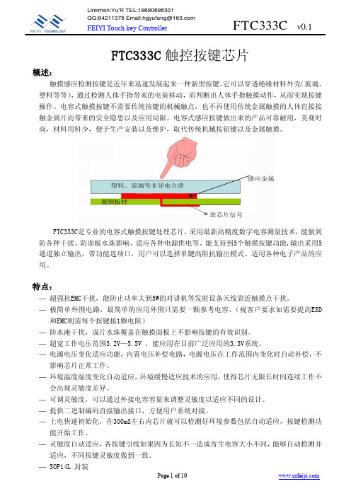
能开始工作。
— 灵敏度自动适应,各按键引线如果因为长短不一造成寄生电容大小不同,能够自动检测并
适应,不同按键灵敏度做到一致。
— SOP14L封装
Page 1 of 10
FEIYI Touch key Controller
管脚封装:
FTC333C v0.1
K1 1 K2 2 K3 3 K4 4 K5 5 GND 6 S1 7
改善电源最常用的简单RC滤波能起到高频滤波的作用,如下图:
※ 根据情况调整合适的 RC值,但要考虑 R会产生压降。蜂鸣器、LED等负载应该放到 R之前取电。
Page 5 of 10
FEIYI Touch key Controller
FTC333C v0.1
在该系统中,对触摸IC供电电源采用上述RC滤波(R=39/C=47Uf)电路处理后,触摸按键 非常稳定,测量电源端波形如上图。
影响芯片正常工作。
— 环境温度湿度变化自动适应,环境缓慢适应技术的应用,使得芯片无限长时间连续工作不
会出现灵敏度差异。
— 可调灵敏度,可以通过外接电容容量来调整灵敏度以适应不同的设计。
— 提供二进制编码直接输出接口,方便用户系统对接。
— 上电快速初始化,在300mS左右内芯片就可以检测好环境参数包括自动适应,按键检测功
2)触摸灵敏度与绝缘面板的厚度有关,同一介质的绝缘面板,厚度越薄灵敏度越高,
绝缘面板厚度越大,灵敏度越低。
3)触摸与按键感应盘的有效面积有关,面积越大,灵敏度越高,面积越小,灵敏度
越低。
在以上3个项目都固定的情况下,对芯片Cs电容容量进行调节也能获得不同的灵敏度。
芯片在运算的过程中需要采用Cs电容来做为基准参照,对Cs电容的调节能改变芯片运算,获
SC553资料
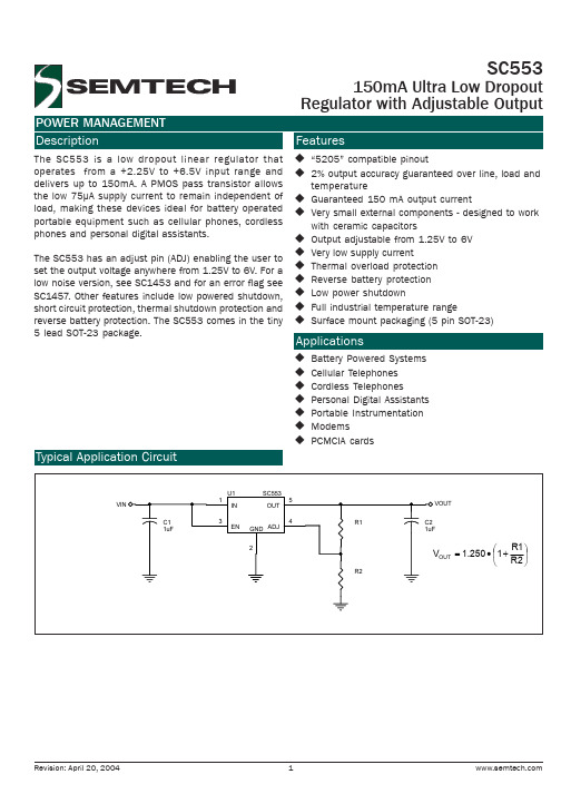
IQ(OFF)
VIN = 6.5V, VEN = 0V
0.1
1.0 1.5
µA
ADJ Adjust Pin Voltage (1) V AD J IOUT = 1mA 0mA ≤ IOUT ≤ 150mA, 2.25V ≤ VIN ≤ 5.5V Adjust Pin Input Current (2) IADJ VADJ = 1.3V -1.5% -2.0% 0.015 1.250 +1.5% +2.0% 2.500 5.000 OUT Line Regulation (1) REG(LINE) VIN = 2.25V to 5.5V, IOUT = 1mA, VADJ = VOUT 1.5 10 12 Load Regulation (1) REG(LOAD) IOUT = 0.1mA to 150mA, VIN = 2.25V, VADJ = VOUT
Notes: (1) Low duty cycle pulse testing with Kelvin connections required. (2) Guaranteed by design. (3) VOUT = 3.3V. Defined as the input to output differential at which the output voltage drops 100mV below the value measured at a differential of 1V. Not measurable on outputs set below 2.25V due to minimum VIN constraints. See Typical Characteristics for typical dropout voltage at other output voltage settings.
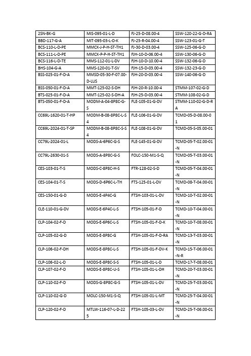
samtec型号
FJH-15-D-03.00-4
SSW-132-23-G-D
BSS-025-01-F-D-A
MMSD-05-30-F-07.00-D-LUS
FJH-20-D-03.00-4
SSW-140-06-G-D
BSS-050-01-F-D-A
MMT-125-02-S-DH
FJH-20-R-10.00-4
FTSH-140-02-F-D
TMM-114-01-L-D-RA
EHF-113-01-L-D-SM
SFM-125-02-S-D-A
FW-06-04-F-D-425-075
TMM-120-03-G-S
EHF-113-01-L-D-SM-LC
SFM-125-02-S-S-LC
FW-12-03-G-D-250-150
MODM-B-08-8P8C-L-S4
FLE-106-01-G-DV
TCMD-05-D-08.00-01
CC69L-2024-01-T-SP
MODM-B-08-8P8C-S-S4
FLE-108-01-G-DV
TCMD-05-S-05.00-01
CC79L-2024-01-L
MODS-A-6P6C-G-S
TFM-105-31-S-D
DWM-24-54-G-S-319
QTH-030-05-F-D-A
FTSH-117-01-L-DV
TFM-107-01-S-D-RA
DWM-25-54-G-S-319
QTH-030-08-F-D-A
FTSH-120-01-F-D
TFM-110-01-S-D
DWM-25-61-G-S-810
TFM-115-01-S-D
CCF-552M55FKE36资料
A 0.245 ± 0.020 [6.22 ± 0.51] 0.245 ± 0.020 [6.22 ± 0.51] 0.344 ± 0.031 [8.74 ± 0.79]
B 0.090 ± 0.008 [2.29 ± 0.20] 0.090 ± 0.008 [2.29 ± 0.20] 0.139 ± 0.009 [3.53 ± 0.23]
0.265 [6.73] 0.265 [6.73] 0.400 [10.16]
RESISTANCE VALUES
Vishay Dale Models CCF55 and CCF60 are available in the standard 96 resistance values per decade. Values are obtained from the following decade table by multiplying by powers of 10. As an example: 30.1 can represent 30.1 ohm, 301 ohm, 3.01 kohm, 30.1 kohm or 301 kohm. 10.0 10.2 10.5 10.7 11.0 11.3 11.5 11.8 12.1 12.4 12.7 13.0 13.3 13.7 14.0 14.3 14.7 15.0 15.4 15.8 16.2 16.5 16.9 17.4 17.8 18.2 18.7 19.1 19.6 20.0 20.5 21.0 21.5 22.1 22.6 23.2 23.7 24.3 24.9 25.5 26.1 26.7 27.4 28.0 28.7 29.4 30.1 30.9 31.6 32.4 33.2 34.0 34.8 35.7 36.5 37.4 38.3 39.2 40.2 41.2 42.2 43.2 44.2 45.3 46.4 47.5 48.7 49.9 51.1 52.3 53.6 54.9 56.2 57.6 59.0 60.4 61.9 63.4 64.9 66.5 68.1 69.8 71.5 73.2 75.0 76.8 78.7 80.6 82.5 84.5 86.6 88.7 90.9 93.1 95.3 97.6
comt336销售合同中的产品

一、产品概述本销售合同所涉及的产品为COMT336系列智能终端设备(以下简称“产品”)。
该产品由我国知名高新技术企业研发生产,具有高性能、高稳定性、易用性等特点,广泛应用于家庭、企业、政府等各个领域。
二、产品型号及配置1. COMT336A型- 主处理器:高性能八核处理器,主频高达2.0GHz- 内存:4GB DDR4- 存储:64GB eMMC- 屏幕尺寸:5.5英寸,1920×1080分辨率- 摄像头:后置1300万像素,前置500万像素- 电池:3000mAh,支持快充- 网络制式:支持4G全网通- 通信接口:USB Type-C、耳机接口、Micro-SD卡槽- 操作系统:Android 10.02. COMT336B型- 主处理器:高性能八核处理器,主频高达2.2GHz- 内存:6GB DDR4- 存储:128GB eMMC- 屏幕尺寸:6.5英寸,2400×1080分辨率- 摄像头:后置1600万像素,前置800万像素- 电池:4000mAh,支持快充- 网络制式:支持5G全网通- 通信接口:USB Type-C、耳机接口、Micro-SD卡槽- 操作系统:Android 11.0三、产品功能1. 高性能处理器:COMT336系列产品采用高性能处理器,确保系统运行流畅,满足用户在办公、娱乐、学习等场景下的需求。
2. 大容量存储:提供多种存储配置,满足用户对存储空间的不同需求。
3. 高清屏幕:采用高清屏幕,提供优质的视觉体验。
4. 高性能摄像头:后置高清摄像头,支持多种拍摄模式,满足用户拍照需求。
5. 快充技术:支持快充技术,充电速度快,节省用户时间。
6. 全网通网络制式:支持4G/5G全网通,满足用户在不同网络环境下的需求。
7. 丰富接口:提供USB Type-C、耳机接口、Micro-SD卡槽等接口,方便用户连接各种设备。
8. 智能操作系统:搭载Android操作系统,提供丰富的应用市场,满足用户个性化需求。
CS5463中文资料
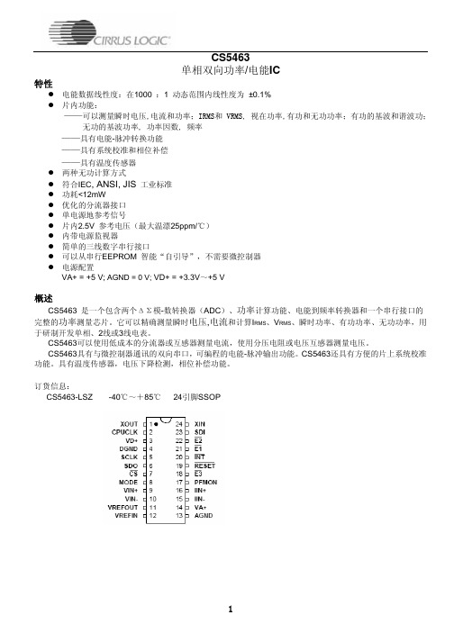
电压下跌电平在VSAGlevel寄存器中设定,电压下跌持续时间在VSAGduration寄存器中设定 电流下跌电平在ISAGlevel寄存器中设定,电流下跌持续时间在ISAGduration寄存器中设定 电压和电流下跌持续时间是指定在一个ADC周期之内。
两种无功计算方式
符合IEC, ANSI, JIS 工业标准
功耗<12mW 优化的分流器接口 单电源地参考信号 片内2.5V 参考电压(最大温漂25ppm/℃) 内带电源监视器 简单的三线数字串行接口 可以从串行EEPROM 智能“自引导”,不需要微控制器 电源配置 VA+ = +5 V; AGND = 0 V; VD+ = +3.3V~+5 V
3.1.校准寄存器
电压通道DC偏移量寄存器(Vdcoff)和电流通道DC偏移量寄存器(Idcoff)——存储进行加法运算的校正值, 用于校正当前的电压/电流通道的直流偏移量。当直流偏移量校准过程结束后,寄存器值由CS5463更新。
电压通道增益寄存器(Vgn)和电流通道增益寄存器(Ign)——存储进行乘法运算的校正值。该寄存器在交 流或直流增益校准后由CS5463进行更新。增益校准寄存器中的校准结果只能反映AC 和DC 增益校准结果中最新的 一次。这将意味着增益校准数据只有一个可加到CS5463通道中。因此用户在校准以前必须决定执行AC增益校准还
在每次计算周期结束时,DRDY位都将被置位(在状态寄存器中),同时若DRDY位未被屏蔽(在屏蔽寄存器中), INT 引脚将有效。
SF5539_规格书
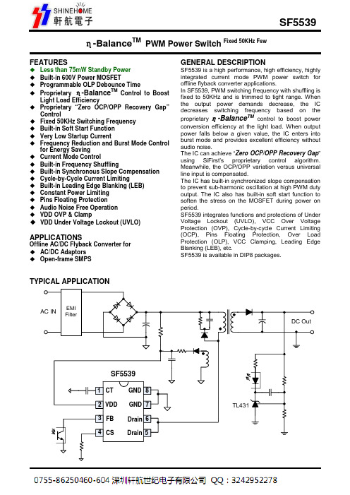
FEATURES◆Less than 75mW Standby Power◆Built-in 600V Power MOSFET◆Programmable OLP Debounce Time◆Proprietary η-Balance TM Control to BoostLight Load Efficiency◆Proprietary “Zero OCP/OPP Recovery Gap”Control◆Fixed 50KHz Switching Frequency◆Built-in Soft Start Function◆Very Low Startup Current◆Frequency Reduction and Burst Mode Controlfor Energy Saving◆Current Mode Control◆Built-in Frequency Shuffling◆Built-in Synchronous Slope Compensation◆Cycle-by-Cycle Current Limiting◆Built-in Leading Edge Blanking (LEB)◆Constant Power Limiting◆Pins Floating Protection◆Audio Noise Free Operation◆VDD OVP & Clamp◆VDD Under Voltage Lockout (UVLO) APPLICATIONSOffline AC/DC Flyback Converter for◆AC/DC Adaptors◆Open-frame SMPS GENERAL DESCRIPTIONSF5539 is a high performance, high efficiency, highly integrated current mode PWM power switch for offline flyback converter applications.In SF5539, PWM switching frequency with shuffling isfixed to 50KHz and is trimmed to tight range. When the output power demands decrease, the IC decreases switching frequency based on the proprietaryη-Balance TM control to boost power conversion efficiency at the light load. When outputpower falls below a given value, the IC enters into burst mode and provides excellent efficiency without audio noise.The IC can achieve “Zero OCP/OPP Recovery Gap” using SiFirst’s proprietary control algorithm. Meanwhile, the OCP/OPP variation versus universal line input is compensated.The IC has built-in synchronized slope compensation to prevent sub-harmonic oscillation at high PWM duty output. The IC also has built-in soft start function to soften the stress on the MOSFET during power on period.SF5539 integrates functions and protections of Under Voltage Lockout (UVLO), VCC Over Voltage Protection (OVP), Cycle-by-cycle Current Limiting (OCP), Pins Floating Protection, Over Load Protection (OLP), VCC Clamping, Leading Edge Blanking (LEB), etc.SF5539 is available in DIP8 packages.TYPICAL APPLICATIONη-Balance TM PWM Power Switch Fixed 50KHz FswPin ConfigurationCT VDDFB GND GND Drain CSDrain(1)Note 1. The Max. output power is limited by junction temperature Note 2. 230VAC or 100/115VAC with doublersNote 3. Typical continuous power in a non-ventilated enclosed adapter with sufficient drain pattern as a heatsink at 50 oC ambient.Note 4. Max. practical continuous power in a open-frame design with sufficient drain pattern as a heat sink at50 oC ambient.Marking InformationYWW: Year&Week codeBlock DiagramELECTRICAL CHARACTERISTICS ONote 5. Stresses beyond those listed under “Absolute Maximum Ratings” may cause permanent damage to the device. These are stress ratings only, and functional operation of the device at these or any other conditions beyond those indicated in the operational sections of the specifications is not implied.Exposure to absolute maximum rating conditions for extended periods may affect device reliability. Note 6. The device is not guaranteed to function outside its operating conditions.Note 7. Guaranteed by design.Note 8. These parameters, although guaranteed, are not 100% tested in productionCHARACTERIZATION PLOTSOPERATION DESCRIPTIONSF5539 is a high performance, high efficiency, highly integrated current mode PWM power switch for offline flyback converter applications. The built-in advanced energy saving with high level protection features improves the SMPS reliability and performance without increasing the system cost.◆ UVLO and Startup OperationFig.1 shows a typical startup circuit. Before the IC begins switching operation, it consumes only startup current (typically 3uA) and current supplied through the startup resistor Rst charges the VDD hold-up capacitor Cdd. When VDD reaches UVLO turn-on voltage of 15.5V(typical), SF5539 begins switching and the IC current consumed increased to 2mA (typical). The hold-up capacitor Cdd continues to supply VDD before the energy can be delivered from auxiliary winding Na. During this process, VDD must not drop below UVLO turn-off voltage (typical 9V). The selection of Rst and Cdd should be a trade off between the power loss andFig.1◆ Low Operating CurrentThe operating current in SF5539 is as small as 2mA (typical). The small operating current results in higher efficiency and reduces the VDD hold-up capacitance requirement.◆ Soft StartSF5539 features an internal 4ms (typical) soft start that slowly increases the threshold of cycle-by-cycle current limiting comparator during startup sequence. It helps to prevent transformer saturation and reduce the stress on the secondary diode during startup. Every restart attempt is followed by a soft start activation.◆ “Zero OCP/OPP Recovery Gap” ControlThe definition of OCP or OPP recovery gap of a power adaptor is illustrated in Fig.2. At T0, assuming an adaptor is at full loading mode. If the loading keeps increasing, then the system will output maximum power P_opp, which will trigger OPP protection at the same time. After the OPP protection is triggered, usually the system will enter into the auto-recovery mode, in burst manner. If the system power demand decreases below P_recovery, then system will enter into normal mode again, as shown in Fig.2. The difference between P_opp and P_recovery is defined as “OPP Recovery Gap ”, which can cause system startup failure especially in 90VAC full load startup.T1T2T0P_full_loadP_oppFig.2SF5539 can achieve “Zero OCP/OPP Recovery Gap ” in the whole universal AC input range using SiFirst’s proprietary control algorithm.◆ Oscillator with Frequency ShufflingPWM switching frequency in SF5539 is fixed to 50KHz and is trimmed to tight range. To improve system EMI performance, SF5539 operates the system with ±4% frequency shuffling around setting frequency.◆ Synchronous Slope CompensationInSF5539, the synchronous slope compensation circuit is integrated by adding voltage ramp onto the current sense input voltage for PWM generation. This greatly improves the close loop stability at CCM and prevents the sub-harmonic oscillation and thus reduces the output ripple voltage.◆ Programmable OLP Debounce TimeConnecting a capacitor C CT from CT pin to GND according to the equation below to program the OLP debounce time. In OLP debounce time, an internal current (14uA, typical) charges C CT , when CT pin voltage reaches 3V, an internal 55ms debounce is triggered. When internal 55ms debounce time is over, the OLP protection is triggered and the system will enter into auto recovery protection mode.ms 5514uAC *3V T CTce OLP_deboun +=If CT pin is floating, the OLP debounce time is 55ms. Otherwise, the OLP debounce time can be programmed by CT capacitor.◆ Leading Edge Blanking (LEB)Each time the power MOSFET is switched on, a turn-on spike occurs across the sensing resistor. The spike is caused by primary side capacitance and secondary side rectifier reverse recovery. To avoid premature termination of the switching pulse, an internal leading edge blanking circuit is built in. During this blanking period (250ns, typical), the PWM comparator is disabled and cannot switch off the gate driver. Thus, external RC filter with a small time constant is enough for current sensing.◆ Proprietary η-Balance TM ControlThe efficiency requirement of power conversion is becoming tighter than before. These new energy standards focus on the average efficiency of the whole loading range. Therefore, the light load efficiency is becoming more and more important.In SF5539, a proprietary η-Balance TMcontrol is integrated to boost the light load efficiency. As shown in Fig.3, when the loading becomes light, the IC will reduce the PWM switching frequency according to an optimized frequency reduction curve. The specific frequency reduction curve and the power at a frequency are determined by theoutput of η-Balance TMcontrol. For example, P1 is at full load, P2 is at 75% full load, P3 and P4 are 50% and 25% full load respectively. The η-Balance TM control can provide higher average efficiency than conventional frequency reduction technique, as illustrated in Fig.365kHzBurst mode22kHzFrequency Reduction modeNormal modeFig.3◆ Burst Mode ControlWhen the loading is very small, the system enters into burst mode. When VFB drops below Vskip, SF5539 will stop switching and output voltage starts to drop, which causes the VFB to rise. Once VFB rises above Vskip, switching resumes. Burst mode control alternately enables and disables switching, thereby reducing switching loss in standby mode.Fig.4◆Auto Recovery Mode ProtectionAs shown in Fig.5, once a fault condition is detected, switching will stop. This will cause VDD to fall because no power is delivered form the auxiliary winding. When VDD falls to UVLO(off) (typical 9V), the protection is reset and the operating current reduces to the startup current, which causes VDD to rise, as shown in Fig.4. However, if the fault still exists, the system will experience the above mentioned process. If the fault has gone, the system resumes normal operation. In this manner, the auto restart can alternatively enable and disable the switching until the fault condition is disappeared.Fig.5◆VDD OVP(Over Voltage Protection)VDD OVP (Over Voltage Protection) is implemented in SF5539 and it is a protection of auto-recovery mode.◆Over Load Protection (OLP) / OverCurrent Protection (OCP) / Over PowerProtection (OPP) / Open Loop Protection (OLP)When OLP/OCP/OPP/Open Loop occurs, a fault is detected. If this fault is present for more than ceOLP_debounT, the protection will be triggered, the IC will experience an auto-recovery mode protection as mentioned above, as shown in Fig.6. The ceOLP_debounT debounce time is to prevent the false trigger from the power-on and turn-off transient.Fig.6◆Soft Gate DriveThe driving stage of SF5539 is a soft totem-pole gate driver to minimize EMI. Cross conduction has been avoided to minimize heat dissipation, increase efficiency, and enhance reliability.SF1539 PACKAGE MECHANICAL DATASF1539IMPORTANT NOTICESiFirst Technology Nanhai, Ltd (SiFirst) reserves the right to make corrections, modifications, enhancements, improvements and other changes to its products and services at any time and to discontinue any product or service without notice. Customers should obtain the latest relevant information before placing orders and should verify that such information is current and complete.SiFirst warrants performance of its hardware products to the specifications applicable at the time of sale in accordance with SiFirst’s standard warranty. Testing and other quality control techniques are used to the extent SiFirst deems necessary to support this warranty. Except where mandated by government requirements, testing of all parameters of each product is not necessarily performed.SiFirst assumes no liability for application assistance or customer product design. Customers are responsible for their products and applications using SiFirst’s components. To minimize the risks associated with customer products and applications, customers should provide adequate design and operating safeguards. Reproduction of SiFirst’s information in SiFirst’s data books or data sheets is permissible only if reproduction is without alteration and is accompanied by all associated warranties, conditions, limitations, and notices. Reproduction of this information with alteration is an unfair and deceptive business practice. SiFirst is not responsible or liable for such altered documentation. Information of third parties may be subject to additional restrictions.Resale of SiFirst’s products or services with statements different from or beyond the parameters stated by SiFirst for that product or service voids all express and any implied warranties for the associated SiFirst’s product or service and is an unfair and deceptive business practice. SiFirst is not responsible or liable for any such statements.SiFirst’s products are neither designed nor intended for use in military applications. SiFirst will not be held liable for any damages or claims resulting from the use of its products in military applications.SiFirst’s products are not designed to be used as components in devices intended to support or sustain human life. SiFirst will not be held liable for any damages or claims resulting from the use of its products in medical applications.。
FRAKO产品手册(2012)
外形尺寸
26
典型方案
26
有源滤波器
27
产品优势
27
选型表
28
安装和接线
29
典型方案
29
全球业绩
30
联系我们
31
目 录
公 司 简 介
滤波 补偿 模块
FRAKO 公司简介
滤波 补偿
套件
FRAKO公司是德国从事电网质量控制和检测的专业制造公司,成立于1928年。至今有
80多年的历史,主要产品为电容器、控制器、电抗器、补偿模块、电容补偿成套装置,有源
器
ISO9001体系认证。
自
动
德国金米勒公司与FRAKO公司结成全球战略合作伙伴,相互合作、全力支持。我们一
补
直是你们的最佳合作伙伴,不仅提供优质的产品,同时提供完善的服务,包含项目计划编
偿 仪
制,方案咨询与设计,现场测量等。秉承安全为本的宗旨,我们以保证产品质量为己任,并
根据不同的用户要求,有针对性地提供完美的解决方案。
KIT50-400-7S 50 72A 50 264 88 235 140 120 27 70/85 225/320 7%
KIT25-400-14S 25 36A 25 264 88 235 140 120 27 70
225 14%
KIT50-400-14S 50 72A 50 300 100 265 164 144 33 70
KIT50-400-7S
8
滤波 补偿
1600
500
EMR1100/S
KIT50-400-7S
10
套件
2000
600
EMR1100/S
KIT50-400-7S
Software instruction manual of NCR-333 NAVTEX PC R
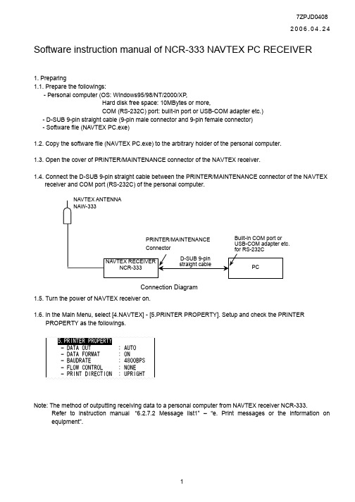
2006.04.24Software instruction manual of NCR-333 NAVTEX PC RECEIVER1. Preparing1.1. Prepare the followings:- Personal computer (OS: Windows95/98/NT/2000/XP ,Hard disk free space: 10MBytes or more, COM (RS-232C) port: built-in port or USB-COM adapter etc.) - D-SUB 9-pin straight cable (9-pin male connector and 9-pin female connector) - Software file (NAVTEX PC.exe)1.2. Copy the software file (NAVTEX PC.exe) to the arbitrary holder of the personal computer.1.3. Open the cover of PRINTER/MAINTENANCE connector of the NAVTEX receiver.1.4. Connect the D-SUB 9-pin straight cable between the PRINTER/MAINTENANCE connector of the NAVTEX receiver and COM port (RS-232C) of the personal computer.1.5. Turn the power of NAVTEX receiver on.1.6. In the Main Menu, select [4.NAVTEX] - [5.PRINTER PROPERTY]. Setup and check the PRINTER PROPERTY as the followings.Note: The method of outputting receiving data to a personal computer from NAVTEX receiver NCR-333.Refer to instruction manual “6.2.7.2 Message list1” – “e. Print messages or the information onequipment”.- DATA OUT : AUTO- DATA FORMAT : ON- BAUDRATE : 4800BPS- FLOW CONTROL : NONE- PRINT DIRECTION : UPRIGHTConnection Diagram1.7 If any other applications are operating on the personal computer close them. And then start the software file(NAVTEX PC.exe).Select “View” –“Size” menu, and select the size of the software screen.1.8 Select “COM Port” menu, and then select the connected COM port number, 4800bps for baudrate and FlowOFF.2. Display of NAVTEX messageReceived NAVTEX messages can be displayed.2.1. Click "Msg list" on the left side screen.2.2. Select a NAVTEX message from the message list. Selected message title is marked with gray.2.3. Double click the message title to display the NAVTEX message.2.32.12.2Total msg number Set of sortInputStationList reverse3. Printing of NAVTEX MessageNAVTEX messages can be printed by the three methods as the followings 3.1-3.3.NAVTEX message list can be printed by the method of 3.4.3.1. Double click the NAVTEX message title to display the NAVTEX message, and thenselect “File” –“Print” menu to print.3.2. Click "Msg list" on the left side screen. Click the message title to select. In the case of multiple selection,click the title while pressing the “Ctrl” key to add the selection.Right click, and then select “Print Menu”- “Select Msg”.3.3. Click "Msg list" on the left side screen.Right click and select “Print Menu”- “Batch Print”.Select channel, station and message type to print.Click the “PRINT” button.3.4. Click "Msg list" on the left side screen.Right click, and then select “Print Menu”- “Msg List”.4. MenuMenu has the following four items of setup and display.1. Rx Station Setting of received stations.2. Rx Msg Type Setting of message types.3. Navtex Log Display of the Self-diagnosis and alarm information.4. Data clear Reset of each contents data.4.1. Click "Rx Station" on the left side screen. Select and set received stations to display messages.Select receive channel.レ SelectレNon select4.2. Click "Rx Msg Type" on the left side screen. Select and set received message types to display messages.Select receive channel.レ SelectレNon select4.3. Click "Navtex Log" on the left side screen.Click each contents (Self Diagnosis, Alarm, Alarm History, Status) to display.They are displayed after performing the following operation on the NAVTEX receiver NCR-333.1.Self Diagnosis : In the Main Menu of the NCR-333, select [5.MAINTENANCE] –[1.SELF DIAGNOSIS] to select “ST-PRTN”.2.Alarm : In the Main Menu of the NCR-333, select [5.MAINTENANCE] –[2.NAVTEX ALARM].Press “*” key and then select “PRINT OUT”.(In the case of “NO DATA”, it does not output data.)3.Alarm History : In the Main Menu of the NCR-333, select [5.MAINTENANCE] –[2.NAVTEX ALARM].Press “*” key and then select “HISTORY” - “PRINT OUT”.(In the case of “NO DATA”, it does not output data.)4.Status : In the Main Menu of the NCR-333, select [5.MAINTENANCE] - [3.STATUS].Press “*” key and then select “PRINT OUT”.4.4. Click "Data Clear" on the left side screen. Click the each button to reset the each data.All Message Clear : Reset of the all message.Navtexl Log Clear : Reset of the Navtex log (Self-diagnosis, alarm,etc).Config Clear : Reset of the config (Com port, baudrate, flow, size,Rx station,msg type).All Clear : Reset of the all message, Navtex log and configuration.。
摩尔克斯易取FPC FFC连接器产品说明说明书
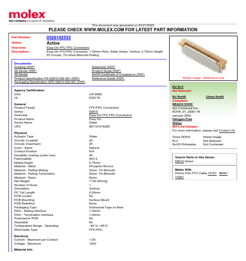
Series image - Reference only
EU ELV Not Relevant
EU RoHS
China RoHS
Compliant
REACH SVHC
Not Contained Per -
ECHA_01_2020 (16
January 2020
Halogen-Free
Physical Actuator Type Circuits (Loaded) Circuits (maximum) Color - Resin Contact Position Durability (mating cycles max) Flammability Mated Height Material - Metal Material - Plating Mating Material - Plating Termination Material - Resin Net Weight Number of Rows Orientation PC Tail Length PCB Locator PCB Mounting PCB Retention Packaging Type Pitch - Mating Interface Pitch - Termination Interface Polarized to PCB Stackable Temperature Range - Operating Wire/Cable Type
Part Number:
Status:
Overview: Description:
This document was generated on 02/27 Nhomakorabea2020
PLEASE CHECK FOR LATEST PART INFORMATION
一种基于DSP和采样ADC的数字锁定放大器

一种基于DSP和采样ADC的数字锁定放大器
胡绍民;张广发
【期刊名称】《数据采集与处理》
【年(卷),期】2000(015)002
【摘要】探讨了用DSP(数字信号处理器)和采样ADC(模数转换器)实现数字锁定放大器的一种方法.在整数个周期内对被测信号进行采样得到信号序列,由数学运算得到参考序列,通过计算信号序列和参考序列的互相关函数就可实现数字相敏检测.文中还对数字相敏检测的频率特性进行了分析.最后,给出了实际设计的数字锁定放大器,它的工作频率范围是10 Hz~30 kHz,实验结果表明,可以用它来测量低信噪比的信号.
【总页数】4页(P222-225)
【作者】胡绍民;张广发
【作者单位】国防科技大学应用物理系,长沙,410073;国防科技大学应用物理系,长沙,410073
【正文语种】中文
【中图分类】TN911.72
【相关文献】
1.基于DSP的ADC模块采样校正算法的研究 [J], 董仕鹏;陈璇
2.基于数字后处理算法的并行交替采样ADC系统 [J], 周浩;赵雷;李玉生;刘树彬;安琪
3.基于DSP的单ADC数字功率因数校正器研究 [J], 沈黎韬;陶雪慧;杨斌
4.基于DSP的ADC采样校正与显示系统 [J], 姜建国;赵宇
5.一种基于ADC采样的设备ID识别方法 [J], 陈超鑫;肖林松;周学成;陈岗
因版权原因,仅展示原文概要,查看原文内容请购买。
- 1、下载文档前请自行甄别文档内容的完整性,平台不提供额外的编辑、内容补充、找答案等附加服务。
- 2、"仅部分预览"的文档,不可在线预览部分如存在完整性等问题,可反馈申请退款(可完整预览的文档不适用该条件!)。
- 3、如文档侵犯您的权益,请联系客服反馈,我们会尽快为您处理(人工客服工作时间:9:00-18:30)。
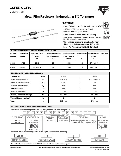
CCF55, CCF60
Vishay Dale
Metal Film Resistors, Industrial, ± 1% Tolerance
FEATURES
• Power Ratings: 1/4, 1/2, 3/4 and 1 watt at + 70°C • ± 100ppm/°C temperature coefficient • Superior electrical performance • Flame retardant epoxy conformal coating • Standard 5 band color code marking for ease of identification after mounting • Tape and reel packaging for automatic insertion (52.4mm inside tape spacing per EIA-296-E) • Lead (Pb)-Free version is RoHS Compliant
Pb-free Available
e3
RoHS*
COMPLIANT
STANDARD ELECTRICALБайду номын сангаасSPECIFICATIONS
GLOBAL MODEL HISTORICAL MODEL POWER RATING P70˚C W 0.25 / 0.5 0.50 / 0.75 / 1.0 LIMITING ELEMENT VOLTAGE MAX. V 250 500 TEMPERATURE COEFFICIENT ppm/°C ± 100 ± 100 TOLERANCE % ±1 ±1 RESISTANCE RANGE E-SERIES
TOLERANCE CODE F = ± 1%
TEMPERATURE COEFFICIENT K = 100ppm
E36 = Lead (Pb)-Free, T/R (5000 pcs) R36 = Tin/Lead, T/R (5000 pcs)
Historical Part Number example: CCF-553010F (will continue to be accepted)
100 80 60 40 20 0 -65 -50 -25 0 25 50 70 75 100 125 150 165 175 200 AMBIENT TEMPERATURE IN ˚C
DERATING MARKING
— Color band
PERFORMANCE
POWER RATING @ + 70°C CCF55 CCF60 TEST* Thermal Shock Short Time Overload Low Temperature Operation Moisture Resistance Resistance to Soldering Heat Shock / Bump Vibration Life Terminal Strength Dielectric Withstanding Voltage 1/4 watt 1/2 watt MAXIMUM ∆R ± 0.5% ± 0.5% ± 0.5% ± 1.5% ± 0.5% ± 0.5% ± 0.5% ± 0.5% ± 0.2% ± 0.5% 1/2 watt 3/4 watt and 1 watt MAXIMUM ∆R ± 1.0% -
Ω
10R - 3.01M 10R - 1M 96 96
CCF55 CCF60
CCF-55 CCF-60
TECHNICAL SPECIFICATIONS
PARAMETER Rated Dissipation at 70˚C Maximum Working Voltage Insulation Voltage (1min) Dielectric Strength Insulation Resistance Operating Temperature Range Terminal Strength (pull test) Weight UNIT W V Veff VAC Ω °C lb g CCF55 0.25 / 0.5 ≤ 250 500 450 ≥10
A 0.245 ± 0.020 [6.22 ± 0.51] 0.245 ± 0.020 [6.22 ± 0.51] 0.344 ± 0.031 [8.74 ± 0.79]
B 0.090 ± 0.008 [2.29 ± 0.20] 0.090 ± 0.008 [2.29 ± 0.20] 0.139 ± 0.009 [3.53 ± 0.23]
RATED POWER IN %
120
C
(Max.)
D 0.025 ± 0.002 [0.64 ± 0.05] 0.023 ± 0.002 [0.60 ± 0.05] 0.025 ± 0.002 [0.64 ± 0.05]
E 1.100 ± 0.040 [27.94 ± 1.02] 1.100 ± 0.040 [27.94 ± 1.02] 1.000 ± 0.040 [25.40 ± 1.02]
17
C
GLOBAL MODEL CCF55 CCF60
C
F
5
5
3
0
1
R
F
K
R
3
6
PACKAGING SPECIAL Blank = Standard (Dash Number) (up to 3 digits) From 1-999 as applicable
RESISTANCE VALUE R = Decimal K = Thousand M = Million 10R0 = 10Ω 680K = 680KΩ 1M00 = 1.0MΩ
* Test Methods per MIL-STD-202G/IEC 60115/DIN EN 140000 (as applicable).
Document Number: 31015 Revision 05-Oct-05
For Technical Questions, contact ff3dresistors@
0.265 [6.73] 0.265 [6.73] 0.400 [10.16]
RESISTANCE VALUES
Vishay Dale Models CCF55 and CCF60 are available in the standard 96 resistance values per decade. Values are obtained from the following decade table by multiplying by powers of 10. As an example: 30.1 can represent 30.1 ohm, 301 ohm, 3.01 kohm, 30.1 kohm or 301 kohm. 10.0 10.2 10.5 10.7 11.0 11.3 11.5 11.8 12.1 12.4 12.7 13.0 13.3 13.7 14.0 14.3 14.7 15.0 15.4 15.8 16.2 16.5 16.9 17.4 17.8 18.2 18.7 19.1 19.6 20.0 20.5 21.0 21.5 22.1 22.6 23.2 23.7 24.3 24.9 25.5 26.1 26.7 27.4 28.0 28.7 29.4 30.1 30.9 31.6 32.4 33.2 34.0 34.8 35.7 36.5 37.4 38.3 39.2 40.2 41.2 42.2 43.2 44.2 45.3 46.4 47.5 48.7 49.9 51.1 52.3 53.6 54.9 56.2 57.6 59.0 60.4 61.9 63.4 64.9 66.5 68.1 69.8 71.5 73.2 75.0 76.8 78.7 80.6 82.5 84.5 86.6 88.7 90.9 93.1 95.3 97.6
11
CCF60 0.5 / 0.75 / 1.0 ≤ 500 500 450 ≥1011 -65 / +165 2 0.75 max
-65 / +165 2 0.35 max
GLOBAL PART NUMBER INFORMATION
New Global Part Numbering: CCF55301RFKR36 (preferred part numbering format)
CCF-55
HISTORICAL MODEL
3010
RESISTANCE VALUE
F
TOLERANCE CODE
R36
PACKAGING
* Pb containing terminations are not RoHs compliant, exemptions may apply
16 For Technical Questions, contact ff3dresistors@ Document Number: 31015 Revision 05-Oct-05
元器件交易网
CCF55, CCF60
Metal Film Resistors, Industrial, ± 1% Tolerance
DIMENSIONS in inches [millimeters]
A E
Vishay Dale
C Max.
B
D
GLOBAL MODEL CCF55 (Sn/Pb) CCF55 (Sn) CCF60
