82559ER
APQ-0.4.1用户手册

f. 接 下 来 , 先 返 回 主 界 面 。 然 后 在 主 界 面 点 击 选 择 “APQ-XP”。这时,就会进入一个终端,并看到“$”提 示符后面有一条命令,这就是刚才我们输入到“登录后自 动运行”里的那条命令,回车后就能启动 APQ 了。(左 图)
如 果 装 有 root 权 限 管 理 应 用 , 第 一 次 会 提 示 ConnectBot 要获取 root 权限,请一定要给它 root 权限, 否则可能不能启动 APQ 或运行不稳定。
如果没有任何提示(如下图),说明你已经运行成功了。如果出现“虚拟机已关闭, 但是中间出现错误”,说明运行失败,需要根据提示检查出错原因。
关于如何写虚拟机配置文件,请参考下一节的第三部分第 1 小节。 3. 如果你不是从其它地方下载的镜像,没有相应的配置文件,你可以自己创建相应的.conf 文 件,可以通过复制 APQ 目录下原来的.conf 文件,改名,再对内容根据实际情况修改。
终端下使用说明
一、使用流程介绍
准备: 下载解压软件和镜像文件。 安装终端应用、VNC 客户端应用。
2.2 连接图形界面 a. 打开汉化版的 VNC 查看器,点左下角的“+”, 添加一个新的连接。(右图)
b. 地址栏里写“localhost”,名称自己随便取,比如这 里写成“APQ-XP”,然后点左下角的勾保存。(左图)
c. 接下来就点“连接”(左下图)。以后每次进入后,直接点“APQ-XP”(右下图)。
APQ-0.3.1.zip 比 APQ-0.3.zip 新。下载最新版 APQ-0.3.2.zip 一个文件即可。
8255芯片知识点总结

8255芯片知识点总结一、8255芯片的功能8255芯片的主要功能是实现微处理器与外部设备之间的数据传输和交互。
它提供了24个I/O引脚,可配置为三个8位的并行输入/输出端口。
除了I/O功能之外,8255芯片还具有自动手摇功能,可通过设置控制字来进行不同模式的操作,包括模式0(基本I/O)、模式1(手摇方式)、模式2(双向通讯)和模式3(快速反射)。
在基本I/O模式下,8255芯片的三个端口A、B、C分别作为输出、输入、控制端口。
通过设置控制字可以配置每个端口的工作方式,包括输入、输出和双向通讯。
而在手摇方式下,8255芯片可以通过设置手摇信号来进行数据传输,可以实现16位数据的传输操作。
在双向通讯模式下,8255芯片可以通过读写控制字来实现双向数据传输。
而在快速反射模式下,8255芯片可以实现数据的快速输入和输出,适用于数据采集和高速数据传输等场景。
除了上述功能,8255芯片还可以实现对外设设备的中断请求响应、电源管理和自检功能等。
因此,8255芯片在微处理器系统中扮演着非常重要的角色,可以实现微处理器与外部设备的高效通讯和控制。
二、8255芯片的特点8255芯片具有以下几个显著的特点:1. 多功能性:8255芯片提供了多种工作模式和配置方式,可以适用于不同的应用场景。
用户可以通过编程来设置控制字,实现8255芯片的不同功能。
2. 高性能:8255芯片具有高速的数据传输和处理能力,可以满足对数据传输速度要求较高的应用。
3. 可编程性:8255芯片的功能和工作方式可以通过编程进行配置,可以根据具体的应用需求来设置控制字,实现不同的功能和模式。
4. 可靠性:8255芯片具有良好的稳定性和可靠性,可以在恶劣的环境条件下正常工作。
5. 兼容性:8255芯片广泛应用于各种微处理器系统中,与不同的微处理器兼容性强,可广泛应用于各种系统。
6. 低功耗:8255芯片采用低功耗设计,具有较低的能耗,适用于对电源管理要求较高的应用。
F106-趋势科技-NVWE_FAQ_All0622
Network VirusWall 1200 FAQ第一、一般营销问题问题:如今客户所面临的最大安全问题是什么?答: 各种组织都面临下面三项挑战:1、网络病毒(互联网蠕虫),比如正在困扰全球组织的Blaster 和Slammer。
根据Computer Economics的估算,仅这两种病毒在2003年造成的损失就高达21.5亿美元。
2、从发现漏洞到病毒发作之间的时间越来越短。
例如,从发现Nimdas 所利用的漏洞到Nimda 出现之间的时间为一年。
而Blaster 仅不到一个月。
3、来自网络中旧病毒循环传播的反复感染依然令人头疼,而未经保护的设备通过多个进入点接入网络的情况使这一问题继续恶化。
2003年排名前十位的病毒中有一半早在1-4年前就已出现。
问题:什么是网络病毒?答:1、当数据沿网络从一台计算机传往另一台计算机时,它就像拼图一样被分解为小的信息包或片断,然后在到达目的地后重组为一个完整文件。
诸如Blaster 或Slammer 等网络病毒可以隐藏在这些信息包中,从而不受监视地进入目标系统,并可在全部信息包重组为传统防病毒解决方案可以扫描的完整文件之前就开始制造混乱。
2、网络病毒使用诸如TCP/UDP 等网络端口,并能够利用安全漏洞来复制传播和进行感染。
3、与Sobig 或MyDoom 等群发邮件型的病毒不同,网络病毒并不需要用户点击电子邮件附件。
问题:为什么趋势科技将网络病毒视为最大的安全问题?答:1、自2001年起,尽管各种组织都投资了各式各样的安全技术,但是网络病毒问题目前仍未得到解决。
2、对于某些组织而言,他们需要三个月的时间来清除Blaster 病毒,因为他们缺乏能够监视这些攻击、封堵病毒传播的路径以及消除和清除感染的综合解决方案。
3、随着软件漏洞数量的增多,网络病毒攻击携带恶性有效负荷的可能性就越大。
问题:Network VirusWall 如何来解决这个最大的安全问题?答:Network VirusWall 可以通过下列功能来解决这个问题:1、在发作期间封堵高威胁性的漏洞(未安装补丁的计算机)。
8255芯片引脚及其功能

8255芯片引脚及其功能
8255是一个40引脚的双列直插式芯片,图8-8为8255与80C51的连接图。
由于80C51与8255的连接就是3总线的连接。
8255的数据总线DB有8根:D0~D7。
因为80C51是用其P0口作为数据总线口,所以80C51与8255数据线连接为:80C51 的P0.0~P0.7与8255的D0~D7连接。
8255地址线AB有2根:A0~A1。
A0、A1通过74LS373锁存器与80C51的P0.0、P0.1连接。
A1A0取00~11值,可选择A、B、C口与控制寄存器,选择方法如下:
①片选信号<?XML:NAMESPACE PREFIX = V /> <?XML:NAMESPACE PREFIX = O /> :由P2.5~P2.7经138译码器产生。
若要选中8255,则必须有效,此时2.5P2.6P2.7=111。
由此可推知各口地址如下:
A口:111 x~x 00 = E000H (当x~x=0~0时)
B口:111 x~x 01 = E001H (当x~x=0~0时)
C口:111 x~x 10 = E002H (当x~x=0~0时)
控制口:111 x~x 11 = E003H (当x~x=0~0时)
其中x~x表示取值可任意,所以各口地址不是唯一。
②读信号:8255的读信号与80C51的相连。
③写信号:8255的写信号与80C51的相连。
④复位信号RST:8255的复位信号RST与80C51的RST 相连。
VxWorks系统下的Intel82559ER驱动程序设计
代码 ,但没有提供 8 5 9的驱动源代码 , 2 5 芯片供应 商也仅提供 了基于 MP 7 x的 目 C5
每秒进或出数据 包 1 o 0 p (a k t p r 2 0 p sp c es e scn ) e o d ,且 CP 占用率不高于 6 %。 U 0 本单 板 采 用 的软 件 平 台 为 W n d i
R i r公 司 的 V XW kS操 作 系统 , Ve 0r
u i 则是用来转发 由话音信号打成的数据 nt 2
包 的 , 即 以太 网 包 从 u i1 ,从 u i2 nt 进 n t
出 , 或 从 u i 2进 ,从 u i 1出 , 要 求 nt nt
套Hale Waihona Puke l l| | 的驱动也小同。wid Rie 公司提供 了 n vr
85 7 M P 84 U平 台上 的 驱 动 源 25 在 C 2 x CP
MP 241 的 硬 件 平 台 ,提 出一 种 新 的 C8 CP U Ie 2 5 E n 1 5 9 R快 速 以太 网控 制 器驱 动程 序 设 计 t8
换机的 络接 口。8 5 9在 Vx r s系 25 Wo k
统 下 的 驱 动 与 CPU 型号 有 很 大 的 关 系 , 譬 如 在 x 6系 列 C U 与 Moooa公 司的 8 P tr l P we P 系 列 C o rC PU 硬 件 平 台 上 ,8 5 9 2 5
网 口处理 数 据 包的 能 力 , 又避 免 了C U占 用率 P
VCU100技术说明
1.VCU100概述:VCU 100(vehicle control unit)是专为Automated Guided V ehicle (AGV)控制和应用而设计的工业PC,它的结构组成符合工业级技术发展的要求适合在工业环境下使用,VCU100也是AGV系统的主控制单元。
2.技术数据:这一章节主要介绍关于CPU卡,通信口和电源的特性。
表2-1:CPU其采用CXl-300MHz作为板上处理器,高性能Intel 82559ER芯片组,支持VGA/LCD,网络及固态电子盘(CF卡),AGV的主程序以及参数文件、引导文件存储在CF卡上作为AGV的控制软件。
VCU100提供通讯接口:两个串口(RS232 COM-port),和两个CAN总线接口。
另外VCU100还有LAN(局域网)接口,VGA(显示器)接口和PS/2(键盘)接口。
表2-2:通讯VCU100内部的VGA和TFFIO/IOOBASE-T快速以太网(Fast Ethernet)芯片。
可连接LCD显示屏作为AGV的显示终端,进行人机交互和状态显示,网口连接无线电台可以与上位机进行无线以太网联机,实现对AGV的调度。
VCU100内部使用的104总线CAN通讯卡,可实现中心处理单元与各信号采集单元间的数据交换。
其具备两个CAN口能同时操作两个独立的CAN 网络,在端口上方有状态指示灯。
表2-3:电源VCU100工作电源为直流的24V,板载低功耗CPU,可无风扇工作。
3.物理尺寸15图3-1:VCU100尺寸4.外部指示和连接器您可以通过观察VCU100上的LED指示灯判断VCU100的工作状态。
图4-1:VCU100连接器4.1 COM(串口)1,2串口上方的LED指示受软件控制。
所反映的状态信息取决于该串口连接的设备。
LED闪烁表示该串口正在通讯。
表4-1:串口1,2 LED指示4.2 CAN总线接口CAN总线2接口为预留接口表4-2:CAN总线1,2及LED指示4.3 系统LED指示除了连接器的LED指示外,VCU100上还有系统的状态LED指示灯,其状态描述如下。
ETHERCAT支持的网卡芯片
支持EtherCAT的intel 网卡列表(芯片型号) Supported Network Controller by Beckhoff Ethernet Driver Intel Fast Ethernet Controllers (Vendor ID: 0x8086) Device ID Description0x1029 825590x1030 825590x1031 82801CAM0x1032 82801CAM0x1033 82801CAM0x1034 82801CAM0x1038 82801CAM0x1039 82801CAM0x103A 82801DB0x103B 82801DB0x103C 82801DB0x103D 82801DB0x103E 82801DB0x1050 82801EB/ER0x1051 82801EB/ER0x1052 82801EB/ER0x1053 82801EB/ER0x1054 82801EB/ER0x1055 82801EB/ER0x1056 82801EB/ER0x1057 82801EB/ER0x1059 82551QM0x1064 82801EB/ER0x1067 Intel PRO/1000x1068 825620x1069 Intel PRO/1000x106A Intel PRO/1000x106B Intel PRO/1000x1094 Intel PRO/1000x1209 8255xER/IT0x1229 82557/8/9/0/10x1249 82559ER0x1259 82801E0x245D 82801E0x27DC Intel PRO/100Intel Gigabit Ethernet Controllers (Vendor ID: 0x8086) Device ID Description0x1000 825420x1001 82543GC0x1008 82544EI 0x1009 82544EI 0x100C 82544EI 0x100D 82544GC 0x100E 82540EM 0x100F 82545EM 0x1010 82546EB 0x1011 82545EM 0x1012 82546EB 0x1013 82541EI 0x1014 82541ER 0x1015 82540EM 0x1016 82540EP 0x1017 82540EP 0x1018 82541EI 0x1019 82547EI 0x101A 82547EI 0x101D 82546EB 0x101E 82540EP 0x1026 82545GM 0x1027 82545GM 0x1028 82545GM 0x1049 82566MM 0x104A 82566DM 0x104B 82566DC 0x104C 82562V0x104D 82566MC 0x104E 82571EB 0x104F 82571EB 0x1060 82571EB 0x1075 82547EI 0x1076 82541GI 0x1077 82547EI 0x1078 82541ER 0x1079 82546EB 0x107A 82546EB 0x107B 82546EB 0x107C 82541GI 0x107D 82572EI 0x107E 82572EI 0x107F 82572EI 0x108A 82546GB0x109C 82573E0x1096 80003ES2LAN0x1098 80003ES2LAN0x1099 82546GB0x109A 82573L0x10A4 82571EB0x10B5 82546GB0x10B9 82572EI0x10BA 80003ES2LAN0x10BB 80003ES2LAN0x10BC 82571EB0x10C4 82562GT0x10C5 82562G/english.php?content=../content/1033/tcsystemmanager/reference/e thercat/html/ethercat_supnetworkcontroller.htm&id=怎样确定TwinCAT(EtherCAT)是否支持相应的Intel网卡,也就是TwinCAT是否包含相应的驱动:TwinCAT或Windows根据PCI设备的ID来决定是否能驱动相应的Intel网卡,相应网卡设备的ID可以通过以下连接找出/support/network/sb/cs‐012904.htmTwinCAT支持的所有的设备的ID列表保存在c:\Windows\inf TCI8255x.inf (100 Mbit 卡)或TCI8254x.inf (Gbit卡),这个文件夹是个隐藏文件夹。
8255芯片初始化编程方法

8255芯片初始化编程方法
8255芯片是一种并行I/O接口芯片,由Intel公司生产。
它有三个8位I/O 端口,分别为端口A、端口B和端口C,以及一个控制字寄存器。
通过向控制字寄存器写入不同的控制字,可以配置8255芯片的工作模式,包括输入、输出、中断等。
初始化8255芯片的编程方法如下:
1. 确定工作模式:根据实际需要,确定8255芯片的工作模式。
8255芯片
有四种工作模式,分别为方式0、方式1、方式2和方式3。
2. 配置控制字:根据工作模式,计算控制字的值,并向8255芯片的控制字寄存器写入控制字。
控制字的计算方法可以参考8255芯片的数据手册。
3. 配置端口:根据实际需要,向端口A、端口B和端口C写入相应的数据。
需要注意的是,向端口写入数据时需要将相应的控制位设置为1,否则数据无法写入。
4. 中断配置:如果需要使用8255芯片的中断功能,需要根据实际情况配置中断向量和中断触发方式等参数。
需要注意的是,具体的编程方法可能会因为不同的开发环境和编程语言而有所不同。
因此,在实际编程时,需要参考具体的开发环境和编程语言的相关文档。
8255的编程方法

8255的编程方法
8255是一种可编程的并行I/O接口芯片,通常用于微机系统中的输入输出
接口扩展。
以下是8255的编程方法:
1. 初始化8255
在编程8255之前,需要先对其初始化,即设置其控制字。
控制字是通过对其三个控制端口的写操作来设置的。
通常将这三个控制端口写为0,然后分别写入三个控制字:
控制字1:设置8255的工作方式,包括输入输出方式、数据传输方向等。
控制字2:设置8255的输入输出地址,包括输入输出端口的地址。
控制字3:设置8255的中断控制方式。
2. 读/写8255端口数据
一旦初始化8255之后,就可以对其进行读/写操作了。
读/写操作是通过对
其三个数据端口进行读/写操作来实现的。
通常将这三个数据端口读/写为0,然后分别读/写三个数据端口的数据:
数据端口A:读/写8255的输入输出端口A的数据。
数据端口B:读/写8255的输入输出端口B的数据。
数据端口C:读/写8255的控制端口的输入输出数据。
3. 中断处理
如果设置了8255的中断控制方式,那么当8255发生中断时,微机系统会
向其发出中断请求信号,此时需要进行中断处理。
中断处理通常包括以下步骤:
识别中断源:根据中断请求信号判断是哪个端口发生了中断。
关闭中断:通过向相应的控制端口写入一个特定的值来关闭中断。
处理中断:根据中断源执行相应的处理程序,包括读取数据、修改数据等。
结束中断:完成处理程序后,再次向相应的控制端口写入一个特定的值来
结束中断。
[kvm]学习笔记4:KVM高级功能详解
![[kvm]学习笔记4:KVM高级功能详解](https://img.taocdn.com/s3/m/54d840d93086bceb19e8b8f67c1cfad6195fe97c.png)
[kvm]学习笔记4:KVM⾼级功能详解1. 半虚拟化驱动1.1 virtio 概述KVM 是必须使⽤硬件虚拟化辅助技术(如 Intel VT-x 、AMD-V)的 Hypervisor,在CPU 运⾏效率⽅⾯有硬件⽀持,其效率是⽐较⾼的;在有 Intel EPT 特性⽀持的平台上,内存虚拟化的效率也较⾼。
QEMU/KVM 提供了全虚拟化环境,可以让客户机不经过任何修改就能运⾏在 KVM 环境中。
不过 KVM 在 I/O虚拟化⽅⾯,传统的⽅式是使⽤ QEMU 纯软件的⽅式来模拟 I/O 设备(如⽹卡、磁盘、显卡等),其效率并不⾮常⾼。
CPU 和内存的虚拟化由KVM内核模块提供,I/O设备虚拟化由QEMU负责实现。
在KVM中,可以在客户机中使⽤半虚拟化驱动的⽅式是采⽤ Virtio 这个 Linux 上的设备驱动标准框架。
完全虚拟化:GuestOS 运⾏在物理机上的 Hypervisor 之上,GuestOS 并不知道它已经被虚拟化,并不需要任何修改就能⼯作;半虚拟化:GuestOS 不仅知道它运⾏在 Hypervisor 之上,还包括让 GuestOS 更⾼效的过度到 Hypervisor 的代码。
在完全虚拟化模式中,hypervisor 必须模拟设备硬件,它是在会话的最低级别进⾏模拟的,尽管在该抽象中模拟很⼲净,但它同时也是最低效的,最复杂的。
在半虚拟化中,GuestOS 和 hypervisor 能够共同合作,让模拟更加⾼效,缺点是操作系统知道它被虚拟化,并且需要修改才能⼯作。
左图在传统的完全虚拟化环境中,hypervisor必须捕捉这些请求,然后模拟物理硬件的⾏为。
尽管这也做提供很⼤的灵活性(即运⾏未更改的操作系统),但它的效率⽐较低.右图,半虚拟化,来宾操作系统知道它运⾏在hypervisor之上,并包含了充当当前的驱动程序.hypervisor为特定的设备模拟实现后端驱动程序.通过在这些前端和后端驱动程序中的virtio,为开发模拟设备提供标准化接⼝,从⽽增加代码的跨平台重⽤率并提⾼效率.QEMU模拟 I/O 设备基本原理和优缺点使⽤QEMU模拟 I/O 的情况下: (1)当客户机中的设备驱动程序(device driver)发起 I/O 操作请求时,KVM模块中的 I/O 操作捕获代码会拦截这次 I/O 请求; (2)经过处理后将本次 I/O 请求的信息存放到 I/O 共享页,并通知⽤户控件中的 QEMU 程序; (3)QEMU 模拟程序获得 I/O 操作的具体信息之后,交由硬件模拟代码来模拟出本次的 I/O 操作; (4)完成之后,将结果放回到 I/O 共享页,并通知KVM 模块中的 I/O 操作捕获代码; (5)由 KVM 模块中的捕获代码读取 I/O 共享页中的操作结果,并把结果返回到客户机中。
8255输入输出知识要点

8255输入输出知识要点8255输入输出是指使用8255芯片进行输入和输出操作的技术。
8255芯片是一种通用输入输出设备,可用于控制和监测外部设备。
本文将介绍8255输入输出的原理、应用和特点。
一、8255芯片的原理8255芯片是一种具有三个8位双向并行端口的设备,分别称为PortA、PortB和PortC。
PortA和PortB可以用作输入端口或输出端口,而PortC的8位则用作控制信号。
通过对PortC的控制,可以实现输入输出的选择和控制。
8255芯片的输入和输出方式有两种:模式0和模式1。
模式0是将PortA和PortB分别设置为输入和输出端口,而模式1则是将PortA设置为输入端口,PortB设置为输出端口。
二、8255芯片的应用1. 控制外部设备:8255芯片可以与各种外部设备连接,如LED显示器、数码管、键盘等。
通过对PortA和PortB的输入输出控制,可以实现对外部设备的控制和监测。
2. 数据采集和传输:8255芯片可以将外部设备采集到的数据输入到计算机中,也可以将计算机处理后的数据输出到外部设备中。
这在工业自动化和科学实验中非常常见。
3. 并行通信:8255芯片可以作为并行通信接口的一部分,实现计算机和外部设备之间的高速数据传输。
4. 扩展IO端口:由于计算机的IO端口有限,当需要连接更多的外部设备时,可以使用8255芯片扩展IO端口,从而实现更多的输入输出功能。
三、8255芯片的特点1. 灵活性强:8255芯片可以根据需要配置为不同的输入输出模式,适应各种应用场景。
2. 高速传输:8255芯片支持高速数据传输,可以满足对数据传输速度要求较高的应用。
3. 兼容性好:8255芯片与多种外部设备兼容,可以与各种通信协议和设备进行连接。
4. 易于编程:8255芯片的控制信号可以通过编程来实现,编程语言可以是汇编语言或高级语言。
5. 成本低廉:8255芯片是一种低成本的通用IO设备,适用于大规模生产和广泛应用。
交通灯8253-8255-8259

2.21 8259的工作原理:一、数据总线缓冲器:8259A与系统数据总线的接口,是8位双向三态缓冲器。
CPU与8259A之间的控制命令信息、状态信息以及中断类型信息,都是通过缓冲器传送的。
二、读/写控制逻辑:CPU通过它实现对8259A的读/写操作。
三、级连缓冲器:用以实现8259A芯片之间的级连,使得中断源可以由8级扩展至64级。
四、控制逻辑电路:对整个芯片内部各部件的工作进行协调和控制。
五、中断请求寄存器IRR:8位,用以分别保存8个中断请求信号,当响应的中断请求输入引脚有中断请求时,该寄存器的相应位置1。
六、中断屏蔽寄存器IMR:8位,相应位用以对8个中断源的中断请求信号进行屏蔽控制。
当其中某位置“0“时,则相应的中断请求可以向CPU提出;否则,相应的中断请求被屏蔽,即不允许向CPU提出中断请求。
该寄存器的内容为8259A的操作命令字OCW1,可以由程序设置或改变。
七、中断服务寄存器ISR:8位,当CPU正在处理某个中断源的中断请求时,ISR寄存器中的相应位置1。
八、用以比较正在处理的中断和刚刚进入的中断请求之间的优先级别,以决定是否产生多重中断或中断嵌套。
2.22 8255A的工作原理:一、8255A的内部结构:1、数据总线缓冲器:这是一个双向三态的8位数据缓冲器,它是8255A与微机系统数据总线的接口。
输入输出的数据、CPU输出的控制字以及CPU输入的状态信息都是通过这个缓冲器传送的。
2、三个端口A,B和C:A端口包含一个8位数据输出锁存器和缓冲器,一个8位数据输入锁存器。
B端口包含一个8位数据输入/输出锁存器和缓冲器,一个8位数据输入缓冲器。
C端口包含一个8位数据输出锁存器和缓冲器,一个8位数据输入缓冲器(输入没有锁存器)。
3、A组和B组控制电路:这是两组根据CPU输出的控制字控制8255工作方式的电路,它们对于CPU而言,共用一个端口地址相同的控制字寄存器,接收CPU输出的一字节方式控制字或对C口按位复位字命令。
EtherCAT主站平台_网卡_测试

EtherCAT主站协议栈前言EtherCAT(Ethernet for Control Automation Technology)是一种基于以太网的开发构架的实时工业现场总线通讯协议,它于2003年被引入市场,于2007年成为国际标准,并于2014年成为中国国家标准。
EtherCAT的出现为系统的实时性能和拓扑的灵活性树立了新的标准。
1)EtherCAT是最快的工业以太网技术之一,同时它提供纳秒级精确同步。
相对于设置了相同循环时间的其他总线系统,EtherCAT系统结构通常能减少25%-30%的CPU负载。
2)EtherCAT在网络拓扑结构方面没有任何限制,最多65535个节点可以组成线型、总线型、树型、星型或者任意组合的拓扑结构。
3)相对于传统的现场总线系统,EtherCAT节点地址可被自动设置,无需网络调试,集成的诊断信息可以精确定位到错误。
同时无需配置交换机,无需处理复杂的MAC或者IP 地址。
4)EtherCAT主站设备无需特殊插卡,从站设备使用可以由多个供应商提供的高集成度、低成本的芯片。
5)利用分布时钟的精确校准EtherCAT提供了有效的同步解决方案,在EtherCAT中,数据交换完全基于纯粹的硬件设备。
由于通讯利用了逻辑环网结构和全双工快速以太网而又有实际环网结构,“主站时钟”可以简单而精确地确定对每个“从站时钟”的运行补偿,反之亦然。
分布时钟基于该值进行调整,这意味着它可以在网络范围内提供信号抖动很小、非常精确的时钟。
总体来说EtherCAT具有高性能、拓扑结构灵活、应用容易、低成本、高精度设备同步、可选线缆冗余和功能性安全协议、热插拔等特点。
一、EtherCAT主站协议栈介绍北京盟通科技有限公司是德国acontis在中国大陆唯一授权的合作伙伴,德国acontis 公司提供跨平台、跨操作系统的商用EtherCAT主站协议栈及主站解决方案,其产品的专业性和可靠性得到全球超过200家工业客户的信赖与认可,包括KUKA机器、伦茨、阿尔斯通、巴赫曼等众多国际知名企业。
8255管脚介绍

8255管脚介绍8255是一款经典的基本输入输出系统集成电路芯片,由英特尔公司推出并广泛应用于计算机和各种电子设备中。
8255芯片具有多个可编程的输入输出引脚,可以灵活地实现与外部设备的数据交换和控制。
以下是8255管脚的详细介绍:1. A0-A7 (Address Bus)A0-A7是8255芯片的地址总线,用于接收外部的地址信号。
通过设置这些地址引脚的电平,可以选择8255芯片所处的地址空间,从而与其他设备进行通信。
2. RD (Read)RD引脚用于控制数据的读取操作。
当RD引脚的电平为低电平时,8255芯片将输出数据总线上的数据发送到外部设备。
3. WR (Write)WR引脚用于控制数据的写入操作。
当WR引脚的电平为低电平时,8255芯片将从外部设备接收到的数据写入到数据总线上。
4. CS (Chip Select)CS引脚用于选择芯片,当CS引脚的电平为低电平时,表示选择了8255芯片进行操作。
5. RESET (Reset)RESET引脚用于复位8255芯片的内部逻辑电路。
当RESET引脚的电平从高电平变为低电平时,8255芯片将被复位,并重新开始执行初始化操作。
6. A0-A1 (Group A Base Address)A0-A1引脚用于设置8255芯片的基地址,通过设置这两个引脚的电平可以选择芯片的基地址,从而与其他设备进行通信。
7. ALE (Address Latch Enable)ALE引脚在8255芯片的读写周期中充当时钟信号。
当ALE引脚的电平从低电平变为高电平时,表示芯片将读取或写入数据。
8. IO/M (IO/Mode)IO/M引脚用于选择8255芯片的工作模式。
当IO/M引脚的电平为低电平时,表示8255芯片处于输入输出模式,可以进行数据的输入和输出操作;当IO/M引脚的电平为高电平时,表示8255芯片处于存储器模式,可以进行数据的读写操作。
C/D引脚在输入输出模式下用于选择命令或数据的传输。
芯片8255

芯片8255芯片8255是一种常见的I/O接口芯片,它具有24根可编程I/O线路,分为三个组,每个组有8根I/O线路。
芯片的功能非常丰富,能够实现输入输出线路的控制和数据的传输。
下面是8255芯片的详细介绍。
1. 输入输出线路:芯片8255具有24根可编程I/O线路,可以根据需要进行输入或输出的配置。
它可以连接到外部设备,通过读取或写入数据来控制设备的运行。
2. 工作模式:芯片8255一共有三个工作模式:模式0、模式1和模式2。
其中,模式0是最简单的工作模式,每个组的8根I/O线路都被配置为输入或输出。
模式1是组A和组B被配置为输入输出,组C只能用作输入。
模式2是组A和组B被配置为输入输出,组C被用作双向的输入输出。
3. 控制寄存器:芯片8255内部有三个控制寄存器,用于控制芯片的工作模式和数据传输。
它们是组A的控制寄存器、组B的控制寄存器和组C的控制寄存器。
通过写入不同的值到这些寄存器中,可以配置芯片的工作模式和控制数据的传输。
4. 数据缓冲区:芯片8255内部有三个数据缓冲区,用于存储输入和输出数据。
它们是组A的数据缓冲区、组B的数据缓冲区和组C的数据缓冲区。
通过读取或写入这些缓冲区中的数据,可以实现与外部设备的数据传输。
5. 状态寄存器:芯片8255有一个状态寄存器,用于存储芯片的状态信息。
通过读取状态寄存器中的值,可以获得芯片的工作状态和当前的输入输出情况。
总结:芯片8255具有24根可编程I/O线路,支持多种工作模式和数据传输方式。
它适用于各种需要进行输入输出控制的应用场景,如工控系统、仪器设备等。
它的功能强大且灵活,能够满足不同应用的需要。
8255引脚图及内部结构
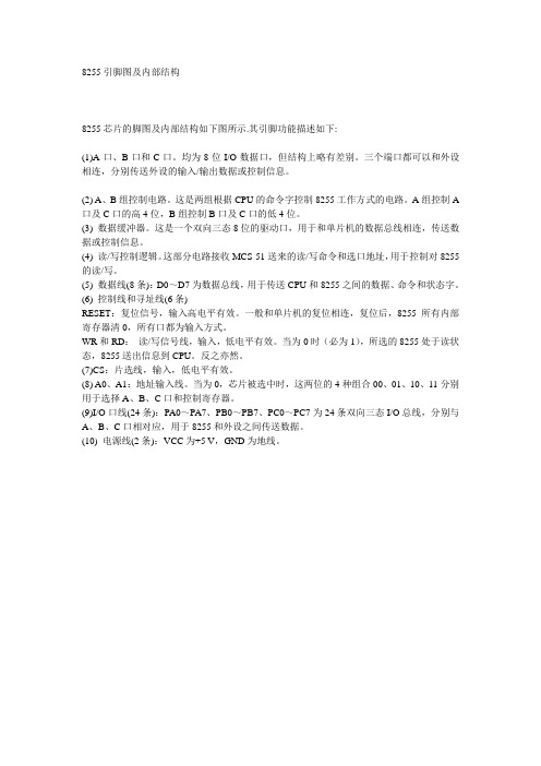
8255引脚图及内部结构8255芯片的脚图及内部结构如下图所示.其引脚功能描述如下:(1)A口、B口和C口。
均为8位I/O数据口,但结构上略有差别。
三个端口都可以和外设相连,分别传送外设的输入/输出数据或控制信息。
(2) A、B组控制电路。
这是两组根据CPU的命令字控制8255工作方式的电路。
A组控制A 口及C口的高4位,B组控制B口及C口的低4位。
(3) 数据缓冲器。
这是一个双向三态8位的驱动口,用于和单片机的数据总线相连,传送数据或控制信息。
(4) 读/写控制逻辑。
这部分电路接收MCS-51送来的读/写命令和选口地址,用于控制对8255的读/写。
(5) 数据线(8条):D0~D7为数据总线,用于传送CPU和8255之间的数据、命令和状态字。
(6) 控制线和寻址线(6条)RESET:复位信号,输入高电平有效。
一般和单片机的复位相连,复位后,8255所有内部寄存器清0,所有口都为输入方式。
WR和RD:读/写信号线,输入,低电平有效。
当为0时(必为1),所选的8255处于读状态,8255送出信息到CPU。
反之亦然。
(7)CS:片选线,输入,低电平有效。
(8) A0、A1:地址输入线。
当为0,芯片被选中时,这两位的4种组合00、01、10、11分别用于选择A、B、C口和控制寄存器。
(9)I/O口线(24条):PA0~PA7、PB0~PB7、PC0~PC7为24条双向三态I/O总线,分别与A、B、C口相对应,用于8255和外设之间传送数据。
(10) 电源线(2条):VCC为+5 V,GND为地线。
82559ER资料
GD82559ER Fast Ethernet**PCI ControllerNetworking SiliconDatasheetProduct Featuress Optimum Integration for Lowest CostSolution—Integrated IEEE 802.3 10BASE-T and100BASE-TX compatible PHY—Glueless 32-bit PCI master interface—128 Kbyte Flash interface—Thin BGA 15mm 2 package—ACPI and PCI Power Management—Power management event on“interesting” packets and link statuschange support—Test Access Port s High Performance Networking Functions —Chained memory structure similar to the 82559,82558, 82557, and 82596—Improved dynamic transmit chaining with multiple priorities transmit queues —Full Duplex support at both 10 and 100 Mbps —IEEE 802.3u Auto-Negotiation support —3 Kbyte transmit and 3 Kbyte receive FIFOs —Fast back-to-back transmission support with minimum interframe spacing—IEEE 802.3x 100BASE-TX FlowControl support—Low Power Features—Low power 3.3 V device—Efficient dynamic standby mode—Deep power down support—Clockrun protocol supportDocument Number: 714682-001Revision 1.0March 1999GD82559ER - Networking SiliconInformation in this document is provided in connection with Intel products. No license, express or implied, by estoppel or otherwise, to any intellectual property rights is granted by this document. Except as provided in Intel's T erms and Conditions of Sale for such products, Intel assumes no liability whatsoever, and Intel disclaims any express or implied warranty, relating to sale and/or use of Intel products including liability or warranties relating to fitness for a particular purpose, merchantability, or infringement of any patent, copyright or other intellectual property right. Intel products are not intended for use in medical, life saving, or life sustaining applications.Intel may make changes to specifications and product descriptions at any time, without notice.Designers must not rely on the absence or characteristics of any features or instructions marked "reserved" or "undefined." Intel reserves these for future definition and shall have no responsibility whatsoever for conflicts or incompatibilities arising from future changes to them.The 82559 may contain design defects or errors known as errata which may cause the product to deviate from published specifications. Current characterized errata are available on request.Contact your local Intel sales office or your distributor to obtain the latest specifications and before placing your product order.Copyright © Intel Corporation, 1999* Alert on LAN is a result of the Intel-IBM Advanced Manageability Alliance and a trademark of IBM.** Third-party brands and names are the property of their respective owners.Revision History RevisionDateRevision Description Mar. 1999 1.0First release.Networking Silicon — GD82559ERContents1.INTRODUCTION (1)1.1GD82559ER Overview (1)1.2Suggested Reading (1)2.GD82559ER ARCHITECTURAL OVERVIEW (3)2.1Parallel Subsystem Overview (3)2.2FIFO Subsystem Overview (4)2.310/100 Mbps Serial CSMA/CD Unit Overview (5)2.410/100 Mbps Physical Layer Unit (5)3.SIGNAL DESCRIPTIONS (7)3.1Signal Type Definitions (7)3.2PCI Bus Interface Signals (7)3.2.1Address and Data Signals (7)3.2.2Interface Control Signals (8)3.2.3System and Power Management Signals (9)3.3Local Memory Interface Signals (9)3.4Testability Port Signals (10)3.5PHY Signals (11)4.GD82559ER MEDIA ACCESS CONTROL FUNCTIONAL DESCRIPTION (13)4.182559ER Initialization (13)4.1.1Initialization Effects on 82559ER Units (13)4.2PCI Interface (14)4.2.182559ER Bus Operations (14)4.2.2Clockrun Signal (22)4.2.3Power Management Event Signal (22)4.2.4Power States (23)4.2.5Wake-up Events (27)4.3Parallel Flash Interface (28)4.4Serial EEPROM Interface (28)4.510/100 Mbps CSMA/CD Unit (30)4.5.1Full Duplex (31)4.5.2Flow Control (31)4.5.3Address Filtering Modifications (31)4.5.4Long Frame Reception (31)4.6Media Independent Interface (MII) Management Interface (32)5.GD82559ER TEST PORT FUNCTIONALITY (33)5.1Introduction (33)5.2Asynchronous Test Mode (33)5.3Test Function Description (33)5.485/85 (33)5.5TriState (34)5.6Nand - Tree (34)6.GD82559ER PHYSICAL LAYER FUNCTIONAL DESCRIPTION (37)6.1100BASE-TX PHY Unit (37)6.1.1100BASE-TX Transmit Clock Generation (37)GD82559ER — Networking Silicon6.1.2100BASE-TX Transmit Blocks (37)6.1.3100BASE-TX Receive Blocks (40)6.1.4100BASE-TX Collision Detection (41)6.1.5100BASE-TX Link Integrity and Auto-Negotiation Solution (41)6.1.6Auto 10/100 Mbps Speed Selection (41)6.210BASE-T Functionality (41)6.2.110BASE-T Transmit Clock Generation (41)6.2.210BASE-T Transmit Blocks (42)6.2.310BASE-T Receive Blocks (42)6.2.410BASE-T Collision Detection (43)6.2.510BASE-T Link Integrity (43)6.2.610BASE-T Jabber Control Function (43)6.2.710BASE-T Full Duplex (43)6.3Auto-Negotiation Functionality (43)6.3.1Description (44)6.3.2Parallel Detect and Auto-Negotiation (44)6.4LED Description (45)7.PCI CONFIGURATION REGISTERS (47)7.1LAN (Ethernet) PCI Configuration Space (47)7.1.1PCI Vendor ID and Device ID Registers (47)7.1.2PCI Command Register (48)7.1.3PCI Status Register (49)7.1.4PCI Revision ID Register (50)7.1.5PCI Class Code Register (50)7.1.6PCI Cache Line Size Register (50)7.1.7PCI Latency Timer (51)7.1.8PCI Header Type (51)7.1.9PCI Base Address Registers (51)7.1.10PCI Subsystem Vendor ID and Subsystem ID Registers (53)7.1.11Capability Pointer (53)7.1.12Interrupt Line Register (53)7.1.13Interrupt Pin Register (54)7.1.14Minimum Grant Register (54)7.1.15Maximum Latency Register (54)7.1.16Capability ID Register (54)7.1.17Next Item Pointer (54)7.1.18Power Management Capabilities Register (54)7.1.19Power Management Control/Status Register (PMCSR) (55)7.1.20Data Register (56)8.CONTROL/STATUS REGISTERS (57)8.1LAN (Ethernet) Control/Status Registers (57)8.1.1System Control Block Status Word (58)8.1.2System Control Block Command Word (59)8.1.3System Control Block General Pointer (59)8.1.4PORT (59)8.1.5Flash Control Register (59)8.1.6EEPROM Control Register (59)8.1.7Management Data Interface Control Register (59)8.1.8Receive Direct Memory Access Byte Count (60)8.1.9Early Receive Interrupt (60)Networking Silicon — GD82559ER8.1.10Flow Control Register (60)8.1.11Power Management Driver Register (60)8.1.12General Control Register (61)8.1.13General Status Register (61)8.2Statistical Counters (62)9.PHY UNIT REGISTERS (65)9.1MDI Registers 0 - 7 (65)9.1.1Register 0: Control Register Bit Definitions (65)9.1.2Register 1: Status Register Bit Definitions (66)9.1.3Register 2: PHY Identifier Register Bit Definitions (67)9.1.4Register 3: PHY Identifier Register Bit Definitions (67)9.1.5Register 4: Auto-Negotiation Advertisement Register Bit Definitions (67)9.1.6Register 5: Auto-Negotiation Link Partner Ability Register Bit Definitions (67)9.1.7Register 6: Auto-Negotiation Expansion Register Bit Definitions (68)9.2MDI Registers 8 - 15 (68)9.3MDI Register 16 - 31 (68)9.3.1Register 16: PHY Unit Status and Control Register Bit Definitions (68)9.3.2Register 17: PHY Unit Special Control Bit Definitions (69)9.3.3Register 18: PHY Address Register (70)9.3.4Register 19: 100BASE-TX Receive False Carrier Counter Bit Definitions (70)9.3.5Register 20: 100BASE-TX Receive Disconnect Counter Bit Definitions (70)9.3.6Register 21: 100BASE-TX Receive Error Frame Counter Bit Definitions (70)9.3.7Register 22: Receive Symbol Error Counter Bit Definitions (70)9.3.8Register 23: 100BASE-TX Receive Premature End of Frame Error CounterBit Definitions (71)9.3.9Register 24: 10BASE-T Receive End of Frame Error Counter Bit Definitions .719.3.10Register 25: 10BASE-T Transmit Jabber Detect Counter Bit Definitions (71)9.3.11Register 26: Equalizer Control and Status Bit Definitions (71)9.3.12Register 27: PHY Unit Special Control Bit Definitions (71)10.ELECTRICAL AND TIMING SPECIFICATIONS (73)10.1Absolute Maximum Ratings (73)10.2DC Specifications (73)10.3AC Specifications (76)10.4Timing Specifications (77)10.4.1Clocks Specifications (77)10.4.2Timing Parameters (78)12.PACKAGE AND PINOUT INFORMATION (85)12.1Package Information (85)12.2Pinout Information (86)12.2.1GD82559ER Pin Assignments (86)12.2.2GD82559ER Ball Grid Array Diagram (88)GD82559ER — Networking SiliconNetworking Silicon — GD82559ER 1.Introduction1.1GD82559ER OverviewThe 82559ER is part of Intel's second generation family of fully integrated 10BASE-T/100BASE-TX LAN solutions. The 82559ER consists of both the Media Access Controller (MAC) and thephysical layer (PHY) combined into a single component solution. 82559 family members build onthe basic functionality of the 82558 and contain power management enhancements.The 82559ER is a 32-bit PCI controller that features enhanced scatter-gather bus masteringcapabilities which enables the 82559ER to perform high-speed data transfers over the PCI bus.The82559ER bus master capabilities enable the component to process high-level commands andperform multiple operations, thereby off-loading communication tasks from the system CPU. Twolarge transmit and receive FIFOs of 3 Kbytes each help prevent data underruns and overruns,allowing the 82559ER to transmit data with minimum interframe spacing (IFS).The 82559ER can operate in either full duplex or half duplex mode. In full duplex mode the82559ER adheres to the IEEE 802.3x Flow Control specification. Half duplex performance isenhanced by a proprietary collision reduction mechanism.The 82559ER includes a simple PHY interface to the wire transformer at rates of 10BASE-T and100BASE-TX, and Auto-Negotiation capability for speed, duplex, and flow control. These featuresand others reduce cost, real estate, and design complexity.The 82559ER also includes an interface to a serial (4-pin) EEPROM and a parallel interface to a128 Kbyte Flash memory. The EEPROM provides power-on initialization for hardware andsoftware configuration parameters1.2Suggested ReadingThe 82559 family of devices are designed to be compliant with PC industry power managementinitiatives. This includes the ACPI, PCI Power Management Specification, Network Device Classspecification, etc. See the following publicaitons for more information about these topics.•PCI Specification, PCI Special Interest Group.•Network Device Class Reference, Revision 1.0, Intel Corporation, Microsoft Corporation, and Toshiba.•Advanced Configuration and Power Interface (ACPI) Specification, Intel Corporation, Microsoft Corporation, Toshiba.•Advanced Power Management (APM) Specification, Intel Corporation and MicrosoftCorporation.•82559 Fast Ethernet Multifunction PCI/CardBus Controller Datasheet, Intel Corporation.•LAN On Motherboard (LOM) Design Guide Application Note (AP-391), Intel Corporation.•Test Access Port Applications Note (AP-393), Intel Corporation.GD82559ER — Networking SiliconNetworking Silicon — GD82559ER2.GD82559ER Architectural OverviewFigure 1 is a high level block diagram of the 82559ER. It is divided into four main subsystems: a parallel subsystem, a FIFO subsystem, the 10/100 Mbps Carrier-Sense Multiple Access with Collision Detect (CSMA/CD) unit, and the 10/100 Mbps physical layer (PHY) unit.2.1Parallel Subsystem OverviewThe parallel subsystem is broken down into several functional blocks: a PCI bus master interface, a micromachine processing unit and its corresponding microcode ROM, and a PCI Target Control/Flash/EEPROM interface. The parallel subsystem also interfaces to the FIFO subsystem, passing data (such as transmit, receive, and configuration data) and command and status parameters between these two blocks.The PCI bus master interface provides a complete glueless interface to a PCI bus and is compliant with the PCI Bus Specification, Revision 2.2. The 82559ER provides 32 bits of addressing and data, as well as the complete control interface to operate on a PCI bus. As a PCI target, it follows the PCI configuration format which allows all accesses to the 82559ER to be automatically mapped into free memory and I/O space upon initialization of a PCI system. For processing of transmit and receive frames, the 82559ER operates as a master on the PCI bus, initiating zero wait state transfers for accessing these data parameters.The 82559ER Control/Status Register Block is part of the PCI target element. The Control/Status Register block consists of the following 82559ER internal control registers: System Control Block (SCB), PORT, Flash Control, EEPROM Control, and Management Data Interface (MDI) Control.The micromachine is an embedded processing unit contained in the 82559ER. The micromachine accesses the 82559ER microcode ROM working its way through the opcodes (or instructions) contained in the ROM to perform its functions. Parameters accessed from memory such as pointers to data buffers are also used by the micromachine during the processing of transmit or receive frames by the 82559ER. A typical micromachine function is to transfer a data buffer pointer field to the 82559ER DMA unit for direct access to the data buffer. The micromachine is divided into two units, Receive Unit and Command Unit which includes transmit functions. These two unitsFigure 1. 82559ER Block Diagram 10/100 Mbps CSMA/CD Data Interface Unit(DIU)100BASE-TX/10BASE-T PHY Four ChannelAddressing Unit -DMAPCI BusInterface Unit(BIU)PCI Target andFlash/EEPROMInterfaceMicro-machine Dual PortedFIFO 3 Kbyte Rx FIFOFIFO Control 3 Kbyte Tx FIFO Local MemoryInterfacePCI InterfaceTPE InterfaceGD82559ER — Networking Siliconoperate independently. Control is switched between the two units according to the microcodeinstruction flow. The independence of the Receive and Command units in the micromachine allowsthe 82559ER to interleave commands and receive incoming frames, with no real-time CPUintervention.The 82559ER contains an interface to an external Flash memory, and external serial EEPROM.These two interfaces are multiplexed. The Flash interface, which could also be used to connect toany standard 8-bit device, provides up to 128 Kbytes of addressing to the Flash. Both read andwrite accesses are supported. The Flash may be used for remote boot functions, network statisticaland diagnostics functions, and management functions. The Flash is mapped into host systemmemory (anywhere within the 32-bit memory address space) for software accesses. It is alsomapped into an available boot expansion ROM location during boot time of the system. Moreinformation on the Flash interface is detailed in Section 4.3, “Parallel Flash Interface” on page28.The EEPROM is used to store relevant information for a LAN connection such as node address, aswell as board manufacturing and configuration information. Both read and write accesses to theEEPROM are supported by the 82559ER. Information on the EEPROM interface is detailed inSection 4.4, “Serial EEPROM Interface” on page28.2.2FIFO Subsystem OverviewThe 82559ER FIFO subsystem consists of a 3 Kbyte transmit FIFO and 3 Kbyte receive FIFO.Each FIFO is unidirectional and independent of the other. The FIFO subsystem serves as theinterface between the 82559ER parallel side and the serial CSMA/CD unit. It provides a temporarybuffer storage area for frames as they are either being received or transmitted by the 82559ER,which improves performance:•Transmit frames can be queued within the transmit FIFO, allowing back-to-back transmission within the minimum Interframe Spacing (IFS).•The storage area in the FIFO allows the 82559ER to withstand long PCI bus latencies without losing incoming data or corrupting outgoing data.•The 82559ER transmit FIFO threshold allows the transmit start threshold to be tuned to eliminate underruns while concurrent transmits are being performed (i.e. pending transmitswill not be affected by the change in FIFO threshold).•The FIFO subsection allows extended PCI burst accesses with zero wait states to or from the 82559ER for both transmit and receive frames. This is because such the transfer is to the FIFOstorage area, rather than directly to the serial link.•Transmissions resulting in errors (collision detection or data underrun) are retransmitted directly from the 82559ER FIFO, therey increasing performance and eliminating the need tore-access this data from the host system.•Incoming runt receive frames (frames that are less than the legal minimum frame size) can be discarded automatically by the 82559ER without transferring this faulty data to the hostsystem, and without host intervention.•Bad Frames resolution can be selectively left to the 82559ER, or under software control.2.310/100 Mbps Serial CSMA/CD Unit OverviewThe CSMA/CD unit of the 82559ER allows it to be connected to either a 10 or 100 Mbps Ethernetnetwork. The CSMA/CD unit performs all of the functions of the 802.3 protocol such as frameformatting, frame stripping, collision handling, deferral to link traffic, etc. The CSMA/CD unit canalso be placed in a full-duplex mode, which allows simultaneous transmission and reception offrames.2.410/100 Mbps Physical Layer UnitThe Physical Layer (PHY) unit of the 82559ER allows connection to either a 10 or 100 MbpsEthernet network. The PHY unit supports Auto-Negotiation for 100BASE-TX Full Duplex,100BASE-TX Half Duplex, 10BASE-T Full Duplex, and 10BASE-T Half Duplex. It also supportsthree LED pins to indicate link status, network activity, and speed.The 82559ER does not supportexternal PHY devices and does not expose its internal MII bus.3.Signal Descriptions 3.1Signal Type Definitions 3.2PCI Bus Interface Signals 3.2.1Address and Data Signals Type Name Description IN Input The input pin is a standard input only signal.OUT Output The output pin is a Totem Pole Output pin and is a standard active driver.T/S Tri-State The tri-state pin is a bidirectional, input/output pin.S/T/S Sustained Tri-State The sustained tri-state pin is an active low tri-state signal owned and driven by one agent at a time. The agent asserting the S/T/S pin low must drive it high at least one clock cycle before floating the pin. A new agent can only assert an S/T/S signal low one clock cycle after it has been tri-stated by the previous owner.O/D Open Drain The open drain pin allows multiple devices to share this signal as a wired-OR.A/I Analog Input The analog input pin is used for analog input signals.A/O Analog Output The analog output pin is used for analog output signals.B Bias The bias pin is an input bias.Symbol Type Name and Function AD[31:0]T/S Address and Data. The address and data lines are multiplexed on the same PCI pins. A bus transaction consists of an address phase followed by one or more data phases. During the address phase, the address and data lines contain the 32-bit physical address. For I/O, this is a byte address; for configuration and memory, it is a Dword address. The 82559ER uses little-endian byte ordering (in other words, AD[31:24] contain the most significant byte and AD[7:0] contain the least significant byte). During the data phases, the address and data lines contain data.C/BE[3:0]#T/S Command and Byte Enable. The bus command and byte enable signals are multiplexed on the same PCI pins. During the address phase, the C/BE# lines define the bus command. During the data phase, the C/BE# lines are used as Byte Enables. The Byte Enables are valid for the entire data phase and determine which byte lanes carry meaningful data.PAR T/S Parity. Parity is even across AD[31:0] and C/BE[3:0]# lines. It is stable and valid one clock after the address phase. For data phases, PAR is stable and valid one clock after either IRDY# is asserted on a write transaction or TRDY# is asserted on a read transaction.Once PAR is valid, it remains valid until one clock after the completion of the current data phase. The master drives PAR for address and write data phases; and the target, for read data phases.3.2.2Interface Control Signals Symbol Type Name and Function FRAME#S/T/S Cycle Frame. The cycle frame signal is driven by the current master to indicate the beginning and duration of a transaction. FRAME# is asserted to indicate the start of a transaction and de-asserted during the final data phase.IRDY#S/T/S Initiator Ready. The initiator ready signal indicates the bus master’s ability to complete the current data phase and is used in conjunction with the target ready (TRDY#) signal. A data phase is completed on any clock cycle where both IRDY# and TRDY# are sampled asserted (low) simultaneously.TRDY#S/T/S Target Ready. The target ready signal indicates the selected device’s ability to complete the current data phase and is used in conjunction with the initiator ready (IRDY#) signal. A data phase is completed on any clock cycle where both IRDY# and TRDY# are sampled asserted (low) simultaneously.STOP#S/T/S Stop. The stop signal is driven by the target to indicate to the initiator that it wishes to stop the current transaction. As a bus slave, STOP# is driven by the 82559ER to inform the bus master to stop the current transaction. As a bus master, STOP# is received by the 82559ER to stop the current transaction.IDSEL IN Initialization Device Select. The initialization device select signal is used by the 82559ER as a chip select during PCI configuration read and write transactions. This signal is provided by the host in PCI systems.DEVSEL#S/T/S Device Select. The device select signal is asserted by the target once it has detected its address. As a bus master, the DEVSEL# is an input signal to the 82559ER indicating whether any device on the bus has been selected. As a bus slave, the 82559ER asserts DEVSEL# to indicate that it has decoded its address as the target of the current transaction.REQ#T/S Request. The request signal indicates to the bus arbiter that the 82559ER desires use of the bus. This is a point-to-point signal and every bus master has its own REQ#.GNT#IN Grant. The grant signal is asserted by the bus arbiter and indicates to the 82559ER that access to the bus has been granted. This is a point-to-point signal and every master has its own GNT#.INTA#O/D Interrupt A. The interrupt A signal is used to request an interrupt by the 82559ER. This is an active low, level triggered interrupt signal.SERR#O/D System Error. The system error signal is used to report address parity errors. When an error is detected, SERR# is driven low for a single PCI clock.PERR#S/T/S Parity Error. The parity error signal is used to report data parity errors during all PCI transactions except a Special Cycle. The parity error pin is asserted two clock cycles after the error was detected by the device receiving data. The minimum duration of PERR# is one clock for each data phase where an error is detected. A device cannot report a parity error until it has claimed the access by asserting DEVSEL# and completed a data phase.3.2.3System and Power Management Signals 3.3Local Memory Interface Signals Symbol Type Name and Function CLK IN Clock. The Clock signal provides the timing for all PCI transactions and is an input signal to every PCI device. The 82559ER requires a PCI Clock signal (frequency greater than or equal to 16 MHz) for nominal operation. The 82559ER supports Clock signal suspension using the Clockrun protocol.CLKRUN#IN/OUT O/D Clockrun. The Clockrun signal is used by the system to pause or slow down the PCI Clock signal. It is used by the 82559ER to enable or disable suspension of the PCI Clock signal or restart of the PCI clock. When the Clockrun signal is not used, this pin should be connected to an external pull-down resistor.RST#IN Reset. The PCI Reset signal is used to place PCI registers, sequencers, and signals into a consistent state. When RST# is asserted, all PCI output signals will be tri-stated.PME#O/D Power Management Event. The Power Management Event signal indicates that a power management event has occurred in a PCI bus system.ISOLATE#IN Isolate. The Isolate signal is used to isolate the 82559ER from the PCI bus. When Isolate is active (low), the 82559ER does not drive its PCI outputs (except PME#) or sample its PCI inputs (including CLK and RST#). If the 82559ER is not powered by an auxiliary power source, the ISOLATE# pin should be pulled high to the bus Vcc through a 4.7K-62K resistor.ALTRST#IN Alternate Reset. The Alternate Reset signal is used to reset the 82559ER on power-up. In systems that support an auxiliary power supply, ALTRST# should be connected to a power-up detection circuit. Otherwise, ALTRST# should be tied to V cc .VIO B IN Voltage Input/Output. The VIO pin is the a voltage bias pin for the PCI interface. This pin should be connected to 5V ± 5% in a 5 volt PCI system and 3.3 volts in a 3.3 volt PCI system. Be sure to install a 10K pull-up resistor. This resistor acts as a current limit resistor in system where the VIO bias voltage maybe shutdown. In this cases the 82559ER may consume additional current without a resistor.Symbol Type Name and Function FLD[7:0]T/S Flash Data Input/Output. These pins are used for Flash data interface.FLA[16]/CLK25OUT Flash Address[16]/25 MHz Clock. This multiplexed pin is controlled by the status of the Flash Address[7] (FLA[7]) pin. If FLA[7] is left floating, this pin is used as FLA[16]; otherwise, if FLA[7] is connected to a pull-up resistor, this pin is used as a 25 MHz clock.FLA[15]/EESK OUT Flash Address[15]/EEPROM Data Output. During Flash accesses, this multiplexed pin acts as the Flash Address [15] output signal. During EEPROM accesses, it acts as the serial shift clock output to the EEPROM.FLA[14]/EEDO IN/OUT Flash Address[14]/EEPROM Data Output. During Flash accesses, this multiplexed pin acts as the Flash Address [14] output signal. During EEPROM accesses, it acts as serial input data to the EEPROM Data Output signal.3.4Testability Port Signals FLA[13]/EEDI OUT Flash Address[13]/EEPROM Data Input. During Flash accesses, this multiplexed pin acts as the Flash Address [13] output signal. During EEPROM accesses, it acts as serial output data to theEEPROM Data Input signal.FLA[12:8]OUT Flash Address[12:8]. These pins are used as Flash address outputsto support 128 Kbyte Flash addressing.FLA[7]/CLKENB T/S Flash Address[7]/Clock Enable. This is a multiplexed pin and actsas the Flash Address[7] output signal during nominal operation. Whenthe PCI RST# signal is active, this pin acts as input control over theFLA[16]/CLK25 output signal. If the FLA[7]/CLKEN pin is connected toa pull-up resistor (3.3 K Ω), a 25 MHz clock signal is provided on theFLA[16]/CLK25 output; otherwise, it is used as FLA[16] output.FLA[6:2]OUT Flash Address[6:2]. These pins are used as Flash address outputsto support 128 Kbyte Flash addressing.FLA[1]/AUXPWR T/S Flash Address[1]/Auxiliary Power. This multiplexed pin acts as theFlash Address[1] output signal during nominal operation. When RST isactive (low), it acts as the power supply indicator. If the 82559ER is fedPCI power, this pin should be connected to a pull-down resistor; if the82559ER is fed by auxiliary power, this pin should be connected to apull-up resistor.FLA[0]T/S Flash Address [0]. This pin acts as the Flash Address[0] outputsignal during nominal operation.EECS OUT EEPROM Chip Select. The EEPROM Chip Select signal is used toassert chip select to the serial EEPROM.FLCS#OUT Flash Chip Select. The Flash Chip Select signal is active duringFlash.FLOE#OUT Flash Output Enable. This pin provides an active low output enablecontrol (read) to the Flash memory.FLWE#OUTFlash Write Enable. This pin provides an active low write enablecontrol to the Flash memory. SymbolType Name and Function SymbolType Name and Function TEST IN Test. If this input pin is high, the 82559ER will enable the test port. During nominal operation this pin should be connected to a pull-downresistor.TCK IN Testability Port Clock. This pin is used for the Testability Port Clocksignal.TI IN Testability Port Data Input. This pin is used for the Testability PortData Input signal.TEXEC IN Testability Port Execute Enable. This pin is used for the TestabilityPort Execute Enable signal.TO OUTTestability Port Data Output. This pin is used for the Testability PortData Output signal.。
分辩真假Intel82559服务器版网卡
如何分辩真假Intel(82559)服务器版网卡一、Intel 559服务器版介绍:Intel 559服务器版,采用intel 82559芯片,10/100M自适应,2000以上系统自带驱动(也有人说是WIN98以上自带驱动),支持windows linux novell等操作系统,有功能强大的Intel驱动软件包可以下载,这点比3com的网卡好一点,下个3com的网卡驱动还是比较困难的。
1、Intel 82559 特性如下:媒体:10Base-T/100Base-TX连接线:RJ-45总线:32位PCI支持的IEEE标准:802.3、802.3u、802.2、802.1p、802.1Q、802.1 GMRP符合标准:PCI 2.2、WfM 2.0、ACPI 1.0、RWU、PXE驱动程序支持:Windows 95/98/ME/NT/2000 - Linux、Netware、OS/2、Packet Driver 特点:内置6K快取、PROSet Utility、Boot Agent、DCREATE.EXE2、SERVER服务器版更有以下诸多先进特征:◆支持多种端口汇聚模式;◆使用Bus-mastering技术增大吞吐量及减少CPU占用率;◆支持热插拨(需要主板支持)更换网卡无需断电;◆支持多种标准网络管理模式,SNMP等等;其它诸多先进特性无法一一列举,请查看Intel官方网的介绍。
使用INTEL的PROSET就直接可以设置多张网卡组成一个虚拟网卡,实现负载均衡、链路冗余、FEC/802.3ad、GEC/802.ad、IEEE802.3ad等高级服务器网卡特征,是网吧、工程维护人员必备之利器!3、原装服务器版网卡对比桌面版几个好处:1、CPU占有率较桌面版的低,在大流量的时候表现更明显。
2、网络吞吐量比桌面版网卡大,而且错误率更低,这点经常上网下载APE、经常BT的朋友就有体验了。
3、使用intel proset软件就可以轻松支持双网卡或者多网卡捆绑工作了,捆绑之后可以实现冗余功能,也可以实现负载平衡和端口汇聚功能。
8255引脚图及引脚功能
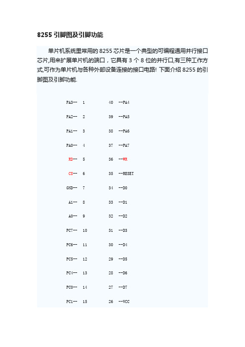
RD:读信号线,当这个输入引脚为低电平时,允许8255通过数据总线向CPU发送数据或状态信息,即CPU从8255读取信息或数据。
WR:写ቤተ መጻሕፍቲ ባይዱ信号,当这个输入引脚为低电平时,允许CPU将数据或控制字写8255。
D0~D7:三态双向数据总线,8255与CPU数据传送的通道,当CPU 执行输入输出指令时,通过它实现8位数据的读/写操作,控制字和状态信息也通过数据总线传送。
PA0~PA7:端口A输入输出线,一个8位的数据输出锁存器/缓冲器, 一个8位的数据输入锁存器。
PB0~PB7:端口B输入输出线,一个8位的I/O锁存器, 一个8位的输入输出缓冲器。
PC0~PC7:端口C输入输出线,一个8位的数据输出锁存器/缓冲器, 一个8位的数据输入缓冲器。端口C可以通过工作方式设定而分成2个4位的端口, 每个4位的端口包含一个4位的锁存器,分别与端口A和端口B配合使用,可作为控制信号输出或状态信号输入端口。
PC4--
13
28
--D6
PC0--
14
27
--D7
PC1--
15
26
--VCC
PC2--
16
25
--PB7
PC--
17
24
--PB6
PB0--
18
23
--PB5
PB1--
19
22
--PB4
PB2--
20
21
--PB3
8255引脚图
8255引脚功能说明:
RESET:复位输入线,当该输入端外于高电平时,所有内部寄存器(包括控制寄存器)均被清除,所有I/O口均被置成输入方式。
- 1、下载文档前请自行甄别文档内容的完整性,平台不提供额外的编辑、内容补充、找答案等附加服务。
- 2、"仅部分预览"的文档,不可在线预览部分如存在完整性等问题,可反馈申请退款(可完整预览的文档不适用该条件!)。
- 3、如文档侵犯您的权益,请联系客服反馈,我们会尽快为您处理(人工客服工作时间:9:00-18:30)。
82559ER Fast Ethernet PCI ControllerNetworking SiliconDatasheetProduct FeaturessOptimum Integration for Lowest Cost Solution —Integrated IEEE 802.3 10BASE-T and 100BASE-TX compatible PHY —Glueless 32-bit PCI master interface —128 Kbyte Flash interface —Thin BGA 15mm 2 package —ACPI and PCI Power Management —Power management event on “interesting” packets and link status change support —Test Access Port s Available in extended temperature version—Extended temperature range: -25 C to+85 C case temperature s High Performance Networking Functions —Chained memory structure similar to the 82559,82558, 82557, and 82596—Improved dynamic transmit chaining with multiple priorities transmit queues —Full Duplex support at both 10 and 100 Mbps —IEEE 802.3u Auto-Negotiation support —3 Kbyte transmit and 3 Kbyte receive FIFOs —Fast back-to-back transmission support with minimum interframe spacing —IEEE 802.3x 100BASE-TX Flow Control support —Low Power Features—Low power 3.3 V device—Efficient dynamic standby mode—Deep power down support—Clockrun protocol supportDocument Number: 714682-002Revision 1.382559ER - Networking SiliconInformation in this document is provided in connection with Intel products. No license, express or implied, by estoppel or otherwise, to any intellectual property rights is granted by this document. Except as provided in Intel's Terms and Conditions of Sale for such products, Intel assumes no liability whatsoever, and Intel disclaims any express or implied warranty, relating to sale and/or use of Intel products including liability or warranties relating to fitness for a particular purpose, merchantability, or infringement of any patent, copyright or other intellectual property right. Intel products are not intended for use in medical, life saving, or life sustaining applications.Intel may make changes to specifications and product descriptions at any time, without notice.Designers must not rely on the absence or characteristics of any features or instructions marked "reserved" or "undefined." Intel reserves these for future definition and shall have no responsibility whatsoever for conflicts or incompatibilities arising from future changes to them.The 82559 may contain design defects or errors known as errata which may cause the product to deviate from published specifications. Current characterized errata are available on request.Contact your local Intel sales office or your distributor to obtain the latest specifications and before placing your product order.Copyright © Intel Corporation, 1999* Alert on LAN is a result of the Intel-IBM Advanced Manageability Alliance and a trademark of IBM.Revision History RevisionDateRevision Description Mar. 19991.0First release.Mar. 20001.1Modified text description of Voltage Input/Output signal in Section 3.2.3, ”Sys-tem and Power Management Signals”.Mar. 2001 1.3Added information for the extended temperature version of the 82559ER sili-con.Networking Silicon — 82559ER Contents1.0Introduction (1)1.182559ER Overview (1)1.2Suggested Reading (1)2.082559ER Architectural Overview (3)2.1Parallel Subsystem Overview (3)2.2FIFO Subsystem Overview (4)2.310/100 Mbps Serial CSMA/CD Unit Overview (5)2.410/100 Mbps Physical Layer Unit (5)3.0Signal Descriptions (7)3.1Signal Type Definitions (7)3.2PCI Bus Interface Signals (7)3.2.1Address and Data Signals (7)3.2.2Interface Control Signals (8)3.2.3System and Power Management Signals (9)3.3Local Memory Interface Signals (10)3.4Testability Port Signals (10)3.5PHY Signals (12)4.082559ER Media Access Control Functional Description (13)4.182559ER Initialization (13)4.1.1Initialization Effects on 82559ER Units (13)4.2PCI Interface (14)4.2.182559ER Bus Operations (14)4.2.2Clockrun Signal (22)4.2.3Power Management Event Signal (22)4.2.4Power States (22)4.2.5Wake-up Events (27)4.3Parallel Flash Interface (28)4.4Serial EEPROM Interface (28)4.510/100 Mbps CSMA/CD Unit (30)4.5.1Full Duplex (31)4.5.2Flow Control (31)4.5.3Address Filtering Modifications (31)4.5.4Long Frame Reception (31)4.6Media Independent Interface (MII) Management Interface (32)5.082559ER Test Port Functionality (33)5.1Introduction (33)5.2Asynchronous Test Mode (33)5.3Test Function Description (33)5.485/85 (33)5.5Tristate (33)5.6Nand Tree (34)6.082559ER Physical Layer Functional Description (35)6.1100BASE-TX PHY Unit (35)82559ER — Networking Silicon6.1.1100BASE-TX Transmit Clock Generation (35)6.1.2100BASE-TX Transmit Blocks (35)6.1.3100BASE-TX Receive Blocks (38)6.1.4100BASE-TX Collision Detection (39)6.1.5100BASE-TX Link Integrity and Auto-Negotiation Solution (39)6.1.6Auto 10/100 Mbps Speed Selection (39)6.210BASE-T Functionality (39)6.2.110BASE-T Transmit Clock Generation (39)6.2.210BASE-T Transmit Blocks (40)6.2.310BASE-T Receive Blocks (40)6.2.410BASE-T Collision Detection (41)6.2.510BASE-T Link Integrity (41)6.2.610BASE-T Jabber Control Function (41)6.2.710BASE-T Full Duplex (41)6.3Auto-Negotiation Functionality (41)6.3.1Description (42)6.3.2Parallel Detect and Auto-Negotiation (42)6.4LED Description (43)7.0PCI Configuration Registers (45)7.1LAN (Ethernet) PCI Configuration Space (45)7.1.1PCI Vendor ID and Device ID Registers (45)7.1.2PCI Command Register (46)7.1.3PCI Status Register (47)7.1.4PCI Revision ID Register (48)7.1.5PCI Class Code Register (48)7.1.6PCI Cache Line Size Register (48)7.1.7PCI Latency Timer (49)7.1.8PCI Header Type (49)7.1.9PCI Base Address Registers (49)7.1.10PCI Subsystem Vendor ID and Subsystem ID Registers (51)7.1.11Capability Pointer (51)7.1.12Interrupt Line Register (51)7.1.13Interrupt Pin Register (52)7.1.14Minimum Grant Register (52)7.1.15Maximum Latency Register (52)7.1.16Capability ID Register (52)7.1.17Next Item Pointer (52)7.1.18Power Management Capabilities Register (52)7.1.19Power Management Control/Status Register (PMCSR) (53)7.1.20Data Register (54)8.0Control/Status Registers (55)8.1LAN (Ethernet) Control/Status Registers (55)8.1.1System Control Block Status Word (56)8.1.2System Control Block Command Word (57)8.1.3System Control Block General Pointer (57)8.1.4PORT (57)8.1.5Flash Control Register (57)8.1.6EEPROM Control Register (57)Networking Silicon — 82559ER8.1.7Management Data Interface Control Register (57)8.1.8Receive Direct Memory Access Byte Count (58)8.1.9Early Receive Interrupt (58)8.1.10Flow Control Register (58)8.1.11Power Management Driver Register (58)8.1.12General Control Register (59)8.1.13General Status Register (59)8.2Statistical Counters (60)9.0PHY Unit Registers (63)9.1MDI Registers 0 - 7 (63)9.1.1Register 0: Control Register Bit Definitions (63)9.1.2Register 1: Status Register Bit Definitions (64)9.1.3Register 2: PHY Identifier Register Bit Definitions (65)9.1.4Register 3: PHY Identifier Register Bit Definitions (65)9.1.5Register 4: Auto-Negotiation Advertisement Register Bit Definitions (65)9.1.6Register 5: Auto-Negotiation Link Partner Ability Register Bit Definitions .659.1.7Register 6: Auto-Negotiation Expansion Register Bit Definitions (66)9.2MDI Registers 8 - 15 (66)9.3MDI Register 16 - 31 (66)9.3.1Register 16: PHY Unit Status and Control Register Bit Definitions (66)9.3.2Register 17: PHY Unit Special Control Bit Definitions (67)9.3.3Register 18: PHY Address Register (68)9.3.4Register 19: 100BASE-TX Receive False Carrier Counter Bit Definitions689.3.5Register 20: 100BASE-TX Receive Disconnect Counter Bit Definitions ...689.3.6Register 21: 100BASE-TX Receive Error Frame Counter Bit Definitions .689.3.7Register 22: Receive Symbol Error Counter Bit Definitions (68)9.3.8Register 23: 100BASE-TX Receive Premature End of Frame ErrorCounter Bit Definitions 699.3.9Register 24: 10BASE-T Receive End of Frame Error Counter Bit Defini-tions 699.3.10Register 25: 10BASE-T Transmit Jabber Detect Counter Bit Definitions ..699.3.11Register 26: Equalizer Control and Status Bit Definitions (69)9.3.12Register 27: PHY Unit Special Control Bit Definitions (69)10.0Electrical and Timing Specifications (71)10.1Absolute Maximum Ratings (71)10.2DC Specifications (71)10.3AC Specifications (74)10.4Timing Specifications (75)10.4.1Clocks Specifications (75)10.4.2Timing Parameters (76)11.0Package and Pinout Information (83)11.1Package Information (83)11.2Pinout Information (84)11.2.182559ER Pin Assignments (84)11.2.282559ER Ball Grid Array Diagram (86)Networking Silicon — 82559ER Figures182559ER Block Diagram (3)2CSR I/O Read Cycle (15)3CSR I/O Write Cycle (15)4Flash Buffer Read Cycle (16)5Flash Buffer Write Cycle (17)6PCI Retry Cycle (18)7Memory Read Burst Cycle (19)8Memory Write Burst Cycle (19)9Isolate Signal Behavior to PCI Power Good Signal (26)1082559ER Initialization upon PCI RST# and ISOLATE# (27)1164 Word EEPROM Read Instruction Waveform (29)1282559ER EEPROM Format (29)13NRZ to MLT-3 Encoding Diagram (37)14Conceptual Transmit Differential Waveform (37)15Auto-Negotiation and Parallel Detect (43)16Two and Three LED Schematic Diagram (44)17PCI Configuration Registers (45)18PCI Command Register (46)19PCI Status Register (47)20Cache Line Size Register (48)21Base Address Register for Memory Mapping (49)22Base Address Register for I/O Mapping (50)2382559ER Control/Status Register (55)24RBIAS100 Resistance Versus Transmitter Current (73)25RBIAS10 Resistance Versus Transmitter Current (74)26PCI/CardBus Clock Waveform (75)27Output Timing Measurement Conditions (76)28Input Timing Measurement Conditions (76)29Flash Timings for a Read Cycle (79)30Flash Timings for a Write Cycle (79)31EEPROM Timings (80)3210BASE-T NLP Timings (81)33Auto-Negotiation FLP Timings (81)34Dimension Diagram for the 82559ER 196-Pin BGA (83)3582559ER Ball Grid Array Diagram (86)Note:This page left intentionally blank.Networking Silicon — 82559ER Tables1EEPROM Words Field Descriptions (30)24B/5B Encoder (35)3Magnetics Modules (37)4PCI Command Register Bits (46)5PCI Status Register Bits (47)682559ER ID Fields Programming (51)7Power Management Capability Register (52)8Power Management Control and Status Register (53)9Ethernet Data Register (54)10Power Management Driver Register (58)11General Control Register (59)12General Status Register (59)1382559ER Statistical Counters (60)14General DC Specifications (71)15PCI/CardBus Interface DC Specifications (71)16Flash/EEPROM Interface DC Specifications (72)17LED Voltage/Current Characteristics (72)18100BASE-TX Voltage/Current Characteristics (72)1910BASE-T Voltage/Current Characteristics (73)20AC Specifications for PCI Signaling (74)21PCI/CardBus Clock Specifications (75)22X1 Clock Specifications (75)23Measure and Test Condition Parameters (76)24PCI Timing Parameters (77)25Flash Timing Parameters (78)26EEPROM Timing Parameters (80)2710BASE-T NLP Timing Parameters (81)28Auto-Negotiation FLP Timing Parameters (81)29100Base-TX Transmitter AC Specification (82)3082559ER Pin Assignments (84)Note:This page left intentionally blank.1.0Introduction1.182559ER OverviewThe 82559ER is part of Intel's second generation family of fully integrated 10BASE-T/100BASE-TX LAN solutions. The 82559ER consists of both the Media Access Controller (MAC) and thephysical layer (PHY) combined into a single component solution. 82559 family members build onthe basic functionality of the 82558 and contain power management enhancements.The 82559ER is a 32-bit PCI controller that features enhanced scatter-gather bus masteringcapabilities which enables the 82559ER to perform high-speed data transfers over the PCI bus.The82559ER bus master capabilities enable the component to process high-level commands andperform multiple operations, thereby off-loading communication tasks from the system CPU. Twolarge transmit and receive FIFOs of 3 Kbytes each help prevent data underruns and overruns,allowing the 82559ER to transmit data with minimum interframe spacing (IFS).The 82559ER can operate in either full duplex or half duplex mode. In full duplex mode the82559ER adheres to the IEEE 802.3x Flow Control specification. Half duplex performance isenhanced by a proprietary collision reduction mechanism.The 82559ER includes a simple PHY interface to the wire transformer at rates of 10BASE-T and100BASE-TX, and Auto-Negotiation capability for speed, duplex, and flow control. These featuresand others reduce cost, real estate, and design complexity.The 82559ER also includes an interface to a serial (4-pin) EEPROM and a parallel interface to a128 Kbyte Flash memory. The EEPROM provides power-on initialization for hardware andsoftware configuration parameters1.2Suggested ReadingThe 82559 family of devices are designed to be compliant with PC industry power managementinitiatives. This includes the ACPI, PCI Power Management Specification, Network Device Classspecification, etc. See the following publications for more information about these topics.•PCI Specification, PCI Special Interest Group.•Network Device Class Reference, Revision 1.0, Intel Corporation, Microsoft Corporation, and Toshiba.•Advanced Configuration and Power Interface (ACPI) Specification, Intel Corporation, Microsoft Corporation, Toshiba.•Advanced Power Management (APM) Specification, Intel Corporation and MicrosoftCorporation.•82559 Fast Ethernet Multifunction PCI/CardBus Controller Datasheet, Intel Corporation.•LAN On Motherboard (LOM) Design Guide Application Note (AP-391), Intel Corporation.•Test Access Port Applications Note (AP-393), Intel Corporation.Note:This page left intentionally blank.2.082559ER Architectural OverviewFigure 1 is a high level block diagram of the 82559ER. It is divided into four main subsystems: a parallel subsystem, a FIFO subsystem, the 10/100 Mbps Carrier-Sense Multiple Access with Collision Detect (CSMA/CD) unit, and the 10/100 Mbps physical layer (PHY) unit.2.1Parallel Subsystem OverviewThe parallel subsystem is broken down into several functional blocks: a PCI bus master interface, a micromachine processing unit and its corresponding microcode ROM, and a PCI Target Control/Flash/EEPROM interface. The parallel subsystem also interfaces to the FIFO subsystem, passing data (such as transmit, receive, and configuration data) and command and status parameters between these two blocks.The PCI bus master interface provides a complete glueless interface to a PCI bus and is compliant with the PCI Bus Specification, Revision 2.2. The 82559ER provides 32 bits of addressing and data, as well as the complete control interface to operate on a PCI bus. As a PCI target, it follows the PCI configuration format which allows all accesses to the 82559ER to be automatically mapped into free memory and I/O space upon initialization of a PCI system. For processing of transmit and receive frames, the 82559ER operates as a master on the PCI bus, initiating zero wait state transfers for accessing these data parameters.The 82559ER Control/Status Register Block is part of the PCI target element. The Control/Status Register block consists of the following 82559ER internal control registers: System Control Block (SCB), PORT, Flash Control, EEPROM Control, and Management Data Interface (MDI) Control.The micromachine is an embedded processing unit contained in the 82559ER. The micromachine accesses the 82559ER microcode ROM working its way through the opcodes (or instructions) contained in the ROM to perform its functions. Parameters accessed from memory such as pointers to data buffers are also used by the micromachine during the processing of transmit or receive frames by the 82559ER. A typical micromachine function is to transfer a data buffer pointer field to the 82559ER DMA unit for direct access to the data buffer. The micromachine is divided into two units, Receive Unit and Command Unit which includes transmit functions. These two unitsFigure 1. 82559ER Block Diagram 10/100 Mbps CSMA/CDData Interface Unit(DIU)100BASE-TX/10BASE-T PHY Four ChannelAddressing Unit -DMAPCI Bus Interface Unit(BIU)PCI Target andFlash/EEPROMInterfaceMicro-machine Dual PortedFIFO 3 Kbyte Rx FIFOFIFO Control 3 Kbyte Tx FIFO Local MemoryInterfacePCIInterface T P E Interfaceoperate independently. Control is switched between the two units according to the microcodeinstruction flow. The independence of the Receive and Command units in the micromachine allowsthe 82559ER to interleave commands and receive incoming frames, with no real-time CPUintervention.The 82559ER contains an interface to an external Flash memory, and external serial EEPROM.These two interfaces are multiplexed. The Flash interface, which could also be used to connect toany standard 8-bit device, provides up to 128 Kbytes of addressing to the Flash. Both read andwrite accesses are supported. The Flash may be used for remote boot functions, network statisticaland diagnostics functions, and management functions. The Flash is mapped into host systemmemory (anywhere within the 32-bit memory address space) for software accesses. It is alsomapped into an available boot expansion ROM location during boot time of the system. Moreinformation on the Flash interface is detailed in Section 4.3, “Parallel Flash Interface”. TheEEPROM is used to store relevant information for a LAN connection such as node address, as wellas board manufacturing and configuration information. Both read and write accesses to theEEPROM are supported by the 82559ER. Information on the EEPROM interface is detailed inSection 4.4, “Serial EEPROM Interface”.2.2FIFO Subsystem OverviewThe 82559ER FIFO subsystem consists of a 3 Kbyte transmit FIFO and 3 Kbyte receive FIFO.Each FIFO is unidirectional and independent of the other. The FIFO subsystem serves as theinterface between the 82559ER parallel side and the serial CSMA/CD unit. It provides a temporarybuffer storage area for frames as they are either being received or transmitted by the 82559ER,which improves performance:•Transmit frames can be queued within the transmit FIFO, allowing back-to-back transmission within the minimum Interframe Spacing (IFS).•The storage area in the FIFO allows the 82559ER to withstand long PCI bus latencies without losing incoming data or corrupting outgoing data.•The 82559ER transmit FIFO threshold allows the transmit start threshold to be tuned to eliminate underruns while concurrent transmits are being performed (i.e. pending transmitswill not be affected by the change in FIFO threshold).•The FIFO subsection allows extended PCI burst accesses with zero wait states to or from the 82559ER for both transmit and receive frames. This is because such the transfer is to the FIFOstorage area, rather than directly to the serial link.•Transmissions resulting in errors (collision detection or data underrun) are retransmitted directly from the 82559ER FIFO, increasing performance and eliminating the need to re-access this data from the host system.•Incoming runt receive frames (frames that are less than the legal minimum frame size) can be discarded automatically by the 82559ER without transferring this faulty data to the hostsystem, and without host intervention.•Bad Frames resolution can be selectively left to the 82559ER, or under software control.2.310/100 Mbps Serial CSMA/CD Unit OverviewThe CSMA/CD unit of the 82559ER allows it to be connected to either a 10 or 100 Mbps Ethernetnetwork. The CSMA/CD unit performs all of the functions of the 802.3 protocol such as frameformatting, frame stripping, collision handling, deferral to link traffic, etc. The CSMA/CD unit canalso be placed in a full-duplex mode, which allows simultaneous transmission and reception offrames.2.410/100 Mbps Physical Layer UnitThe Physical Layer (PHY) unit of the 82559ER allows connection to either a 10 or 100 MbpsEthernet network. The PHY unit supports Auto-Negotiation for 100BASE-TX Full Duplex,100BASE-TX Half Duplex, 10BASE-T Full Duplex, and 10BASE-T Half Duplex. It also supportsthree LED pins to indicate link status, network activity, and speed.The 82559ER does not supportexternal PHY devices and does not expose its internal MII bus.Note:This page left intentionally blank.3.0Signal Descriptions 3.1Signal Type Definitions 3.2PCI Bus Interface Signals 3.2.1Address and Data Signals Type Name Description IN Input The input pin is a standard input only signal.OUT Output The output pin is a Totem Pole Output pin and is a standard active driver.T/S Tri-State The tri-state pin is a bidirectional, input/output pin.S/T/S Sustained Tri-State The sustained tri-state pin is an active low tri-state signal owned and driven by one agent at a time. The agent asserting the S/T/S pin low must drive it high at least one clock cycle before floating the pin. A new agent can only assert an S/T/S signal low one clock cycle after it has been tri-stated by the previous owner.O/D Open Drain The open drain pin allows multiple devices to share this signal as a wired-OR.A/I Analog Input The analog input pin is used for analog input signals.A/O Analog Output The analog output pin is used for analog output signals.B Bias The bias pin is an input bias.Symbol Type Name and Function AD[31:0]T/S Address and Data. The address and data lines are multiplexed on the same PCI pins. A bus transaction consists of an address phase followed by one or more data phases. During the address phase, the address and data lines contain the 32-bit physical address. For I/O, this is a byte address; for configuration and memory, it is a Dword address. The 82559ER uses little-endian byte ordering (in other words, AD[31:24] contain the most significant byte and AD[7:0] contain the least significant byte). During the data phases, the address and data lines contain data.C/BE[3:0]#T/S Command and Byte Enable. The bus command and byte enable signals are multiplexed on the same PCI pins. During the address phase, the C/BE# lines define the bus command. During the data phase, the C/BE# lines are used as Byte Enables. The Byte Enables are valid for the entire data phase and determine which byte lanes carry meaningful data.PAR T/S Parity. Parity is even across AD[31:0] and C/BE[3:0]# lines. It is stable and valid one clock after the address phase. For data phases, PAR is stable and valid one clock after either IRDY# is asserted on a write transaction or TRDY# is asserted on a read transaction.Once PAR is valid, it remains valid until one clock after the completion of the current data phase. The master drives PAR for address and write data phases; and the target, for read data phases.3.2.2Interface Control SignalsSymbol Type Name and FunctionFRAME#S/T/S Cycle Frame. The cycle frame signal is driven by the current master to indicate the beginning and duration of a transaction. FRAME# is asserted to indicate the start of a transaction and de-asserted during the final data phase.IRDY#S/T/S Initiator Ready. The initiator ready signal indicates the bus master’s ability to complete the current data phase and is used in conjunction with the target ready (TRDY#) signal. A data phase is completed on any clock cycle where both IRDY# and TRDY# are sampled asserted (low) simultaneously.TRDY#S/T/S Target Ready. The target ready signal indicates the selected device’s ability to complete the current data phase and is used in conjunction with the initiator ready (IRDY#) signal. A data phase is completed on any clock cycle where both IRDY# and TRDY# are sampled asserted (low) simultaneously.STOP#S/T/S Stop. The stop signal is driven by the target to indicate to the initiator that it wishes to stop the current transaction. As a bus slave, STOP# is driven by the 82559ER to inform the bus master to stop the current transaction. As a bus master, STOP# is received by the 82559ER to stop the current transaction.IDSEL IN Initialization Device Select. The initialization device select signal is used by the 82559ER as a chip select during PCI configuration read and write transactions. This signal is provided by the host in PCI systems.DEVSEL#S/T/S Device Select. The device select signal is asserted by the target once it has detected its address. As a bus master, the DEVSEL# is an input signal to the 82559ER indicating whether any device on the bus has been selected. As a bus slave, the 82559ER asserts DEVSEL# to indicate that it has decoded its address as the target of the current transaction.REQ#T/S Request. The request signal indicates to the bus arbiter that the 82559ER desires use of the bus. This is a point-to-point signal and every bus master has its own REQ#.GNT#IN Grant. The grant signal is asserted by the bus arbiter and indicates to the 82559ER that access to the bus has been granted. This is a point-to-point signal and every master has its own GNT#.INTA#O/D Interrupt A. The interrupt A signal is used to request an interrupt by the 82559ER. This is an active low, level triggered interrupt signal.SERR#O/D System Error. The system error signal is used to report address parity errors. When an error is detected, SERR# is driven low for a single PCI clock.PERR#S/T/S Parity Error. The parity error signal is used to report data parity errors during all PCI transactions except a Special Cycle. The parity error pin is asserted two clock cycles after the error was detected by the device receiving data. The minimum duration of PERR# is one clock for each data phase where an error is detected. A device cannot report a parity error until it has claimed the access by asserting DEVSEL# and completed a data phase.3.2.3System and Power Management SignalsSymbol Type Name and FunctionCLK IN Clock. The Clock signal provides the timing for all PCI transactions and is an input signal to every PCI device. The 82559ER requires a PCI Clock signal (frequency greater than or equal to 16 MHz) for nominal operation. The 82559ER supports Clock signal suspension using the Clockrun protocol.CLKRUN#IN/OUTO/DClockrun. The Clockrun signal is used by the system to pause or slowdown the PCI Clock signal. It is used by the 82559ER to enable ordisable suspension of the PCI Clock signal or restart of the PCI clock.When the Clockrun signal is not used, this pin should be connected toan external pull-down resistor.RST#IN Reset. The PCI Reset signal is used to place PCI registers, sequencers, and signals into a consistent state. When RST# is asserted, all PCI output signals will be tri-stated.PME#O/D Power Management Event. The Power Management Event signal indicates that a power management event has occurred in a PCI bus system.ISOLATE#IN Isolate. The Isolate signal is used to isolate the 82559ER from the PCI bus. When Isolate is active (low), the 82559ER does not drive its PCI outputs (except PME#) or sample its PCI inputs (including CLK and RST#). If the 82559ER is not powered by an auxiliary power source, the ISOLATE# pin should be pulled high to the bus Vcc through a 4.7K-62K resistor.ALTRST#IN Alternate Reset. The Alternate Reset signal is used to reset the 82559ER on power-up. In systems that support an auxiliary power supply, ALTRST# should be connected to a power-up detection circuit. Otherwise, ALTRST# should be tied to V cc.VIO BINVoltage Input/Output. The VIO pin is the voltage bias pin for the PCIinterface. In a 5 V or 3.3 V signaling environment, this pint should beconnected through a 100 KΩ resistor to the voltage supply (5 V or 3.3V, respectively). The resistor acts as a leakage current limiter insystems where the VIO bias voltage may be turned off.。