AD404M82RSB-5中文资料
OPA404KU,OPA404KP,OPA404KU 1K,OPA404KU 1KE4,OPA404KUG4,OPA404AG,OPA404BG, 规格书,Datasheet 资料
KP, KU Operating
KP, KU Storage
KP, KU θ Junction-Ambient
KP, KU
IO = 0mADC Ambient Temperature Ambient Temperature Ambient Temperature
© 1986 Burr-Brown Corporation
PDS-677F
Printed in U.S.A. August 1995
芯天下--/
SPECIFICATIONS
ELECTRICAL
At VCC = ±15VDC and TA = +25°C unless otherwise noted.
®
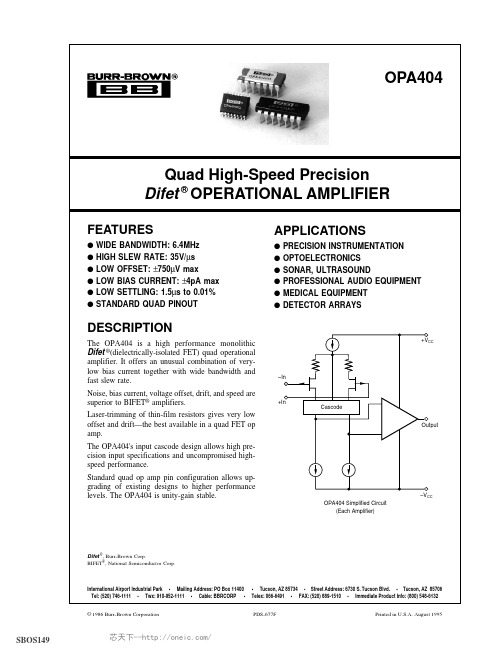
OPA404
2
芯天下--/
ELECTRICAL (FULL TEMPERATURE RANGE SPECIFICATIONS)
At VCC = ±15VDC and TA = TMIN to TMAX unless otherwise noted.
OPA404AG, KP, KU
8
0.5
12
1013 || 1 1014 || 3
±10.5 88 84
+13, –11 100 100
88
100
4
6.4
570
24
35
0.6
1.5
±11.5 +13.2, –13.8
±5
±10
80
1000
±10
±27
±40
±15
±5
±18
9
10
–25
BAS40-05中文资料
.30 (7.5) .12 (3)
.04 (1)
.08 (2) .04 (1) .08 (2)
.59 (15) .47 (12)
.03 (0.8)
0.2 (5)
.06 (1.5) .20 (5.1)
Dimensions in inches (millimeters)
Layout for RthJA test Thickness: Fiberglass 0.059 in (1.5 mm) Copper leads 0.012 in (0.3 mm)
1)
Value 40 2001) 6001) 2001) 150 –55 to +150
Unit V mA mA mW °C °C
VRRM IF IFSM Ptot Tj TS
Device on fiberglass substrate, see layout
4/98
元器件交易网
元器件交易网
BAS40 THRU BAS40-06
Schottky Diodes
SOT-23
.122 (3.1) .118 (3.0) .016 (0.4) 3
FEATURES ♦ These diodes feature very low turn-on
Top View
BAS40 THRU BAS40-06
ELECTRICAL CHARACTERISTICS
Ratings for one diode at 25 °C ambient temperature unless otherwise specified
Symbol Reverse Breakdown Voltage Tested with 10 µA Pulses Leakage Current Pulse Test tp < 300 µs at VR = 30 V Forward Voltage Pulse Test tp < 300 µs at IF = 1 mA at IF = 40 mA Capacitance at VR = 0 V, f = 1 MHz Reverse Recovery Time from IF = 10 mA through IR = 10 mA to IR = 1 mA Thermal Resistance Junction to Ambient Air
PG5404中文资料

PG5400 THRU PG5408GLASS PASSIVA TED JUNCTION PLASTIC RECTIFIER VOLTAGE - 50 to 1000 Volts CURRENT - 3.0 AmperesFEATURESl Plastic package has Underwriters Laboratory Flammability Classification 94V-O utilizing Flame Retardant Epoxy Molding Compoundl Glass passivated junction in DO-201AD packagel 3.0 ampere operation at T A =55¢J with no thermal runaway l Exceeds environmental standards of MIL-S-19500/228l Low reverse leakage current MECHANICAL DA TA Case: Molded plasticTerminals: Axial leads, solderable per MIL-STD-202, Method 208Mounting Position: Any Weight: 0.04 ounce, 1.1 gramMAXIMUM RA TINGS AND ELECTRICAL CHARACTERISTICS Ratings at 25¢J ambient temperature unless otherwise specified.Single phase, half wave, 60 Hz, resistive or inductive load.For capacitive load, derate current by 20%.PG5400PG5401PG5402PG5404PG5406PG5407PG5408UNITSMaximum Recurrent Peak Reverse Voltage501002004006008001000V Maximum RMS Voltage3570140280420560700V Maximum DC Blocking Voltage501002004006008001000V Maximum Average Forward Rectified Current .375"(9.5mm) lead length at T A =55¢J3.0APeak Forward Surge Current, 8.3ms single half sine-wave superimposed on rated load(JEDEC method)150A Maximum Forward Voltage at 3.0A1.2V Maximum Reverse Current at T a =25¢J At Rated DC Blocking Voltage T a =100¢J5.0100£g A £g A Typical Junction capacitance (Note 1)30P F Typical Thermal Resistance R £K JA(Note 2)20¢J /W Typical Reverse Recovery Time(Note 3)2£g S Operating and Storage T emperature Range T A-55 to +150¢JNOTES:1. Measured at 1 MHz and applied reverse voltage of 4.0 VDC2. Thermal resistance from junction to ambient and from junction to lead at 0.375”(9.5mm) lead length P.C.B mounted3. Reverse Recovery T est Conditions: I F =.5A, I R =1A, Irr=2.5ADO-201ADRATING AND CHARACTERISTIC CURVES PG5400 THRU PG5408PERCENT OF RATED PEAK REVERSE VOLTAGEAMBIENT TEMPERATURE, ¢JFig. 1-TYPICAL REVERSE CHARACTERISTICS Fig. 2-FORWARD DERATING CURVEAMBIENT TEMPERATURE, ¢JMAXIMUM FORWARD VOLTAGE-VFM(VpK)Fig. 3-FORWARD CURRENT DERATING CURVE Fig. 4-TYPICAL JUNCTION CAPACITANCENO. OF CYCLES AT 60HzFig. 5-MAXIMUM OVERLOAD SURGE CURRENT。
黑金 AN3845 RS232 485 422 通信模块用户手册说明书

第一部分RS232/485/422通信模块说明黑金AN3845模块专门为工业现场应用设计的RS232/485/422通信模块。
它包含一路RS232接口,2路RS485和2路RS422通信接口。
配合开发板实现RS232、485和422的数据远程传输和通信。
RS232、485和422接口分别采用MAX3232、MAX3485和MAX3490芯片作为电平转换芯片。
模块留有一个40针的排母用于连接开发板,RS232接口为一个标准的DB9串口公座,通过串口线直接连接电脑或者其他设备;RS485和RS422接口采用接线端子跟外部连接,超远距离传输可达上千米,另外RS485和RS422接口部分带有正负15KV的ESD 防护功能。
AN3845模块实物照片如下:AN3845通信模块正面图1.1 AN3485模块的参数说明以下为AN3485通信模块的详细参数:RS232接口●一路标准的DB9公座串行接口;●使用MAX3232作为RS232和TTL电平的转换;●传输率高达120Kbps数据通讯速率RS485接口●两路RS485接口,采用3线的接线端子;●使用MAX3485作为RS485和TTL的电平转换;●工业级设计,抗干扰能力超强,同时采用有效的防雷设计;●具有120欧匹配电阻,插上跳线帽即可使能匹配电阻,长距离传输时建议短接。
●支持多机通讯,允许接在最多128个设备的总线上●传输率高达500Kbps数据通讯速率。
RS422接口●两路RS422接口,采用5线的接线端子;●使用MAX3490作为RS422和TTL的电平转换;●工业级设计,抗干扰能力超强,同时采用有效的防雷设计;●具有120欧匹配电阻,插上跳线帽即可使能匹配电阻,长距离传输时建议短接。
●支持多机通讯,允许接在最多128个设备的总线上●传输率高达500Kbps数据通讯速率。
1.2 AN3485模块尺寸AN3485通信模块尺寸图第二部分模块功能说明2.1 RS232电路设计AN3485模块的RS232接口采用MAX3232芯片实现RS232和+3.3V TTL 电平的转换。
SD404中文资料

PRODUCT MARKING TO-92 SOT-89 SD4040B SD404
元器件交易网
SD404
CORPORATION
ABSOLUTE MAXIMUM RATINGS (TA = +25oC unless otherwise noted) Drain-Source Voltage . . . . . . . . . . . . . . . . . . . . . . . . . . . +20V Gate-Source Voltage . . . . . . . . . . . . . . . . . . . . . . . . . . . . -0.3V +20V Gate-Drain Voltage . . . . . . . . . . . . . . . . . . . . . . . . . . . . . -0.3V +20V Source-Drain Voltage . . . . . . . . . . . . . . . . . . . . . . . . . . . -0.3V Peak Pulsed Drain Current . . . . . . . . . . . . . . . . . . . . . . +0.8A Continuous Drain Current . . . . . . . . . . . . . . . . . . . . . . 100mA Power Dissipation (at or below TA = +25oC) . . . . . . . . 300mW Linear Derating Factor . . . . . . . . . . . . . . . . . . . . . . 3.0mW/ oC Operating Junction and Storage Temperature Range . . . . . . . . . . . . . . . . -55oC to +125oC
MBR4045中文资料
C, CAPACITANCE (pF)
1000
100
1
10 VR, REVERSE VOLTAGE (VOLTS)
100
110
120 130 140 TC, CASE TEMPERATURE (°C)
150
160
Figure 3. Typical Capacitance Per Leg
Figure 4. Current Derating Per Leg
TC = 25°C
TC = 100°C 1 100
TC = 25°C 800 0.01 0 10 20 30 VR, REVERSE VOLTAGE (VOLTS) 40 50
200 300 400 500 600 700 vF, INSTANTANEOUS FORWARD VOLTAGE (mV)
3
元器件交易网 MBR4045PT
Motorola reserves the right to make changes without further notice to any products herein. Motorola makes no warranty, representation or guarantee regarding the suitability of its products for any particular purpose, nor does Motorola assume any liability arising out of the application or use of any product or circuit, and specifically disclaims any and all liability, including without limitation consequential or incidental damages. “Typical” parameters which may be provided in Motorola data sheets and/or specifications can and do vary in different applications and actual performance may vary over time. All operating parameters, including “Typicals” must be validated for each customer application by customer’s technical experts. Motorola does not convey any license under its patent rights nor the rights of others. Motorola products are not designed, intended, or authorized for use as components in systems intended for surgical implant into the body, or other applications intended to support or sustain life, or for any other application in which the failure of the Motorola product could create a situation where personal injury or death may occur. Should Buyer purchase or use Motorola products for any such unintended or unauthorized application, Buyer shall indemnify and hold Motorola and its officers, employees, subsidiaries, affiliates, and distributors harmless against all claims, costs, damages, and expenses, and reasonable attorney fees arising out of, directly or indirectly, any claim of personal injury or death associated with such unintended or unauthorized use, even if such claim alleges that Motorola was negligent regarding the design or manufacture of the part. Motorola and are registered trademarks of Motorola, Inc. Motorola, Inc. is an Equal Opportunity/Affirmative Action Employer. Mfax is a trademark of Motorola, Inc. How to reach us: USA / EUROPE / Locations Not Listed: Motorola Literature Distribution; P.O. Box 5405, Denver, Colorado 80217. 1–303–675–2140 or 1–800–441–2447 Customer Focus Center: 1–800–521–6274 Mfax™: RMFAX0@ – TOUCHTONE 1–602–244–6609 ASIA/PACIFIC: Motorola Semiconductors H.K. Ltd.; 8B Tai Ping Industrial Park, Motorola Fax Back System – US & Canada ONLY 1–800–774–1848 51 Ting Kok Road, Tai Po, N.T., Hong Kong. 852–26629298 – /mfax/ HOME PAGE: /sps/ JAPAN: Nippon Motorola Ltd.: SPD, Strategic Planning Office, 4–32–1, Nishi–Gotanda, Shinagawa–ku, Tokyo 141, Japan. 81–3–5487–8488
莫萨 EDS-4012 系列 8+4G 连接口网管型 Ethernet 交换器说明书
EDS-4012系列8+4G 連接埠(提供8個802.3bt PoE 連接埠選項)網管型乙太網路交換器特色與優點•根據IEC 62443-4-1開發並符合IEC 62443-4-2工業網路安全標準•支援IEEE 802.3bt PoE ,各個連接埠的輸出功率高達90W•Turbo Ring 與Turbo Chain (對於250台交換器斷線復連時間小於20毫秒)1,以及透過RSTP/STP 協議支援網路備援•廣泛的電源輸入選項,可提供彈性部署•小巧彈性的外殼設計,適合狹窄的空間•支援MXstudio ,輕鬆實現可視化的工業網路管理認證簡介EDS-4012系列是一系列12埠網管型快速乙太網路交換器,可選擇4個1Gbps 光纖上行鏈路連接埠。
本系列也提供提供4個10/100BaseT (X)802.3af (PoE)、802.3at (PoE+)和802.3bt 相容乙太網路PoE 連接埠選項的型號,可選擇連接高頻寬PoE 裝置。
備援乙太網路技術如Turbo Ring 、Turbo Chain 和RSTP/STP ,將可增加系統的可靠性,並且改善網路骨幹的可用性。
EDS-4012系列專為應用需求所設計,如視訊與流程監控、ITS 和DCS 系統等,皆可從可擴充的網路骨幹中獲益。
EDS-4012系列符合IEC 62443-4-2和IEC 62443-4-1工業網路安全認證,涵蓋產品安全和安全開發生命週期要求,有助於我們的客戶滿足安全工業網路設計的合規要求。
規格Ethernet Interface10/100BaseT(X)Ports (RJ45connector)EDS-4012-4GS-LV/-HV/-T models:8EDS-4012-4GC-LV/-HV/-T models:8Auto negotiation speed Full/Half duplex modeAuto MDI/MDI-X connectionPoE Ports (10/100BaseT(X),RJ45connector)EDS-4012-8P-4GS-LVA/-LVB/-T models:8100/1000BaseSFP PortsEDS-4012-4GS-LV/-HV/-T models:4EDS-4012-8P-4GS-LVA/-VB/-T models:4Combo Ports (10/100/1000BaseT(X)or 100/1000BaseSFP)EDS-4012-4GC-LV/-HV/-T models:4StandardsIEEE 802.3for 10BaseTIEEE 802.3u for 100BaseT(X)and 100BaseFX IEEE 802.3ab for 1000BaseT(X)IEEE 802.3z for 1000BaseX IEEE 802.3x for flow controlIEEE 802.3ad for Port Trunk with LACP IEEE 802.1Q for VLAN TaggingIEEE 802.1D-2004for Spanning Tree Protocol IEEE 802.1w for Rapid Spanning Tree Protocol IEEE 802.1p for Class of Service IEEE 802.1X for authentication1.如果連接埠鏈路速度是1Gigabit 或更高,復原時間小於50毫秒Ethernet Software FeaturesFilter GMRP,GVRP,GARP,802.1Q VLAN,IGMP Snooping v1/v2/v3,IGMP Querier Management IPv4/IPv6,Flow control,Back Pressure Flow Control,DHCP Server/Client,ARP,RARP,LLDP,Port Mirror,Linkup Delay,SMTP,SNMP Trap,SNMP Inform,SNMPv1/v2c/v3,RMON,TFTP,SFTP,HTTP,HTTPS,Telnet,Syslog,Private MIBMIB P-BRIDGE MIB,Q-BRIDGE MIB,IEEE8021-SPANNING-TREE-MIB,IEEE8021-PAE-MIB,IEEE8023-LAG-MIB,LLDP-EXT-DOT1-MIB,LLDP-EXT-DOT3-MIB,SNMPv2-MIB,RMONMIB Groups1,2,3,9Redundancy Protocols STP,RSTP,Turbo Ring v2,Turbo Chain,Ring Coupling,Dual-Homing,Link Aggregation Security Broadcast storm protection,Rate Limit,Trust access control,Static Port Lock,MACSticky,HTTPS/SSL,SSH,RADIUS,TACACS+,Login and Password PolicyTime Management SNTP,NTP Server/Client,NTP AuthenticationProtocols IPv4/IPv6,TCP/IP,UDP,ICMP,ARP,RARP,TFTP,DNS,NTP Client,DHCP Server,DHCPClient,802.1X,QoS,HTTPS,HTTP,Telnet,SMTP,SNMPv1/v2c/v3,RMON,Syslog Switch PropertiesMAC Table Size16KJumbo Frame Size9.216KBMax.No.of VLANs256VLAN ID Range VID1to4094IGMP Groups512Priority Queues4Packet Buffer Size1MBLED InterfaceLED Indicators PWR1,PWR2,STATE,FAULT,MSTR/HEAD,CPLR/TAIL,SYNCSerial InterfaceConsole Port RS-232(TxD,RxD,GND),8-pin RJ45(115200,n,8,1)USB InterfaceUSB Connector USB Type A(Reserved)Input/Output InterfaceAlarm Contact Channels1,Relay output with current carrying capacity of1A@24VDCDigital Input Channels1Digital Inputs+13to+30V for state1-30to+3V for state0Max.input current:8mAButtons Reset buttonDIP Switch ConfigurationDIP Switches Turbo Ring,Master,Coupler,ReservePower ParametersConnection2removable4-contact terminal block(s)Pre-installed Power Module-LV/-LV-T models:PWR-100–LV-HV/-HV-T models:PWR-105-HV-I-LVA/-LVA-T models:PWR-101-LV-BP-I-LVB/-LVB-T models:PWR-103-LV-VB-INote The EDS-4012Series supports modular power supplies.The model names and powerparameters are determined by the installed power module.For example:EDS-4012-4GS-T+PWR-100–LV=EDS-4012-4GS-LV-TEDS-4012-4GS-T+PWR-105-HV-I=EDS-4012-4GS-HV-TIf you install a different power module,refer to the specifications of the correspondingmodel.For example,if you replace the power module of the EDS-4012-4GS–LV-Twith the PWR-105–HV-I,refer to the specifications of the EDS-4012–4GS-HV-T.Input Voltage-LV/-LV-T models:12/24/48VDC,Redundant dual inputs-HV/-HV-T models:110/220VDC/VAC,Single input-LVA/-LVA-T models:48VDC,Redundant dual inputs-LVB/-LVB-T models:12/24/48VDC,Redundant dual inputsOperating Voltage-LV/-LV-T models:9.6to60VDC-HV/-HV-T models:88to300VDC,85to264VAC-LVA/-LVA-T models:44to57VDC(>52VDC for PoE+output recommended)-LVB/-LVB-T models:12to57VDC(>52VDC for PoE+output recommended)Input Current-LV/-LV-T models:12-48VDC,1.50-0.40A or24VDC,0.70A-HV/-HV-T models:110-220VAC,50-60Hz,0.30-0.20A or110-220VDC,0.30-0.20A-LVA/-LVA-T models:48VDC,5.42A-LVB/-LVB-T models:12/48VDC,7.46/4.27A or24VDC,7.26APower Consumption(Max.)EDS-4012-4GS-LV/-T models:10.52WEDS-4012-4GS-HV-/T models:12.22WEDS-4012-4GC-LV/-T models:10.7WEDS-4012-4GC-HV/-T models:13.35WEDS-4012-8P-4GS-LVA/-T models:Without PoE:13.34WWith PoE:Max.240W for total PD power consumption@48VDC inputEDS-4012-8P-4GS-LVB/-T models:Without PoE:15.32WWith PoE:Max.180W for total PD power consumption@48VDC inputMax.150W for total PD power consumption@24VDC input(Max.120W for-T model)Max.62W for total PD consumption@12VDC inputMax.PoE Power Output per Port90WOverload Current Protection SupportedReverse Polarity Protection SupportedPhysical CharacteristicsIP Rating IP40Dimensions55x140x120mm(2.17x5.51x4.72in)Weight827g(1.82lb)Installation DIN-rail mounting,Wall mounting(with optional kit)Housing MetalEnvironmental LimitsOperating Temperature Standard Models:-10to60°C(14to140°F)Wide Temp.Models:-40to75°C(-40to167°F)Storage Temperature(package included)-40to85°C(-40to185°F)Ambient Relative Humidity5to95%(non-condensing)Standards and CertificationsIndustrial Cybersecurity IEC62443-4-1IEC62443-4-2Safety UL61010-2-201,EN62368-1(LVD)EMC EN55032/35,EN61000-6-2/-6-4EMI CISPR32,FCC Part15B Class AEMS IEC61000-4-2ESD:Contact:8kV;Air:15kVIEC61000-4-3RS:80MHz to1GHz:20V/mIEC61000-4-4EFT:Power:4kV;Signal:4kVIEC61000-4-5Surge:Power:4kV;Signal:4kVIEC61000-4-6CS:10VIEC61000-4-8PFMFVibration IEC60068-2-6Shock IEC60068-2-27Freefall IEC60068-2-32Railway EN50121-4Traffic Control NEMA TS2MTBFTime EDS-4012-4GC-LV/-T models:1,036,336hrsEDS-4012-4GC-HV/-T models:497,392hrsEDS-4012-4GS-LV/-T models:874,838hrsEDS-4012-4GS-HV/-T models:456,870hrsEDS-4012-8P-4GS-LVA/-T models:799,780hrsEDS-4012-8P-4GS-LVB/-T models:759,924hrsStandards Telcordia SR332WarrantyWarranty Period5yearsDetails See /tw/warrantyPackage ContentsDevice1x EDS-4012Series switchDocumentation1x quick installation guide1x product notice,Simplified Chinese1x product certificates of quality inspection,Simplified Chinese1x warranty card尺寸訂購資訊Model Name 10/100BaseT(X)Ports(RJ45Connector)PoE10/100BaseT(X)Ports(RJ45Connector)100/1000BaseSFPSlotsCombo Ports(10/100/1000BaseT(X)or100/1000BaseSFP)OperatingVoltagePre-installedPower ModuleOperatingTemp.EDS-4012-4GS-LV8–4–9.6to60VDC PWR-100-LV-10to60°C EDS-4012-4GS-LV-T8–4–9.6to60VDC PWR-100-LV-40to75°CEDS-4012-4GS-HV8–4–88to300VDC,85to264VACPWR-105-HV-I-10to60°CEDS-4012-4GS-HV-T8–4–88to300VDC,85to264VACPWR-105-HV-I-40to75°CEDS-4012-4GC-LV8––49.6to60VDC PWR-100-LV-10to60°C EDS-4012-4GC-LV-T8––49.6to60VDC PWR-100-LV-40to75°CEDS-4012-4GC-HV8––488to300VDC,85to264VACPWR-105-HV-I-10to60°CEDS-4012-4GC-HV-T8––488to300VDC,85to264VACPWR-105-HV-I-40to75°CEDS-4012-8P-4GS-LVA–84–44to57VDC(>52VDC for PoE+outputrecommended)PWR-101-LV-BP-I-10to60°CEDS-4012-8P-4GS-LVA-T –84–44to57VDC(>52VDC for PoE+outputrecommended)PWR-101-LV-BP-I-40to75°CEDS-4012-8P-4GS-LVB–84–12to57VDC(>52VDC for PoE+outputrecommended)PWR-103-LV-VB-I-10to60°CEDS-4012-8P-4GS-LVB-T –84–12to57VDC(>52VDC for PoE+outputrecommended)PWR-103-LV-VB-I-40to75°C配件(選購)SFP ModulesSFP-1GEZXLC SFP module with11000BaseEZX port with LC connector for110km transmission,0to60°C operatingtemperatureSFP-1GEZXLC-120SFP module with11000BaseEZX port with LC connector for120km transmission,0to60°C operatingtemperatureSFP-1GLHLC SFP module with11000BaseLH port with LC connector for30km transmission,0to60°C operatingtemperatureSFP-1GLHXLC SFP module with11000BaseLHX port with LC connector for40km transmission,0to60°C operatingtemperatureSFP-1GLSXLC SFP module with11000BaseLSX port with LC connector for1km/2km transmission,0to60°C operatingtemperatureSFP-1GLXLC SFP module with11000BaseLX port with LC connector for10km transmission,0to60°C operatingtemperatureSFP-1GSXLC SFP module with11000BaseSX port with LC connector for300m/550m transmission,0to60°Coperating temperatureSFP-1GZXLC SFP module with11000BaseZX port with LC connector for80km transmission,0to60°C operatingtemperatureSFP-1GLHLC-T SFP module with11000BaseLH port with LC connector for30km transmission,-40to85°C operatingtemperatureSFP-1GLHXLC-T SFP module with11000BaseLHX port with LC connector for40km transmission,-40to85°C operatingtemperatureSFP-1GLSXLC-T SFP module with11000BaseLSX port with LC connector for1km/2km transmission,-40to85°Coperating temperatureSFP-1GLXLC-T SFP module with11000BaseLX port with LC connector for10km transmission,-40to85°C operatingtemperatureSFP-1GSXLC-T SFP module with11000BaseSX port with LC connector for300m/550m transmission,-40to85°Coperating temperatureSFP-1GZXLC-T SFP module with11000BaseZX port with LC connector for80km transmission,-40to85°C operatingtemperatureSFP-1G10ALC WDM-type(BiDi)SFP module with11000BaseSFP port with LC connector for10km transmission;TX1310nm,RX1550nm,0to60°C operating temperatureSFP-1G10BLC WDM-type(BiDi)SFP module with11000BaseSFP port with LC connector for10km transmission;TX1550nm,RX1310nm,0to60°C operating temperatureSFP-1G20ALC WDM-type(BiDi)SFP module with11000BaseSFP port with LC connector for20km transmission;TX1310nm,RX1550nm,0to60°C operating temperatureSFP-1G20BLC WDM-type(BiDi)SFP module with11000BaseSFP port with LC connector for20km transmission;TX1550nm,RX1310nm,0to60°C operating temperatureSFP-1G40ALC WDM-type(BiDi)SFP module with11000BaseSFP port with LC connector for40km transmission;TX1310nm,RX1550nm,0to60°C operating temperatureSFP-1G40BLC WDM-type(BiDi)SFP module with11000BaseSFP port with LC connector for40km transmission;TX1550nm,RX1310nm,0to60°C operating temperatureSFP-1G10ALC-T WDM-type(BiDi)SFP module with11000BaseSFP port with LC connector for10km transmission;TX1310nm,RX1550nm,-40to85°C operating temperatureSFP-1G10BLC-T WDM-type(BiDi)SFP module with11000BaseSFP port with LC connector for10km transmission;TX1550nm,RX1310nm,-40to85°C operating temperatureSFP-1G20ALC-T WDM-type(BiDi)SFP module with11000BaseSFP port with LC connector for20km transmission;TX1310nm,RX1550nm,-40to85°C operating temperatureSFP-1G20BLC-T WDM-type(BiDi)SFP module with11000BaseSFP port with LC connector for20km transmission;TX1550nm,RX1310nm,-40to85°C operating temperatureSFP-1G40ALC-T WDM-type(BiDi)SFP module with11000BaseSFP port with LC connector for40km transmission;TX1310nm,RX1550nm,-40to85°C operating temperatureSFP-1G40BLC-T WDM-type(BiDi)SFP module with11000BaseSFP port with LC connector for40km transmission;TX1550nm,RX1310nm,-40to85°C operating temperatureSFP-1FELLC-T SFP module with1100Base single-mode with LC connector for80km transmission,-40to85°Coperating temperatureSFP-1FEMLC-T SFP module with1100Base multi-mode,LC connector for2/4km transmission,-40to85°C operatingtemperatureSFP-1FESLC-T SFP module with1100Base single-mode with LC connector for40km transmission,-40to85°Coperating temperaturePower SuppliesHDR-60-2460W/2.5A DIN-rail24VDC power supply,universal85to264VAC or120to370VDC input voltage,-30to70°C operating temperatureNDR-120-24120W/5.0A DIN-rail24VDC power supply,universal90to264VAC or127to370VDC input voltage,-20to70°C operating temperatureNDR-120-48120W/2.5A DIN-rail48VDC power supply,universal90to264VAC or127to370VDC input voltage,-20to70°C operating temperatureNDR-240-48240W/5.0A DIN-rail48VDC power supply,universal90to264VAC or127to370VDC input voltage,-20to70°C operating temperatureMDR-40-24DIN-rail24VDC power supply with40W/1.7A,85to264VAC,or120to370VDC input,-20to70°Coperating temperatureMDR-60-24DIN-rail24VDC power supply with60W/2.5A,85to264VAC,or120to370VDC input,-20to70°Coperating temperature©Moxa Inc.版權所有.2022年2月10日更新。
AD404M324VBB-5中文资料

ASCEND Semiconductor 4Mx4 EDO Data sheetDescriptionThe device CMOS Dynamic RAM organized as 4,194,304 words x 4 bits with extended data out access mode. It is fabricated with an advanced submicron CMOS technology and designed to operate from a single 3.3V oniy power supply. Low voltage operation is more suitable to be used on battery backup, portable elec-tronic application. lt is packaged in JEDEC standard 26/24-pin plastic SOJ or TSOP(II).Features• Single 3.3V(%) only power supply • High speed t RAC acess time: 50/60ns • Low power dissipation- Active mode : 432/396 mW (Mas) - Standby mode: 0.54 mW (Mas)• Extended - data - out(EDO) page mode access • I/O level: CMOS level (Vcc = 3.3V)• 2048 refresh cycle in 32 ms(Std.) or 128 ms(S-version)• 4 refresh modesh: - RAS only refresh- CAS - before - RAS refresh - Hidden refresh - Self-refresh(S-version)10±Pin Name FunctionA0-A10Address inputs- Row address - Column address - Refresh address DQ1~DQ4Data-in / data-out RAS Row address strobe CAS Column address strobe WE Write enable OE Output enable Vcc Power (+ 3.3V)VssGroundVCC 1DQ12DQ23DQ34DQ45VCC6891011 NC 12 WE 13A0 A117 A218 A319VSS RAS CAS OE A8A7A6A5A4VSSAD404M42VSPin Description Pin Configuration21222324 2526151416 A1026/24-PIN 300mil Plastic SOJA9VCC 1DQ12DQ23DQ34DQ45VCC6891011 NC 12 WE 13A0 A117 A218 A319VSS RAS CAS OE A8A7 A6A5 A4VSSAD404M42VT212223242526151416 A1026/24-PIN 300mil Plastic TSOP (ll)A9A0-A10A0-A10A0-A10WECASNO. 2 CLOCK GENERATORCOLUMN ADDRESS BUFFERS (11)REFRESH CONTROLLERREFRESH COUNTERBUFFERS (11)ADDRESS ROW NO. 1 CLOCK GENERATORA0RASA1A2A3A4A5A6A7A8CONTROLLOGICDATA-IN BUFFERDATA-OUT BUFFEROEDQ1.DQ4.COLUMN DECODER2048SENSE AMPLIFIERSI/O GATING2048x42048x2048x4MEMORY ARRAY2048R O W D E C O D E RVcc VssBlock DiagramA9A10TRUTH TABLENotes: 1. EARLY WRITE only.FUNCTIONRASCAS WE OE ADDRESSESDQ SNotesROW COL STANDBY H X X X X High-Z READL L H L ROW COL Data-Out WRITE: (EARLY WRITE )L L L X ROW COL Data-lnREAD WRITE L L ROW COL Data-Out,Data-ln EDO-PAGE-MODE READ1st Cycle L H L ROW COL Data-Out 2nd CycleL H L n/a COL Data-Out EDO-PAGE MODE WRITE1st CycleL L X ROW COL Data-In 2nd Cycle L L Xn/a COL Data-InEDO-PAGE-MODEREAD-WRITE 1st Cycle L ROW COL Data-Out, Data-In 2nd Cycle L n/a COL Data-Out, Data-In HIDDEN REFRESHREAD L H L ROW COL Data-Out WRITEL L X ROW COL Data-In 1RAS-ONLY REFRESH L H X X ROW n/a High-Z CBR REFRESHLHXXXHigh-ZH X →H L →L H →H L →H L →H L →H L →H L →H L →L H →H L →H L →L H→L H L →→L H L→→H L→Absolute Maximum RatingsRecommended DC Operating ConditionsCapacitanceTa = 25°C, V CC = 3.3V%, f = 1MHz Note: 1. Capacitance measured with effective capacitance measuring method. 2. RAS, CAS = V IH to disable Dout.ParameterSymbol Value Unit Voltage on any pin relative to Vss V T -0.5 to + 4.6V Supply voltage relative to Vss V CC -0.5 to + 4.6V Short circuit output current I OUT 50mA Power dissipation P D 1.0WOperating temperature T OPT 0 to + 70°C Storage temperatureT STG-55 to + 125°CParameter/Condition Symbol3.3 Volt VersionUnitMinTyp MaxSupply VoltageV CC 3.0 3.33.6V Input High Voltage, all inputs V IH 2.0-V CC + 0.3V Input Low Voltage, all inputsV IL-0.3-0.8VParameterSymbol Typ Max Unit Note Input capacitance (Address)C I1 -5pF 1Input capacitance (RAS, CAS, OE, WE)C I2-7pF 1Output capacitance(Data-in, Data-out)C I/O-7pF1, 210±DC Characteristics :(T a = 0 to 70°C, V CC = + 3.3V%, V SS = 0V)Parameter Symbol Test Conditions AD404M42V Unit Notes-5-6Min Max Min MaxOperating current I CC1RAS cyclingCAS, cyclingt RC = min-120-110mA1, 2Standby Current LowpowerS-versionI CC2LVTTL interfaceRAS, CAS = V IHDout = High-Z-0.5-0.5mACMOS interfaceRAS, -0.2VDout = High-Z-0.15-0.15mAStandardpowerversionLVTTL interfaceRAS, CAS = V IHDout = High-Z-2-2mACMOS interfaceRAS,-0.2VDout = High-Z-0.5-0.5mARAS- only refresh current I CC3RAS cycling, CAS = V IHt RC = min-120-110mA1, 2 EDO page mode current I CC4t PC = min-90-80mA1, 3CAS- before- RAS refresh current I CC5t RC = minRAS, CAS cycling-120-110mA1, 2Self- refresh current (S-Version)I CC8 - 550 - 55010±CAS V CC≥CAS V CC≥t RASS100µs≥µADC Characteristics :(T a = 0 to 70°C , V CC = +3.3V %, V SS = 0V)Notes:1. I CC is specified as an average current. It depends on output loading condition and cycle rate when the device is selected. I CC max is specified at the output open condition.2. Address can be changed once or less while RAS = V IL .3. For I CC4, address can be changed once or less within one EDO page mode cycle time.Parameter Symbol Test Conditions AD404M42VUnitNotes-5-6Min MaxMin MaxInput leakage current I LI + 0.3V -55-55Output leakage current I LO + 0.3V Dout = Disable -55-55Output high Voltage V OH I OH = -2mA 2.4- 2.4-V Output low voltage V OLI OL = +2mA-0.4-0.4V10±0V Vin V CC ≤≤µA 0V Vout V CC ≤≤µAAC Characteristics(T a = 0 to + 70°C , V cc = 3.3V %, V ss = 0V) *1, *2, *3, *4Test conditions• Output load: one TTL Load and 100pF (V CC = 3.3V %)• Input timing reference levels:V IH = 2.0V, V IL = 0.8V (V CC = 3.3V %)• Output timing reference levels:V OH = 2.0V, V OL = 0.8V10±10±10±Read, Write, Read- Modify- Write and Refresh Cycles (Common Parameters)ParameterSymbol AD404M42V UnitNotes-5-6Min MaxMin MaxRandom read or write cycle time t RC 84-104-ns RAS precharge timet RP 30-40-ns CAS precharge time in normal mode t CPN 10-10-ns RAS pulse width t RAS 50100006010000ns 5CAS pulse width t CAS 8100001010000ns 6Row address setup time t ASR 0-0-ns Row address hold time t RAH 8-10-ns Column address setup time t ASC 0-0-ns 7Column address hold time t CAH 8-10-ns RAS to CAS delay timet RCD 12371445ns 8RAS to column address delay time t RAD 10251230ns 9Column address to RAS lead time t RAL 25-30-ns RAS hold time t RSH 8-10-ns CAS hold timet CSH 38-40-ns CAS to RAS precharge time t CRP 5-5-ns 10OE to Din delay time t OED 12-15-ns Transition time (rise and fall)t T 150150ns 11Refresh periodt REF -32-32ms Refresh period (S- Version)t REF -128-128ms CAS to output in Low- Z t CLZ 0-0-ns CAS delay time from Din t DZC 0-0-ns OE delay time from Dint DZO-0-nsRead CycleWrite Cycle Parameter SymbolAD404M42V Unit Notes-5-6Min Max Min MaxAccess time from RAS t RAC-50-60ns12 Access time from CAS t CAC-14-15ns13, 14 Access time from column address t AA-25-30ns14, 15 Access time from OE t OEA-12-15nsRead command setup time t RCS0-0-ns7 Read command hold time to CAS t RCH0-0-ns10, 16 Read command hold time to RAS t RRH0-0-ns16 Output buffer turn-off time t OFF012015ns17 Output buffer turn-off time from OE t OEZ012015ns17Parameter SymbolAD404M42V Unit Notes -5-6Min Max Min MaxWrite command setup time t WCS0-0-ns7, 18 Write command hold time t WCH8-10-nsWrite command pulse width t WP8-10-nsWrite command to RAS lead time t RWL13-15-nsWrite command to CAS lead time t CWL8-10-nsData-in setup time t DS0-0-ns19 Data-in hold time t DH8-10-ns19 WE to Data-in delay t WED10-10-nsRead- Modify- Write CycleRefresh Cycle Parameter SymbolAD404M42V Unit Notes-5-6Min Max Min MaxRead-modify- write cycle time t RWC108-133-nsRAS to WE delay time t RWD64-77-ns18 CAS to WE dealy time t CWD26-32-ns18 Column address to WE delay time t AWD39-47-ns18 OE hold time from WE t OEH8-10-nsParameter SymbolAD404M42VUnit Notes -5-6Min Max Min MaxCAS setup time (CBR refresh) t CSR5-5-nsCAS hold time (CBR refresh)t CHR8-10-ns10 RAS precharge to CAS hold time t RPC5-5-ns7 RAS pulse width (self refresh)t RASS100-100-RAS precharge time (self refresh)t RPS90-110-nsCAS hold time (CBR self refresh)t CHS-50--50-nsWE setup time t WSR0-0-nsWE hold time t WHR10-10-nsµsEDO Page Mode CycleEDO Page Mode Read Modify Write CycleParameterSymbol AD404M42VUnit Notes-5-6Min MaxMin MaxEDO page mode cycle timet PC 20-25-ns EDO page mode CAS precharge time t CP 10-10-ns EDO page mode RAS pulse width t RASP 5010560105ns 20Access time from CAS precharge t CPA -30-35ns 10, 14RAS hold time from CAS precharge t CPRH 30-35-ns OE high hold time from CAS high t OEHC 5-5-ns OE high pulse widtht OEP 10-10-ns Data output hold time after CAS low t COH 5-5-ns Output disable delay from WEt WHZ 310310ns WE pulse width for output disable whenCAS hight WPZ7-7-nsParameterSymbol AD404M42V Unit Notes -5-6Min MaxMin MaxEDO page mode read- modify- write cycle CAS precharge to WE delay timet CPW 45-55-ns 10EDO page mode read- modify- write cycle timet PRWC56-68-nsNotes :1. AC measurements assume t T = 2ns.2. An initial pause of 100 is required after power up, and it followed by a minimum of eightinitialization cycles (RAS - only refresh cycle or CAS - before - RAS refresh cycle). If the internal refresh counter is used, a minimun of eight CAS - before - RAS refresh cycles are required.3. In delayed write or read-modify-write cycles, OE must disable output buffer prior to applying data to the device.4. All the V CC and V SS pins shall be supplied with the same voltages.5. t RAS (min) = t RWD (min)+t RWL (min)+t T in read-modify-write cycle.6. t CAS (min) = t CWD (min)+t CWL (min)+t T in read-modify-write cycle.7. t ASC (min), t RCS (min), t WCS (min), and t RPC are determined by the falling edge of CAS .8. t RCD (max) is specified as a reference point only, and t RAC (max) can be met with the t RCD (max) limit.Otherwise, t RAC is controlled exclusively by t CAC if t RCD is greater than the specified t RCD (max) limit. 9. t RAD (max) is specified as a reference point only, and t RAC (max) can be met with the t RAD (max) limit.Otherwise, t RAC is controlled exclusively by t AA if t RAD is greater than the specified t RAD (max) limit. 10. t CRP , t CHR , t RCH , t CPA and t CPW are determined by the rising edge of CAS .11. V IH (min) and V IL (max) are reference levels for measuring timing or input signals. Therefore, transitiontime is measured between V IH and V IL .12. Assumes that t RCD tRCD (max) and t RAD t RAD (max). If t RCD or t RAD is greater than the maximum recommended value shown in this table, t RAC exceeds the value shown. 13. Assumes that (max) and (max).14. Access time is determined by the maximum of t AA , t CAC , t CPA . 15. Assumes that (max) and (max). 16. Either t RCH or t RRH must be satisfied for a read cycle.17. t OFF (max) and t OEZ (max) define the time at which the output achieves the open circuit condition (highimpedance). t OFF is determined by the later rising edge of RAS or CAS.18. t WCS , t RWD , t CWD , and t AWD are not restrictive operating parameters. They are included in the datasheet as electrical characteristics only. If (min), the cycle is an early write cycle and the data out will remain open circuit (high impedance) throughout the entire cycle. If (min),(min), (min) and (min), the cycle is a read-modify-write and the data output will contain data read from the selected cell. If neither of the above sets of conditions is satisfied, the condition of the data output (at access time) is indeterminate.19. These parameters are referenced to CAS separately in an early write cycle and to WE edge in adelayed write or a read-modify-write cycle.20. t RASP defines RAS pulse width in EDO page mode cycles.µs ≤≤t RCD t RCD ≥t RADt RAD ≤t RCD t RCD ≤t RAD t RAD ≥t WCS t WCS ≥t RWD t RWD ≥t CWDt CWD ≥t AWD t AWD ≥t CPW t CPW≥Timing Waveforms• Read Cyclet RC t RASt RPtCRPtCPNtRRHtRCHt OEZ t OFF tOEA tCACt AAtRACt CLZD OUTtRCS t ASR tRAH tASC tCAH tRAD t RALtCAStRSH tRCDt TtCSHRASCASADDRESSWEDQ1~DQ4Note : = don’t care OEt OFFRowColumn= Invalid Dout•Early Write CycletRC t RASt RPt WCHt DSt DHt WCS t RALtCAStRSH tRCDt TtCSHRASCASWEDQ1~DQ4tCRPtASRtRAH tASCtCAH ADDRESSColumnRowtCPND INtRADt RAL• Delayed Write CycletRC t RASt RPt RWL t RCSt CAStRSH tRCDt TtCSHRASCAStASR tRAH tCAHADDRESSColumnRow tASC D INDQ1~DQ4WEtCRPtCPNt DHt DSt OEHt OEDOEt DSOPENt WPt CWL• Read - Modify - Write CycletRWC t RASt RPtRWDt WPtRADtRWL tCAStCWL tRCDt TtCPNRASCASWEtCRP t ASRtRAHtASCtCAHADDRESS Column RowDQ1~DQ4t DHt DSOEtRCStAWD tCWD D INt OEDt OEHt OEZt OEA t CAC t RACt AADQ1~DQ4D OUTOPENtDZCtDZO• EDO Page Mode Read CycletRASPtCPRHt RCStCAStRSH tRCDt OEAtCSHRASCAStASRtRAHtCAHADDRESStCASWEtCRPt CPOEDQ1~DQ4OPENtOEPD OUT 1t PCt CPtCAStCPNtCRPtRADtCAHtASCt ASCtCAHt ASCt RAL Row Column 1t OEAt OEHCtRRH tRCHt RACt AAt AAt AA t CPA t CPA t OEZt OFFt OFFt CACt OEZt CAC t CACt COHD OUT NWE OE Column 2Column N Rowt RPD OUT 2• EDO Page Mode Early Write CycletRASPtRPt WCSt CAStRSH tRCDRASCAStASRtRAHtCAHADDRESStCASWEt CPDQ1~DQ4t PCt CPt CAStCPNtCRP tCAH tASCtASC tCAH tASC Row Column 1t DS WE Column 2Column Nt WCH t WCS t WCH t WCS t WCHt DH t DS t DH t DS t DHD IN 1D IN 2D IN Nt TtCSH• EDO Page Mode Read-Early-Write Cyclet RASPtCPRHt RCStCAStRSH tRCDt OEAtCSHRASCAStASRtRAHtCAHADDRESStCASWEtCRPt CPOEDQ1~DQ4OPENtWEDt PCt CPtCAStCPNtCRPtRADtRAHtASCt ASCtCAHt ASCt RAL Row Column 1tWCStRCHt RACt AAt AAt CPA t DHt WHZt CACt CACt COHWE OE Column 2Column N Rowt RPt CAL tWCHDataDoutput 2Data Input NDataDoutput 1t DStCSH• EDO Page Mode Read-Modify-Write Cyclet RASPt CPRHt RCStCASt WP RASCASt ASRtRAHtCAHADDRESSt CASWEtRCDCPDQ1~DQ4tPRWCt CPtCAStCRPtRADtCAHtASCt ASCtCAH tASC Row Column 1tRWLtRCSt OEDt DZOt CAC WE OEt RPt RAL D OUT 2D OUT ND OUT 1tTt Column NColumn 2Column 1tRWD tAWD tCWDtCWLtRCStCWDtAWD tCPW tCWL tCPW tAWD tCWDtCWL t OEDt OEDt OEHt OEHt OEHt CAC t CAC t OEA t AAt RACt OEZt OEAt AA t CPAt OEZt OEAt AA t CPAt OEZ t DSt DHt WP t DSt DHt WP t DSt DHOPENOPENOPEN D IN 1D IN ND IN 2DQ1~DQ4t DZCt DZOt DZCt DZCt DZO• Read Cycle with WE Controlled Disablet WPZt RCStCAStRCDt TtCSHRASCASt ASRtRAHtCAHADDRESSColumnRow tASCD DQ1~DQ4WEt OEZt DSt WHZOEt RCH t OEA t CACt AAt RACt CLZOUTtRADRASADDRESSt RC t CRPt ASRt RAHt Tt RPCROWt OFFCAS t RASt RPOPENt CRPDQ1~DQ4RASt CSRt WSRt RPt T t RPCt OFFCAS t RASt RPOPENt CRPDQ1~DQ4t RPCt CHRt RASt RPt RCt RCt CHRt CSRt WHRt WSRt WHRWECAS-Before-RAS Refresh CycleRASWEt RPCt OFFt CSRt CHSt WSRCASt RASS t RPSOPENDQ1~DQ4t WHRHigh lmpedance• Hidden Refresh Cyclet RPt RASRASt RCDt CRPADDRESSWEt CHRt CASt RSHt RAHt ASRt ASCt CAHt RAL ROW t RCHt OEZCASDQ1~DQ4t Tt RCSD t RASt RASt RPt RPt RC t RCt RCt RADt RRHt OFF t OFFt OEA t CACt AAt RACCOlumnOUTOE(READ)(REFRESH)(REFRESH)Ordering informationAD404M42VSA-5• AD• Ascend Memory Product • 40 • Device Type• 4M4 • Density and Organization • 2• Refresh Rate, 2: 2K Refresh • V• T: 5V, V: 3.3V• S • Package Type (S : SOJ, T : TSOP II)• A• Version• 5• Speed (5: 50 ns, 6: 60 ns)Part Number Access time PackageAD404M42VSA-5AD404M42VSA-6AD404M42VTA-5AD404M42VTA-650 ns 60 ns 50 ns 60 ns300mil 26/24-Pin Plastic SOJTSOP IIPackaging information • 300 mil, 26/24-Pin Plastic SOJ• 300 mil, 26/24-Pin TSOP II。
施耐德Modicon M258可编程控制器产品目录
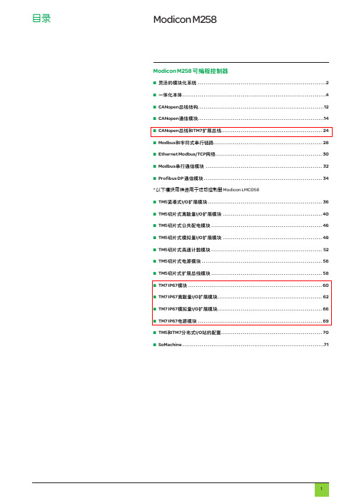
M258 可编程控制器都标配 4 路电压或电流模拟量输入 (12 位分辨率)。
<பைடு நூலகம்温度控制
此外还提供2、4或6通道以及12或16位不同分辨分辨率的扩展模块。 M258可编程控制器性能强大,能够连接多达200个模拟量I/O和/或温度模块,从而减
2
少了对设备需求的限制。
模拟量控制功能
< 速度控制
最多8通道高速 计数
软件组态
所有 M258
置和编程功能旨在降低成本和优化设备性能。
SoMachine 软件支持六种 IEC 61131-3 编程语言: v IL (指令表) v LD (梯形图) v SFC (顺序功能块) v ST (结构文本) v FBD (功能块图) v CFC (连续功能图)
另外还支持 PLCopen 功能块,以管理设备的运动控制和轴控制。
4个控制器状态ledrunmsbatteryapp0app16个内置通信端口状态ledethlaethstethnsusbhostmbscomcansts用于在5对称导轨上安装卸载的锁扣两个用于通信模块的pci闲置插槽带有可插拔接线端子和锁扣显示块和标签插槽的24电源模块io模块每个模块都具有带锁扣的可插拔接线端子显示io状态的显示块和标签夹持器插槽带上锁解锁功能的锁扣的可插拔接线端子在侧面用于连接下一个模块的总线扩展连接器rtc实时时钟电池插槽连接usb存储卡用于传输程序数据或固件更新的usba连接器标记为host用于连接编程计算机的usbb微型连接器标记为pgrport用于连接以太网和或magelisxbtgt图形终端的rj45连接器标记为ethernet用于连接rs232或rs485串行链路的rj45连接器标记为mbs9芯subd公头连接器标记为can0用于连接canopen总线仅限tm258lf42dt4ltm258lf42drtm258lf66dt4l1011
MA40404中文资料
V3.00 GaAs SchottkyMixer Diodes MA40400 SeriesFeaturesq Very Low Noise Figure from X through W-Bandq Low Junction Capacitanceq Low Series Resistanceq Wide Range of Available Product– Packaged Diodes– Chips– Beam Leads– Anti-Parallel Beam Leads– Bridge Quads– Ring Quads– Teesq Superior Dynamic Range to Silicon Diodesq Minimum Breakdown Voltage is 5 Voltsq Minimum 5 Gram Beam Strength For Beam LeadsDescriptionThis family of Gallium Arsenide Schottky diodes isfabricated with noble metal metallization and siliconnitride passivation to assure good reliability and lowseries resistance.These diodes are designed to give superior noise figurefrom X- through W-band. They are available in a widerange of packages, chip and beam lead configurations.The beam lead types include single beam leads, tees,anti-parallel pairs, ring and bridge quads.These diodes have lower series resistance than equivalentjunction capacitance silicon schottky diodes. This lowseries resistance results in superior conversion loss andnoise figure.The higher reverse voltage and low series resistance ofGallium Arsenide Bridge Quads make them particularlyattractive for use in AM modulation and/or sampling cir-cuits for signal processing and frequency generation.Case Styles2762721201191010元器件交易网V3.00Anti-Parallel Beam LeadsGaAs Schottky Mixer Diodes MA40400 SeriesAbsolute Maximum Ratings at 25°CSpecificationsTypical Characteristics Maximum 4I F 4Minimum 5Nominal 1, 3Series LO Test Noise Impedance Reverse Junction Resistance Model Case Frequency Figure Min./Max.Voltage Capacitance R S Min./Max.Number Style (GHz)NF (dB)(Ohms)V BCj (pF)(Ohms)MA4040311924 6.5250 / 50050.07 3 / 6MA4040411936 6.5250 / 50050.06 3 / 6MA4040712024 6.5250 / 50050.07 3 / 6MA4040812036 6.5250 / 50050.06 3 / 6MA4041127624 6.5250 / 50050.07 3 / 6MA40412276366.5250 / 50050.063 / 6Beam Leads and ChipsElectrical Specifications at 25°CPackaged Diodes元器件交易网V3.00GaAs Schottky Mixer Diodes MA40400 SeriesElectrical Specifications at 25°CBridge QuadRing QuadsTeesNotes:1.C j is measured at V R = 0V and f = 1.0 MHz.2.V F is measured at I F = 1.0 mA.3.Series Resistance, R s , is determined by subtracting the junction resistance Rj, from the measured value of 10 mA dynamic (slope)resistance, R T : R s = R T - Rj ohmsJunction resistance is computed from:Rj = 26/l F I F = 10 mAI F is the forward current in mA4.Noise figure measurements are single sideband noise figure with N IF =1.5 dB minimum. The noise figure of chips and beam lead types are performed on a sample of the lot. Chips are tested in a package. Beam leads are tested in a stripline holder The test conditions are as follows:LO Power 6.0 dBm LO Frequency 16.0 GHz24.0 GHz 35.0 GHzf if = 30 MHz R j= 22 Ohms5.V R is measured at l R = 10 µA.6.C j is measured at V R = 0V and f = 1.0 MHz. C j of anti-parallel diodes is comprised of the capacitance of two diode junctions in parallel.7.C j is measured between adjacent leads of device at V R = 0V and f = 1 MHz.8.C T = C j + C PC T is total capacitance C j is junction capacitance C P is packaged capacitance9.Conversion loss at 94 GHz with LO power ~ 8-12 dBm.10.The part number includes the case style as a suffix. i.e. MA40418 -1169 is a beam-lead Tee; MA40418-963 is the part in the case style 963.元器件交易网V3.00NOISE FIGURE vs LOCAL OSCILLATOR POWER(MA40400 SERIES)GaAs Schottky Mixer Diodes MA40400 SeriesTypical Performance CurvesDIODE CURRENT vs FORWARD VOLTAGE (MA40403 - 40412 PACKAGED G A A s CHIPS)DIODE CURRENT vs FORWARD VOLTAGE (MA40415, 40416 G A A s BEAM LEAD)I F IMPEDENCE vs LOCAL OSCILLATOR DRIVEWITH R L = 10 OHMS (MA40400 SERIES)LOCAL OSCILLATOR POWER in dBm元器件交易网元器件交易网GaAs Schottky Mixer Diodes MA40400 SeriesV3.00Case Styles(See appendix for complete styles)。
8205中文资料

U E D P R O D U C T R E F E R E N C E O N L Y Designed specifically to meet the requirement for extended opera-tion of battery-powered equipment such as cordless and cellular tele-phones, the A8205SLH voltage regulators offer the reduced dropout voltage and quiescent current essential for maximum battery life.Applicable also to palmtop computers and personal data assistants,these devices deliver a regulated output at up to 200 mA (transient),which is limited only by package power dissipation. Regulated output voltages of 2.7, 2.8, 3.0, 3.3, 3.6, 4.0, and 5.0 V are currently provided.Other voltages, down to 2.0 volts, are available on special order.A PMOS pass element provides a typical dropout voltage of only 75 mV at 100 mA of load current. The low dropout voltage permits deeper battery discharge before output regulation is lost. Quiescent current does not increase significantly as the dropout voltage is ap-proached, an ideal feature in standby/resume power systems where data integrity is crucial. Regulator accuracy and excellent temperature characteristics are provided by a bandgap reference. The A8205SLH includes an ENABLE input to give the designer complete control over power up, standby, or power down.These devices are supplied in a thermally enhanced 5-lead small-outline plastic package similar to the SOT-23, and fitting the SC-74A footprint. All devices are rated for operation over a temperature range of -20°C to +85°C.FEATURES AND BENEFITSI High Efficiency Provides Extended Battery Life I 75 mV Typical Dropout Voltage at I O = 100 mA I 55 µA Typical Quiescent Current Less Than 1 µA “Sleep” Current I Low Output NoiseI 200 mA Peak Output CurrentI Improved PSRR and Transient PerformanceAPPLICATIONSI Cordless and Cellular Telephones I Personal Data Assistants I Personal Communicators IPalmtop ComputersLOW-DROPOUT REGULATORS— HIGH EFFICIENCYData Sheet 27468.20Always order by complete part number, e.g., A8205SLH-xx , where “xx”is the required output voltage in tenths or “ADJ” for adjustable.8205PRELIMINARY INFORMATION(subject to change without notice)December 6, 19998205LOW-DROPOUTREGULATORS115 Northeast Cutoff, Box 15036Worcester, Massachusetts 01615-0036 (508) 853-5000Copyright © 1999, 2000 Allegro MicroSystems, Inc.A8205SLH Maximum Allowable Average Output Current* with device mounted on 2.24" x 2.24"(56.9 mm x 56.9 mm) solder-coated copper-clad board in still air.Allowable Total Average (10 ms) Output Current in Milliamperes with T J = 150°C, Duty Cycle = 100%†V I - V OT A 0.5 1.0 1.5 2.0 2.5 3.0 3.5 4.0* 4.5*25°C 20020020020020018916214212650°C 20020020020018215213011410170°C 200200200182145121104918185°C20020019714811898847466* Absolute maximum peak output current rating is 200 mA; absolute maximum input voltage is 7 V.† I O = (T J – T A )/([V I – V O ] R θJA x dc) = (150 – T A )/([V I – V O ] x 220 x 1.00)Output current rating can be increased (to 200 mA maximum) by additional heat sinking or reducing the duty cycle.8205LOW-DROPOUT REGULATORSELECTRICAL CHARACTERISTICS at T A = +25°C, V E = V I (unless otherwise noted).LimitsCharacteristic Symbol Test ConditionsMin.Typ.Max.UnitsOutput VoltageV O V I ≥ V O(nom) + 1 V, 1 mA ≤ I O ≤ 150 mA*,reference specified V O(nom)—0.0±1.5%Output Volt. Temp. Coeff.a VO V I = 6 V, I O = 10 mA, T J ≤ 125°C —40—ppm/°C Line Regulation ∆V O(∆VI)V O(nom) + 1 V ≤ V I ≤ 7 V, I O = 3 mA ——±1.5%Load Regulation∆V O(∆IO)V I = V O(nom) + 1 V, 1 mA ≤ I O ≤ 150 mA*——±1.5%V I = 7 V, 1 mA ≤ I O ≤ 150 mA*——±1.5%Dropout Voltage V I min - V OI O = 100 mA—75200mV Ground Terminal CurrentI GNDV I = V O(nom) + 1 V, I O = 1 mA —5565µA V I = V O(nom) + 1 V, I O = 150 mA*—5565µA V I = 7 V, I O = 1 mA —5565µA V I = 7 V, I O = 150 mA*—5565µA I QV I ≤ 7 V, V E ≤ 0.8 V, I O = 0 mA —— 1.0µA ENABLE Input VoltageV EH V I ≥ V O(nom) + 1 V, Output ON 2.0——V V ELV I ≥ V O(nom) + 1 V, Output OFF ——0.4V ENABLE Input Current I E V E = V I = 7 V——±1.0µA Internal Reference Voltage V REF — 1.26—V ADJUST Input Current I ADJ A8205SLH-ADJ only—0.10—µARejection RatioPSRRV I = V O(nom) + 1.5 V, V i = 100 mV,I O = 30 mA, f = 60 Hz—70—dB Output Noisee n10 Hz ≤ f ≤ 100 kHz, I O = 10 mA, C O = 10 µF —0.5—µV/√HzTypical values are at T A = +25°C and are given for circuit design information only.* Pulse test (≤20 ms). See previous page for duty cycle limitations.8205LOW-DROPOUTREGULATORS115 Northeast Cutoff, Box 15036Worcester, Massachusetts 01615-0036 (508) 853-5000APPLICATIONS INFORMATIONLinear regulators require input and output capacitors in order to maintain over-all loop stability. The recommended minimum value for the input capacitor is 0.1 µF. The output capacitor is the dominant pole that provides the high-frequency compensa-tion required for over-all regulator loop stability. These devices are stable with as little as 1 µF. However, to ensure stable operation under all conditions and capacitor types, the recom-mended minimum value is 4.7 µF. The output capacitor may be partially distributed through the load circuits. However, at least 1 µF should be connected at the regulator using the shortest and widest foil pattern possible.The A8205SLH-ADJ requires an external voltage divider to set up the desired regulated output voltage between 2.0 V and 6.8 V (V I ≤ 7 V). The two resistors are chosen such thatV O = 1.26 (R 1 + R 2)/R 2.The resistor values are usually as high as possible to maintain high circuit efficiency, but R 2 should be less than 300 k Ω.ENABLE(ACTIVE HIGH)INPUT (7.0 V MAX)Thermal ConsiderationsThese devices are intended to provide more than 150 mA of continuous current in a very small package. The table on page 2of this data sheet gives the maximum allowable average output current for a worst-case printed circuit design (R θJA = 220°C/W with a minimum footprint). Performance improvement is easily accomplished with the addition of 1 square inch of copper at terminal 2 (R θJA = 170°C/W).8205LOW-DROPOUTREGULATORSTHIS PAGE INTENTIONALLY LEFT BLANK8205LOW-DROPOUTREGULATORS115 Northeast Cutoff, Box 15036Worcester, Massachusetts 01615-0036 (508) 853-5000THIS PAGE INTENTIONALLY LEFT BLANK8205LOW-DROPOUT REGULATORSDimensions in Inches(for reference only)Dimensions in Millimeters(controlling dimensions)MINDwg. MA-011-5 mmNOTES: 1. Tolerances on package height and width represent allowable mold offsets.Dimensions given are measured at the widest point (parting line).2. Exact body and lead configuration at vendor’s option within limits shown.3. Height does not include mold gate flash.4. Where no tolerance is specified, dimension is nominal.MIN8205LOW-DROPOUTREGULATORS115 Northeast Cutoff, Box 15036Worcester, Massachusetts 01615-0036 (508) 853-5000The products described here are manufactured under one or more U.S. patents or U.S. patents pending.Allegro MicroSystems, Inc. reserves the right to make, from time to time, such departures from the detail specifications as may be required to permit improvements in the performance, reliability, ormanufacturability of its products. Before placing an order, the user is cautioned to verify that the information being relied upon is current.Allegro products are not authorized for use as critical components in life-support devices or systems without express written approval.The information included herein is believed to be accurate and reliable. However, Allegro MicroSystems, Inc. assumes no responsi-bility for its use; nor for any infringement of patents or other rights of third parties which may result from its use.。
MBR40250中文资料

TJ *65 to +150 °C
Voltage Rate of Change (Rated VR)
dv/dt
10,000 V/ms
Maximum ratings are those values beyond which device damage can occur. Maximum ratings applied to the device are individual stress limit values (not normal operating conditions) and are not valid simultaneously. If these limits are exceeded, device functional operation is not implied, damage may occur and reliability may be affected.
1. Pulse Test: Pulse Width = 300 ms, Duty Cycle ≤ 2.0%.
Symbol
RqJC RqJA
Value
2.0 60
Unit °C/W
Symbol
Value
Unit
VF
V
1.0
0.9
IR
mA
1.0
50
CT
500
pF
2
元器件交易网
INCHES
DIM MIN MAX A 0.570 0.620 B 0.380 0.405 C 0.160 0.190 D 0.025 0.035 F 0.142 0.147 G 0.095 0.105 H 0.110 0.155 J 0.018 0.025 K 0.500 0.562 L 0.045 0.060 N 0.190 0.210 Q 0.100 0.120 R 0.080 0.110 S 0.045 0.055 T 0.235 0.255 U 0.000 0.050 V 0.045 −−− Z −−− 0.080
4043门机技术规格书

4043门机技术规格书一、主要配套件表(单台)注:其他详见技术规格书附表。
二、技术规格书目录S1 起重机的使用地点S2 概述S3 选用标准和规定S4 当地条件和设计参数S5 起重机的稳定性S6 材料、部件及配套件S7 工艺S8 结构S9 机房S10 司机室S10-1 主要控制装置S10-2 辅助控制装置S10-3 仪表盘S10-4 座椅S10-5 窗户S10-6 空调和通风S10-7 司机室通道S10-8 墙壁、地板S10-9 司机室位置S10-10 其它S11 行走机构S12 防风及锚定装置S13 润滑S14 门架及转盘S15 回转支承及旋转机构S16 变幅机构S17 起升机构S18 四连杆机构S19 穿绳S20 人字架S21 平台、阶梯、通道和直梯S22 供电S23 主要电气设备、电路设计及PLC的应用S24 司机室供电S25 维修低压电源配电箱S26 故障显示和监视系统S27 限位开关、联锁开关S27-1 起升S27-2 变幅S27-3 行走S27-4 旋转S28 紧急停车按钮S29 指示灯S30 警报信号及避雷装置S31 风速指示器S32 布线S33 端子S34 通信扩音设备S35 照明S36 电源插座S37 吊钩、抓斗及防转装置S38 油漆及准备工作S39 标牌S40 工具附件及检测仪表S41 检验及试验文件S42 使用保养和修理手册S43 设计的确认S44 确认的图纸和文件S45 随机备件S46 附表S47 安装调试、运输和将起重机放置在买方码头轨道上的工作S48 测试和检验S49 复核试车和验收S50 竣工图纸和文件S51 竣工资料的整理S52 技术培训S53 交货时间及地点S1 起重机使用地点京唐港三十二号通用散货泊位。
S2 概述本起重机为安装在岸边轨道上,能够使用抓斗和吊钩作业的移动起重机,该机在吊钩及抓斗情况下,能吊起40T的重物(使用抓斗时应包含抓斗自重),其结构形式为四连杆起重臂,齿条变幅,可带载作水平变幅,可正反回转360°。
IXDN404PI中文资料

CL=1800pF Vcc=18V CL=1800pF Vcc=18V CL=1800pF Vcc=18V CL=1800pF Vcc=18V
VIN = 3.5V VIN = 0V VIN = + VCC
Specifications Subject To Change Without Notice
VCC + 0.3
V
IIN
Input current
0V ≤ VIN ≤ VCC
-10
10
µA
VOH VOL ROH
ROL
IPEAK
High output voltage
Low output voltage
Output resistance @ Output High Output resistance @ Output Low Peak output current
Package Type
8-Pin PDIP 8-Pin SOIC with Grounded Metal Back 8-Pin SOIC 16-Pin SOIC with Grounded Metal Back 16-Pin SOIC 8-Pin PDIP 8-Pin SOIC with Grounded Metal Back 8-Pin SOIC 16-Pin SOIC with Grounded Metal Back 16-Pin SOIC 8-Pin PDIP 8-Pin SOIC with Grounded Metal Back 8-Pin SOIC 16-Pin SOIC with Grounded Metal Back 16-Pin SOIC
Applications
AD9954芯片资料中文版
AD9954- Direct Digital Synthesizer400 MSPS 14-Bit, 1.8 V CMOS功能: (2)应用 (2)概述 (2)AD9954电气特性 (3)最大操作范围 (4)Table 2. (4)管脚定义 (4)管脚功能描述 (4)典型的性能特性 (6)原理 (7)器件块 (7)控制寄存器位描述 (10)Other Register Descriptions 其他寄存器描述 (14)Programming AD9954 Features-- AD9954编程特性 (18)SERIAL PORT OPERATION串口操作 (19)INSTRUCTION BYTE指令字节 (20)SERIAL INTERFACE PORT PIN DESCRIPTION串行接口管脚描述 (20)MSB/LSB TRANSFERS (20)RAM I/O VIA SERIAL PORT (21)Power-Down Functions of the AD9954 AD9954省电功能 (21)功能:400MSPS 内部时钟 集成14位DAC可编程相位/幅度抖动 32位控制字相位噪声小于等于-120dbc/Hz@1kHz(DAC 输出)出色的动态性能>80db SFDR@160MHz (偏离100KHz ) 串行I/O 口控制 超高速模拟比较器 自动线性和非线性扫频能力 4种频率/相位偏移坡面 1.8v 电压供电软件或者硬件控制休眠内部集成1024字节*32位RAM 大多数输入口支持5v 电平PLL REFCLK 乘法器(4倍-20倍) 单晶振驱动内部时钟 相位调制能力 多芯片同步 应用敏捷LO 频率输出 可编程的时钟发生器雷达和扫频系统中的FM 啁啾源自动雷达测试和测量设备 声光设备驱动概述AD9954具有一个14位DAC 最高达400 MSPS 的DDS 。
AD9954使用了先进的DDS 技术,内部集成高速,高性能的DAC 形成数字可编程,完整的高频合成器,能产生高达200MHz 模拟正弦波的能力。
45KW变频器配套专用制动单元CDBR-4045C 制动单元参数表 制动单元详细说明
410*254*203
380*190
捌,45KW 变频器配套制动单元 CDBR-4045C 面板安装说明
(1) CDBR-4045C 面板的拆卸
首先用力抓住面板的两侧,将面板下部的 2 只不脱落螺钉逆时针旋转 至脱落:将面板下部提起,即可取下面板.
(2) CDBR-4045C 面板安装
首先将盖板上部的压片插入顶盖板下,然后将盖板压下、扣紧、并将 盖板下部的不脱落螺钉顺时针旋转紧(3~5 牛.米)
玖,45KW 变频器配套制动单元 CDBR-4045C 接线与运行
.CDBR-4045C 制动单元详细使用说明
。 1-1 通电后请勿触摸制动单元内部器件及制动电阻。注意高压危险 1-2 制动单元防护等级为 IP20。 1-3 确保制动单元外壳接地良好。
1、 CDBR-4045C 制动单元通电前检查接线是否正确(正负极接错时可
能会损坏变频器及制动单元);检查接线端子,请勿有松动现象。 2、 移开制动单元面板操作器,制动单元有五种工作范围(380V 对应
DC630V,400V 对应 DC660V,415V 对应 DC690V,440V 对应 DC720V,460V 对应 750V),出厂设置在 690V 位置上。 3、 制动单元并联使用时请参照接线图,连接好主、从之间的同步信号线 后,将制动单元 1(MASTER 主,SLAVE 从)插针放在 MASTER 位置, 将制动单元 2 至制动单元 N 插针放在 SLAVE 位置上。 4、 通电后请勿触摸制动单元内部器件及负载电阻,注意高压。
制动单元系列
CDBR, CRBR
制动单元型号 CDBR-4045C 数量
一台
额定电流 Rared Current
30A
AD元件库中英对照表

英文名中文释义2N3904 NPN型通用放大器2N3906 PNP型通用放大器ADC- -8 通用的8位AD转换器Antenna 天线Battery 电池组Bell 铃Bridgel 整流桥堆Buzzer 蜂鸣器Cap 电容Cap Feed 穿心电容器Cap Semi 半导体电容Cap Var 可调电容Cap Pol 极性电容Circuit Breaker 熔断器D Schottky 肖特基二极管D Varactor 变容二极管D Zener 稳压二极管DAC-8 通用的8位DA转换器. Diac-NPN 双向触发二极管Diac -PNP 双向触发二极管Diode 二极管DiodeIN914 高电导快速二极管Diode 1N4001 1A通用整流器Diode 1N4002 1A通用整流器Diode 1N4003 1A通用整流器Diode 1N4004 1A通用整流器Diode 1N4005 1A通用整流器Diode 1N4006 1A通用整流器Diode 1N4007 1A通用整流器Diode 1N4149 电脑二极管Diode 1N4150 高电导超快速二极管Diode 1N4148 高电导快速二极管Diode 1N5400 3A通用整流器Diode 1N5401 3A通用整流器Diode 1N5402 3A通用整流器Diode 1N5403 3A通用整流器Diode 1N5404 3A通用整流器Diode 1N5406 3A通用整流器Diode 1N5407 3A通用整流器Diode 1N5408 3A通用整流器Diode 10TQ035 肖特基整流器Diode 10TQ040 肖特基整流器Diode 10TQ045 肖特基整流器Diode 11DQ03 肖特基整流器Diode 18TQ045 肖特基整流器Diode 1N914 高电导快速二极管Diode 1N4148 高电导快速二极管Diode 1N4150 高电导超快速二极管Diode 1N4448 高电导快速二极管Diode 1N4934 1A快速恢复整流Diode 1N5407 3A硅整流二极管Diode 1N5408 3A硅整流二极管Diode BAS16 硅对高速交换开关二极管Diode BAS21 硅对高速开关二极管,高压开关Diode BAS7O 肖特基二极管为高速切换Diode BAS1 16 硅低泄漏二极管Diode BAT17 射频硅肖特基二极管混合器应用在甚高频/超Diode BAT18 低损耗射频开关二极管Diode BBY31 S0T23硅平面变容二极管Diode BBY41 S0T23硅平面变容二极管Dpy 16-Seg 13.7 毫米灰色表面红色共阴数码管: 2位D Tunnel 遂道_二极管Dpy Amber CA 7.62毫米黑色表面橙色共阳数码管Dpy Amber CA 7.62毫米黑色表面橙色共阴数码管Dpy Blue-CA 14.2毫米面蓝色共阴数码管Dpy Greenc 7. 62毫米黑色表面绿色共阳数码食Dpy Greenc -CC 7. 62毫米黑色表面绿色共阴数码管Dpy 0verflow 7.62毫米+1数码管DPy Red-CA 7.62豪米黑色表面红色共阳数码管DPy Red-CC 7.62豪米黑色表面红色共阴数码管Dpy Yellow-CA 7.6毫米,微亮黄色共阳数码管Dpy Yellow-CC 7.6毫米微亮黄色共阴极数码管Fuse 保险丝Fuse Thermal 热熔丝IGBT-N 绝缘栅双极型晶体管(n沟道)IGBT-P PNP双极结型晶体管Inductor 电感器Inductor Adj 可调电感Inductor Iron 磁心电感Inductor Iron Adj 可调磁心电感Inductor Iron Dot 磁心电感绕组极性标记Inductor Iso lated 孤立的电感JFET-N N沟道结型场效应晶体管JFET-P P沟造结型长效应晶体管Jumper 跳线.Lamp . 白炽灯泡Lamp Neon 霓虹灯LED 发光二极管.MESFET-N N沟道场效应晶体管MESFET-P P沟道场效应晶体管Meter 指示式仪表Mic 麦克风MOSFET-2GN 双开门式N沟道,金属-氧化物半导体场效应晶体管MOSFET-2GP 双开门式,P沟道,金属-氧化物半导体场效应晶体管MOSFET-N N沟道,金属-氧化物半导体场效应晶体管MOSFET-P P沟道,金属-氧化物半导体场效应晶体管Motor . 电动机Motor Servo 伺服电机Motor Step 步进电机Neon 氖泡NMOS-2 N沟道功率MOSFETPMOS-2 P沟道功率MOSFETNPN NPN双极型晶体管Op Amp 场效应晶体管运算放大器Opto TRIAC 光电双向可控硅Optoisolator 光电耦合器.Photo NPN NPN型光敏三极管Photo PNP PNP型光敏三极管Photo Sen 光敏二极管PLL 通用锁相器PNP PNP型双极型晶体管PUT 可控硅晶体管QNPN NPN双极型晶体管Relay 单刀双掷继电器Relay-DPDT 双刀双掷继电器Relay-DPST 双极单掷继电器Relay-SPDT 单极双掷继电器Relay-SPST 单极单掷继电器Res Bridge 电阻桥Res 电阻Res Adj 可调电阻Res Pack 排阻Res Semi 半导体电阻Res Tap 带抽头的电阻器Res Thermal 热敏电阻Res Varistor 压敏电阻RPot SM 微调电位器SCR 可控硅Speaker 扬声器SW DPDT 开关SW-6WAY 6 路开关.SW-12WAY 12路开关.SW-DIP4 变光开关SW-DIP8 4009系列变光开关SW DIP-2 2位拨码开关SW DIP-3 3位拨码开关SW DIP-4 4位拨码开关SW DIP-5 5位拨码开关SW DIP-6 6位拨码开关SWDIP-7 7位拨码开关SW DIP-8 8位拨码开关SW DIP-9 9位拨码开关SW-DPDT 双极双掷开关SW-DPST 双极单掷开关SW-PB 按键SW-SPDT SPDT 微型拨动开关,直角安装,垂直驱动SW-SPST 单刀单掷开关Trans Adj 调压变压器Trans BB 降压升压变压器(理想)Trans CT 中心抽头变压器Trans CT Ideal 中心抽头变压器(理想)Trans Cupl 变压器(耦合电感模型)Trans Eq 变压器(等效电路模型)Trans Ideal 变压器(理想)Trans3 三绕组变压器Trans3 Ideal 三绕组变压器(理想)Trans4 四绕组变压器Trans4Ideal 四绕组变压器(理想)Tranzorb 瞬态电压抑制(电视)二极管Triac 硅双向晶闸管Tube 6L6GC 电子束功率五极管Tube 6SN7 旁热式双三极电子管Tube 12AU7 旁热式双三极电子管Tube 12AX7 高放大系列双三级电子管Tube 5879 Tube 7199Tube Triode 电子管UJT-N 单结晶体管N型UJT-P 单结晶体管P型XTAL 晶体振荡器连接器BNC BNC弯头连接器COAX-F 同轴射频PCB连接器,MCX; 通孔,直角安装插座,冲柱,50欧姆阻抗COAX-M 射频同轴连接器MMCX; PCB板,通孔,垂直安装插头,50欧姆阻抗CON EISAE EISA 连接器,188位置,垂直,间距1. 27mm Connector 插座头组件D Connector 插座总成,直角Edge Con 边缘连接器Header 头MHDR 插槽Phonejack 杰克插座Plug 插头Plug AC Female 电源插座Plug AC Male 电源插头PS2-6PIN 6针通孔PS2插座PWR2.5 低电压电源连接器SMB SMB直连接器Socket 插座。
R4042 模块用户手册说明书

2005年8月北京捷麦通信器材有限公司*************目录1 概述 (4)1.1 端子分配 (5)1.2 结构图 (6)1.3 接线说明 (7)1.4 默认设置 (7)1.5 设置列表 (8)2. 指令 (9)2.1 通用指令集 (10)2.1.1 %AANNTTCCFF (11)2.1.2 $AA2 (12)2.1.3 $AA5 (13)2.1.4 $AAF (14)2.1.5 $AAM (15)2.1.6 ~AAO(数据) (16)2.2 常规指令集 (17)2.2.1 #** (18)———————————————————————————————————————————————— 北京捷麦通信器材有限公司地址:北京市丰台区菜户营东街甲88号鹏润家园静苑B座2504 电传:(010)63331035--37网址:12.2.2 $AA4 (19)2.2.3 #AABBDD (20)2.2.4 $AA6 (22)2.2.5 @AA(数据) (23)2.2.6 @AA (24)2.3 主看门狗指令集 (25)2.3.1 ~** (25)2.3.2 ~AA0 (26)2.3.3 ~AA1 (27)2.3.4 ~AA2 (28)2.3.5 ~AA3EVV (29)2.3.6 ~AA4V (31)2.3.7 ~AA5V (33)3. 应用注意 (35)3.1 INIT*端子操作 (35)3.2 模块状态 (35)3.3 双重看门狗操作 (36)3.4 复位状态 (36)———————————————————————————————————————————————— 北京捷麦通信器材有限公司地址:北京市丰台区菜户营东街甲88号鹏润家园静苑B座2504 电传:(010)63331035--37网址:23.5 数字输出 (37)3.6 锁存数字输入 (37)附录:(指令集) (39)———————————————————————————————————————————————— 北京捷麦通信器材有限公司地址:北京市丰台区菜户营东街甲88号鹏润家园静苑B座2504 电传:(010)63331035--37网址:3———————————————————————————————————————————————— 北京捷麦通信器材有限公司 地址:北京市丰台区菜户营东街甲88号鹏润家园静苑B 座2504 电传:(010)63331035--37 网址:41 概述R4000 是具有网络数据采集和控制功能的一系列模块。
AP8022资料
Chipown
输出
直流输出电压 Vout(V)
输出纹波 Vpp(mv)
1.4 输入 A 90V /
1.2 0.84 0.5 0.1
A
A
A
A
空 1.5 1.2 0.84 0.5 0.1 空 载 A A A A A载
/ 12.00 12.00 12.00 12.01 / / 40 35 25 25
A.正面:
Chipown
B.背面:
4/F, Building F, IT industry Park No.21 Changjiang Road, Wuxi New Destrict Tel: +86(510)8521-7718 Ver 1.2
AP8022 Demo
内置振荡器减少了外围器件(调节振荡器频率所用的电容或电阻)的数量和 PCB 版 图的面积;
VDD 输入范围达到 30v,在辅助线圈输出变化很大时,仍能保证电路正常工组, 无需使用特殊的钳位措施来限定 VDD 的变化。
AP8022 DEMO 系统为反激式开关电源,单路输出额定电压为 12V,最大允许输出电 流 1.5A。
220V 11.98 11.99 12.00 12.00 12.00 12.01 50 40 35 30 25 20
260V 11.98 11.99 12.00 12.00 12.00 12.01 50 40 35 30 25 20
电压调整率
<1%
负载调整率
<1%
二.电源效率测试:
AC 输入
电压 电流 (V) (mA) 220 87.1
AP8022 Demo
Chipown
绕组 1: 绕组 2: 绕组 3:
AD8420 中文手册

f = 1 kHz, VDIFF ≤ 100 mV f = 0.1 Hz至10 Hz, V DIFF ≤ 100 mV f = 1 kHz f = 0.1 Hz至10 Hz VS = 3 V至V S = 5 V VS = ±5 V TA = −40°C至+85°C VS = 2.7 V至5 V 对REF和FB对以及 +IN和−IN有效 TA = +25°C TA = +85°C TA = −40°C TA = −40°C至+85°C TA = +25°C TA = +85°C TA = −40°C TA = −40°C至+85°C
ADI中文版数据手册是英文版数据手册的译文,敬请谅解翻译中可能存在的语言组织或翻译错误,ADI不对翻译中存在的差异或由此产生的错误负责。如需确认任何词语的准确性,请参考ADI提供 的最新英文版数据手册。
AD8420 目录
产品特性 .......................................................................................... 1 应用.................................................................................................... 1 引脚配置 ........................................................................................... 1 概述.................................................................................................... 1 修订历史 .......................................................................................... 2 规格.................................................................................................... 3 绝对最大额定值.............................................................................. 7 热阻 .............................................................................................. 7 ESD警告........................................................................................ 7 引脚配置和功能描述 ..................................................................... 8 典型工作特性 ................................................................................. 9 工作原理 ....................................................................................... 19 架构 ............................................................................................ 19 设置增益 ................................................................................... 19 增益精度 ................................................................................... 20 输入电压范围........................................................................... 20 输入保护 ................................................................................... 20 布局 ............................................................................................ 21 驱动基准引脚........................................................................... 21 输入偏置电流回路 ................................................................. 22 射频干扰(RFI) .......................................................................... 22 输出缓冲 ................................................................................... 23 应用信息 ........................................................................................ 24 AD8420在心电图(ECG)中的应用........................................ 24 经典桥接电路 .......................................................................... 25 4 mA至20 mA单电源接收机 ................................................ 25 外形尺寸 ....................................................................................... 26 订购指南 ................................................................................... 26
- 1、下载文档前请自行甄别文档内容的完整性,平台不提供额外的编辑、内容补充、找答案等附加服务。
- 2、"仅部分预览"的文档,不可在线预览部分如存在完整性等问题,可反馈申请退款(可完整预览的文档不适用该条件!)。
- 3、如文档侵犯您的权益,请联系客服反馈,我们会尽快为您处理(人工客服工作时间:9:00-18:30)。
ASCEND Semiconductor 4Mx4 EDO Data sheetDescriptionThe device CMOS Dynamic RAM organized as 4,194,304 words x 4 bits with extended data out access mode. It is fabricated with an advanced submicron CMOS technology and designed to operate from a single 3.3V oniy power supply. Low voltage operation is more suitable to be used on battery backup, portable elec-tronic application. lt is packaged in JEDEC standard 26/24-pin plastic SOJ or TSOP(II).Features• Single 3.3V(%) only power supply • High speed t RAC acess time: 50/60ns • Low power dissipation- Active mode : 432/396 mW (Mas) - Standby mode: 0.54 mW (Mas)• Extended - data - out(EDO) page mode access • I/O level: CMOS level (Vcc = 3.3V)• 2048 refresh cycle in 32 ms(Std.) or 128 ms(S-version)• 4 refresh modesh: - RAS only refresh- CAS - before - RAS refresh - Hidden refresh - Self-refresh(S-version)10±Pin Name FunctionA0-A10Address inputs- Row address - Column address - Refresh address DQ1~DQ4Data-in / data-out RAS Row address strobe CAS Column address strobe WE Write enable OE Output enable Vcc Power (+ 3.3V)VssGroundVCC 1DQ12DQ23DQ34DQ45VCC6891011 NC 12 WE 13A0 A117 A218 A319VSS RAS CAS OE A8A7A6A5A4VSSAD404M42VSPin Description Pin Configuration21222324 2526151416 A1026/24-PIN 300mil Plastic SOJA9VCC 1DQ12DQ23DQ34DQ45VCC6891011 NC 12 WE 13A0 A117 A218 A319VSS RAS CAS OE A8A7 A6A5 A4VSSAD404M42VT212223242526151416 A1026/24-PIN 300mil Plastic TSOP (ll)A9A0-A10A0-A10A0-A10WECASNO. 2 CLOCK GENERATORCOLUMN ADDRESS BUFFERS (11)REFRESH CONTROLLERREFRESH COUNTERBUFFERS (11)ADDRESS ROW NO. 1 CLOCK GENERATORA0RASA1A2A3A4A5A6A7A8CONTROLLOGICDATA-IN BUFFERDATA-OUT BUFFEROEDQ1.DQ4.COLUMN DECODER2048SENSE AMPLIFIERSI/O GATING2048x42048x2048x4MEMORY ARRAY2048R O W D E C O D E RVcc VssBlock DiagramA9A10TRUTH TABLENotes: 1. EARLY WRITE only.FUNCTIONRASCAS WE OE ADDRESSESDQ SNotesROW COL STANDBY H X X X X High-Z READL L H L ROW COL Data-Out WRITE: (EARLY WRITE )L L L X ROW COL Data-lnREAD WRITE L L ROW COL Data-Out,Data-ln EDO-PAGE-MODE READ1st Cycle L H L ROW COL Data-Out 2nd CycleL H L n/a COL Data-Out EDO-PAGE MODE WRITE1st CycleL L X ROW COL Data-In 2nd Cycle L L Xn/a COL Data-InEDO-PAGE-MODEREAD-WRITE 1st Cycle L ROW COL Data-Out, Data-In 2nd Cycle L n/a COL Data-Out, Data-In HIDDEN REFRESHREAD L H L ROW COL Data-Out WRITEL L X ROW COL Data-In 1RAS-ONLY REFRESH L H X X ROW n/a High-Z CBR REFRESHLHXXXHigh-ZH X →H L →L H →H L →H L →H L →H L →H L →H L →L H →H L →H L →L H→L H L →→L H L→→H L→Absolute Maximum RatingsRecommended DC Operating ConditionsCapacitanceTa = 25°C, V CC = 3.3V%, f = 1MHz Note: 1. Capacitance measured with effective capacitance measuring method. 2. RAS, CAS = V IH to disable Dout.ParameterSymbol Value Unit Voltage on any pin relative to Vss V T -0.5 to + 4.6V Supply voltage relative to Vss V CC -0.5 to + 4.6V Short circuit output current I OUT 50mA Power dissipation P D 1.0WOperating temperature T OPT 0 to + 70°C Storage temperatureT STG-55 to + 125°CParameter/Condition Symbol3.3 Volt VersionUnitMinTyp MaxSupply VoltageV CC 3.0 3.33.6V Input High Voltage, all inputs V IH 2.0-V CC + 0.3V Input Low Voltage, all inputsV IL-0.3-0.8VParameterSymbol Typ Max Unit Note Input capacitance (Address)C I1 -5pF 1Input capacitance (RAS, CAS, OE, WE)C I2-7pF 1Output capacitance(Data-in, Data-out)C I/O-7pF1, 210±DC Characteristics :(T a = 0 to 70°C, V CC = + 3.3V%, V SS = 0V)Parameter Symbol Test Conditions AD404M42V Unit Notes-5-6Min Max Min MaxOperating current I CC1RAS cyclingCAS, cyclingt RC = min-120-110mA1, 2Standby Current LowpowerS-versionI CC2LVTTL interfaceRAS, CAS = V IHDout = High-Z-0.5-0.5mACMOS interfaceRAS, -0.2VDout = High-Z-0.15-0.15mAStandardpowerversionLVTTL interfaceRAS, CAS = V IHDout = High-Z-2-2mACMOS interfaceRAS,-0.2VDout = High-Z-0.5-0.5mARAS- only refresh current I CC3RAS cycling, CAS = V IHt RC = min-120-110mA1, 2 EDO page mode current I CC4t PC = min-90-80mA1, 3CAS- before- RAS refresh current I CC5t RC = minRAS, CAS cycling-120-110mA1, 2Self- refresh current (S-Version)I CC8 - 550 - 55010±CAS V CC≥CAS V CC≥t RASS100µs≥µADC Characteristics :(T a = 0 to 70°C , V CC = +3.3V %, V SS = 0V)Notes:1. I CC is specified as an average current. It depends on output loading condition and cycle rate when the device is selected. I CC max is specified at the output open condition.2. Address can be changed once or less while RAS = V IL .3. For I CC4, address can be changed once or less within one EDO page mode cycle time.Parameter Symbol Test Conditions AD404M42VUnitNotes-5-6Min MaxMin MaxInput leakage current I LI + 0.3V -55-55Output leakage current I LO + 0.3V Dout = Disable -55-55Output high Voltage V OH I OH = -2mA 2.4- 2.4-V Output low voltage V OLI OL = +2mA-0.4-0.4V10±0V Vin V CC ≤≤µA 0V Vout V CC ≤≤µAAC Characteristics(T a = 0 to + 70°C , V cc = 3.3V %, V ss = 0V) *1, *2, *3, *4Test conditions• Output load: one TTL Load and 100pF (V CC = 3.3V %)• Input timing reference levels:V IH = 2.0V, V IL = 0.8V (V CC = 3.3V %)• Output timing reference levels:V OH = 2.0V, V OL = 0.8V10±10±10±Read, Write, Read- Modify- Write and Refresh Cycles (Common Parameters)ParameterSymbol AD404M42V UnitNotes-5-6Min MaxMin MaxRandom read or write cycle time t RC 84-104-ns RAS precharge timet RP 30-40-ns CAS precharge time in normal mode t CPN 10-10-ns RAS pulse width t RAS 50100006010000ns 5CAS pulse width t CAS 8100001010000ns 6Row address setup time t ASR 0-0-ns Row address hold time t RAH 8-10-ns Column address setup time t ASC 0-0-ns 7Column address hold time t CAH 8-10-ns RAS to CAS delay timet RCD 12371445ns 8RAS to column address delay time t RAD 10251230ns 9Column address to RAS lead time t RAL 25-30-ns RAS hold time t RSH 8-10-ns CAS hold timet CSH 38-40-ns CAS to RAS precharge time t CRP 5-5-ns 10OE to Din delay time t OED 12-15-ns Transition time (rise and fall)t T 150150ns 11Refresh periodt REF -32-32ms Refresh period (S- Version)t REF -128-128ms CAS to output in Low- Z t CLZ 0-0-ns CAS delay time from Din t DZC 0-0-ns OE delay time from Dint DZO-0-nsRead CycleWrite Cycle Parameter SymbolAD404M42V Unit Notes-5-6Min Max Min MaxAccess time from RAS t RAC-50-60ns12 Access time from CAS t CAC-14-15ns13, 14 Access time from column address t AA-25-30ns14, 15 Access time from OE t OEA-12-15nsRead command setup time t RCS0-0-ns7 Read command hold time to CAS t RCH0-0-ns10, 16 Read command hold time to RAS t RRH0-0-ns16 Output buffer turn-off time t OFF012015ns17 Output buffer turn-off time from OE t OEZ012015ns17Parameter SymbolAD404M42V Unit Notes -5-6Min Max Min MaxWrite command setup time t WCS0-0-ns7, 18 Write command hold time t WCH8-10-nsWrite command pulse width t WP8-10-nsWrite command to RAS lead time t RWL13-15-nsWrite command to CAS lead time t CWL8-10-nsData-in setup time t DS0-0-ns19 Data-in hold time t DH8-10-ns19 WE to Data-in delay t WED10-10-nsRead- Modify- Write CycleRefresh Cycle Parameter SymbolAD404M42V Unit Notes-5-6Min Max Min MaxRead-modify- write cycle time t RWC108-133-nsRAS to WE delay time t RWD64-77-ns18 CAS to WE dealy time t CWD26-32-ns18 Column address to WE delay time t AWD39-47-ns18 OE hold time from WE t OEH8-10-nsParameter SymbolAD404M42VUnit Notes -5-6Min Max Min MaxCAS setup time (CBR refresh) t CSR5-5-nsCAS hold time (CBR refresh)t CHR8-10-ns10 RAS precharge to CAS hold time t RPC5-5-ns7 RAS pulse width (self refresh)t RASS100-100-RAS precharge time (self refresh)t RPS90-110-nsCAS hold time (CBR self refresh)t CHS-50--50-nsWE setup time t WSR0-0-nsWE hold time t WHR10-10-nsµsEDO Page Mode CycleEDO Page Mode Read Modify Write CycleParameterSymbol AD404M42VUnit Notes-5-6Min MaxMin MaxEDO page mode cycle timet PC 20-25-ns EDO page mode CAS precharge time t CP 10-10-ns EDO page mode RAS pulse width t RASP 5010560105ns 20Access time from CAS precharge t CPA -30-35ns 10, 14RAS hold time from CAS precharge t CPRH 30-35-ns OE high hold time from CAS high t OEHC 5-5-ns OE high pulse widtht OEP 10-10-ns Data output hold time after CAS low t COH 5-5-ns Output disable delay from WEt WHZ 310310ns WE pulse width for output disable whenCAS hight WPZ7-7-nsParameterSymbol AD404M42V Unit Notes -5-6Min MaxMin MaxEDO page mode read- modify- write cycle CAS precharge to WE delay timet CPW 45-55-ns 10EDO page mode read- modify- write cycle timet PRWC56-68-nsNotes :1. AC measurements assume t T = 2ns.2. An initial pause of 100 is required after power up, and it followed by a minimum of eightinitialization cycles (RAS - only refresh cycle or CAS - before - RAS refresh cycle). If the internal refresh counter is used, a minimun of eight CAS - before - RAS refresh cycles are required.3. In delayed write or read-modify-write cycles, OE must disable output buffer prior to applying data to the device.4. All the V CC and V SS pins shall be supplied with the same voltages.5. t RAS (min) = t RWD (min)+t RWL (min)+t T in read-modify-write cycle.6. t CAS (min) = t CWD (min)+t CWL (min)+t T in read-modify-write cycle.7. t ASC (min), t RCS (min), t WCS (min), and t RPC are determined by the falling edge of CAS .8. t RCD (max) is specified as a reference point only, and t RAC (max) can be met with the t RCD (max) limit.Otherwise, t RAC is controlled exclusively by t CAC if t RCD is greater than the specified t RCD (max) limit. 9. t RAD (max) is specified as a reference point only, and t RAC (max) can be met with the t RAD (max) limit.Otherwise, t RAC is controlled exclusively by t AA if t RAD is greater than the specified t RAD (max) limit. 10. t CRP , t CHR , t RCH , t CPA and t CPW are determined by the rising edge of CAS .11. V IH (min) and V IL (max) are reference levels for measuring timing or input signals. Therefore, transitiontime is measured between V IH and V IL .12. Assumes that t RCD tRCD (max) and t RAD t RAD (max). If t RCD or t RAD is greater than the maximum recommended value shown in this table, t RAC exceeds the value shown. 13. Assumes that (max) and (max).14. Access time is determined by the maximum of t AA , t CAC , t CPA . 15. Assumes that (max) and (max). 16. Either t RCH or t RRH must be satisfied for a read cycle.17. t OFF (max) and t OEZ (max) define the time at which the output achieves the open circuit condition (highimpedance). t OFF is determined by the later rising edge of RAS or CAS.18. t WCS , t RWD , t CWD , and t AWD are not restrictive operating parameters. They are included in the datasheet as electrical characteristics only. If (min), the cycle is an early write cycle and the data out will remain open circuit (high impedance) throughout the entire cycle. If (min),(min), (min) and (min), the cycle is a read-modify-write and the data output will contain data read from the selected cell. If neither of the above sets of conditions is satisfied, the condition of the data output (at access time) is indeterminate.19. These parameters are referenced to CAS separately in an early write cycle and to WE edge in adelayed write or a read-modify-write cycle.20. t RASP defines RAS pulse width in EDO page mode cycles.µs ≤≤t RCD t RCD ≥t RADt RAD ≤t RCD t RCD ≤t RAD t RAD ≥t WCS t WCS ≥t RWD t RWD ≥t CWDt CWD ≥t AWD t AWD ≥t CPW t CPW≥Timing Waveforms• Read Cyclet RC t RASt RPtCRPtCPNtRRHtRCHt OEZ t OFF tOEA tCACt AAtRACt CLZD OUTtRCS t ASR tRAH tASC tCAH tRAD t RALtCAStRSH tRCDt TtCSHRASCASADDRESSWEDQ1~DQ4Note : = don’t care OEt OFFRowColumn= Invalid Dout•Early Write CycletRC t RASt RPt WCHt DSt DHt WCS t RALtCAStRSH tRCDt TtCSHRASCASWEDQ1~DQ4tCRPtASRtRAH tASCtCAH ADDRESSColumnRowtCPND INtRADt RAL• Delayed Write CycletRC t RASt RPt RWL t RCSt CAStRSH tRCDt TtCSHRASCAStASR tRAH tCAHADDRESSColumnRow tASC D INDQ1~DQ4WEtCRPtCPNt DHt DSt OEHt OEDOEt DSOPENt WPt CWL• Read - Modify - Write CycletRWC t RASt RPtRWDt WPtRADtRWL tCAStCWL tRCDt TtCPNRASCASWEtCRP t ASRtRAHtASCtCAHADDRESS Column RowDQ1~DQ4t DHt DSOEtRCStAWD tCWD D INt OEDt OEHt OEZt OEA t CAC t RACt AADQ1~DQ4D OUTOPENtDZCtDZO• EDO Page Mode Read CycletRASPtCPRHt RCStCAStRSH tRCDt OEAtCSHRASCAStASRtRAHtCAHADDRESStCASWEtCRPt CPOEDQ1~DQ4OPENtOEPD OUT 1t PCt CPtCAStCPNtCRPtRADtCAHtASCt ASCtCAHt ASCt RAL Row Column 1t OEAt OEHCtRRH tRCHt RACt AAt AAt AA t CPA t CPA t OEZt OFFt OFFt CACt OEZt CAC t CACt COHD OUT NWE OE Column 2Column N Rowt RPD OUT 2• EDO Page Mode Early Write CycletRASPtRPt WCSt CAStRSH tRCDRASCAStASRtRAHtCAHADDRESStCASWEt CPDQ1~DQ4t PCt CPt CAStCPNtCRP tCAH tASCtASC tCAH tASC Row Column 1t DS WE Column 2Column Nt WCH t WCS t WCH t WCS t WCHt DH t DS t DH t DS t DHD IN 1D IN 2D IN Nt TtCSH• EDO Page Mode Read-Early-Write Cyclet RASPtCPRHt RCStCAStRSH tRCDt OEAtCSHRASCAStASRtRAHtCAHADDRESStCASWEtCRPt CPOEDQ1~DQ4OPENtWEDt PCt CPtCAStCPNtCRPtRADtRAHtASCt ASCtCAHt ASCt RAL Row Column 1tWCStRCHt RACt AAt AAt CPA t DHt WHZt CACt CACt COHWE OE Column 2Column N Rowt RPt CAL tWCHDataDoutput 2Data Input NDataDoutput 1t DStCSH• EDO Page Mode Read-Modify-Write Cyclet RASPt CPRHt RCStCASt WP RASCASt ASRtRAHtCAHADDRESSt CASWEtRCDCPDQ1~DQ4tPRWCt CPtCAStCRPtRADtCAHtASCt ASCtCAH tASC Row Column 1tRWLtRCSt OEDt DZOt CAC WE OEt RPt RAL D OUT 2D OUT ND OUT 1tTt Column NColumn 2Column 1tRWD tAWD tCWDtCWLtRCStCWDtAWD tCPW tCWL tCPW tAWD tCWDtCWL t OEDt OEDt OEHt OEHt OEHt CAC t CAC t OEA t AAt RACt OEZt OEAt AA t CPAt OEZt OEAt AA t CPAt OEZ t DSt DHt WP t DSt DHt WP t DSt DHOPENOPENOPEN D IN 1D IN ND IN 2DQ1~DQ4t DZCt DZOt DZCt DZCt DZO• Read Cycle with WE Controlled Disablet WPZt RCStCAStRCDt TtCSHRASCASt ASRtRAHtCAHADDRESSColumnRow tASCD DQ1~DQ4WEt OEZt DSt WHZOEt RCH t OEA t CACt AAt RACt CLZOUTtRADRASADDRESSt RC t CRPt ASRt RAHt Tt RPCROWt OFFCAS t RASt RPOPENt CRPDQ1~DQ4RASt CSRt WSRt RPt T t RPCt OFFCAS t RASt RPOPENt CRPDQ1~DQ4t RPCt CHRt RASt RPt RCt RCt CHRt CSRt WHRt WSRt WHRWECAS-Before-RAS Refresh CycleRASWEt RPCt OFFt CSRt CHSt WSRCASt RASS t RPSOPENDQ1~DQ4t WHRHigh lmpedance• Hidden Refresh Cyclet RPt RASRASt RCDt CRPADDRESSWEt CHRt CASt RSHt RAHt ASRt ASCt CAHt RAL ROW t RCHt OEZCASDQ1~DQ4t Tt RCSD t RASt RASt RPt RPt RC t RCt RCt RADt RRHt OFF t OFFt OEA t CACt AAt RACCOlumnOUTOE(READ)(REFRESH)(REFRESH)Ordering informationAD404M42VSA-5• AD• Ascend Memory Product • 40 • Device Type• 4M4 • Density and Organization • 2• Refresh Rate, 2: 2K Refresh • V• T: 5V, V: 3.3V• S • Package Type (S : SOJ, T : TSOP II)• A• Version• 5• Speed (5: 50 ns, 6: 60 ns)Part Number Access time PackageAD404M42VSA-5AD404M42VSA-6AD404M42VTA-5AD404M42VTA-650 ns 60 ns 50 ns 60 ns300mil 26/24-Pin Plastic SOJTSOP IIPackaging information • 300 mil, 26/24-Pin Plastic SOJ• 300 mil, 26/24-Pin TSOP II。