SMBG5333B中文资料
NXP PN533 PB

} Small footprint} Worldwide support for design-in: antenna design,software} Easy access to NFC technology, benefiting from NXP expertise and experience with major device manufacturersTarget segmentsMaking it possible to create infrastructure devices that enable a revolutionary ‘touch’ experience in the computing, infrastructure, and business application segments.} E-government and banking applications} Ease the pairing of Bluetooth, Wi-Fi or WUSB devices } Exchange objects such as vCards, digital rights } Read a user-carried token or device for authenticationbefore granting access to the device: logical access control, remote or proximity payment} Read a user-carried token or device to authenticate before granting entry to a venue: physical access controlNXP Near Field Communication (NFC) controller PN533Key features} Full peer-to-peer functionality} Reader/ writer functionality compatible to ISO/IEC 14443 A&B, MIFARE, FeliCa and NFC Forum tag types (MIFARE UltraLight, Topaz, FeliCa, MIFARE DESFire)} Card emulation functionality when connected to secure controller (P5CN072)} Up to 10cm operating distance 1)} 80C51 core processor with embedded firmware } USB host interface} PN533 software is certified by Cetecom for eGovernment and by FIME for banking application} NFC Sec for USB wireless and BT enabler support } PC/SC driver WHQL pre-certifiedKey benefits} Supports the most widely deployed contactless protocols with a single state-of-the-art chip} Relieves the device host from contactless protocol real-time processing tasks and reduces device OS changes } Device hosts connection flexibility thanks to the support of multiple interfaces besides USB1) depending on antenna design and device integrationNXP Semiconductors’ PN533 is a highly integrated transmission module for contactless communication at 13.56 MHz including a microcontroller. It is specially designed to provide USB-enabled devices with the most widely deployed contactless communication protocols.Contactless terminal application- Access control for building, transport gate - Reader module for vending machine, kioskKey applicationsComputing application PC and peripheral - On-line banking - E-commerce- E-government on-line access - PC secure log-inHome reader application - On-line banking - E-commerce- E-government on-line accessInfrastructure (POS) application - Contactless payment - E-coupon managementbrb284brb278VBUS VGNDXTAL1XTAL2DELATTNSS MOSISVDDSIGIN SIGOUT P34TVDDAVDD RX VMID TX1TGND TX2IO II SDA SCLBlock diagram©2008 NXP B.V.All rights reserved. Reproduction in whole or in part is prohibited without the prior written consent of the copyright owner. The information presented in this document does not form part of any quotation or contract, is believed to be accurate and reliable and may be changed without notice. No liability will be accepted by the publisher for any consequence of its use. Publication thereof does not convey nor imply any license under patent- or other industrial or intellectual property rights.Date of release: November 2008Document order number: 9397 750 16622 Printed in the NetherlandsHow to order documentation, samples, design-in kit } A list with technical NFC documentation is available for each IC (/nfc)} NFC documentation can be requested by filling in the request form:/acrobat_download/other/identification/NFC_request_final.pdf } The samples and design-in kits can be ordered:- for NXP distributors via our portal: https:// - for customers a list of distributors is available at /nfcDesign-in kitTo support your product development and to enable easy access to NFC technology, NXP has prepared a design-in kit with all the necessary hardware, software and documentation:} 12NC: 9352 865 87699} 1 USB board } 1 USB dongle demoboard (reference design)} Cables and power supply } Possibility to have contactless smart cards depending on export regulation restrictions } Documentation: datasheet, user manual, application note } Drivers, source code and examples (Windows, Linux)NXP can also provide a NFC Forum protocol stack reference implementation.Useful LinksNFC Forum specifications: /specs/EMVco: MIFARE: CETECOM: http://www.cetecom.de FIME: MIFARE, FeliCa, Topaz are registered trademarks of NXP , Sony Corporation and Innovision Research and Technology plc. respectively。
1N5338B中文资料
(V)
0.85 0.80 0.54 0.49 0.44 0.39 0.25 0.19 0.10 0.15 0.15 0.2 0.2 0.22 0.22 0.25 0.25 0.25 0.25 0.25 0.3 0.35 0.4 0.4 0.4 0.45 0.55 0.55 0.6 0.6 0.6 0.6 0.65 0.65 0.7 0.8 0.9 1 1.2 1.35 1.5 1.6 1.8 2 2.2 2.5 2.5 2.5 2.5 2.5 3 3 3 4 5 5
(Ω)
3 2.5 2 2 2 1.5 1 1 1 1 1.5 1.5 2.0 2.0 2.0 2.5 2.5 2.5 2.5 2.5 2.5 2.5 2.5 3.0 3.0 3.5 3.5 4.0 5.0 6.0 8.0 10.0 11.0 14.0 20.0 25.0 27.0 35.0 40.0 42.0 44.0 45.0 65.0 75.0 75.0 90.0 125.0 170.0 190.0 230.0 330.0 350.0 380.0 430.0 450.0 480.0
(Ω)
400 500 500 500 450 400 400 300 200 200 200 200 200 150 125 125 125 100 75 75 75 75 75 75 75 75 100 110 120 130 140 150 160 170 190 210 230 280 350 400 500 620 720 760 760 800 1000 1150 1250 1500 1500 1650 1750 1750 1850 1850
59.5 min.
Standard Voltage Tolerance is ± 5%
BD5335G资料
TEL : +33(0)1 56 97 30 60 FAX : +33(0) 1 56 97 30 80 TEL : +852(2)740-6262 TEL : +86(21)6279-2727 TEL : +86(411)8230-8549 TEL : +86(10)8525-2483 TEL : +866(2)2500-6956 TEL : +82(2)8182-700 TEL : +65-6332-2322 TEL : +60(3)7958-8355 TEL : +63(2)807-6872 TEL : +66(2)254-4890 FAX : +852(2)375-8971 FAX : +86(21)6247-2066 FAX : +86(411)8230-8537 FAX : +86(10)8525-2489 FAX : +866(2)2503-2869 FAX : +82(2)8182-715 FAX : +65-6332-5662 FAX : +60(3)7958-8377 FAX : +63(2)809-1422 FAX : +66(2)256-6334
United Kingdom / London TEL : +44(1)908-282-666 France / Paris China / Hong Kong Shanghai Dilian Beijing Taiwan / Taipei Korea / Seoul Singapore Malaysia / Kuala Lumpur Philippines / Manila Thailand / Bangkok
Z5SMB5334B中文资料(T...
Z5SMB5334B中文资料(T...Z5SMB5333B – Z5SMB5388B5.0W表面贴装齐纳二极管特征全电压范围3.3?200V高反向峰值功耗高可靠性低漏电流符合RoHSSMB (DO-214AA)机械数据Case:环氧树脂:Lead:极性:重量:SMB(DO-214AA)模压塑料塑料包装已UL可燃性94V-0铅形成表面贴装颜色频带端为负极0.093克最大额定值(T环境=25oC除非另有说明)符号描述DC功耗Value5.0UnitW条件T L= 75°C(注)P DV F最大.正向电压降工作结温和存储温度范围1.2V I F=200mAT J,T STG-55至150°C Note:T L=铅温度5.0毫米x5.0毫米(0.013毫米厚)铜土地面产品Z5SMB5333B – Z5SMB5388B电气特性(T环境=25oC除非另有说明)公称齐纳电压@I ZTPart NO.打标CodeNom.Z5SMB5333B Z5SMB5334B Z5SMB5335B Z5SMB5336B Z5SMB5337B Z5SMB5338B Z5SMB5339B Z5SMB5340B Z5SMB5341B Z5SMB5342B Z5SMB5343B Z5SMB5344B Z5SMB5345B Z5SMB5346B Z5SMB5347B Z5SMB5348B Z5SMB5349B Z5SMB5350B Z5SMB5351B Z5SMB5352B Z5SMB5353B Z5SMB5354B Z5SMB5355B Z5SMB5356B Z5SMB5357B Z5SMB5358B Z5SMB5359B Z5SMB5360B Z5SMB5361B Z5SMB5362B Z5SMB5363B Z5SMB5364B 333B 334B335B336B337B338B339B340B341B342B343B344B345B347B 348B 349B 350B 351B 352B 353B 354B 355B 356B 357B 358B 359B 360B 361B 362B 363B 364B 3.3 3.63.94.34.75.15.66.0 6.26.87.58.79.1101112131415161718192022242527283033最大.齐纳阻抗(Ω)最大.相反泄漏目前I R@V RV Z(V)Min.3.13.44.1 4.54.85.3 5.75.96.57.17.88.38.79.510.511.412.413.314.315.216.217.118.119.020.922.823.825.726.6 28.5 31.43.53.84.1 4.54.95.45.96.36.57.17.98.69.19.610.511.612.613.714.715.816.817.918.920.021.0 23.125.226.3 28.431.5 34.7 Max. DC Zener 当前I ZT(mA) 380 350 320 290 260 240 220 200 200 175 175 150 150 150 125 125 100 100 100757570656550505050504040Z ZT@I ZT3.0 2.5 2.0 2.0 2.0 1.5 1.0 1.0 1.0 1.0 1.0 1.01.02.0 2.0 2.0 2.5 2.52.5 2.5 2.52.53.0 3.0 3.53.54.05.06.0 8.010Z ZK@ I zk 400 500 500 500 450 400 400 300 200 200 200 200 200 150125 125 1007575757575757575100 110 120 130 140 150I ZK(mA)1.01.01.01.01.01.01.01.01.01.01.01.0 1.0 1.0 1.0 1.0 1.0 1.0 1.0 1.0 1.0 1.0 1.0 1.0 1.0 1.0 1.0 1.0 1.0 1.01.0I R (μA) 300 150 50 10 5.0 1.0 1.01.0101010107.55.05.02.01.01.01.01.00.50.50.50.50.50.50.50.50.50.50.5V R(五)I ZM(mA) 1.01.01.01.01.02.03.04.04.95.45.96.36.67.28.08.69.410.110.811.512.213.013.714.415.817.318.019.420.121.6 23.8 1440 13201100 1010 930 856 790 765 700 630 580 545 520 475 430 395 365 340 315 295 280 265 250 237 216 198 190 176 170 158 144Z5SMB5333B – Z5SMB5388B公称齐纳电压@I ZTPart NO.打标CodeNom.Z5SMB5365B Z5SMB5366B Z5SMB5367B Z5SMB5368B Z5SMB5369B Z5SMB5370B Z5SMB5371B Z5SMB5372B Z5SMB5373B Z5SMB5374B Z5SMB5375B Z5SMB5376B Z5SMB5377B Z5SMB5378B Z5SMB5379B Z5SMB5380B Z5SMB5381B Z5SMB5382B Z5SMB5383B Z5SMB5384B Z5SMB5385B Z5SMB5386B Z5SMB5387B Z5SMB5388B 365B 366B367B368B369B370B371B372B373B374B375B376B377B378B379B380B381B382B383B384B385B 386B 387B 388B 36394347515660626875828791100 110 120 130 140 150 160 170 180 190 200最大.相反泄漏目前I R@V R最大.齐纳阻抗(Ω)V Z(V)Min.34.237.140.944.748.553.257.058.964.671.377.982.786.595.0104.5114.0123.5133.0142.5152.0161.5171.0180.5190.0Max.41.0 45.2 49.4 53.6 58.8 63.0 65.1 71.4 78.8 86.1 91.4 95.6 105.0 115.5 126.0 136.5 147.0 157.5 168.0 178.5 189.0 199.5 210.0 Max. DC Zener 当前I ZT(mA)30302525202020202015151512121010 8.0 8.0 8.0 8.0 5.0 5.0 5.0Z ZT@I ZT11142025274042444565757590 125 170 190 230 330 350 380 430 450 480Z ZK@ I zk 160 170 190 210 230 280 350 400 500720 760 760 800 1000 1150 1250 1500 1500 1650 1750 1750 1850 1850I ZK(mA)1.01.01.01.01.01.01.01.01.01.01.01.01.01.01.0 1.0 1.0 1.0 1.0 1.0 1.0 1.01.0I R (μA) 0.5 0.5 0.5 0.5 0.5 0.5 0.5 0.5 0.5 0.5 0.5 0.5 0.5 0.5 0.5 0.5 0.5 0.50.50.50.50.50.5V R(五)I ZM(mA) 25.928.131.033.836.740.343.044.649.054.059.063.065.572.079.286.493.210110811512213013713212211010093.086.079.076.070.063.058.054.552.547.543.039.536.634.031.629.428.026.425.023.6Note:后缀"B"表示±5%公差;后缀为"A"表示±10%公差. Z5SMB5333B – Z5SMB5388B典型特性曲线Fig.1-功率温度降额曲线D,最大功耗(W)PT L,焊接温度(℃)尺寸以英寸(毫米)SMB (DO-214AA)Z5SMB5333B – Z5SMB5388B 标识信息:。
1SMB5350B中文资料

RATING AND CHARACTERISTIC CURVES ( SMBJ5338B - SMBJ5388B )
5.0 4.0 3.0 2.0 1.0 0
0
Fig. 1 POWER DERATING CURVE
25
50
75
100
125
150
TL, LEAD TEMPERATURE (°C)
Fig.2 Maximum Non-Repetitive Surg Current versus Nominal Zener Voltage
IZT
Impedance
ZZT @ IZT ZZK @ IZK
IZK
Leakage Current IR @ VR
(V)
(mA)
(Ω)
(Ω)
(mA)
(μA)
(V)
1SMB5338B 1SMB5339B 1SMB5340B 1SMB5341B 1SMB5342B 1SMB5343B 1SMB5344B 1SMB5345B 1SMB5346B 1SMB5347B 1SMB5348B 1SMB5349B 1SMB5350B 1SMB5351B 1SMB5352B 1SMB5353B 1SMB5354B 1SMB5355B 1SMB5356B 1SMB5357B 1SMB5358B 1SMB5359B 1SMB5360B 1SMB5361B 1SMB5362B 1SMB5363B 1SMB5364B 1SMB5365B 1SMB5366B 1SMB5367B 1SMB5368B 1SMB5369B 1SMB5370B 1SMB5371B 1SMB5372B 1SMB5373B 1SMB5374B 1SMB5375B 1SMB5376B 1SMB5377B 1SMB5378B 1SMB5379B 1SMB5380B 1SMB5381B 1SMB5382B 1SMB5383B 1SMB5384B 1SMB5385B 1SMB5386B 1SMB5387B 1SMB5388B
XOSM-533中文资料
Document Number: 35060For technical questions contact: frequency@Surface Mount OscillatorXOSM-533Vishay DaleFEATURES•5 x 3.2 x 1.3 Miniature Package •Tri-state enable/disable •HCMOS compatible •Tape and Reel •IR Re-flow•3.3 V input voltage•Lead (Pb)-free terminations and RoHS compliantThe XOSM-533 series is an ultra miniature package clock oscillator with dimensions 5.0 x 3.2 x 1.3 mm. I t is mainly used in portable PC and telecommunication devices and equipment.* Include: 25 ºC tolerance, operating temperature range, input voltage change, aging, load change, shock and vibration.DIMENSIONS in inches [millimeters]STANDARD ELECTRICAL SPECIFICATIONSPARAMETER SYMBOLCONDITIONXOSM-533Frequency Range F O1.544 MHz ~ 100.000 MHz Frequency Stability*All Condition*± 25 ppm, ± 50 ppm, ± 100 ppm Operating T emperatureT OPR 0 ºC ~ 70 ºC (- 40 ºC ~ + 85 ºC option)Storage Temperature Range T STG - 55 ºC ~ + 125 ºC Power Supply Voltage V DD 3.3 V ± 10 %Aging (First Y ear)25 ºC ± 3 ºC ± 5 ppm Supply CurrentI DD 1.544 MHz to 9.999 MHz 8 mA Max 10.000 MHz to 34.999 MHz 10 mA Max 35.000 MHz to 49.999 MHz 25 mA Max 50.000 MHz to 100.000 MHz 35 mA MaxOutput SymmetrySym At 1/2 V DD 40/60 % (45/55 % Option)Rise TimeT r 10 % V DD ~ 90 % V DD 7 ns Max Fall TimeT f 90 % V DD ~ 10 % V DD 7 ns Max Output VoltageV OH 90 % V DD MinV OL 10 % V DD MaxOutput Load HCMOS Load 30 pF Max (15 pF typ.)Start-up Time Ts 10 ms Max Pin 1, tri-state function Pin 1 = H or open.... output active at pin 3Pin 1 = L..... high impedance at pin 3ORDERING INFORMATIONXOSM-533MODELB FREQUENCY ST ABILITY AA = 0.0025 % (25 ppm)A = 0.005 % (50 ppm)B = 0.01 % (100 ppm) StandardR OTR Blank = Standard R = - 40 °C to + 85 °C E ENABLE/DISABLE E = Disable to Tristate 50 MFREQUENCY/MHz e2JEDECLEAD (Pb)-FREE STANDARDGLOBAL PART NUMBERMODELFREQUENCYSTABILITYOTRENABLE/DISABLEPACKAGE CODEOPTIONSFREQUENCYxX O63C T E A NA5MXOSM-533 Vishay DaleSurface Mount OscillatorGLOBAL PART NUMBERINGX O52C T E L N A40MMODEL NUMBER FREQUENCYSTABILITYOPERATINGTEMPERATURE(OTR)ENABLE/DISABLEPACKAGECODEOPTIONS FREQUENCYXO53 = XO-53 XO54 = XO-54 XO34 = XO-543 XO52 = XO-52 XO32 = XO-523 XO56 = XO-56 XOVC = XOVC-23 XO5M = XOSM-52 XO63 = XOSM-533 XO62 = XOSM-532 XO61 = XOSM-531 XO57 = XOSM-57 XO37 = XOSM-573 XO27 = XOSM-572 XO17 = XOSM-571 XO55 = XOSM-55 XO35 = XOSM-553C = 0.01 %(100 ppm)D = 0.005 %(50 ppm)E = 0.0025 %(25 ppm)T = 0 °C to + 70 °CR = - 40 °C to + 85 °CF = Pin 1 OpenE = Disable toT ristateT APE ANDREELH = RF7BULKA = B04(XO63, XO62,XO61)C = D06(XO57, XO37,XO27, XO17)D = D07(XO53, XO54,XO34, XO56,XOVC, XO55,XO35)L = D08(XO52, XO32,XO5M)NA = NoAdditionalOptions60 = 45/55SymmetryContactfactory forall otheroptions4M = 4 MHz40M = 40 MHz100M = 100 MHz12M288 = 12.288 MHzM is used asdecimal placeholder in frequencyExample: XO52CTELNA40M For technical questions contact: frequency@ Document Number: 35060Disclaimer Legal Disclaimer NoticeVishayAll product specifications and data are subject to change without notice.Vishay Intertechnology, Inc., its affiliates, agents, and employees, and all persons acting on its or their behalf (collectively, “Vishay”), disclaim any and all liability for any errors, inaccuracies or incompleteness contained herein or in any other disclosure relating to any product.Vishay disclaims any and all liability arising out of the use or application of any product described herein or of any information provided herein to the maximum extent permitted by law. The product specifications do not expand or otherwise modify Vishay’s terms and conditions of purchase, including but not limited to the warranty expressed therein, which apply to these products.No license, express or implied, by estoppel or otherwise, to any intellectual property rights is granted by this document or by any conduct of Vishay.The products shown herein are not designed for use in medical, life-saving, or life-sustaining applications unless otherwise expressly indicated. Customers using or selling Vishay products not expressly indicated for use in such applications do so entirely at their own risk and agree to fully indemnify Vishay for any damages arising or resulting from such use or sale. Please contact authorized Vishay personnel to obtain written terms and conditions regarding products designed for such applications.Product names and markings noted herein may be trademarks of their respective owners.元器件交易网。
533mcp 参数
533mcp 参数什么是533mcp?533mcp是一种参数,用于描述和控制电子设备的性能和功能。
533mcp代表着五个不同的参数,分别是:5G网络、3GB RAM、3GB存储容量、5000mAh电池容量和13MP相机。
5G网络5G网络是下一代移动通信技术,提供更快的速度、更低的延迟和更大的容量。
它将带来更好的网络体验,支持更多的设备连接和更快的数据传输。
533mcp中的5G网络意味着设备可以在5G网络下进行高速的互联网访问,观看高清视频、玩游戏和下载文件都将更加快速和稳定。
3GB RAMRAM(随机存取存储器)是电子设备中的一种内存,用于临时存储正在运行的程序和数据。
533mcp中的3GB RAM表示设备具有3GB的内存,可以同时运行多个应用程序和任务,提供流畅的用户体验。
较大的RAM容量还可以提高设备的多任务处理能力和性能。
3GB存储容量存储容量是指设备用于存储数据和文件的空间大小。
533mcp中的3GB存储容量意味着设备具有3GB的可用存储空间,可以存储大量的应用程序、照片、视频和文件。
用户可以轻松地保存和访问他们的个人和工作文件,而不必担心空间不足的问题。
5000mAh电池容量电池容量是指电池存储的电荷量,它决定了设备能够提供的使用时间和续航能力。
533mcp中的5000mAh电池容量表示设备具有5000毫安时的电池容量,可以提供较长的使用时间。
用户可以更长时间地使用设备,而不必频繁充电。
高容量的电池还可以支持设备在高负载情况下的稳定运行。
13MP相机相机是设备中的一个重要功能,用于拍摄照片和录制视频。
533mcp中的13MP相机表示设备具有1300万像素的摄像头。
较高的像素数意味着设备可以拍摄更清晰、更详细的照片和视频。
用户可以捕捉到更多的细节,并享受更好的拍摄体验。
总结533mcp参数包括5G网络、3GB RAM、3GB存储容量、5000mAh电池容量和13MP相机。
这些参数提供了一种全面、高性能的电子设备体验。
Z5SMB5333B中文资料

V Z(V)
Min. 3.1 3.4 3.7 4.1 4.5 4.8 5.3 5.7 5.9 6.5 7.1 7.8 8.3 8.7 9.5 10.5 11.4 12.4 13.3 14.3 15.2 16.2 17.1 18.1 19.0 20.9 22.8 23.8 25.7 26.6 28.5 31.4 Max. 3.5 3.8 4.1 4.5 4.9 5.4 5.9 6.3 6.5 7.1 7.9 8.6 9.1 9.6 10.5 11.6 12.6 13.7 14.7 15.8 16.8 17.9 18.9 20.0 21.0 23.1 25.2 26.3 28.4 29.4 31.5 34.7
3.0 2.5 2.0 2.0 2.0 1.5 1.0 1.0 1.0 1.0 1.0 1.0 1.0 2.0 2.0 2.0 2.5 2.5 2.5 2.5 2.5 2.5 2.5 3.0 3.0 3.5 3.5 4.0 5.0 6.0 8.0 10
ZZK @ Izk
400 500 500 500 450 400 400 300 200 200 200 200 200 150 125 125 125 100 75 75 75 75 75 75 75 75 100 110 120 130 140 150
VR(V) IZM(mA)
1.0 1.0 1.0 1.0 1.0 1.0 2.0 3.0 4.0 4.9 5.4 5.9 6.3 6.6 7.2 8.0 8.6 9.4 10.1 10.8 11.5 12.2 13.0 13.7 14.4 15.8 17.3 18.0 19.4 20.1 21.6 23.8 1440 1320 1220 1100 1010 930 856 790 765 700 630 580 545 520 475 430 395 365 340 315 295 280 265 250 237 216 198 190 176 170 158 144
SA533B是什么材质?
SA533B是什么材质?SA533B是核电压力容器用厚钢板,含热处理,-20℃冲击,三级/二级/一级探伤在SA302B钢中添加0.4%-0.8%Ni,经调质处理改善其韧性,成为SA533B钢。
可以做为反应堆的压力容器SA533B执行标准是什么?ASTM/ASME(美标执行标准)。
SA533B规格有哪些?厚度8-120mm, 宽度1500-4200,长度:不限SA533B市场上有现货吗?市场上现货不多,因为SA533B钢板技术要求比较高,不同客户需要的钢板技术条件,化学成分,实验不同,可根据具体条件定轧,钢板价格也表较高,一般很少存现货,定轧期货,质量有保证,交货期快,原厂材质单。
SA533B定轧交货期多长时间?舞钢交货期30-45天,根据不同量可提前交货。
SA533B钢板A/SA533C调质钢板舞钢SA533B厚钢板是核电产业主要用材之一,其在沸水堆及压水堆上均有广泛应用。
随着日本福岛核电站事故影响的日益扩大,国内外普遍加大对核电站安全性能的研究,核电材料的力学性能演化及不同状态力学性能的变化规律也将重新审视。
本文以宝钢生产的130mm厚的SA533B钢板为对象,研究模拟焊后热处理态()的微观组织形貌,对比了调质态(QT)、模拟焊后热处理态对该厚钢板组织种类、析出相和力学性能的影响,并试图建立其组织与韧性之间的联系。
焊后热处理是根据钢板的不同厚度,把钢板加热到540~620℃间保温不同的时间,其目的是为了降低焊件中的残余应力,这一过程是调质态(QT)钢制作或焊接修复压力容器的一个必须的且高耗能的工序。
但是这一过程同时也会降低钢板母材的韧性。
迄今为止很少有人对这一现象进行深入的机理分析。
本文主要研究SA533B钢板母材的织及其力学性能的关系,同时探讨模拟焊后热处理降SA533B钢板母材韧性的机理?核电压力容器用厚钢板SA533B的组织及力学性能SA533/SA533M-93生产的。
钢板被热轧至130mm厚,再调质处理,然后空冷到室温。
SMBG5334B中文资料
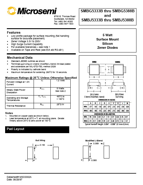
Features
• Low profile package for surface mounting (flat handling surface for accurate placement)
• Zener Voltage 3.3V to 200V • High Surge Current Capability • For available tolerances – see note 1 • Available on Tape and Reel (see EIA std RS-481)
400
14.4
0.39
400
13.4
0.25
300
12.7
0.19
200
12.4
0.10
200
11.5
0.15
200
10.7
0.15
200
10
0.20
200
9.5
0.20
150
9.2
0.22
125
8.6
0.22
125
8.0
0.25
125
7.5
0.257
0.25
75
6.3
0.25
1.1
3.00
1660
1.1
3.00
1750
1.0
3.00
1750
1.0
4.00
1850
0.9
5.00
1850
0.9
5.00
元器件交易网
SMB(G or J)5333B thru SMB(G or J)5333B
Note 1
Devices listed have a ± 5% tolerance on nominal V Z. The suffix A denotes a ± 20% tolerance, suffix C denotes ± 2%, and suffix D denotes ± 1%.
3Bxxxxx-xxx-10CB中文资料
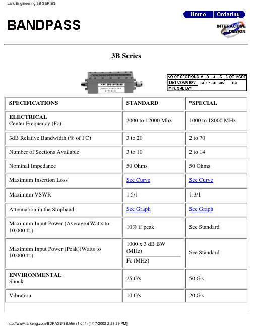
3B SeriesSPECIFICATIONS STANDARD *SPECIAL ELECTRICALCenter Frequency (Fc)2000 to 12000 Mhz 1000 to 18000 MHz 3dB Relative Bandwidth (% of FC) 3 to 20 2 to 70Number of Sections Available 3 to 10 2 to 14Nominal Impedance 50 Ohms 50 Ohms Maximum Insertion Loss See Curve See Curve Maximum VSWR 1.5/1 1.3/1Attenuation in the StopbandSee Graph See Graph Maximum Input Power (Average)(Watts to 10,000 ft.)10% if peak See StandardMaximum Input Power (Peak)(Watts to 10,000 ft.)1000 x 3 dB BW (MHz)Fc (MHz)See StandardENVIRONMENTAL Shock 25 G's 50 G's Vibration10 G's20 G'sHumidity90% relative100% relative Altitude Unlimited UnlimitedTemperature Range (Operating)-25 to + 50 degreescelsius-54 to + 100 degreescelsiusTemperature Range (Non-Operating)-54 to + 70 degreescelsius-62 to +150 degreescelsiusMECHANICALApproximate Weight in oz.0.8 x H x L0.7 x H x LMounting Provisions See below See belowSpecial Configurations Consult Factory Consult FactoryINSERTION LOSS:The Maximum Insertion Loss atcenter frequency is equal to :LF x (N + 0.5) / % 3 dB BW + 0.1Where:LF= Loss Factor, N= Number ofSections% 3dB BW:3dB BW (MHz) x 100divided byCenter Frequency (MHz)Example:A 5 section 3B with a centerfrequency of 10000 MHz and a 3dBBW of 500 MHz would have,.9 x 5.5 / 5 = 0.990.99 + 0.1 = 1.1 dBMECHANICAL SPECIFICATIONSL Dimension = N x (0.3 + 0.5 / %BW)+ 1.0 inch Approx H Dimension = 1450 / Fc(MHz) + 0.6 inch Approx.Connectors Available on 3B SeriesLark Code Type C DIM.Inches & MMLarkCodeType C DIM.Inches & MMA SMA JACK.375 & 9.5*G N JACK.736 & 18.7B SMA PLUG.507 & 12.9*H N PLUG.819 & 20.8*C TNC JACK.750 & 19.1S SPECIAL*D TNC PLUG.844 & 21.4* Not recommended for use with this SeriesThe size shown is a standard used by Lark to facilitate a low cost, easily reproducible unit. Should you require another size, please submit all of your requirements-both electrical and mechanical. This will enable Lark Engineering to quote theoptimum design for your application.STOPBAND SPECIFICATIONSThe graphs on the following pages define the normal specification limits on attenuation Lark bandpass filter series 2B, 3B, and 4B. The minimum level of attenuation in dB is shown as a "number of 3dB bandwidths from centerfrequency".Since the frequency characteristics vary for differing bandwidths, it is necessary to establish specifications for each bandwidth of filter. The different graphs represent various 3dB percentage bandwidths. Intermediate values should be interpolated. The 3dB percentage bandwidth is defined as follows:3dB Bandwidth (MHz) x 100divided byCenter Frequency (MHz)The exact relationship is as follows:1. 3dB Bandwidths From Center Frequency= Rejection Frequency (Mhz) -Center Frequency (Mhz) divided by 3dB Bandwidth (Mhz)Example:Given:2. Center Frequency = 5000 MHz Minimum 3dB Bandwidth = 500 MHzNumber of Sections = 5Find: Minimum attenuation levels at 4250 MHz and 5800 MHz.3dB BW's from Fc = 4250 - 5000 / 500 = - 1.5and 5800 - 5000 / 500 = + 1.6The answer can be read directly from the 10% graph. Using the 5 section curve at the point -1.5 (4250 MHz) we find the minimum level of attenuation is 40dB.At +1.6 (5800 MHz) the minimum level of attenuation is 50dB.For special requirements, please contact our Application EngineeringDepartment.STOPSP3.HTM元器件交易网STOPBAND SPECIFICATIONSSTOPBAND SPECIFICATIONSSTOPSP3.HTM元器件交易网STOPBAND SPECIFICATIONS。
add533 手册
add533 手册【实用版】目录1.引言2.add533 手册的内容概述3.手册的主要章节和重点内容4.如何使用和理解手册5.结论正文1.引言add533 手册是一本非常实用的指南,它涵盖了许多关于 add533 设备的信息和操作方法。
无论是对于初学者还是有经验的用户,这本手册都是非常有价值的参考资料。
在这篇文章中,我们将详细介绍这本手册的内容和如何有效地使用它。
2.add533 手册的内容概述add533 手册主要包括以下几个方面的内容:设备概述、设备安装和配置、操作方法和技巧、故障排除和维护、以及安全注意事项等。
这本手册的目标是帮助用户更好地理解 add533 设备的工作原理,并提供操作指导,以便用户能够更加高效地使用这个设备。
3.手册的主要章节和重点内容在 add533 手册中,以下几个章节是重点内容:- 设备概述:这个章节介绍了 add533 设备的基本信息,包括设备的主要功能、适用场景和使用限制等。
- 设备安装和配置:这个章节提供了详细的安装和配置步骤,包括设备的硬件安装和软件配置等。
- 操作方法和技巧:这个章节主要介绍了如何有效地使用 add533 设备,包括基本操作和进阶技巧等。
- 故障排除和维护:这个章节提供了一些常见的故障排除方法和设备的维护建议,以保证设备的长期稳定运行。
- 安全注意事项:这个章节强调了使用 add533 设备时需要注意的安全问题,以避免可能的安全风险。
4.如何使用和理解手册在使用 add533 手册时,以下几个建议可以帮助你更好地理解和使用手册:- 首先,仔细阅读手册的目录,了解手册的主要内容和结构,以便快速找到你需要的信息。
- 其次,阅读设备概述章节,以便对 add533 设备有一个基本的了解。
- 然后,根据你的需要,选择性地阅读其他章节,以获取更多的操作技巧和故障排除方法。
- 最后,将手册作为参考资料,随时查阅,以便在操作过程中解决可能出现的问题。
5.结论总的来说,add533 手册是一本非常实用的参考资料,它提供了关于add533 设备的全面信息和操作指导。
5833中文资料

5833中⽂资料Designed to reduce logic supply current, chip size, and system cost, the UCN5833A/EP integrated circuits offer high-speed operation for thermal printers. These devices can also be used to drive multi-plexed LED displays or incandescent lamps within their 125 mA peak output current rating. The combination of bipolar and MOS technolo-gies gives BiMOS II smart power ICs an interface flexibility beyond the reach of standard buffers and power driver circuits.These 32-bit drivers have bipolar open-collector npn Darlington outputs, a CMOS data latch for each of the drivers, a 32-bit CMOS shift register, and CMOS control circuitry. The high-speed CMOS shift registers and latches allow operation with most microprocessor-based systems at data input rates above 3.3 MHz. Use of these drivers with TTL may require input pull-up resistors to ensure an input logic high.The UCN5833A is supplied in a 40-pin dual in-line plastic package with 0.600" (15.24 mm) row spacing. At an ambient temperature of +75°C, all outputs of the DlP-packaged device will sustain 50 mA continuously. For high-density applications, the UCN5833EP is available. This 44-lead plastic chip carrier (quad pack) is intended for surface-mounting on solder lands with 0.050" (1.27 mm) centers.CMOS serial data outputs permit cascading for applications requiring additional drive lines.FEATURESI To 3.3 MHz Data Input Rate I 30 V Minimum Output Breakdown I Darlington Current-Sink Outputs I Low-Power CMOS Logic and LatchesBiMOS II 32-BIT SERIAL-INPUT,LATCHED DRIVERAlways order by complete part number:Part Number Package UCN5833A 40-Pin DIP UCN5833EP 44-Lead PLCCData Sheet 26185.16A*58335833BiMOS II 32-BIT SERIAL-INPUT,LATCHED DRIVER115 Northeast Cutoff, Box 15036Worcester, Massachusetts 01615-0036 (508) 853-5000SERIAL DATA IN POWER STROBE OUT OUT OUT OUT OUT OUT 123456OUT7OUT 8OUT 9OUTOUT OUTOUT OUTLOGIC SUPPLY OUT OUT Dwg. No. A-13,051TYPICAL OUTPUT DRIVERSUBOUT115 Northeast Cutoff, Box 15036Worcester, Massachusetts 01615-0036 (508) 853-5000Copyright ? 1986, 1995, Allegro MicroSystems, Inc.5833BiMOS II 32-BIT SERIAL-INPUT,LATCHED DRIVERTRUTH TABLEL = Low Logic Level H = High Logic Level X = Irrelevant P = Present State R = Previous StateELECTRICAL CHARACTERISTICS at T A = +25°C, V DD = 5 V (unless otherwise noted).Limits CharacteristicSymbol Test Conditions Min.Max.Units Output Leakage Current I CEX V OUT = 30 V, T A = 70°C —10µA Collector-Emitter V CE(SAT)l OUT = 50 mA — 1.2V l OUT = 100 mA— 1.7V Input VoltageV IN(1) 3.5 5.3V V IN(0)-0.3+0.8V Input Currentl IN(1)V IN = 5.0 V — 1.0µA l IN(0)V IN = 0 V —-1.0µA Serial Output VoltageV OUT(1)I OUT = -200 µA 4.5—V V OUT(0)I OUT = 200 µA—0.3V Supply Currentl DD One output ON, l OUT = 100 mA — 1.0mA All outputs OFF—50µA Output Rise Time t r l OUT = 100 mA, 10% to 90%—500ns Output Fall Timet fl OUT = 100 mA, 90% to 10%—500nsNOTE: Positive (negative) current is defined as going into (coming out of) the specified device pin.Saturation Voltage5833BiMOS II 32-BIT SERIAL-INPUT,LATCHED DRIVER115 Northeast Cutoff, Box 15036Worcester, Massachusetts 01615-0036 (508) 853-5000TIMING CONDITIONS(V DD = 5.0 V, Logic Levels are V DD and Ground)A.Minimum Data Active Time Before Clock Pulse(Data Set-Up Time)..........................................................................75 ns B.Minimum Data Active Time After Clock Pulse(Data Hold Time).............................................................................75 ns C.Minimum Data Pulse Width ................................................................150 ns D.Minimum Clock Pulse Width...............................................................150 nsE.Minimum Time Between Clock Activation and Strobe.......................300 nsF.Minimum Strobe Pulse Width .............................................................100 nsG.Typical Time Between Strobe Activation andOutput Transition ...........................................................................500 nsDwg. No. A-12,276ASerial Data present at the input is transferred to the shift register on the logic “0” to logic “1” transition of the CLOCK input pulse. On succeeding CLOCK pulses, the registers shift data information towards the SERIAL DATA OUTPUT. The SERIAL DATA must appear at the input prior to the rising edge of the CLOCK input waveform.Information present at any register is transferred to its respective latch when the STROBE is high (serial-to-parallel conversion). The latches will continue to accept new data as long as the STROBE is held high. Applications where the latches are bypassed (STROBE tied high) will require that the OUTPUT ENABLE input be low during serial data entry.When the OUTPUT ENABLE input is low, all of the output buffers are disabled (OFF) without affecting the information stored in the latches or shift register. With the OUTPUT ENABLE input high, the outputs are controlled by the state of the latches.CLOCK DATA INSTROBE NOUTPUT ENABLEOUT5833BiMOS II 32-BIT SERIAL-INPUT,LATCHED DRIVERNOTES:1.Exact body and lead configuration at vendor’s option within limits shown.2.Lead spacing tolerance is non-cumulative.3.Lead thickness is measured at seating plane or below.UCN5833ADimensions in Inches (controlling dimensions)Dimensions in Millimeters (for reference only)123Dwg. MA-003-40 mm20421123Dwg. MA-003-40 in2045833BiMOS II 32-BIT SERIAL-INPUT,LATCHED DRIVER115 Northeast Cutoff, Box 15036Worcester, Massachusetts 01615-0036 (508) 853-5000UCN5833EPDimensions in Inches (controlling dimensions)Dimensions in Millimeters (for reference only)Dwg. MA-005-44A mm0.53340Dwg. MA-005-44A in0.021740NOTES:1.Exact body and lead configuration at vendor’s option within limits shown.2.Lead spacing tolerance is non-cumulative.5833BiMOS II 32-BITSERIAL-INPUT,LATCHED DRIVERThe products described here are manufactured under one or more U.S. patents or U.S. patents pending.Allegro MicroSystems, Inc. reserves the right to make, from time to time, such departures from the detail specifications as may be required to permit improvements in the performance, reliability, or manufacturability of its products. Before placing an order, the user is cautioned to verify that the information being relied upon is current.Allegro products are not authorized for use as critical components in life-support devices or systems without express written approval.The information included herein is believed to be accurate and reliable. However, Allegro MicroSystems, Inc. assumes no responsi-bility for its use; nor for any infringement of patents or other rights of third parties which may result from its use. 5833BiMOS II 32-BIT SERIAL-INPUT,LATCHED DRIVER115 Northeast Cutoff, Box 15036Worcester, Massachusetts 01615-0036 (508) 853-5000POWERINTERFACE DRIVERSFunctionOutput Ratings*Part Number ?SERIAL-INPUT LATCHED DRIVERS8-Bit (saturated drivers)-120 mA 50 V?58958-Bit 350 mA 50 V 58218-Bit 350 mA 80 V 58228-Bit 350 mA 50 V?58418-Bit 350 mA 80 V?58428-Bit (constant-current LED driver)75 mA 17 V 62758-Bit (DMOS drivers)250 mA 50 V 65958-Bit (DMOS drivers)350 mA 50 V?6A5958-Bit (DMOS drivers)100 mA 50 V 6B59510-Bit (active pull-downs)-25 mA 60 V 5810-F and 6809/1012-Bit (active pull-downs)-25 mA 60 V 5811 and 681116-Bit (constant-current LED driver)75 mA 17 V 627620-Bit (active pull-downs)-25 mA 60 V 5812-F and 681232-Bit (active pull-downs)-25 mA 60 V 5818-F and 681832-Bit100 mA 30 V 583332-Bit (saturated drivers)100 mA 40 V 5832PARALLEL-INPUT LATCHED DRIVERS4-Bit350 mA 50 V?58008-Bit -25 mA 60 V 58158-Bit350 mA 50 V?58018-Bit (DMOS drivers)100 mA 50 V 6B2738-Bit (DMOS drivers)250 mA 50 V 6273SPECIAL-PURPOSE DEVICESUnipolar Stepper Motor Translator/Driver 1.25 A 50 V?5804Addressable 8-Bit Decoder/DMOS Driver 250 mA 50 V6259Addressable 8-Bit Decoder/DMOS Driver 350 mA 50 V?6A259Addressable 8-Bit Decoder/DMOS Driver 100 mA 50 V 6B259Addressable 28-Line Decoder/Driver 450 mA30 V6817*Current is maximum specified test condition, voltage is maximum rating. See specification for sustaining voltagelimits.Negative current is defined as coming out of (sourcing) the output.Complete part number includes additional characters to indicate operating temperature range and package style. Internal transient-suppression diodes included for inductive-load protection.。
P6SMB39CAT3G资料

P6SMB11CAT3 Series600 Watt Peak Power Zener Transient Voltage Suppressors Bidirectional*The SMB series is designed to protect voltage sensitive components from high voltage, high energy transients. They have excellent clamping capability, high surge capability, low zener impedance and fast response time. The SMB series is supplied in ON Semiconductor’s exclusive, cost-effective, highly reliable Surmetic t package and is ideally suited for use in communication systems, automotive, numerical controls, process controls, medical equipment, business machines, power supplies and many other industrial/consumer applications.Features•Working Peak Reverse V oltage Range − 9.4 to 77.8 V •Standard Zener Breakdown V oltage Range − 11 to 91 V •Peak Power − 600 W @ 1 ms•ESD Rating of Class 3 (>16 KV) per Human Body Model •Maximum Clamp V oltage @ Peak Pulse Current•Low Leakage < 5 m A Above 10 V•UL 497B for Isolated Loop Circuit Protection •Response Time is Typically < 1 ns•Pb−Free Packages are AvailableMechanical Characteristics:CASE:V oid-Free, Transfer-Molded, Thermosetting Plastic FINISH:All External Surfaces are Corrosion Resistant and Leads are Readily SolderableMAXIMUM CASE TEMPERATURE FOR SOLDERING PURPOSES: 260°C for 10 SecondsLEADS:Modified L−Bend Providing More Contact Area to Bond Pads POLARITY:Polarity Band Will Not be IndicatedMOUNTING POSITION:AnyMAXIMUM RATINGSRating Symbol Value Unit Peak Power Dissipation (Note 1) @ T L = 25°C,Pulse Width = 1 msP PK600WDC Power Dissipation @ T L = 75°C Measured Zero Lead Length (Note 2) Derate Above 75°CThermal Resistance, Junction−to−LeadP DR q JL3.04025WmW/°C°C/WDC Power Dissipation (Note 3) @ T A = 25°C Derate Above 25°CThermal Resistance, Junction−to−AmbientP DR q JA0.554.4226WmW/°C°C/WOperating and Storage Temperature Range T J, Tstg−65 to+150°CStresses exceeding Maximum Ratings may damage the device. Maximum Ratings are stress ratings only. Functional operation above the Recommended Operating Conditions is not implied. Extended exposure to stresses above the Recommended Operating Conditions may affect device reliability.1.10 X 1000 m s, non−repetitive2.1″ square copper pad, FR−4 board3.FR−4 board, using ON Semiconductor minimum recommended footprint, asshown in 403A case outline dimensions spec.*Please see P6SMB6.8AT3 to P6SMB200AT3 for Unidirectional devices.Devices listed in bold, italic are ON Semiconductor Preferred devices. Preferred devices are recommended choices for future use and best overall value.Device Package Shipping†ORDERING INFORMATIONP6SMBxxCAT3SMB2500/T ape & ReelP6SMBxxCAT3G SMB(Pb−Free)2500/T ape & Reel†For information on tape and reel specifications, including part orientation and tape sizes, please refer to our T ape and Reel Packaging Specifications Brochure, BRD8011/D.The “T3” suffix refers to a 13 inch reel.ELECTRICAL CHARACTERISTICS(T A = 25°C unless otherwise noted)Symbol ParameterI PP Maximum Reverse Peak Pulse CurrentV C Clamping Voltage @ I PPV RWM Working Peak Reverse VoltageI R Maximum Reverse Leakage Current @ V RWMV BR Breakdown Voltage @ I TI T Test CurrentQ V BR Maximum Temperature Coefficient of V BRELECTRICAL CHARACTERISTICS (Devices listed in bold, italic are ON Semiconductor Preferred devices.)Device*DeviceMarkingV RWM(Note 4)I R@V RWMBreakdown Voltage V C @ I PP(Note 6)Q V BRC typ(Note 7)V BR Volts (Note 5)@ I T V C I PPVolts m A Min Nom Max mA Volts Amps%/°C pFP6SMB11CAT3, G P6SMB12CAT3, G P6SMB13CAT3, G 11C12C13C9.410.211.155510.511.412.411.051213.0511.612.613.711115.616.718.23836330.0750.0780.081865800740P6SMB15CAT3, G P6SMB16CAT3, G P6SMB18CAT3, G P6SMB20CAT3, G 15C16C18C20C12.813.615.317.1555514.315.217.11915.0516182015.816.818.921111121.222.525.227.7282724220.0840.0860.0880.09645610545490P6SMB22CAT3, G P6SMB24CAT3, G P6SMB27CAT3, G P6SMB30CAT3, G 22C24C27C30C18.820.523.125.6555520.922.825.728.5222427.053023.125.228.431.5111130.633.237.541.420181614.40.090.0940.0960.097450415370335P6SMB33CAT3, G P6SMB36CAT3, G P6SMB39CAT3, G P6SMB43CAT3, G 33C36C39C43C28.230.833.336.8555531.434.237.140.933.053639.0543.0534.737.84145.2111145.749.953.959.313.21211.210.10.0980.0990.10.101305280260240P6SMB47CAT3, G P6SMB51CAT3, G P6SMB56CAT3, G P6SMB62CAT3, G 47C51C56C62C40.243.647.853555544.748.553.258.947.0551.05566249.453.658.865.1111164.870.177859.38.67.87.10.1010.1020.1030.104220205185170P6SMB68CAT3, G P6SMB75CAT3, G P6SMB82CAT3, G P6SMB91CAT3, G 68C75C82C91C58.164.170.177.8555564.671.377.986.56875.05829171.478.886.195.51111921031131256.55.85.34.80.1040.1050.1050.1061551401301204. A transient suppressor is normally selected according to the working peak reverse voltage (V RWM), which should be equal to or greater thanthe DC or continuous peak operating voltage level.5.V BR measured at pulse test current I T at an ambient temperature of 25°C.6.Surge current waveform per Figure 2 and derate per Figure 3 of the General Data − 600 Watt at the beginning of this group.7.Bias Voltage = 0 V, F = 1 MHz, T J = 25°C*The “G’’ suffix indicates Pb−Free package available. Please refer back to Ordering Information on front page.P , P E A K P O W E R (k W )P 1101000.1t, TIME (ms)Figure 2. Pulse WaveformTYPICAL PROTECTION CIRCUITFigure 3. Pulse Derating CurveP E A K P U L S E D E R A T I N G I N % O F P E A K P O W E R O R C U R R E N T @ T A = 25C°T A , AMBIENT TEMPERATURE (°C)Figure 4. Typical Junction Capacitance vs. BiasVoltageBIAS VOLTAGE (VOLTS)110100C , C A P A C I T A N C E (p F )APPLICATION NOTESRESPONSE TIMEIn most applications, the transient suppressor device is placed in parallel with the equipment or component to be protected. In this situation, there is a time delay associated with the capacitance of the device and an overshoot condition associated with the inductance of the device and the inductance of the connection method. The capacitive effect is of minor importance in the parallel protection scheme because it only produces a time delay in the transition from the operating voltage to the clamp voltage as shown in Figure 4.The inductive effects in the device are due to actual turn-on time (time required for the device to go from zero current to full current) and lead inductance. This inductive effect produces an overshoot in the voltage across the equipment or component being protected as shown in Figure 5. Minimizing this overshoot is very important in the application, since the main purpose for adding a transient suppressor is to clamp voltage spikes. The SMB series have a very good response time, typically < 1 ns and negligible inductance. However, external inductive effects could produce unacceptable overshoot. Proper circuit layout, minimum lead lengths and placing the suppressor device as close as possible to the equipment or components to be protected will minimize this overshoot. Some input impedance represented by Z in is essential to prevent overstress of the protection device. This impedance should be as high as possible, without restricting the circuit operation.DUTY CYCLE DERATINGThe data of Figure 1 applies for non-repetitive conditions and at a lead temperature of 25°C. If the duty cycle increases, the peak power must be reduced as indicated by the curves of Figure 6. A verage power must be derated as the lead or ambient temperature rises above 25°C. The average power derating curve normally given on data sheets may be normalized and used for this purpose.At first glance the derating curves of Figure 6 appear to be in error as the 10 ms pulse has a higher derating factor than the 10 m s pulse. However, when the derating factor for a given pulse of Figure 6 is multiplied by the peak power value of Figure 1 for the same pulse, the results follow the expected trend.VFigure 5. Figure 6.Figure 7. Typical Derating Factor for Duty CycleD E R A T I N GF A C T O R10.70.50.30.050.10.010.020.030.07D, DUTY CYCLE (%)UL RECOGNITIONThe entire series has Underwriters Laboratory Recognition for the classification of protectors (QVGV2)under the UL standard for safety 497B and File #116110.Many competitors only have one or two devices recognized or have recognition in a non-protective category. Some competitors have no recognition at all. With the UL497B recognition, our parts successfully passed several testsincluding Strike V oltage Breakdown test, Endurance Conditioning, Temperature test, Dielectric V oltage-Withstand test, Discharge test and several more.Whereas, some competitors have only passed a flammability test for the package material, we have been recognized for much more to be included in their Protector category.PACKAGE DIMENSIONSSMBDO−214AACASE 403A−03ISSUE F*For additional information on our Pb−Free strategy and solderingdetails, please download the ON Semiconductor Soldering andMounting Techniques Reference Manual, SOLDERRM/D.SURMETIC is a trademark of Semiconductor Components Industries, LLC.ON Semiconductor and are registered trademarks of Semiconductor Components Industries, LLC (SCILLC). SCILLC reserves the right to make changes without further notice to any products herein. SCILLC makes no warranty, representation or guarantee regarding the suitability of its products for any particular purpose, nor does SCILLC assume any liability arising out of the application or use of any product or circuit, and specifically disclaims any and all liability, including without limitation special, consequential or incidental damages.“Typical” parameters which may be provided in SCILLC data sheets and/or specifications can and do vary in different applications and actual performance may vary over time. All operating parameters, including “Typicals” must be validated for each customer application by customer’s technical experts. SCILLC does not convey any license under its patent rights nor the rights of others. SCILLC products are not designed, intended, or authorized for use as components in systems intended for surgical implant into the body, or other applications intended to support or sustain life, or for any other application in which the failure of the SCILLC product could create a situation where personal injury or death may occur. Should Buyer purchase or use SCILLC products for any such unintended or unauthorized application, Buyer shall indemnify and hold SCILLC and its officers, employees, subsidiaries, affiliates, and distributors harmless against all claims, costs, damages, and expenses, and reasonable attorney fees arising out of, directly or indirectly, any claim of personal injury or death associated with such unintended or unauthorized use, even if such claim alleges that SCILLC was negligent regarding the design or manufacture of the part. SCILLC is an Equal Opportunity/Affirmative Action Employer. This literature is subject to all applicable copyright laws and is not for resale in any manner.PUBLICATION ORDERING INFORMATION。
MIC5333中文资料

Features
• 2.3V to 5.5V input voltage range • 300mA output current per LDO • Very low quiescent current: 25µA per LDO • POR output with programmable delay for each LDO • High PSRR – >65dB on each LDO • Stable with 1µF ceramic output capacitors • Tiny 10-pin 2.5mm x 2.5mm Thin MLF® package • Ultra-low dropout voltage – 120mV @ 300mA • Low output voltage noise – 50µVrms • Thermal shutdown protection • Current limit protection
2.5mm x 2.5mm Thin MLF-10 (θJA) ...................75°C/W
8
9 10
Pin Name VIN GND
POR2 POR1 EN2 EN1 CSET1
CSET2
VOUT2 VOUT1
Pin Function
Supply Input.
Ground.
Power-On Reset Output (Regulator 2): Open-drain output. Active low indicates an output under-voltage condition on regulator 2 when the device is enabled.
BD533资料
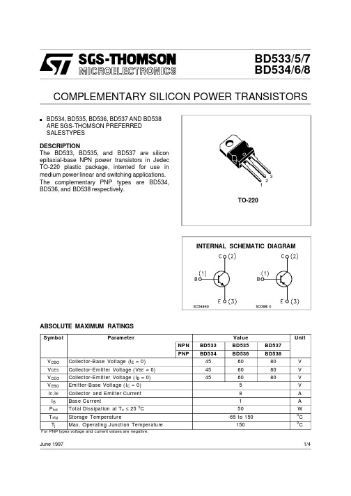
BD533/5/7BD534/6/8COMPLEMENTARY SILICON POWER TRANSISTORSsBD534,BD535,BD536,BD537AND BD538ARE SGS-THOMSON PREFERRED SALESTYPESDESCRIPTIONThe BD533,BD535,and BD537are silicon epitaxial-base NPN power transistors in Jedec TO-220plastic package,intented for use in medium power linear and switching applications.The complementary PNP types are BD534,BD536,and BD538respectively.INTERNAL SCHEMATIC DIAGRAMJune 1997ABSOLUTE MAXIMUM RATINGSSymbolParameterValueUnitNPN BD533BD535BD537PNPBD534BD536BD538V CBO Collector-Base Voltage (I E =0)456080V V CES Collector-Emitter Voltage (V BE =0)456080V V CEO Collector-Emitter Voltage (I B =0)456080V V EBO Emitter-Base Voltage (I C =0)5V I C,I E Collector and Emitter Current 8A I B Base Current1A P t ot Total Dissipation at T c ≤ 25 oC 50WT stg Storage Temperature-65to 150o C T jMax.Operating Junction Temperature150oCFor PNP types voltage and current values are negative.123TO-2201/4THERMAL DATAR t hj-ca se R t hj-amb Thermal Resistance Junction-case MaxThermal Resistance Junction-ambient Max2.570o C/Wo C/WELECTRICAL CHARACTERISTICS(T case=25o C unless otherwise specified)Symbol Parameter Test Conditions Min.Typ.Max.UnitI CBO Collector Cut-offCurrent(I E=0)for BD533/534V CB=45Vfor BD535/536V CB=60Vfor BD537/538V CB=80V100100100µAµAµAI CES Collector Cut-offCurrent(V BE=0)for BD533/534V CE=45Vfor BD535/536V CE=60Vfor BD537/538V CE=80V100100100µAµAµAI EBO Emitter Cut-off Current(I C=0)V EB=5V1mAV CEO(sus)∗Collector-EmitterSustaining Voltage(I B=0)I C=100mA for BD533/534for BD535/536for BD537/538456080VVVV CE(sat)∗Collector-EmitterSaturation Voltage I C=2A I B=0.2AI C=6A I B=0.6A0.80.8VVV BE∗Base-Emitter Voltage I C=2A V CE=2V 1.5V h FE∗DC Current Gain I C=10mA V CE=5Vfor BD533/534for BD535/536for BD537/538 I C=500mA V CE=2VI C=2A V CE=2Vfor BD533/534for BD535/536for BD537/53820 20 15 40 25 25 15f T Transition frequency I C=500mA V CE=1V312MHz ∗ Pulsed:Pulse duration=300µs,duty cycle1.5%For PNP types voltage and current values are negative.Safe Operating AreasBD533/BD534/BD535/BD536/BD537/BD5382/4DIM.mminch MIN.TYP.MAX.MIN.TYP.MAX.A 4.40 4.600.1730.181C 1.23 1.320.0480.051D 2.402.720.0940.107D1 1.270.050E 0.490.700.0190.027F 0.610.880.0240.034F1 1.14 1.700.0440.067F2 1.14 1.700.0440.067G 4.95 5.150.1940.203G1 2.4 2.70.0940.106H210.010.400.3930.409L216.40.645L413.014.00.5110.551L5 2.65 2.950.1040.116L615.2515.750.6000.620L7 6.2 6.60.2440.260L9 3.5 3.930.1370.154DIA.3.75 3.850.1470.151P011CTO-220MECHANICAL DATABD533/BD534/BD535/BD536/BD537/BD5383/4BD533/BD534/BD535/BD536/BD537/BD538Information furnished is believed to be accurate and reliable.However,SGS-THOMSON Microelectronics assumes no responsability for the consequences of use of such information nor for any infringementof patents or other rights of third parties which may results from its use.No license is granted by implication or otherwise under any patent or patent rights of SGS-THOMSON Microelectronics.Specifications mentioned in this publication are subject to change without notice.This publicationsupersedes and replaces all information previously supplied.SGS-THOMSON Microelectronics products are notauthorized for use as critical components in life support devices or systems without express written approval of SGS-THOMSON Microelectonics.©1997SGS-THOMSON Microelectronics-Printed in Italy-All Rights ReservedSGS-THOMSON Microelectronics GROUP OF COMPANIESAustralia-Brazil-Canada-China-France-Germany-Hong Kong-Italy-Japan-Korea-Malaysia-Malta-Morocco-The Netherlands-Singapore-Spain-Sweden-Switzerland-Taiwan-Thailand-United Kingdom-U.S.A...4/4。
- 1、下载文档前请自行甄别文档内容的完整性,平台不提供额外的编辑、内容补充、找答案等附加服务。
- 2、"仅部分预览"的文档,不可在线预览部分如存在完整性等问题,可反馈申请退款(可完整预览的文档不适用该条件!)。
- 3、如文档侵犯您的权益,请联系客服反馈,我们会尽快为您处理(人工客服工作时间:9:00-18:30)。
Features• Low profile package for surface mounting (flat handlingsurface for accurate placement)• Zener Voltage 3.3V to 200V • High Surge Current Capability• For available tolerances – see note 1• Available on Tape and Reel (see EIA std RS-481)Mechanical Data• Standard JEDEC outlines as shown• Terminals gull-wing or c-bend (modified J-bend) tin-lead platedand solderable per MIL-STD-750, method 2026• Polarity is indicated by cathode band• Maximum temperature for soldering: 260oC for 10 seconds.Maximum Ratings @ 25o C Unless Otherwise SpecifiedForward Voltage at 1.0A CurrentV F1.2 VoltsSteady State Power DissipationP (AV)5 Watts See note 2Operating and Storage Temperatures T J , T STG -55o C to+ 150oC Thermal ResistanceR θJL25o C/WNotes1. Mounted on copper pads as shown below.2. Lead temperature at 25o C = T L at mounting plane. Deratelinearly above 25o C to zero power at 150 oC0.070”0.090"0.085”Modified J BendPAD LAYOUTomp onents 21201 Itasca Street Chatsworth! "# $ % ! "#Features• Low profile package for surface mounting (flat handlingsurface for accurate placement)• Zener Voltage 3.3V to 200V • High Surge Current Capability• For available tolerances – see note 1• Available on Tape and Reel (see EIA std RS-481)Mechanical Data• Standard JEDEC outlines as shown• Terminals gull-wing or c-bend (modified J-bend) tin-lead platedand solderable per MIL-STD-750, method 2026• Polarity is indicated by cathode band• Maximum temperature for soldering: 260oC for 10 seconds.Maximum Ratings @ 25o C Unless Otherwise SpecifiedForward Voltage at 1.0A CurrentV F1.2 VoltsSteady State Power DissipationP (AV)5 Watts See note 2Operating and Storage Temperatures T J , T STG -55oC to+ 150oC Thermal ResistanceR θJL25o C/WNotes1. Mounted on copper pads as shown below.2. Lead temperature at 25o C = T L at mounting plane. Deratelinearly above 25o C to zero power at 150 oC! "# $ % ! "#0.070”0.190"0.125”Gull WingPAD LAYOUTMicrosemiPart Number RegulatorVoltage(V Z)TestCurrent(I ZT)MaximumDynamicImpedance(Z Z)(A&B Suffix)MaximumReverseCurrent(I R)@ V RI R TestVoltage(V R)(Non-Suffix& A Suffix)I R TestVoltage(V R)(B,C,DSuffix)MaximumRegulatorCurrent(I ZM)(B,C,D Suffix)MaximumDynamicKneeImpedanceZ zk @ 1.0 mA(A,B,C,D Suffix)MaximumSurgeCurrent(I ZSM)MaximumVoltageRegulation(∆V Z)(A,B,C,DSuffix)Gull-WingLeadC-Bend(Mod – J)V mAdc OHMSµA V V mA OHMS AMPS VOLTSSMBG5333B SMBG5334B SMBG5335B SMBG5336B SMBG5337B SMBJ5333BSMBJ5334BSMBJ5335BSMBJ5336BSMBJ5337B3.33.63.94.34.73803503202902603.02.52.02.02.030015050105.01.01.01.01.01.01.01.01.01.01.0144013201220110010104005005005004502018.717.616.415.30.850.800.540.490.44SMBG5338B SMBG5339B SMBG5340B SMBG5341B SMBG5342B SMBJ5338BSMBJ5339BSMBJ5340BSMBJ5341BSMBJ5342B5.15.66.06.26.82402202002001751.51.01.01.01.01.01.01.01.0101.02.03.03.04.91.02.03.03.05.293086579076570040040030020020014.413.412.712.411.50.390.250.190.100.15SMBG5343B SMBG5344B SMBG5345B SMBG5346B SMBG5347B SMBJ5343BSMBJ5344BSMBJ5345BSMBJ5346BSMBJ5347B7.58.28.79.1101751501501501251.51.52.02.02.01010107.55.06.46.96.256.67.25.76.26.66.97.663058054552047520020020015012510.7109.59.28.60.150.200.200.220.22SMBG5348B SMBG5349B SMBG5350B SMBG5351B SMBG5352B SMBJ5348BSMBJ5349BSMBJ5350BSMBJ5351BSMBJ5352B1112131415125100100100752.52.52.52.52.55.02.01.01.01.08.08.69.410.110.88.49.19.910.611.543039526534031512512510075758.07.57.06.76.30.250.250.250.250.25SMBG5353B SMBG5354B SMBG5355B SMBG5356B SMBG5357B SMBJ5353BSMBJ5354BSMBJ5355BSMBJ5356BSMBJ5357B161718192075706565652.52.52.53.03.01.00.50.50.50.511.512.21313.714.412.212.313.714.415.229528026425023775757575756.05.85.55.35.10.300.350.400.400.40SMBG5358B SMBG5359B SMBG5360B SMBG5361B SMBG5362B SMBJ5358BSMBJ5359BSMBJ5360BSMBJ5361BSMBJ5362B222425272850505050503.53.54.05.06.00.50.50.50.50.515.817.31819.420.116.718.21920.621.2216198190176170751001101201304.74.44.34.13.90.450.550.550.600.60SMBG5363B SMBG5364B SMBG5365B SMBG5366B SMBG5367B SMBJ5363BSMBJ5364BSMBJ5365BSMBJ5366BSMBJ5367B303336394340403030308.0101114200.50.50.50.50.521.623.825.928.13122.825.127.429.732.71581441321221101401501601701903.73.53.33.12.80.600.630.650.650.70SMBG5368B SMBG5369B SMBG5370B SMBG5371B SMBG5372B SMBJ5368BSMBJ5369BSMBJ5370BSMBJ5371BSMBJ5372B4751566062252520202025273540420.50.50.50.50.533.836.740.34344.635.838.842.545.547.1100938679762102302803504002.72.52.32.22.10.800.901.001.201.35SMBG5373B SMBG5374B SMBG5375B SMBG5376B SMBG5377B SMBJ5373BSMBJ5374BSMBJ5375BSMBJ5376BSMBJ5377B6875828791202015151544456575750.50.50.50.50.54954596365.551.75662.26669.270635854.552.55006207207607602.01.91.81.71.61.501.601.802.002.20SMBG5378B SMBG5379B SMBG5380B SMBG5381B SMBG5382B SMBJ5378BSMBJ5379BSMBJ5380BSMBJ5381BSMBJ5382B100110120130140121210108.0901251701902300.50.50.50.50.57279.286.493.61017683.691.293.810647.54339.536.63480010001150125015001.51.41.31.21.22.302.502.502.502.50SMBG5383B SMBG5384B SMBG5385B SMBG5386B SMBG5387B SMBG5388B SMBJ5383BSMBJ5384BSMBJ5385BSMBJ5386BSMBJ5387BSMBJ5388B1501601701801902008.08.08.05.05.05.03303503804304504800.50.50.50.50.50.510811512213013714411412212913714415231.529.42826.42523.61500166017501750185018501.11.11.01.00.90.93.003.003.004.005.005.00Electrical CharacteristicsNote 1Devices listed have a ± 5% tolerance on nominal V Z.The suffix A denotes a ± 20% tolerance, suffix Cdenotes ± 2%, and suffix D denotes ± 1%.Note 2Nominal Zener Voltage (V Z) is read with the device in standard test clips with 3/8 to ½ inch spacing betweenclip and case of the diode. Before reading, the diode isallowed so stabilize for a period of 40 ± 10 millisecondsat 25°C (+8, -2°C).Note 3The Zener impedance (Z ZT or Z ZK is derived from the 60H Z ac voltage, which results when an ac current havinga rms value equal to 10% of the dc zener current (I ZT orI ZK) is superimposed on I ZT or I ZK respectively. Dynamicimpedance variations with other current values aredescribed in Micronote 202.Note 4The Maximum Reverse (leakage) Current is specified for devices with ± 20% and ± 10% voltage toleranceson nominal V Z in another column.Note 5The Maximum Zener Current (I ZM) shown is for ± 5% tolerance devices. I ZM for ± 10% and ± 20% devicescan be calculated using the formula:I ZM = PV ZMWhere “V ZM” is V Z at the high end of the voltagetolerance specified and “P” is the rated power of thedevice.Note 6The Surge Current (I ZM) is specified as the maximum peak of a nonrecurring sine wave of 8.3 millisecondsduration.Note 7Voltage Regulation (∆V Z) is the difference between the voltage measured at 10% and 50% I ZM).。