MAX6386XS34D7+T中文资料
MAX832中文资料
NUAL KIT MA ATION U EET L H A S V A E T WS DA FOLLO
___________________________Features
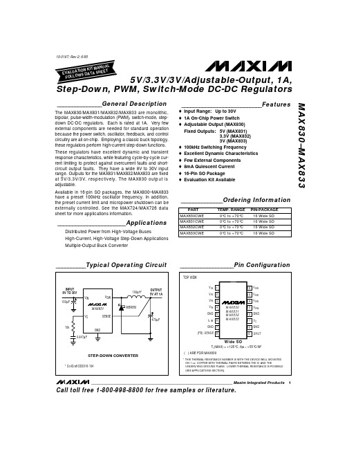
o Input Range: Up to 30V o 1A On-Chip Power Switch o Adjustable Output (MAX830) Fixed Outputs: 5V (MAX831) 3.3V (MAX832) 3V (MAX833) o 100kHz Switching Frequency o Excellent Dynamic Characteristics o Few External Components o 8mA Quiescent Current o 16-Pin SO Package o Evaluation Kit Available
__________Typical Operating Circuit
__________________Pin Configuration
TOP VIEW
INPUT 8V TO 30V 100µF VIN VSW
100µH*
OUTPUT 5V AT 1A
V IN 1 V IN 2 V IN 3
16 V SW 15 V SW 14 V SW
_______________________Applications
Distributed Power from High-Voltage Buses High-Current, High-Voltage Step-Down Applications Multiple-Output Buck Converter
MAX831
VC 10k 0.047µF SENSE
MAX6163AESA-T中文资料

General DescriptionThe MAX6161–MAX6168 are precision, low-dropout,micropower voltage references. These three-terminal devices operate with an input voltage range from (V OUT + 200mV) to 12.6V and are available with output volt-age options of 1.25V, 1.8V, 2.048V, 2.5V, 3V, 4.096V,4.5V, and 5V. They feature a proprietary curvature-cor-rection circuit and laser-trimmed thin-film resistors that result in a very low temperature coefficient of 5ppm/°C (max) and an initial accuracy of ±2mV (max).Specifications apply to the extended temperature range (-40°C to +85°C).The MAX6161–MAX6168 typically draw only 100µA of supply current and can source 5mA (4mA for MAX6161) or sink 2mA of load current. Unlike conven-tional shunt-mode (two-terminal) references that waste supply current and require an external resistor, these devices offer a supply current that is virtually indepen-dent of the supply voltage (8µA/V variation) and do not require an external resistor. Additionally, the internally compensated devices do not require an external com-pensation capacitor. Eliminating the external compen-sation capacitor saves valuable board area in space-critical applications. A low-dropout voltage and a supply-independent, ultra-low supply current make these devices ideal for battery-operated, high-perfor-mance, low-voltage systems.The MAX6161–MAX6168 are available in 8-pin SO packages.________________________ApplicationsAnalog-to-Digital Converters (ADCs)Portable Battery-Powered Systems Notebook Computers PDAs, GPS, DMMs Cellular PhonesPrecision +3V/+5V Systems____________________________Features♦±2mV (max) Initial Accuracy♦5ppm/°C (max) Temperature Coefficient ♦5mA Source Current at 0.9mV/mA ♦2mA Sink Current at 2.5mV/mA ♦Stable with 1µF Capacitive Loads ♦No External Capacitor Required ♦100µA (typ) Quiescent Supply Current ♦200mV (max) Dropout at 1mA Load Current ♦Output Voltage Options: 1.25V, 1.8V, 2.048V, 2.5V,3V, 4.096V, 4.5V, 5V19-1650; Rev 3; 8/05MAX6161–MAX6168Precision, Micropower, Low-Dropout, High-Output-Current, SO-8 Voltage References________________________________________________________________Maxim Integrated Products 1___________________Pin Configuration*Insert the code for the desired initial accuracy and temperature coefficient (from the Selector Guide) in the blank to complete the part number.Typical Operating Circuit and Selector Guide appear at end of data sheet.Ordering InformationFor pricing, delivery, and ordering information,please contact Maxim/Dallas Direct!at 1-888-629-4642, or visit Maxim’s website at .M A X 6161–M A X 6168Precision, Micropower, Low-Dropout, High-Output-Current, SO-8 Voltage References 2_______________________________________________________________________________________ABSOLUTE MAXIMUM RATINGSStresses beyond those listed under “Absolute Maximum Ratings” may cause permanent damage to the device. These are stress ratings only, and functional operation of the device at these or any other conditions beyond those indicated in the operational sections of the specifications is not implied. Exposure to absolute maximum rating conditions for extended periods may affect device reliability.Voltages Referenced to GNDIN …………............................................................-0.3 to +13.5V OUT………………........................................-0.3V to (V IN + 0.3V)Output Short-Circuit Duration to GND or IN (V IN ≤6V)...Continuous Output Short-Circuit Duration to GND or IN (V IN > 6V)…...........60sContinuous Power Dissipation (T A = +70°C)8-Pin SO (derate 5.88mW/°C above +70°C)...............471mW Operating Temperature Range ...........................-40°C to +85°C Storage Temperature Range………….…………-65°C to +150°C Lead Temperature (soldering, 10s)……………………….+300°CELECTRICAL CHARACTERISTICS—MAX6161 (V OUT = 1.25V)MAX6161–MAX6168Precision, Micropower, Low-Dropout, High-Output-Current, SO-8 Voltage References_______________________________________________________________________________________3ELECTRICAL CHARACTERISTICS—MAX6168 (V OUT = 1.800V)M A X 6161–M A X 6168Precision, Micropower, Low-Dropout, High-Output-Current, SO-8 Voltage References 4_______________________________________________________________________________________ELECTRICAL CHARACTERISTICS—MAX6162 (V OUT = 2.048V)MAX6161–MAX6168Precision, Micropower, Low-Dropout, High-Output-Current, SO-8 Voltage References_______________________________________________________________________________________5ELECTRICAL CHARACTERISTICS—MAX6166 (V OUT = 2.500V)M A X 6161–M A X 6168Precision, Micropower, Low-Dropout, High-Output-Current, SO-8 Voltage References 6_______________________________________________________________________________________ELECTRICAL CHARACTERISTICS —MAX6163 (V OUT = 3.000V)MAX6161–MAX6168Precision, Micropower, Low-Dropout, High-Output-Current, SO-8 Voltage References_______________________________________________________________________________________7ELECTRICAL CHARACTERISTICS—MAX6164 (V OUT = 4.096V)M A X 6161–M A X 6168Precision, Micropower, Low-Dropout, High-Output-Current, SO-8 Voltage References 8_______________________________________________________________________________________ELECTRICAL CHARACTERISTICS —MAX6167 (V OUT = 4.500V)MAX6161–MAX6168Precision, Micropower, Low-Dropout, High-Output-Current, SO-8 Voltage References_______________________________________________________________________________________9ELECTRICAL CHARACTERISTICS—MAX6165 (V OUT = 5.000V)Note 2:Temperature Coefficient is specified by the “box” method; i.e., the maximum ΔV OUT is divided by the maximum ΔT.Note 3:Thermal Hysteresis is defined as the change in T A = +25°C output voltage before and after temperature cycling of thedevice (from T A = T MIN to T MAX ). Initial measurement at T A = +25°C is followed by temperature cycling the device to T A = +85°C then to T A = -40°C, and another measurement at T A = +25°C is compared to the original measurement at T A = +25°C.Note 4:Dropout voltage is the minimum input voltage at which V OUT changes ≤0.2% from V OUT at V IN = 5.0V (V IN = 5.5V forMAX6165).M A X 6161–M A X 6168Precision, Micropower, Low-Dropout, High-Output-Current, SO-8 Voltage References 10______________________________________________________________________________________Typical Operating Characteristics(V IN = +5V for MAX6161–MAX6168, V IN = +5.5V for MAX6165, I OUT = 0, T A = +25°C, unless otherwise noted.) (Note 5)MAX6161OUTPUT VOLTAGE TEMPERATURE DRIFTTEMPERATURE (°C)O U T P U T V O L T A G E (V )70552540-1010-251.24961.24971.24981.24991.25001.25011.25021.25031.25041.25051.2495-4085MAX6165OUTPUT VOLTAGE TEMPERATURE DRIFTTEMPERATURE (°C)O U T P U T V O L T A G E (V )7055-25-102510404.99854.99904.99955.00005.00055.00105.00155.00204.9980-4085MAX6161LONG-TERM DRIFTM A X 6161/68 t o c 03TIME (hrs)D R I F T (p p m )768192384576-30-20-100102030405060-40960MAX6165LONG-TERM DRIFTM A X 6161/68 t o c 04TIME (hrs)D R I F T (p p m )768192384576-90-80-70-60-50-40-30-20-100-100960-300-200-100010020030024681012MAX6161LINE REGULATIONINPUT VOLTAGE (V)O U T P U T V O L T A G E C H A N G E (μV )-1200-600-800-1000-400-20002005971113MAX6165LINE REGULATIONINPUT VOLTAGE (V)O U T P U T V O L T A G E C H A N G E (μV )-310-1-22345-4-224LOAD CURRENT (mA)O U T P U T V O L T A G E C H A N G E (m V)MAX6161LOAD REGULATION-620-2-44861012-6-2-4246LOAD CURRENT (mA)O U T P U T V O L T A G E C H A N G E (m V )MAX6165LOAD REGULATION0.100.050.200.150.250.30021345MAX6166DROPOUT VOLTAGE vs. LOAD CURRENTLOAD CURRENT (mA)D R O P O U T V O L T A GE (V )MAX6161–MAX6168Output-Current, SO-8 Voltage References______________________________________________________________________________________11Typical Operating Characteristics (continued)(V IN = +5V for MAX6161–MAX6168, V IN = +5.5V for MAX6165, I OUT = 0, T A = +25°C, unless otherwise noted.) (Note 5)00.050.150.100.200.2521345LOAD CURRENT (mA)D R O P O U T V O L T A GE (V )MAX6165DROPOUT VOLTAGE vs. LOAD CURRENTM A X 6161/68 t o c 11FREQUENCY (kHz)P S R R (d B )0-10-20-30-40-50-60-70-80-900.0011101000.010.11000MAX6161POWER-SUPPLY REJECTION RATIOvs. FREQUENCY-70-800.001101000-60-50-40-30-20-100FREQUENCY (kHz)P S R R (d B )0.1MAX6165POWER-SUPPLY REJECTION RATIOvs. FREQUENCYM A X 6161/68 t c 12MAX6161SUPPLY CURRENT vs. SUPPLY VOLTAGESUPPLY VOLTAGE (V)S U P P L Y C U R R E N T (μA )1210864108116124132140148156164172180100214MAX6165SUPPLY CURRENT vs. SUPPLY VOLTAGESUPPLY VOLTAGE (V)S U P P L Y C U R R E N T (μA )1312101178969610210811412012613213814415090514MAX6161SUPPLY CURRENT vs. TEMPERATURETEMPERATURE (°C)S U P P L Y C U R R E N T (μA )603510-15108116124132140148156164172180100-4085MAX6165SUPPLY CURRENT vs. TEMPERATURETEMPERATURE (°C)S U P P L Y C U R R E N T (μA )603510-159610210811412012613213814415090-408500.00110100040206080100140120160180200220M A X 6161/68 t o c 17FREQUENCY (kHz)O U T P U T I M P E D A N C E (Ω)0.1MAX6161OUTPUT IMPEDANCE vs. FREQUENCY1800.00110100040206010080120140160M A X 6161/68 t o c 18FREQUENCY (kHz)O U T P U T I M P E D A N C E (Ω)0.1MAX6165OUTPUT IMPEDANCE vs. FREQUENCYM A X 6161–M A X 6168Output-Current, SO-8 Voltage References 12______________________________________________________________________________________Typical Operating Characteristics (continued)(V IN = +5V for MAX6161–MAX6168, V IN = +5.5V for MAX6165, I OUT = 0, T A = +25°C, unless otherwise noted.) (Note 5)V OUT 10μV/div 1s/div MAX61610.1Hz TO 10Hz OUTPUT NOISEM A X 6161/68 t o c 19V OUT 10μV/div1s/divMAX6165NOISEM A X 6161/68 t o c 20V OUT 500mV/divV IN 5V/div10μs/divMAX6161TURN-ON TRANSIENT(C L = 50pF)M A X 6161/68 t o c 21V OUT 2V/divV IN 5V/div40μs/divMAX6165TURN-ON TRANSIENT(C L = 50pF)M A X 6161/67 t o c 22I OUT 500μA/divV OUTAC-COUPLED 100mV/div400μs/div MAX6161LOAD TRANSIENT(I OUT = ±250μA, V IN = 5.0, C L = 0)+250μA -250μAMAX6161/68 toc23I OUT 500μA/divV OUTAC-COUPLED50mV/div400μs/divMAX6165LOAD TRANSIENT(I OUT = ±250μA, C L = 0, V IN = 5.5V)+250μA -250μAMAX6161/68 toc24MAX6161–MAX6168Output-Current, SO-8 Voltage References______________________________________________________________________________________13I OUT 5mA/divV OUTAC-COUPLED50mV/div400μs/divMAX6165LOAD TRANSIENT(C L = 0, I OUT = ±2mA, V IN = 5.5V)+2mA -2mAMAX6161/68 toc28I OUT 5mA/divV OUTAC-COUPLED 100mV/div 400μs/div MAX6161LOAD TRANSIENT(V IN = 5.0V, C L = 0, I OUT = ±2mA)+2mA-2mAMAX6161/68 toc27I OUT 5mA/divV OUTAC-COUPLED50mV/div400μs/divMAX6161LOAD TRANSIENT(V IN = 5.0V, C L = 1μF, I OUT = ±2mA)+2mA-2mAMAX6161/68 toc29I OUT 5mA/divV OUTAC-COUPLED20mV/div400μs/divMAX6165LOAD TRANSIENT(C L = 1μF, I OUT = ±2mA, V IN = 5.5V)+2mA-2mAMAX6161/68 toc30I OUT 500μA/divV OUTAC-COUPLED10mV/div 400μs/div MAX6161LOAD TRANSIENT(I OUT = ±250μA, V IN = 5.0V, C L = 1μF)+250μA -250μAMAX6161/68 toc25I OUT 500μA/divV OUTAC-COUPLED20mV/div400μs/divMAX6165LOAD TRANSIENT(I OUT = ±250μA, C L = 1μF, V IN = 5.5V)+250μA-250μAMAX6161/68 toc26Typical Operating Characteristics (continued)(V IN = +5V for MAX6161–MAX6168, V IN = +5.5V for MAX6165, I OUT = 0, T A = +25°C, unless otherwise noted.) (Note 5)M A X 6161–M A X 6168Output-Current, SO-8 Voltage References 14______________________________________________________________________________________I OUT 5mA/divV OUTAC-COUPLED50mV/div 400μs/div MAX6161LOAD TRANSIENT(V IN = 5.0V, C L = 1μF, I OUT = ±4mA)+4mA-4mAMAX6161/68 toc33I OUT 5mA/divV OUTAC-COUPLED50mV/div400μs/divMAX6165LOAD TRANSIENT(I OUT = ±5mA, C L = 1μF, V IN = 5.5V)+5mA-5mAMAX6161/68 toc34V IN500mV/divV OUTAC-COUPLED20mV/div 40μs/div MAX6161LINE TRANSIENT(C L = 0)+0.25V-0.25VMAX6161/68 toc35V IN500mV/divV OUTAC-COUPLED20mV/div40μs/divMAX6165LINE TRANSIENT(C L = 0)+0.25V -0.25VMAX6161/68 toc36Note 5:Many of the Typical Operating Characteristics of the MAX6161 family are extremely similar. The extremes of these characteristicsare found in the MAX6161 (1.25V output) and the MAX6165 (5.0V output). The Typical Operating Characteristics of the remain-der of the MAX6161 family typically lie between these two extremes and can be estimated based on their output voltages.Typical Operating Characteristics (continued)(V IN = +5V for MAX6161–MAX6168, V IN = +5.5V for MAX6165, I OUT = 0, T A = +25°C, unless otherwise noted.) (Note 5)I OUT 5mA/divV OUTAC-COUPLED 200mV/div400μs/div MAX6161LOAD TRANSIENT(V IN = 5.0V, C L = 0, I OUT = ±4mA)+4mA-4mAMAX6161/68 toc31I OUT 5mA/divV OUTAC-COUPLED 100mV/div400μs/divMAX6165LOAD TRANSIENT(I OUT = ±5mA, C L = 0, V IN = 5.5V)+5mA-5mAMAX6161/68 toc32MAX6161–MAX6168Output-Current, SO-8 Voltage References______________________________________________________________________________________15Applications InformationInput BypassingF or the best line-transient performance, decouple the input with a 0.1µF ceramic capacitor as shown in the Typical Operating Circuit . Locate the capacitor as close to IN as possible. When transient performance is less important, no capacitor is necessary.Output/Load CapacitanceDevices in the MAX6161 family do not require an output capacitor for frequency stability. In applications where the load or the supply can experience step changes,an output capacitor of at least 0.1µF will reduce the amount of overshoot (undershoot) and improve the cir-cuit’s transient response. Many applications do not require an external capacitor, and the MAX6161 family can offer a significant advantage in applications when board space is critical.Supply CurrentThe quiescent supply current of the series-mode MAX6161 family is typically 100µA and is virtually inde-pendent of the supply voltage, with only an 8µA/V (max) variation with supply voltage. Unlike series refer-ences, shunt-mode references operate with a series resistor connected to the power supply. The quiescent current of a shunt-mode reference is thus a function of the input voltage. Additionally, shunt-mode references have to be biased at the maximum expected load cur-rent, even if the load current is not present at the time.In the MAX6161 family, the load current is drawn from the input voltage only when required, so supply current is not wasted and efficiency is maximized at all input voltages. This improved efficiency reduces power dissi-pation and extends battery life.When the supply voltage is below the minimum speci-fied input voltage (as during turn-on), the devices can draw up to 400µA beyond the nominal supply current.The input voltage source must be capable of providing this current to ensure reliable turn-on.Output Voltage HysteresisOutput voltage hysteresis is the change in the input voltage at T A = +25°C before and after the device is cycled over its entire operating temperature range.Hysteresis is caused by differential package stress appearing across the bandgap core transistors. The typical temperature hysteresis value is 125ppm.Turn-On TimeThese devices typically turn on and settle to within 0.1% of their final value in 50µs to 300µs, depending on the output voltage (see electrical table of part used).The turn-on time can increase up to 1.5ms with the device operating at the minimum dropout voltage and the maximum load.Typical Operating Circuit__________________________Chip Information TRANSISTOR COUNT: 117PROCESS: BiCMOSPin DescriptionPIN NAME FUNCTIONNo Connection. Not internally connected.N.C.1, 3, 5, 7, 82IN Input Voltage GroundGND 46OUTReference OutputM A X 6161–M A X 6168Output-Current, SO-8 Voltage References 16______________________________________________________________________________________Selector GuideMAX6161–MAX6168Maxim cannot assume responsibility f or use of any circuitry other than circuitry entirely embodied in a Maxim product. No circuit patent licenses are implied. Maxim reserves the right to change the circuitry and specifications without notice at any time.Maxim Integrated Products, 120 San Gabriel Drive, Sunnyvale, CA 94086 408-737-7600_____________________17©2005 Maxim Integrated ProductsPrinted USAis a registered trademark of Maxim Integrated Products, Inc.S O I C N .E P SOutput-Current, SO-8 Voltage ReferencesPackage Information(The package drawing(s) in this data sheet may not reflect the most current specifications. For the latest package outline information go to /packages .)。
MAX6387XS33D7-T中文资料

General DescriptionThe MAX6381–MAX6390 microprocessor (µP) supervisory circuits monitor power supply voltages from +1.8V to +5.0V while consuming only 3µA of supply current at +1.8V. Whenever V CC falls below the factory-set reset thresholds, the reset output asserts and remains assert-ed for a minimum reset timeout period after V CC rises above the reset threshold. Reset thresholds are available from +1.58V to +4.63V, in approximately 100mV incre-ments. Seven minimum reset timeout delays ranging from 1ms to 1200ms are available.The MAX6381/MAX6384/MAX6387 have a push-pull active-low reset output. The MAX6382/MAX6385/MAX6388 have a push-pull active-high reset output,and the MAX6383/MAX6386/MAX6389/MAX6390 have an open-drain active-low reset output. The MAX6384/MAX6385/MAX6386 also feature a debounced manual reset input (with internal pullup resistor). The MAX6387/MAX6388/MAX6389 have an auxiliary input for monitoring a second voltage. The MAX6390 offers a manual reset input with a longer V CC reset timeout period (1120ms or 1200ms) and a shorter manual reset timeout (140ms or 150ms).The MAX6381/MAX6382/MAX6383 are available in 3-pin SC70 packages and the MAX6384–MAX6390 are avail-able in 4-pin SC70 packages.________________________ApplicationsComputers ControllersIntelligent InstrumentsCritical µP and µC Power Monitoring Portable/Battery-Powered Equipment Dual Voltage SystemsFeatureso Factory-Set Reset Threshold Voltages Ranging from +1.58V to +4.63V in Approximately 100mV Increments o ±2.5% Reset Threshold Accuracy Over Temperature (-40°C to +125°C)o Seven Reset Timeout Periods Available: 1ms,20ms, 140ms, 280ms, 560ms, 1120ms, 1200ms (min)o 3 Reset Output OptionsActive-Low Push-Pull Active-High Push-Pull Active-Low Open-Draino Reset Output State Guaranteed Valid Down to V CC = 1Vo Manual Reset Input (MAX6384/MAX6385/MAX6386)o Auxiliary RESET IN(MAX6387/MAX6388/MAX6389)o V CC Reset Timeout (1120ms or 1200ms)/Manual Reset Timeout (140ms or 150ms) (MAX6390)o Negative-Going V CC Transient Immunity o Low Power Consumption of 6µA at +3.6V and 3µA at +1.8V o Pin Compatible withMAX809/MAX810/MAX803/MAX6326/MAX6327/MAX6328/MAX6346/MAX6347/MAX6348, and MAX6711/MAX6712/MAX6713o Tiny 3-Pin SC70 and 4-Pin SC70 PackagesMAX6381–MAX6390SC70, Single/Dual Low-Voltage, Low-Power µP Reset Circuits________________________________________________________________Maxim Integrated Products1Pin Configurations19-1839; Rev 1; 04/01Ordering InformationOrdering Information continued at end of data sheet.Typical Operating Circuit appears at end of data sheet.Selector Guide appears at end of data sheet.Note:Insert reset threshold suffix (see Reset Threshold table)after "XR" or "XS". Insert reset timeout delay (see Reset Timeout Delay table) after "D" to complete the part number. Sample stock is generally held on standard versions only (seeStandard Versions table). Standard versions have an order increment requirement of 2500 pieces. Nonstandard versions have an order increment requirement of 10,000 pieces.Contact factory for availability of nonstandard versions.*MAX6390 is available with D4 or D7 timing only.For pricing, delivery, and ordering information,please contact Maxim/Dallas Direct!at 1-888-629-4642, or visit Maxim’s website at .M A X 6381–M A X 6390SC70, Single/Dual Low-Voltage, Low-Power µP Reset CircuitsABSOLUTE MAXIMUM RATINGSELECTRICAL CHARACTERISTICSStresses beyond those listed under “Absolute Maximum Ratings” may cause permanent damage to the device. These are stress ratings only, and functional operation of the device at these or any other conditions beyond those indicated in the operational sections of the specifications is not implied. Exposure to absolute maximum rating conditions for extended periods may affect device reliability.V CC to GND..........................................................-0.3V to +6.0V RESET Open-Drain Output....................................-0.3V to +6.0V RESET , RESET (Push-Pull Output).............-0.3V to (V CC + 0.3V)MR , RESET IN.............................................-0.3V to (V CC + 0.3V)Input Current (V CC ).............................................................20mA Output Current (All Pins).....................................................20mAContinuous Power Dissipation (T A = +70°C)3-Pin SC70 (derate 2.9mW/°C above +70°C)........235mW 4-Pin SC70 (derate 3.1mW/°C above +70°C)........245mW Operating Temperature Range .........................-40°C to +125°C Storage Temperature Range.............................-65°C to +150°C Lead Temperature (soldering, 10s).................................+300°CMAX6381–MAX6390SC70, Single/Dual Low-Voltage, Low-Power µP Reset Circuits_______________________________________________________________________________________3M A X 6381–M A X 6390SC70, Single/Dual Low-Voltage, Low-Power µP Reset Circuits 4______________________________________________________________________________________Typical Operating Characteristics(T A = +25°C, unless otherwise noted.)215436789-40-105-25203550658095110125SUPPLY CURRENT vs. TEMPERATURE(NO LOAD)TEMPERATURE (°C)S U P P L Y C U R R E N T (µA )25292735333137394143-40-105-25203550658095110125POWER-DOWN RESET DELAYvs. TEMPERATURETEMPERATURE (°C)P O W E R -D O W N R E S E T D E L A Y (µs )0.940.980.961.021.001.061.041.08-40-10520-253550658095110125NORMALIZED POWER-UP RESET TIMEOUTvs. TEMPERATUREM A X 6381/90 t o c 03TEMPERATURE (°C)N O R M A L I Z E D R E S E T T I M E O U T P E R I O D0.9900.9851.0150.9950.9901.0001.0051.0101.020-40-10520-253550958011065125M A X 6381/90 t o c 04TEMPERATURE (°C)N O R M A L I Z E D R E S E TT H R E S H O L D NORMALIZED RESET THRESHOLDvs. TEMPERATURE00.40.20.80.61.01.2063912OUTPUT VOLTAGE LOW vs. SINK CURRENTI SINK (mA)V O L (V )01.00.52.01.52.53.00500750250100012501500OUTPUT VOLTAGE HIGH vs. SOURCE CURRENTI SOURCE (µA)V O H (V )45001100010010MAXIMUM TRANSIENT DURATION vs. RESET COMPARATOR OVERDRIVE15050350250500200100400300RESET COMPARATOR OVERDRIVE, V TH - V CC (mV)M A X I M U M T R A N S I E N T D U R A T I O N (µs )3.53.93.74.54.34.14.74.95.35.15.5-40-105-25203550658095110125RESET IN TO RESET DELAYvs. TEMPERATUREM A X 6381/90 t o c 08TEMPERATURE (°C)R E S E T I N D E L A Y (µs )MAX6381–MAX6390SC70, Single/Dual Low-Voltage, Low-Power µP Reset Circuits_______________________________________________________________________________________5M A X 6381–M A X 6390SC70, Single/Dual Low-Voltage, Low-Power µP Reset Circuits 6_______________________________________________________________________________________Detailed DescriptionRESET OutputA µP reset input starts the µP in a known state. These µP supervisory circuits assert reset to prevent code execution errors during power-up, power-down, or brownout conditions.Reset asserts when V CC is below the reset threshold;once V CC exceeds the reset threshold, an internal timer keeps the reset output asserted for the reset timeout period. After this interval, reset output deasserts. Reset output is guaranteed to be in the correct logic state for V CC ≥1V.Manual Reset Input (MAX6384/MAX6385/MAX6386/MAX6390)Many µP-based products require manual reset capabil-ity, allowing the operator, a test technician, or external logic circuitry to initiate a reset. A logic low on MR asserts reset. Reset remains asserted while MR is low,and for the reset active timeout period (t RP ) after MR returns high. This input has an internal 63k Ωpullup resistor (1.35k Ωfor MAX6390), so it can be left uncon-nected if it is not used. MR can be driven with TTL or CMOS logic levels, or with open-drain/collector outputs.Connect a normally open momentary switch from MR to G ND to create a manual-reset function; external debounce circuitry is not required. If MR is driven from long cables or if the device is used in a noisy environ-ment, connecting a 0.1µF capacitor from MR to G ND provides additional noise immunity.RESET IN Comparator(MAX6387/MAX6388/MAX6389)RESET IN is compared to an internal +1.27V reference.If the voltage at RESET IN is less than 1.27V, reset asserts. Use the RESET IN comparator as a user-adjustable reset detector or as a secondary power-sup-ply monitor by implementing a resistor-divider at RESET IN (shown in Figure 1). Reset asserts when either V CC or RESET IN falls below its respective threshold volt-age. Use the following equation to set the threshold:V INTH = V THRST (R1/R2 + 1)where V THRST = +1.27V. To simplify the resistor selec-tion, choose a value of R2 and calculate R1:R1 = R2 [(V INTH /V THRST ) - 1]Since the input current at RESET IN is 50nA (max),large values can be used for R2 with no significant loss in accuracy.___________Applications InformationNegative-Going V CC TransientsIn addition to issuing a reset to the µP during power-up,power-down, and brownout conditions, the MAX6381–MAX6390 are relatively immune to short dura-tion negative-going V CC transients (glitches).The Typical Operating Characteristics section shows the Maximum Transient Durations vs. Reset Comparator Overdrive, for which the MAX6381–MAX6390 do not generate a reset pulse. This graph was generated usinga negative-going pulse applied to V CC , starting above the actual reset threshold and ending below it by the magni-tude indicated (reset comparator overdrive). The graph indicates the typical maximum pulse width a negative-going V CC transient may have without causing a reset pulse to be issued. As the magnitude of the transient increases (goes farther below the reset threshold), the maximum allowable pulse width decreases. A 0.1µF capacitor mounted as close as possible to V CC provides additional transient immunity.Ensuring a Valid RESET Output Down to V CC = 0The MAX6381–MAX6390 are guaranteed to operate properly down to V CC = 1V. In applications that require valid reset levels down to V CC = 0, a pulldown resistor to active-low outputs (push/pull only, Figure 2) and a pullup resistor to active-high outputs (push/pull only) will ensure that the reset line is valid while the reset output can no longer sink or source current. This scheme doesnot work with the open-drain outputs of the MAX6383/MAX6386/MAX6389/MAX6390. The resistor value used is not critical, but it must be small enough not to load the reset output when V CC is above the reset threshold. For most applications, 100k Ωis adequate.MAX6381–MAX6390SC70, Single/Dual Low-Voltage, Low-Power µP Reset Circuits_______________________________________________________________________________________7M A X 6381–M A X 6390SC70, Single/Dual Low-Voltage, Low-Power µP Reset Circuits 8Selector GuideChip InformationTRANSISTOR COUNT: 647PROCESS: BiCMOS*MR is for MAX6384/MAX6385/MAX6386/MAX6390**RESET IN is for MAX6387/MAX6388/MAX6389( ) are for MAX6382/MAX6385/MAX6388Pin Configurations (continued)MAX6381–MAX6390SC70, Single/Dual Low-Voltage, Low-Power µP Reset Circuits_______________________________________________________________________________________9Ordering Information(continued)Note:Insert reset threshold suffix (see Reset Threshold table)after "XR" or "XS". Insert reset timeout delay (see Reset Timeout Delay table) after "D" to complete the part number. Sample stock is generally held on standard versions only (seeStandard Versions table). Standard versions have an order increment requirement of 2500 pieces. Nonstandard versions have an order increment requirement of 10,000 pieces.Contact factory for availability of nonstandard versions.*MAX6390 is available with D4 or D7 timing only.M A X 6381–M A X 6390SC70, Single/Dual Low-Voltage, Low-Power µP Reset Circuits 10______________________________________________________________________________________Package InformationSC70, Single/Dual Low-Voltage, Low-Power µP Reset CircuitsMaxim cannot assume responsibility for use of any circuitry other than circuitry entirely embodied in a Maxim product. No circuit patent licenses are implied. Maxim reserves the right to change the circuitry and specifications without notice at any time.Maxim Integrated Products, 120 San Gabriel Drive, Sunnyvale, CA 94086 408-737-7600____________________11©2001 Maxim Integrated Products Printed USA is a registered trademark of Maxim Integrated Products.MAX6381–MAX6390Package Information (continued)元器件交易网。
MAX4636中文资料

元器件交易网
Fast, Low-Voltage, Dual 4Ω SPDT CMOS Analog Switches MAX4635/MAX4636
ABSOLUTE MAXIMUM RATINGS
(Voltages Referenced to GND) V+, IN_ .....................................................................-0.3V to +6V COM_, NC_, NO_ (Note 1) .......................... -0.3V to (V+ + 0.3V) Continuous Current into Any Terminal .............................±30mA Peak Current into COM_, NC_, NO_ (pulsed at 1ms, 10% duty cycle).................................±100mA Continuous Power Dissipation (TA = +70°C) 10-Pin µMAX (derate 4.7mW/°C above +70°C) ............330mW 10-Pin Thin QFN (derate 24.4mW/°C above +70°C) ..1951mW Operating Temperature Range .......................... -40°C to +85°C Storage Temperature Range ........................... -65°C to +150°C Lead Temperature (soldering, 10s) ............................... +300°C
MAXIM MAX9376 说明书
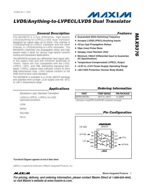
General DescriptionThe MAX9376 is a fully differential, high-speed,LVDS/anything-to-LVPECL/LVDS dual translator designed for signal rates up to 2GH z. One channel is LVDS/anything-to-LVPECL translator and the other channel is LVDS/anything-to-LVDS translator. The MAX9376’s extremely low propagation delay and high speed make it ideal for various high-speed network routing and backplane applications.The MAX9376 accepts any differential input signal with-in the supply rails and with minimum amplitude of 100mV. Inputs are fully compatible with the LVDS,LVPECL, H STL, and CML differential signaling stan-dards. LVPECL outputs have sufficient current to drive 50Ωtransmission lines. LVDS outputs conform to the ANSI EIA/TIA-644 LVDS standard.The MAX9376 is available in a 10-pin µMAX ®package and operates from a single +3.3V supply over the -40°C to +85°C temperature range.ApplicationsBackplane Logic Standard Translation LVDS-to-LVPECL, LVPECL-to-LVDS Up/Downconverters LANs WANs DSLAMs DLCsFeatureso Guaranteed 2GHz Switching Frequency o Accepts LVDS/LVPECL/Anything Inputs o 421ps (typ) Propagation Delays o 30ps (max) Pulse Skew o 2ps RMS (max) Random Jittero Minimum 100mV Differential Input to Guarantee AC Specifications o Temperature-Compensated LVPECL Output o +3.0V to +3.6V Power-Supply Operating Range o >2kV ESD Protection (Human Body Model)MAX9376LVDS/Anything-to-LVPECL/LVDS Dual Translator________________________________________________________________Maxim Integrated Products 1Pin Configuration19-2809; Rev 1; 10/09For pricing, delivery, and ordering information,please contact Maxim Direct at 1-888-629-4642,or visit Maxim’s website at .Functional Diagram appears at end of data sheet.+Denotes a lead(Pb)-free/RoHS-compliant package.µMAX is a registered trademark of Maxim Integrated Products, Inc.M A X 9376LVDS/Anything-to-LVPECL/LVDS Dual TranslatorABSOLUTE MAXIMUM RATINGSDC ELECTRICAL CHARACTERISTICS(V CC = +3.0V to +3.6V, differential input voltage |V ID | = 0.1V to 3.0V, input voltage (V IN , V IN ) = 0 to V CC , input common-mode voltage V CM = 0.05V to (V CC - 0.05V), LVPECL outputs terminated with 50Ω±1% to (V CC - 2.0V), LVDS outputs terminated with 100Ω±1%, Stresses beyond those listed under “Absolute Maximum Ratings” may cause permanent damage to the device. These are stress ratings only, and functional operation of the device at these or any other conditions beyond those indicated in the operational sections of the specifications is not implied. Exposure to absolute maximum rating conditions for extended periods may affect device reliability.V CC to GND...........................................................-0.3V to +4.1V Inputs (IN_, IN_).........................................-0.3V to (V CC + 0.3V)IN to IN ................................................................................±3.0V Continuous Output Current.................................................50mA Surge Output Current .......................................................100mA Continuous Power Dissipation (T A = +70°C)10-Pin µMAX (derate 5.6mW/°C above +70°C)..........444mWθJA in Still Air (Note 1)............................................+180°C/W Junction Temperature......................................................+150°C Storage Temperature Range.............................-65°C to +150°C ESD Protection Human Body Model (IN_, IN_, OUT_, OUT_)..................≥2kV Soldering Temperature (10s)...........................................+300°C Note 1:Package thermal resistances were obtained using the method described in JEDEC specification JESD51-7, using a four-layer board. For detailed information on package thermal considerations, refer to /thermal-tutorial .MAX9376LVDS/Anything-to-LVPECL/LVDS Dual Translator_______________________________________________________________________________________3AC ELECTRICAL CHARACTERISTICS(V CC = +3.0V to +3.6V, differential input voltage |V ID | = 0.1V to 1.2V, input frequency ≤1.34GHz, differential input transition time =125ps (20% to 80%), input voltage (V IN , V IN ) = 0 to V CC , input common-mode voltage (V CM ) = 0.05V to (V CC - 0.05V), LVPECL out-DC ELECTRICAL CHARACTERISTICS (continued)(V CC = +3.0V to +3.6V, differential input voltage |V ID | = 0.1V to 3.0V, input voltage (V IN , V IN ) = 0 to V CC , input common-mode voltage V CM = 0.05V to (V CC - 0.05V), LVPECL outputs terminated with 50Ω±1% to (V CC - 2.0V), LVDS outputs terminated with 100Ω±1%, T A = -40°C to +85°C. Typical values are at V CC = +3.3V, |V ID | = 0.2V, input common-mode voltage V CM = 1.2V, T A = +25°C, unless otherwise noted.) (Notes 2, 3, 4)M A X 9376LVDS/Anything-to-LVPECL/LVDS Dual Translator 4_______________________________________________________________________________________SUPPLY CURRENT vs. FREQUENCYFREQUENCY (MHz)S U P P L Y C U R R E N T (m A )150010005001020304050002000OUTPUT AMPLITUDE vs. FREQUENCYFREQUENCY (MHz)O U T P U T A M P L I T U D E (m V )1500100050040050060070080090030002000PROPAGATION DELAY vs. TEMPERATURETEMPERATURE (°C)P R O P A G A T I O N D E L A Y (p s )603510-15320340360380400420440460480500300-4085OUTPUT RISE/FALL TIME vs. TEMPERATURETEMPERATURE (°C)O U T P U T R I S E /F A L L T I M E (p s )603510-15809010011012013014070-4085Typical Operating Characteristics(V CC = +3.3V, differential input voltage |V ID | = 0.2V, V CM = 1.2V, input frequency = 500MHz, LVPECL outputs terminated with 50Ω±1% to V CC - 2.0V, LVDS outputs terminated with 100Ω±1%, T A = +25°C, unless otherwise noted.)AC ELECTRICAL CHARACTERISTICS (continued)(V CC = +3.0V to +3.6V, differential input voltage |V ID | = 0.1V to 1.2V, input frequency ≤1.34GHz, differential input transition time =125ps (20% to 80%), input voltage (V IN , V IN ) = 0 to V CC , input common-mode voltage (V CM ) = 0.05V to (V CC - 0.05V), LVPECL out-puts terminated with 50Ω±1% to (V CC - 2.0V), LVDS outputs terminated with 100Ω±1%, T A = -40°C to +85°C. Typical values are at V = +3.3V, |V | = 0.2V, input common-mode voltage V = 1.2V, T = +25°C, unless otherwise noted.) (Note 5)V OD , and ΔV OD .Note 3:Current into a pin is defined as positive. Current out of a pin is defined as negative.Note 4:DC parameters production tested at T A = +25°C and guaranteed by design and characterization over the full operatingtemperature range.Note 5:Guaranteed by design and characterization, not production tested. Limits are set at ±6 sigma.Note 6:t SKEW is the magnitude difference of differential propagation delays for the same output under same conditions; t SKEW =|t PHL - t PLH |.Note 7:Device jitter added to the input signal.MAX9376LVDS/Anything-to-LVPECL/LVDS Dual Translator_______________________________________________________________________________________5M A X 9376LVDS/Anything-to-LVPECL/LVDS Dual Translator 6_______________________________________________________________________________________Applications InformationLVPECL Output TerminationTerminate the MAX9376 LVPECL outputs with 50Ωto (V CC - 2V) or use equivalent Thevenin terminations.Terminate OUT1 and OUT1with identical termination on each for low output distortion. When a single-ended signal is taken from the differential output, terminate both OUT1 and OUT1.Ensure that output currents do not exceed the current limits as specified in the Absolute Maximum Ratings .Under all operating conditions, the device’s total ther-mal limits should be observed.LVDS Output TerminationThe MAX9376 LVDS outputs are current-steering devices; no output voltage is generated without a termi-nation resistor. The termination resistors should match the differential impedance of the transmission line.Output voltage levels are dependent upon the value of the termination resistor. The MAX9376 is optimized for point-to-point interface with 100Ωtermination resistors at the receiver inputs. Termination resistance values may range between 90Ωand132Ω, depending on the characteristic impedance of the transmission medium.Supply BypassingBypass V CC to ground with high-frequency surface-mount ceramic 0.1µF and 0.01µF capacitors. Place the capacitors as close to the device as possible with the 0.01µF capacitor closest to the device pins.TracesCircuit board trace layout is very important to maintain the signal integrity of high-speed differential signals.Maintaining integrity is accomplished in part by reduc-ing signal reflections and skew, and increasing com-mon-mode noise immunity.Signal reflections are caused by discontinuities in the 50Ωcharacteristic impedance of the traces. Avoid dis-continuities by maintaining the distance between differ-ential traces, not using sharp corners or using vias.Maintaining distance between the traces also increases common-mode noise immunity. Reducing signal skew is accomplished by matching the electrical length of the differential traces.Figure 1. Input DefinitionFigure 3. Differential Input-to-Output Propagation Delay Timing DiagramMAX9376LVDS/Anything-to-LVPECL/LVDS Dual Translator_______________________________________________________________________________________7Chip InformationPROCESS: BipolarPackage InformationFor the latest package outline information and land patterns, go to /packages . Note that a “+”, “#”, or “-” in the package code indicates RoHS status only. Package draw-ings may show a different suffix character, but the drawing per-tains to the package regardless of RoHS status.M A X 9376LVDS/Anything-to-LVPECL/LVDS Dual Translator Maxim cannot assume responsibility for use of any circuitry other than circuitry entirely embodied in a Maxim product. No circuit patent licenses are implied. Maxim reserves the right to change the circuitry and specifications without notice at any time.8_____________________Maxim Integrated Products, 120 San Gabriel Drive, Sunnyvale, CA 94086 408-737-7600©2009 Maxim Integrated ProductsMaxim is a registered trademark of Maxim Integrated Products, Inc.。
MAX038中文资料

MAX038中⽂资料
MAX038 频率⾼、精度好,因此它被称为⾼频精密函数信号发⽣器IC。
在锁相环、压控振荡器、频率合成器、脉宽调制器等电路的设计上,MAX038 都是优选的器件。
其内部电路框图如图1 所⽰。
MAX038 的性能特点:
1)能精密地产⽣三⾓波、锯齿波、矩形波(含⽅波)、正弦波信号。
2)频率范围从0.1Hz~20MHz,最⾼可达40MHz,各种波形的输出幅度均为2V(P-P)。
3)占空⽐调节范围宽,占空⽐和频率均可单独调节,⼆者互不影响,占空⽐最⼤调节范围是10%~90%。
4)波形失真⼩,正弦波失真度⼩于0.75%,占空⽐调节时⾮线性度低于2%。
5)采⽤±5V 双电源供电,允许有5%变化范围,电源电流为80mA,典型功耗400mW,⼯作温度范围为0~70℃。
6)内设2.5V 电压基准,可利⽤该电压设定FADJ、DADJ 的电压值,实现频率微调和占空⽐调节。
MAX038 采⽤DIP-20 封装形式,引脚图如下图所⽰,各管脚的功能如表1 所⽰。
表1MAX038 的管脚功能
注:表中5 个地内部不相连,需外部连接。
MA038极限参数
应⽤电路设计请点击查看: 采⽤MAX038的信号发⽣器电路图具有三种输出波形的函数信号发⽣器电路图(10Hz-10MHz)。
MAX6358TWUT-T中文资料
MAX6358_ _UT-T -40°C to +85°C 6 SOT23-6 MAX6359_ _UT-T -40°C to +85°C 6 SOT23-6 MAX6360_ _UT-T -40°C to +85°C 6 SOT23-6 SV 2.93 1.58 * The _ _ are placeholders for the threshold voltage levels of the UW 2.78 1.67 devices. Substitute the part number suffix in the Voltage ThresUV 2.78 1.58 hold Levels table for the desired voltage level. All devices are available in tape-and-reel only. There is a 2500 piece minimum RW 2.63 1.67 order increment for the SOT package. RV 2.63 1.58 Devices are available in both leaded and lead-free packaging. Note: Standard versions are shown in bold. Sample stock is genSpecify lead-free by replacing “-T” with “+T” when ordering. erally held on the standard versions only. Contact factory for availPin Configurations appear at end of data sheet. ability. Selector Guide appears at end of data sheet. ________________________________________________________________ Maxim Integrated Products 1
MAX6398中文资料
General DescriptionThe MAX6397/MAX6398 are small, high-voltage overvolt-age protection circuits. These devices disconnect the output load or limit the output voltage during an input overvoltage condition. These devices are ideal for appli-cations that must survive high-voltage transients such as those found in automotive and industrial applications.The MAX6397/MAX6398 monitor the input or output voltages and control an external n-channel MOSFET to isolate or limit the load from overvoltage transient energy.When the monitored input voltage is below the user-adjustable overvoltage threshold, the external n-channel MOSFET is turned on by the GATE output. In this mode,the internal charge pump fully enhances the n-channel MOSFET with a 10V gate-to-source voltage.When the input voltage exceeds the overvoltage thresh-old, the protection can disconnect the load from the input by quickly forcing the GATE output low. In some applications, disconnecting the output from the load is not desirable. In these cases, the protection circuit can be configured to act as a voltage limiter where the GATE output sawtooths to limit the voltage to the load.The MAX6397 also offers an always-on linear regulator that is capable of delivering up to 100mA of output current. This high-voltage linear regulator consumes only 37µA of quiescent current.The regulator is offered with output options of 5V, 3.3V,2.5V, or 1.8V. An open-drain, power-good output (POK)asserts when the regulator output falls below 92.5% or 87.5% of its nominal voltage.The MAX6397/MAX6398 include internal thermal-shut-down protection, disabling the external MOSF ET and linear regulator if the chip reaches overtemperature conditions. The devices operate over a wide 5.5V to 72V supply voltage range, are available in small TDFN packages, and are fully specified from -40°C to +125°C.ApplicationsAutomotive Industrial FireWire ®Notebook Computers Wall Cube Power DevicesFeatures♦5.5V to 72V Wide Supply Voltage Range♦Overvoltage Protection Controllers Allow User to Size External n-Channel MOSFETs ♦Internal Charge-Pump Circuit Ensures MOSFET Gate-to-Source Enhancement for Low R DS(ON)Performance ♦Disconnect or Limit Output from Input During Overvoltage Conditions ♦Adjustable Overvoltage Threshold ♦Thermal-Shutdown Protection♦Always-On, Low-Current (37µA) Linear Regulator Sources Up to 100mA (MAX6397)♦Fully Specified from -40°C to +125°C (T J )♦Small, Thermally Enhanced 3mm x 3mm TDFN PackageMAX6397/MAX6398Overvoltage Protection Switch/LimiterControllers Operate Up to 72V________________________________________________________________Maxim Integrated Products1Pin ConfigurationsOrdering Information19-3668; Rev 3; 1/07For pricing, delivery, and ordering information,please contact Maxim/Dallas Direct!at 1-888-629-4642, or visit Maxim’s website at .Selector Guide and Typical Operating Circuit appear at end of data sheet.FireWire is a registered trademark of Apple Computer, Inc.M A X 6397/M A X 6398Overvoltage Protection Switch/Limiter Controllers Operate Up to 72V 2_______________________________________________________________________________________ABSOLUTE MAXIMUM RATINGSELECTRICAL CHARACTERISTICS(V= 14V; C = 6000pF, C = 4.7µF, T = T = -40°C to +125°C, unless otherwise noted. Typical values are at T = T = +25°C.)(Note 1)Stresses beyond those listed under “Absolute Maximum Ratings” may cause permanent damage to the device. These are stress ratings only, and functional oper-ation of the device at these or any other conditions beyond those indicated in the operational sections of the specifications is not implied. Exposure to absolute maximum rating conditions for extended periods may affect device reliability.(All pins referenced to GND, unless otherwise noted.)IN, GATE, OUT............................................................-0.3V to +80V SHDN ..................................................................-0.3V to (IN + 0.3V)GATE to OUT.................................................................-0.3 to +20V SET, REG, POK...........................................................-0.3V to +12V Maximum Current:IN, REG...............................................................................350mA All Remaining Pins...................................................................50mAContinuous Power Dissipation (T A = +70°C)6-Pin TDFN (derate 18.2mW/°C above +70°C).............1455mW 8-Pin TDFN (derate 18.2mW/°C above +70°C).............1455mW Operating Temperature Range (T A )......................-40°C to +125°C Junction Temperature...........................................................+150°C Storage Temperature Range.................................-65°C to +150°C Lead Temperature................................................................+300°CMAX6397/MAX6398Overvoltage Protection Switch/LimiterControllers Operate Up to 72V_______________________________________________________________________________________3ELECTRICAL CHARACTERISTICS (continued)(V IN = 14V; C GATE = 6000pF, C REG = 4.7µF, T A = T J = -40°C to +125°C, unless otherwise noted. Typical values are at T A = T J = +25°C.)(Note 1)Note 1:Specifications to -40°C are guaranteed by design and not production tested.Note 2:The MAX6397/MAX6398 power up with the external FET in off mode (V GATE = GND). The external FET turns on t START after thedevice is powered up and all input conditions are valid.Note 3:For accurate overtemperature shutdown performance, place the device in close thermal contact with the external MOSFET.Note 4:Dropout voltage is defined as V IN - V REG when V REG is 2% below the value of V REG for V IN = V REG (nominal) + 2V.Note 5:Operations beyond the thermal dissipation limit may permanently damage the device.M A X 6397/M A X 6398Overvoltage Protection Switch/Limiter Controllers Operate Up to 72V 4_______________________________________________________________________________________Typical Operating Characteristics(V IN = 14V, C REG = 4.7µF, I REG = 0, unless otherwise noted.)40608010012014016002010304050607080SUPPLY CURRENT vs. INPUT VOLTAGEINPUT VOLTAGE (V)S U P P L Y C U R R E N T (µA )SUPPLY CURRENT vs. TEMPERATURETEMPERATURE (°C)S U P P L Y C U R R E N T (µA )1007525500-259010011012013014015016017018080-50125405060708090100110120020406080SUPPLY CURRENT vs. INPUT VOLTAGEINPUT VOLTAGE (V)S U P P L Y CU R R E N T (µA )8010090120110130140-502550-25075100125SUPPLY CURRENT vs. TEMPERATURETEMPERATURE (°C)S U P P L YC U R R E N T (µA )20302540354550040206080SHUTDOWN SUPPLY CURRENT vs. INPUT VOLTAGE (MAX6397)INPUT VOLTAGE (V)S U P P L YC U R R E N T (µA )103050700642810121416182020406080SHUTDOWN SUPPLY CURRENTvs. INPUT VOLTAGEINPUT VOLTAGE (V)S U P PL Y C U R R E N T (µA )0642810124121068141618202224GATE-DRIVE VOLTAGE vs. INPUT VOLTAGEINPUT VOLTAGE (V)V G A T E - V O U T (V )4.04.64.44.25.04.85.85.65.45.26.0-50-250255075100125UVLO THRESHOLD vs. TEMPERATUREM A X 6397-98 t o c 08TEMPERATURE (°C)V U V L O (V )SET THRESHOLD vs. TEMPERATUREM A X 6397-98 t o c 09TEMPERATURE (°C)S E T T H R E S H O L D (V )1007525500-251.2041.2081.2121.2161.2201.2241.2281.2321.2361.2401.200-50125MAX6397/MAX6398Overvoltage Protection Switch/LimiterControllers Operate Up to 72V_______________________________________________________________________________________516.016.316.216.116.516.416.916.816.716.617.0-50-25255075100125GATE-TO-OUT CLAMP VOLTAGEvs. TEMPERATUREM A X 6397-98 t o c 10TEMPERATURE (°C)G A T E -T O -O U T C L A M P V O L T A G E (V )00.40.20.80.61.21.01.41.81.62.0040608020100120140160180DROPOUT VOLTAGE vs. REG LOAD CURRENTREG LOAD CURRENT (mA)D R O P O U T V O L T A GE (V )4.905.004.955.105.055.155.20-40-10520-253550658095110125REG OUTPUT VOLTAGEvs. LOAD CURRENT AND TEMPERATURETEMPERATURE (°C)R E G O U T P U T V O L T A G E (V )4.04.64.44.24.85.05.21601204080200240280320360400MAXIMUM REG OUTPUT VOLTAGE vs. LOAD CURRENT AND TEMPERATURELOAD CURRENT (mA)R E G O U T P U T V O L T A G E (V )POWER-SUPPLY REJECTION RATIOvs. FREQUENCYFREQUENCY (Hz)P S R R (d B )1M 100k 10k 1k 100-60-50-40-30-20-100-701010M4ms/divSTARTUP WAVEFORM(R LOAD = 100Ω, C IN = 10µF, C OUT = 10µF)V IN 10V/divMAX6397-98 toc16V GATE 10V/div V OUT 10V/div I OUT200mA/div400µs/divSTARTUP WAVEFORM FROM SHUTDOWN(C IN = 10µF, C OUT = 10µF)V 2V/divV GATE 10V/divV OUT 10V/div I OUT200mA/divR LOAD = 100ΩTypical Operating Characteristics (continued)(V IN = 14V, C REG = 4.7µF, I REG = 0, unless otherwise noted.)GATE-DRIVE VOLTAGE vs. TEMPERATUREM A X 6397-98 t o c 14TEMPERATURE (°C)G A T E -D R I V E V O L T A G E (V )1007525500-2510.45510.46010.46510.47010.47510.48010.48510.49010.49510.50010.450-50125M A X 6397/M A X 6398Overvoltage Protection Switch/Limiter Controllers Operate Up to 72V 6_______________________________________________________________________________________Typical Operating Characteristics (continued)(V IN = 14V, C REG = 4.7µF, I REG = 0, unless otherwise noted.)200µs/divOVERVOLTAGE SWITCH FAULTV IN 20V/divV GATE 20V/div V OUT 20V/div V REG 5V/divV OV = 30V1ms/divVOLTAGE LIMIT FAULTV IN 20V/divV GATE 20V/divV OUT 20V/div V REG 5V/divV OV = 30V400µs/divTRANSIENT RESPONSEV IN 10V/divV REG100mV/divC REG = 10µF I REG = 10mA1ms/divREG LOAD-TRANSIENT RESPONSEV REGAC-COUPLED 500mV/divI REG100mA/divC REG = 10µF1ms/divREGULATOR STARTUP WAVEFORMV IN 10V/divV POK 2V/divV REG 2V/divI REG = 10mA100µs/divREGULATOR POK ASSERTIONV REG 2V/divI REG200mA/div V POK 2V/divI REG = 00V0V0ADetailed Description The MAX6397/MAX6398 are ultra-small, low-current, high-voltage protection circuits for automotive applica-tions that must survive load dump and high-voltage transient conditions. These devices monitor the input/ output voltages and control an external n-channel MOSF ET to isolate the load or to regulate the output voltage from overvoltage transient energy. The con-troller allows system designers to size the external MOSFET to their load current and board size.The MAX6397/MAX6398 drive the MOSF ET’s gate high when the monitored input voltage is below the adjustable overvoltage threshold. An internal charge-pump circuit provides a 5V to 10V gate-to-source drive (see the Typical Operating Characteristics) to ensure low input-to-load voltage drops in normal operating modes. When the input voltage rises above the user-adjusted overvoltage threshold, GATE pulls to OUT, turning off the MOSFET.The MAX6397/MAX6398 are configurable to operate as overvoltage protection switches or as closed-looped volt-age limiters. In overvoltage protection switch mode, theinput voltage is monitored. When an overvoltage condi-tion occurs at IN, GATE pulls low, disconnecting the loadfrom the power source, and then slowly enhances upon removal of the overvoltage condition. In overvoltagelimit mode, the output voltage is monitored and theMAX6397/MAX6398 regulate the source of the external MOSFET at the adjusted overvoltage threshold, allowing devices within the system to continue operating during an overvoltage condition.The MAX6397/MAX6398 undervoltage lockout (UVLO) function disables the devices as long as the input remains below the 5V (typ) UVLO turn-on threshold. TheMAX6397/MAX6398 have an active-low SHDN input toturn off the external MOSFET, disconnecting the load and reducing power consumption. After power is applied and SHDN is driven above its logic-high voltage, there is a100µs delay before GATE enhancement commences.MAX6397/MAX6398Overvoltage Protection Switch/LimiterControllers Operate Up to 72V _______________________________________________________________________________________7M A X 6397/M A X 6398The MAX6397 integrates a high-input-voltage, low-qui-escent-current linear regulator in addition to an over-voltage protector circuit. The linear regulator remains enabled at all times to power low-current “always-on”applications (independent of the state of the external MOSF ET). The regulator is offered with several stan-dard output voltage options (5V, 3.3V, 2.5V, or 1.8V).An open-drain power-good output notifies the system if the regulator output falls to 92.5% or 87.5% of its nomi-nal voltage. The MAX6397’s REG output operates inde-pendently of the SHDN logic input.The MAX6397/MAX6398 include internal thermal-shut-down protection, disabling the external MOSF ET and linear regulator if the chip reaches overtemperature conditions.Linear Regulator (MAX6397 Only)The MAX6397 is available with 5.0V, 3.3V, 2.5V, and 1.8V factory-set output voltages. Each regulator sources up to 100mA and includes a current limit of 230mA. The linear regulator operates in an always-on condition regardless of the SHDN logic. For fully specified operation, V IN must be greater than 6.5V for the MAX6397L/M (5V regulator output). The actual output current may be limited by the operating condition and package power dissipation.Power-OK OutputPOK is an open-drain output that goes low when REG falls to 92.5% or 87.5% (see the Selector Guide ) of its nominal output voltage. To obtain a logic-level output,connect a pullup resistor from POK to REG or another system voltage. Use a resistor in the 100k Ωrange to minimize current consumption. POK provides a valid logic-output level down to V IN = 1.5V.GATE VoltageThe MAX6397/MAX6398 use a high-efficiency charge pump to generate the GATE voltage. Upon V IN exceed-ing the 5V (typ) UVLO threshold, GATE enhances 10V above IN (for V IN ≥14V) with a 75µA pullup current. An overvoltage condition occurs when the voltage at SET pulls above its 1.215V threshold. When the threshold is crossed, GATE falls to OUT within 100ns with a 100mA (typ) pulldown current. The MAX6397/MAX6398 include an internal clamp to OUT that ensures GATE is limited to 18V (max) above OUT to prevent gate-to-source damage to the external FET.The GATE cycle during overvoltage limit and overvolt-age switch modes are quite similar but have distinct characteristics. In overvoltage switch mode (Figure 2a),GATE is enhanced to V IN + 10V while the monitored IN voltage remains below the overvoltage fault threshold (SET < 1.215V). When an overvoltage fault occurs (SET ≥1.215V), GATE is pulled one diode below OUT, turn-ing off the external F ET and disconnecting the load from the input. GATE remains low (FET off) as long as V IN is above the overvoltage fault threshold. As V IN falls back below the overvoltage fault threshold (-5% hys-teresis) GATE is again enhanced to V IN + 10V.In overvoltage limit mode (Figure 2b), GATE is enhanced to V IN + 10V. While the monitored OUT voltage remains below the overvoltage fault threshold (SET < 1.215V).When an overvoltage fault occurs (SET ≥1.215V),GATE is pulled low one diode drop below OUT until OUT drops 5% below the overvoltage fault threshold.GATE is then turned back on until OUT again reaches the overvoltage fault threshold and GATE is again turned off.Overvoltage Protection Switch/Limiter Controllers Operate Up to 72V 8_______________________________________________________________________________________GATE cycles on-off-on-off-on in a sawtooth waveform until OUT remains below the overvoltage fault threshold and GATE remains constantly on (V IN + 10V). The over-voltage limiter’s sawtooth GATE output operates the MOSFET in a switched-linear mode while the input volt-age remains above the overvoltage fault threshold. The sawtooth frequency depends on the load capacitance,load current, and MOSFET turn-on time (GATE charge current and GATE capacitance).GATE goes high when the following startup conditions are met: V IN is above the UVLO threshold, SHDN is high, an overvoltage fault is not present and the device is not in thermal shutdown.Overvoltage MonitoringWhen operating in overvoltage mode, the MAX6397/MAX6398 feedback path (F igure 3) consists of IN,SET’s internal comparator, the internal gate charge pump, and the external n-channel MOSFET resulting in a switch-on/off function. When the programmed over-voltage threshold is tripped, the internal fast compara-tor turns off the external MOSFET, pulling GATE to OUT within t OV and disconnecting the power source from the load. When IN decreases below the adjusted over-voltage threshold, the MAX6397/MAX6398 slowly enhance GATE above OUT, reconnecting the load to the power source.Overvoltage LimiterWhen operating in overvoltage limiter mode, the MAX6397/MAX6398 feedback path (F igure 4) consists of OUT, SET’s internal comparator, the internal gate charge pump and the external n-channel MOSF ET,which results in the external MOSF ET operating as a voltage regulator.During normal operation, GATE is enhanced 10V above OUT. The external MOSFET source voltage is monitored through a resistor-divider between OUT and SET. When OUT rises above the adjusted overvoltage threshold, an internal comparator sinks the charge-pump current, dis-charging the external GATE, regulating OUT at the set overvoltage threshold. OUT remains active during the overvoltage transients and the MOSFET continues to con-duct during the overvoltage event, operating in switched-linear mode.MAX6397/MAX6398Overvoltage Protection Switch/LimiterControllers Operate Up to 72V_______________________________________________________________________________________9V GATE 10V/divV OUT 10V/divV IN 10V/div10ms/divV GATE 10V/divV OUT 10V/divV IN 10V/div4ms/divM A X 6397/M A X 6398As the transient begins decreasing, OUT fall time will depend on the MOSF ET’s GATE charge, the internal charge-pump current, the output load, and the tank capacitor at OUT.For fast-rising transients and very large-sized MOSFETs,add an additional external bypass capacitor from GATE to GND to reduce the effect of the fast-rising voltages at IN. The external capacitor acts as a voltage-divider working against the MOSF ETs’ drain-to-gate capaci-tance. For a 6000pF C gd , a 0.1µF capacitor at GATE will reduce the impact of the fast-rising V IN input.Caution must be exercised when operating the MAX6397/MAX6398 in voltage-limiting mode for long durations. If the V IN is a DC voltage greater than the MOSFET’s maximum gate voltage, the FET will dissipate power continuously. To prevent damage to the external MOSFET, proper heatsinking should be implemented.Applications InformationLoad DumpMost automotive applications run off a multicell, 12V lead-acid battery with a nominal voltage that swings between 9V and 16V (depending on load current,charging status, temperature, battery age, etc.). The battery voltage is distributed throughout the automobile and is locally regulated down to voltages required by the different system modules. Load dump occurs when the alternator is charging the battery and the battery becomes disconnected. Power in the alternator (essen-tially an inductor) flows into the distributed power sys-tem and elevates the voltage seen at each module. The voltage spikes have rise times typically greater than 5ms and decays within several hundred milliseconds but can extend out to 1s or more depending on thecharacteristics of the charging system (F igure 5).These transients are capable of destroying semicon-ductors on the first ‘fault event.’Setting Overvoltage ThresholdsSET provides an accurate means to set the overvoltage level for the MAX6397/MAX6398. Use a resistor-divider to set the desired overvoltage condition (Figure 6). SET has a rising 1.215V threshold with a 5% falling hysteresis.Begin by selecting the total end-to-end resistance,R TOTAL = R1 + R2. Choose R TOTAL to yield a total cur-rent equivalent to a minimum 100 x I SET (SET’s input bias current) at the desired overvoltage threshold.For example:With an overvoltage threshold set to 20V:R TOTAL < 20V/(100 x I SET )where I SET is SET’s 50nA input bias current.R TOTAL < 4M ΩUse the following formula to calculate R2:where V TH is the 1.215V SET rising threshold and V OV is the overvoltage threshold.R2 = 243k Ω, use a 240k Ωstandard resistor.R TOTAL = R2 + R1, where R1 = 3.76M Ω.Use a 3.79M Ωstandard resistor.A lower value for total resistance dissipates morepower but provides slightly better accuracy.Overvoltage Protection Switch/Limiter Controllers Operate Up to 72V 10______________________________________________________________________________________Reverse-Battery ProtectionUse a diode or p-channel MOSF ET to protect the MAX6397/MAX6398 during a reverse-battery insertion (Figures 7a, 7b). Low p-channel MOSFET on-resistance of 30m Ωor less yields a forward-voltage drop of only a few millivolts (versus hundreds of millivolts for a diode,Figure 7a) thus improving efficiency.Connecting a positive battery voltage to the drain of Q1(F igure 7b) produces forward bias in its body diode,which clamps the source voltage one diode drop below the drain voltage. When the source voltage exceeds Q1’s threshold voltage, Q1 turns on. Once the F ET is on, the battery is fully connected to the system and can deliver power to the device and the load.An incorrectly inserted battery reverse-biases the F ET’s body diode. The gate remains at the ground potential.The FET remains off and disconnects the reversed bat-tery from the system. The zener diode and resistor com-bination prevent damage to the p-channel MOSF ET during an overvoltage condition.MAX6397/MAX6398Overvoltage Protection Switch/LimiterControllers Operate Up to 72V______________________________________________________________________________________11M A X 6397/M A X 6398REG Capacitor Selection for StabilityFor stable operation over the full temperature range and with load currents up to 100mA, use ceramic capacitor values greater than 4.7µF. Large output capacitors help reduce noise, improve load-transient response, and power-supply rejection at REG. Note that some ceramic dielectrics exhibit large capacitance and ESR variation with temperature. At lower temperatures, it may be nec-essary to increase capacitance.Under normal conditions, use a 10µF capacitor at rger input capacitor values and lower ESR provide bet-ter supply-noise rejection and line-transient response.Inrush/Slew-Rate ControlInrush current control can be implemented by placing a capacitor at GATE (F igure 8) to slowly ramp up the GATE, thus limiting the inrush current and controlling GATE’s slew rate during initial turn-on. The inrush cur-rent can be approximated using the following formula:where I GATE is GATE’s 75µA sourcing current, I LOAD is the load current at startup, and C OUT is the output capacitor.Input Transients ClampingWhen the external MOSFET is turned off during an over-voltage occurrence, stray inductance in the power path may cause voltage ringing exceeding the MAX6397/MAX6398 absolute maximum input (IN) supply rating.The following techniques are recommended to reduce the effect of transients:•Minimize stray inductance in the power path usingwide traces, and minimize loop area including the power traces and the return ground path.•Add a zener diode or transient voltage suppressor(TVS) rated below the IN absolute maximum rating (Figure 9).Add a resistor in series with IN to limit transient currentgoing into the input for the MAX6398 only.Overvoltage Protection Switch/Limiter Controllers Operate Up to 72V 12______________________________________________________________________________________Figure 8. MAX6397/MAX6398 Controlling GATE Inrush CurrentFigure 9. Protecting the MAX6397/MAX6398 Input from High-Voltage TransientsMOSFET SelectionSelect external MOSF ETs according to the application current level. The MOSF ET’s on-resistance (R DS(ON))should be chosen low enough to have minimum voltage drop at full load to limit the MOSFET power dissipation.Determine the device power rating to accommodate an overvoltage fault when operating the MAX6397/MAX6398 in overvoltage limit mode.During normal operation, the external MOSFETs dissipate little power. The power dissipated in normal operation is:P Q1 = I LOAD 2x R DS(ON).The most power dissipation will occur during a pro-longed overvoltage event when operating the MAX6397/MAX6398 in voltage limiter mode, resulting in high power dissipated in Q1 (F igure 10) where the power dissipated across Q1 is:P Q1= V Q1x I LOADwhere V Q1is the voltage across the MOSF ET’s drain and source.Thermal ShutdownThe MAX6397/MAX6398 thermal-shutdown feature shuts off the linear regulator output, REG, and GATE if it exceeds the maximum allowable thermal dissipation.Thermal shutdown also monitors the PC board tempera-ture of the external nF ET when the devices sit on thesame thermal island. Good thermal contact between the MAX6397/MAX6398 and the external nF ET is essential for the thermal-shutdown feature to operate effectively.Place the nFET as close as possible to OUT.When the junction temperature exceeds T J = +150°C,the thermal sensor signals the shutdown logic, turning off REG’s internal pass transistor and the GATE output,allowing the device to cool. The thermal sensor turns the pass transistor and GATE on again after the IC’s junction temperature cools by 20°C. Thermal-overload protection is designed to protect the MAX6397/MAX6398 and the external MOSFET in the event of cur-rent-limit fault conditions. For continuous operation, do not exceed the absolute maximum junction-tempera-ture rating of T J = +150°C.Thermal ShutdownOvervoltage Limiter ModeWhen operating the MAX6397/MAX6398 in overvoltage limit mode for a prolonged period of time, a thermal shutdown is possible due to device self-heating. The thermal shutdown is dependent on a number of differ-ent factors:•The device’s ambient temperature (T A )•The output capacitor (C OUT )•The output load current (I OUT )•The overvoltage threshold limit (V OV )•The overvoltage waveform period (t OVP )•The power dissipated across the package (P DISS )MAX6397/MAX6398Overvoltage Protection Switch/LimiterControllers Operate Up to 72V______________________________________________________________________________________13M A X 6397/M A X 6398When OUT exceeds the adjusted overvoltage threshold,an internal GATE pulldown current is enabled until OUT drops by 5%. The capacitance at OUT is discharged by the internal current sink and the external OUT load cur-rent. The discharge time (∆t1) is approximately:where V OV is the adjusted overvoltage threshold, I OUT is the external load current and I GATEPD is the GATE’s internal 100mA (typ) pulldown current.When OUT falls 5% below the overvoltage threshold point, the internal current sink is disabled and the MAX6397/MAX6398’s internal charge pump begins recharging the external GATE voltage. The OUT volt-age continues to drop due to the external OUT load current until the MOSF ET gate is recharged. The time needed to recharge GATE and re-enhance the external nFET is approximately:where C ISS is the MOSFET’s input capacitance, V GS(TH)is the MOSFET’s gate-to-source threshold voltage, V F is the internal clamp diode forward voltage (V F = 1.5V typ),and I GATE is the MAX6397/MAX6398 charge-pump cur-rent (75µA typ).During ∆t2, C OUT loses charge through the output load.The voltage across C OUT (∆V2) decreases until the MOSF ET reaches its V GS(TH) threshold and can be approximated using the following formula:Once the MOSFET V GS (TH ) is obtained, the slope of the output voltage rise is determined by the MOSF ET Q G charge through the internal charge pump with respect to the drain potential. The time for the OUT voltage to rise again to the overvoltage threshold can be approxi-mated using the following formula:where ∆V OUT = ( V OV x 0.05) + ∆V2.The total period of the overvoltage waveform can be summed up as follows:t OVP = ∆t1 + ∆t2 + ∆t3The MAX6397/MAX6398 dissipate the most power dur-ing an overvoltage event when I OUT = 0 (C OUT is dis-charged only by the internal current sink). The maximum power dissipation can be approximated using the follow-ing equation:The die temperature (T J ) increase is related to θJC (8.3°C/W and 8.5°C/W for the MAX6397 and MAX6398,respectively) of the package when mounted correctly with a strong thermal contact to the circuit board. The MAX6397/MAX6398 thermal shutdown is governed by the equation:T J = T A + P DISS x (θJC + θCA) < 170°C (typical thermal-shutdown temperature)For the MAX6397, the power dissipation of the internal linear regulator must be added to the overvoltage pro-tection circuit power dissipation to calculate the die temperature. The linear regulator power dissipation is calculated using the following equation:P REG = (V IN – V REG ) (I REG )F or example, using an IRF R3410 100V n-channel MOSF ET, F igure 12 illustrates the junction temperature vs. output capacitor with I OUT = 0, T A = +125°C, V OV < 16V,V F = 1.5V, I GATE = 75mA, and I GATEPD =100mA. Figure 12 shows the relationship between output capacitance versus die temperature for the conditionslisted above.Overvoltage Protection Switch/Limiter Controllers Operate Up to 72V 14______________________________________________________________________________________。
MAX706中文资料_数据手册_参数

UNREGULATED DC
MAX667 +5V DC LINEAR
REGULATOR
PUSHBUTTON SWITCH
VCC
RESMR
MAX706 MAX813L
PFO
µP
VCC RESET I/O LINE NMI INTERRUPT
___________________________Features
o Available in Tiny µMAX Package
o Guaranteed RESET Valid at VCC = 1V o Precision Supply-Voltage Monitor
4.65V in MAX705/MAX707/MAX813L 4.40V in MAX706/MAX708
Output Current (all outputs) . . . . . . . . . . . . . . . . . . . . . . . . . . . . . 20mA Continuous Power Dissipation (TA = +70°C)
Plastic DIP (derate 9.09mW/°C above +70°C) . . . . . . . 727mW SO (derate 5.88mW/°C above +70°C) . . . . . . . . . . . . . . . 471mW µMAX (derate 4.10mW/°C above +70°C) . . . . . . . . . . . . 330mW
3) A 1.25V threshold detector for power-fail warning, low-battery detection, or for monitoring a power supply other than +5V.
MAX465中文资料

PART
DESCRIPΒιβλιοθήκη IONMAX463 MAX464 MAX465 MAX466 MAX467 MAX468 MAX469 MAX470
Triple RGB Switch & Buffer Quad RGB Switch & Buffer Triple RGB Switch & Buffer Quad RGB Switch & Buffer Triple Video Buffer Quad Video Buffer Triple Video Buffer Quad Video Buffer
Continuous Power Dissipation (TA = +70°C) 16-Pin Plastic DIP (derate 22.22mW/°C above +70°C) ....1778mW 16-Pin Wide SO (derate 20.00mW/°C above +70°C) .......1600mW
The MAX463–MAX470 series of two-channel, triple/quad buffered video switches and video buffers combines high-accuracy, unity-gain-stable amplifiers with high-performance video switches. Fast switching time and low differential gain and phase error make this series of switches and buffers ideal for all video applications. The devices are all specified for ±5V supply operation with inputs and outputs as high as ±2.5V when driving 150Ω loads (75Ω back-terminated cable).
MAX6336US16D3-T中文资料
For free samples & the latest literature: , or phone 1-800-998-8800.For small orders, phone 1-800-835-8769.General DescriptionThe MAX6335/MAX6336/MAX6337 microprocessor (µP)supervisory circuits monitor the power supplies in 1.8V to 3.3V µP and digital systems. They increase circuit reli-ability and reduce cost by eliminating external compo-nents and adjustments. They also feature a debounced manual-reset input.These devices perform a single function: they assert a reset signal whenever the V CC supply voltage declines below a preset threshold or whenever manual reset is asserted. Reset remains asserted for a preset timeout period after V CC has risen above the reset threshold or after manual reset is deasserted. The only difference among the three devices is their output. The MAX6336(push/pull) and MAX6337 (open-drain) have an active-low RESET output, while the MAX6335 (push/pull) has an active-high RESET output. The MAX6335/MAX6336are guaranteed to be in the correct state for V CC down to 0.7V. The MAX6337 is guaranteed to be in the cor-rect state for V CC down to 1.0V.The reset comparator in these ICs is designed to ignore fast transients on V CC . Reset thresholds are factory-trimmable between 1.6V and 2.5V, in approximately 100mV increments. There are 15 standard versions available (2500 piece minimum-order quantity); contact the factory for availability of nonstandard versions (10,000 piece minimum-order quantity). For space-criti-cal applications, the MAX6335/MAX6336/MAX6337come packaged in a 4-pin SOT143.ApplicationsPentium II™ Computers Computers ControllersIntelligent InstrumentsCritical µP/µC Power Monitoring Portable/Battery-Powered Equipment AutomotiveFeatureso Ultra-Low 0.7V Operating Supply Voltageo Low 3.3µA Supply Currento Precision Monitoring of 1.8V and 2.5V Power-Supply Voltages o Reset Thresholds Available from 1.6V to 2.5V,in Approximately 100mV Increments o Debounced Manual Reset o Fully Specified over Temperatureo Three Power-On Reset Pulse Widths Available (1ms min, 20ms min, 100ms min)o Low Costo Three Available Output Structures: Push/Pull RESET , Push/Pull RESET, Open-Drain RESET o Guaranteed RESET/RESET Valid to V CC = 0.7V (MAX6335/MAX6336)o Power-Supply Transient Immunity o No External Components o 4-Pin SOT143 Packageo Pin-Compatible with MAX811/MAX812 and MAX6314/MAX6315MAX6335/MAX6336/MAX63374-Pin, Ultra-Low-Voltage, Low-Power µP Reset Circuits with Manual Reset________________________________________________________________Maxim Integrated Products 119-1412; Rev 0; 12/98Ordering Information* These devices are available in factory-set V CC reset thresh-olds from 1.6V to 2.5V, in approximately 0.1V increments.Choose the desired reset threshold suffix from Table 1 and insert it in the blanks following “US” in the part number.Factory-programmed reset timeout periods are also available.Insert the number corresponding to the desired nominal reset timeout period (1 = 1ms min, 2 = 20ms min, 3 = 100ms min) in the blank following “D” in the part number. There are 15 stan-dard versions with a required order increment of 2500 pieces.Sample stock is generally held on the standard versions only (see Selector Guide). Contact the factory for availability of non-standard versions (required order increment is 10,000 pieces).All devices available in tape-and-reel only.Typical Operating Circuit and Pin Configuration appear at end of data sheet.Selector Guide appears at end of data sheet.Pentium II is a trademark of Intel Corp.M A X 6335/M A X 6336/M A X 63374-Pin, Ultra-Low-Voltage, Low-Power µP Reset Circuits with Manual Reset 2_______________________________________________________________________________________ABSOLUTE MAXIMUM RATINGSELECTRICAL CHARACTERISTICS(V CC = full range, MR = V CC or unconnected, T A = -40°C to +85°C, unless otherwise noted. Typical values are at T A = +25°C and V CC = 3V, reset not asserted.)Stresses beyond those listed under “Absolute Maximum Ratings” may cause permanent damage to the device. These are stress ratings only, and functional operation of the device at these or any other conditions beyond those indicated in the operational sections of the specifications is not implied. Exposure to absolute maximum rating conditions for extended periods may affect device reliability.Terminal Voltage (with respect to GND)V CC ......................................................................-0.3V to +6V Push/Pull RESET or RESET , MR ............-0.3V to (V CC + 0.3V)Open-Drain RESET ..............................................-0.3V to +6V Input Current (V CC ).............................................................20mA Output Current (RESET, RESET ).........................................20mA Rate of Rise, V CC ............................................................100V/µsContinuous Power Dissipation (T A = +70°C)SOT143 (derate 4mW/°C above +70°C).....................320mW Operating Temperature Range ...........................-40°C to +85°C Storage Temperature Range.............................-65°C to +160°C Lead Temperature (soldering, 10sec).............................+300°C4-Pin, Ultra-Low-Voltage, Low-Power µP Reset Circuits with Manual Reset_______________________________________________________________________________________32.02.62.23.03.63.83.43.24.0-602.4-40-202.820406080100SUPPLY CURRENT vs. TEMPERATURETEMPERATURE (°C)I C C (µA )0.9500.9900.9701.0001.0301.0401.0201.0101.050-60-400.980-200.96020406080100NORMALIZED RESET TIMEOUT PERIODvs. TEMPERATURETEMPERATURE (°C)N O R M A L I Z E D R E S E T T I M E O U T P E R I O D 020103060705040800.501.001.502.002.503.00OUTPUT VOLTAGE LOW vs. SUPPLY VOLTAGEV CC (V)O U T P U T V O L T A G E L O W (m V )402080601001201401600.5 1.0 1.250.75 1.5 1.75 2.0 2.25 2.5OUTPUT VOLTAGE HIGH vs. SUPPLY VOLTAGEV CC (V)O U T P U T V O L T A G E H I G H (V C C - V O H ) (m V )100100001002004003005006000.1110MAXIMUM TRANSIENT DURATION vs. RESET COMPARATOR OVERDRIVERESET COMPARATOR OVERDRIVE (mV)M A X I M U M T R A N S I E N T D U RA T I O N (µs )1020-20403070605080-600-4020406080100V CC FALLING PROPAGATION DELAYvs. TEMPERATURETEMPERATURE (°C)P R O P A G A T I O N D E L A Y (µs )__________________________________________Typical Operating Characteristics(Reset not asserted, T A = +25°C, unless otherwise noted.)MAX6335/MAX6336/MAX6337M A X 6335/M A X 6336/M A X 63374-Pin, Ultra-Low-Voltage, Low-Power µP Reset Circuits with Manual Reset 4_______________________________________________________________________________________Pin DescriptionApplications InformationManual-Reset InputsMany µP-based products require manual-reset capabil-ity, allowing the operator, a test technician, or external logic circuitry to initiate a reset. A logic low on MR asserts reset. Reset remains asserted while MR is low,and for the reset active timeout period after MR returns high. MR has an internal 20k Ωpull-up resistor, so it can be left unconnected if not used. Connect a normally open momentary switch from MR to GND to create a manual-reset function; external debounce circuitry is not required.Interfacing to µPs with Bidirectional Reset PinsSince the RESET output on the MAX6337 is open-drain,this device interfaces easily with µPs that have bidirec-tional reset pins, such as the Motorola 68HC11.Connecting the µP supervisor’s RESET output directly to the microcontroller’s (µC’s) RESET pin with a single pull-up resistor allows either device to assert reset (Figure 1).Negative-Going V CC TransientsIn addition to issuing a reset to the µP during power-up,power-down, and brownout conditions, these devices are relatively immune to short-duration, negative-going V CC transients (glitches). The Typical Operating Characteristics show the Maximum Transient Duration vs. Reset Comparator Overdrive graph. The graph shows the maximum pulse width that a negative-going V CC transient may typically have without issuing a resetsignal. As the amplitude of the transient increases, the maximum allowable pulse width decreases.Ensuring a Valid Reset Outputdown to V CC = 0When V CC falls below 1V and approaches the minimum operating voltage of 0.7V, push/pull-structured reset sinking (or sourcing) capabilities decrease drastically.High-impedance CMOS-logic inputs connected to the RESET pin can drift to indeterminate voltages. This does not present a problem in most cases, since most µPs and circuitry do not operate at V CC below 1V. For the MAX6336, where RESET must be valid down to 0,adding a pull-down resistor between RESET and GND removes stray leakage currents, holding RESET lowFigure 1. Interfacing to µPs with Bidirectional Reset Pins4-Pin, Ultra-Low-Voltage, Low-Power µP Reset Circuits with Manual Reset_______________________________________________________________________________________5MAX6335/MAX6336/MAX6337*100mV increments, with a ±1.8% room-temperature variance.Table 1. Factory-Trimmed Reset Thresholds*Figure 2. Ensuring Reset Valid down to V CC = 0(Figure 2a). The pull-down resistor value is not critical;100k Ωis large enough not to load RESET , and small enough to pull it low. For the MAX6335, where RESET must be valid to V CC = 0, a 100k Ωpull-up resistor between RESET and V CC will hold RESET high when V CC falls below 0.7V (Figure 2b).Since the MAX6337 has an open-drain, active-low out-put, it typically uses a pull-up resistor. With this device,RESET will most likely not maintain an active condition,but will drift to a non-active level due to the pull-up resistor and the reduced sinking capability of the open-drain device. Therefore, this device is not recommend-ed for applications where the RESET pin is required to be valid down to V CC = 0.M A X 6335/M A X 6336/M A X 63374-Pin, Ultra-Low-Voltage, Low-Power µP Reset Circuits with Manual Reset 6_______________________________________________________________________________________PARTOUTPUT STAGE NOMINAL V TH (V)MINIMUM RESET TIMEOUT (ms)SOT TOP MARKMAX6335US23D3-T Push/Pull RESET 2.30100KABQ MAX6335US22D3-T Push/Pull RESET 2.20100KAAR MAX6335US20D3-T Push/Pull RESET 2.00100KABP MAX6335US18D3-T Push/Pull RESET 1.80100KAAQ MAX6335US16D3-T Push/Pull RESET 1.60100KAAP MAX6336US23D3-T Push/PullRESET 2.30100KAAW MAX6336US22D3-T Push/Pull RESET 2.20100KAAV MAX6336US20D3-T Push/Pull RESET 2.00100KAAU MAX6336US18D3-T Push/Pull RESET 1.80100KAAT MAX6336US16D3-T Push/Pull RESET 1.60100KAAS MAX6337US23D3-T Open-Drain RESET 2.30100KABS MAX6337US22D3-T Open-Drain RESET 2.20100KAAZ MAX6337US20D3-T Open-Drain RESET 2.00100KABRMAX6337US18D3-T Open-Drain RESET 1.80100KAAY MAX6337US16D3-TOpen-Drain RESET1.60100KAAXSelector Guide (standard versions *)Pin ConfigurationTypical Operating Circuit* Sample stock is generally held on all standard versions.MAX6335/MAX6336/MAX63374-Pin, Ultra-Low-Voltage, Low-Power µP Reset Circuits with Manual Reset_______________________________________________________________________________________7TRANSISTOR COUNT:505Chip InformationPackage InformationM A X 6335/M A X 6336/M A X 63374-Pin, Ultra-Low-Voltage, Low-Power µP Reset Circuits with Manual Reset Maxim cannot assume responsibility for use of any circuitry other than circuitry entirely embodied in a Maxim product. No circuit patent licenses are implied. Maxim reserves the right to change the circuitry and specifications without notice at any time.8_____________________Maxim Integrated Products, 120 San Gabriel Drive, Sunnyvale, CA 94086 408-737-7600©1998 Maxim Integrated ProductsPrinted USAis a registered trademark of Maxim Integrated Products.NOTES。
TweenMax中文手册与参数说明
TweenMax 建立在TweenLite 和TweenFilterLite 基础之上,因此,又揉合了这二者的功能,使得功能更加的齐备,但是如果说易用性,觉得还是 TweenLite 来得方便一些。
我的译文是从 TweenLite 开始的,接着是 TweenFilterLite 最后是 TweenMax ,这也恰好是这个类发展的轨迹,沿着这个轨迹一路读过来,会觉得容易理解很多。
描述:TweenMax 建立在TweenLite 核心类以及它的大哥TweenFilterLite 基础之上,它为Tween 家族增加了新的受欢迎的功能(尽管只是锦上添花),从而使家族更加的壮大,比如贝赛尔缓动、暂停/继续能力,简便的连续缓、16进制颜色缓动、以及更多的内容。
TweenMax 采用了与它的兄弟相似的易于学习的语法结构。
实事上,因为它扩展自它们,TweenMax 可以做任何TweenLite 和/或者TweenFilterLite 能做的事,还加上了更多的特色。
那么为什么要建立3 个类,而不是1 个呢?问的好,我的目标是:效率最大化,尺寸最小化。
坦白的说,TweenLite 可能是所有的程序员在90% 的项目中都需要用到的,而它仅有3k。
相对它的功能来说,它是非常高效和紧凑的。
但是如果你需要对滤镜进行缓动,或者更丰富的图像效果,比如说饱和度(saturation)、对比度(contrast)、色相(hue)、调色等等进行控制,那就装上TweenFilterLite 总共6k 。
还想要的更多?No problem (没问题)– TweenMax 已经在总共8k 的大小里面塞满了足够多的功能。
想查看相关的功能对比图,请访问 以获取更多信息。
( TweenMax 类包中直接包含有独立的TweenLite 和TweenFilterLite 类,因此下载这一个包就可以了,在Flash 类路径中添加的时候,也只需要添加这一个路径就可以了—-译者注)TweenMax 创造了一种全新的功能,叫做―bezierThrough‖(暂译为贝塞尔通路),这个功能允许你定义一些点,通过贝塞尔曲线连接这些点,(通常的控制点只是用来拉近曲线,这里的点直接在曲线的路径上)。
MAX6398ATT-T中文资料

General DescriptionThe MAX6397/MAX6398 are small, high-voltage overvolt-age protection circuits. These devices disconnect the output load or limit the output voltage during an input overvoltage condition. These devices are ideal for appli-cations that must survive high-voltage transients such as those found in automotive and industrial applications.The MAX6397/MAX6398 monitor the input or output voltages and control an external n-channel MOSFET to isolate or limit the load from overvoltage transient energy.When the monitored input voltage is below the user-adjustable overvoltage threshold, the external n-channel MOSFET is turned on by the GATE output. In this mode,the internal charge pump fully enhances the n-channel MOSFET with a 10V gate-to-source voltage.When the input voltage exceeds the overvoltage thresh-old, the protection can disconnect the load from the input by quickly forcing the GATE output low. In some applications, disconnecting the output from the load is not desirable. In these cases, the protection circuit can be configured to act as a voltage limiter where the GATE output sawtooths to limit the voltage to the load.The MAX6397 also offers an always-on linear regulator that is capable of delivering up to 100mA of output current. This high-voltage linear regulator consumes only 37µA of quiescent current.The regulator is offered with output options of 5V, 3.3V,2.5V, or 1.8V. An open-drain, power-good output (POK)asserts when the regulator output falls below 92.5% or 87.5% of its nominal voltage.The MAX6397/MAX6398 include internal thermal-shut-down protection, disabling the external MOSF ET and linear regulator if the chip reaches overtemperature conditions. The devices operate over a wide 5.5V to 72V supply voltage range, are available in small TDFN packages, and are fully specified from -40°C to +125°C.ApplicationsAutomotive Industrial FireWire ®Notebook Computers Wall Cube Power DevicesFeatures♦5.5V to 72V Wide Supply Voltage Range♦Overvoltage Protection Controllers Allow User to Size External n-Channel MOSFETs ♦Internal Charge-Pump Circuit Ensures MOSFET Gate-to-Source Enhancement for Low R DS(ON)Performance ♦Disconnect or Limit Output from Input During Overvoltage Conditions ♦Adjustable Overvoltage Threshold ♦Thermal-Shutdown Protection♦Always-On, Low-Current (37µA) Linear Regulator Sources Up to 100mA (MAX6397)♦Fully Specified from -40°C to +125°C (T J )♦Small, Thermally Enhanced 3mm x 3mm TDFN PackageMAX6397/MAX6398Overvoltage Protection Switch/LimiterControllers Operate Up to 72V________________________________________________________________Maxim Integrated Products1Pin ConfigurationsOrdering Information19-3668; Rev 3; 1/07For pricing, delivery, and ordering information,please contact Maxim/Dallas Direct!at 1-888-629-4642, or visit Maxim’s website at .Selector Guide and Typical Operating Circuit appear at end of data sheet.FireWire is a registered trademark of Apple Computer, Inc.M A X 6397/M A X 6398Overvoltage Protection Switch/Limiter Controllers Operate Up to 72V 2_______________________________________________________________________________________ABSOLUTE MAXIMUM RATINGSELECTRICAL CHARACTERISTICS(V= 14V; C = 6000pF, C = 4.7µF, T = T = -40°C to +125°C, unless otherwise noted. Typical values are at T = T = +25°C.)(Note 1)Stresses beyond those listed under “Absolute Maximum Ratings” may cause permanent damage to the device. These are stress ratings only, and functional oper-ation of the device at these or any other conditions beyond those indicated in the operational sections of the specifications is not implied. Exposure to absolute maximum rating conditions for extended periods may affect device reliability.(All pins referenced to GND, unless otherwise noted.)IN, GATE, OUT............................................................-0.3V to +80V SHDN ..................................................................-0.3V to (IN + 0.3V)GATE to OUT.................................................................-0.3 to +20V SET, REG, POK...........................................................-0.3V to +12V Maximum Current:IN, REG...............................................................................350mA All Remaining Pins...................................................................50mAContinuous Power Dissipation (T A = +70°C)6-Pin TDFN (derate 18.2mW/°C above +70°C).............1455mW 8-Pin TDFN (derate 18.2mW/°C above +70°C).............1455mW Operating Temperature Range (T A )......................-40°C to +125°C Junction Temperature...........................................................+150°C Storage Temperature Range.................................-65°C to +150°C Lead Temperature................................................................+300°CMAX6397/MAX6398Overvoltage Protection Switch/LimiterControllers Operate Up to 72V_______________________________________________________________________________________3ELECTRICAL CHARACTERISTICS (continued)(V IN = 14V; C GATE = 6000pF, C REG = 4.7µF, T A = T J = -40°C to +125°C, unless otherwise noted. Typical values are at T A = T J = +25°C.)(Note 1)Note 1:Specifications to -40°C are guaranteed by design and not production tested.Note 2:The MAX6397/MAX6398 power up with the external FET in off mode (V GATE = GND). The external FET turns on t START after thedevice is powered up and all input conditions are valid.Note 3:For accurate overtemperature shutdown performance, place the device in close thermal contact with the external MOSFET.Note 4:Dropout voltage is defined as V IN - V REG when V REG is 2% below the value of V REG for V IN = V REG (nominal) + 2V.Note 5:Operations beyond the thermal dissipation limit may permanently damage the device.M A X 6397/M A X 6398Overvoltage Protection Switch/Limiter Controllers Operate Up to 72V 4_______________________________________________________________________________________Typical Operating Characteristics(V IN = 14V, C REG = 4.7µF, I REG = 0, unless otherwise noted.)40608010012014016002010304050607080SUPPLY CURRENT vs. INPUT VOLTAGEINPUT VOLTAGE (V)S U P P L Y C U R R E N T (µA )SUPPLY CURRENT vs. TEMPERATURETEMPERATURE (°C)S U P P L Y C U R R E N T (µA )1007525500-259010011012013014015016017018080-50125405060708090100110120020406080SUPPLY CURRENT vs. INPUT VOLTAGEINPUT VOLTAGE (V)S U P P L Y CU R R E N T (µA )8010090120110130140-502550-25075100125SUPPLY CURRENT vs. TEMPERATURETEMPERATURE (°C)S U P P L YC U R R E N T (µA )20302540354550040206080SHUTDOWN SUPPLY CURRENT vs. INPUT VOLTAGE (MAX6397)INPUT VOLTAGE (V)S U P P L YC U R R E N T (µA )103050700642810121416182020406080SHUTDOWN SUPPLY CURRENTvs. INPUT VOLTAGEINPUT VOLTAGE (V)S U P PL Y C U R R E N T (µA )0642810124121068141618202224GATE-DRIVE VOLTAGE vs. INPUT VOLTAGEINPUT VOLTAGE (V)V G A T E - V O U T (V )4.04.64.44.25.04.85.85.65.45.26.0-50-250255075100125UVLO THRESHOLD vs. TEMPERATUREM A X 6397-98 t o c 08TEMPERATURE (°C)V U V L O (V )SET THRESHOLD vs. TEMPERATUREM A X 6397-98 t o c 09TEMPERATURE (°C)S E T T H R E S H O L D (V )1007525500-251.2041.2081.2121.2161.2201.2241.2281.2321.2361.2401.200-50125MAX6397/MAX6398Overvoltage Protection Switch/LimiterControllers Operate Up to 72V_______________________________________________________________________________________516.016.316.216.116.516.416.916.816.716.617.0-50-25255075100125GATE-TO-OUT CLAMP VOLTAGEvs. TEMPERATUREM A X 6397-98 t o c 10TEMPERATURE (°C)G A T E -T O -O U T C L A M P V O L T A G E (V )00.40.20.80.61.21.01.41.81.62.0040608020100120140160180DROPOUT VOLTAGE vs. REG LOAD CURRENTREG LOAD CURRENT (mA)D R O P O U T V O L T A GE (V )4.905.004.955.105.055.155.20-40-10520-253550658095110125REG OUTPUT VOLTAGEvs. LOAD CURRENT AND TEMPERATURETEMPERATURE (°C)R E G O U T P U T V O L T A G E (V )4.04.64.44.24.85.05.21601204080200240280320360400MAXIMUM REG OUTPUT VOLTAGE vs. LOAD CURRENT AND TEMPERATURELOAD CURRENT (mA)R E G O U T P U T V O L T A G E (V )POWER-SUPPLY REJECTION RATIOvs. FREQUENCYFREQUENCY (Hz)P S R R (d B )1M 100k 10k 1k 100-60-50-40-30-20-100-701010M4ms/divSTARTUP WAVEFORM(R LOAD = 100Ω, C IN = 10µF, C OUT = 10µF)V IN 10V/divMAX6397-98 toc16V GATE 10V/div V OUT 10V/div I OUT200mA/div400µs/divSTARTUP WAVEFORM FROM SHUTDOWN(C IN = 10µF, C OUT = 10µF)V 2V/divV GATE 10V/divV OUT 10V/div I OUT200mA/divR LOAD = 100ΩTypical Operating Characteristics (continued)(V IN = 14V, C REG = 4.7µF, I REG = 0, unless otherwise noted.)GATE-DRIVE VOLTAGE vs. TEMPERATUREM A X 6397-98 t o c 14TEMPERATURE (°C)G A T E -D R I V E V O L T A G E (V )1007525500-2510.45510.46010.46510.47010.47510.48010.48510.49010.49510.50010.450-50125M A X 6397/M A X 6398Overvoltage Protection Switch/Limiter Controllers Operate Up to 72V 6_______________________________________________________________________________________Typical Operating Characteristics (continued)(V IN = 14V, C REG = 4.7µF, I REG = 0, unless otherwise noted.)200µs/divOVERVOLTAGE SWITCH FAULTV IN 20V/divV GATE 20V/div V OUT 20V/div V REG 5V/divV OV = 30V1ms/divVOLTAGE LIMIT FAULTV IN 20V/divV GATE 20V/divV OUT 20V/div V REG 5V/divV OV = 30V400µs/divTRANSIENT RESPONSEV IN 10V/divV REG100mV/divC REG = 10µF I REG = 10mA1ms/divREG LOAD-TRANSIENT RESPONSEV REGAC-COUPLED 500mV/divI REG100mA/divC REG = 10µF1ms/divREGULATOR STARTUP WAVEFORMV IN 10V/divV POK 2V/divV REG 2V/divI REG = 10mA100µs/divREGULATOR POK ASSERTIONV REG 2V/divI REG200mA/div V POK 2V/divI REG = 00V0V0ADetailed Description The MAX6397/MAX6398 are ultra-small, low-current, high-voltage protection circuits for automotive applica-tions that must survive load dump and high-voltage transient conditions. These devices monitor the input/ output voltages and control an external n-channel MOSF ET to isolate the load or to regulate the output voltage from overvoltage transient energy. The con-troller allows system designers to size the external MOSFET to their load current and board size.The MAX6397/MAX6398 drive the MOSF ET’s gate high when the monitored input voltage is below the adjustable overvoltage threshold. An internal charge-pump circuit provides a 5V to 10V gate-to-source drive (see the Typical Operating Characteristics) to ensure low input-to-load voltage drops in normal operating modes. When the input voltage rises above the user-adjusted overvoltage threshold, GATE pulls to OUT, turning off the MOSFET.The MAX6397/MAX6398 are configurable to operate as overvoltage protection switches or as closed-looped volt-age limiters. In overvoltage protection switch mode, theinput voltage is monitored. When an overvoltage condi-tion occurs at IN, GATE pulls low, disconnecting the loadfrom the power source, and then slowly enhances upon removal of the overvoltage condition. In overvoltagelimit mode, the output voltage is monitored and theMAX6397/MAX6398 regulate the source of the external MOSFET at the adjusted overvoltage threshold, allowing devices within the system to continue operating during an overvoltage condition.The MAX6397/MAX6398 undervoltage lockout (UVLO) function disables the devices as long as the input remains below the 5V (typ) UVLO turn-on threshold. TheMAX6397/MAX6398 have an active-low SHDN input toturn off the external MOSFET, disconnecting the load and reducing power consumption. After power is applied and SHDN is driven above its logic-high voltage, there is a100µs delay before GATE enhancement commences.MAX6397/MAX6398Overvoltage Protection Switch/LimiterControllers Operate Up to 72V _______________________________________________________________________________________7M A X 6397/M A X 6398The MAX6397 integrates a high-input-voltage, low-qui-escent-current linear regulator in addition to an over-voltage protector circuit. The linear regulator remains enabled at all times to power low-current “always-on”applications (independent of the state of the external MOSF ET). The regulator is offered with several stan-dard output voltage options (5V, 3.3V, 2.5V, or 1.8V).An open-drain power-good output notifies the system if the regulator output falls to 92.5% or 87.5% of its nomi-nal voltage. The MAX6397’s REG output operates inde-pendently of the SHDN logic input.The MAX6397/MAX6398 include internal thermal-shut-down protection, disabling the external MOSF ET and linear regulator if the chip reaches overtemperature conditions.Linear Regulator (MAX6397 Only)The MAX6397 is available with 5.0V, 3.3V, 2.5V, and 1.8V factory-set output voltages. Each regulator sources up to 100mA and includes a current limit of 230mA. The linear regulator operates in an always-on condition regardless of the SHDN logic. For fully specified operation, V IN must be greater than 6.5V for the MAX6397L/M (5V regulator output). The actual output current may be limited by the operating condition and package power dissipation.Power-OK OutputPOK is an open-drain output that goes low when REG falls to 92.5% or 87.5% (see the Selector Guide ) of its nominal output voltage. To obtain a logic-level output,connect a pullup resistor from POK to REG or another system voltage. Use a resistor in the 100k Ωrange to minimize current consumption. POK provides a valid logic-output level down to V IN = 1.5V.GATE VoltageThe MAX6397/MAX6398 use a high-efficiency charge pump to generate the GATE voltage. Upon V IN exceed-ing the 5V (typ) UVLO threshold, GATE enhances 10V above IN (for V IN ≥14V) with a 75µA pullup current. An overvoltage condition occurs when the voltage at SET pulls above its 1.215V threshold. When the threshold is crossed, GATE falls to OUT within 100ns with a 100mA (typ) pulldown current. The MAX6397/MAX6398 include an internal clamp to OUT that ensures GATE is limited to 18V (max) above OUT to prevent gate-to-source damage to the external FET.The GATE cycle during overvoltage limit and overvolt-age switch modes are quite similar but have distinct characteristics. In overvoltage switch mode (Figure 2a),GATE is enhanced to V IN + 10V while the monitored IN voltage remains below the overvoltage fault threshold (SET < 1.215V). When an overvoltage fault occurs (SET ≥1.215V), GATE is pulled one diode below OUT, turn-ing off the external F ET and disconnecting the load from the input. GATE remains low (FET off) as long as V IN is above the overvoltage fault threshold. As V IN falls back below the overvoltage fault threshold (-5% hys-teresis) GATE is again enhanced to V IN + 10V.In overvoltage limit mode (Figure 2b), GATE is enhanced to V IN + 10V. While the monitored OUT voltage remains below the overvoltage fault threshold (SET < 1.215V).When an overvoltage fault occurs (SET ≥1.215V),GATE is pulled low one diode drop below OUT until OUT drops 5% below the overvoltage fault threshold.GATE is then turned back on until OUT again reaches the overvoltage fault threshold and GATE is again turned off.Overvoltage Protection Switch/Limiter Controllers Operate Up to 72V 8_______________________________________________________________________________________GATE cycles on-off-on-off-on in a sawtooth waveform until OUT remains below the overvoltage fault threshold and GATE remains constantly on (V IN + 10V). The over-voltage limiter’s sawtooth GATE output operates the MOSFET in a switched-linear mode while the input volt-age remains above the overvoltage fault threshold. The sawtooth frequency depends on the load capacitance,load current, and MOSFET turn-on time (GATE charge current and GATE capacitance).GATE goes high when the following startup conditions are met: V IN is above the UVLO threshold, SHDN is high, an overvoltage fault is not present and the device is not in thermal shutdown.Overvoltage MonitoringWhen operating in overvoltage mode, the MAX6397/MAX6398 feedback path (F igure 3) consists of IN,SET’s internal comparator, the internal gate charge pump, and the external n-channel MOSFET resulting in a switch-on/off function. When the programmed over-voltage threshold is tripped, the internal fast compara-tor turns off the external MOSFET, pulling GATE to OUT within t OV and disconnecting the power source from the load. When IN decreases below the adjusted over-voltage threshold, the MAX6397/MAX6398 slowly enhance GATE above OUT, reconnecting the load to the power source.Overvoltage LimiterWhen operating in overvoltage limiter mode, the MAX6397/MAX6398 feedback path (F igure 4) consists of OUT, SET’s internal comparator, the internal gate charge pump and the external n-channel MOSF ET,which results in the external MOSF ET operating as a voltage regulator.During normal operation, GATE is enhanced 10V above OUT. The external MOSFET source voltage is monitored through a resistor-divider between OUT and SET. When OUT rises above the adjusted overvoltage threshold, an internal comparator sinks the charge-pump current, dis-charging the external GATE, regulating OUT at the set overvoltage threshold. OUT remains active during the overvoltage transients and the MOSFET continues to con-duct during the overvoltage event, operating in switched-linear mode.MAX6397/MAX6398Overvoltage Protection Switch/LimiterControllers Operate Up to 72V_______________________________________________________________________________________9V GATE 10V/divV OUT 10V/divV IN 10V/div10ms/divV GATE 10V/divV OUT 10V/divV IN 10V/div4ms/divM A X 6397/M A X 6398As the transient begins decreasing, OUT fall time will depend on the MOSF ET’s GATE charge, the internal charge-pump current, the output load, and the tank capacitor at OUT.For fast-rising transients and very large-sized MOSFETs,add an additional external bypass capacitor from GATE to GND to reduce the effect of the fast-rising voltages at IN. The external capacitor acts as a voltage-divider working against the MOSF ETs’ drain-to-gate capaci-tance. For a 6000pF C gd , a 0.1µF capacitor at GATE will reduce the impact of the fast-rising V IN input.Caution must be exercised when operating the MAX6397/MAX6398 in voltage-limiting mode for long durations. If the V IN is a DC voltage greater than the MOSFET’s maximum gate voltage, the FET will dissipate power continuously. To prevent damage to the external MOSFET, proper heatsinking should be implemented.Applications InformationLoad DumpMost automotive applications run off a multicell, 12V lead-acid battery with a nominal voltage that swings between 9V and 16V (depending on load current,charging status, temperature, battery age, etc.). The battery voltage is distributed throughout the automobile and is locally regulated down to voltages required by the different system modules. Load dump occurs when the alternator is charging the battery and the battery becomes disconnected. Power in the alternator (essen-tially an inductor) flows into the distributed power sys-tem and elevates the voltage seen at each module. The voltage spikes have rise times typically greater than 5ms and decays within several hundred milliseconds but can extend out to 1s or more depending on thecharacteristics of the charging system (F igure 5).These transients are capable of destroying semicon-ductors on the first ‘fault event.’Setting Overvoltage ThresholdsSET provides an accurate means to set the overvoltage level for the MAX6397/MAX6398. Use a resistor-divider to set the desired overvoltage condition (Figure 6). SET has a rising 1.215V threshold with a 5% falling hysteresis.Begin by selecting the total end-to-end resistance,R TOTAL = R1 + R2. Choose R TOTAL to yield a total cur-rent equivalent to a minimum 100 x I SET (SET’s input bias current) at the desired overvoltage threshold.For example:With an overvoltage threshold set to 20V:R TOTAL < 20V/(100 x I SET )where I SET is SET’s 50nA input bias current.R TOTAL < 4M ΩUse the following formula to calculate R2:where V TH is the 1.215V SET rising threshold and V OV is the overvoltage threshold.R2 = 243k Ω, use a 240k Ωstandard resistor.R TOTAL = R2 + R1, where R1 = 3.76M Ω.Use a 3.79M Ωstandard resistor.A lower value for total resistance dissipates morepower but provides slightly better accuracy.Overvoltage Protection Switch/Limiter Controllers Operate Up to 72V 10______________________________________________________________________________________Reverse-Battery ProtectionUse a diode or p-channel MOSF ET to protect the MAX6397/MAX6398 during a reverse-battery insertion (Figures 7a, 7b). Low p-channel MOSFET on-resistance of 30m Ωor less yields a forward-voltage drop of only a few millivolts (versus hundreds of millivolts for a diode,Figure 7a) thus improving efficiency.Connecting a positive battery voltage to the drain of Q1(F igure 7b) produces forward bias in its body diode,which clamps the source voltage one diode drop below the drain voltage. When the source voltage exceeds Q1’s threshold voltage, Q1 turns on. Once the F ET is on, the battery is fully connected to the system and can deliver power to the device and the load.An incorrectly inserted battery reverse-biases the F ET’s body diode. The gate remains at the ground potential.The FET remains off and disconnects the reversed bat-tery from the system. The zener diode and resistor com-bination prevent damage to the p-channel MOSF ET during an overvoltage condition.MAX6397/MAX6398Overvoltage Protection Switch/LimiterControllers Operate Up to 72V______________________________________________________________________________________11M A X 6397/M A X 6398REG Capacitor Selection for StabilityFor stable operation over the full temperature range and with load currents up to 100mA, use ceramic capacitor values greater than 4.7µF. Large output capacitors help reduce noise, improve load-transient response, and power-supply rejection at REG. Note that some ceramic dielectrics exhibit large capacitance and ESR variation with temperature. At lower temperatures, it may be nec-essary to increase capacitance.Under normal conditions, use a 10µF capacitor at rger input capacitor values and lower ESR provide bet-ter supply-noise rejection and line-transient response.Inrush/Slew-Rate ControlInrush current control can be implemented by placing a capacitor at GATE (F igure 8) to slowly ramp up the GATE, thus limiting the inrush current and controlling GATE’s slew rate during initial turn-on. The inrush cur-rent can be approximated using the following formula:where I GATE is GATE’s 75µA sourcing current, I LOAD is the load current at startup, and C OUT is the output capacitor.Input Transients ClampingWhen the external MOSFET is turned off during an over-voltage occurrence, stray inductance in the power path may cause voltage ringing exceeding the MAX6397/MAX6398 absolute maximum input (IN) supply rating.The following techniques are recommended to reduce the effect of transients:•Minimize stray inductance in the power path usingwide traces, and minimize loop area including the power traces and the return ground path.•Add a zener diode or transient voltage suppressor(TVS) rated below the IN absolute maximum rating (Figure 9).Add a resistor in series with IN to limit transient currentgoing into the input for the MAX6398 only.Overvoltage Protection Switch/Limiter Controllers Operate Up to 72V 12______________________________________________________________________________________Figure 8. MAX6397/MAX6398 Controlling GATE Inrush CurrentFigure 9. Protecting the MAX6397/MAX6398 Input from High-Voltage TransientsMOSFET SelectionSelect external MOSF ETs according to the application current level. The MOSF ET’s on-resistance (R DS(ON))should be chosen low enough to have minimum voltage drop at full load to limit the MOSFET power dissipation.Determine the device power rating to accommodate an overvoltage fault when operating the MAX6397/MAX6398 in overvoltage limit mode.During normal operation, the external MOSFETs dissipate little power. The power dissipated in normal operation is:P Q1 = I LOAD 2x R DS(ON).The most power dissipation will occur during a pro-longed overvoltage event when operating the MAX6397/MAX6398 in voltage limiter mode, resulting in high power dissipated in Q1 (F igure 10) where the power dissipated across Q1 is:P Q1= V Q1x I LOADwhere V Q1is the voltage across the MOSF ET’s drain and source.Thermal ShutdownThe MAX6397/MAX6398 thermal-shutdown feature shuts off the linear regulator output, REG, and GATE if it exceeds the maximum allowable thermal dissipation.Thermal shutdown also monitors the PC board tempera-ture of the external nF ET when the devices sit on thesame thermal island. Good thermal contact between the MAX6397/MAX6398 and the external nF ET is essential for the thermal-shutdown feature to operate effectively.Place the nFET as close as possible to OUT.When the junction temperature exceeds T J = +150°C,the thermal sensor signals the shutdown logic, turning off REG’s internal pass transistor and the GATE output,allowing the device to cool. The thermal sensor turns the pass transistor and GATE on again after the IC’s junction temperature cools by 20°C. Thermal-overload protection is designed to protect the MAX6397/MAX6398 and the external MOSFET in the event of cur-rent-limit fault conditions. For continuous operation, do not exceed the absolute maximum junction-tempera-ture rating of T J = +150°C.Thermal ShutdownOvervoltage Limiter ModeWhen operating the MAX6397/MAX6398 in overvoltage limit mode for a prolonged period of time, a thermal shutdown is possible due to device self-heating. The thermal shutdown is dependent on a number of differ-ent factors:•The device’s ambient temperature (T A )•The output capacitor (C OUT )•The output load current (I OUT )•The overvoltage threshold limit (V OV )•The overvoltage waveform period (t OVP )•The power dissipated across the package (P DISS )MAX6397/MAX6398Overvoltage Protection Switch/LimiterControllers Operate Up to 72V______________________________________________________________________________________13M A X 6397/M A X 6398When OUT exceeds the adjusted overvoltage threshold,an internal GATE pulldown current is enabled until OUT drops by 5%. The capacitance at OUT is discharged by the internal current sink and the external OUT load cur-rent. The discharge time (∆t1) is approximately:where V OV is the adjusted overvoltage threshold, I OUT is the external load current and I GATEPD is the GATE’s internal 100mA (typ) pulldown current.When OUT falls 5% below the overvoltage threshold point, the internal current sink is disabled and the MAX6397/MAX6398’s internal charge pump begins recharging the external GATE voltage. The OUT volt-age continues to drop due to the external OUT load current until the MOSF ET gate is recharged. The time needed to recharge GATE and re-enhance the external nFET is approximately:where C ISS is the MOSFET’s input capacitance, V GS(TH)is the MOSFET’s gate-to-source threshold voltage, V F is the internal clamp diode forward voltage (V F = 1.5V typ),and I GATE is the MAX6397/MAX6398 charge-pump cur-rent (75µA typ).During ∆t2, C OUT loses charge through the output load.The voltage across C OUT (∆V2) decreases until the MOSF ET reaches its V GS(TH) threshold and can be approximated using the following formula:Once the MOSFET V GS (TH ) is obtained, the slope of the output voltage rise is determined by the MOSF ET Q G charge through the internal charge pump with respect to the drain potential. The time for the OUT voltage to rise again to the overvoltage threshold can be approxi-mated using the following formula:where ∆V OUT = ( V OV x 0.05) + ∆V2.The total period of the overvoltage waveform can be summed up as follows:t OVP = ∆t1 + ∆t2 + ∆t3The MAX6397/MAX6398 dissipate the most power dur-ing an overvoltage event when I OUT = 0 (C OUT is dis-charged only by the internal current sink). The maximum power dissipation can be approximated using the follow-ing equation:The die temperature (T J ) increase is related to θJC (8.3°C/W and 8.5°C/W for the MAX6397 and MAX6398,respectively) of the package when mounted correctly with a strong thermal contact to the circuit board. The MAX6397/MAX6398 thermal shutdown is governed by the equation:T J = T A + P DISS x (θJC + θCA) < 170°C (typical thermal-shutdown temperature)For the MAX6397, the power dissipation of the internal linear regulator must be added to the overvoltage pro-tection circuit power dissipation to calculate the die temperature. The linear regulator power dissipation is calculated using the following equation:P REG = (V IN – V REG ) (I REG )F or example, using an IRF R3410 100V n-channel MOSF ET, F igure 12 illustrates the junction temperature vs. output capacitor with I OUT = 0, T A = +125°C, V OV < 16V,V F = 1.5V, I GATE = 75mA, and I GATEPD =100mA. Figure 12 shows the relationship between output capacitance versus die temperature for the conditionslisted above.Overvoltage Protection Switch/Limiter Controllers Operate Up to 72V 14______________________________________________________________________________________。
MAX1978中文数据手册

用于Peltier模块的集成温度控制器概论MAX1978 / MAX1979是用于Peltier热电冷却器(TEC)模块的最小, 最安全, 最精确完整的单芯片温度控制器。
片上功率FET和热控制环路电路可最大限度地减少外部元件, 同时保持高效率。
可选择的500kHz / 1MHz开关频率和独特的纹波消除方案可优化元件尺寸和效率, 同时降低噪声。
内部MOSFET的开关速度经过优化, 可降低噪声和EMI。
超低漂移斩波放大器可保持±0.001°C的温度稳定性。
直接控制输出电流而不是电压, 以消除电流浪涌。
独立的加热和冷却电流和电压限制提供最高水平的TEC保护。
MAX1978采用单电源供电, 通过在两个同步降压调节器的输出之间偏置TEC, 提供双极性±3A输出。
真正的双极性操作控制温度, 在低负载电流下没有“死区”或其他非线性。
当设定点非常接近自然操作点时, 控制系统不会捕获, 其中仅需要少量的加热或冷却。
模拟控制信号精确设置TEC 电流。
MAX1979提供高达6A的单极性输出。
提供斩波稳定的仪表放大器和高精度积分放大器, 以创建比例积分(PI)或比例积分微分(PID)控制器。
仪表放大器可以连接外部NTC或PTC热敏电阻, 热电偶或半导体温度传感器。
提供模拟输出以监控TEC温度和电流。
此外, 单独的过热和欠温输出表明当TEC温度超出范围时。
片上电压基准为热敏电阻桥提供偏置。
MAX1978 / MAX1979采用薄型48引脚薄型QFN-EP 封装, 工作在-40°C至+ 85°C温度范围。
采用外露金属焊盘的耐热增强型QFN-EP封装可最大限度地降低工作结温。
评估套件可用于加速设计。
应用光纤激光模块典型工作电路出现在数据手册的最后。
WDM, DWDM激光二极管温度控制光纤网络设备EDFA光放大器电信光纤接口ATE特征♦尺寸最小, 最安全, 最精确完整的单芯片控制器♦片上功率MOSFET-无外部FET♦电路占用面积<0.93in2♦回路高度<3mm♦温度稳定性为0.001°C♦集成精密积分器和斩波稳定运算放大器♦精确, 独立的加热和冷却电流限制♦通过直接控制TEC电流消除浪涌♦可调节差分TEC电压限制♦低纹波和低噪声设计♦TEC电流监视器♦温度监控器♦过温和欠温警报♦双极性±3A输出电流(MAX1978)♦单极性+ 6A输出电流(MAX1979)订购信息* EP =裸焊盘。
MAX6756中文资料
General DescriptionThe MAX6754–MAX6764 low-power window detectors monitor undervoltage/overvoltage conditions on system power supplies. These devices assert when the moni-tored voltage is under the undervoltage and/or over the overvoltage thresholds.The MAX6754–MAX6759/MAX6763/MAX6764 monitor a single voltage. The MAX6760/MAX6761/MAX6762 monitor dual-voltage systems. The MAX6754/MAX6755/MAX6756 provide a single undervoltage/overvoltage output and the MAX6757–MAX6764 provide indepen-dent undervoltage and overvoltage outputs. The out-puts are available in push-pull or open-drain configurations.The MAX6754–MAX6762 offer factory-fixed voltage thresholds for monitoring system voltages from 0.9V to 5V with a selectable ±5%, ±10%, or ±15% window volt-age. The MAX6763/MAX6764 allow for externally adjustable thresholds. The MAX6754–MAX6762 are available in two delay timing options (20µs, typ or 100ms, min). The MAX6760/MAX6761/MAX6762 also include a latched overvoltage output function and the MAX6754–MAX6762 include a manual reset input.The family of products is available in small SOT23 and TDFN packages and is specified over the extended temperature range of -40°C to +125°C.ApplicationsFeatures♦Single- or Dual-Supply Voltage Monitors ♦Factory-Trimmed Window Threshold Options for 5V, 3.3V, 3V, 2.5V, 1.8V, 1.5V, 1.2V, and 0.9V Supplies ♦Externally Adjustable Window Monitoring Options for Supplies Down to 0.5V ♦Selectable Window Threshold Options (±5%,±10%, ±15%)♦Single (Combined UV/OV) or Dual (Separate UV and OV) Outputs ♦20µs (typ) or 100ms (min) Timeout Period Options (MAX6754–MAX6762)♦Manual Reset Input (MAX6754–MAX6762)♦Latched Overvoltage Output Function (MAX6760/MAX6761/MAX6762)♦Immune to Short Voltage Transients ♦Low 10µA Supply Current♦Low-Voltage Operation (Outputs Valid for V CC Down to 1V)♦-40°C to +125°C Operating Temperature Range ♦Small SOT23 and TDFN PackagesMAX6754–MAX6764Low-Power, Single/Dual-Voltage WindowDetectors________________________________________________________________Maxim Integrated Products 1Ordering InformationTypical Application Circuit19-3075; Rev 1; 12/03For pricing, delivery, and ordering information,please contact Maxim/Dallas Direct!at 1-888-629-4642, or visit Maxim’s website at .*Note:Insert the threshold level suffixes for V CC and V CC2(Tables 1 and 2) after UK, UT, or TA. For theMAX6754–MAX6759, insert only the V CC threshold suffix after the UK or UT. Insert the reset timeout delay (Table 3) after D to complete the part number. For example, the MAX6760TALTD3-T provides a V CC threshold of 5V, a V CC2threshold of 3.3V, and a 100ms minimum reset timeout period. Sample stock is generally held on standard versions only (see the Standard Versions table ). Standard versions have an order increment requirement of 2500 pieces. Nonstandard versions have an order increment requirement of 10,000 pieces. Contact factory for availability.Ordering Information continued at end of data sheet.Pin Configurations appear at end of data sheet.Telecommunications Networking Computers/Servers Data StoragePower Metering DC-DC Converter Modules AutomotiveM A X 6754–M A X 6764Low-Power, Single/Dual-Voltage Window Detectors 2_______________________________________________________________________________________ABSOLUTE MAXIMUM RATINGSELECTRICAL CHARACTERISTICS(V CC = 1.0V to 6.0V, V CC2= 0 to 6.0V (MAX6760–MAX6762), T A = -40°C to +125°C, unless otherwise noted. Typical values are at T A =+25°C.) (Note 1)Stresses beyond those listed under “Absolute Maximum Ratings” may cause permanent damage to the device. These are stress ratings only, and functional operation of the device at these or any other conditions beyond those indicated in the operational sections of the specifications is not implied. Exposure to absolute maximum rating conditions for extended periods may affect device reliability.(Voltages with respect to GND)V CC , V CC2, ............................................................-0.3V to +6.5V SET, OVLATCH, MR , UVIN, OVIN..............-0.3V to (V CC + 0.3V)UV , RESET , OV (open drain).................................-0.3V to +6.5V RESET, OV , UV, UV , RESET (push-pull).....-0.3V to (V CC + 0.3V)Input/Output Current (all pins)............................................20mAContinuous Power Dissipation (T A = +70°C)5-Pin SOT23-5 (derate 7.1mW/°C above T A = +70°C)....571mW 6-Pin SOT23-6 (derate 8.7mW/°C above T A = +70°C)....696mW 8-Pin TDFN (derate 24.4mW/°C above T A = +70°C).....1951mW Operating Temperature Range .........................-40°C to +125°C Junction Temperature......................................................+150°C Storage Temperature Range.............................-65°C to +150°C Lead Temperature (soldering, 10s).................................+300°CMAX6754–MAX6764Low-Power, Single/Dual-Voltage WindowDetectorsELECTRICAL CHARACTERISTICS (continued)(V CC = 1.0V to 6.0V, V CC2= 0 to 6.0V (MAX6760–MAX6762), T A = -40°C to +125°C, unless otherwise noted. Typical values are at T A =M A X 6754–M A X 6764Low-Power, Single/Dual-Voltage Window Detectors 4_______________________________________________________________________________________ELECTRICAL CHARACTERISTICS (continued)(V CC = 1.0V to 6.0V, V CC2= 0 to 6.0V (MAX6760–MAX6762), T A = -40°C to +125°C, unless otherwise noted. Typical values are at T A =+25°C.) (Note 1)MAX6754–MAX6764Low-Power, Single/Dual-Voltage WindowDetectors_______________________________________________________________________________________5ELECTRICAL CHARACTERISTICS (continued)(V CC = 1.0V to 6.0V, V CC2= 0 to 6.0V (MAX6760–MAX6762), T A = -40°C to +125°C, unless otherwise noted. Typical values are at T A =M A X 6754–M A X 6764Low-Power, Single/Dual-Voltage Window Detectors 6_______________________________________________________________________________________ELECTRICAL CHARACTERISTICS (continued)(V CC = 1.0V to 6.0V, V CC2= 0 to 6.0V (MAX6760–MAX6762), T A = -40°C to +125°C, unless otherwise noted. Typical values are at T A =MAX6754–MAX6764Low-Power, Single/Dual-Voltage WindowDetectors_______________________________________________________________________________________7ELECTRICAL CHARACTERISTICS (continued)(V CC = 1.0V to 6.0V, V CC2= 0 to 6.0V (MAX6760–MAX6762), T A = -40°C to +125°C, unless otherwise noted. Typical values are at T A =Note 1:Devices are production tested at +25°C. Overtemperature limits are guaranteed by design.Note 2:Voltage monitoring requires that V CC must be greater than or equal to 1.4V, but outputs remain asserted in the correct state for V CC down to 1.0V.Note 3:Guaranteed by design.Note 4:For D0 window detector options and OV outputs, startup delay time is the time required for the internal reference/circuitry to reach specified accuracy after the monitor is powered up from GND.Note 5:The input bias voltage is based off of V CC . The minimum value is given by the equation (0.1 x V CC + 0.51)V and the maxi-mum value is given by (0.9 x V CC - 0.51)V.M A X 6754–M A X 6764Low-Power, Single/Dual-Voltage Window Detectors 8_______________________________________________________________________________________Typical Operating Characteristics(V CC = 5V, V CC2 = 3.3V, T A = +25°C, unless otherwise noted.)OVERVOLTAGE THRESHOLDvs. TEMPERATURETEMPERATURE (°C)N O R M A L I Z E D O V E R V O L T A G E T H R E S H O L D (V )1109580655035205-10-250.980.991.001.011.021.030.97-40125UNDERVOLTAGE THRESHOLDvs. TEMPERATURETEMPERATURE (°C)N O R M A L I Z E D U N D E R V O L T A G E T H R E S H O L D (V )1109580655035205-10-250.980.991.001.011.021.030.97-40125TRANSIENT IMMUNITY vs. THRESHOLD OVERDRIVEOVERDRIVE (mV)T R A N S I E N T I M M U N I T Y (µs )1001010010001100010D3 TIMEOUT PERIOD vs. TEMPERATUREM A X 6754 t o c 04T I M E O U T P E R I O D (m s )182184186188190192194180TEMPERATURE (°C)1109580655035205-10-25-40125SUPPLY CURRENT vs. SUPPLY VOLTAGEV CC (V)I C C (µA )54328101214161820616OUTPUT VOLTAGE LOW vs. SINK CURRENTI SINK (mA)V O L (V )151050.20.40.60.81.01.21.41.61.80020OUTPUT VOLTAGE HIGH vs. SOURCE CURRENTI SOURCE (mA)V O H - V C C (V )15105-1.6-1.4-1.2-1.0-0.8-0.6-0.4-0.20-1.820MAX6754–MAX6764Low-Power, Single/Dual-Voltage WindowDetectors_______________________________________________________________________________________9M A X 6754–M A X 6764Low-Power, Single/Dual-Voltage Window Detectors 10______________________________________________________________________________________Pin Description (continued)Functional DiagramsFigure 1. MAX6754/MAX6755/MAX6756 Functional DiagramFunctional Diagrams (continued)MAX6754–MAX6764DetectorsFigure 2. MAX6757/MAX6758/MAX6759 Functional DiagramM A X 6754–M A X 6764DetectorsFigure 3. MAX6760/MAX6761/MAX6762 Functional DiagramFunctional Diagrams (continued)MAX6754–MAX6764DetectorsDetailed DescriptionThe MAX6754–MAX6764 are low-power window volt-age detectors capable of monitoring undervoltage and overvoltage conditions on system power supplies.Whenever a monitored voltage falls below its undervolt-age threshold or exceeds its overvoltage threshold,these devices assert their outputs to notify the system (see Functional Diagrams ).The MAX6754/MAX6755/MAX6756 are single-voltage window detectors with internally fixed nominal voltage,externally adjustable set window, single reset under/overvoltage output, and a manual reset input.The MAX6757/MAX6758/MAX6759 are single-voltage window detectors with internally set nominal voltage,externally adjustable set window, separate under/over-voltage outputs, and manual reset input.The MAX6760/MAX6761/MAX6762 are dual-voltage window detectors with internally/externally set nominal voltages, externally adjustable set window, separate under/overvoltage outputs, manual reset input, and overvoltage latch functions.The MAX6763/MAX6764 are single adjustable window detectors with separate under/overvoltage outputs.The MAX6754–MAX6762 offer factory-fixed voltage thresholds for monitoring system voltages from 0.9V to 5V. The MAX6754–MAX6762 include a SET function to select the window voltage to ±5%, ±10%, or ±15%. The MAX6763/MAX6764 allow for externally adjustable upper and lower voltage thresholds to be set externally (down to 0.5V). The MAX6754–MAX6762 are available with two timing options (20µs propagation delay or 100ms minimum reset timeout).Supply VoltagesV CC is the power-supply input and the monitored voltage of the MAX6754–MAX6762. These devices feature a fac-tory-trimmed V CC and V CC2divider that sets the nominal input range (see Tables 1 and 2). V CC for the MAX6763/MAX6764 is the power supply of the device and not the monitored voltage. For noisy systems, bypass V CC and V CC2each with a 0.1µF capacitor to GND.Setting the Adjustable Nominal VoltageThresholdThe MAX6760/MAX6761/MAX6762 (versions with suffix-es LA, TA, RA, ZA, WA, and AA) offer adjustable nominal voltage threshold to monitor V CC2. Use an external volt-age-divider to set the voltage at V CC2to 0.4255V.Configure SET to select a monitor window of ±5%,±10%, or ±15% (see Figure 5). The MAX6760/MAX6761/MAX6762 suffix AA monitor only V CC2and do not moni-tor V CC .M A X 6754–M A X 6764Detectors Choose R2 to have a resistance of up to 500k Ω.Calculate R1 by:R1 = ((V +- 0.4255V) x R2) / 0.4255VThe MAX6763/MAX6764 provide inputs to a window detector allowing the programming of the threshold voltage to within V CC (see Figure 6).Choose R1, R2, and R3 such that:(V+/ (R1 + R2 + R3)) ≥1µASETThe MAX6754–MAX6762 allow the setting of the window voltage range of the voltage detector. Connect SET to GND to set a ±5% window. Connect SET to V CC for a ±10% window. Bias SET to V CC /2 for a ±15% window.Manual Reset (MR )The MAX6754–MAX6762 include an active-low manual reset input. Drive MR low to assert a reset output (MAX6754/MAX6755/MAX6756) or an undervoltage output (MAX6757/MAX6758/MAX6759). The output remains asserted for the specified propagation delay time (see Figure 7) after MR goes high. MR is internally pulled to V CC with a 26k Ωresistor.Overvoltage Latch Control Input(OVLATCH)The MAX6760/MAX6761/MAX6762 provide an overvolt-age latch control input (OVLATCH ). Drive OVLATCH high to latch the overvoltage output for any V CC or V CC2overvoltage condition. Drive OVLATCH low to clear the latch after overvoltage conditions have been removed. The latch is transparent when OVLATCH is connected to GND. OVLATCH is a high impedance input. Use external pullup or pulldown.Reset, Undervoltage, and Overvoltage Outputs (RESET, RESET , UV , UV, OV)RESET, RESET , UV , UV, and OV outputs assert when the monitored supply is below the selected UV TH threshold or above the selected OV TH threshold. The reset output deasserts after the specified timeout peri-od when the monitored supply rises above the UV TH threshold or drops below the OV TH threshold. The push-pull versions are referenced to V CC .The MAX6760/MAX6761/MAX6762 monitor both V CC and V CC2. An under/overvoltage condition on either voltage supply asserts the corresponding output.RESET and UV are guaranteed to be in the correct logic state when V CC or V CC2> 1V.MAX6754–MAX6764DetectorsApplications InformationMicroprocessor MonitoringFigure 8 shows a microprocessor monitoring circuit. An overvoltage condition on either the core or I/O supplyturns the SCR on, blowing the fuse to disconnect the circuit from the power source. An optional capacitor (C1) on the gate of the SCR provides additional tran-sient immunity against nuisance trips.Figure 8. Microprocessor MonitoringSelector GuideM A X 6754–M A X 6764DetectorsMAX6754–MAX6764DetectorsM A X 6754–M A X 6764DetectorsMAX6754–MAX6764DetectorsChip InformationTRANSISTOR COUNT: 726PROCESS: BiCMOSPin ConfigurationsM A X 6754–M A X 6764DetectorsPackage Information(The package drawing(s) in this data sheet may not reflect the most current specifications. For the latest package outline information,go to /packages .)MAX6754–MAX6764Low-Power, Single/Dual-Voltage Window Detectors______________________________________________________________________________________21Package Information (continued)(The package drawing(s) in this data sheet may not reflect the most current specifications. For the latest package outline information,go to /packages .)M A X 6754–M A X 6764Low-Power, Single/Dual-Voltage Window DetectorsMaxim cannot assume responsibility for use of any circuitry other than circuitry entirely embodied in a Maxim product. No circuit patent licenses are implied. Maxim reserves the right to change the circuitry and specifications without notice at any time.22____________________Maxim Integrated Products, 120 San Gabriel Drive, Sunnyvale, CA 94086 408-737-7600©2003 Maxim Integrated Products Printed USA is a registered trademark of Maxim Integrated Products.Package Information (continued)(The package drawing(s) in this data sheet may not reflect the most current specifications. For the latest package outline information,go to /packages .)This datasheet has been download from: Datasheets for electronics components.。
MAX6326XR中文资料
For free samples & the latest literature: , or phone 1-800-998-8800.For small orders, phone 1-800-835-8769.General DescriptionThe MAX6326/MAX6327/MAX6328/MAX6346/MAX6347/MAX6348 microprocessor (µP) supervisory circuits moni-tor the power supplies in µP and digital systems. These devices provide excellent circuit reliability and low cost by eliminating external components and adjustments when used with 2.5V, 3V, 3.3V, and 5V powered circuits.These circuits perform a single function: they assert a reset signal whenever the V CC supply voltage declines below a preset threshold, keeping it asserted for at least 100ms after V CC has risen above the reset threshold.The only difference between the devices is their output.The MAX6326/MAX6346 (push-pull) and MAX6328/MAX6348 (open-drain) have an active-low reset output.The MAX6327/MAX6347 have an active-high push-pull reset output. All of these parts are guaranteed to be in the correct state for V CC down to 1V. The reset compara-tor is designed to ignore fast transients on V CC . Reset thresholds are factory-trimmable between 2.2V and 4.63V, in approximately 100mV increments. Twenty-one standard versions are available. Contact the factory for availability of nonstandard versions.Ultra-low supply currents (1µA max for the MAX6326/MAX6327/MAX6328) make these parts ideal for use in portable equipment. All six devices are available in space-saving SOT23 and SC70 packages.ApplicationsComputers Intelligent Instruments Controllers AutomotiveCritical µP and µC Portable/Battery-Powered Power MonitoringEquipmentFeatureso Ultra-Low 1µA (max) Supply Current (MAX6326/MAX6327/MAX6328)o Precision Monitoring of 2.5V, 3V, 3.3V, and 5V Power-Supply Voltageso Reset Thresholds Available from 2.2V to 4.63V o Fully Specified Over Temperatureo 100ms (min) Power-On Reset Pulse Width o Low Costo Available in Three Versions: Push-Pull RESET ,Push-Pull RESET, and Open-Drain RESET o Power-Supply Transient Immunity o No External Componentso 3-Pin SC70/SOT23 Packageso Pin Compatible with MAX803/MAX809/MAX810MAX6326/MAX6327/MAX6328/MAX6346/MAX6347/MAX63483-Pin, Ultra-Low-Power SC70/SOTµP Reset Circuits________________________________________________________________Maxim Integrated Products 1Pin Configuration19-1294; Rev 3; 1/00†The MAX6326/MAX6327/MAX6328/MAX6346/MAX6347/MAX6348 are available in factory-set V CC reset thresholds from 2.2V to 4.63V, in approximately 0.1V increments. Choose the desired reset-threshold suffix from Table 1 and insert it in the blank spaces following “R.”There are 21 standard versions witha required order increment of 2500 pieces. Sample stock is gen-erally held on the standard versions only (see the SelectorGuide). Required order increment is 10,000 pieces for nonstan-dard versions (Table 2). Contact factory for availability. All devices available in tape-and-reel only.Selector Guide appears at end of data sheet.M A X 6326/M A X 6327/M A X 6328/M A X 6346/M A X 6347/M A X 63483-Pin, Ultra-Low-Power SC70/SOT µP Reset Circuits 2_______________________________________________________________________________________ABSOLUTE MAXIMUM RATINGSELECTRICAL CHARACTERISTICS(V CC = full range, T A = -40°C to +85°C, unless otherwise noted. Typical values are at T A = +25°C and V CC = 3V.) (Note 1)Stresses beyond those listed under “Absolute Maximum Ratings” may cause permanent damage to the device. These are stress ratings only, and functional operation of the device at these or any other conditions beyond those indicated in the operational sections of the specifications is not implied. Exposure to absolute maximum rating conditions for extended periods may affect device reliability.Terminal Voltage (with respect to GND)V CC ...........................................................................-0.3V to +6V RESET, RESET (push-pull).........................-0.3V to (V CC + 0.3V)RESET (open drain)..................................................-0.3V to +6V Input Current (V CC ).............................................................20mA Output Current (RESET, RESET ).........................................20mA Rate of Rise (V CC )...........................................................100V/µsContinuous Power Dissipation (T A = +70°C)3-Pin SC70 (derate 2.7mW/°C above +70°C)...............174mW 3-Pin SOT23 (derate 4mW/°C above +70°C)................320mW Operating Temperature Range ...........................-40°C to +85°C Storage Temperature Range.............................-65°C to +150°C Lead Temperature (soldering, 10s).................................+300°CNote 1:Overtemperature limits are guaranteed by design and not production tested.MAX6326/MAX6327/MAX6328/MAX6346/MAX6347/MAX63483-Pin, Ultra-Low-Power SC70/SOTµP Reset Circuits_______________________________________________________________________________________3__________________________________________Typical Operating Characteristics(T A = +25°C, unless otherwise noted.)00.30.20.10.40.50.60.70.80.91.0-400-2020406080SUPPLY CURRENT vs. TEMPERATURE TEMPERATURE (°C)S U P P L Y C U R R E N T(µA)050100150200-400-2020406080POWER-DOWN RESET DELAY vs. TEMPERATURE TEMPERATURE (°C)R E S E T D E L A Y(µs)130150140160170180190200210-400-2020406080POWER-UP RESET TIMEOUT vs. TEMPERATURE M A X6326-03TEMPERATURE (°C)P O W E R-U P R E S E T T I M E O U T(m s)500011001000MAXIMUM TRANSIENT DURATION vs. RESET THRESHOLD OVERDRIVE (SC70)100300400200M A X6326-04RESET THRESHOLD OVERDRIVE,V TH - V CC (mV)M A X I M U M T R A N S I E N T D U R A T I O N(µs)10______________________________________________________________Pin DescriptionM A X 6326/M A X 6327/M A X 6328/M A X 6346/M A X 6347/M A X 63483-Pin, Ultra-Low-Power SC70/SOT µP Reset Circuits 4___________________________________________________________________________________________________Applications InformationInterfacing to µPs with Bidirectional Reset PinsSince the RESET output on the MAX6328/MAX6348 is open drain, these devices interface easily with micro-processors (µPs) that have bidirectional reset pins,such as the Motorola 68HC11. Connecting the µP supervisor’s RESET output directly to the microcon-troller’s (µC’s) RESET pin with a single pull-up resistor allows either device to assert reset (Figure 1).Negative-Going V CC TransientsIn addition to issuing a reset to the µP during power-up,power-down, and brownout conditions, these devices are relatively immune to short-duration, negative-going V CC transients (glitches).The Typical Operating Characteristics show the Maxi-mum Transient Duration vs. Reset Threshold Overdrive graph, for which reset pulses are not generated. The graph shows the maximum pulse width that a negative-going V CC transient may typically have when issuing a reset signal. As the amplitude of the transient increas-es, the maximum allowable pulse width decreases.Figure 1. Interfacing to µPs with Bidirectional Reset PinsTable 1. Factory-Trimmed Reset Thresholds ‡‡Factory-trimmed reset thresholds are available in approximately 100mV increments with a 1.5% room-temperature variance.MAX6326/MAX6327/MAX6328/MAX6346/MAX6347/MAX63483-Pin, Ultra-Low-Power SC70/SOTµP Reset Circuits_______________________________________________________________________________________5Table 1. Factory-Trimmed Reset Thresholds‡(continued)‡Factory-trimmed reset thresholds are available in approximately 100mV increments with a 1.5% room-temperature variance.Table 2. Device Marking Codes and Minimum Order IncrementsM A X 6326/M A X 6327/M A X 6328/M A X 6346/M A X 6347/M A X 63483-Pin, Ultra-Low-Power SC70/SOT µP Reset Circuits 6__________________________________________________________________________________________________________Chip InformationTRANSISTOR COUNT: 419Table 2. Device Marking Codes and Minimum Order Increments (continued)Selector Guide(standard versions*)*Sample stock is generally held on all standard versions.________________________________________________________Package InformationMAX6326/MAX6327/MAX6328/MAX6346/MAX6347/MAX63483-Pin, Ultra-Low-Power SC70/SOTµP Reset Circuits_______________________________________________________________________________________7M A X 6326/M A X 6327/M A X 6328/M A X 6346/M A X 6347/M A X 63483-Pin, Ultra-Low-Power SC70/SOT µP Reset Circuits Maxim cannot assume responsibility for use of any circuitry other than circuitry entirely embodied in a Maxim product. No circuit patent licenses are implied. Maxim reserves the right to change the circuitry and specifications without notice at any time.8_____________________Maxim Integrated Products, 120 San Gabriel Drive, Sunnyvale, CA 94086 408-737-7600©2000 Maxim Integrated ProductsPrinted USAis a registered trademark of Maxim Integrated Products.Package Information (continued)。
MAX6400BS31-T中文资料
General DescriptionThe MAX6400–MAX6405 is a family of ultra-low power microprocessor (µP) supervisory circuits used for moni-toring battery, power-supply, and regulated system voltages. Each device contains a precision bandgap reference comparator and is trimmed to specified trip threshold voltages. These devices provide excellent cir-cuit reliability and low cost by eliminating external com-ponents and adjustments when monitoring system voltages from 2.5V to 5.0V. A manual reset input is also included.The MAX6400–MAX6405 assert a reset signal whenev-er the V CC supply voltage falls below a preset thresh-old. These devices are differentiated by their output logic configurations and preset threshold voltages. The MAX6400/MAX6403 (push-pull) and the MAX6402/MAX6405 (open-drain) have an active-low reset (RESET is logic low when V CC is below V TH ). The MAX6401/MAX6404 have an active-high push-pull output (RESET is logic high when V CC is below V TH ). All parts are guaranteed to be in the correct output logic state for V CC down to 1V. The reset circuit is designed to ignore fast transients on V CC . The MAX6400/MAX6401/MAX6402 have voltage thresholds between 2.20V and 3.08V in approximately 100mV increments. The MAX6403/MAX6404/MAX6405 have voltage thresholds between 3.30V and 4.63V in approximately 100mV increments.Ultra-low supply current of 500nA (MAX6400/MAX6401/MAX6402) makes these parts ideal for use in portable equipment. These devices are available in 4-bump chip-scale packages (UCSP™)ApplicationsPortable/Battery-Powered EquipmentCell Phones PDAsMP3 Players Pagers____________________________Featureso Ultra-Small 4-Bump (2 ✕2) Chip-Scale Package,(Package Pending Full Qualification—Expected Completion Date 6/30/01. See UCSP Reliability Section for More Details.)o 70% Smaller Than SC70 Package o Ultra-Low 500nA (typ) Supply Current (MAX6400/MAX6401/MAX6402)o Factory-Trimmed Reset Thresholds from 2.20V to 4.63V in Approximately 100mV Increments o ±2.5% Threshold Accuracy -40°C to +85°C o Factory-Set 100ms (min) Reset Timeout Period o Manual Reset Inputo Guaranteed Reset Valid to V CC = 1.0Vo Three Reset Output Logic Options: Active-Low Push-Pull, Active-High Push-Pull, and Active-Low Open-Drain.o Immune to Short V CC Transients o No External ComponentsMAX6400–MAX6405µP Supervisory Circuits in 4-Bump (2 ✕ 2)Chip-Scale PackageMaxim Integrated Products1Ordering InformationCC thresholds from 2.20V to 4.63V, in approximately 0.1V incre-ments. Choose the desired reset-threshold suffix from Table 1and insert it in the blank space following “S”. There are 21 stan-dard versions with a required order increment of 2500 pieces.Sample stock is generally held on the standard versions only (Table 1). Required order increment is 10,000 pieces for non-standard versions (Table 2). Contact factory for availability. All devices available in tape-and-reel only.UCSP reliability is integrally linked to the user’s assemblymethods, circuit board material, and environment. Refer to the UCSP Reliability Notice in the UCSP Reliability section of this data sheet for more information.Pin Configuration appears at end of data sheet.19-2043; Rev 1; 8/01UCSP is a trademark of Maxim Integrated Products, Inc.For pricing, delivery, and ordering information,please contact Maxim/Dallas Direct!at 1-888-629-4642, or visit Maxim’s website at .M A X 6400–M A X 6405µP Supervisory Circuits in 4-Bump (2 ✕ 2) Chip-Scale Package 2_______________________________________________________________________________________ABSOLUTE MAXIMUM RATINGSELECTRICAL CHARACTERISTICS(V CC = 1.0V to 5.5V, T A = -40°C to +85°C, unless otherwise noted. Typical values are at V CC = 3.0V and T A = +25°C.) (Note 1)Stresses beyond those listed under “Absolute Maximum Ratings” may cause permanent damage to the device. These are stress ratings only, and functional operation of the device at these or any other conditions beyond those indicated in the operational sections of the specifications is not implied. Exposure to absolute maximum rating conditions for extended periods may affect device reliability.V CC ...........................................................................-0.3V to +6V RESET, RESET (push-pull).........................-0.3V to (V CC + 0.3V)RESET (open-drain)..................................................-0.3V to +6V MR ..............................................................-0.3V to (V CC + 0.3V)Input/Output into Any Pin....................................................20mAContinuous Power Dissipation (T A = +70°C)4-Bump UCSP (derate 3.8mW/°C above +70°C).........303mW Operating Temperature Range ..........................-40°C to +85°C Junction Temperature......................................................+150°C Storage Temperature Range ............................-65°C to +150°C Bump Reflow Temperature .............................................+235°CAll voltages measured with respect to GND, unless otherwise noted.MAX6400–MAX6405µP Supervisory Circuits in 4-Bump (2 ✕ 2)Chip-Scale Package_______________________________________________________________________________________3ELECTRICAL CHARACTERISTICS (continued)Note 2:Guaranteed by design.M A X 6400–M A X 6405µP Supervisory Circuits in 4-Bump (2 ✕ 2) Chip-Scale Package 4_______________________________________________________________________________________Typical Operating Characteristics(T A = +25°C, unless otherwise noted.)0.200.60.41.21.00.81.4-40-2020406080SUPPLY CURRENT vs. TEMPERATURETEMPERATURE (°C)S U P P L Y C U R R E N T (µA )50150100200250-40-2020406080POWER-DOWN RESET DELAYvs. TEMPERATURETEMPERATURE (°C)R E S E T D E L A Y (µs )130150140170160200190180210-40-2020406080POWER-UP RESET TIMEOUTvs. TEMPERATUREM A X 6400-05 t o c 03TEMPERATURE (°C)P O W E R -U P R E S E T T I M E O U T (m s)1100010010MAXIMUM TRANSIENT DURATION vs. THRESHOLD OVERDRIVE500200100400300THRESHOLD OVERDRIVE V TH - V CC (mV)M A X I M U M T R A N S I E N T D U R A T I O N (µs )Reset Output A microprocessor’s (µP’s) reset input starts the µP in a known state. These µP supervisory circuits assert reset to prevent code execution errors during power-up, power-down, or brownout conditions.RESET is guaranteed to be a logic low for V CC down to 1V. Once V CC exceeds the reset threshold, an internal timer keeps RESET low for the reset timeout period; after this interval, RESET goes high.If a brownout condition occurs (V CC dips below the reset threshold), RESET goes low. Any time V CC goes below the reset threshold, the internal timer resets to zero, and RESET goes low. The internal timer starts after V CC returns above the reset threshold, and RESET remains low for the reset timeout period.The manual reset input (MR) can also initiate a reset, see the Manual Reset Input section. The MAX6401/ MAX6404 have active-high RESET outputs that are the inverse of the MAX6400/MAX6402/MAX6403/MAX6405 outputs (Figure 1).Manual Reset Input Many µP-based products require manual reset capabil-ity, allowing the operator, a test technician, or external logic circuit to initiate a reset. A logic low on MR asserts reset. Reset remains asserted while MR is low, and for the reset active timeout period (t RP) after MR returns high. This input has an internal 50kΩpullup resistor, soit can be left open if it is not used. MR can be drivenwith TTL or CMOS logic levels, or with open-drain/col-lector outputs. Connect a normally open momentary switch from MR to GND to create a manual reset func-tion; external debouncing circuitry is not required. If MRis driven from long cables or if the device is used in anoisy environment, connect a 0.1µF capacitor from MRto ground to provide additional noise immunity (see Figure 1).Applications InformationInterfacing to µP with BidirectionalReset PinsSince the RESET output on the MAX6402/MAX6405 isopen-drain, these devices interface easily with (µPs)that have bidirectional reset pins. Connecting the µP supervisor’s RESET output directly to the microcon-troller’s (µC’s) RESET pin with a single pullup resistor allows either device to assert reset (Figure 2).Negative-Going VCC Transients These devices are relatively immune to short-duration, negative-going V CC transients (glitches).The Typical Operating Characteristics show the Maximum Transient Duration vs. Reset Threshold Overdrive graph, for which reset pulses are not gener-MAX6400–MAX6405µP Supervisory Circuits in 4-Bump (2 ✕ 2)Chip-Scale Package _______________________________________________________________________________________5Pin DescriptionM A X 6400–M A X 6405µP Supervisory Circuits in 4-Bump (2 ✕ 2) Chip-Scale Package 6_______________________________________________________________________________________MAX6400–MAX6405µP Supervisory Circuits in 4-Bump (2 ✕ 2)Chip-Scale Package_______________________________________________________________________________________7Table 1. Factory Trimmed Reset Thresholds**Note: Parts marked with an asterisk (*) are standard versions.Table 2. Device Marking CodesM A X 6400–M A X 6405µP Supervisory Circuits in 4-Bump (2 ✕ 2) Chip-Scale Package 8_______________________________________________________________________________________UCSP ReliabilityThe chip-scale package (UCSP) represents a unique packaging form factor that may not perform equally to a packaged product through traditional mechanical reliabil-ity tests. CSP reliability is integrally linked to the user ’s assembly methods, circuit board material, and usage environment. The user should closely review these areas when considering use of a CSP package. Performance through Operating Life Test and Moisture Resistance remains uncompromised as it is primarily determined by the wafer-fabrication process.tion for a CSP package. CSPs are attached through direct solder contact to the user ’s PC board, foregoing the inherent stress relief of a packaged product lead frame. Solder joint contact integrity must be rmation on Maxim ’s qualification plan, test data, and recommendations are detailed in the UCSP application note, which can be found on Maxim ’s website at .Maxim cannot assume responsibility for use of any circuitry other than circuitry entirely embodied in a Maxim product. No circuit patent licenses are implied. Maxim reserves the right to change the circuitry and specifications without notice at any time.Maxim Integrated Products, 120 San Gabriel Drive, Sunnyvale, CA 94086 408-737-7600______________________9©2001 Maxim Integrated ProductsPrinted USAis a registered trademark of Maxim Integrated Products.Package InformationµP Supervisory Circuits in 4-Bump (2 ✕ 2)Chip-Scale PackageMAX6400–MAX6405。
MAX6363PUT46中文资料
For free samples and the latest literature, visit or phone 1-800-998-8800.For small orders, phone 1-800-835-8769.General DescriptionThe MAX6361–MAX6364 supervisory circuits reduce the complexity and number of components required for power-supply monitoring and battery control functions in microprocessor (µP) systems. The circuits significantly improve system reliability and accuracy compared to that obtainable with separate ICs or discrete components.Their functions include µP reset, backup battery switchover, and power failure warning.The MAX6361–MAX6364 operate from supply voltages as low as +1.2V. The factory-preset reset threshold voltage ranges from 2.32V to 4.63V (see Ordering Information ).These devices provide a manual reset input (MAX6361),watchdog timer input (MAX6362), battery-on output (MAX6363), and an auxiliary adjustable reset input (MAX6364). In addition, each part type is offered in three reset output versions: an active-low open-drain reset, an active-low open-drain reset, and an active-high open-drain reset (see Selector Guide at end of data sheet).ApplicationsFeatures♦Low +1.2V Operating Supply Voltage (V CC or V BATT )♦Precision Monitoring of +5.0V, +3.3V, +3.0V, and +2.5V Power-Supply Voltages♦Debounced Manual Reset Input (MAX6361)♦Watchdog Timer with 1.6s Timeout Period (MAX6362)♦Battery-On Output Indicator (MAX6363)♦Auxiliary User-Adjustable RESET IN (MAX6364)♦Three Available Output StructuresPush-Pull RESET , Open-Drain RESET , Open-Drain RESET♦RESET/RESET Valid Down to 1.2V Guaranteed (V CC or V BATT )♦Power-Supply Transient Immunity ♦150ms (min) Reset Timeout Period ♦Small 6-Pin SOT23 PackageMAX6361–MAX6364SOT23, Low-Power µP Supervisory Circuitswith Battery Backup________________________________________________________________Maxim Integrated Products119-1615; Rev 3; 11/05Ordering InformationPin ConfigurationsFrom the table below, select the suffix corresponding to the desired threshold voltage and insert it into the part number to complete it. When ordering from the factory, there is a 2500-piece minimum on the SOT package (tape-and-reel only).Devices are available in both leaded and lead-free packaging.Specify lead-free by replacing "-T" with "+T" when ordering.Computers ControllersIntelligent Instruments Critical µP/µC Power MonitoringFax Machines Industrial Control POS EquipmentPortable/Battery-Powered EquipmentSelector Guide appears at end of data sheet.Typical Operating Circuit appears at end of data sheet.M A X 6361–M A X 6364SOT23, Low-Power µP Supervisory Circuits with Battery BackupABSOLUTE MAXIMUM RATINGSELECTRICAL CHARACTERISTICS(V CC = +2.4V to +5.5V, V BATT = 3V, T A = -40°C to +85°C, reset not asserted. Typical values are at T A = +25°C, unless otherwise noted.) (Note 1)Stresses beyond those listed under “Absolute Maximum Ratings” may cause permanent damage to the device. These are stress ratings only, and functional operation of the device at these or any other conditions beyond those indicated in the operational sections of the specifications is not implied. Exposure to absolute maximum rating conditions for extended periods may affect device reliability.Terminal Voltages (with respect to GND)V CC , BATT, OUT.......................................................-0.3V to +6V RESET (open drain), RESET (open drain)................-0.3V to +6V BATT ON, RESET (push-pull), RESET IN,WDI.......................................................-0.3V to (V OUT + 0.3V)MR .............................................................-0.3V to (V CC + 0.3V)Input CurrentV CC Peak ............................................................................1A V CC Continuous............................................................250mA BATT Peak....................................................................250mA BATT Continuous............................................................40mAGND................................................................................75mA Output CurrentOUT................................Short-Circuit Protection for up to 10s RESET, RESET , BATT ON ..............................................20mA Continuous Power Dissipation (T A = +70°C)6-Pin SOT23 (derate 8.70mW/°C above +70°C) .........696mW Operating Temperature Range ...........................-40°C to +85°C Junction Temperature......................................................+150°C Storage Temperature Range.............................-65°C to +150°C Lead Temperature (soldering, 10s).................................+300°CMAX6361–MAX6364SOT23, Low-Power µP Supervisory Circuitswith Battery Backup_______________________________________________________________________________________3ELECTRICAL CHARACTERISTICS (continued)(V CC = +2.4V to +5.5V, V BATT = 3V, T A = -40°C to +85°C, reset not asserted. Typical values are at T A = +25°C, unless otherwise noted.) (Note 1)Note 1:All devices are 100% production tested at T A = +25°C. Limits over temperature are guaranteed by design.Note 2:V BATT can be 0 anytime or V CC can go down to 0 if V BATT is active (except at startup).M A X 6361–M A X 6364SOT23, Low-Power µP Supervisory Circuits with Battery Backup 4_______________________________________________________________________________________Typical Operating Characteristics(T A = +25°C, unless otherwise noted.)1214161820SUPPLY CURRENT vs. TEMPERATURE(NO LOAD)TEMPERATURE (°C)S U P P L Y C U R R E N T (µA )-402040-2060800.20.60.40.81.01.2BATTERY SUPPLY CURRENT (BACKUP MODE) vs. TEMPERATURETEMPERATURE (°C)B A T T E R Y S U P P L Y C U R R E N T (µA )-402040-20060801432567BATTERY TO OUT ON-RESISTANCEvs. TEMPERATURETEMPERATURE (°C)B A T T T O O U T O N -R E S I S T A NC E (Ω)-402040-20608000.30.90.61.2V CC TO OUT ON-RESISTANCEvs. TEMPERATURETEMPERATURE (°C)V O U T T O O U T O N -R E S I S T A N C E (Ω)-402040-206080190195205200210RESET TIMEOUT PERIOD vs. TEMPERATUREM A X 6361 t o c 05TEMPERATURE (°C)R E S E T T I M E O U T P E R I O D (m s )-402040-206080301575604513512010590V CC TO RESET PROPAGATION DELAYvs. TEMPERATURETEMPERATURE (°C)P R O P A G A T I O N D E LA Y (µs )-402040-2060802.03.02.55.04.54.03.5RESET THRESHOLD vs. TEMPERATURETEMPERATURE (°C)T H R E S H O L D (V )-402040-2060801.21.41.31.61.51.91.81.72.0-40-2020406080MAX6362WATCHDOG TIMEOUT PERIODvs. TEMPERATUREM A X 6361t o c 06aTEMPERATURE (°C)W A T C H D O G T I M E O U T P E R I O D (s )1100101k10kMAXIMUM TRANSIENT DURATION vs. RESET THRESHOLD OVERDRIVERESET THRESHOLD OVERDRIVE V TH - V CC (mV)M A X I M U M T R A N S I E N T D U R A T I O N (µs )400300350250200050150100MAX6361–MAX6364SOT23, Low-Power µP Supervisory Circuitswith Battery Backup1.2341.2351.236MAX6364RESET IN THRESHOLD vs. TEMPERATUREM A X 6361 t o c 10TEMPERATURE (°C)T H R E S H O L D (V )-402040-206080Typical Operating Characteristics (continued)(T A = +25°C, unless otherwise noted.)1.01.91.61.32.82.52.2MAX6364RESET IN TO RESET PROPAGATION DELAYvs. TEMPERATURETEMPERATURE (°C)P R O P A G A T I O N D E L A Y (µs )-402040-206080Pin Description0321456789101234BATTERY SUPPLY CURRENT vs. SUPPLY VOLTAGEV CC (V)B A T T E R Y S U P P L YC U R R E N T (µA )M A X 6361–M A X 6364Detailed DescriptionThe Typical Operating Circuit shows a typical connection for the MAX6361–MAX6364 family. OUT powers the stat-ic random-access memory (SRAM). OUT is internally connected to V CC if V CC is greater than the reset thresh-old, or to the greater of V CC or V BATT when V CC is less than the reset threshold. OUT can supply up to 150mA from V CC . When V CC is higher than V BATT , the BATT ON (MAX6363) output is low. When V CC is lower than V BATT ,an internal MOSF ET connects the backup battery to OUT. The on-resistance of the MOSFET is a function of backup-battery voltage and is shown in the Battery to Out On-Resistance vs. Temperature graph in the Typical Operating Characteristics section.Backup-Battery SwitchoverIn a brownout or power failure, it may be necessary to preserve the contents of the RAM. With a backup bat-tery installed at BATT, the MAX6361–MAX6364 auto-matically switch the RAM to backup power when V CC falls. The MAX6363 has a BATT ON output that goes high when in battery-backup mode. These devices require two conditions before switching to battery-backup mode:1)V CC must be below the reset threshold.2)V CC must be below V BATT .Table 1 lists the status of the inputs and outputs in bat-tery-backup mode. The device will not power up if the only voltage source is on BATT. OUT will only power up from V CC at startup.Manual Reset Input (MAX6361 Only)Many µP-based products require manual reset capabili-ty, allowing the operator, a test technician, or external logic circuitry to initiate a reset. For the MAX6361, a logic low on MR asserts reset. Reset remains asserted while MR is low, and for a minimum of 150ms (t RP ) after it returns high. MR has an internal 20k Ωpull-up resistor to V CC . This input can be driven with TTL/CMOS logic lev-els or with open-drain/collector outputs. Connect a nor-mally open momentary switch from MR to GND to create a manual reset function; external debounce circuitry is not required. If MR is driven from long cables or the device is used in a noisy environment, connect a 0.1µF capacitor from MR to GND to provide additional noise immunity.Watchdog Input (MAX6362 Only)The watchdog monitors µP activity through the input WDI. If the µP becomes inactive, the reset output is asserted in pulses. To use the watchdog function, con-nect WDI to a bus line or µP I/O line. A change of state(high to low or low to high) within the watchdog timeout period (t WD ) with a 100ns minimum pulse width clears the watchdog timer. If WDI remains high or low for longer than the watchdog timeout period, the internal watchdog timer runs out and a reset pulse is triggered for the reset timeout period (t RP ). The internal watchdog timer clears whenever reset asserts or the WDI sees a rising or falling edge within the watchdog timeout period. If WDI remains in a high or low state for an extended period of time, a reset pulse asserts after every watchdog timeout period (t WD ) (Figure 1).Reset In (MAX6364 Only)RESET IN is compared to an internal 1.235V reference.If the voltage at RESET IN is less than 1.235V, reset is asserted. The RESET IN comparator may be used as an undervoltage detector to signal a failing power sup-ply. It can also be used as a secondary power-supply reset monitor.To program the reset threshold (V RTH ) of the secondary power supply, use the following equation (see Typical Operating Circuit ):where V REF = 1.235V. To simplify the resistor selection,choose a value for R2 and calculate R1:Since the input current at RESET IN is 25nA (max), large values (up to 1M Ω) can be used for R2 with no signifi-cant loss in accuracy. F or example, in the TypicalSOT23, Low-Power µP Supervisory Circuits with Battery Backup 6_______________________________________________________________________________________R R V V RTH REF 121 /=()−[]MAX6361–MAX6364SOT23, Low-Power µP Supervisory Circuitswith Battery Backup_______________________________________________________________________________________7Operating Circuit,the MAX6362 monitors two supply voltages. To monitor the secondary 5V logic or analog supply with a 4.60V nominal programmed reset thresh-old, choose R2 = 100k Ω, and calculate R1 = 273k Ω.Reset OutputA µP’s reset input starts the µP in a known state. The MAX6361–MAX6364 µP supervisory circuits assert a reset to prevent code-execution errors during power-up, power-down, and brownout conditions. RESET is guaranteed to be a logic low or high depending on the device chosen (see Ordering Information ). RESET or RESET asserts when V CC is below the reset threshold and for at least 150ms (t RP ) after V CC rises above the reset threshold. RESET or RESET also asserts when MR is low (MAX6361) and when RESET IN is less than 1.235V (MAX6364). The MAX6362 watchdog function will cause RESET (or RESET ) to assert in pulses follow-ing a watchdog timeout (Figure 1).Applications InformationOperation Without a BackupPower SourceThe MAX6361–MAX6364 were designed for battery-backed applications. If a backup battery is not used,connect V CC to OUT and connect BATT to GND.Replacing the Backup BatteryIf BATT is decoupled with a 0.1µF capacitor to ground,the backup power source can be removed while V CC remains valid without danger of triggering a reset pulse.The device does not enter battery-backup mode when V CC stays above the reset threshold voltage.Negative-Going V CC TransientsThese supervisors are relatively immune to short-dura-tion, negative-going V CC transients. Resetting the µPwhen V CC experiences only small glitches is usually not desirable.The Typical Operating Characteristics section shows a graph of Maximum Transient Duration vs. Reset Threshold Overdrive for which reset is not asserted.The graph was produced using negative-going V CC pulses, starting at V CC and ending below the reset threshold by the magnitude indicated (reset threshold overdrive). The graph shows the maximum pulse width that a negative-going V CC transient can typically have without triggering a reset pulse. As the amplitude of the transient increases (i.e., goes further below the reset threshold), the maximum allowable pulse width decreases. Typically, a V CC transient that goes 100mV below the reset threshold and lasts for 30µs will not trigger a reset pulse.A 0.1µF bypass capacitor mounted close to the V CC pin provides additional transient immunity.Figure 1. MAX6362 Watchdog Timeout Period and Reset Active TimeM A X 6361–M A X 6364Watchdog Software Considerations(MAX6362 Only)To help the watchdog timer monitor software execution more closely, set and reset the watchdog input at dif-ferent points in the program, rather than “pulsing” the watchdog input low-high-low. This technique avoids a “stuck” loop, in which the watchdog timer would contin-ue to be reset within the loop, keeping the watchdog from timing out. F igure 2 shows an example of a flow diagram where the I/O driving the WDI is set low at the beginning of the program, set high at the beginning of every subroutine or loop, then set low again when the program returns to the beginning. If the program should “hang” in any subroutine, the problem would quickly be corrected, since the I/O is continually set low and the watchdog timer is allowed to time out, trigger-ing a reset.SOT23, Low-Power µP Supervisory Circuits with Battery Backup 8_______________________________________________________________________________________Figure 2. Watchdog Flow DiagramMAX6361–MAX6364SOT23, Low-Power µP Supervisory Circuitswith Battery Backup_______________________________________________________________________________________9*Sample stock generally held on standard versions only. Contact factory for availability of nonstandard versions.Device Marking CodesSelector GuideM A X 6361–M A X 6364SOT23, Low-Power µP Supervisory Circuits with Battery Backup 10______________________________________________________________________________________Pin Configurations (continued)Typical Operating CircuitChip InformationTRANSISTOR COUNT: 720MAX6361–MAX6364SOT23, Low-Power µP Supervisory Circuits with Battery Backup______________________________________________________________________________________11Package InformationM A X 6361–M A X 6364SOT23, Low-Power µP Supervisory Circuits with Battery BackupMaxim cannot assume responsibility for use of any circuitry other than circuitry entirely embodied in a Maxim product. No circuit patent licenses are implied. Maxim reserves the right to change the circuitry and specifications without notice at any time.12____________________Maxim Integrated Products, 120 San Gabriel Drive, Sunnyvale, CA 94086 408-737-7600©2005 Maxim Integrated Products Printed USA is a registered trademark of Maxim Integrated Products, Inc.NOTES。
- 1、下载文档前请自行甄别文档内容的完整性,平台不提供额外的编辑、内容补充、找答案等附加服务。
- 2、"仅部分预览"的文档,不可在线预览部分如存在完整性等问题,可反馈申请退款(可完整预览的文档不适用该条件!)。
- 3、如文档侵犯您的权益,请联系客服反馈,我们会尽快为您处理(人工客服工作时间:9:00-18:30)。
General Description The MAX6381–MAX6390 microprocessor (µP) supervisory circuits monitor power-supply voltages from +1.8V to +5.0V while consuming only 3µA of supply current at +1.8V. Whenever V CC falls below the factory-set reset thresholds, the reset output asserts and remains assert-ed for a minimum reset timeout period after V CC rises above the reset threshold. Reset thresholds are available from +1.58V to +4.63V, in approximately 100mV incre-ments. Seven minimum reset timeout delays ranging from 1ms to 1200ms are available.The MAX6381/MAX6384/MAX6387 have a push-pull active-low reset output. The MAX6382/MAX6385/ MAX6388 have a push-pull active-high reset output, and the MAX6383/MAX6386/MAX6389/MAX6390 have an open-drain active-low reset output. The MAX6384/MAX6385/MAX6386 also feature a debounced manual reset input (with internal pullup resistor). The MAX6387/MAX6388/MAX6389 have an auxiliary input for monitoring a second voltage. The MAX6390 offers a manual reset input with a longer V CC reset timeout period (1120ms or 1200ms) and a shorter manual reset timeout (140ms or 150ms).The MAX6381/MAX6382/MAX6383 are available in 3-pin SC70 and6-pinµDFN packages and the MAX6384–MAX6390 are available in 4-pin SC70 andFeatures♦Factory-Set Reset Threshold Voltages Rangingfrom +1.58V to +4.63V in Approximately 100mVIncrements♦±2.5% Reset Threshold Accuracy OverTemperature (-40°C to +125°C)♦Seven Reset Timeout Periods Available: 1ms,20ms, 140ms, 280ms, 560ms, 1120ms,1200ms (min)♦3 Reset Output OptionsActive-Low Push-PullActive-High Push-PullActive-Low Open-Drain♦Reset Output State Guaranteed ValidDown to V CC= 1V♦Manual Reset Input (MAX6384/MAX6385/MAX6386)♦Auxiliary RESET IN(MAX6387/MAX6388/MAX6389)♦V CC Reset Timeout (1120ms or 1200ms)/ManualReset Timeout (140ms or 150ms) (MAX6390)♦Negative-Going V CC Transient Immunity♦Low Power Consumption of 6µA at +3.6Vand 3µA at +1.8V♦Pin Compatible withMAX809/MAX810/MAX803/MAX6326/MAX6327/MAX6328/MAX6346/MAX6347/MAX6348,and MAX6711/MAX6712/MAX6713♦Tiny 3-Pin/4-Pin SC70 and 6-Pin µDFN PackagesMAX6381–MAX6390 SC70/µDFN, Single/Dual Low-Voltage,Low-Power µP Reset Circuits ________________________________________________________________Maxim Integrated Products1Pin Configurations19-1839; Rev 4; 4/07Ordering InformationOrdering Information continued at end of data sheet.Typi cal Operati ng Ci rcui t appears at end of data sheet.Selector Guide appears at end of data sheet.after "XR", "XS", or "LT." Insert reset timeout delay (see ResetTimeout Delay table) after "D" to complete the part number.Sample stock is generally held on standard versions only (seeStandard Versions table). Standard versions have an orderincrement requirement of 2500 pieces. Nonstandard versionshave an order increment requirement of 10,000 pieces.Contact factory for availability of nonstandard versions.+Denotes a lead-free package.For pricing, delivery, and ordering information,please contact Maxim Direct at 1-888-629-4642,or visit Maxim’s website at .ComputersControllersIntelligent InstrumentsCritical µP and µCPower MonitoringPortable/Battery-Powered EquipmentDual Voltage SystemsM A X 6381–M A X 6390SC70/µDFN, Single/Dual Low-Voltage, Low-Power µP Reset CircuitsABSOLUTE MAXIMUM RATINGSELECTRICAL CHARACTERISTICS(V CC = full range, T A = -40°C to +125°C, unless otherwise specified. Typical values are at T A = +25°C.) (Note 1)Stresses beyond those listed under “Absolute Maximum Ratings” may cause permanent damage to the device. These are stress ratings only, and functional operation of the device at these or any other conditions beyond those indicated in the operational sections of the specifications is not implied. Exposure to absolute maximum rating conditions for extended periods may affect device reliability.V CC to GND..........................................................-0.3V to +6.0V RESET Open-Drain Output....................................-0.3V to +6.0V RESET , RESET (push-pull output)..............-0.3V to (V CC + 0.3V)MR , RESET IN.............................................-0.3V to (V CC + 0.3V)Input Current (V CC ).............................................................20mA Output Current (all pins).....................................................20mAContinuous Power Dissipation (T A = +70°C)3-Pin SC70 (derate 2.9mW/°C above +70°C)..............235mW 4-Pin SC70 (derate 3.1mW/°C above +70°C)..............245mW 6-Pin µDFN (derate 2.1mW/°C above +70°C)..........167.7mW Operating Temperature Range .........................-40°C to +125°C Storage Temperature Range.............................-65°C to +150°C Lead Temperature (soldering, 10s).................................+300°CMAX6381–MAX6390SC70/µDFN, Single/Dual Low-Voltage,Low-Power µP Reset Circuits_______________________________________________________________________________________3M A X 6381–M A X 6390SC70/µDFN, Single/Dual Low-Voltage, Low-Power µP Reset Circuits 4______________________________________________________________________________________Typical Operating Characteristics(T A = +25°C, unless otherwise noted.)215436789-40-105-25203550658095110125SUPPLY CURRENT vs. TEMPERATURE(NO LOAD)TEMPERATURE (°C)S U P P L Y C U R R E N T (µA )25292735333137394143-40-105-25203550658095110125POWER-DOWN RESET DELAYvs. TEMPERATURETEMPERATURE (°C)P O W E R -D O W N R E S E T D E L A Y (µs )0.940.980.961.021.001.061.041.08-40-10520-253550658095110125NORMALIZED POWER-UP RESET TIMEOUTvs. TEMPERATUREM A X 6381/90 t o c 03TEMPERATURE (°C)N O R M A L I Z E D R E S E T T I M E O U T P E R I O D0.9900.9851.0150.9950.9901.0001.0051.0101.020-40-10520-253550958011065125M A X 6381/90 t o c 04TEMPERATURE (°C)N O R M A L I Z E D R E S E T TH R E S H O L D NORMALIZED RESET THRESHOLDvs. TEMPERATURE00.40.20.80.61.01.2063912OUTPUT-VOLTAGE LOW vs. SINK CURRENTI SINK (mA)V O L (V )01.00.52.01.52.53.00500750250100012501500OUTPUT-VOLTAGE HIGH vs. SOURCE CURRENTI SOURCE (µA)V O H (V )45001100010010MAXIMUM TRANSIENT DURATION vs. RESET COMPARATOR OVERDRIVE15050350250500200100400300RESET COMPARATOR OVERDRIVE, V TH - V CC (mV)M A X I M U M T R A N S I E N T D U R A T I O N (µs )3.53.93.74.54.34.14.74.95.35.15.5-40-105-25203550658095110125RESET IN TO RESET DELAYvs. TEMPERATUREM A X 6381/90 t o c 08TEMPERATURE (°C)R E S E T I N D E L A Y (µs )MAX6381–MAX6390SC70/µDFN, Single/Dual Low-Voltage,Low-Power µP Reset CircuitsPin DescriptionM A X 6381–M A X 6390SC70/µDFN, Single/Dual Low-Voltage, Low-Power µP Reset Circuits 6_______________________________________________________________________________________Detailed DescriptionRESET OutputA µP reset input starts the µP in a known state. These µP supervisory circuits assert reset to prevent code execution errors during power-up, power-down, or brownout conditions.Reset asserts when V CC is below the reset threshold;once V CC exceeds the reset threshold, an internal timer keeps the reset output asserted for the reset timeout period. After this interval, reset output deasserts. Reset output is guaranteed to be in the correct logic state for V CC ≥1V.Manual Reset Input (MAX6384/MAX6385/MAX6386/MAX6390)Many µP-based products require manual reset capabil-ity, allowing the operator, a test technician, or external logic circuitry to initiate a reset. A logic low on MR asserts reset. Reset remains asserted while MR is low,and for the reset active timeout period (t RP ) after MR returns high. This input has an internal 63k Ωpullup resistor (1.56k Ωfor MAX6390), so it can be left uncon-nected if it is not used. MR can be driven with TTL or CMOS logic levels, or with open-drain/collector outputs.Connect a normally open momentary switch from MR to G ND to create a manual-reset function; external debounce circuitry is not required. If MR is driven from long cables or if the device is used in a noisy environ-ment, connecting a 0.1µF capacitor from MR to G ND provides additional noise immunity.RESET IN Comparator(MAX6387/MAX6388/MAX6389)RESET IN is compared to an internal +1.27V reference.If the voltage at RESET IN is less than 1.27V, reset asserts. Use the RESET IN comparator as a user-adjustable reset detector or as a secondary power-sup-ply monitor by implementing a resistor-divider at RESET IN (shown in Figure 1). Reset asserts when either V CC or RESET IN falls below its respective threshold volt-age. Use the following equation to set the threshold:V INTH = V THRST (R1/R2 + 1)where V THRST = +1.27V. To simplify the resistor selec-tion, choose a value of R2 and calculate R1:R1 = R2 [(V INTH /V THRST ) - 1]Since the input current at RESET IN is 50nA (max),large values can be used for R2 with no significant loss in accuracy.___________Applications InformationNegative-Going V CC TransientsIn addition to issuing a reset to the µP during power-up,power-down, and brownout conditions, the MAX6381–MAX6390 are relatively immune to short dura-tion negative-going V CC transients (glitches).The Typical Operating Characteristics section shows the Maximum Transient Durations vs. Reset Comparator Overdrive, for which the MAX6381–MAX6390 do not generate a reset pulse. This graph was generated usinga negative-going pulse applied to V CC , starting above the actual reset threshold and ending below it by the magnitude indicated (reset comparator overdrive). The graph indicates the typical maximum pulse width a neg-ative-going V CC transient may have without causing a reset pulse to be issued. As the magnitude of the tran-sient increases (goes farther below the reset threshold),the maximum allowable pulse width decreases. A 0.1µF capacitor mounted as close as possible to V CC provides additional transient immunity.Ensuring a Valid RESET Output Down to V CC = 0VThe MAX6381–MAX6390 are guaranteed to operate properly down to V CC = 1V. In applications that require valid reset levels down to V CC = 0V, a pulldown resistor to active-low outputs (push/pull only, Figure 2) and a pullup resistor to active-high outputs (push/pull only)will ensure that the reset line is valid while the reset out-put can no longer sink or source current. This schemedoes not work with the open-drain outputs of the MAX6383/MAX6386/MAX6389/MAX6390. The resistor value used is not critical, but it must be small enough not to load the reset output when V CC is above the reset threshold. For most applications, 100k Ωis ade-quate.MAX6381–MAX6390SC70/µDFN, Single/Dual Low-Voltage,Low-Power µP Reset Circuits_______________________________________________________________________________________7M A X 6381–M A X 6390SC70/µDFN, Single/Dual Low-Voltage, Low-Power µP Reset Circuits 8_______________________________________________________________________________________Selector GuideOrdering Information (continued)Note:Insert reset threshold suffix (see Reset Threshold table)after "XR", "XS", or "LT." Insert reset timeout delay (see Reset Timeout Delay table) after "D" to complete the part number.Sample stock is generally held on standard versions only (see Standard Versions table). Standard versions have an order increment requirement of 2500 pieces. Nonstandard versions have an order increment requirement of 10,000 pieces.Contact factory for availability of nonstandard versions.*MAX6390 is available with D4 or D7 timing only.+Denotes a lead-free package.MAX6381–MAX6390SC70/µDFN, Single/Dual Low-Voltage,Low-Power µP Reset Circuits_______________________________________________________________________________________9Chip InformationTRANSISTOR COUNT: 647PROCESS: BiCMOSPin Configurations (continued)M A X 6381–M A X 6390SC70/µDFN, Single/Dual Low-Voltage, Low-Power µP Reset Circuits 10______________________________________________________________________________________Package Information(The package drawing(s) in this data sheet may not reflect the most current specifications. For the latest package outline information,go to /packages .)MAX6381–MAX6390SC70/µDFN, Single/Dual Low-Voltage,Low-Power µP Reset Circuits______________________________________________________________________________________11Package Information (continued)(The package drawing(s) in this data sheet may not reflect the most current specifications. For the latest package outline information,go to /packages .)M A X 6381–M A X 6390SC70/µDFN, Single/Dual Low-Voltage, Low-Power µP Reset Circuits 12______________________________________________________________________________________Package Information (continued)(The package drawing(s) in this data sheet may not reflect the most current specifications. For the latest package outline information,go to /packages .)SC70/µDFN, Single/Dual Low-Voltage,Low-Power µP Reset CircuitsMaxim cannot assume responsibility for use of any circuitry other than circuitry entirely embodied in a Maxim product. No circuit patent licenses are implied. Maxim reserves the right to change the circuitry and specifications without notice at any time.Maxim Integrated Products, 120 San Gabriel Drive, Sunnyvale, CA 94086 408-737-7600____________________13©2007 Maxim Integrated Productsis a registered trademark of Maxim Integrated Products, Inc.MAX6381–MAX6390Package Information (continued)(The package drawing(s) in this data sheet may not reflect the most current specifications. For the latest package outline information,go to /packages .)Revision HistoryPages changed at Rev 4: Title on all pages, 1, 2, 5,7–13。