GB160160BSGAAMDA-V00中文资料
pdsp1601a中文资料_数据手册_IC数据表

PDSP1601/PDSP1601A 1The PDSP1601 is a high performance 16-bit arithmetic logic unit with an independent on-chip 16-bit barrel shifter.The PDSP1601A has two operating modes giving 20MHz or 10MHz register-to-register transfer rates.The PDSP1601 supports Multicycle multiprecision operation. This allows a single device to operate at 20MHz for 16-bit fields, 10MHz for 32-bit fields and 5MHz for 64-bit fields.The PDSP1601 can also be cascaded to produce wider words at the 20MHz rate using the Carry Out and Carry In pins. The Barrel Shifter is also capable of extension, for example the PDSP1601 can used to select a 16-bit field from a 32-bit input in 100ns.APPLICATIONS s Digital Signal Processing s Array Processing s Graphicss Database AddressingsHigh Speed Arithmetic ProcessorsFEATURESs 16-bit, 32 instruction 20MHz ALUs 16-bit, 20MHz Logical, Arithmetic or Barrel Shifter s Independent ALU and Shifter Operation s 4 x 16-bit On Chip Scratchpad Registers s Multiprecision Operation; e.g. 200ns 64-bit Accumulates Three Port Structure with Three Internal Feedback Paths Eliminates I/O Bottlenecks s Block Floating Point Supports 300mW Maximum Power Dissipations84-pin Pin Grid Array or 84 Contact LCC Packages or 100 pin Ceramic Quad Flat PackASSOCIATED PRODUCTSPDSP16112Complex MultiplierPDSP1611616 x 16 Complex Multiplier PDSP16318Complex Accumulator PDSP16330Pythagoras ProcessorFig.1 Pin connections - bottom viewORDERING INFORMATIONPDSP1601 MC GGCR 10MHz MIL883 Screened -QFP packagePDSP1601A BO AC 20MHz Industrial - PGA packageN.BFurther details of the Military grade part are available in a separate datasheet (DS3763)PDSP1601/PDSP1601AALU and Barrel ShifterDS3705ISSUE 3.0November 1998PDSP1601/PDSP1601A2FunctionGNDC8C9C10C11C12C13C14C15OEBFPVCCCORA0RA1RA2CIIA0IA1IA2IA3AC pinF9F11E11E10E9D11D10C11B11C10A11B10B9A10A9B8A8B6B7A7C7AC pinJ6J7L7K7L6L8K8L9L10K9L11K10J10K11J11H10H11F10G10G11G9FunctionIS0IS1IS2IS3SV0SV1SV2SV3SVOERS0RS1VCCRS2C0C1C2C3C4C5C6C7AC pinF3G3G1G2F1H1H2J1K1J2L1K2K3L2L3K4L4J5K5L5K6FunctionGNDMSA0MSA1A15A14A13A12A11A10A9A8A7A6A5A4A3A2A1A0CEAMSCAC pinC6A6A5B5C5A4B4A3A2B3A1B2C2B1C1D2D1E3E2E1F1PIN DESCRIPTIONFunctionIA4MSBMSSB15B14B13B12B11B10B9B8B7B6B5B4B3B2B1B0CEBCLKGC51525354555657585960616263646566676869707172737475GC26272829303132333435363738394041424344454647484950SIGN/CN/CN/CN/CVCCC0RA0RA1RA2CIIA0IA1IA2IA3IA4MSBMSSB15B14B13B12B11B10B9B8SIGN/CN/CN/CN/CB7B6B5B4B3B2B1B0CEBCLKGNDMSA0MSA1A15A14A13A12A11A10A9A8SIGN/CN/CN/CN/CA7A6A5A4A3A2A1A0CEAMSCIS0IS1IS2IS3SV0SV1SV2SV3SVOERS0RS1GC767778798081828384858687888990919293949596979899100SIGN/CN/CN/CN/CVCCRS2C0C1C2C3C4C5C6C7GNDC8C9C10C11C12C13C14C15OEBFP GC12345678910111213141516171819202122232425N/C = not connected - leave open circuitAll GND and VDD pin must be usedhttps://PDSP1601/PDSP1601A3Symbol MSB MSS B15 - B0CEB CLKMSA0 - MSA1A15 - A0CEA MSC IS0 - IS3SV0 - SV3SVOERS0, RS1RS2C0 - C15OE BFP CO RA0 - RA2CI IA0 - IA3IA4Vcc GND DescriptionALU B-input multiplexer select control.1 This input is latched internally on the rising edge of CLK.Shifter Input multiplexer select control.1 This input is latched internally on the rising edge of CLK.B Port data input. Data presented to this port is latched into the input register on the rising edge of CLK. B15 is the MSB.Clock enable, B Port input register. When low the clock to this register is mon clock to all internal registered elements. All registers are loaded, and outputs change on the rising edge of CLK.ALU A-input multiplexer select control.1 These inputs are latched internally on the rising edge of CLK.A Port data input. Data presented to this port is latched into the input register on the rising edge of CLK. A15 is the MSB.Clock enable, A Port input register. When low the clock to this register is enabled.C-Port multiplexer select control.1 This input is latched internally on the rising edge of CLK.Instruction inputs to Barrel Shifter, IS3 = MSB.1 These inputs are latched internally on the rising edge of CLK.Shift Value I/O Port. This port is used as an input when shift values are supplied fromexternal sources, and as an output when Normalise operations are invoked. The I/O functions are determined by the IS0 - IS3 instruction inputs, and by the SVOE control.The shift value is latched internally on the rising edge of CLK.SV Output enable. When high the SV port can only operate as an input. When low the SV port can act as an input or as an output, according to the IS0 - IS3 instruction. This pin should be tied hihg or low, depending upon the application.Instruction inputs to Barrel Shifter registers.1 These inputs are latched internally on the rising edge of CLK.C Port data output. Data output on this port is selected by the C output multiplexer.C15 is the MSB.Output enable. The C Port outputs are in high impedance condition when this control is high.Block Floating Point Flag from ALU, active high.Carry out from MSB of ALU.Instruction inputs to ALU registers.1 These inputs are latched internally on the rising edge of CLK.Carry in to LSB of ALU.Instruction inputs to ALU.1 IA4 = MSB. These inputs are latched internally on the rising edge of CLK.+5V supply: Both Vcc pins must be connected.0V supply: Both GND pins must be connected.PIN DESCRIPTIONSNOTES1. All instructions are executed in the cycle commencing with the rising edge of the CLK which latches the inputs.https://PDSP1601/PDSP1601A4FUNCTIONAL DESCRIPTIONThe PDSP1601 contains four main blocks: the ALU, the Barrel Shifter and the two Register Files.The ALUThe ALU supports 32 instructions as detailed in Table 1.The inputs to the ALU are selected by the A and B MUXs.Data will fall through from the selected register through the A or B input MUXs and the ALU to the ALU output register file in 50ns for the PDSP1601A (100ns for the PDSP1601).The ALU instructions are latched, such that the instruction will not start executing until the rising edge of CLK latches the instruction into the device.The ALU accepts a carry in from the CI input and supplies a carry out to the CO output. Additionally, at the end of each cycle, the carry out from the ALU is loaded into an internal 1bit register, so that it is available as an input to the ALU on the next cycle. In the manner, multicycle, multiprecision operations are supported. (See MULTICYCLE CASCADE OPERATIONS).BFP FlagThe ALU has a user programmable BFP flag. This flag may be programmed to become active at any one of four conditions. Two of these conditions are intended to support Block Floating Point operations, in that they provide flags indicating that the ALU result is within a factor of two or four of overflowing the 16 bit number range. For multiprecision operations the flag is only valid whilst the most significant 16bit byte is being processed. In this manner the BFP flag may be used over any extended word width.The remaining two conditions detect either an overflow condition or a zero result. For the overflow condition to beactive the ALU result must have overflowed into the 16th (sign)bit, (this flag is only valid whilst the most significant 16 bit byte is being processed). The zero condition is active if the result from the ALU is equal to zero. For multiprecision operations the zero flag must be active for all of the 16 bit bytes of an extended word.The BFP flag is programmed by executing on of the four SBFXX instructions (see Table 1). During the execution of any of these four instructions, the output of the ALU is forced to zero.Multicycle/Cascade OperationThe ALU arithmetic instructions contain two or three options for each arithemtic operation.The ALU is designed to operate with two's complement arithmetic, requiring a one to be added to the LSB for all subtract operations. The instructions set includes instructions that will force a one into the LSB, e.g. MIAX1, AMBX1, BMAX1(see Table 1).These instructions are used for the least significant 16 bit byte of any subtract operation.The user has an option of cascading multiple devices, or multicycling a single device to extend the arithmetic precision.Should the user cascade multiple devices, then the cascade arithmetic instructions using the external CI input should be employed for all but the least significant 16 bit byte, e.g. MIACI,APBCI, BMACI (see Table 1).Should the user multicycle a single device, then the Multicycle Arithmetic instructions, using the internally registered CO bit should be employed for all but the least significant 16 bit byte, e.g. MIACO, APBCO, AMBCO,BMACO (see Table 1).Fig.2 PDSP1601 block diagramhttps://PDSP1601/PDSP1601A5Inst 000102030405060708090A 0B 0C 0D 0E 0FIA4-AI000000000010001000011001000010100110001110100001001010100101101100011010111001111Mnemonic CLRXX MIAX1MIACI MIACO A2SGN A2RAL A2RAR A2RSX APBCI APBCO AMBX1AMBCI AMBCO BMAX1BMACI BMACOOperation RESET MINUS A MINUS A MINUS A A/2A/2A/2A/2A PLUSB A PLUS B A MINUS B A MINUS B A MINUS B B MINUS A B MINUS A B MINUS AMode ---------LSBYTE CASCADE MULTICYCLE MSBYTE MULTICYCLE MULTICYCLE MULTICYCLE CASCADE MULTICYCLE LSBYTE CASCADE MULTICYCLE LSBYTE CASCADE MULTICYCLEFunctionCLEAR ALL REGISTERS NA Plus 1NA Plus CI NA Plus CO A/2 Sign Extend A/2 with RAL LSB A/2 with RAR LSB A/2 with RSX LSB A Plus B Plus CI A Plus B Plus CO A Plus NB Plus 1A Plus NB Plus CI A Plus NB Plus CO NA Plus B Plus 1NA Plus B Plus CI NA Plus B Plus COTable 1 ALU instructions1a. ARITHMETIC INSTRUCTIONSInst 1011121314151617IA4-AI01000010001100101001110100101011011010111Mnemonic ANXAB ANANB ANNAB ORXAB ORNAB XORAB PASXA PASNAOperation A AND B A AND NB NA AND B A OR B NA OR B A XOR B PASS A INVERT AFunction A. B A. NB NA. B A + B NA + B A XOR B A NA1c. CONTROL INSTRUCTIONSInst 18191A 1B 1C 1D 1E 1FIA4-AI01100011001110101101111100111011111011111Mnemonic SBFOV SBFU1SBFU2SBFZE OPONE OPBYT OPNIB OPALTOperationSet BFP Flag to OVR, Force ALU output to zero Set BFP Flag to UND 1 Force ALU output to zero Set BFP Flag to UND 2 Force ALU output to zero Set BFP Flag to ZERO Force ALU output to zero Output 0001 Hex Output 00FF Hex Output 000F Hex Output 5555 HexKEY A = A input to ALU B = B input to ALUCI = External Carry in to ALUCO = Internally Registered Carry out from ALU RAL = ALU Register (Left)RAR = ALU Register (Right)RSX= Shifter Register (Left or Right)MNEMONICSCLRXX Clear All Registers to zero MIAXX Minus A,XX = Carry in to LSB A2XXX A Divided by 2,XXX = Source of MSB APBXX A Plus B,XX = Carry in to LSB AMBXX A Minus B,XX = Carry in to LSB BMAXX B Minus A,XX = Carry in to LSB ANX-Y AND X = Operand 1, Y = Operand 2ORX-Y OR X = Operand 1, Y = Operand 2XORXY Exclusive OR X = Operand 1, Y = Operand 2PASXX Pass XX = Operand SBFXX Set BFP Flag XX = Function OPXXXOutput Constant XXX1b. LOGICAL INSTRUCTIONShttps://PDSP1601/PDSP1601A6Divide by TwoThe ALU has four (A2SGN, A2RAL, A2RAR, A2RSX)instructions used for right shifting (dividing by two) extended precision words. These words, (up to 64 bits) may be stored in the two on-chip register files. When the least significant 16bit word is shifted, the vacant MSB must be filled with the LSB from the next most significant 16 bit byte. This is achieved via the A2RAL, A2RAR or A2RSX instructions which indicate the source of the new MSB (see ALU INSTRUCTION SET).When the most significant 16 bit byte is right shifted, the MSB must be filled with a duplicate of the original MSB so as to maintain the correct sign (Sign Extension). This operation is achieved via the A2SGN instruction (see Table 1).ConstantsThe ALU has four instructions (OPONE, OPBYT, OPNIB,OPALT) that force a constant value onto the ALU output.These values are primarily intended to be used as masks, or the seeds for mask generation, for example, the OPONE instruction will set a single bit in the least significant position.This bit may be rotated any where in the 16 bit field by the Barrel Shifter, allowing the AND function of the ALU to perform bit-pick operations on input data.CLRThe ALU instruction CLRXX is used as a Master Reset for the entire device. This instruction has the effect of:1.Clearing ALU and Barrel Shifter register files to zero.2.Clearing A and B port input registers to zero.3.Clearing the R1 and R2 shift control registers to zero.4.Clearing the internally registered CO bit to zero.5.Programming the BFP flag to detect overflow conditions.The Barrel ShifterThe Barrel Shifter supports 16 instructions as detailed in Table 2. The input to the Barrel Shifter is selected by the S MUX. Data will fall through from the selected register, through the S MUX and the Barrel Shifter to the shifter output register file in 50ns for the PDSP1601A (100ns for the PDSP1601).The Barrel Shifter instructions are latched, such that the instructions will not start executing until the rising edge of CLK latches the instruction into the device.The Barrel Shifter is capable of Logical Arithmetic or Barrel Shifts in either direction.A.Logical shifts discard bits that exit the 16 bit field and fill spaces with zeros.B.Arithmetic shifts discard bits that exit the 16 bit field and fill spaces with duplicates of the original MSB.C.Barrel Shifts rotate the 16 bit fields such that bits tha exit the 16 bit field to the left or right reappear in the vacant spaces on the right or left.The amount of shift applied is encoded onto the 4 bit Barrel Shifter input as illustrated in Table 3. The type of shift and the amount are determined by the shift control block. The shift control block (see Fig.3) accepts and decodes the four bit ISO-3 instruction. The shift control block contains a priority encoder and two user programmable 4 bit registers R1 and R2.There are four possible sources of shift value that can be passed onto the Barrel Shifter, there are:1.The Priority Encoder 2.The SV input 3.The R1 register 4.The R2 register Mnemonic LSRSV LSLSV BSRSV BSLSV LSRR1LSLR1LSRR2LSLR2LR1SV LR2SV ASRSV ASRR1ASRR2NRMXX NRMR1NRMR2IS3-IS00000000100100011010001010110011110001001101010111100110111101111OperationLogical Shift Right by SV Logical Shift Left by SV Barrel Shift Right by SV Barrel Shift Left by SV Logical Shift Right by R1Logical Shift Left by R1Logical Shift Right by R2Logical Shift Left by R2Load Register 1 From SV Load Register 2 From SV Arithmetic Shift Right by SV Arithmetic Shift Right by R1Arithmetic Shift Right by R2Normalise Output PENormalise Output PE, Load R1Normalise Output PE, Load R2Inst 0123456789A B C D E FI/O I I I I X X X X I I I X X O O OTable 2 Barrel shifter instructionsKEY SV = Shift Value R1= Register 1R2= Register 2PE = Priority Encoder OutputI => SV Port operates as an Input O => SV Port operates as an Output X=> SV Port in a High Impedance StateMNEMONICSLSXYY Logical Shift,X = Direction YY = Source of Shift Value BSXYY Barrel Shift,X = Direction YY = Source of Shift Value ASXYY Arithmetic Shift,X = Direction YY = Source of Shift Value LXXYY Load XX = Target YY = SourceNRMYYNormalise by PE, Output PE value on SV Port, Load YY Reghttps://PDSP1601/PDSP1601A7SV30000000011111111SV20000111100001111SV10011001100110011SV00101010101010101Shift No shift 1 place 2 places 3 places 4 places 5 places 6 places 7 places 8 places 9 places 10 places 11 places 12 places 13 places 14 places 15 places(1)Priority encode the 16 bit input to the Barrel Shifter and place the 4 bit value in either of the R1 or R2 registers and output the value on the SV port (if enabled by SVOE ).(2)Shift the 16 bit input by the amount indicated by the Priority Encoder such that the output from the Barrel Shifter is a normalised value.SV InputIf the SV port is selected as the source of the shift value,then the input to the Barrel Shifter is shifted by the value stored in the internal SV register.SVOEThe SV port acts as an input or an output depending upon the IS0-3 instruction. If the user does not wish to use the normalise instructions, then the SV port mat be forced to be input only by typing SVOE control high. In this mode the SV port may be considered an extension of the instruction inputs.R1 and R2 RegistersThe R1 and R2 registers may be loaded from the Priority Encoder (NRMR1 and NRMR2) or from the SV input (LR1SV,LR2SV).Whilst the latter two instructions are executing, the Barrel Shifter will pass its input to the output unshifted.Priority EncoderIf the priority encoder is selected as the source of the shift value (instructions:- NRMXX, NRMR1, MRMRZ), then within one 100ns cycle or two 50ns cycles for the PDSP1601A (one 200ns or two 100ns cycles for the PDSP1601), the shift circuitry will:Table 3 Barrel shifter codesFig.3 Shift control blockhttps://PDSP1601/PDSP1601A8The Register FilesThere are two on-chip register files (ALU and Shifter), each containing two 16 bit registers and each supporting 8instructions (see Table 4). The instructions for the ALU register file and the Barrel Shifter Register file are the same.The Inputs to the register files come from either the ALU or the Barrel Shifter, and are loaded into the Register files on the rising edge of CLK.The register file instructions are latched such that the instruction will not start executing until the rising edge of theCLK latches the instruction into the device.The register file instructions (see Table 4) allow input data to be loaded into either, neither or both of the registers. Data is loaded at the end of the cycle in which the instruction is executing.The register file instructions allow the output to be sourced from either of the two registers, the selected output will be valid during the cycle in which the instruction is executing.OperationLoad Left Reg Output Right Reg Load Right Reg Output Left Reg Load Left Register, Output Left Reg Load Right Register, Output Right Reg Load Both Registers, Output Left Reg No Load Operation, Output Right Reg No Load Operation, Output Left RegNo Load Operation, Pass Barrel Shifter ResultOperationLoad Left Reg Output Right Reg Load Right Reg Output Left Reg Load Left Register, Output Left Reg Load Right Register, Output Right Reg Load Both Registers, Output Left Reg No Load Operation, Output Right Reg No Load Operation, Output Left Reg No Load Operation, Pass ALU ResultInst 01234567RA2-RA0000001010011100101110111Mnemonic LLRRR LRRLR LLRLR LRRRR LBRLR NOPRR NOPLR NOPPSALU REGISTER INSTRUCTIONSInst 01234567RA2-RA0000001010011100101110111Mnemonic LLRRR LRRLR LLRLR LRRRR LBRLR NOPRR NOPLR NOPPSSHIFTER REGISTER INSTRUCTIONSTable 4 ALU and shift register instructions mnemonicsMNEMONICSLXXYY Load XX = Target,YY = Source of Output LBOXX Load Both Registers,XX = Source of Output NOPXX No Load Operation,XX= Source of Outputhttps://PDSP1601/PDSP1601A9MARAX MAAPR MABPR MARSXMultiplexersThere are four user selectable on-chip multiplexers (A-MUX, B-MUX, S-MUX and C-MUX).These four multiplexers support instructions as tabulated in Table 5.The MUX instructions are latched such that the instruction will not start executing until the rising edge of CLK latches the instruction onto the device.MSA10011A-MUXOutputALU REGISTER FILE OUPUT A-PORT INPUT B-PORT INPUTSHIFTER REGISTER FILE OUTPUTMSB01B-MUXOutputB-PORT INPUTSHIFTER REGISTER FILE OUTPUTMSS01S-MUXOutputB-PORT INPUTSHIFTER REGISTER FILE OUTPUTMSC01C-MUXOutputALU REGISTER FILE OUTPUTSHIFTER REGISTER FILE OUTPUTTable 5MSA00101https://PDSP1601/PDSP1601A10INSTRUCTION SETALU Arithmetic Instructions FunctionOn the rising edge of CLK at the end of the cycle in which this instruction is executing, the A Port, B Port, ALU, Barrel Shifter, and Shift Control Registers will be loaded with zeros.The internal registered CO will also be set to zero, and the BFP flag will be set to activate on overflow conditions.The A input to the ALU is inverted and a one is added to the LSB.The A input to the ALU is inverted and the CI input is added to the LSB.The A input to the ALU is inverted and the CO output from the ALU on the previous cycle is added to the LSB.The A input to the ALU is right shifted one bit position. The LSB is discarded, and the vacant MSB is filled by duplicating the original MSB (Sign Extension).The A input to the ALU is right shifted one bit position. The LSB is discarded, and the vacant MSB is filled with the LSB from the ALU register.The A input to the ALU is right shifted one bit position. The LSB is discarded, and the vacant MSB is filled with the LSB from the ALU register.The A input to the ALU is right shifted one bit position. The LSB is discarded, and the vacant MSB is filled with the LSB from the B input to the ALU.The A input to the ALU is added to the B input, and the CI input is added to the LSB.The A input to the ALU is added to the B input, and the CO out from the ALU on the previous cycle is added to the LSB.The A input to the ALU is added to the inverted B input, and a one is added to the LSB.The A input to the ALU is added to the inverted B input, and the CI input is added to the LSB.The A input to the ALU is added to the inverted B input, and the CO out from the ALU on the previous cycle is added to the LSB.The inverted A input to the ALU is added to the B input, and a one is added to the LSB.The inverted A input to the ALU is added to the B input, and the CI input is added to the LSB.The inverted A input to the ALU is added to the B input, and the CO out from the ALU on the previous cycle is added to the LSB.Op Code <00><01><02><03><04><05><06><07><08><09><0A><0B><0C><0D><0E><0F>Mnemonic CLRXXMIAX1MIAC1MIACO A2SGN A2RAL A2RAR A2RSX APBCI APBCO AMBX1AMBCI AMBCO BMAX1BMAC1BMACOALU Logical Instructions FunctionThe A input to the ALU is logically 'ANDed' with the B input.The A input to the ALU is logically 'ANDed' with the inverse of the B input.The inverse of the A input to the ALU is logically 'ANDed' with the B input.The A input to the ALU is logically 'ORed' with the B input.The inverse A input to the ALU is logically 'ORed' with the B input.The A input to the ALU is logically Exclusive-ORed with the B input.The A input to the ALU is passed to the output.The inverse of the A input to the ALU is passed to the output.Op Code <10><11><12><13><14><15><16><17>Mnemonic ANXAB ANANB ANNAB ORXAB ORNAB XORAB PASXA PASNAhttps://ALU Control Instructions FunctionThe BFP flag is programmed to activate when an ALU operation causes an overflow of the 16 bit number range. This flag is logically the exclusive-or of the carry into and out of the MSB of the ALU. For the most significant Byte this flag indicates that the result of an arithmetic two's complement operation has overflowed into the sign bit. The output of the ALU is forced to zero for the duration of this instruction.The BFP flag is programmed to activate when an ALU operation comes within a factor of two of causing an overflow of the 16 bit number range. For the most significant Byte this flag indicates that the result of an arithmetic two's complement operation is within a factor of two of overflowing into the sign bit. The output of the ALU is forced to zero for the duration of this instruction.The BFP flag is programmed to activate when an ALU operation comes within a factor of four of causing an overflow of the 16 bit number range. For the most significant Byte this flag indicates that the result of an arithmetic two's complement operation is within a factor of four of overflowing into the sign bit. The output of the ALU is forced to zero for the duration of this instruction.The BFP flag is programmed to activate when an ALU operation causes a result of zero.The output of the ALU is forced to zero for the duration of this instruction. During the execution of this instruction the BFP flag will become active.The ALU will output the binary value 0000000000000001, the MSB on the left.The ALU will output the binary value 0000000011111111, the MSB on the left.The ALU will output the binary value 0000000000001111, the MSB on the left.The ALU will output the binary value 0101010101010101, the MSB on the left.Op Code <18><19><1A><1B><1C><1D><1E><1F>Mnemonic SBFOVSBFU1SBFU2SBFZEOPONE OPBYT OPNIB OPALTBarrel Shifter Instructions FunctionThe 16 bit input to the Barrel Shifter is right shifted by the number of places indicated by the magnitude of the four bit number present in the SV register. The LSBs are dicarded,and the vacant MSBs are filled with zeros.The 16 bit input to the Barrel Shifter is left shifted by the number of places indicated by the magnitude of the four bit number present in the SV register. The LSBs are dicarded, and the vacant MSBs are filled with zeros.The 16 bit input to the Barrel Shifter is rotated to the right by the number of places indicated by the magnitude of the four bit number present in the SV register. The LSBs that exit the 16 bit field to the right, reappear in the vacant MSBs on the left.The 16 bit input to the Barrel Shifter is rotated to the left by the number of places indicated by the magnitude of the four bit number present in the SV register. The LSBs that exit the 16 bit field to the right, reappear in the vacant MSBs on the right.The 16 bit input to the Barrel Shifter is right shifted by the number of places indicated by the magnitude of the four bit number resident within the R1 register. The LSBs are discarded, and the vacant MSBs are filled with zeros.The 16 bit input to the Barrel Shifter is left shifted by the number of places indicated by the magnitude of the four bit number resident within the R1 register. The LSBs are discarded,and the vacant LSBs are filled with zeros.The 16 bit input to the Barrel Shifter is right shifted by the number of places indicated by the magnitude of the four bit number resident within the R2 register. The LSBs are discarded, and the vacant MSBs are filled with zeros.The 16 bit input to the Barrel Shifter is left shifted by the number of places indicated by the magnitude of the four bit number resident within the R2 register. The LSBs are discarded,and the vacant LSBs are filled with zeros.Op Code <0><1><2><3><4><5><6><7>Mnemonic LSRSVLSLSVBSRSVBSLSVLSRR1LSLR1LSRR2LSLR2https://。
普通防反二极管MD160A1600V光伏电站可选用
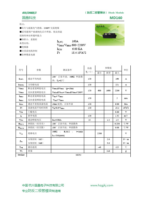
中国·杭州国晶电子科技有限公司 符号参数测试条件结温Tj (℃)参数值单位最小 典型 最大 I F(A V) 通态平均电流 180°正弦半波,50HZ 单面散热,T c =85℃ 150 160 A I F(RMS) 方均根电流150 251 A V DRM V RRM 断态重复峰值电压 反向重复峰值电压 V DRM &V RRM tp=10msV D s M &V RsM = V DRM &V RRM +200V 150 600 1600 2200 V I DRM I RRM 断态重复峰值电流 反向重复峰值电流 V DM = V DRMV RM = V RRM150 5 mA I FSM 通态不重复浪涌电流 10ms 底宽,正弦半波 150 6.00 KAI 2t 浪涌电流平均时间积 V R =0.6 V RRM 150 18.4 103A 2SV FO 门槛电压 0.80 V r F 斜率电阻150 1.35 m Ω V FM 通态峰值电压 I TM =500A25 1.2 1.3 V R th(j-c) 热阻抗(结至壳) 180°正弦半波,单面散热 0.230 ℃/W R th(c-h) 热阻抗(结至散) 180°正弦半波,单面散热 0.08 ℃/W V iso 绝缘电压 50HZ ,R.M.S ,t=1min I iso :1Ma(max) 2500 V F m 安装扭矩(M5) 安装扭矩(M6) 2.0 3.0 N ·m N ·m T sbg 储存温度 -40 125 ℃ W t 质量210gOutlineM234特点: ■芯片与底板电气绝缘,2500V 交流绝缘 ■采用德国产玻璃钝化芯片焊接,优良的温度特性和功率循环能力 ■体积小,重量轻典型应用:■变频器■交直流电机控制■各种整流电源I F(A V) 160A V DRM /V RRM 600~2200V I FSM 6.00 KA I 2t 18.4 103A 2S中国·杭州国晶电子科技有限公司中国·杭州国晶电子科技有限公司 模块典型电路 电联结形式(右图)模块外型图、安装图M234使用说明:一、使用条件及注意事项:1、使用环境应无剧烈振动和冲击,环境介质中应无腐蚀金属和破坏绝缘的杂质和气氛。
SC50VB160-G;中文规格书,Datasheet资料

MAXIMUM RATINGS AND ELECTRICAL CHARACTERISTICS
Rating at 25℃ ambient temperature unless otherwise specified. Resistive or inductive load 60Hz. For capacitive load, derate current by 20%
10
10
1.0
T J=25°C
1.0
0.1
0.1
0.01 0 20 40 60 80 100 120 140
0.01
0.4
0.6
0.8
1.0
1.2
1.4
1.6
INSTANTANEOUS FORWARD VOLTAGE,VOLTS
PERCENT OF RATED PEAK REVERSE VOLTAGE
MSD0905018A
Page 2
/
分销商库存信息:
COMCHIP SC50VB160-G
Glass Passivated 3 Phase Bridge Rectifiers
SC50VB160-G
"-G" : RoHS Device
REVERSE VOLTAGE - 1600Volts FORWARD CURRENT - 50Amperes SCVB
1.181 MAX (30.0) .252(6.4) .213(5.4) .079(2.0) .047(1.2) .354(9.0) .315(8.0) R1.75 1.417 MAX (36.0) .295(7.5) .256(6.5) .374(9.5) .334(8.5) .374(9.5) .334(8.5) .146(3.7)*45°
GB160160BNGAAMLB-V00中文资料

JEWEL HILL ELECTRONIC CO.,LTDJEWEL HILL ELECTRONIC CO.,LTD.SPECIFICATIONS FORLCD MODULEModule No. GB160160BOffice Address: Rm. 518,5/F., 101 Shangbu Industrial District,HuaqiangNorthRoad, Shenzhen, ChinaTEL : (86)-755-83362489 83617492FAX: (86)-755-83286396 83365871E-mail: sales@jhlcd@Website: TABLE OF CONTENTSLCM NUMBER SYSTEM (2)1. GENERAL DESCRIPTION (3)2. FEATURES (3)3. MECHANICAL SPECIFICATION (3)4. MECHANICAL DIMENSION (4)5. MAXIMUM RATINGS (5)6. ELECTRICAL CHARACTERISTICS (5)7. MODULE FUNCTION DESCRIPTION (6)8. ELECTRO-OPTICAL CHARACTERISTICS (13)9. RELIABILITY (17)10. PRECAUTIONS FOR USING LCD MODULES (18)11. USING LCD MODULES (20)12. REVISION HISTORY (22)SAMPLE APPROVED REPORT (23)LCM Number SystemNUMBER OF CHAR. PER LINE F: FSTN; X: OTHER VERSION NUMBER: V00~V99IC TYPE:VIEWING DIRECTION:TEMPERATURE RANGE:BACKLIGHT TYPE:SERIAL NUMBER: A~ZGRAPHIC MODULEs: NUMBER OF COMMONs GRAPHIC MODULEs:NUMBER OF SEGMENTs COB & SMT LCM BACKLIGHT COLOR:CHARACTER MODULEs:CHARACTER MODULEs: NUMBER OF LINE G: REFLECTIVE,NONE BACKLIGHT A: TRANSFLECTIVE, EL BACKLIGHT B: TRANSMISSIVE, EL BACKLIGHT C: TRANSFLECTIVE, LED BACKLIGHT D: TRANSMISSIVE, LED BACKLIGHT E: TRANSFLECTIVE, CCFL BACKLIGHT F: TRANSMISSIVE, CCFL BACKLIGHT A: AMBER; B: BLUE; Y: YELLOW-GREEN R: RED; W: WHITE; O: THER COLOR N: NORMAL TEMPERATURE RANGE U: UPPER(12:00); D: DOWN(6:00)L: LEFT(9:00); R: RIGHT(3:00);A: BONDING IC, WITH CONTROLLER B: BONDING IC, WITHOUT CONTROLLER C: SMT IC, WITH CONTROLLER D: SMT IC, WITHOUT CONTROLLER O: OTHER TYPEW: BLACK-WHITE; O: OTHER G: GRAY; Y: YELLOW-GREEN; B: BLUE; LCD COLOR MODE:N: TN; H: HTN; S: STN LCD TYPE:S: SUPER WIDE TEMPERATURE RANGE W: WIDE TEMPERATURE RANGEM: MIDDLE TEMPERATURE RANGE1. GENERAL DESCRIPTIONThe GB160160B is a 160 x 160 Dots Graphics LCD module. It has a STN panel composed of160segments and 160 commons. The LCM can be easily accessed by micro-controller via parallel interface.2. FEATURESTransflective and PositiveDisplay ModeSTN(Y-G) moduleDisplay Format Graphic 160 x 160 dotsInput Data Parallel data input from MCUMultiplexing Ratio 1/160 DutyBiasBias 1/12Viewing Direction 6 O’clock(Yellow-Green)Backlight LED3. MECHANICAL SPECIFICATIONItem Specifications Unit Dimensional outline 89.2 x 85.0 x 14.6(max) mmResolution 160segs x 160coms dotsActive area 60.775(W) x 60.775(H) mmDots pitch 0.38(W)×0.38(H) mmDots size 0.355(W)×0.355 (H) mm4. MECHANICAL DIMENSION5. MAXIMUM RATINGSItem Symbol Min Max Unit NoteV DD - V ss -0.3 5.5 V Supply voltage V LCD -0.3 24.0 V Input Voltage V IN -0.3 V DD +0.3 VOperating temperature T OPR 0 +50 Storage temperature T STR -10 +60Humidity --- --- 90 %RH6. ELECTRICAL CHARACTERISTICSItem SymbolCondition Min. Typ. Max. UnitSupply Voltage Logic V DD ------ 5.0 --- VH level V IH 0.8V DD --- V DDInput VoltageL levelV IL --- V SS --- 0.2V DDVCurrent Consumption(LCD DRIVER)I DD V DD =5.0V; V LCD =19.0V, T amb =25 ;--- --- 1.5 mALCD Driving Voltage V LCDBias=1/13V LCD =V DD -V 518.7 19.0 19.3 VCurrent Consumption (With LED BackLight)I LEDV DD =5.0V;V LED =4.2V,T amb =25 ;--- --- TBD mA7. MODULE FUNCTION DESCRIPTION7.1. PIN DESCRIPTIONINTERFACE WITH CN1 & CN2:PinSymbol Description No.1 VSSPower supply for Ground (0V)2 MAC Signal for LCD Driver Output3 FLMData Input for Common ICs4 CL1Data Latch Colok5 CL2Data Shift Colok6 D37 D2Display Data Input Terminal for Segment ICs8 D19 D010 VEE Power Supply for Negative V oltage11 VDD Power supply for positive (+5V)12 V0 VLCD V oltage Regulation Terminal13 /DISPOFF Display OFF Control14 K Power Supply for LED BackLight Negative15 A Power Supply for LED BackLight Positive7.2 TIMING CHARACTERISTICS7.3 APPLICATION OF LCMLED-LED+VDD VSS VEE V0D0-D4CL1CL2M FLMCircuit Block Diagram8. ELECTRO-OPTICAL CHARACTERISTICSItem Symbol Condition Temp Min Typ. Max UnitsNote--- 19.5 ---25 18.7 19.0 19.3 LCD driving voltageV LCD = = 050 --- 18.0 --- V NOTE1Rise Time (Tr) --- --- -- Decay Time (Tf)0 --- ---- --- Rise Time (Tr) --- 225 340Decay Time (Tf) 25 --- 240 360Rise Time (Tr) --- --- -- Response TimeDecay Time (Tf)= = 0 50 --- --- --msec NOTE2Contrast Ratio Cr= = 0 255 10 --- --- NOTE4Viewing AngleRange( = 0°)(6”) = 90°(3”) =180°(12”) =270°(9”)(25 ) CR ≥245 35 25 35DegNOTE3z For panel only․Electro-Optical Characteristics Measuring Equipment(DMS501)SystemIllumination (D65)․Note 1. Definition of Driving Voltage( Vlcd) :․Note 3. Definition of Viewing Angle and :․Note 4. Definition of Contrast ratio( CR) :Brightness of Non-selected Segment (B2)Brightness of Selected Segment (B1)CR =V,maxCR,maxDriving VoltageB r i gh t n e s s (%)Brightness Curve forSelected Segment0%=90 =270Viewing Direction 6 O’clock DirectionNormal :9. RELIABILITY9.1. MTBFThe LCD module shall be designed to meet a minimum MTBF value of 50000 hours with normal. (25°C in the room without sunlight)9.2. TESTSNO. ITEM CONDITION CRITERION 1 High Temperature Operating 50 120Hrs2 Low Temperature Operating 0 120Hrs3 High Temperature/Humidity Non-Operating50 ,90%RH ,120 Hrs4 High TemperatureNon-Operating60 120Hrs5 Low TemperatureNon-Operating-10 120Hrs6 Temperature CyclingNon-Operating 0 (30Min )↔ 50 (30Min)10 CYCLESNo Defect OfOperational Function InRoom Temperature AreAllowable.IDD of LCM inPre-and post-test shouldfollow specificationNotes: Judgments should be mode after exposure in room temperature for two hours.10. PRECAUTIONS FOR USING LCD MODULES10.1. HANDLING PRECAUTIONS(1) The display panel is made of glass. Do not subject it to a mechanical shock or impact by droppingit.(2) If the display panel is damaged and the liquid crystal substance leaks out, be sure not to get any inyour mouth. If the substance contacts your skin or clothes, wash it off using soap and water.(3) Do not apply excessive force to the display surface or the adjoining areas since this may cause thecolor tone to vary.(4) The polarizer covering the display surface of the LCD module is soft and easily scratched. Handlethis polarizer carefully.(5) If the display surface becomes contaminated, breathe on the surface and gently wipe it with a softdry cloth. If it is heavily contaminated, moisten a cloth with one of the following solvents: - Isopropyl alcohol- Ethyl alcohol(6) Solvents other than those above mentioned may damage the polarizer.Especially, do not use the following:- Water- Ketone- Aromatic solvents(7) Extra care to minimize corrosion of the electrode. Water droplets, moisture condensation or acurrent flow in a high-humidity environment accelerates corrosion of the electrode.(8) Install the LCD Module by using the mounting holes. When mounting the LCD Module, makesure it is free of twisting, warping and distortion. In particular, do not forcibly pull or bend the I/Ocable or the backlight cable.(9) Do not attempt to disassemble or process the LCD Module.(10) NC terminal should be open. Do not connect anything.(11) If the logic circuit power is off, do not apply the input signals.(12) To prevent destruction of the elements by static electricity, be careful to maintain an optimumwork environment.- Be sure to ground the body when handling he LCD Module.- Tools required for assembling, such as soldering irons, must be properly grounded.-To reduce the amount of static electricity generated, do not conduct assembling and other workunder dry conditions.-The LCD Module is coated with a film to protect the display surface. Exercise care when peeling off this protective film since static electricity may be generated.10.2. STORAGE CONDITIONSWhen storing, avoid the LCD module to be exposed to direct sunlight of fluorescent lamps. For stability, to keep it away form high temperature and high humidity environment (The best condition is : 23±5°C, 45±20%RH). ESD protection is necessary for long-term storage also.10.3. OTHERSLiquid crystals solidify under low temperature (below the storage temperature range) leading to defective orientation or the generation of air bubbles (black or white). Air bubbles may also be generated if the module is subject to a low temperature.If the LCD Module have been operating for a long time showing the same display patterns the display patterns may remain on the screen as ghost images and a slight contrast irregularity may also appear.A normal operating status can be recovered by suspending use for some time. It should be noted that this phenomenon does not adversely affect performance reliability.To minimize the performance degradation of the LCD Module resulting from destruction caused by static electricity etc. exercise care to avoid holding the following sections when handling the modules.- Exposed area of the printed circuit board.- Terminal electrode sections.11. Using LCD modules11.1 LIQUID CRYSTAL DISPLAY MODULESLCD is composed of glass and polarizer. Pay attention to the following items when handling.(1) Please keep the temperature within specified range for use and storage. Polarization degradation,bubble generation or polarizer peel-off may occur with high temperature and high humidity.(2) Do not touch, push or rub the exposed polarizers with anything harder than a HB pencil lead (glass,tweezers, etc).(3) N-hexane is recommended for cleaning the adhesives used to attach front/rear polarizers andreflectors made of organic substances, which will be damaged by chemicals such as acetone, toluene, toluene, ethanol and isopropyl alcohol.(4) When the display surface becomes dusty, wipe gently with absorbent cotton or other soft materiallike chamois soaked in petroleum ether. Do not scrub hard to avoid damaging the display surface.(5) Wipe off saliva or water drops immediately, contact with water over a long period of time maycause deformation or color fading.(6) Avoid contacting oil and fats.(7) Condensation on the surface and contact with terminals due to cold will damage, stain orpolarizers. After products are tested at low temperature they must be warmed up in a container before coming is contacting with room temperature air.(8) Do not put or attach anything on the display area to avoid leaving marks on.(9) Do not touch the display with bare hands. This will stain the display area and degrade insulationbetween terminals (some cosmetics are determinate to the polarizers).(10)As glass is fragile, it tends to become or chipped during handling especially on the edges. Pleaseavoid dropping or jarring.11.2 INSTALLING LCD MODULEAttend to the following items when installing the LCM.(1) Cover the surface with a transparent protective plate to protect the polarizer and LC cell.(2) When assembling the LCM into other equipment, the spacer to the bit between the LCM and thefitting plate should have enough height to avoid causing stress to the module surface, refer to the individual specifications for measurements. The measurement tolerance should be ±0.1mm.11.3 ELECTRO-STATIC DISCHARGE CONTROLSince this module uses a CMOS LSI, the same careful attention should be paid for electrostatic discharge as for an ordinary CMOS IC.(1) Make certain that you are grounded when handing LCM.(2) Before removing LCM from its packing case or incorporating it into a set, be sure the module andyour body have the same electric potential.(3) When soldering the terminal of LCM, make certain the AC power source for the soldering irondoes not leak.(4) When using an electric screwdriver to attach LCM, the screwdriver should be of groundpotentiality to minimize as much as possible any transmission of electromagnetic waves produced sparks coming from the commutator of the motor.(5) As far as possible, make the electric potential of your work clothes and that of the workbenches tothe ground potential.(6) To reduce the generation of electro-static discharge, be careful that the air in the work is not toodried. A relative humidity of 50%-60% is recommended.11.4 PRECAUTIONS FOR OPERATION(1) Viewing angle varies with the change of liquid crystal driving voltage (Vo). Adjust Vo to showthe best contrast.(2) Driving the LCD in the voltage above the limit will shorten its lifetime.(3) Response time is greatly delayed at temperature below the operating temperature range. However,this does not mean the LCD will be out of the order. It will recover when it returns to the specified temperature range.(4) If the display area is pushed hard during operation, the display will become abnormal. However, itwill return to normal if it is turned off and then on.(5) Condensation on terminals can cause an electrochemical reaction disrupting the terminal circuit.Therefore, this product must be used and stored within the specified condition of 23±5°C, 45±20%RH.(6) When turning the power on, input each signal after the positive/negative voltage becomes stable.11.5 SAFETY(1) It is recommended to crush damaged or unnecessary LCDs into pieces and wash them off withsolvents such as acetone and ethanol, which should later be burned.(2) If any liquid leaks out of a damaged glass cell and comes in contact with the hands, wash offthoroughly with soap and water.12. REVISION HISTORYrecord Date Version Reviseversion 06-05-241.0 Original2.0 Change contact mode 06-08-04SAMPLE APPROVED REPORT。
(优选)三相异步电动机铭牌相关参数介绍详解.

1.电机的产品型号:
1234
补充代号 特殊环境代号 规格代号 产品代号 电机型号一般由产品代号、规格代号、特殊环境 代号、补充代号等四部分组成,并按以上顺序排 列。
低压电机铭牌
高压电机铭牌
1.1 常用异步电动机的产品代号:
序号 1 2 3 4 5 6 7 8 9 10 11 12
代号 G H W F T TH TA
1.4 补充代号:用汉语拼音字母或是阿拉伯数字表示。
• 2、产品型号示例
2.1 Y KS L 1800-12/1730 -1
电机底座与泵直接连接
定子铁芯外径 极数 额定功率 立式 空-水冷却器 鼠笼转子三相立式异步电动机
备注:一期循环水泵电机,立式电机指功率,卧式电机指中心高
middle),L表示长机座(long)。铁心长度按由短至长顺序 用数字1、2、3表示。
序
系列产品
号
1 小型异步电动机
规格代号
中心高(mm)-机座长度(字母代号)-铁心长度 (数 字代号)-极数
2 中大型异步电动机 中心高(mm)-铁心长度(数字代号)- 极数
1.3 特殊环境代号
环境名称 “高”原用 “船”(海)用 户“外”用 化工防“腐”用 “热”带用 “湿热”带用 “干热”带用
和先后顺序。
5. 防护型式 IPXX (GB/T 4208 外壳防护分级(IP代码) 防护标志由字母IP和两个表示防护等级的表征数字组成。
第一位数字表示:防止人体触及或接近壳内带电部分和触及壳内 转动部件(光滑的旋转轴和类似部件除外),以及防止固体异物进入电机
(表示防尘等级)。 第二位数字表示:防止由于电机进水而引起的有害影响(表示防水等 级)。 对特殊应用和适用于规定气候条件的电机,其外壳防护等级的表
安全检测--信息技术设备

(3)带电件周围的盖板通风孔(或其它孔洞)应能防止 外物进入设备内部与带电件接触,用Φ4*100mm试验针 垂直自由通过孔洞进入机内检查;
(4)用单极插头或裸线去连接天线、地线.负载换能器或 换能器端子时,应无触电危险,用Φ1*100mm裸线插入 端子孔导套范围内检查;
插头L/N与金属外壳
插头L/N与可触及的螺 钉
(连接金属箔)
0类、0I类、III类 I类便携式 I类驻立式电动器具
0.5 0.75 3.5
I类驻立式电热器具
0.75mA或0.75mA/kW 最大不超过5mA
II类器具
0.25
电气强度
稳定性和机械危险
1.除固定式器具和手持式器具以外,打算在一个表面上的 器具,应具有足够的稳定性 。
安全检测
——信息技术设备
标准体系分类
信息技术设备的安规标准主要分为两大体系 北美体系:UL/CSA 60950-1 欧洲标准:EN60950-1, IEC60950-1 世界上绝大多数国家都借用或采用IEC的标准 例如:GB4943-2001等同于IEC60950-1999
安全的原则
信息技术设备中可能存在的危险:
提供防护限制用户接触;提供安全互锁和防护 防止维修人员的偶然接触
机械危险
设备的不稳定、尖锐边沿或拐角,用户接 触区的移动部件或危险部件可能会带来伤 害
减小机械危险的方法
限制接触 稳定性测试 警告标示 安全互锁 倒圆边沿或拐角
辐射危险
超过接受等级的辐射,用户和维修人员 应当被保护
辐射种类 激光辐射, X射线 , 紫外线辐射
(5)I类设备可触及金属件防触电处理:
基本绝缘+保护接地
DNV-OS-F101汉语版03

( 12.6)
F600 压力允许量标准,偶然压力超出设计压力不超过 10%
COOEC----安装公司工程技术中心----乔胜虎
DNV 海底管线规范 2000 版
决定壁厚地控制压力是局部的偶然压力。管道系统应当有一个压力控制系统,它能够 保证在管道的生命期内,在系统的任何一点超过局部偶然压力的概率很低。如果在偶然压力 超过设计压力达到 10%的情况下,仍能够满足上述条件,此时的管壁厚度就可以使用。
如果偶然压力不超过设计压力,比如用到了完全关断压力,偶然压力就可以减小设计 压力,参见表 3-1。
不同的系统对设计压力和偶然压力有不同的定义,比如在管道顶部和管线系统。如果 将设计压力从一个系统转换到另一个系统,转换就应当基于此压力每年超过的概率小于 10- 4 的原则。这个压力就可被定义为管道系统的偶然压力。设计压力就应当按照上述原则决定。 E300 柱形构件周围的流体速度
COOEC----安装公司工程技术中心----乔胜虎
DNV 海底管线规范 2000 版
( ) ( ) pli − pe
⋅ D − t1 ≤ 2 ⋅ t1
2 ⋅αU 3 ⋅γ m ⋅ γ sc
⋅
SMYS
−
f y,temp
( 12.1)
这个压力差是以局部偶然压力的函数给出。介绍一个荷载因子,?inc,反映了偶然压力 和设计压力的比,这个公式能够依照水面上的参考点调整,由等式(12.2)给出。
除了需要检查弹性屈曲,薄管比其它管道更易受缺陷影响。我们应当作如下特殊考虑: ——围焊和围焊处的错位 ——集中荷载,比如点支撑 如果在有效范围内证明了弹性屈曲不会发生,并且缺陷被认为是可以接受的,标准就 可以延伸到 D/t=60。 F900 局部屈曲——围焊因子 管道包括围焊的研究表明围焊对管道的压应变能力有很大的影响,参见 Ghodsi et al (1994)。当 D/t=60 时曾经发现有 40%的减少。对于 D/t 取更小的值时围焊的影响,我们 没有已知的试验数据。 有人假设这有害的效应是因为屈曲的发生,而屈曲的发生又是因为在受压边焊接的缺 陷造成的。如果这是对的话,对于较高的 D/t 值,此效应就被过于夸大了。应当用检测或者 有限元计算来得到围焊因子。 如果没有其它资料并且假定减少是由于受压边的错位,那么在 D/t=20 时,此降低就可 以忽略不记。其余的可由 D/t=60 用内插法得到。 如果没有其它的资料,下面的建议采用下面的围焊因子。
E-VAC系列中等电压真空断路器产品说明说明书

Ideal contact material and geometry ensure lowchopping current and reliable contact resistanceA few components and compact and reasonable structure ensure morereliable and safer operation Enable ideal cutoff and close of resistance, inductance load and capacitive loadSecondary plug, chassis, moving contact and grounding methods are specially designed ,completely compatible with domestically dominantmedium voltage switchgearProduct modelsE-VAC vacuum circuit breaker120E-VAC(R)i40/3150-210Voltage ratingsE: IEC/GB standardEaton circuit breaker seriesR indicates fixed type,none indicates drawout typei indicates solid-envelope d pole, none indicates assembled polerated short circuit breaking current ratedcurrentphase spacing1E-VAC series medium voltage vacuum circuit breakerProduct descriptionContentsDescription Page 156810E-VAC series medium voltage vacuum circuit breakerProduct description .................................................................Technical data ..........................................................................Dimensions .............................................................................Wiring diagram ........................................................................E-VAC series vacuum circuit breaker selection table ..............E-VAC vacuum circuit breakerProduct descriptionE-VAC Series medium voltage vacuum circuit breakers from Eaton Electrical combine our excellent vacuum technology with decades of experience in designing and manufacturing power distribution system. They offer high reliability, ease of handling and maintenance, high cost efficiency for different customers.Meet IEC, GB and DL standardsE-VAC equipped with new generation vacuum interrupter, suited fortechnologies and operation condition of power system••••••Technical featuresE-VAC utilizes mature spring operating mechanism, offers reliable and stableperformance, long service life, ease of operating,excellent corrosion protection and low maintenance within the lifetimeE-VAC adopts vertical epoxy insulation cover which can prevent harsh environment influence, making E-VAC circuit breaker suitable for various applications. Unique contact material and primary plum-shaped moving contact make E-VAC suitable for medium voltage system in various applications.E2 level electrical life extended and M2 levelmechanical life extended as per standard, capacitivecurrent breaking and making having extremelylowre-breakdown probability C2 level, having completed the type testAll products have been subject to hundreds of mechanical operation running-in tests beforeleaving the factory, ensuring the product performance in the most stable phase Utilize advanced imported testing equipment, exactly record no-load mechanical characteristics of each product, and provide users with these characteristic curves, ensure product reliability2Application conditionAmbient air temperature not exceeding 40℃, and the average value measured within 24 hours not exceeding 35℃. The minimum ambient air temperature is -15℃The effect by solar radiation can be ignoredThe ambient air is notobviously polluted by dust, smoke, corrosive orflammable gases, vapor or salt mistSeismic intensity not exceeding 8 degreeAmplitude of electromagnetic interference induced in secondary system not exceeding 1.6kV•••••••Outline dimension anddistribution panel interlocking method completelycompatible with domestically dominant medium voltage switchgear, high universality, significantly reduce design costProduct assembly utilizes tooling method to ensure dimension consistency. All products have been subject to the push panel test for standard panel, ensuringproduct interchangeability and universality•••••As the manufacturer of theworld’s first vacuum interrupter, the pioneer of vacuumtechnology, Eaton Electrical has been committed to the research, development and manufacturing of vacuum interrupters for over 70 years, and gathered plenty ofexperience. Westinghouse has become the synonym of quality and reliability.We own the world’s largest and globally leading vacuuminterrupter plant and the only vacuum interrupter plant that is equipped with large capacity high voltage laboratories.Our manufacturing capacity and design and development always maintain a leadership position.Application areasTechnology creation historyOptional accessoriesCharging handle Trolley handleLifterE-VAC series medium voltage vacuum circuit breakerProduct descriptionChemical industry Oil industry Piping industry Offshore mining ShipbuildingPaper making industry Opencast coal mine SubstationCement industry Automotive industry Power plantTextile and food industries Metallurgical industry•••••••••••••Temperature conditionThe average of relativehumidity measured within 24 hours not exceeding 95%The average vapor pressure measured within 24 hours not exceeding 2.2kPaThe average of relative humidity measured within one month not exceeding 90%The average vapor pressure measured within one month not exceeding 1.8kPa••••3E-VAC vacuum circuit breaker requires almost no relevant maintenanceIdeal for control and protection in medium voltage power supply and distribution systemSimple structure design of E-VAC vacuum circuit breaker further minimizes faultoccurrence, simplifies daily maintenance. With theindicator on the circuit breaker panel, no detection instrument is required, facilitating the judgment of working state of circuit breaker.The circuit breaker utilizes the world’s first class EatonElectrical’s vacuum interrupter with vacuum degree up to 10-6Pa, low air leakage, and ensure 50-year life with no maintenance required.The circuit breaker is equipped with superior spring charging mechanism, utilizes modular design, offering optimized mechanism main partdistribution, simpler structure and more reliable performance. The whole mechanism is composed by three modules: charging, closing, opening. Assembly and maintenance of these three parts are very simple. The spring charging mechanism composed by ratchet wheel mechanism,oscillator and closing spring is compact and smart. Theoperating mechanism is usually equipped with manual charging device and electric charging device, enabling automatic reclosing function.The circuit for manual charging operating mechanism isprovided with manual opening and closing operation buttons, circuit breaker position indicator and spring mechanism charging status indicator, switch operations counter, shunt release auxiliary switch, position and fault signals, etc..The circuit breaker of electric charging operating mechanism: added with spring charging motor, shunt release, trip free relay, and auxiliary switch for spring charging motor release.The following accessories can also be provided as needed: undervoltage release,overcurrent relay, etc..E-VAC series medium voltage vacuum circuit breakerProduct description4Main specification and technical parametersItem Unit Value Technical parameters for trip/close coilsNameParameter Note: (1)forced air cooling is required at 4000A; (2) If the user has special requirements, up to 125kA.O-0.3s-CO-180s-CO, O-180s-CO-180s-CO(50kA)5Technical dataE-VAC series medium voltage vacuum circuit breakerT echnical dataRated operating sequenceCharging duration Rated power of spring charging motor Rated voltage of spring charging motor Rated opening operating voltage Rated closing operating voltage Allowable accumulated wearingthickness of moving/fixed contact Rated short circuit current breaking cycleRated current breaking cycleMechanical lifeClosing time Opening time Secondary circuit power frequency withstand voltage (1 min)Rated short circuit making currentRated peak withstand current Rated currentRated frequency Rated lightning impulse withstand voltage (peak)Rated short-time power frequency withstand voltage (1 min)Rated voltageRated short-circuit breaking current Rated short-time withstand current (4s)Hz A kVkA kA kA kA V ms ms Cycle Cycle Cycle mm V V W s1242(phase to ground, phase to phase) 48 (gap)75 (phase to ground, phase to phase) 85(gap)506301250630 12501600 20001250 16002000 25003150 4000(1)1250 16002000 25003150 4000(1)252531.531.54040505063638080100(2)100(2)125130200020~5035~7020000, (10000 cycles at 50kA)20000, (10000 cycles at 50kA)E2(274)3AC 110/220AC 110/22065, (80W at 50kA)≤15DC 110/220V AC 110/220 DC 110/220DC 110/220Normal working voltage rangeRated working voltage (V)Rated working current of close coil (A)Rated working current of trip coil (A)AC, DC110AC, DC2202.0 1.01.80.9Closing: 80%~110% of rated working voltageOpening: 65%~120% of rated working voltage, opening will not occur when the normal working voltage is less than 30% of rated working voltageOutline and dimension of E-VAC circuit breaker (drawout type)Rated short circuit breaking current (kA)Rated current (A)Distribution panelwidth(mm)W S R N M L K J G F E D C B A H P T 6E-VAC series medium voltage vacuum circuit breakerDimensionsDimensions80080080080010001000100010001000630125016001250630125016001600~20002500~400020~31.520~4031.540(Short-circuit 125)20~31.520~4031.531.5~5031.5~50210210210275275275275275275275275275310275275275310310638638638638838838838838838652652652652852852852852852640640640640838838838838838650650650650850850850850850433433433361433433433361361626626626680626626626680680354955793549557910928028028029528028028029529559859859858659859859858658676767677767676777778787888787878888863763763769863763763769869850850850853650850850853653627727727727737737737737737740404004040400023232319313131313180010001000630~1600630~16001600~4000275275210310275275650720520720720520770770588632580580786590IIIII I 275275250252237237465455455Outline and dimension of E-VACR circuit breaker (fixed type)Note: during installation, make sure copper busbar reliably contacts the conductive surface of circuit breaker outlet in free state. Do not exert external force on the copper busbar to adjust its shape. Forced installation is not allowed!Distribution panel width Rated current (A)P H A B C E F G1\G2I J K 7E-VAC series medium voltage vacuum circuit breakerDimensionsE-VAC series medium voltage vacuum circuit breakerWiring diagramWiring diagramSecondary control connection diagram of E-VAC series vacuum circuit breaker (drawout type)The diagram shows the circuit breaker in test position, opening, discharged states8E-VAC series medium voltage vacuum circuit breakerWiring diagramSecondary control connection diagram of E-VACR series vacuum circuit breaker (fixed type) The diagram shows the circuit breaker in opening, discharged states9E-VAC series vacuum circuit breaker selection table1. Circuit breaker models2. Parameters of E-VAC series vacuum circuit breaker3. Technical parameters of spring operating mechanism4. Optional configuration (Standard option includes trip free device. Please note if the trip free device has to been canceled)E-VAC (drawout type)□E-VACR (fixed t ype)□Note: Technical parameters of products will be changed without notice. Please confirm with Eaton Corporation before ordering.10E-VAC series medium voltage vacuum circuit breakerE-VAC series vacuum circuit breaker selection tableParameters NameParameters NameName800Panel width(mm)Breaker phase spacing(mm)Rated short circuit breaking current (kA)(kA)Rated working current (A)21010002752531.540(Short-circuit 100kA )40(Short-circuit 125kA )31.54050□630□630□1250□1250□1250□1250□1600□1600□2000□1600□2000□2500□1600□2000□2500□3150□4000*□3150□4000** Forced air cooling is required at 4000AOpening power supply (V)Closing power supply (V)Spring charging motor power supply (V)□DC110□DC110□DC110□AC110□AC110□AC110□DC220□DC220□DC220□AC220□AC220□AC220□Overcurrent release □Closing latch □Position latch □Trip free relay □Undervoltage release □Operating handle□2 Overcurrent □3 Overcurrent□A□V □V □V □V□Quantity neededEaton is dedicated to ensuring that reliable, efficient and safe power is available when it’s needed most. With unparalleled knowledge of electrical power management across industries, experts at Eaton deliver customized, integrated solutions to solve our customers’ most critical challenges.Our focus is on delivering the right solution for the application. But, decision makers demand more than just innovative products. They turn to Eaton for an unwavering commitment to personal support that makes customer success a top priority. For more information,visit /seasia-electrical.Electrical Sector Asia PacificNo.3, Lane 280, Linhong Road,Changning District, ShanghaiEaton Industries Pte LtdElectrical Sector4 Loyang Lane #04-01/02Singapore 508914/seasia-electrical© 2013 Eaton Corporation All Rights Reserved Printed in SingaporeJuly 2013Eaton is a registered trademarkof Eaton Corporation.All trademarks are property of their respective owners.。
ADG1604BRUZ中文资料
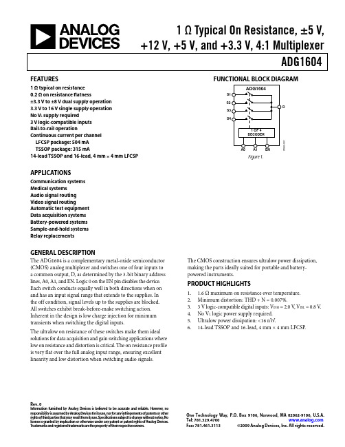
1 Ω Typical On Resistance, ±5 V,+12 V, +5 V, and +3.3 V, 4:1 MultiplexerADG1604 Rev. 0Information furnished by Analog Devices is believed to be accurate and reliable. However, noresponsibility is assumed by Analog Devices for its use, nor for any infringements of patents or other rights of third parties that may result from its use. Specifications subject to change without notice. No license is granted by implication or otherwise under any patent or patent rights of Analog Devices. T rademarks and registered trademarks are the property of their respective owners. One Technology Way, P.O. Box 9106, N orwood, MA 02062-9106, U.S.A. Tel: 781.329.4700 Fax: 781.461.3113 ©2009 Analog Devices, Inc. All rights reserved.FEATURES1 Ω typical on resistance0.2 Ω on resistance flatness±3.3 V to ±8 V dual supply operation3.3 V to 16 V single supply operationNo V L supply required3 V logic-compatible inputsRail-to-rail operationContinuous current per channelLFCSP package: 504 mATSSOP package: 315 mA14-lead TSSOP and 16-lead, 4 mm × 4 mm LFCSPAPPLICATIONSCommunication systemsMedical systemsAudio signal routingVideo signal routingAutomatic test equipmentData acquisition systemsBattery-powered systemsSample-and-hold systemsRelay replacements FUNCTIONAL BLOCK DIAGRAMD7982-1Figure 1.GENERAL DESCRIPTIONThe ADG1604 is a complementary metal-oxide semiconductor (CMOS) analog multiplexer and switches one of four inputs to a common output, D, as determined by the 3-bit binary address lines, A0, A1, and EN. Logic 0 on the EN pin disables the device. Each switch conducts equally well in both directions when on and has an input signal range that extends to the supplies. In the off condition, signal levels up to the supplies are blocked. All switches exhibit break-before-make switching action. Inherent in the design is low charge injection for minimum transients when switching the digital inputs.The ultralow on resistance of these switches make them ideal solutions for data acquisition and gain switching applications where low on resistance and distortion is critical. The on resistance profile is very flat over the full analog input range, ensuring excellent linearity and low distortion when switching audio signals. The CMOS construction ensures ultralow power dissipation, making the parts ideally suited for portable and battery-powered instruments.PRODUCT HIGHLIGHTS1. 1.6 Ω maximum on resistance over temperature.2.Minimum distortion: THD + N = 0.007%.3. 3 V logic-compatible digital inputs: V INH = 2.0 V, V INL = 0.8 V.4.No V L logic power supply required.5.Ultralow power dissipation: <16 nW.6.14-lead TSSOP and 16-lead, 4 mm × 4 mm LFCSP.ADG1604Rev. 0 | Page 2 of 20TABLE OF CONTENTSFeatures .............................................................................................. 1 Applications ....................................................................................... 1 Functional Block Diagram .............................................................. 1 General Description ......................................................................... 1 Product Highlights ........................................................................... 1 Revision History ............................................................................... 2 Specifications ..................................................................................... 3 ±5 V Dual Supply ......................................................................... 3 12 V Single Supply ........................................................................ 4 5 V Single Supply .......................................................................... 5 3.3 V Single Supply ....................................................................... 6 Continuous Current per Channel, S or D ..................................7 Absolute Maximum Ratings ............................................................8 ESD Caution...................................................................................8 Pin Configurations and Function Descriptions ............................9 Typical Performance Characteristics ........................................... 10 Test Circuits ..................................................................................... 13 Terminology .................................................................................... 16 Outline Dimensions ....................................................................... 17 Ordering Guide .. (17)REVISION HISTORY1/09—Revision 0: Initial VersionADG1604Rev. 0 | Page 3 of 20SPECIFICATIONS±5 V DUAL SUPPLYV DD = +5 V ± 10%, V SS = −5 V ± 10%, GND = 0 V , unless otherwise noted. Table 1.Parameter 25°C −40°C to +85°C −40°C to+125°C Unit Test Conditions/Comments ANALOG SWITCH Analog Signal Range V DD to V SS VOn Resistance (R ON ) 1 Ω typ V S = ±4.5 V, I S = −10 mA; see Figure 22 1.2 1.4 1.6 Ω max V DD = ±4.5 V, V SS = ±4.5 V On Resistance Match Between Channels (∆R ON ) 0.04 Ω typ V S = ±4.5 V, I S = −10 mA 0.08 0.09 0.1 Ω maxOn Resistance Flatness (R FLAT(ON)) 0.2 Ω typ V S = ±4.5 V, I S = −10 mA 0.25 0.29 0.34 Ω maxLEAKAGE CURRENTS V DD = +5.5 V, V SS = −5.5 VSource Off Leakage, I S (Off) ±0.1 nA typ V S = ±4.5 V, V D = ∓4.5 V; see Figure 23±0.2 ±1 ±8 nA max Drain Off Leakage, I D (Off)±0.1nA typV S = ±4.5V, V D = ∓4.5 V; see Figure 23±0.2 ±2 ±16 nA max Channel On Leakage, I D , I S (On) ±0.2 nA typ V S = V D = ±4.5 V; see Figure 24 ±0.4 ±2 ±16 nA max DIGITAL INPUTS Input High Voltage, V INH 2.0 V min Input Low Voltage, V INL 0.8 V max Input Current, I INL or I INH 0.005 μA typ V IN = V GND or V DD ±0.1 μA max Digital Input Capacitance, C IN 8 pF typDYNAMIC CHARACTERISTICS 1Transition Time, t TRANSITION 150 ns typ R L = 300 Ω, C L = 35 pF 278 336 376 ns max V S = 2.5 V; see Figure 29 t ON (EN) 116 ns typ R L = 300 Ω, C L = 35 pF 146 166 177 ns max V S = 2.5 V; see Figure 31 t OFF (EN) 186 ns typ R L = 300 Ω, C L = 35 pF 234 277 310 ns max V S = 2.5 V; see Figure 31 Break-Before-Make Time Delay, t D 50 ns typ R L = 300 Ω, C L = 35 pF 28.5 ns min V S1 = V S2 = 2.5 V; see Figure 30 Charge Injection 140 pC typ V S = 0 V, R S = 0 Ω, C L = 1 nF; see Figure 32 Off Isolation 70 dB typ R L = 50 Ω, C L = 5 pF, f = 1 MHz;see Figure 25Channel-to-Channel Crosstalk 70 dB typ R L = 50 Ω, C L = 5 pF, f = 1 MHz;see Figure 27Total Harmonic Distortion + Noise (THD + N) 0.007 % typ R L = 110 Ω, 5 V p-p, f = 20 Hz to 20 kHz;see Figure 28−3 dB Bandwidth 15 MHz typ R L = 50 Ω, C L = 5 pF; see Figure 26 C S (Off) 63 pF typ V S = 0 V, f = 1 MHz C D (Off) 270 pF typ V S = 0 V, f = 1 MHz C D , C S (On) 360 pF typ V S = 0 V, f = 1 MHz POWER REQUIREMENTS V DD = +5.5 V, V SS = −5.5 V I DD 0.001 μA typ Digital inputs = 0 V or V DD 1.0 μA max V DD /V SS ±3.3/±8 V min/max1Guaranteed by design, not subject to production test.ADG1604Rev. 0 | Page 4 of 2012 V SINGLE SUPPLYV DD = 12 V ± 10%, V SS = 0 V , GND = 0 V , unless otherwise noted. Table 2.Parameter 25°C −40°C to +85°C −40°C to+125°C Unit Test Conditions/Comments ANALOG SWITCH Analog Signal Range 0 V to V DD V On Resistance (R ON ) 0.95 Ω typ V S = 0 V to 10 V, I S = −10 mA; see Figure 22 1.1 1.25 1.45 Ω max V DD = 10.8 V, V SS = 0 V On Resistance Match Between Channels (∆R ON ) 0.03 Ω typ V S = 10 V, I S = −10 mA 0.06 0.07 0.08 Ω max On Resistance Flatness (R FLAT(ON)) 0.2 Ω typ V S = 0 V to 10 V, I S = −10 mA 0.23 0.27 0.32 Ω max LEAKAGE CURRENTS V DD = 13.2 V, V SS = 0 V Source Off Leakage, I S (Off) ±0.1 nA typ V S = 1 V/10 V, V D = 10 V/1 V; see Figure 23 ±0.2 ±1 ±8 nA max Drain Off Leakage, I D (Off) ±0.1 nA typ V S = 1 V/10 V, V D = 10 V/1 V; see Figure 23 ±0.2 ±2 ±16 nA max Channel On Leakage, I D , I S (On) ±0.2 nA typ V S = V D = 1 V or 10 V; see Figure 24 ±0.4 ±2 ±16 nA max DIGITAL INPUTS Input High Voltage, V INH 2.0 V min Input Low Voltage, V INL 0.8 V max Input Current, I INL or I INH 0.001 μA typ V IN = V GND or V DD ±0.1 μA max Digital Input Capacitance, C IN 8 pF typDYNAMIC CHARACTERISTICS 1Transition Time, t TRANSITION 100 ns typ R L = 300 Ω, C L = 35 pF 161 192 220 ns max V S = 8 V; see Figure 29 t ON (EN) 80 ns typ R L = 300 Ω, C L = 35 pF 95 104 111 ns max V S = 8 V; see Figure 31 t OFF (EN) 144 ns typ R L = 300 Ω, C L = 35 pF 173 205 234 ns max V S = 8 V; see Figure 31 Break-Before-Make Time Delay, t D 25 ns typ R L = 300 Ω, C L = 35 pF 18 ns min V S1 = V S2 = 8 V; see Figure 30 Charge Injection 125 pC typ V S = 6 V, R S = 0 Ω, C L = 1 nF; see Figure 32 Off Isolation 70 dB typ R L = 50 Ω, C L = 5 pF, f = 1 MHz;see Figure 25Channel-to-Channel Crosstalk 70 dB typ R L = 50 Ω, C L = 5 pF, f = 1 MHz;see Figure 27Total Harmonic Distortion + Noise 0.013 % typ R L = 110 Ω, 5 Vp-p, f = 20 Hz to 20 kHz;see Figure 28−3 dB Bandwidth 19 MHz typ R L = 50 Ω, C L = 5 pF; see Figure 26 C S (Off) 60 pF typ V S = 6 V, f = 1 MHz C D (Off) 270 pF typ V S = 6 V, f = 1 MHz C D , C S (On) 350 pF typ V S = 6 V, f = 1 MHz POWER REQUIREMENTS V DD = 12 V I DD 0.001 μA typ Digital inputs = 0 V or V DD 1 μA max I DD 230 μA typ Digital inputs = 5 V 360 μA max V DD 3.3/16 V min/max1Guaranteed by design, not subject to production test.ADG1604Rev. 0 | Page 5 of 205 V SINGLE SUPPLYV DD = 5 V ± 10%, V SS = 0 V , GND = 0 V , unless otherwise noted. Table 3.Parameter 25°C −40°C to +85°C −40°C to+125°C Unit Test Conditions/Comments ANALOG SWITCH Analog Signal Range 0 V to V DD V On Resistance (R ON ) 1.7 Ω typ V S = 0 V to 4.5 V, I S = −10 mA; see Figure 22 2.15 2.4 2.7 Ω max V DD = 4.5 V, V SS = 0 V On Resistance Match Between Channels (∆R ON ) 0.05 Ω typ V S = 0 V to 4.5 V, I S = −10 mA 0.09 0.12 0.15 Ω max On Resistance Flatness (R FLAT(ON)) 0.4 Ω typ V S = 0 V to 4.5 V, I S = −10 mA 0.53 0.55 0.6 Ω max LEAKAGE CURRENTS V DD = 5.5 V, V SS = 0 V Source Off Leakage, I S (Off) ±0.05 nA typ V S = 1 V/4.5 V, V D = 4.5 V/1 V; see Figure 23 ±0.2 ±1 ±8 nA max Drain Off Leakage, I D (Off) ±0.05 nA typ V S = 1 V/4.5 V, V D = 4.5 V/1 V; see Figure 23 ±0.2 ±2 ±16 nA max Channel On Leakage, I D , I S (On) ±0.1 nA typ V S = V D = 1 V or 4.5 V; see Figure 24 ±0.4 ±2 ±16 nA max DIGITAL INPUTS Input High Voltage, V INH 2.0 V min Input Low Voltage, V INL 0.8 V max Input Current, I INL or I INH 0.001 μA typ V IN = V GND or V DD ±0.1 μA max Digital Input Capacitance, C IN 8 pF typ DYNAMIC CHARACTERISTICS 1 Transition Time, t TRANSITION 175 ns typ R L = 300 Ω, C L = 35 pF 283 337 380 ns max V S = 2.5 V; see Figure 29 t ON (EN) 135 ns typ R L = 300 Ω, C L = 35 pF 174 194 212 ns max V S = 2.5 V; see Figure 31 t OFF (EN) 228 ns typ R L = 300 Ω, C L = 35 pF 288 342 385 ns max V S = 2.5 V; see Figure 31 Break-Before-Make Time Delay, t D 30 ns typ R L = 300 Ω, C L = 35 pF 21 ns min V S1 = V S2 = 2.5 V; see Figure 30 Charge Injection 70 pC typ V S = 2.5 V, R S = 0 Ω, C L = 1 nF; see Figure 32 Off Isolation 70 dB typ R L = 50 Ω, C L = 5 pF, f = 100 kHz;see Figure 25Channel-to-Channel Crosstalk 70 dB typ R L = 50 Ω, C L = 5 pF, f = 100 kHz;see Figure 27Total Harmonic Distortion + Noise 0.09 % typ R L = 110 Ω, f = 20 Hz to 20 kHz, V S = 3.5 V p-p;see Figure 28−3 dB Bandwidth 16 MHz typ R L = 50 Ω, C L = 5 pF; see Figure 26 C S (Off) 70 pF typ V S = 2.5 V, f = 1 MHz C D (Off) 300 pF typ V S = 2.5 V, f = 1 MHz C D , C S (On) 400 pF typ V S = 2.5 V, f = 1 MHz POWER REQUIREMENTS V DD = 5.5 V I DD 0.001 μA typ Digital inputs = 0 V or V DD 1 μA max V DD 3.3/16 V min/max1Guaranteed by design, not subject to production test.ADG1604Rev. 0 | Page 6 of 203.3 V SINGLE SUPPLYV DD = 3.3 V , V SS = 0 V , GND = 0 V , unless otherwise noted. Table 4.Parameter 25°C −40°C to +85°C −40°C to+125°C Unit Test Conditions/Comments ANALOG SWITCH Analog Signal Range 0 V to V DD V On Resistance (R ON ) 3.2 Ω typ V S = 0 V to V DD , I S = −10 mA; see Figure 22 3.6 3.8 4 Ω max V DD = 3.3 V, V SS = 0 V On Resistance Match Between Channels (∆R ON ) 0.06 Ω typ V S = 0 V to V DD , I S = −10 mA 0.15 0.16 0.17 Ω max On Resistance Flatness (R FLAT(ON)) 1.2 Ω typ V S = 0 V to V DD , I S = −10 mA 1.6 1.7 1.8 Ω max LEAKAGE CURRENTS V DD = 3.6 V, V SS = 0 V Source Off Leakage, I S (Off) ±0.02 nA typ V S = 0.6 V/3 V, V D = 3 V/0.6 V; see Figure 23 ±0.25 ±1 ±8 nA max Drain Off Leakage, I D (Off) ±0.02 nA typ V S = 0.6 V/3 V, V D = 3 V/0.6 V; see Figure 23 ±0.25 ±2 ±16 nA max Channel On Leakage, I D , I S (On) ±0.05 nA typ V S = V D = 0.6 V or 3 V; see Figure 24 ±0.6 ±2 ±16 nA max DIGITAL INPUTS Input High Voltage, V INH 2.0 V min Input Low Voltage, V INL 0.8 V max Input Current, I INL or I INH 0.001 μA typ V IN = V GND or V DD ±0.1 μA max Digital Input Capacitance, C IN 8 pF typ DYNAMIC CHARACTERISTICS 1 Transition Time, t TRANSITION 280 ns typ R L = 300 Ω, C L = 35 pF 460 526 575 ns max V S = 1.5 V; see Figure 29 t ON (EN) 227 ns typ R L = 300 Ω, C L = 35 pF 308 332 346 ns max V S = 1.5 V; see Figure 31 t OFF (EN) 357 ns typ R L = 300 Ω, C L = 35 pF 480 549 601 ns max V S = 1.5 V; see Figure 31 Break-Before-Make Time Delay, t D 25 ns typ R L = 300 Ω, C L = 35 pF 20 ns min V S1 = V S2 = 1.5 V; see Figure 30 Charge Injection 60 pC typ V S = 1.5 V, R S = 0 Ω, C L = 1 nF; see Figure 32 Off Isolation 70 dB typ R L = 50 Ω, C L = 5 pF , f = 100 kHz;see Figure 25Channel-to-Channel Crosstalk 70 dB typ R L = 50 Ω, C L = 5 pF, f = 100 kHz;see Figure 27Total Harmonic Distortion + Noise 0.15 % typ R L = 110 Ω, f = 20 Hz to 20 kHz, V S = 2 V p-p;see Figure 28−3 dB Bandwidth 15 MHz typ R L = 50 Ω, C L = 5 pF; see Figure 26 C S (Off) 76 pF typ V S = 1.5 V, f = 1 MHz C D (Off) 316 pF typ V S = 1.5 V, f = 1 MHz C D , C S (On) 420 pF typ V S = 1.5 V, f = 1 MHz POWER REQUIREMENTS V DD = 3.6 V I DD 0.001 μA typ Digital inputs = 0 V or V DD 1.0 1.0 μA max V DD 3.3/16 V min/max1Guaranteed by design, not subject to production test.ADG1604Rev. 0 | Page 7 of 20CONTINUOUS CURRENT PER CHANNEL, S OR DTable 5.Parameter 25°C 85°C 125°C Unit CONTINUOUS CURRENT, S OR D V DD = +5 V, V SS = −5 V TSSOP (θJA = 150.4°C/W) 315 189 95 mA maximum LFCSP (θJA = 48.7°C/W) 504 259 112 mA maximum V DD = 12 V, V SS = 0 V TSSOP (θJA = 150.4°C/W) 378 221 112 mA maximum LFCSP (θJA = 48.7°C/W) 627 311 126 mA maximum V DD = 5 V, V SS = 0 V TSSOP (θJA = 150.4°C/W) 249 158 91 mA maximum LFCSP (θJA = 48.7°C/W) 403 224 105 mA maximum V DD = 3.3 V, V SS = 0 V TSSOP (θJA = 150.4°C/W) 256 165 98 mA maximum LFCSP (θJA = 48.7°C/W) 410 235 116 mA maximumADG1604Rev. 0 | Page 8 of 20ABSOLUTE MAXIMUM RATINGST A = 25°C, unless otherwise noted.Stresses above those listed under Absolute Maximum Ratings may cause permanent damage to the device. This is a stress rating only; functional operation of the device at these or any other conditions above those indicated in the operationalsection of this specification is not implied. Exposure to absolute maximum rating conditions for extended periods may affect device reliability. Table 6.Parameter Rating V DD to V SS 18 V V DD to GND −0.3 V to +18 V V SS to GND +0.3 V to −18 V Analog Inputs 1 V SS − 0.3 V to V DD + 0.3 V or30 mA, whichever occurs firstDigital Inputs 1GND − 0.3 V to V DD + 0.3 V or30 mA, whichever occurs firstPeak Current, S or D 1150 mA (pulsed at 1 ms,10% duty cycle maximum)Continuous Current, S or D 2 Data + 15% Operating Temperature Range Industrial (Y Version) −40°C to +125°C Storage Temperature Range −65°C to +150°C Junction Temperature 150°C16-Lead TSSOP , θJA ThermalImpedance (2-Layer Board)150.4°C/W 16-Lead LFCSP , θJA ThermalImpedance (4-Layer Board)48.7°C/W Reflow Soldering PeakTemperature, Pb free260°CESD CAUTION1Overvoltages at IN, S, or D are clamped by internal diodes. Current should be limited to the maximum ratings given. 2SeeTable 5.ADG1604Rev. 0 | Page 9 of 20PIN CONFIGURATIONS AND FUNCTION DESCRIPTIONSNC = NO CONNECTENV SS S1NCD S2A0GND V DD S3NCNCS4A107982-002Figure 2. 14-Lead TSSOP Pin Configuration07982-003NOTES1. NC = NO CONNECT.2. EXPOSED PAD TIED TO SUBSTRATE, V SS .1V SS 2NC 3S14S211V DD 12GND 10S39S45N C 6D 7N C 8N C 15A 016E N14A 113N CFigure 3. 16-Lead LFCSP Pin ConfigurationTable 7. Pin Function DescriptionsPin No.Mnemonic Description TSSOP LFCSP 1 15 A0 Logic Control Input. 2 16 EN Active High Digital Input. When this pin is low, the device is disabled and all switches areoff. When this pin is high, the Ax logic inputs determine the on switch.3 1 V SS Most Negative Power Supply Potential.4 3 S1 Source Terminal. This pin can be an input or output.5 4 S2 Source Terminal. This pin can be an input or output.6 6 D Drain Terminal. This pin can be an input or output. 7, 8, 9 2, 5, 7, 8, 13 NC No Connection. 10 9 S4 Source Terminal. This pin can be an input or output. 11 10 S3 Source Terminal. This pin can be an input or output. 12 11 V DD Most Positive Power Supply Potential. 13 12 GND Ground (0 V) Reference. 14 14 A1 Logic Control Input. N/A 17 (EPAD) EP (EPAD) Exposed Pad. Tied to substrate, V SS .Table 8. ADG1604 Truth TableE NA1 A0 S1 S2 S3 S4 0 X X Off Off Off Off 1 0 0 On Off Off Off 1 0 1 Off On Off Off 1 1 0 Off Off On Off 1 1 1 Off Off Off OnADG1604Rev. 0 | Page 10 of 20TYPICAL PERFORMANCE CHARACTERISTICS0.40.60.81.01.21.4–8–6–4–202468O N R E S I S T A N C E (Ω)V S OR V D VOLTAGE (V)07982-014Figure 4. On Resistance as a Function of V D (V S ) for Dual Supply0.51.01.52.02.53.03.50246810121416O N R E S I S T A N C E (Ω)V S OR V D VOLTAGE (V)07982-015Figure 5. On Resistance as a Function of V D (V S ) for Single Supply0.40.60.81.01.21.4–6–4–2246O N R E S I S T A N C E(Ω)V S OR V D VOLTAGE (V)07982-012Figure 6. On Resistance as a Function of V D (V S ) for Different Temperatures,±5 V Dual Supply 0.40.60.81.01.21.4024681012O N R E S I S T A N C E (Ω)V S OR V D VOLTAGE (V)07982-010Figure 7. On Resistance as a Function of V D (V S ) for Different Temperatures,12 V Single Supply1.01.52.02.500.5 1.0 1.5 2.0 2.5 3.0 3.5 4.0 4.5 5.0O N R E S I S T A N C E (Ω)V S OR V D VOLTAGE (V)07982-013Figure 8. On Resistance as a Function of V D (V S ) for Different Temperatures,5 V Single Supply1.52.02.53.03.54.000.5 1.0 1.5 2.0 2.5 3.0 3.5O N R E S I S T A N C E (Ω)V S OR V D VOLTAGE (V)07982-006Figure 9. On Resistance as a Function of V D (V S ) for Different Temperatures,3.3 V Single Supply07982-033TEMPERATURE (°C)–15–10–551015L E A K A G E C U R R E N T (n A )20406080100120Figure 10. Leakage Currents as a Function of Temperature, ±5 V Dual Supply07982-032TEMPERATURE (°C)L E A K A G E C U R R E N T (n A )–15–10–505101520 Figure 11. Leakage Currents as a Function of Temperature, 12 V Single Supply07982-030–5510152020406080100120L E A K A G E C U R R E N T (n A )TEMPERATURE (°C)Figure 12. Leakage Currents as a Function of Temperature, 5 V Single Supply 07982-03120406080100120TEMPERATURE (°C)–4–2024681012141618L E A K A G E C U R R E N T (n A )Figure 13. Leakage Currents as a Function of Temperature, 3.3 V Single Supply–100010*******400500600I D D (µA )24681012LOGIC (V)07982-005Figure 14. I DD vs. Logic Level050100150200250300350–6–4–22468101214C H A R G E I N J E C T I O N (p C )V S (V)07982-009Figure 15. Charge Injection vs. Source Voltage50100150200250300350400450–40–20020406080100120T I M E (n s )TEMPERATURE (°C)07982-019Figure 16. t ON /t OFF Times vs. Temperature–110–105–100–95–90–85–80–75–70–65–60–55–50–45–40–35–30–25–20–15O F F I S O L A T I O N (d B )FREQUENCY (Hz)100k 1M 10M 100M 1G10k1k 07982-007Figure 17. Off Isolation vs. Frequency–120–100–80–60–40–20C R O S S T A L K (d B )FREQUENCY (Hz)100k 1M 10M 100M 1G10k 1k07982-018Figure 18. Crosstalk vs. FrequencyI N S E R T I O N L O S S (d B )FREQUENCY (Hz)100k 1M 10M 100M10k 1k–6–5–3–1–4–207982-004Figure 19. On Response vs. Frequency–100–90–80–70–60–50–40–30–20–100FREQUENCY (Hz)100k1M10M10k1kA C P S R R (dB )07982-008Figure 20. ACPSRR vs. Frequency00.020.040.060.080.100.120.140.160.180.20T H D + N (%)FREQUENCY (Hz)15k 10k5k 20k07982-017Figure 21. THD + N vs. FrequencyTEST CIRCUITSV 07982-020Figure 22. On ResistanceV S07982-021Figure 23. Off Leakage07982-022Figure 24. On LeakageOFF ISOLATION = 20 logOUT V S07982-027Figure 25. Off IsolationINSERTION LOSS = 20 logV OUT WITHOUT SWITCH07982-028Figure 26. BandwidthCHANNEL-TO-CHANNEL CROSSTALK = 20 logV OUT L ΩV S07982-029Figure 27. Channel-to-Channel Crosstalk07982-034Figure 28. THD + NoiseV INV OUTADDRESS DRIVE (V IN )V OUT07982-023Figure 29. Address to Output Switching TimesADDRESS DRIVE (V IN )VOUTV INV OUT0V3V 07982-024Figure 30. Break-Before-Make Time DelayENABLE DRIVE (V IN )V OUTV INOUTPUTV07982-025Figure 31. Enable-to-Output Switching DelayENOUTV OUTV INV 07982-026Figure 32. Charge InjectionTERMINOLOGYI DDThe positive supply current.I SSThe negative supply current.V D (V S)The analog voltage on Terminal D and Terminal S.R ONThe ohmic resistance between Terminal D and Terminal S.R FLAT(ON)Flatness that is defined as the difference between the maximum and minimum value of on resistance measured over the specified analog signal range.I S (Off)The source leakage current with the switch off.I D (Off)The drain leakage current with the switch off.I D, I S (On)The channel leakage current with the switch on.V INLThe maximum input voltage for Logic 0.V INHThe minimum input voltage for Logic 1.I INL (I INH)The input current of the digital input.C S (Off)The off switch source capacitance, which is measured with reference to ground.C D (Off)The off switch drain capacitance, which is measured with reference to ground.C D, C S (On)The on switch capacitance, which is measured with reference to ground.C INThe digital input capacitance. t TRANSITIONThe delay time between the 50% and 90% points of the digital input and switch on condition when switching from one address state to another.t ON (EN)The delay between applying the digital control input and the output switching on. See Figure 31.t OFF (EN)The delay between applying the digital control input and the output switching off. See Figure 31.Charge InjectionA measure of the glitch impulse transferred from the digital input to the analog output during switching.Off IsolationA measure of unwanted signal coupling through an off switch. CrosstalkA measure of unwanted signal that is coupled through from one channel to another as a result of parasitic capacitance. BandwidthThe frequency at which the output is attenuated by 3 dB.On ResponseThe frequency response of the on switch.Insertion LossThe loss due to the on resistance of the switch.Total Harmonic Distorition + Noise (THD + N)The ratio of the harmonic amplitude plus noise of the signal to the fundamental.AC Power Supply Rejection Ratio (ACPSRR)The ratio of the amplitude of signal on the output to the amplitude of the modulation. This is a measure of the ability of the part to avoid coupling noise and spurious signals that appear on the supply voltage pin to the output of the switch. The dc voltage on the device is modulated by a sine wave of 0.62 V p-p.OUTLINE DIMENSIONSCOMPLIANT TO JEDEC STANDARDS MO-153-AB-1061908-A0.300.191.050.750.600.45COPLANARITY0.10Figure 33. 14-Lead Thin Shrink Small Outline Package [TSSOP](RU-14)Dimensions shown in millimetersCOMPLIANT TO JEDEC STANDARDS MO-220-VGGC.0.500.40COPLANARITY0.081.000.850.800.18031006-AFOR PROPER CONNECTION OFTHE EXPOSED PAD, REFER TO THE PIN CONFIGURATION AND FUNCTION DESCRIPTIONSSECTION OF THIS DATA SHEET.Figure 34. 16-Lead Lead Frame Chip Scale Package [LFCSP_VQ] 4 mm × 4 mm Body, Very Thin Quad(CP-16-13)Dimensions shown in millimetersORDERING GUIDEModel Temperature Range Package Description Package OptionADG1604BRUZ 1 −40°C to +125°C 14-Lead Thin Shrink Small Outline Package [TSSOP] RU-14 ADG1604BRUZ-REEL 1 −40°C to +125°C 14-Lead Thin Shrink Small Outline Package [TSSOP]RU-14 ADG1604BRUZ-REEL71−40°C to +125°C 14-Lead Thin Shrink Small Outline Package [TSSOP] RU-14 ADG1604BCPZ- REEL 1 −40°C to +125°C 16-Lead Lead Frame Chip Scale Package [LFCSP_VQ]CP-16-13 ADG1604BCPZ-REEL71−40°C to +125°C 16-Lead Lead Frame Chip Scale Package [LFCSP_VQ]CP-16-131Z = RoHS Compliant Part.NOTESNOTESNOTES©2009 Analog Devices, Inc. All rights reserved. Trademarks andregistered trademarks are the property of their respective owners.D07982-0-1/09(0)。
DX60系列电子进气阀说明书

General Maintenance
To ensure proper operation of your Dixon® valve, proper maintenance must be performed at regular intervals. To prevent damage, check all fitting connections and screw connections for any loosening of the connections during equipment operation. Maintain adequate spare parts stock for all replacement components on the piece of equipment. Please refer to the repair kits section of the manual for complete component part numbers and kit part numbers.
use cleaning agents that will attack stainless-steel or the elastomers that were supplied with the valve. If you are unsure what elastomer is used in the valve, reference the part number key in this manual to make the determination. Follow any MSDS instructions for proper use or handling of cleaning agents. Flush the equipment sufficiently to remove any soiling from the product contact components. Depending on the process, there may be varying amounts of soiling. Cleaning times and cleaning agent concentrations will vary depending on the product being processed. It is the responsibility of the operator to determine and adjust these cleaning specifications as necessary. The equipment should not be allowed to sit with product present in it for extended periods of time. Equipment should be cleaned immediately after processing is complete.
电磁保护设备TeSys GV系列产品参数表说明书
C i r c u i t b r e a k e r sCircuit breakersTeSys GV, GBC ontrol and P rotection C omponentsChapterB60.75g g 1.1g g 1.5375 2.533.5 LR2 K0308GV2LE071.1g g –––––– 2.533.5 LR2 K0308GV2LE071.5g g 1.5g g 3375451 LR2 K0310GV2LE08––– 2.2g g –––451 LR2 K0312GV2LE082.2g g 3501004375 6.378 LR2 K0312GV2LE103g g 410100 5.537510138 LR2 K0314GV2LE144g g 5.510100–––10138 LR2 K0316GV2LE14––––––7.537510138 LRD 14GV2LE14––––––937514170 LRD 16GV2LE165.515507.56751137514170 LR2 K0321GV2LE167.5155096751537518223 LRD 21GV2LE20915401147518.537525327 LRD 22GV2LE2211154015475–––25327 LRD 22GV2LE2215105018.54752237532416LRD 32GV2LE32(1) As % of Icu.g ) > 100 kA.GV2 LE10D F 526144.t i fC i r c u i t b r e a k e r s0.09––––––0.45LRD 03GV2L030.12g g –––0.37g g 0.638LRD 04GV2L040.18g g ––––––0.638LRD 04GV2L04––––––0.55g g 113LRD 05GV2L050.25g g ––––––113LRD 05GV2L05––––––0.75g g 113LRD 06GV2L050.37g g 0.37g g –––113LRD 05GV2L050.55g g 0.55g g 1.1g g 1.622.5LRD 06GV2L06–––0.75g g ––– 1.622.5LRD 06GV2L060.75g g 1.1g g 1.54100 2.533.5LRD 07GV2L07Example: GV3 L32 becomes GV3 L326.(1) As % of Icu. Associated current limiter or fuses, where required. See characteristics page B6/33.g > 100 kA.GV2 L10D F 526145.t i fGV3 L65D F 526146.t i fTeSys GVThermal-magnetic motor circuit breakers GV2 ME0.06gg––––––0.16…0.252.4GV2ME020.09g g––––––0.25…0.405GV2ME030.12 0.18g g g g – –– –– – 0.37 –g–g –0.40…0.638GV2ME040.25gg––– 0.55gg0.63…113GV2ME050.37 0.55 –g g –g g –0.37 0.55 0.75g g g g g g – 0.75 1.1– g g – g g 1…1622.5GV2ME060.75g g1.1gg1.5375 1.6...2.533.5GV2ME071.1 1.5g g g g 1.5 2.2g g g g 2.2 3 3 375 75 2.5 (4)51GV2ME082.2gg350100 43754...6.378GV2ME103 4g g g g 4 5.510 10100 100 5.5 7.5 3 375 756 (10)138GV2ME145.5 –15 –50 –7.5 – 6 –75 – 9 11 3 375 759…14170GV2ME167.5155096751537513…18223GV2ME209154011475 18.537517…23327GV2ME2111154015475 –––20…25327GV2ME22 (3)15105018.54752237524 (32)416GV2ME32Motor circuit breakers from 0.06 to 15 kW / 400 V, with lugsTo order thermal magnetic circuit breakers with connection by lugs, add the digit 6 to the end of reference selected above.Example: GV2 ME08 becomes GV2 ME086.Thermal magnetic circuit breakers GV2 ME with built-in auxiliary contact block With instantaneous auxiliary contact block (composition, see page B6/11):b GV AE1, add suffix AE1TQ to the motor circuit breaker reference selected above. Example: GV2 ME01AE1TQ .b GV AE11, add suffix AE11TQ to the motor circuit breaker reference selected above. Example: GV2 ME01AE11TQ .b GV AN11, add suffix AN11TQ to the motor circuit breaker reference selected above. Example: GV2 ME01AN11TQ .These circuit breakers with built-in contact block are sold in lots of 20 units in a single pack.(1) As % of Icu.(2) The thermal trip setting must be within the range marked on the graduated knob.(3) Maximum rating which can be mounted in enclosures GV2 MC or MP , please consult your Regional Sales Office. g > 100 kA.GV2 ME10D F 526134.t i fC i r c u i t b r e a k e r sTeSys GVTeSys protection componentsThermal-magnetic motor circuit breakers GV2 MEReferences0.06g g ––– 0.16…0.25 2.4GV2ME0230.09g g ––– 0.25…0.405GV2ME0330.120.18g g g g –––0.40…0.638GV2ME0430.250.37g g g g 0.37g g 0.63…113GV2ME0530.370.55g g g g 0.370.550.75g g g g g g 1…1.622.5GV2ME0630.75g g1.1g g 1.6…2.533.5GV2ME0731.11.5g g g g 1.52.2g g g g 2.5…451GV2ME0832.2g g 350100 4…6.378GV2ME10334g g g g 45.510101001006…10138GV2ME1435.515507.5675 9…14170GV2ME1637.515509675 13…18223GV2ME203911151540401147517…23327GV2ME2131115401547520 (25)327GV2ME223Contact blocksDescription Mounting Maximum number Type of contacts Sold in lots of Unitreference Instantaneous auxiliary contactsFront 1N/O + N/C 10GVAE113N/O + N/O 10GVAE203LH side2N/O + N/C 1GVAN113N/O + N/O1GVAN203AccessoryDescriptionApplicationSold in lots of Unitreference Cable end reducerFor connection of conductors from 1 to 1.5 mm 220LA9D99(1) For connection of conductors from 1 to 1.5 mm 2, the use of an LA9 D99 cable end reducer is recommended.(2) Maximum rating which can be mounted in enclosures GV2 MC or MP , please consult your Regional Sales Office (3) The thermal trip setting must be within the range marked on the graduated knob.g > 100 kA.GV2 ME pp 3D F 526135.t i fLA9 D99D F 533898.e p sTeSys GVReferencesTeSys protection componentsThermal-magnetic motor circuit breakersGV2 P, GV3 P and GV3 ME80GV2 P10D F 526137.t i fGV3 P65D F 526139.t i fGV3 P651D F 526140.t i fC i r c u i t b r e a k e r sTeSys GVReferences93610011181001581007.59707010010091150501001001115101010010012…20GV7RS20 2.0109113636100100111518181001001518.58810010015…25GV7RE25 2.0109117070100100111550501001001518.5101010010015…25GV7RS25 2.01018.53610018.522181810010022810025…40GV7RE40 2.01018.57010018.550100221010025…40GV7RS40 2.0102236100301810030810030…50GV7RE50 2.01522701003050100301010030 (50)GV7RS502.01537361004555181810010055810048...80GV7RE80 2.040377010045555050100100551010048...80GV7RS80 2.0404536100–1810075810060...100GV7RE100 2.0404570100–50100751010060...100GV7RS100 2.0405575353510010075903030100100901108810010090 (150)GV7RE1502.020557570701001007590505010010090110101010010090…150GV7RS150 2.02090110353510010011013216030303010010010016020088100100132…220GV7RE220 2.3509011070701001001101321605050501001001001602001010100100132…220GV7RS220 2.350(1) As % of lcu.TeSys protection componentsThermal-magnetic motor circuit breakers GV7 RGV7 RE40D F 526138.t i fGV7 RS220D F 526141.t i f0.12–0.120.180.18–0.370.40…0.6313GV2RT040.090.120.250.370.250.370.370.550.63…122GV2RT050.180.250.370.550.370.550.370.550.750.751.11…1.633GV2RT060.370.750.751.1 1.11.51.6…2.551GV2RT070.550.75 1.11.5 1.51.52.2 2.23 2.5…478GV2RT081.12.22.23344…6.3138GV2RT101.52.234445.5 5.57.56…10200GV2RT142.23 5.55.57.57.59119…14280GV2RT1647.57.5991513…18400GV2RT205.5911111118.517…23400GV2RT21(1) The thermal trip setting must be within the range marked on the graduated knob.GV2 RTD F 526142.t i fC i r c u i t b r e a k e r sblack handle, blue legend plate(1) The thermal trip setting must be within the range marked on the graduated knob.(2) Other accessories such as mounting, cabling and marking accessories are identical to those used for GV2 ME motor circuit breakers, see page B6/13.GV2 RTD F 526142.t i fD F 526340.e p sC i r c u i t b r e a k e r sTeSys GVDescription Mounting Maximum number Type of contacts Sold inlots of Unitreference Instantaneous auxiliary contactsFront (1)1N/O or N/C (2)10GVAE1N/O + N/C 10GVAE11N/O + N/O10GVAE20Side (LH)2N/O + N/C1GVAN11N/O + N/O1GVAN20Fault signalling contact + instantaneous auxiliary contact Side (3) (LH)1N/O (fault)+ N/O1GVAD1010+ N/C1GVAD1001N/C (fault)+ N/O1GVAD0110+ N/C1GVAD0101Short-circuit signalling contactSide (LH)1C/O common point1GVAM11(1 block on RH sideof circuit breaker GV2 ME)50 Hz GVAX11560 Hz GVAX116127 V60 Hz GVAX115220…240 V 50 Hz GVAX22560 Hz GVAX226380…400 V50 Hz GVAX38560 Hz GVAX386415…440 V 50 Hz GVAX415440 V60 Hz GVAX385Add-on contact blocksDescriptionMountingMaximum number Reference Visible isolation block (5)Front (1)1GV2AK00 (6)LimitersAt top(GV2 ME and GV2 P)1GV1L3Independent1LA9LB920(1) Mounting of a GV AE contact block or a GV2 AK00 visible isolation block on GV2 P and GV2 L .(2) Choice of N/C or N/O contact operation, depending on which way round the reversible block is mounted.(3) The GV AD is always mounted next to the circuit breaker.(4) To order an undervoltage trip: replace the dot (p ) in the reference with a U , example: GV AU025. To order a shunt trip: replace the dot (p ) in the reference with an S , example: GV AS025.(5) Visible isolation of the 3 poles upstream of circuit breaker GV2 P and GV2 L .Visible isolation block GV2 AK00 cannot be used with motor circuit breakers GV2 P32 and GV2 L32 (Ith max = 25 A).(6) Ie Max = 32 A.ReferencesTeSys protection componentsThermal-magnetic and magnetic motor circuit breakers GV2 with screw clamp connectionsAdd-on blocks and accessoriesCharacteristics:pages B6/89 and B6/94Dimensions, schemes:pages B6/70 to B6/82LA9LB920D B 126629.e p sC i r c u i t b r e a k e r sTeSys GVTerminal blockfor supply to one or more GV2 G busbar setsConnection from the top1GV1G09Can be fitted with current limiter GV1 L3 (GV2 ME and GV2 P)1GV2G05Cover for terminal block For mounting in modular panels10LA9E07Flexible 3-pole connection for connecting a GV2 to a contactor LC1-D09…D25 Centre distance between mounting rails: 100…120 mm10GV1G02Set of connections upstream/downstream For connecting GV2 ME to a printed circuit board 10GV2GA01“Large Spacing” adapter UL 508 type EFor GV2 P pp H7 (except 32 A)1GV2GH7Clip-in marker holders (supplied with each circuit breaker)For GV2 P , GV2 L, GV2 LE and GV2 RT (8 x 22 mm)100LA9D92ReferencesTeSys protection componentsThermal-magnetic and magnetic motor circuit breakers GV2 with screw clamp connectionsAccessoriesDimensions, schemes:pages B6/70 to B6/82D B 417942.e p sTeSys GVD B 126631.e p sD B 126630.e p sD B 126632.e p s7P B 106297_45.e p sExtended Rotary HandleAllows a circuit breaker or a starter-controller installed in back of an enclosure to be operated from the front of the enclosure.A rotary handle can be black or red/yellow, IP54 or IP65. It includes a function for locking the circuit breaker or the starter in the O (Off) or I (On) position(depending of the type of rotary handle) by means of up to 3 padlocks with a shank diameter of 4 to 8 mm. The extended shaft must be adjusted to use in different size enclosures. The IP54 rotary handle is fixed with a nut (Ø22) to make easierthe assembling. The new Laser Square tool brings the accuracy to align the circuit breaker and the rotary handle.device(padlocks not included)ReferencesTeSys protection componentsThermal-magnetic and magnetic motor circuit breakers GV2 with screw clamp connectionsC i r c u i t b r e a k e r sTeSys GVDescriptionMounting Maximum number Type of contacts Sold inlots of Unitreference Instantaneous auxiliary contactsFront1N/O or N/C (1)10GVAE1N/O + N/C 10GVAE11 (2)N/O + N/O10GVAE20 (2)Side (LH)2N/O + N/C1GVAN11 (2)N/O + N/O1GVAN20 (2)Fault signalling contact + instantaneous auxiliary contactFront 1N/O (fault)+ N/O1GVAED101 (2)N/O (fault)+ N/C1GVAED011 (2)Side (3) (LH)1N/O (fault)+ N/O1GVAD1010+ N/C1GVAD1001N/C (fault)+ N/O1GVAD0110+ N/C1GVAD0101Short-circuit signalling contact Side (LH)1C/O common point 1GVAM11(4)MountingVoltage ReferenceSide(1 block on RH side of circuit breaker)24 V 50 Hz GVA p 02560 Hz GVA p 02648 V 50 Hz GVA p 05560 Hz GVA p 05610050 Hz GVA p 107100…110 V 60 Hz GVA p 107110…115 V 50 Hz GVA p 11560 Hz GVA p 116120…127 V 50 Hz GVA p 125127 V 60 Hz GVA p 115200 V50 Hz GVA p 207200…220 V 60 Hz GVA p 207220…240 V 50 Hz GVA p 22560 Hz GVA p 226380…400 V 50 Hz GVA p 38560 Hz GVA p 386415…440 V 50 Hz GVA p 415415 V 60 Hz GVA p 416440 V 60 Hz GVA p 385480 V 60 Hz GVA p 415500 V 50 Hz GVA p 505600 V60 HzGVA p 505AccessoriesDescription Reference Sets of 3-pole 115 A busbars Pitch: 64 mm2 tap-off GV3 P pp and GV3 L pp GV3G2643 tap-off GV3 P pp and GV3 L pp GV3G364Cover “Large Spacing” UL 508 type E (Only one cover required on supply side)GV3 P ppGV3G66(1) Choice of N/C or N/O contact operation, depending on which way round the reversible block is mounted.(2) Contact blocks available in version with spring terminal connections. Add a figure 3 at the end of the references selected above. Example: GV AED101 becomes GV AED1013.(3) The GV AD pp is always mounted next to the circuit breaker.(4) To order an undervoltage trip: replace the dot (p ) in the reference with a U , example: GV AU025. To order a shunt trip: replace the dot (p ) in the reference with an S , example: GV AS025.Add-on blocks and accessoriesGV3 G66D F 537424.e p sTeSys GVD B 126637.e p sD B 126636.e p sD B 126632.e p s7P B 106297_45.e p sExtended Rotary HandleAllows a circuit breaker or a starter-controller installed in back of an enclosure to be operated from the front of the enclosure.A rotary handle can be black or red/yellow, IP54 or IP65. It includes a function for locking the circuit breaker or the starter in the O (Off) or I (On) position(depending of the type of rotary handle) by means of up to 3 padlocks with a shank diameter of 4 to 8 mm. The extended shaft must be adjusted to use in different size enclosures. The IP54 rotary handle is fixed with a nut (Ø22) to make easierthe assembling. The new Laser Square tool brings the accurency to align the circuit breaker and the rotary handle.For English 10-GVAPSEN For German 10-GVAPSDE For Spanish10-GVAPSES For Chinese 10-GVAPSCN For Portuguese 10-GVAPSPT For Russian 10-GVAPSRU For Italian10-GVAPSITD F 526342.e p sB6/21C i r c u i t b r e a k e r sTeSys GVfor locking the Start button (on open-mounted product)using up to 3 padlocks(padlocks to be ordered separately)External operator for mounting on enclosure door.Red Ø40 knob on yellow plate, padlockable in position O (with up to 3 padlocks). Door locked when knob in position I, and when knob padlocked in position O.GK3AP03(1) 1 voltage trip OR 1 fault signalling contact to be fitted inside the motor circuit breaker.Other versions24 to 690 V, 50 or 60 Hz voltage trips for circuit breakers GV3 ME80.Please consult your Regional Sales Office.ReferencesTeSys protection componentsMotor circuit breakers GV3 ME80 and GK3 EF80Add-on blocks and accessoriesCharacteristics:pages B6/89 and B6/92Dimensions:page B6/47B6/22D F 526344.e p sB6/23C i r c u i t b r e a k e r sTeSys GVThese allow remote indication of the circuit breaker contact states. They can be used for signalling, electrical locking, relaying, etc. They are available in two versions: standard and low level. They include a terminal block and the auxiliary circuits leave the circuit breaker through a hole provided for this purpose.They perform the following functions, depending on where they are located in the circuit breaker:Low levelGV7AB11Fault discrimination devicesThese make it possible to:b either differentiate a thermal fault from a magnetic fault,b or open the contactor only in the event of a thermal fault.VoltageReference a 24...48 and c 24…72 V GV7AD111 (1)z 110…240 VGV7AD112 (1)Electric tripsThese allow the circuit breaker to be tripped via an electrical control signal.b Undervoltage trip GV7 AUv Trips the circuit breaker when the control voltage drops below the tripping threshold, which is between 0.35 and 0.7 times the rated voltage.v Circuit breaker closing is only possible if the voltage exceeds 0.85 times the rated voltage. Circuit breaker tripping by a GV7 AU trip meets the requirements of IEC 60947-2.b Shunt trip GV7 ASTrips the circuit breaker when the control voltage rises above 0.7 times the rated voltage.b Operation (GV7 AU or GV7 AS)v When the circuit breaker has been tripped by a GV7 AU or AS, it must be reset either locally or by remote control. (For remote control, please consult your Regional Sales Office).v Tripping has priority over manual closing: if a tripping instruction is present, manual action does not result in closing, even temporarily, of the contacts.v Durability: 50 % of the mechanical durability of the circuit breaker.TypeVoltageReference Undervoltage trip48 V, 50/60 HzGV7AU055 (1)110…130 V, 50/60 Hz GV7AU107 (1)200…240 V, 50/60 Hz GV7AU207 (1)380…440 V, 50/60 Hz GV7AU387 (1)525 V, 50 HzGV7AU525 (1)Shunt trip48 V, 50/60 HzGV7AS055 (1)110…130 V, 50/60 Hz GV7AS107 (1)200…240 V, 50/60 Hz GV7AS207 (1)380…440 V, 50/60 Hz GV7AS387 (1)525 V, 50 HzGV7AS525 (1)(1) For mounting of a GV7 AD or a GV7 AU or AS.ReferencesTeSys protection componentsThermal-magnetic motor circuit breakers GV7 R with screw clamp connectionsAdd-on blocks and accessoriesCharacteristics:pages B6/51, B6/52 and B6/56Dimensions:pages B6/79 to B6/81Schemes:page B6/83B6/24B6/25C i r c u i t b r e a k e r sTeSys GVDescription ApplicationFor use on contactors Sold in lots of Unitreference Clip-on connectors for GV7 RUp to 150 A, 1.5…95 mm 2–3GV7AC021Up to 220 A, 1.5…185 mm 2–3GV7AC022Spreader 3-pole (1)To increase the pitch to 45 mm–1GV7AC03Terminal shields IP 405 (1)Supplied with sealing accessory–1GV7AC01Phase barriersSafety accessories used when fitting of shields is impossible –2GV7AC04Insulating screens Ensure insulation between the connections and the backplate –2GV7AC05Kits for combination with contactor (2)Allowing link between thecircuit breaker and the contactor. The cover provides protection against direct finger contactLC1 F115…F1851GV7AC06LC1 F225 and F2651GV7AC07LC1 D115 and D1501GV7AC08Replaces the circuit breaker front cover; secured by screws. It includes a device for locking the circuit breaker in the O (Off) position by means of up to 3 padlocks with a shank diameter of 5 to 8 mm (padlocks not included). A conversion accessory allows the direct rotary handle to be mounted on the enclosure door. In this case, the door cannot be opened if the circuit breaker is in the “ON” position. Circuit breaker closing is inhibited if the enclosure door is open.Description TypeDegree of protection Reference Direct rotary handleBlack handle, black legend plate IP 40GV7AP03Red handle, yellow legend plateIP 40GV7AP04Adapter plate (3)Four mounting direct rotary handle on enclosure doorIP 43GV7AP05Allows a circuit breaker installed in the back of an enclosure to be operated from the front of the enclosure. It comprises:b a unit which screws onto the front cover of the circuit breaker,b an assembly (handle and front plate) to be fitted on the enclosure door,b an extension shaft which must be adjusted (distance between the mounting surface and the door: 185 mm minimum, 600 mm maximum). It includes a device for locking the circuit breaker in the O (Off) position by means of up to 3 padlocks with a shank diameter of 5 to 8 mm (padlocks not included). This prevents the enclosure door from being opened.DescriptionTypeDegree of protection Reference Extended rotary handleBlack handle, black legend plate IP 55GV7AP01Red handle, yellow legend plateIP 55GV7AP02Allows circuit breakers not fitted with a rotary handle to be locked in the O (Off) position by means of up to 3 padlocks with a shank diameter of 5 to 8 mm (padlocks not included).Description ApplicationReference Locking deviceFor circuit breaker not fitted with a rotary handleGV7V01(1) Terminal shields cannot be used together with spreaders.(2) The kit comprises links, a protective shield and a depth adjustable metal bracket for the breaker.(3) This conversion accessory makes it impossible to open the door if the device is closed and prevents the device from being closed if the door is open.ReferencesTeSys protection componentsThermal-magnetic motor circuit breakers GV7 R with screw clamp connectionsAccessoriesGV7 AC07D F 537429.e p sGV7 AC08D F 537428.e p sDimensions:pages B6/79 to B6/81B6/260.5 6.63GB2DB051143GB2DB062263GB2DB073403GB2DB084503GB2DB095663GB2DB106833GB2DB1281083GB2DB14101383GB2DB16121653GB2DB20162203GB2DB21202703GB2DB22(1) Conforming to IEC 60947-1.GB2 CBppD F 526243.t i fGB2 CD ppD F 526244.t i fGB2 DBppD F 526245.t i fPresentation, selection :page B6/84Characteristics :pages B6/85 to B6/87Dimensions :page B6/88Schemes :page B6/88B6/27C i r c u i t b r e a k e r s(1) Conforming to IEC 60947-1.Accessories for circuit breakers GB2-CB, DB and CSDescriptionSold in lots of Unitreference Busbar set for supply to 10 GB2 DB or20 GB2 CB or GB2 CS with 2 connectors1GB2G210Supply connector 10GB2G01GB2 CS ppD F 526246.t i fPresentation, selection :page B6/84Characteristics :pages B6/85 to B6/87Dimensions :page B6/88Schemes :page B6/88B6/28B6/29B6/30TeSys GVCharacteristicsTeSys protection componentsMagnetic motor circuit breakers GV2 LE and GV2 LReferences:pages B6/2 and B6/3Dimensions:pages B6/43 to B6/47Schemes:page B6/48add-on contact blocks. Side by side mounting is possible up to 40 °C.(2) When mounting on a vertical rail, fit a stop to prevent any slippage.(1) As % of Icu.Average operating times at 20 °C related to multiples of the setting currentD F 534092.e p s1 3 poles from cold state2 2 poles from cold state3 3 poles from hot stateDynamic stressI peak = f (prospective Isc) at 1.05 Ue = 435 VD F 534093.e p s1 Maximum peak current2 32 A3 25 A4 18 A5 14 A6 10 A7 6.3 A8 4 A9 2.5 A 10 1.6 A11 Limit of rated ultimate breaking capacity on short-circuit of GV2 LE (14, 18, 23 and 25 A ratings).Dynamic stressI peak = f (prospective Isc) at 1.05 Ue = 435 VD F 534094.e p s1 Maximum peak current2 32 A3 25 A4 18 A5 14 A6 10 A7 6.3 A8 4 A9 2.5 A 10 1.6 A11 Limit of rated ultimate breaking capacity on short-circuit of GV2 LE (14, 18, 23 and 25 A ratings).Thermal limit in kA 2s in the magnetic operating zone Sum of I 2dt = f (prospective Isc) at 1.05 Ue = 435 V22Prospective Isc (kA)D F 534095.e p s1 32 A 2 25 A3 18 A4 14 A5 10 A6 6.3 A7 4 A8 2.5 A9 1.6 AThermal limit in kA 2s in the magnetic operating zone Sum of I 2dt = f (prospective Isc) at 1.05 Ue = 435 V22D F 534096.e p s1 25 A and 32 A 2 18 A3 14 A 4 10 A5 6.3 A6 4 A7 2.5 A8 1.6 AThermal limit in kA 2s in the magnetic operating zone Sum of I 2dt = f (prospective Isc) at 1.05 Ue = 435 V22D F 534097.e p s1 32 A (GV2 LE32)2 25 A and 32 A (GV2 L32)3 18 A4 14 A5 10 A6 6.3 A7 4 A8 2.5 A9 1.6 A10 Limit of rated ultimate breaking capacity on short-circuit of GV2 LE (14, 18, 23 and 25 A ratings).Average operating time at 20 °C without prior current flowx the setting current (Ir)D F 534098.e p s1 3 poles from cold state2 2 poles from cold state3 3 poles from hot stateA Thermal overload relay protection zoneB GV3 L protection zoneDynamic stressI peak = f (prospective Isc) at 1.05 Ue = 435 VProspective Isc (kA)D B 418280.e p s1 Maximum peak current2 GV3 L653 GV3 L504 GV3 L405 GV3 L326 GV3 L25Thermal limit in A 2sSum of I 2dt = f (prospective Isc) at 1.05 Ue = 435 V2Prospective Isc (kA)D B 418279.e p s1 GV3 L652 GV3 L503 GV3 L404 GV3 L325 GV3 L25TeSys GVDimensions, mountingD F 537440.e p sD F 537441.e p sD F 537444.e p sTeSys protection componentsMagnetic motor circuit breakers GV2 L and GV2 LETeSys GVDimensions, mounting TeSys protection componentsMagnetic motor circuit breakers GV2 L and GV2 LED B 127415.e p sD B 127414.e p sa b Mini Maxi Mini Maxi GV2 APN pp140250GV2 APN pp + GV APH02151250GV2 APN pp + GV APK11250434--GV2 APN pp + GV APH02 + GV APK11--250445TeSys GVDimensions,mounting Sets of busbars GV2 G445, GV2 G454, GV2 G472, with terminal block GV2 G05D F 537451.e p sGV2 G445224269314359GV2 G454260314368422GV2 G472332404476548D F 537452.e p sD F 537454.e p sGV2 G345 (3 x 45 mm)134GV2 G354 (3 x 54 mm)152TeSys protection componentsMagnetic motor circuit breakers GV2 L and GV2 LED F 537480.e psD F 537435.e p sD F 510637.e p sD F 510638.e p sD B 127416.e p sD B 127417.e p sa b Mini Maxi Mini Maxi GV3 APN pp189300--GV3 APN pp + GV APK12300481GV3 APN pp + GV APH03--200300GV3 APN pp + GV APH03 + GV APK12--300492TeSys GVSchemesTeSys protection componentsMagnetic motor circuit breakers GV2 L, GV2 LE, GV3 LD F 537474.e p sD F 537475.e p sD F 537476.e p sGV2 ME, GV2 P , GV3 ME, GV3 P and GV7 R motor circuit breakers are 3-pole thermal-magnetic circuit breakers specifically designed for the control and protection of motors , conforming to standards IEC 60947-2 and IEC 60947-4-1.Connection GV2GV2 ME and GV2 P circuit breakers are designed for connection by screw clamp terminals.Circuit breaker GV2 ME can be supplied with lugs or spring terminal connections.Spring terminal connections ensure secure, permanent and durable clamping that is resistant to harsh environments, vibration and impact and are even more effective when conductors without cable ends are used. Each connection can take two independent conductors.GV3GV3 circuit breakers feature connection by BTR screws (hexagon socket head), tightened using a n° 4 Allen key.This type of connection uses the Ever Link ® system with creep compensation (1) (Schneider Electric patent).This technique makes it possible to achieve accurate and durable tightening torque, in order to avoid cable creep.GV3 circuit breakers are also available with connection by lugs. This type of connection meets the requirements of certain Asian markets and is suitable for applications subject to strong vibration, such as railway transport.GV7GV7 circuit breakers: with connection by screw clamp terminals (for bars and lugs) and by clip-on connectors.OperationControl is manual and local when the motor circuit breaker is used on its own.Control is automatic and remote when it is associated with a contactor.GV2 ME and GV3 ME80Pushbutton control.Energisation is controlled manually by operating the Start button “I” 1.De-energisation is controlled manually by operating the Stop button “O” 2, or automatically by the thermal-magnetic protection elements or by a voltage trip attachment.GV2 P , GV3 P and GV7 Rb Control by rotary knob: for GV2 P and GV3 P b Control by rocker lever: for GV7 R.Energisation is controlled manually by moving the knob or rocker lever to position “I” 1.De-energisation is controlled manually by moving the knob or rocker lever to position “O” 2.De-energisation due to a fault automatically places the knob or rocker lever in the “Trip” position 3.Re-energisation is possible only after having returned the knob or rocker lever to position “O”.(1) Creep: normal crushing phenomenon of copper conductors, that is accentuated over time.GV2 MEwith screw clamp terminals124D F 526134.t i fGV2 MEwith spring terminals connections124D F 526135.t i fGV3 P1324D F 526136.t ifGV2 P1342D F 526137.t i fGV7 R132D F 526138.t i f。
vishay+gbpc6+gbpc6005, gbpc601, gbpc602, gbpc604,
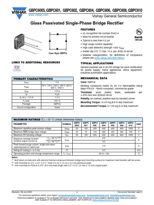
Glass Passivated Single-Phase Bridge RectifierLINKS TO ADDITIONAL RESOURCESFEATURES•UL recognition file number E54214•Ideal for printed circuit boards •Typical I R less than 0.5 μA •High surge current capability•High case dielectric strength 1500 V RMS•Solder dip 275 °C max. 10 s, per JESD 22-B106 •Material categorization: for definitions of compliance please see /doc?99912TYPICAL APPLICATIONSGeneral purpose use in AC/DC bridge full wave rectification for power supply, home appliances, office equipment, industrial automation applications.MECHANICAL DATACase: GBPC6Molding compound meets UL 94 V-0 flammability rating Base P/N-E4 - RoHS-compliant, commercial grade Terminals: silver plated leads, solderable per J-STD-002 and JESD22-B102Polarity: as marked, positive lead by beveled corner Mounting Torque: 10 cm-kg (8.8 in-lbs) maximum Recommended Torque: 5.7 cm-kg (5 in-lbs) maximumNotes(1)Bolt down on heat-sink with silicone thermal compound between bridge and mounting surface for maximum heat transfer with #6 screw (2)Unit mounted on 5.5" x 6.0" x 0.11" thick (14 cm x 15 cm x 0.3 cm) aluminum plate(3)Unit mounted on PCB at 0.375" (9.5 mm) lead length with 0.5" x 0.5" (12 mm x 12 mm) copper padsPRIMARY CHARACTERISTICSI F(AV) 6 AV RRM 50 V, 100 V, 200 V, 400 V, 600 V,800 V, 1000 VI FSM 175 A I R5 μA V F at I F = 3.0 A1.0 V T J max.150 °C Package GBPC6Circuit configurationQuadCase Style GBPC6~~3D 3D3D Model sMAXIMUM RATINGS (T A = 25 °C unless otherwise noted)PARAMETERSYMBOL GBPC 6005GBPC 601GBPC 602GBPC 604GBPC 606GBPC 608GBPC 610UNIT Maximum repetitive peak reverse voltage V RRM 501002004006008001000V Maximum RMS bridge input voltage V RMS 3570140280420560700V Maximum DC blocking voltage V DC 501002004006008001000V Maximum average forward rectified output current atT C = 50 °C (1)(2)I F(AV) 6.0A T A = 40 °C (3)3.0Peak forward surge current single sine-wave superimposed on rated load I FSM 175A Rating for fusing (t = 8.3 ms)I 2t 127A 2s Operating junction and storage temperature rangeT J , T STG-55 to +150°CNotes(1) Bolt down on heat-sink with silicone thermal compound between bridge and mounting surface for maximum heat transfer with #6 screw (2)Unit mounted on 5.5" x 6.0" x 0.11" thick (14 cm x 15 cm x 0.3 cm) aluminum plate(3)Unit mounted on PCB at 0.375" (9.5 mm) lead length with 0.5" x 0.5" (12 mm x 12 mm) copper padsRATINGS AND CHARACTERISTICS CURVES (T A = 25 °C unless otherwise noted)Fig. 1 - Derating Curve Output Rectified CurrentFig. 2 - Maximum Non-Repetitive Peak Forward Surge CurrentPer DiodeELECTRICAL CHARACTERISTICS (T A = 25 °C unless otherwise noted)PARAMETERSYMBOLTEST CONDITIONSGBPC 6005GBPC 601GBPC 602GBPC 604GBPC 606GBPC 608GBPC 610UNIT Maximum instantaneous forward voltage drop per diodeV F 3.0 A 1.0VMaximum DC reverse current at rated DC blocking voltage per diodeI R T A = 25 °C 5.0μA T A = 125 °C 500Typical junction capacitance per diodeC J4.0 V, 1 MHz18690pFTHERMAL CHARACTERISTICS (T A = 25 °C unless otherwise noted)PARAMETERSYMBOL GBPC6005GBPC 601GBPC 602GBPC 604GBPC 606GBPC 608GBPC 610UNIT Typical thermal resistance (1)R θJA 22°C/WR θJC7.3ORDERING INFORMATION (Example)PREFERRED P/N UNIT WEIGHT (g)PACKAGE CODEBASE QUANTITYDELIVERY MODEGBPC606-E4/513.251100Paper box5010015002.04.06.08.0Temperat u re (°C)1101005075100125150175200Nu m b er of Cycles at 60 HzP e a k F o r w a r d S u r g e C u r r e n t (A )Fig. 3 - Typical Forward Characteristics Per Diode Fig. 4 - Typical Reverse Leakage Characteristics Per Diode Fig. 5 - Typical Junction Capacitance Per DiodeFig. 6 - Typical Transient Thermal Impedance Per DiodePACKAGE OUTLINE DIMENSIONS in inches (millimeters)100.41.01.80.010.111000.60.81.21.61.4Instantaneo u s For w ard Voltage (V)I n s t a n t a n e o u s F o r w a r d C u r r e n t (A )204060801000.1110100Percent of Rated Peak Re v erse Voltage (%)I n s t a n t a n e o u s R e v e r s e C u r r e n t (µA )10000.1110100101001000Re v erse Voltage (V)J u n c t i o n C a p a c i t a n c e (p F )0.010.1 1 10 1000.1 110100t - Heating Time (s)T r a n s i e n t T h e r m a l I m p e d a n c e (°C /W )Case Style GBPC6Polarity sho w n on side of case: Positi v e lead b y b e v eled cornerMI N .0.048 (1.22)Legal Disclaimer Notice VishayDisclaimerALL PRODUCT, PRODUCT SPECIFICATIONS AND DATA ARE SUBJECT TO CHANGE WITHOUT NOTICE TO IMPROV E RELIABILITY, FUNCTION OR DESIGN OR OTHERWISE.V ishay Intertechnology, Inc., its affiliates, agents, and employees, and all persons acting on its or their behalf (collectively,“Vishay”), disclaim any and all liability for any errors, inaccuracies or incompleteness contained in any datasheet or in any other disclosure relating to any product.Vishay makes no warranty, representation or guarantee regarding the suitability of the products for any particular purpose or the continuing production of any product. To the maximum extent permitted by applicable law, Vishay disclaims (i) any and all liability arising out of the application or use of any product, (ii) any and all liability, including without limitation special, consequential or incidental damages, and (iii) any and all implied warranties, including warranties of fitness for particular purpose, non-infringement and merchantability.Statements regarding the suitability of products for certain types of applications are based on Vishay's knowledge of typical requirements that are often placed on Vishay products in generic applications. Such statements are not binding statements about the suitability of products for a particular application. It is the customer's responsibility to validate that a particular product with the properties described in the product specification is suitable for use in a particular application. Parameters provided in datasheets and / or specifications may vary in different applications and performance may vary over time. All operating parameters, including typical parameters, must be validated for each customer application by the customer's technical experts. Product specifications do not expand or otherwise modify Vishay's terms and conditions of purchase, including but not limited to the warranty expressed therein.Hyperlinks included in this datasheet may direct users to third-party websites. These links are provided as a convenience and for informational purposes only. Inclusion of these hyperlinks does not constitute an endorsement or an approval by Vishay of any of the products, services or opinions of the corporation, organization or individual associated with the third-party website. Vishay disclaims any and all liability and bears no responsibility for the accuracy, legality or content of the third-party website or for that of subsequent links.Except as expressly indicated in writing, Vishay products are not designed for use in medical, life-saving, or life-sustaining applications or for any other application in which the failure of the Vishay product could result in personal injury or death. Customers using or selling Vishay products not expressly indicated for use in such applications do so at their own risk. Please contact authorized Vishay personnel to obtain written terms and conditions regarding products designed for such applications. No license, express or implied, by estoppel or otherwise, to any intellectual property rights is granted by this document or by any conduct of Vishay. Product names and markings noted herein may be trademarks of their respective owners.© 2022 VISHAY INTERTECHNOLOGY, INC. ALL RIGHTS RESERVED。
BSM100GB60DLC中文资料
NutzungsbedingungenDie in diesem Produktdatenblatt enthaltenen Daten sind ausschließlich für technisch geschultes Fachpersonal bestimmt. Die Beurteilung der Geeignetheit dieses Produktes für die von Ihnen anvisierte Anwendung sowie die Beurteilung der Vollständigkeit der bereitgestellten Produktdaten für diese Anwendung obliegt Ihnen bzw. Ihren technischen Abteilungen.In diesem Produktdatenblatt werden diejenigen Merkmale beschrieben, für die wir eine liefervertragliche Gewährleistungübernehmen. Eine solche Gewährleistung richtet sich ausschließlich nach Maßgabe der im jeweiligen Liefervertrag enthaltenen Bestimmungen. Garantien jeglicher Art werden für das Produkt und dessen Eigenschaften keinesfalls übernommen.Sollten Sie von uns Produktinformationen benötigen, die über den Inhalt dieses Produktdatenblatts hinausgehen und insbesondere eine spezifische Verwendung und den Einsatz dieses Produktes betreffen, setzen Sie sich bitte mit dem für Siezuständigen Vertriebsbüro in Verbindung (siehe , Vertrieb&Kontakt). Für Interessenten halten wir ApplicationNotes bereit.Aufgrund der technischen Anforderungen könnte unser Produkt gesundheitsgefährdende Substanzen enthalten. Bei Rückfragenzu den in diesem Produkt jeweils enthaltenen Substanzen setzen Sie sich bitte ebenfalls mit dem für Sie zuständigen Vertriebsbüro in Verbindung.Sollten Sie beabsichtigen, das Produkt in gesundheits- oder lebensgefährdenden oder lebenserhaltenden Anwendungsbereichen einzusetzen, bitten wir um Mitteilung. Wir weisen darauf hin, dass wir für diese Fälle- die gemeinsame Durchführung eines Risiko- und Qualitätsassessments;- den Abschluss von speziellen Qualitätssicherungsvereinbarungen;- die gemeinsame Einführung von Maßnahmen zu einer laufenden Produktbeobachtung dringend empfehlen und gegebenenfalls die Belieferung von der Umsetzung solcher Maßnahmen abhängig machen.Soweit erforderlich, bitten wir Sie, entsprechende Hinweise an Ihre Kunden zu geben.Inhaltliche Änderungen dieses Produktdatenblatts bleiben vorbehalten.Terms & Conditions of usageThe data contained in this product data sheet is exclusively intended for technically trained staff. You and your technical departments will have to evaluate the suitability of the product for the intended application and the completeness of the productdata with respect to such application.This product data sheet is describing the characteristics of this product for which a warranty is granted. Any such warranty is granted exclusively pursuant the terms and conditions of the supply agreement. There will be no guarantee of any kind for the product and its characteristics.Should you require product information in excess of the data given in this product data sheet or which concerns the specific application of our product, please contact the sales office, which is responsible for you (see , sales&contact). For those that are specifically interested we may provide application notes.Due to technical requirements our product may contain dangerous substances. For information on the types in question please contact the sales office, which is responsible for you.Should you intend to use the Product in health or live endangering or life support applications, please notify. Please note, that for any such applications we urgently recommend- to perform joint Risk and Quality Assessments;- the conclusion of Quality Agreements;- to establish joint measures of an ongoing product survey,and that we may make delivery depended on the realizationof any such measures.If and to the extent necessary, please forward equivalent notices to your customers.Changes of this product data sheet are reserved.。
CS5460A中文数据手册

单相双向功率/电能 IC
特性
l l l l l l l l l l l l l l l 电能数据线性度:在1000 :1 动态范围内线性度 为 ±0.1% 片内功能:可以测量电能(有功),I *V,IRMS 和 VRMS ,具有电能-脉冲转换功能 可以从串行EEPROM 智能“自引导”,不需要微 控制器 AC 或DC 系统校准 具有机械计度器/步进电机驱动器 符合IEC687/1036 ,JIS 工业标准 功耗<12mW 优化的分流器接口 V对I的相位补偿 单电源地参考信号 片内2.5V 参考电压(最大温漂60ppm/℃) 简单的三线数字串行接口 看门狗定时器 内带电源监视器 电源配置 VA+ = +5 V; VA- = 0V; VD+ = +3.3V~+5 V
概述
CS5460A 是一个包含两个ΔΣ模 - 数转换 器(ADC)、高速电能计算功能和一个串行接 口的高度集成的ΔΣ 模-数转换器。 它可以精确 测量和计算有功电能、 瞬时功率、 IRMS 和VRMS , 用于研制开发单相2 线或3 线电表。CS5460A 可以使用低成本的分流器或互感器测量电流, 使 用分压电阻或电压互感器测量电压。CS5460A 具有与微控制器通讯的双向串口, 芯片的脉冲输 出频率与有功能量成正比。CS5460A 具有方便 的片上AC/DC 系统校准功能。 “自引导”的特点使 CS5460A 能独自工 作, 在系统上电后自动初始化。 在自引导模式中, CS5460A 从一个外部EEPROM 中读取校准数 据和启动指令。使用该模式时,CS5460A 工作 时不需要外加微控制器, 因此当电表用于大批量 住宅电能测量时,可降低电表的成本。 订货信息: CS5460A-BS -40℃~+85℃ 24 引脚 SSOP
GB160160BNGBBMUB-V00中文资料

JEWEL HILL ELECTRONIC CO.,LTDJEWEL HILL ELECTRONIC CO.,LTD.SPECIFICATIONS FORLCD MODULEModule No. GB160160BOffice Address: Rm. 518,5/F., 101 Shangbu Industrial District,HuaqiangNorthRoad, Shenzhen, ChinaTEL : (86)-755-83362489 83617492FAX: (86)-755-83286396 83365871E-mail: sales@jhlcd@Website: TABLE OF CONTENTSLCM NUMBER SYSTEM (2)1. GENERAL DESCRIPTION (3)2. FEATURES (3)3. MECHANICAL SPECIFICATION (3)4. MECHANICAL DIMENSION (4)5. MAXIMUM RATINGS (5)6. ELECTRICAL CHARACTERISTICS (5)7. MODULE FUNCTION DESCRIPTION (6)8. ELECTRO-OPTICAL CHARACTERISTICS (13)9. RELIABILITY (17)10. PRECAUTIONS FOR USING LCD MODULES (18)11. USING LCD MODULES (20)12. REVISION HISTORY (22)SAMPLE APPROVED REPORT (23)LCM Number SystemNUMBER OF CHAR. PER LINE F: FSTN; X: OTHER VERSION NUMBER: V00~V99IC TYPE:VIEWING DIRECTION:TEMPERATURE RANGE:BACKLIGHT TYPE:SERIAL NUMBER: A~ZGRAPHIC MODULEs: NUMBER OF COMMONs GRAPHIC MODULEs:NUMBER OF SEGMENTs COB & SMT LCM BACKLIGHT COLOR:CHARACTER MODULEs:CHARACTER MODULEs: NUMBER OF LINE G: REFLECTIVE,NONE BACKLIGHT A: TRANSFLECTIVE, EL BACKLIGHT B: TRANSMISSIVE, EL BACKLIGHT C: TRANSFLECTIVE, LED BACKLIGHT D: TRANSMISSIVE, LED BACKLIGHT E: TRANSFLECTIVE, CCFL BACKLIGHT F: TRANSMISSIVE, CCFL BACKLIGHT A: AMBER; B: BLUE; Y: YELLOW-GREEN R: RED; W: WHITE; O: THER COLOR N: NORMAL TEMPERATURE RANGE U: UPPER(12:00); D: DOWN(6:00)L: LEFT(9:00); R: RIGHT(3:00);A: BONDING IC, WITH CONTROLLER B: BONDING IC, WITHOUT CONTROLLER C: SMT IC, WITH CONTROLLER D: SMT IC, WITHOUT CONTROLLER O: OTHER TYPEW: BLACK-WHITE; O: OTHER G: GRAY; Y: YELLOW-GREEN; B: BLUE; LCD COLOR MODE:N: TN; H: HTN; S: STN LCD TYPE:S: SUPER WIDE TEMPERATURE RANGE W: WIDE TEMPERATURE RANGEM: MIDDLE TEMPERATURE RANGE1. GENERAL DESCRIPTIONThe GB160160B is a 160 x 160 Dots Graphics LCD module. It has a STN panel composed of160segments and 160 commons. The LCM can be easily accessed by micro-controller via parallel interface.2. FEATURESTransflective and PositiveDisplay ModeSTN(Y-G) moduleDisplay Format Graphic 160 x 160 dotsInput Data Parallel data input from MCUMultiplexing Ratio 1/160 DutyBiasBias 1/12Viewing Direction 6 O’clock(Yellow-Green)Backlight LED3. MECHANICAL SPECIFICATIONItem Specifications Unit Dimensional outline 89.2 x 85.0 x 14.6(max) mmResolution 160segs x 160coms dotsActive area 60.775(W) x 60.775(H) mmDots pitch 0.38(W)×0.38(H) mmDots size 0.355(W)×0.355 (H) mm4. MECHANICAL DIMENSION5. MAXIMUM RATINGSItem Symbol Min Max Unit NoteV DD - V ss -0.3 5.5 V Supply voltage V LCD -0.3 24.0 V Input Voltage V IN -0.3 V DD +0.3 VOperating temperature T OPR 0 +50 Storage temperature T STR -10 +60Humidity --- --- 90 %RH6. ELECTRICAL CHARACTERISTICSItem SymbolCondition Min. Typ. Max. UnitSupply Voltage Logic V DD ------ 5.0 --- VH level V IH 0.8V DD --- V DDInput VoltageL levelV IL --- V SS --- 0.2V DDVCurrent Consumption(LCD DRIVER)I DD V DD =5.0V; V LCD =19.0V, T amb =25 ;--- --- 1.5 mALCD Driving Voltage V LCDBias=1/13V LCD =V DD -V 518.7 19.0 19.3 VCurrent Consumption (With LED BackLight)I LEDV DD =5.0V;V LED =4.2V,T amb =25 ;--- --- TBD mA7. MODULE FUNCTION DESCRIPTION7.1. PIN DESCRIPTIONINTERFACE WITH CN1 & CN2:PinSymbol Description No.1 VSSPower supply for Ground (0V)2 MAC Signal for LCD Driver Output3 FLMData Input for Common ICs4 CL1Data Latch Colok5 CL2Data Shift Colok6 D37 D2Display Data Input Terminal for Segment ICs8 D19 D010 VEE Power Supply for Negative V oltage11 VDD Power supply for positive (+5V)12 V0 VLCD V oltage Regulation Terminal13 /DISPOFF Display OFF Control14 K Power Supply for LED BackLight Negative15 A Power Supply for LED BackLight Positive7.2 TIMING CHARACTERISTICS7.3 APPLICATION OF LCMLED-LED+VDD VSS VEE V0D0-D4CL1CL2M FLMCircuit Block Diagram8. ELECTRO-OPTICAL CHARACTERISTICSItem Symbol Condition Temp Min Typ. Max UnitsNote--- 19.5 ---25 18.7 19.0 19.3 LCD driving voltageV LCD = = 050 --- 18.0 --- V NOTE1Rise Time (Tr) --- --- -- Decay Time (Tf)0 --- ---- --- Rise Time (Tr) --- 225 340Decay Time (Tf) 25 --- 240 360Rise Time (Tr) --- --- -- Response TimeDecay Time (Tf)= = 0 50 --- --- --msec NOTE2Contrast Ratio Cr= = 0 255 10 --- --- NOTE4Viewing AngleRange( = 0°)(6”) = 90°(3”) =180°(12”) =270°(9”)(25 ) CR ≥245 35 25 35DegNOTE3z For panel only․Electro-Optical Characteristics Measuring Equipment(DMS501)SystemIllumination (D65)․Note 1. Definition of Driving Voltage( Vlcd) :․Note 3. Definition of Viewing Angle and :․Note 4. Definition of Contrast ratio( CR) :Brightness of Non-selected Segment (B2)Brightness of Selected Segment (B1)CR =V,maxCR,maxDriving VoltageB r i gh t n e s s (%)Brightness Curve forSelected Segment0%=90 =270Viewing Direction 6 O’clock DirectionNormal :9. RELIABILITY9.1. MTBFThe LCD module shall be designed to meet a minimum MTBF value of 50000 hours with normal. (25°C in the room without sunlight)9.2. TESTSNO. ITEM CONDITION CRITERION 1 High Temperature Operating 50 120Hrs2 Low Temperature Operating 0 120Hrs3 High Temperature/Humidity Non-Operating50 ,90%RH ,120 Hrs4 High TemperatureNon-Operating60 120Hrs5 Low TemperatureNon-Operating-10 120Hrs6 Temperature CyclingNon-Operating 0 (30Min )↔ 50 (30Min)10 CYCLESNo Defect OfOperational Function InRoom Temperature AreAllowable.IDD of LCM inPre-and post-test shouldfollow specificationNotes: Judgments should be mode after exposure in room temperature for two hours.10. PRECAUTIONS FOR USING LCD MODULES10.1. HANDLING PRECAUTIONS(1) The display panel is made of glass. Do not subject it to a mechanical shock or impact by droppingit.(2) If the display panel is damaged and the liquid crystal substance leaks out, be sure not to get any inyour mouth. If the substance contacts your skin or clothes, wash it off using soap and water.(3) Do not apply excessive force to the display surface or the adjoining areas since this may cause thecolor tone to vary.(4) The polarizer covering the display surface of the LCD module is soft and easily scratched. Handlethis polarizer carefully.(5) If the display surface becomes contaminated, breathe on the surface and gently wipe it with a softdry cloth. If it is heavily contaminated, moisten a cloth with one of the following solvents: - Isopropyl alcohol- Ethyl alcohol(6) Solvents other than those above mentioned may damage the polarizer.Especially, do not use the following:- Water- Ketone- Aromatic solvents(7) Extra care to minimize corrosion of the electrode. Water droplets, moisture condensation or acurrent flow in a high-humidity environment accelerates corrosion of the electrode.(8) Install the LCD Module by using the mounting holes. When mounting the LCD Module, makesure it is free of twisting, warping and distortion. In particular, do not forcibly pull or bend the I/Ocable or the backlight cable.(9) Do not attempt to disassemble or process the LCD Module.(10) NC terminal should be open. Do not connect anything.(11) If the logic circuit power is off, do not apply the input signals.(12) To prevent destruction of the elements by static electricity, be careful to maintain an optimumwork environment.- Be sure to ground the body when handling he LCD Module.- Tools required for assembling, such as soldering irons, must be properly grounded.-To reduce the amount of static electricity generated, do not conduct assembling and other workunder dry conditions.-The LCD Module is coated with a film to protect the display surface. Exercise care when peeling off this protective film since static electricity may be generated.10.2. STORAGE CONDITIONSWhen storing, avoid the LCD module to be exposed to direct sunlight of fluorescent lamps. For stability, to keep it away form high temperature and high humidity environment (The best condition is : 23±5°C, 45±20%RH). ESD protection is necessary for long-term storage also.10.3. OTHERSLiquid crystals solidify under low temperature (below the storage temperature range) leading to defective orientation or the generation of air bubbles (black or white). Air bubbles may also be generated if the module is subject to a low temperature.If the LCD Module have been operating for a long time showing the same display patterns the display patterns may remain on the screen as ghost images and a slight contrast irregularity may also appear.A normal operating status can be recovered by suspending use for some time. It should be noted that this phenomenon does not adversely affect performance reliability.To minimize the performance degradation of the LCD Module resulting from destruction caused by static electricity etc. exercise care to avoid holding the following sections when handling the modules.- Exposed area of the printed circuit board.- Terminal electrode sections.11. Using LCD modules11.1 LIQUID CRYSTAL DISPLAY MODULESLCD is composed of glass and polarizer. Pay attention to the following items when handling.(1) Please keep the temperature within specified range for use and storage. Polarization degradation,bubble generation or polarizer peel-off may occur with high temperature and high humidity.(2) Do not touch, push or rub the exposed polarizers with anything harder than a HB pencil lead (glass,tweezers, etc).(3) N-hexane is recommended for cleaning the adhesives used to attach front/rear polarizers andreflectors made of organic substances, which will be damaged by chemicals such as acetone, toluene, toluene, ethanol and isopropyl alcohol.(4) When the display surface becomes dusty, wipe gently with absorbent cotton or other soft materiallike chamois soaked in petroleum ether. Do not scrub hard to avoid damaging the display surface.(5) Wipe off saliva or water drops immediately, contact with water over a long period of time maycause deformation or color fading.(6) Avoid contacting oil and fats.(7) Condensation on the surface and contact with terminals due to cold will damage, stain orpolarizers. After products are tested at low temperature they must be warmed up in a container before coming is contacting with room temperature air.(8) Do not put or attach anything on the display area to avoid leaving marks on.(9) Do not touch the display with bare hands. This will stain the display area and degrade insulationbetween terminals (some cosmetics are determinate to the polarizers).(10)As glass is fragile, it tends to become or chipped during handling especially on the edges. Pleaseavoid dropping or jarring.11.2 INSTALLING LCD MODULEAttend to the following items when installing the LCM.(1) Cover the surface with a transparent protective plate to protect the polarizer and LC cell.(2) When assembling the LCM into other equipment, the spacer to the bit between the LCM and thefitting plate should have enough height to avoid causing stress to the module surface, refer to the individual specifications for measurements. The measurement tolerance should be ±0.1mm.11.3 ELECTRO-STATIC DISCHARGE CONTROLSince this module uses a CMOS LSI, the same careful attention should be paid for electrostatic discharge as for an ordinary CMOS IC.(1) Make certain that you are grounded when handing LCM.(2) Before removing LCM from its packing case or incorporating it into a set, be sure the module andyour body have the same electric potential.(3) When soldering the terminal of LCM, make certain the AC power source for the soldering irondoes not leak.(4) When using an electric screwdriver to attach LCM, the screwdriver should be of groundpotentiality to minimize as much as possible any transmission of electromagnetic waves produced sparks coming from the commutator of the motor.(5) As far as possible, make the electric potential of your work clothes and that of the workbenches tothe ground potential.(6) To reduce the generation of electro-static discharge, be careful that the air in the work is not toodried. A relative humidity of 50%-60% is recommended.11.4 PRECAUTIONS FOR OPERATION(1) Viewing angle varies with the change of liquid crystal driving voltage (Vo). Adjust Vo to showthe best contrast.(2) Driving the LCD in the voltage above the limit will shorten its lifetime.(3) Response time is greatly delayed at temperature below the operating temperature range. However,this does not mean the LCD will be out of the order. It will recover when it returns to the specified temperature range.(4) If the display area is pushed hard during operation, the display will become abnormal. However, itwill return to normal if it is turned off and then on.(5) Condensation on terminals can cause an electrochemical reaction disrupting the terminal circuit.Therefore, this product must be used and stored within the specified condition of 23±5°C, 45±20%RH.(6) When turning the power on, input each signal after the positive/negative voltage becomes stable.11.5 SAFETY(1) It is recommended to crush damaged or unnecessary LCDs into pieces and wash them off withsolvents such as acetone and ethanol, which should later be burned.(2) If any liquid leaks out of a damaged glass cell and comes in contact with the hands, wash offthoroughly with soap and water.12. REVISION HISTORYrecord Date Version Reviseversion 06-05-241.0 Original2.0 Change contact mode 06-08-04SAMPLE APPROVED REPORT。
型号GA-60

型号GA-60可便携式电化学式及红外光传感器烟气分析仪烟气分析仪GA-60采用最新进技术设计,模块版设计结构可使仪器内部更加紧致,并使维修更具人性化。
GA-60装配二组微处理器,可使其有条不紊处理各种挑战。
深信我们的GA-60已使用各种可预测的设计智能。
仪器各部份组件,是以长时间无故障操作之要求设计,标准版本装备五颗电化学传感器(氧分率、一氧化碳、一氧化氮、二氧化氮、二氧化硫),并可装置第六颗电化学传感器与二组用于量测二氧化碳与甲烷之红外光传感器。
特性:○量测结果图形显示:●变量显示可以不需要编辑●垂直轴刻度可手动或自动调整○内存:●可连续储存768笔资料,可切分至10组数据库。
○打印机:●量测结果如实时值或平均值●显示屏内容●平均值定时打印●仪器内部参数细节○量测方法:●平均时间可由使用者修改(10秒至60分钟)●显示可切换实时值及平均值画面○气体传感器技术:●藉由温度及交叉灵敏度之计算补偿取得线性化●绝对及相对质量浓度及相对排放值计算●氧分率传感器在使用时具有校正可许性○可编辑燃烧参数:●内建22种一般常用燃料种类之资料●可扩充10种燃料之资料○温度量测:●选择热偶计种类 (PtRh-Pt 或 Ni-CrNi)○黑度测试:●多种语言选择○服务及测试功能:●以声响及显示方式提供错误警讯●探头连结自动检查功能●密码保护仪器设定功能●开放式校正选单可显示交叉灵敏度技术指针:参数内容描述使用电化学式传感器可量测之气体种类O2, CO, NO, NO2, SO2, H2S, Cl2, H2等细节部分详参下列表格所列电化学式资料使用红外光传感器可量测之气体种类CO2, CH4等细节部分详参下列表格所列红外光式资料打印机热感式打印机,使用宽度80 mm热感纸。
显示屏图形-液晶显示屏,具背光,显示黑度可调整,240 x128 pixels。
数据存储器内存容量768笔数据,可切分10组数据库。
时钟实时时钟及日期输出入接口RS232C气体采样泵浦膜片式泵浦,流量电子控制。
E-VAC系列中压真空断路器

E-VAC 系列中压真空断路器伊顿电气的E-VAC 系列真空断路器融合了伊顿电气真空技术的卓越性能,集中体现了伊顿电气数十年配电系统方面丰富的设计和制造经验,具有可靠性高,操作方便,维护简单等特点,为中国用户提供了高性价比的产品。
符合IEC 、GB 、DL 等标准的规定 E-VAC 配用伊顿电气新一代的真空灭弧室,更适合电力系统的技术和运行条件 理想的触头材料和形状,保证小的截流值和稳定的接触电阻 零部件少,结构紧凑合理,确保操作更可靠、更安全 可理想的切合电阻、感性和容性负荷 在二次插头、底盘车、动触头以及接地方式等各方面的设计符合中国用户习惯,与国内主流中压开关柜KYN28柜型完全兼容产品使用条件周围空气温度不超过40℃,且在 24h 内测得的平均值不超过35℃。
最低周围空气温度为-15℃ 阳光辐射的影响可以忽略 周围空气没有明显的受到尘埃、烟、腐蚀性或可燃性气体、蒸汽或盐雾的污染 地震烈度不超过8度在二次系统中感应的电磁干扰的幅值不超过1.6kV技术特点E-VAC 采用成熟的弹簧操作机构,性能稳定、可靠,寿命长,操作简单,优秀的防腐蚀能力,寿命期内只需极少维护 E-VAC 采用了立式环氧绝缘筒可防御严酷环境的影响,使E-VAC 断路器适用于各种场合。
独特的触头材料和一次梅花触头应用,使E-VAC 断路器适用于中压系统的各种场合 按GB1984-2003中延长的电寿命E2级、延长的机械寿命M2级及容性电流开合具有非常低的重击穿概率C2级型式试验 外形尺寸和配柜联锁方式与国内主流中压开关柜KYN28柜完全兼容,通用性高,大大降低设计费用 产品装配采用工装保证尺寸的一致性,所有产品在出厂前均进行过标准柜的推柜试验,保证了产品的可互换性和通用性 所有产品出厂前经过数百次机械操作磨合试验,确保了产品性能处于最稳定的阶段 采用先进的进口测试设备,真实记录每一台产品的空载机械特性,并向用户提供这些特性曲线,确保产品质量的可靠性湿度条件应用领域在24h内测得的相对湿度平均值不超过95%在24h内测得的水蒸气压力平均值不超过2.2kPa月相对湿度平均值不超过90%月水蒸气压力平均值不超过1.8kPa主要规格与技术参数项目 化工工业石油工业管道工业海上开采造船工业造纸工业露天煤矿单位数值变电所,变电站水泥工业汽车工业发电厂纺织及食品工业冶金工业额定电压kV 12额定短时工频耐受电压(1 min)kV 42(相对地,相间) 48(断口)额定雷电冲击耐受电压(峰值)kV 75(相对地,相间) 85(断口)额定频率Hz 50额定电流 A 630 630 1250 1250 1600 1250 16001250 1600 2000 2000 2500 2000 25003150 4000(1) 3150 4000(1)额定短路开断电流kA 25 31.5 40 50额定短时耐受电流(4s)kA 25 31.5 40 50额定峰值耐受电流kA 63 80 100(2) 125额定短路关合电流kA63 80 100(2) 125机械寿命次20000, (50kA为10000次)额定电流开断次数次20000, (50kA为10000次)额定短路电流开断次数次E2(274)注:(1) 4000A需要强制风冷。
ATEX Certificate system, ATEX 防爆认证标准

Class I, Zone 0, AEx ia IIC T4
Means: Class I Zone 0 A Ex ia IIC T4 Flammable gas or vapor Area classification (explosive atmosphere present continuously) Conformity to US requirements Explosion protected Protection method (Intrinsic Safety) Gas group (acetylene & hydrogen) Temperature class
Zone/Division
Area Classification
Flammable Material Present Intermittently (10…1000 h/y) Zone 1 Flammable Material Present Abnormally (< 10 h/y) Zone 2
IIC/Groups
Hazardous Locations Groups
Typical Hazard Acetylene Hydrogen Ethylene Propane Methane Metal Dust Coal Dust Grain Dust Fibers North America CEC Section 18, NEC Article 500 Class I/Group A or IIC Class I/Group B or IIC Class I/Group C or IIB Class I/Group D or IIA Group D (gaseous mines) or I Class II/Group E Class II/Group F Class II/Group G Class III CENELEC/IEC CENELEC EN50014, IEC 60079 IIC IIC IIB IIA I — — — —
- 1、下载文档前请自行甄别文档内容的完整性,平台不提供额外的编辑、内容补充、找答案等附加服务。
- 2、"仅部分预览"的文档,不可在线预览部分如存在完整性等问题,可反馈申请退款(可完整预览的文档不适用该条件!)。
- 3、如文档侵犯您的权益,请联系客服反馈,我们会尽快为您处理(人工客服工作时间:9:00-18:30)。
JEWEL HILL ELECTRONIC CO.,LTDJEWEL HILL ELECTRONIC CO.,LTD.SPECIFICATIONS FORLCD MODULEModule No. GB160160BOffice Address: Rm. 518,5/F., 101 Shangbu Industrial District,HuaqiangNorthRoad, Shenzhen, ChinaTEL : (86)-755-83362489 83617492FAX: (86)-755-83286396 83365871E-mail: sales@jhlcd@Website: TABLE OF CONTENTSLCM NUMBER SYSTEM (2)1. GENERAL DESCRIPTION (3)2. FEATURES (3)3. MECHANICAL SPECIFICATION (3)4. MECHANICAL DIMENSION (4)5. MAXIMUM RATINGS (5)6. ELECTRICAL CHARACTERISTICS (5)7. MODULE FUNCTION DESCRIPTION (6)8. ELECTRO-OPTICAL CHARACTERISTICS (13)9. RELIABILITY (17)10. PRECAUTIONS FOR USING LCD MODULES (18)11. USING LCD MODULES (20)12. REVISION HISTORY (22)SAMPLE APPROVED REPORT (23)LCM Number SystemNUMBER OF CHAR. PER LINE F: FSTN; X: OTHER VERSION NUMBER: V00~V99IC TYPE:VIEWING DIRECTION:TEMPERATURE RANGE:BACKLIGHT TYPE:SERIAL NUMBER: A~ZGRAPHIC MODULEs: NUMBER OF COMMONs GRAPHIC MODULEs:NUMBER OF SEGMENTs COB & SMT LCM BACKLIGHT COLOR:CHARACTER MODULEs:CHARACTER MODULEs: NUMBER OF LINE G: REFLECTIVE,NONE BACKLIGHT A: TRANSFLECTIVE, EL BACKLIGHT B: TRANSMISSIVE, EL BACKLIGHT C: TRANSFLECTIVE, LED BACKLIGHT D: TRANSMISSIVE, LED BACKLIGHT E: TRANSFLECTIVE, CCFL BACKLIGHT F: TRANSMISSIVE, CCFL BACKLIGHT A: AMBER; B: BLUE; Y: YELLOW-GREEN R: RED; W: WHITE; O: THER COLOR N: NORMAL TEMPERATURE RANGE U: UPPER(12:00); D: DOWN(6:00)L: LEFT(9:00); R: RIGHT(3:00);A: BONDING IC, WITH CONTROLLER B: BONDING IC, WITHOUT CONTROLLER C: SMT IC, WITH CONTROLLER D: SMT IC, WITHOUT CONTROLLER O: OTHER TYPEW: BLACK-WHITE; O: OTHER G: GRAY; Y: YELLOW-GREEN; B: BLUE; LCD COLOR MODE:N: TN; H: HTN; S: STN LCD TYPE:S: SUPER WIDE TEMPERATURE RANGE W: WIDE TEMPERATURE RANGEM: MIDDLE TEMPERATURE RANGE1. GENERAL DESCRIPTIONThe GB160160B is a 160 x 160 Dots Graphics LCD module. It has a STN panel composed of160segments and 160 commons. The LCM can be easily accessed by micro-controller via parallel interface.2. FEATURESTransflective and PositiveDisplay ModeSTN(Y-G) moduleDisplay Format Graphic 160 x 160 dotsInput Data Parallel data input from MCUMultiplexing Ratio 1/160 DutyBiasBias 1/12Viewing Direction 6 O’clock(Yellow-Green)Backlight LED3. MECHANICAL SPECIFICATIONItem Specifications Unit Dimensional outline 89.2 x 85.0 x 14.6(max) mmResolution 160segs x 160coms dotsActive area 60.775(W) x 60.775(H) mmDots pitch 0.38(W)×0.38(H) mmDots size 0.355(W)×0.355 (H) mm4. MECHANICAL DIMENSION5. MAXIMUM RATINGSItem Symbol Min Max Unit NoteV DD - V ss -0.3 5.5 V Supply voltage V LCD -0.3 24.0 V Input Voltage V IN -0.3 V DD +0.3 VOperating temperature T OPR 0 +50 Storage temperature T STR -10 +60Humidity --- --- 90 %RH6. ELECTRICAL CHARACTERISTICSItem SymbolCondition Min. Typ. Max. UnitSupply Voltage Logic V DD ------ 5.0 --- VH level V IH 0.8V DD --- V DDInput VoltageL levelV IL --- V SS --- 0.2V DDVCurrent Consumption(LCD DRIVER)I DD V DD =5.0V; V LCD =19.0V, T amb =25 ;--- --- 1.5 mALCD Driving Voltage V LCDBias=1/13V LCD =V DD -V 518.7 19.0 19.3 VCurrent Consumption (With LED BackLight)I LEDV DD =5.0V;V LED =4.2V,T amb =25 ;--- --- TBD mA7. MODULE FUNCTION DESCRIPTION7.1. PIN DESCRIPTIONINTERFACE WITH CN1 & CN2:PinSymbol Description No.1 VSSPower supply for Ground (0V)2 MAC Signal for LCD Driver Output3 FLMData Input for Common ICs4 CL1Data Latch Colok5 CL2Data Shift Colok6 D37 D2Display Data Input Terminal for Segment ICs8 D19 D010 VEE Power Supply for Negative V oltage11 VDD Power supply for positive (+5V)12 V0 VLCD V oltage Regulation Terminal13 /DISPOFF Display OFF Control14 K Power Supply for LED BackLight Negative15 A Power Supply for LED BackLight Positive7.2 TIMING CHARACTERISTICS7.3 APPLICATION OF LCMLED-LED+VDD VSS VEE V0D0-D4CL1CL2M FLMCircuit Block Diagram8. ELECTRO-OPTICAL CHARACTERISTICSItem Symbol Condition Temp Min Typ. Max UnitsNote--- 19.5 ---25 18.7 19.0 19.3 LCD driving voltageV LCD = = 050 --- 18.0 --- V NOTE1Rise Time (Tr) --- --- -- Decay Time (Tf)0 --- ---- --- Rise Time (Tr) --- 225 340Decay Time (Tf) 25 --- 240 360Rise Time (Tr) --- --- -- Response TimeDecay Time (Tf)= = 0 50 --- --- --msec NOTE2Contrast Ratio Cr= = 0 255 10 --- --- NOTE4Viewing AngleRange( = 0°)(6”) = 90°(3”) =180°(12”) =270°(9”)(25 ) CR ≥245 35 25 35DegNOTE3z For panel only․Electro-Optical Characteristics Measuring Equipment(DMS501)SystemIllumination (D65)․Note 1. Definition of Driving Voltage( Vlcd) :․Note 3. Definition of Viewing Angle and :․Note 4. Definition of Contrast ratio( CR) :Brightness of Non-selected Segment (B2)Brightness of Selected Segment (B1)CR =V,maxCR,maxDriving VoltageB r i gh t n e s s (%)Brightness Curve forSelected Segment0%=90 =270Viewing Direction 6 O’clock DirectionNormal :9. RELIABILITY9.1. MTBFThe LCD module shall be designed to meet a minimum MTBF value of 50000 hours with normal. (25°C in the room without sunlight)9.2. TESTSNO. ITEM CONDITION CRITERION 1 High Temperature Operating 50 120Hrs2 Low Temperature Operating 0 120Hrs3 High Temperature/Humidity Non-Operating50 ,90%RH ,120 Hrs4 High TemperatureNon-Operating60 120Hrs5 Low TemperatureNon-Operating-10 120Hrs6 Temperature CyclingNon-Operating 0 (30Min )↔ 50 (30Min)10 CYCLESNo Defect OfOperational Function InRoom Temperature AreAllowable.IDD of LCM inPre-and post-test shouldfollow specificationNotes: Judgments should be mode after exposure in room temperature for two hours.10. PRECAUTIONS FOR USING LCD MODULES10.1. HANDLING PRECAUTIONS(1) The display panel is made of glass. Do not subject it to a mechanical shock or impact by droppingit.(2) If the display panel is damaged and the liquid crystal substance leaks out, be sure not to get any inyour mouth. If the substance contacts your skin or clothes, wash it off using soap and water.(3) Do not apply excessive force to the display surface or the adjoining areas since this may cause thecolor tone to vary.(4) The polarizer covering the display surface of the LCD module is soft and easily scratched. Handlethis polarizer carefully.(5) If the display surface becomes contaminated, breathe on the surface and gently wipe it with a softdry cloth. If it is heavily contaminated, moisten a cloth with one of the following solvents: - Isopropyl alcohol- Ethyl alcohol(6) Solvents other than those above mentioned may damage the polarizer.Especially, do not use the following:- Water- Ketone- Aromatic solvents(7) Extra care to minimize corrosion of the electrode. Water droplets, moisture condensation or acurrent flow in a high-humidity environment accelerates corrosion of the electrode.(8) Install the LCD Module by using the mounting holes. When mounting the LCD Module, makesure it is free of twisting, warping and distortion. In particular, do not forcibly pull or bend the I/Ocable or the backlight cable.(9) Do not attempt to disassemble or process the LCD Module.(10) NC terminal should be open. Do not connect anything.(11) If the logic circuit power is off, do not apply the input signals.(12) To prevent destruction of the elements by static electricity, be careful to maintain an optimumwork environment.- Be sure to ground the body when handling he LCD Module.- Tools required for assembling, such as soldering irons, must be properly grounded.-To reduce the amount of static electricity generated, do not conduct assembling and other workunder dry conditions.-The LCD Module is coated with a film to protect the display surface. Exercise care when peeling off this protective film since static electricity may be generated.10.2. STORAGE CONDITIONSWhen storing, avoid the LCD module to be exposed to direct sunlight of fluorescent lamps. For stability, to keep it away form high temperature and high humidity environment (The best condition is : 23±5°C, 45±20%RH). ESD protection is necessary for long-term storage also.10.3. OTHERSLiquid crystals solidify under low temperature (below the storage temperature range) leading to defective orientation or the generation of air bubbles (black or white). Air bubbles may also be generated if the module is subject to a low temperature.If the LCD Module have been operating for a long time showing the same display patterns the display patterns may remain on the screen as ghost images and a slight contrast irregularity may also appear.A normal operating status can be recovered by suspending use for some time. It should be noted that this phenomenon does not adversely affect performance reliability.To minimize the performance degradation of the LCD Module resulting from destruction caused by static electricity etc. exercise care to avoid holding the following sections when handling the modules.- Exposed area of the printed circuit board.- Terminal electrode sections.11. Using LCD modules11.1 LIQUID CRYSTAL DISPLAY MODULESLCD is composed of glass and polarizer. Pay attention to the following items when handling.(1) Please keep the temperature within specified range for use and storage. Polarization degradation,bubble generation or polarizer peel-off may occur with high temperature and high humidity.(2) Do not touch, push or rub the exposed polarizers with anything harder than a HB pencil lead (glass,tweezers, etc).(3) N-hexane is recommended for cleaning the adhesives used to attach front/rear polarizers andreflectors made of organic substances, which will be damaged by chemicals such as acetone, toluene, toluene, ethanol and isopropyl alcohol.(4) When the display surface becomes dusty, wipe gently with absorbent cotton or other soft materiallike chamois soaked in petroleum ether. Do not scrub hard to avoid damaging the display surface.(5) Wipe off saliva or water drops immediately, contact with water over a long period of time maycause deformation or color fading.(6) Avoid contacting oil and fats.(7) Condensation on the surface and contact with terminals due to cold will damage, stain orpolarizers. After products are tested at low temperature they must be warmed up in a container before coming is contacting with room temperature air.(8) Do not put or attach anything on the display area to avoid leaving marks on.(9) Do not touch the display with bare hands. This will stain the display area and degrade insulationbetween terminals (some cosmetics are determinate to the polarizers).(10)As glass is fragile, it tends to become or chipped during handling especially on the edges. Pleaseavoid dropping or jarring.11.2 INSTALLING LCD MODULEAttend to the following items when installing the LCM.(1) Cover the surface with a transparent protective plate to protect the polarizer and LC cell.(2) When assembling the LCM into other equipment, the spacer to the bit between the LCM and thefitting plate should have enough height to avoid causing stress to the module surface, refer to the individual specifications for measurements. The measurement tolerance should be ±0.1mm.11.3 ELECTRO-STATIC DISCHARGE CONTROLSince this module uses a CMOS LSI, the same careful attention should be paid for electrostatic discharge as for an ordinary CMOS IC.(1) Make certain that you are grounded when handing LCM.(2) Before removing LCM from its packing case or incorporating it into a set, be sure the module andyour body have the same electric potential.(3) When soldering the terminal of LCM, make certain the AC power source for the soldering irondoes not leak.(4) When using an electric screwdriver to attach LCM, the screwdriver should be of groundpotentiality to minimize as much as possible any transmission of electromagnetic waves produced sparks coming from the commutator of the motor.(5) As far as possible, make the electric potential of your work clothes and that of the workbenches tothe ground potential.(6) To reduce the generation of electro-static discharge, be careful that the air in the work is not toodried. A relative humidity of 50%-60% is recommended.11.4 PRECAUTIONS FOR OPERATION(1) Viewing angle varies with the change of liquid crystal driving voltage (Vo). Adjust Vo to showthe best contrast.(2) Driving the LCD in the voltage above the limit will shorten its lifetime.(3) Response time is greatly delayed at temperature below the operating temperature range. However,this does not mean the LCD will be out of the order. It will recover when it returns to the specified temperature range.(4) If the display area is pushed hard during operation, the display will become abnormal. However, itwill return to normal if it is turned off and then on.(5) Condensation on terminals can cause an electrochemical reaction disrupting the terminal circuit.Therefore, this product must be used and stored within the specified condition of 23±5°C, 45±20%RH.(6) When turning the power on, input each signal after the positive/negative voltage becomes stable.11.5 SAFETY(1) It is recommended to crush damaged or unnecessary LCDs into pieces and wash them off withsolvents such as acetone and ethanol, which should later be burned.(2) If any liquid leaks out of a damaged glass cell and comes in contact with the hands, wash offthoroughly with soap and water.12. REVISION HISTORYrecord Date Version Reviseversion 06-05-241.0 Original2.0 Change contact mode 06-08-04SAMPLE APPROVED REPORT。