ICN830xM COF Layout Design RuleV0.2_20120911
印制电路板设计规范--手机

XX公司企业标准(设计技术标准)印制电路板设计规范—工艺性要求(仅适用手机)发布日期:实施日期:目录前言 (IV)使用说明 (V)1范围 (1)2引用标准 (1)3定义、符号和缩略语 (1)3.1印制电路 Printed Circuit (1)3.2印制电路板 Printed Circuit Board (缩写为:PCB) (1)3.3覆铜箔层压板 Metal Clad Laminate (1)3.4裸铜覆阻焊工艺 Solder Mask on Bare Copper(缩写为:SMOBC) (1)3.5A面 A Side (1)3.6B面 B Side (1)3.7波峰焊 (2)3.8再流焊 (2)3.9底层填料 Underfill (2)3.10SMD Surface Mounted Devices (2)3.11THC Through Hole Components (2)3.12SOT Small Outline Transistor (2)3.13SOP Small Outline Package (2)3.14PLCC Plastic Leaded Chip Carriers (2)3.15QFP Quad Flat Package (2)3.16BGA Ball Grid Array (2)3.17Chip (2)3.18光学定位基准符号 Fiducial (2)3.19金属化孔 Plated Through Hole (2)3.20连接盘 Land (3)3.21导通孔 Via Hole (3)3.22元件孔 Component Hole (3)4PCB工艺设计要考虑的基本问题 (3)5印制板基板* (3)5.1常用基板性能 (3)5.2PCB厚度* (3)5.3铜箔厚度* (3)5.4PCB制造技术要求 (4)6PCB设计基本工艺要求 (5)6.1PCB制造基本工艺及目前的制造水平 (5)层压多层板工艺 (5)BUM(积层法多层板)工艺 (5)6.2尺寸范围*及外形 (7)6.3传送方向的选择 (7)6.4传送边 (7)6.5光学定位符号 (7)要布设光学定位基准符号的场合 (7)光学定位基准符号的位置 (7)光学定位基准符号的设计要求 (7)6.6定位孔 (8)6.7孔金属化问题 (8)7拼板设计 (8)7.1拼板的布局......................................... 错误!未定义书签。
电脑主板layout规范EMI及EMC
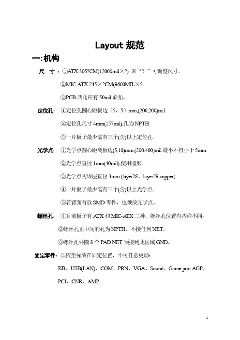
Layout规范一:机构尺寸:①A TX:305?CM(12000mil×?) ※“?”可调整尺寸。
②MIC-A TX:245×?CM(9600MIL×?③PCB四角应有50mil斜角。
定位孔:①定位孔圆心距板边(5,5)mm,(200,200)mil.②定位孔尺寸4mm(157mil),孔为NPTH.③一片板子最少需有三个(含)以上定位孔.光学点:①光学点圆心距离板边(5,10)mm,(200,400)mil.最小不得小于5mm.②光学点直径1mm(40mil),使用圆形。
③光学点防焊层直径3mm.(layer28、layer29 copper)④一片板子最少需有三个(含)以上光学点。
⑤若背面有放SMD零件,也须放光学点。
螺丝孔:①目前板子有A TX和MIC-A TX二种,螺丝孔位置有些许不同。
②螺丝孔正中间的孔为NPTH,不接任何NET。
③螺丝孔外圈8个P AD NET须接到此区域GND。
固定零件:须依坐标放在固定位置,不可任意更动:KB、USB(LAN)、COM、PRN、VGA、Sound、Game port AGP、PCI、CNR、AMP二:Placement顺序: 1.机构零件先摆。
(须用坐标去摆,全部过程中要用键盘,不可用鼠标)2.大零件先摆定:CPU、北桥、南桥、PWM、DIMM、CLK、A TK、A TX-CON、IDE、FDC、Sound\、Super l/O、BIOS3.须看线路图一页一页依据大零件摆零件,不可摆在不相关位置或摆的很远。
在摆同时须依照走线将方向确定,不是摆了就可以。
(有时线路图画在这一页,但不见得就摆在这里,须注意NET的接法)注意事项:1.放置零件时格点需设定为G25,零件原点固定朝左或朝上。
2.零件不可排的过近(外框不可有重迭现象),尤其同是DIP零件如:EC对EC、EC对CHOKE…会使生产加工零件产生挤推,造成零件浮件状况。
AD20设计规则小结(DesignRules)
AD20设计规则⼩结(DesignRules)⼀.Electrical(电器规则)1.Clearence (线间距、铺铜间距设置规则)常规情况下,铺铜间距可设置为线间距的2-3倍;且铺铜间距和线间距应该分开制定规则。
2.Short-Circuit(短路提醒设置)此规则⽤来设计电路⽹络中的短路许可,系统默认规则是不允许短路。
3.Un-Routed Net(不完全连接检查规则)此规则⽤来检查电路⽹络中是否还存在未⾛线的⽹络,系统默认规则是不允许存在未⾛线的⽹络。
4.Un-Connected Pin(不完全连接Pin脚检查规则)此规则⽤来检查电路⽹络中是否存在未连接引脚,此规则⼀般不做设定,系统亦没有默认规则。
5.Modified Polygon(多边形铺铜规则)主要是⽤来防⽌铺铜时,当作出⼤铜⽪套⼩铜⽪的操作时,由于外部更改,重新铺铜后,会容易忽略⼩铜⽪⽽造成粘连。
Unpoured Polygen(未铺铜的多边形)→⑴Allow Shelved(允许隐藏显⽰):属于该规则范围内且当前已搁置的所有多边形将不会被标记违规;⑵Allow Modified(允许修改):属于该规则范围内且当前已修改但尚未铺铜的所有多边形将不会被标记违规;6.Creepage Distance(爬电距离)此规则是⽤来设置两个相邻导体(焊盘)或⼀个导体(焊盘)与相邻电机壳表⾯的沿绝缘层测量的最短距离。
爬电距离是沿绝缘表⾯测得的两个导电零部件之间或导电零部件与设备防护界⾯之间的最短路径。
即在不同的使⽤情况下,由于导体周围的绝缘材料被电极化,导致绝缘材料呈现带电现象。
(百度百科)⼆.Routing(⾛线规则)1.Width(线宽设置)2.Routing Topology(布线拓扑规则)⑴Short(布线最短规则) :在布线时连接所有节点的连线最短规则。
⑵Horizontal(⽔平最短规则):连接所有节点的⽔平连线最短规则。
⑶Vertical(垂直最短规则):连接所有节点的垂直⽅向连线最短规则。
CHIPONE培训资料-集创触控IC选型及项目开发流程介绍

32Bit MCU+DSP
32K Flash 4K SRAM
6*6*0.75 I2C/SPI
Copyright © Chipone Corp. all rights reserved.
2
2013-10-16
各家触控IC介绍 ‐ 敦泰
CONFIDENTIAL
厂商 敦泰
型号
FT5216 FT5316 FT5406
5
互电容
10
互电容
DITO条形、单面跨桥
10
16*10 23*14 23*12
QFN40 QFN48 QFN48
思立微 GSL2682
互电容
单层多点
10
23*12
QFN48
GSL3670 GSL3680 GSL915 GSL960 GSL968
互电容 互电容 互电容 互电容 互电容
DITO条形、单面跨桥
北京集创北方科技股份有限公司
内容
各家IC介绍及替换选型 集创北方触控IC选型表 集创北方触控项目开发流程
CONFIDENTIAL
Copyright © Chipone Corp. all rights reserved.
2013-10-16
各家触控IC介绍‐集创北方
CONFIDENTIAL
厂商
型号
自电容/ 互电容
可以支持图案
触控 通道数 点数 (Tx * Rx)
支持尺寸
ICN8302M 互电容 DITO条形、单面跨桥 5 15*10 2.8"-4.0"
封装类型 QFN40
MCU Flash/RAM
8051+DSP
32K Flash 4K SRAM
layout design

画一个standard cell 最重要的是要小、快、工整,必免不必要的电容效应 ( t= RC )一般而言,要达到小、快、工整最重要的是floor plan,所以在拿到电路图的一开始要先考率清楚输出入的位置再决定layout 的方式一般输出入以 1 对 1 为最常见也最为简单习惯上电路会再修改增加电路都是输出入两部份所以习惯都是将输出入的MOS放置在最两侧以方便未来的modify.其次就是1对多的输出入一般就会考虑它未来会不会再modify成其它的电路部份做优先考虑会的部份一定优先放置最外侧,可能就会将输入放在中间两两对称的输出放置在两侧,如果是多输入一输出,则还是会考虑将输出放置在最外侧以方便未来改size,增加电路优先考虑‧其次是常见的是clock互换电路,也就是 a 和 a_ 的电路其实整个电路是一样的只是clock线互换一般常见错误的 layout 是将clock的 Inverter 放置在电路中间造成由a 改成 a_ 时其它MOS会接不到换线的讯号,或是改用polygate来接线,将会影响clock的讯号速度所以最好floor plan时可以将ck_inverter放置在最外侧,换线时直接改ck_inverter的方向或layout就好了,也没有放置中间时和其它和临近的DRC Rule 问题STD layout 注意事项0. Abut 共享电源端的Source node和所有cell上下左右 1/2 的DRC Rule1. CMOS 间的diffusion 要最近 (如此CMOS反应会快)2. polygate 要少(diffusion 拉近,polygate就会相对减少)3 poly contact area 要最小4 讯号Drain node 的oxide 最好是最小面积,最多contact 数(减少电容效应,并联电阻R//R= 1/2 R)5 接VDD 和 GND的Source node 的面积可大就大点,增加电容量,contact 越多越好,减少电阻( Q=CV C= m* A/l*l)6. 量测好每一个 contact 到 contact间的oxide间距相等,达到电阻值都相同,电流量一致如: .18 制程中的 widthwidth = 1u contact=.22u[1-(0.22*2)]/4=0.14则contact 之间就有.28u间距,contact到oxide edge 就有.14u7 避免用poly gate 接线,可用poly contact 和 metel 换线就换8 .若有折根数的MOS以偶数根为主,信号端放置中间,电源端则放两侧,如此信号端的面积小速度快9 折根后的width 要先考虑9.1 大小根数对称9.2 考虑contact数量如 : z size NMOS width=3.3 ,1.2 和 0.9都可打下2颗co 数 (1) 就会折成 1.2 1.2 0.9 (可打下一颗sub-co)PMOS width=4.8 (打下3颗 co 数)(2) 就会折成 1.7 1.7 1.4(同上)(3) width= 5.0 ~> 1.8 1.8 1.49.3 考虑可以打下一颗substrate 的width10. 画完后,先检查有无Metal绕远路的现像11. 包Metal 是否过多过少 , Metal 线环绕太大圈12. 连接vdd和gnd的Metal 最好是大边对大边包,增加电流量降低电阻值13. 不同讯号和或电位的Metal 间的距离在允许下,能离远就远或分均14 . Metal 包讯号线的contact能大小边就大小边,若能多打contact就采用小边包大边15. poly endcap 一定要最短16. substrate co 最好多打,且最好能作butte,增加电荷量,电流量也会比教多,电阻也小,metal area小17. substrate co 最好接近device18. substrate co 最好贴近prbound region ,确保Abut邻近cell是没有su bstrate的问题19.pin metal 尽量不要和contact 有重迭(overlap)一起,因为该contact 比较容易溶化20.pin metal 尽量不要放置在最上和下一条grid 上,离电源端太近易有噪声电容21.pin metal area 最好是正方形(square),刚刚大小,除非是source 和 dr ian 端,就不必遵循22. ViaBlockage 是要避免Apllo 将pin点出在contact上所加上的保护层,所以只需加在grid可能和contact overlap处就可以23. 多加上的ViaBlockage layer可能会造成 P&R 上的出pin问题,所以不要多加ViaBlackage 在metal 上24. 最后必须check所有cell是flatten 并且是Merge25. check creat contact 内的symbolic 是否被移除(remove symbol)26. check Metal Text 是否和pin metal在一起(在z cell中常发现未在一起)27. check ViaBlockage 和 pin metal 是否overlap28.About其它cell 看看有无DRC Rule29 .check pin metal 下有无metal draw layer,没有要加上30. run program of Caliber's DRC and LVS and ERC31. run program of Random 50000 cell32. 输出端的inverter 的oxide 一定要尽量小,如此输出才快33. 输出端的metal如果可以尽量和metal 包pin一样大,如此电流密度才大34. metal间的间距尽量balance 小可减少metal 电容——IC设计基础(流程、工艺、版图、器件)——1、我们公司的产品是集成电路,请描述一下你对集成电路的认识,列举一些与集成电路相关的内容(如讲清楚模拟、数字、双极型、CMOS、MCU、RISC、CISC、DSP、ASIC、FPGA 等的概念)。
PCB Layout 规范

1.0 目的:提供PCB Layout 時之依據,確保所Layout 之PCB 符合實際生產及相關標準,以期降低生產之困擾,使PCB生產順暢。
2.0適用範圍:本公司生產之CD-ROM 、Mother Board 、DVD -Decoder Card、介面卡等所有產品皆適用之。
3.0定義:3.1 PCB: Printed Circuit Board3.2 Layout: PCB設計製作3.3 Dimension: mm(公制) mil(英制)1mil =0.0254 mm4.0參考資料:4.1IPC-A-600D 印刷電路板允收標準4.2本公司SMT 生產設備Manual5.0相關單位職責:5.1R/D部門:負責PCB設計及規格制訂、並負責与PCB製作廠商之作業要求及技術規範,包括提供所需之文件檔案。
5.2製造單位:負責規格、資訊之提供及問題回饋。
5.3品管單位:負責執行檢驗作業。
6.0作業內容与程序6.1SMT 部分6.1.1 PCB 尺寸規格 mm6.1.2 6.1.2.1規格 1 ---- 圓形D1:1.0 mm (±10%)D2:2.0 mm (±10%)6.1.2.2 規格 2 ---- 正方形D1: 1.0 mm (±10%)D2: 2.0 mm (±10%)6.1.2.3 規格 3 ---- 三角形D1: 1.0 mm (±10%)D2: 2.0 mm (±10%)6.1.2.4 規格 4D1: 1.0 ~ 2.0 mm (±10%)6.1.2.4 規格 4 ---- 十字形D1: 1.0 mm (±10%)D2: 2.0 mm (±10%) LT6.1.2.5規格5 ---- 貫穿孔作markD1: 1.0 mm (±10%)D2: 2.0 mm (±10%)6.1.2.6 規格6 ----PAD作markD1: 1.0 mm (±10%)D2: 2.0 mm (±10%)6.1.2.7 Layout 時須注意事項6.1.2.7.1 PCB上至少應有三個Fiducial Mark ,若為雙面SMT則每面各要有三個以上。
LCM Layout绘制说明PPT课件
为保护金手指需要在每个金手 指端拉出过孔线,且过孔不能 在一条直线上(避免弯折出现 整条金手指折断脱落)应高低 交错排列。且金手指两面均需 连线到过孔,可防止金手指一 边断裂后另一边仍有线路连接。
52
如图即为走线完成后 的图面,需注意走线 尽量避免直角,所有 角度走线需进行圆弧 修正,避免尖端放电
换外形类型
36
设置为如图参数, 类型为Copper,点 击OK退出对话框
选择端子右键选择 Associate进行属性连接
37
因需要进行补强,所以 需再增加0.3的铜片。
点击Copper进行增加 增加Copper区然 后进行属性连接
38
如图即为设置完 成后图面,然后
进行保存
保存时命名一定 要与Logic设计中 的封装命名一致
Layout绘制说明
2010-12-29 Willis
整体 概述
一 请在这里输入您的主要叙述内容
二
请在这里输入您的主要 叙述内容
三 请在这里输入您的主要叙述内容
2
Layout前准备
1、Logic原理图完成 2、LCM机构图档,FPC机构图档及DXF文件
3
双击图标
进入PADS Layout编辑界面
25
进入颜色编辑对话框进行显 示刚才复制进来的机构外形, 完成后点击OK退出对话框。
26
设置元件封装的原点,如图 设置为原件起始PIN的左下角。
27
点击图标选择封装设计工具栏。
28
点击图标选择新建电性端子, 如红色的即为新建的电性端子。
29
选择电性端子右键选择属性 Quary/Modify进行属性设置。
对话框。
17
点击Setup选择Set Origin, 进行图面原点设置。
PWM 等 电源管理 PCB Layout Guidelines

SIMPLE SWITCHER ®PCB Layout GuidelinesIntroductionOne problem with writing an Application Note on PCB layout is that the people who read it are usually not the ones who are going to use it.Even if the designer has struggled through electromagnetic fields,EMC,EMI,board parasitics,transmission line effects,grounding,etc.,he will in all prob-ability then go on with his primary design task,leaving the layout to the CAD/layout person.Unfortunately,especially when it comes to switching regulators,it is not enough to be concerned with just basic routing/connectivity and mechani-cal issues.Both the designer and the CAD person need to be aware that the design of a switching power con-verter is only as good as its layout.Which probably ex-plains why a great many of customer calls received,con-cerning switcher applications,are ultimately traced to poor layout practices.Sadly,these could and should have been avoided on the very first prototype board,saving time and money on all sides.The overall subject of PCB design is an extremely wide one,embracing several test/mechanical/production issues and also in some cases compliance/regulatory issues.There is also a certain amount of physics/electromagnetics involved,if a clearer understanding is sought.But the purpose of this Application Note is to reach the audience most likely to use it.Though there is enough design information for the moreexperienced designer/CAD person,the Application Note in-cludes a quick-set of clear and concise basic rules that should be scrupulously followed to avoid a majority of prob-lems.In particular,we have provided recommended start-ing points for layout when using the popular LM267x,LM259x and LM257x families (Figure 2)The focus is on the step-down (Buck)Simple Switcher ICs from National,but the same principles hold for any topology and switching power application.Most of the issues discussed in this Note revolve around simply assuring the desired performance in terms of basic electrical functionality.Though luckily,as the beleaguered switcher designer will be happy to know,in general all the electrical aspects involved are related and point in the same general ‘direction’.So for example,an ‘ideal’layout,i.e.one which helps the IC function properly,also leads to reduced electromagnetic emissions,and vice-versa.For example,reducing the area of loops with switching currents will help in terms of EMI and performance.However the designer is cautioned that there are some exceptions to this general ’trend’.One which is brought out in some detail here is the practice of ’copper-filling’,which may help reduce parasitic inductances and reduce noise-induced IC problems,but can also increase EMI.Quick-Set of Rules for SIMPLE SWITCHER PCB Layout (Buck)a)Place the catch diode and input capacitor as shown in Figure 2.b)For high-speed devices (e.g.LM267x)do not omit placing input decoupling/bypass ceramic capacitor (0.1µF–0.47µF)as in Figure 2.c)Connect vias to a Ground plane if available (optional,marked ‘X’in Figure 2)d)If vias fall under tab of SMT power device,these are considered ‘thermal vias’.Use correct dimensions as discussed to avoid production issues.Or place the vias close to but not directly under the tab.e)Route feedback trace correctly as discussed,away from noise sources such as the inductor and the diode.f)Do not increase width of copper on switching node injudiciously.g)If very large heatsink area is required for catch diode (having estimated the heatsink requirement correctly)use isolation as discussed.h)For higher power SMT applications,use 2oz board for better thermal management with less copper area.SIMPLE SWITCHER is a Registered Trademark of National Semiconductor.National Semiconductor Application Note 1229Sanjaya Maniktala July 2002SIMPLE SWITCHER PCB Layout GuidelinesAN-1229©2002National Semiconductor Corporation Introduction(Continued)The AC and DC Current PathsReferring to Figure 1a ,the bold lines represents the main (power)current flow in the converter during the time the switch is ON.As the switch turns ON,the edge of the of the current waveform is provided largely by CBYPASS,the re-mainder coming mainly from CIN.Some slower current com-ponents come from the input DC power supply (not shown)and also refresh these input caps.Figure 1b represents the situation when the switch is OFF.We can therefore see that in certain trace sections,current has to start flowing sud-denly during the instant of switch turn-off and in some sec-tions it needs to stop flowing equally suddenly.Figure 1c represents the ‘difference’,i.e.traces shown bold in this Figure are those where the current flow changes suddenly .During the turn-on transition the picture reverses,but the ’difference’trace sections are the same.Therefore during either switch transition,’step changes’of current take place in these difference sections.These traces encounter the harmonic-rich rising or trailing edges of the current pedestal waveform.The difference traces are considered ’critical’and deserve utmost attention during PCB layout.It is often stated colloquially,that ‘AC current’flows in these trace sections,and ’DC current’in the others.The reason is that the basic switching PWM frequency forms only a fraction of the total harmonic (Fourier)content of the current waveform in the ’AC’traces.In comparison,where ‘DC current’flows,the current does not change in a stepped fashion and so the harmonic content is lower.It is also no surprise that the DC20042601FIGURE 1.A N -12292The AC and DC Current Paths (Continued)sections are those in series with the main inductor,because it is known that inductors have the property of preventing sudden changes in current(this is analogous to a capacitor which‘resists’sudden changes in voltage).Summing up:In switching regulator layout,it is the AC paths that are considered critical,whereas the DC paths are not.That is the only basic rule to be kept in mind, and from which all the others follow.This is also true for any topology.Perform an analysis of the current flow for any topology in the same manner as we did for the Buck,to find the’difference traces’:and these traces are by defintion the’critical’ones for layout.What is the problem with step current changes anyway?In a resistor for example,this causes no unexpected/ unidentifiable problem.The voltage is given by V=IR,and so for a given change of current,the voltage will change pro-portionally.For example,a0.5cm wide Cu trace of thick-ness1.4mil has a resistance of1milliohm per cm length (at20degC).So it seems that a1inch long trace with a current changeover of1A,would produce a change in volt-age of only2.5millivolts across the trace,which is insignifi-cant enough to cause the control sections of most ICs to misbehave.But in fact the induced voltage is much larger. The important thing to realize is that traces of copper on a PCB,though barely resistive,are also inductive.Now,the oft-repeated thumb-rule is that‘every inch of trace length has an inductance of about20nH’.Like the trace resis-tance,that too doesn’t seem much at first sight.But it is this rather minute inductance which is in fact responsible for a great many customer calls in SIMPLE SWITCHER applica-tions!The equation for voltage across an inductance is V=L*dl/dt, and so the voltage does not depend on the current but on the rate of change of the current.This fact makes all the differ-ence when the1A change we spoke about occurs within a very short time.The induced voltage can be very high,even for small inductances and currents,if the dl/dt is high.A high dl/dt event occurs during transition from Figure1a to Figure 1b(and back)in all the AC trace sections(shown bold in Figure1c).The induced voltage spike appears across each affected trace,lasting for the duration of the crossover.To get a better feel for the numbers here:the change in current in the AC sections of a typical buck converter is about 1.2times the load current during the switch turn-off transition and is about0.8times the load current during the switch turn-on transition(for an’optimally’designed Buck inductor,as per inductor design guidelines in the relevant Datasheets/Selection Software).The transition time is about30ns for high speed Fet switchers like the LM267x,and is about75ns for the slower bipolar switchers like the LM259x series.This also incidentally means that the voltage spikes in the high-speed families can be more than twice that in the slower families,for a comparable layout and load.Therefore layout becomes all the more critical in high-speed switchers.So,one inch of trace switching say1A of instantaneous current in a transition time of30ns gives0.7V,as compared to 2.5mV(that we estimated on the basis of resistance alone).For3A,and two inches of trace,the induced voltage ’tries’to be4V!In Figure1c,the small triangles along the sections indicate the direction of the momentary induced voltage,as the converter changes from the situation in Fig-ure1a to that in Figure1b(switch turn-off).We can see thatassuming that the ground pin of the IC is the reference point,the switching node(marked‘SW’)tries to go negative(all itsseries trace sections adding up).Similarly the input pin(marked‘VIN’goes high through series contributions in all itsrelated sections.Figure1c represents the picture during theturn-off transition.During the turn-on transition all the in-duced voltage polarities shown are simply reversed.In thatcase,the VIN pin is dragged low,and the switching node pinis dragged high momentarily.The astute designer will recognize that this was to be ex-pected since any inductance,even if it is parasitic,demandsto be‘reset’,which means that the volt-seconds during theon-time must equal and be opposite in sign to thevolt-seconds during the off-time.The designer will also real-ize that till these parasitic trace inductances reset,they donot’allow’the crossover to occur.So for example,traceswhich were carrying current prior to switch turn-off will’insist’on carrying current till the voltage spikes force them to dootherwise.Similarly,the traces which need to start carryingcurrent will’refuse’to do so till the spikes across them forcethem to do likewise.Since switching losses are proportionalto crossover time,even if these voltage spikes do not causeanomalous behavior,they can degrade efficiency.For ex-ample,in transformer-based flyback regulators,when the theprimary number of turns is much larger than the secondaryturns,designers may be surprised to learn how much thesecondary side trace inductances alone can degrade effi-ciency.This is because any secondary side uncoupled(trace/transformer leakage)inductances reflect into theprimary side as an equivalent parasitic inductance inseries with the switch.This adds an additional term tothe effective leakage as seen by the switch that equalsthe secondary inductance multiplied by square of theturns ratio(turns ratio being Np/Ns).Therefore the dissipa-tion in the flyback clamp(zener/RCD)can increase dramati-cally,lowering efficiency.One lesson here is that though’leakage inductance’(from traces or the transformer)is con-sidered’uncoupled’,in reality it can make its presence se-verely felt from one side of the transformer to the other.So itis not totally’uncoupled’at all!In fact this happens to be themain reason why flybacks with low output voltages(highturns ratio)show poorer efficiency as compared to higheroutput flybacks.Therefore,reducing critical trace induc-tances is important for several reasons:efficiency,EMI,be-sides basic functionality.The momentary voltage spikes which last for the duration ofthe transition can be very hard to capture on an oscilloscope.But they may be presumed to be present if the IC is seen tobe misbehaving for no’obvious reason’.These spikes,ifpresent with sufficiently high amplitude,can propagate intothe control sections of the IC causing what we call here acontroller’upset’.This leads to the observed performanceanomalies,and in rare cases this can even cause devicefailure.Since none of these spike-related problems can beeasily corrected,or band-aided,once the layout is initiallybad,the important thing is to get the layout‘right’to startwith.The designer may well ask,why is it that these step currentchanges are a problem with the parasitic trace inductances,and not with the main inductor of the Buck converter?That isbecause all inductors try to resist any sudden currentchange.But since the main inductor has a much largerinductance(and energy storage)as compared to the para-sitic trace inductances,it therefore ends up‘dominating’.From V*dt=L*dl we can also see that if L is large,a muchhigher voltseconds(V*dt)is required to cause a givenAN-12293The AC and DC Current Paths(Continued)change in current.The trace inductances therefore simply ’give in’first before the main inductor does.But they certainly don’t go down without a fight...and the voltage spikes bear testimony to this!Notice that the currents in the signal traces in the schematic are not shown.For example those connected to the com-pensation node (marked ‘COMP’)or bootstrap (marked ‘BOOST’)carry relatively minute currents and therefore are not likely to cause upsets.They are therefore not critical and can be routed relatively ‘carelessly’.The feedback trace is an exception,and will be discussed later.The Ground pin of the IC is another potential entry point of noise pickup.Inex-perienced designers often grossly under estimate the needs of this pin,particulary for Buck converters.They assume that since the main power flow in a Buck converter does not pass through the ground pin,the ‘current through the ground pin is very low’,and therefore the trace length leading up to this pin is not critical.In fact,though the average current through this pin is very low,the peak current or its dl/dt is not.Consider the switch driver as shown schematically in Figure 1.Clearly it needs to supply current to drive the switch.In any Fet operated as a switch,large peak to peak instantaneous current spikes are needed to charge and discharge the gate capacitance.This is essential so as to cause the Fet to switch fast,and this reduces the switching/crossover losses inside the switch and improves the overall efficiency of the converter.(Actually,in a practical IC,the ‘spike’of current comes from the bootstrap capacitor,and then the bootstrap capacitor is quickly refreshed by the internal circuitry of the IC ----it is the refresh current that passes through the ground pin).Further,as in any high-speed digital IC,parts of the internal circuitry,clocks,gates,comparators etc.,can turn on and off suddenly,leading to small but abrupt changes in the current through the ground pin.This can cause ’ground bounce’which in turn can lead to controller upsets.There-fore the length of the trace to the Ground pin also needs to be kept as small as possible.This also implies that the input capacitors,especially the bypass capacitor ‘CBYPASS’should be placed very close to the IC ,even for a Buck IC.Placing Components ‘acap’(as Close as Possible)One has heard this before:“component X needs to be ‘acap’”.Soon we are told the “component Y too needs to be ‘acap’”.Then “Z too”.And so on.Which would be physically impossible because matter cannot occupy the same place at the same time!So which one comes first?This is the million-dollar predicament always facing switcher layout.The troubling trace lengths are those indicated Figure 1c .To keep them small,clearly two components need to be acap.These are the input bypass capacitor and also the catch diode.Consider the input capacitor section first.In the schematic there are in two input capacitors shown.These are marked ‘CIN’and ‘CBYPASS’respectively.The purpose of the total input capacitance is to reduce the volt-age variations at the input pin.The variations are mainly due to the pulsed input current waveshape,as demanded by a Buck topology.Note that for this particular topology,the output capacitor current is smooth (because the inductor is in series with it).In a Boost topology the situation is re-versed:i.e.the input capacitor current is smooth and the current into the output capacitor is pulsed.This makes thedemand for input decoupling less stringent than in a Buck (or Buck-Boost).In a Buck-Boost or ’flyback’,both the input and the output capacitor currents are pulsed,and input decou-pling is required not only for the control-section/drivers of the IC but for the input current step waveform of the power stage.Designers familiar with a Cuk topology know that in this case both input and output currents are smooth.The Cuk converter is therefore often called the ’ideal DC to DC’converter,and expectedly its parasitic inductances can be largely ignored ----because there are no AC trace sections in the sense we described.Now if the input power to a Buck converter was coming through long leads from a distant voltage source,the induc-tance of the incoming leads would seriously inhibit their ability to provide the fast changing pulsed current shape.So an on-board source of power is required right next to the converter,and this is provided by the input capacitor.It provides the pulsed current,and then is itself refreshed at a slower rate (DC current)from the distant voltage source.However,since the input capacitor is fairly large in size,it may not be physically possible to place it as close as de-sired.Especially for very high speed switchers such as the LM267x series (note that a ‘high speed’switcher as de-fined here,is one with a very small crossover/transition time,and it does not necessarily have to be one with a high switching frequency ).In addition,the Equivalent Se-ries Resistance (‘esr’)and Equivalent Series Inductance (‘esl’)of the main input capacitor may be too high,and this can cause high frequency input voltage ripple on the VIN pin.For the Buck converter schematic as shown in Figure 1,the input pin connects not only to the Drain of the Fet switch,but also provides a low internally regulated supply rail to the control sections of the IC.But no real series pass regulator can ’hold off’very fast changes in the applied input voltage.Some noise will feed through into the control section and then much will depend on the internal sensitivity of the IC to noise (related to its design,internal layout,process/logic family).It is therefore best to try to keep voltage on the VIN pin fairly clean --—from a high frequency point of view.Note that it is not being suggested here that one responds to this statement by increasing the input capacitance indiscrimi-nately,because we are not talking about the natural input voltage ripple which occurs at the rate of the switching frequency (e.g.100kHz–260kHz).Our concern here is the noise occurring at the moment of the transitions,and this noise spectrum peaks at around 10MHz–30MHz,as deter-mined by the transition/crossover time of the switch.The crossover time has nothing to do with the basic PWM switch-ing frequency,but does ofcourse depend on the type of switch used i.e.bipolar or Fet.Therefore a high frequency ‘bypass’or ‘decoupling’capacitor with small or no leads,shown as ‘CBYPASS’in Figure 1,is to be placed very close to the VIN and GND pins of the IC.This is usually a 0.1µF–0.47µF (monolithic)multilayer ceramic (typically X7R type,size 1206or the more recent ’inverted’termination version of this popular size,the ’0612’----also note that smaller sized ceramic caps generally have higher esr/esl,but check before use).Since now this com-ponent provides the main pulsed current waveshape,the bulk capacitor shown as ‘CIN’,may be moved slightly further up (about an inch)without any deleterious effect.For lighter loads,and if it is possible to place the input bulk capacitor very close to the IC,the high frequency bypass capacitor may sometimes be omitted.But for high-speed switchers like the LM267x,the input ceramic bypass capacitor is considered almost mandatory for any application.A N -12294Placing Components‘acap’(as Close as Possible)(Continued)The position of the catch diode is also critical.It too needs to be acap.Now,every topology has a node called the’switch-ing node’.This is the’hot’or’swinging’end of the switch.For integrated switchers,this node can also be an easy entry point for noise feed-through into the control sections.Note that the problem is not caused by the simple fact that the voltage at this node swings,for it is designed for exactly that situation in mind.The problem is with the additional noise spikes riding on top of the basic square voltage waveform, arising from the trace inductances as explained earlier. Therefore,it is essential to place the catch diode very close to the IC and connect it directly to the SW pin and GND pins of the IC,with traces that are very short and fairly wide.In some erroneous layouts,where the catch diode was not appropriately placed to start with,the con-verter could be‘bandaided’by a small series RC snubber. This consists typically of a resistor(low inductive type preferred)of value10Ω–100Ωand a capacitor,which should be ceramic of value470pF–rger capaci-tance than this would lead to unacceptably higher dissipation (=1/2*C*V2*f),chiefly in the resistor,and would serve no additional purpose.However,note that this RC snubber needs to be placed very close to and across the Switch-ing pin and Gnd pin of the IC,with short leads/traces. Sometimes designers think that this is’across the diode’, because on the schematic there is no way to tell the differ-ence.However,particularly when the diode is a Schottky,theprimary purpose of such a snubber is to absorb the voltagespikes of the trace inductances.Therefore its position mustbe such that it provides bypassing of the critical or AC tracesections of the output side as shown in Figure1c(right handside of the switcher)----which means it must be close to theIC.Of course,as mentioned previously,it is best to get thelayout right to start with,rather than adding such extracomponents.Remaining component placements can be taken up onlyafter the input bypass capacitor and the catch diode arefirmly in place and are both acap.The traces to either ofthese two components should be short,fairy wide,andshould not go pass through any vias on the way to the IC.For SMT boards this implies that the input capacitor andcatch diode are on the same layer as the IC.In Figure2suggested PCB starting points are provided for severalswitchers.All of them focus on placing these two criticalcomponents correctly.These layouts are strongly recom-mended for most applications.The’X’marks suggest therecommended location where vias can be used to con-nect to a Ground Plane(if present).The remaining compo-nents can be placed relatively carelessly(though in doing so,there may be slight impact,for example on the accuracy ofthe output voltage rail and its ripple,but nothing compared towhat can happen if the input decoupling cap and catch diodeare incorrectly placed).Trace routing is now discussed inmore detail.AN-12295Placing Components ‘acap’(as Close as Possible)(Continued)Routing the TracesAs mentioned above,it is not advisable to route any of the critical traces through ‘vias’.Vias are considered useful from a purely CAD perspective for ‘layer jumping’,but are often used indiscriminately as they seem an easy solution to con-nectivity problems.But they also add impedance,and that is exactly what we are trying to avoid.The inductance of a via is given bywhere ‘h’is the height of the via in mm (equal to the thick-ness of the board,commonly 1.6mm),and ‘d’is the diam-eter in mm.Therefore a single via of diameter 0.4mm on a standard 1.6mm board gives an inductance of 1.2nH.It may not sound much,but it is almost twice that of a wire of the same length and diameter.It has been seen empirically that for the high speed LM267x series,if the bypass capacitor is connected through vias to the IC,occa-sional field problems do arise.So if vias have to be usedfor some reason,several vias in parallel will yield better results than a single via.And larger via diameters would help further (unless they are being used as ’thermal vias’---discussed later).It is also said that “the traces also need to be ‘wide’and ‘short’”.The necessity of short traces is clearly understood,usually intuitively,by most engineers.In fact the thumbrule of ‘20nH per inch’also implies that trace inductance is almost proportional to length.However,a common ‘intuitive’mis-take is to assume that inductance is inversely propor-tional to the width of the trace .So some engineers mis-takenly ‘add copper’lavishly to critical traces (though there are some other reasons why this may be being done,and these will be discussed later).A first approximation for the inductance of a conductor having length ‘l’and diameter ‘d’iswhere l and d are in centimeters.Note that the equation for a PCB trace is not much different from that of a wire.20042602FIGURE 2.Recommended Layout Starting PointsA N -1229 6Routing the Traces(Continued)where ‘w’is the width of the trace.For PCB traces,L hardly depends on the thickness of the copper (1oz or 2oz board).Both the above equations are plotted in Figure 3.It will be seen that for a given length,a PCB trace of width ‘x’has higher inductance than a wire of diameter ‘x’.In fact the width of a PCB trace has to be about 1.78times the diameter of a wire for the same inductance .A wire of AWG 20has a diameter of 32mils (or 0.081cm).So for a length of one inch (1000mils or 2.54cm)L equals 21nH (which is the usual thumbrule).We can see that L is almost proportional to length.But if we double the diameter to 0.16cm,L equals 17nH,which is not much different from 21nH.This indicates a non-linear relationship.Referring to Figure 3,where the above function is plotted out (dotted lines are for a PCB trace),we can see that the diameter/width of a wire/trace has to typically increase by a factor of 10for the inductance to halve .The rela-tionship of L to d is therefore logarithmic in nature.The reason for this is the effects of mutual inductance between parallel sections/strips of the conductor.‘Beefing up’traces to reduce the effects of parasitic induc-tances should be a last resort.Decreasing the length of the trace should be the first step.Increasing the width of certain traces can in fact become counterproductive.In particular,the trace from the switch node to the diode is ‘hot’from an EMI point of view.This is not only because of the AC (high frequency)current it carries,but because of its voltage,which is a switched waveform.Any conductor with a varying voltage,irrespective of the current,becomes an antenna if its dimensions are large enough.Radiated emissions from this antenna can cause undesirable common-mode interfer-ence in its vicinity.Therefore this calls for the area of the copper around the switching node to be reduced,not rge planes of switched voltage also cause ca-pacitive noise coupling into nearby traces.On a typical SMT board,if the opposite side happens to be a ’ground plane’,noise from the switching node can couple through the FR4dielectric of the PCB into the Ground plane.No Groundplane is ’perfect’,and therefore this injected high frequency noise can also cause the ground plane to not only radiate,but to pass noise onto the IC through ’ground bounce’.Some people suggest that a copper island,exactly the same size/shape as the switching-node island be created on the oppo-site side of the PCB,connected through several vias.This is supposed to prevent ’capacitive cross-talk’to other traces and to enhance thermal dissipation.But this obviously also leads to the breaking-up/partioning of the Ground plane.This defeats the very purpose of Ground plane as it can cause strange effects arising due to the odd current flow patterns in the now divided Ground plane.In general,the Ground plane should be kept continuous/unbroken as far as possible,or it could behave like a slot antenna.For the switching node therefore,the best option is to keep the amount of copper around it to the actual minimum re-quirement.Some basic physics to be reminded of here:electric fields are caused by electric charge,and magnetic fields by cur-rents.But if an electric field varies with time,it produces a corresponding magnetic field.However magnetic fields are associated with currents.Therefore AC voltages (varying electric fields)on opposite planes of copper on a PCB cause a ’displacement current’(capacitive coupling current)through the FR4dielectric.Similarly,a varying magnetic field causes an electric field.So for example in a transformer,when we pass AC current (varying magnetic field)in a wind-ing,we get Faraday induced voltages (electric field).When-ever voltage or current is switched,an electromagnetic field is generated,which produces EMI.And this EMI is inadvert-ently ’helped’by antenna structures.Therefore,on a PCB layout,the area enclosed by all current loops carrying ’AC (switched)current’must be kept small.Similarly the area of copper planes with ’AC (switched)voltage’must be kept small.Both can behave as antennae.In addition,traces carrying switching currents/voltages must also be kept away from ’quieter’traces to avoid cross-coupling.Further,since ’sharp edges’are known to cause an increase in field strengths,two 45degree bends in a trace are preferred to a single 90degree bend.Copper Filling:when to StopAdding copper lavishly to traces serves some purpose oc-casionally,sometimes none at all,and sometimes it even works against the design in an unintended manner.There may be no simple hard and fast rules here.Judiciousness needs to be applied.But first it is instructive to consider some of the ‘reasons’why copper is lavished,and to the degree it is really required.Most often the requirements are actually much less than predictions based on ’gut instinct’:We will take each of these separately:A)CURRENT HANDLING CAPABILITYIf we multiply the width of a trace with its thickness we get the ‘cross sectional area’of the conductor.This determines the resistance (per unit length)of the conductor and the consequent self-heating.This leads to an estimable tem-perature rise.It is important to note that the ‘current handling capability’is therefore not a ‘stake in the ground’as some people think,but is related to a permissible temperature rise.20042606FIGURE 3.Inductance of Wire of Length ‘1’AN-12297。
IC Layout Design Rule

Poly
场氧
场氧
poly
场氧 SiO2
Pwell Nwell Nwell SiO2 P-type Si
华侨大学厦门专用集成电路系统重点实验室
Copyright by Huang Weiwei
华侨大学厦门专用集成电路系统重点实验室
Copyright by Huang Weiwei
本章主要内容
版图层次定义
Layout
版图设计规则 简单反相器版图
华侨大学厦门专用集成电路系统重点实验室
Copyright by Huang Weiwei
版图层次定义
Layout 1. 有源区 2.N阱 3. 场注入 4. 正常Vth沟道注入 5. 低Vth NMOS沟道注入 6. 低VthPMOS沟道注入 7. 耗尽型NMOS沟道注入 8. 耗尽型PMOS沟道注入 Active NWell ----------------LVN LVP VDN VDP PS ND PD TO TB PT BC
华侨大学厦门专用集成电路系统重点实验室
Copyright by Huang Weiwei
版图层次定义
Layout 17. 金属1 18.M1和M2接触孔 19. 金属2 20. M2和M3接触孔 21. 金属3 22. 焊盘PAD Metal1 VIA1 Metal2 VIA2 Metal3 PAD A1 W1 A2 W3 A3 CP
版图层次定义
有源区
光刻胶
光刻胶 Si3N4 SiO2
Nwell SiO2 P-type Si
华侨大学厦门专用集成电路系统重点实验室
Copyright by Huang Weiwei
版图层次定义
有源区 封闭图形外形成LOCOS
DesignCompile使用说明之一

Design Compile使用说明孙枫叶一.软件说明Design Compile是synopsys的综合软件,它的功能是把RTL级的代码转化为门级网表。
综合包括转译(Translation),优化(Opitimization),映射(Mapping)三个过程。
在转译的过程中,软件自动将源代码翻译成每条语句所对应的功能模块以及模块之间的拓扑结构,这一过程是在综合器内部生成电路的布尔函数的表达,不做任何的逻辑重组和优化。
优化:基于所施加的一定时序和面积的约束条件,综合器按照一定的算法对转译结果作逻辑优化和重组。
在映射过程中,根据所施加的一定的时序和面积的约束条件,综合器从目标工艺库中搜索符合条件的单元来构成实际电路。
DC有两种界面,图形界面通过敲入design vision&调用出来,另一种命令行界面通过dc_shell-t调用。
建议初学者使用图形界面,因为图形界面比较容易上手;业界的人士比较青睐命令行界面,因为其所耗的资源少,并且将所用的命令写成综合脚本的形式,便于查阅。
因为门级和代码级不同,代码级考虑的是理想情况,但是实际电路不是这样的,它有门级的延时,线的延时,信号的转换时间,甚至时钟信号到达各个触发器的时间不相等。
基于这些考虑,DC通过施加约束,模拟实际环境,根据实际情况得出门级网表。
因此如何适当的施加约束是DC的关键所在。
二.库的配置通过上述说明可知,DC需要通用库和工艺库的支持,DC用到的工艺库是.db或者是.lib格式的,其中.lib格式的文件是可读得,通过此文件可以了解库的详细信息,比如说工作电压,操作温度,工艺偏差等等。
.db格式的库是二进制的,不可读。
.db格式的库由.lib格式的库通过命令read_lib生成。
目标工艺库(Target_library):是指将RTL级的HDL描述到门级时所需的标准单元综合库,它是由芯片制造商(Foundry)提供的,包含了物理信息的单元模型。
版图设计规则

设计规则(design rule)
版图几何设计规则可看作是对光刻掩模 版制备要求。光刻掩模版是用来制造集 成电路的。这些规则在生产阶段中为电 路设计师和工艺工程师提供了一种必要 的信息联系。
• 版图的设计有特定的规则,规则是集成 电路制造厂家根据自已的工艺特点而制定 的。因此,不同的工艺就有不同的设计规 则。设计者只有得到了厂家提供的规则以 后,才能开始设计。
第七页,编辑于星期三:二十点 分。
设计规则(design rule)
两种规则: (a) 以λ(lamda)为单位的设计规则—相对单位 (b) 以μm(micron)为单位的设计规则—绝对单位 如果一种工艺的特征尺寸为S μm,则λ=S/2 μm, 选用λ为单位的设计规则主要与MOS工艺的成比例缩 小有关。
第二十页,编辑于星期三:二十点 分。
Layer Processing(层处理命令)
•层处理命令的类型
第二十一页,编辑于星期三:二十点 分。
Layer Processing(层处理命令)
•Logical Commands(逻辑命令)
ndiff poly Original layer
第二十二页,编辑于星期三:二十点 分。
第九页,编辑于星期三:二十点 分。
设计规则(design rule)
•TSMC_0.35μm CMOS工艺中各版图层的线条最小宽度
第十页,编辑于星期三:二十点 分。
设计规则(design rule)
2、最小间距(minSep) 间距指各几何图形外边界之间的距离。
第十一页,编辑于星期三:二十点 分。
;多晶硅
W1 = geomOr( "W1" )
layout(集成电路版图)注意事项及技巧总结
Layout主要工作注意事项画之前的准备工作与电路设计者的沟通Layout 的金属线尤其是电源线、地线保护环衬底噪声管子的匹配精度一、layout 之前的准备工作1、先估算芯片面积先分别计算各个电路模块的面积,然后再加上模块之间走线以及端口引出等的面积,即得到芯片总的面积。
2、Top-Down 设计流程先根据电路规模对版图进行整体布局,整体布局包括:主要单元的大小形状以及位置安排;电源和地线的布局;输入输出引脚的放置等;统计整个芯片的引脚个数,包括测试点也要确定好,严格确定每个模块的引脚属性,位置。
3、模块的方向应该与信号的流向一致每个模块一定按照确定好的引脚位置引出之间的连线4、保证主信号通道简单流畅,连线尽量短,少拐弯等。
5、不同模块的电源,地线分开,以防干扰,电源线的寄生电阻尽可能较小,避免各模块的电源电压不一致。
6、尽可能把电容电阻和大管子放在侧旁,利于提高电路的抗干扰能力。
二、与电路设计者的沟通搞清楚电路的结构和工作原理明确电路设计中对版图有特殊要求的地方包含内容:(1)确保金属线的宽度和引线孔的数目能够满足要求(各通路在典型情况和最坏情况的大小)尤其是电源线盒地线。
(2)差分对管,有源负载,电流镜,电容阵列等要求匹配良好的子模块。
(3)电路中MOS管,电阻电容对精度的要求。
(4)易受干扰的电压传输线,高频信号传输线。
三、layout 的金属线尤其是电源线,地线1、根据电路在最坏情况下的电流值来确定金属线的宽度以及接触孔的排列方式和数目,以避免电迁移。
电迁移效应:是指当传输电流过大时,电子碰撞金属原子,导致原子移位而使金属断线。
在接触孔周围,电流比较集中,电迁移更容易产生。
2、避免天线效应长金属(面积较大的金属)在刻蚀的时候,会吸引大量的电荷,这时如果该金属与管子栅相连,可能会在栅极形成高压,影响栅养化层质量,降低电路的可靠性和寿命。
解决方案:(1)插一个金属跳线来消除(在低层金属上的天线效应可以通过在顶层金属层插入短的跳线来消除)。
IClayout布局经验总结
IClayout布局经验总结第一篇:IC layout布局经验总结IC layout布局经验总结布局前的准备: 1 查看捕捉点(grid)设置是否正确.08工艺为0.1,06工艺为0.05,05工艺为0.025.2 Cell名称不能以数字开头.否则无法做DRACULA检查 3 布局前考虑好出PIN的方向和位置布局前分析电路,完成同一功能的MOS管画在一起对两层金属走向预先订好。
一个图中栅的走向尽量一致,不要有横有竖。
对pin分类,vdd,vddx注意不要混淆,不同电位(衬底接不同电压)的n井分开.混合信号的电路尤其注意这点.在正确的路径下(一般是进到~/opus)打开icfb.8 更改cell时查看路径,一定要在正确的library下更改,以防copy过来的cell是在其他的library下,被改错.9 将不同电位的N井找出来.布局时注意: 完成每个cell后要归原点 DEVICE的个数是否和原理图一至(有并联的管子时注意);各DEVICE的尺寸是否和原理图一至。
一般在拿到原理图之后,会对布局有大概的规划,先画DEVICE,(DIVECE之间不必用最小间距,根据经验考虑连线空间留出空隙)再连线。
画DEVICE后从EXTRACTED中看参数检验对错。
对每个device器件的各端从什么方向,什么位置与其他物体连线必须先有考虑(与经验及floorplan的水平有关)如果一个cell调用其它cell,被调用的cell的vssx,vddx,vssb,vddb如果没有和外层cell连起来,要打上PIN,否则通不过diva检查.尽量在布局低层cell时就连起来尽量用最上层金属接出PIN。
接出去的线拉到cell边缘,布局时记得留出走线空间.16 金属连线不宜过长; pT/R7NU 17 电容一般最后画,在空档处拼凑。
18 小尺寸的mos管孔可以少打一点.19 LABEL标识元件时不要用y0层,mapfile不认。
IC LAYOUT 设计基础
常见操作:
▪ 打散单元:EDIT->HIERARCHY->FLATTEN>FLATTEN PCELLS
▪ 完成版图后标端口:CREAT->PINS FROM LABLES
VIA等时,可能会因为位置摆放问题导致最小 线宽不符合要求。 ▪ 最小间距:不仅要注意各层自己的间距,如 METEL1与METEL1连线间间距,还要注意不 同层之间间距符合设计规则。 ▪ 最小包围:由于要满足内层的最小宽度以及外 层与内层的最小包围,因此在连接部分等处要 求内层材料比原先宽度增加一些。
如把一个管子拆成两个如把一个管子拆成两个可以可以ababbaba的方式的方式如果有四个管子可以各拆成三个用如果有四个管子可以各拆成三个用abcdabcdabcdabcdabcdabcd的方式的方式使器件保持同一方向使器件保持同一方向选择一个中间值作为根部件选择一个中间值作为根部件采用指状交叉方式采用指状交叉方式四方交叉的成对器件四方交叉的成对器件虚拟器件虚拟器件注意临近器件注意临近器件对敏感线来说至少要做到的是在它的走线过程对敏感线来说至少要做到的是在它的走线过程中尽量没有其他走线和它交叉
5.常见器件:
▪ MOS器件:
MOS器件的属性:
二极管
三极管
电容
电感
电阻:
电阻的属性
PAD:
6.层次的介绍
▪ LAYOUT中需要设计各个层次。前面已经 说过,版图是指在半导体工艺制造过程之 前,将工艺进程中的各个步骤所需要用到 的掩膜板形状用层次的概念反映出来的一 种图形。那么,才版图中究竟有多少层次? 最常用的一些层次是什么?
集成电路 DESIGN-RULE文件认知 教学PPT课件

DESIGN-RULE
双层ENC检查
DESIGN-RULE
DESIGN-RULE
Extension Distance of inside edge to outside edge (EX)
Rule No. PO.EX.1
B A
Description extension on OD (end cap)
Rule
>=
0.13um
DESIGN-RULE
Enclosure Distance of inside edge to outside edge
(Fully inside)(EN)
A
B
Rule No. NW.EN.2
Description Enclosure of P+ACTIVE
Rule
>=
0.22um
DESIGN-RULE
常见的rule文件
DESIGN-RULE
常见的rule文件
DESIGN-RULE
常见的rule文件
DESIGN-RULE
DESIGN-RULE练习
根据以上的学习,找出HICMOS 0.5UM 3.3V LOGIC DESIGN RULE中的简rule。
Design—rule一般是foundry厂商提供,根据产品的制程给出相应的rule文件。
DESIGN-RULE
为什么layout engineer必须要了解design-rule?
画版图时需要按design rule的要求来操作,design rule是制造厂商根 据工艺,工厂设备,制作流程和水平等相关指标,设定出一个相符的规 则,以保证生产出的chip是有效的。
DESIGN-RULE Geometrical Layout Terminology
LAYOUT_FLOW
LAYOUT_FLOWIC Layout流程启动icfb&,显现CDS主界面,点击T ools,再弹出栏点Library manager。
在弹出的Library manager窗口里,输入新建的库名:kuming,回车。
在弹出的界面里,点OK。
在弹出的界面里,选择Compile a new techfile,点OK。
在弹出的界面里,可手动输入技术库文件的绝对路径或点Browse,找到所需的*.tf文件。
技术库文件加载成功,会显示loaded successfully,点Close,即可。
否则,显示loaded failed,说明加载不成功,从新检查问题后在加载。
技术文件加载成功后,在Library Manager窗口点选的刚新建的kuming,在对应的Cell里,输入单元名inv,回车。
在弹出的界面里,如果是画电路图,则选Composer-Schematic,如果是画版图,则点选Virtuoso。
这里先做电路图,选好schematic 后,点OK。
出现shematic编辑界面如上在弹出的电路图界面里,点快捷键i选择画电路图需要的器件pmos4,nmos4,刚开始为了避免衬底连接错误,最好选择四端口器件。
在弹出的对话框里,如果是pmos4,则Model name 输入p33,在输入要求的长宽;如果是nmos4,则Model name 输入n33,在输入要求的长宽。
输入长宽时一定要注意,例如,2.1微米,顶格输入2.1u即可,后面不可带单位米(M)。
输好后,后面的单位自动会加好的。
在电路图界面里,点快捷键p插入画电路图需要的Pin 脚,输入Pin Names,这时需要注意pin的方向,在Direction这一项里,按需要点选input,output,inputoutput 等。
在布置好各个器件的位置后,点快捷键w连线,电路图做好后保存。
如需要开始生成symbol,点菜单栏Design—Create Cellview---From Cellview。
LAYOUT设计一般规则

1. 一般规则1.1 PCB板上预划分数字、模拟、DAA信号布线区域。
1.2 数字、模拟元器件及相应走线尽量分开并放置於各自的布线区域内。
1.3 高速数字信号走线尽量短。
1.4敏感模拟信号走线尽量短。
1.5 合理分配电源和地。
1.6 DGND、AGND、实地分开。
1.7 电源及临界信号走线使用宽线。
1.8 数字电路放置於并行总线/串行DTE接口附近,DAA电路放置於电话线接口附近。
2. 元器件放置2.1 在系统电路原理图中:a) 划分数字、模拟、DAA电路及其相关电路;b) 在各个电路中划分数字、模拟、混合数字/模拟元器件;c) 注意各IC芯片电源和信号引脚的定位。
2.2 初步划分数字、模拟、DAA电路在PCB板上的布线区域(一般比例2/1/1),数字、模拟元器件及其相应走线尽量远离并限定在各自的布线区域内。
Note:当DAA电路占较大比重时,会有较多控制/状态信号走线穿越其布线区域,可根据当地规则限定做调整,如元器件间距、高压抑制、电流限制等。
2.3 初步划分完毕后,从Connector和Jack开始放置元器件:a) Connector和Jack周围留出插件的位置;b) 元器件周围留出电源和地走线的空间;c) Socket周围留出相应插件的位置。
2.4 首先放置混合型元器件(如Modem器件、A/D、D/A转换芯片等):a) 确定元器件放置方向,尽量使数字信号及模拟信号引脚朝向各自布线区域;b) 将元器件放置在数字和模拟信号布线区域的交界处。
2.5 放置所有的模拟器件:a) 放置模拟电路元器件,包括DAA电路;b) 模拟器件相互靠近且放置在PCB上包含TXA1、TXA2、RIN、VC、VREF信号走线的一面;c) TXA1、TXA2、RIN、VC、VREF信号走线周围避免放置高噪声元器件;d) 对於串行DTE模块,DTE EIA/TIA-232-E系列接口信号的接收/驱动器尽量靠近Connector并远离高频时钟信号走线,以减少/避免每条线上增加的噪声抑制器件,如电容等阻流圈和。
Goodix Layout 设计规范_V2.0(201300326)
GTx_2芯片任意1根(不可复用)
Copyright Goodix Ltd. All Rights Reserved.
GOODIX系列通道选择 GT9系列通道选择
➢ GT9系列的IC驱动电路部分使用A、B两个DAC作为驱动的信号源,所以GT9系列的 驱动通道也分为A、B两类,分别对应两个信号源。为了配合IC内部DSP的工作和 保证IC采样的刷新率,GT9系列的驱动使用需要遵守一些规则,IC的通道选择请 参考“GT9系列通道选择器V1.0.4”
Copyright Goodix Ltd. All Rights Reserved.
走线原则
感应与驱动平行走线原则
➢ 若感应与驱动平行走线,则必须在感应与驱动之间插入3倍以上通道走线宽的地线 进行隔离,地线最小不小于0.2mm。
Copyright Goodix Ltd. All Rights ReseT8系列通道选择
GT8系列通道选择原则
方案(Program)
感应通道(Sensor channel)
驱动通道(Driver channel)
GT813 /827/828
通道排布:顺序或逆序依次连接至芯片 通道悬空:从序号最大的channel开始 悬空
六.匹配电容设计 1,FPC匹配电容 ……………………………………………………………………………………………………………………18
- 1、下载文档前请自行甄别文档内容的完整性,平台不提供额外的编辑、内容补充、找答案等附加服务。
- 2、"仅部分预览"的文档,不可在线预览部分如存在完整性等问题,可反馈申请退款(可完整预览的文档不适用该条件!)。
- 3、如文档侵犯您的权益,请联系客服反馈,我们会尽快为您处理(人工客服工作时间:9:00-18:30)。
ICN830xM系列芯片COF Layout Design Rule
目录
1、FPC基本外形 (1)
2、FPC基本设计原则 (1)
3、布局注意事项 (2)
4、FPC 可靠性设计原则 (2)
1、FPC基本外形
ICN830xM的sensor 包含驱动层和感应层,这两层分别位于两个不同的 ITO 图层,因此FPC 压合区有两个,分别与sensor两层走线压合相连。
为节约成本,通常只有一层采用金属走线,另一层用ITO走尽可能短且粗的线。
所以在图1中,TX压合区是用来与采用ITO走线的那一层压合,RX压合区是用来与采用金属走线的那一层压合。
又由于FPC制作时TX压合区和RX压合区位于同一平面,经过剖开,所以整个FPC是如图1所示的基本外形。
图1 FPC外形示意图
2、FPC基本设计原则
◆电源线尽量短,且在可能的情况下尽量走宽。
◆注意用地线屏蔽数字信号线,避免造成干扰。
◆S ensor感应线尽量少打过孔。
◆S ensor感应线(Transmit trace,Receiver trace)避免在PCB同一层或相邻
层平行走线。
若不能避免平行走线,相邻的Transmit trace与Receiver trace 平行走线之间走一根宽度不小于0.2mm地线隔离。
◆S ensor感应线(Transmit trace,Receiver trace)尽量避免交叉走线,若需
要交叉走线,则以垂直交叉并尽量减小感应驱动线重合面积为原则,特别注意要避免多次交叉。
◆S ensor感应线(Receiver trace)必须避免和I2C或其它通讯信号线紧邻平行或
交叉。
对于距离较近的I2C或其它通讯信号线,需要用地线进行屏蔽。
◆芯片衬底必须接地,衬底上需放置可靠的地线过孔。
◆T ransmit trace及Receiver trace压合点两侧均放置地线压合点,空间允许情
Transmit trace及Receiver trace走线两侧layout尽量宽的地线。
◆与主控板接口排线尽可能设置两根较宽地线,保证电气可靠接地。
◆连接Screen和ICN芯片的FPC,Transmit trace及Receiver trace走线背面需铺
铜,必要时要增加接地的屏蔽膜。
◆元件区双面铺铜:如果与主控板接口为 B-to-B 连接器,请在连接器所在补强
区铺铜。
◆若要得到更好的屏蔽效果可在Transmit trace及Receiver trace走线位置增加
接地的屏蔽膜。
3、布局注意事项
◆I CN830xM芯片附近若有开关电源电路,RF电路(如手机RF天线,Wifi等)或其
它逻辑电路时,需注意用地线隔离保护ICN830xM芯片,芯片电源,Transmit trace及Receiver trace。
◆为避免ICN830xM芯片可能对主板上其它器件(功放或听筒)产生影响,请用地
线对ICN830xM芯片的信号线(Transmit trace及Receiver trace)进行屏蔽隔离。
◆预留SDA、SCL、WAKE、PG、RST、INT、TEST_EN测试点。
4、FPC 可靠性设计原则
◆(以下内容主要用于 CHIPONE 内部设计规范,屏厂可根据 FPC 供应商的工艺
以及自身的工艺特点来提高 FPC 可靠性,以下内容仅供参考。
)
◆F PC 设计时需要考虑的关键尺寸如下图2所示:
图2 设计示意图
◆F PC 走线禁止垂直拐弯,用圆弧走线代替。
◆F PC 地线和电源线可适当加宽至 0.2mm 或 0.3mm。
◆F PC 元件建议采用 0402 规格,以节省 FPC 空间。
◆F PC 元件摆放区应予以补墙,可方便贴片或焊接。
◆所有的过孔必须打在补墙板内的 FPC 上,补墙板外的 FPC 不能够有过孔,只
能走线。
◆设计图上必须标注补墙区位置及总 FPC 厚度.
◆F PC 插头需要标注总厚度。
◆F PC 弯折区域与元件区域过渡的圆角要达到半径 1.0mm,并建议在拐角处加铜
线以补充强度(如图3所示)
图3 弯拆区与元件过渡区用圆角
声明:
北京集创北方科技有限公司保留说明书的更改权,恕不另行通知!
任何半导体产品在特定条件下都有一定的失效或发生故障的可能,用户有责任在使用Chipone产品进行系统设计和整机制造时遵守安全标准并采取安全措施,以避免潜在失败风险及可能造成人身伤害或财产损失情况的发生!
集智创芯,我公司将竭诚为客户提供更优秀的产品!。