74LX1G08CTR,74LX1G08STR,规格书,Datasheet 资料
74HC1G08
DATA SHEET
74HC1G08; 74HCT1G08 2-input AND gate
Product specification File under Integrated Circuits, IC06
1998 Nov 10
Philips Semiconductors
−
−
−
ns
VCC = 2.0 V
−
−
500 ns
VCC = 4.5 V
−
−
−
ns
VCC = 6.0 V
LIMITING VALUES In accordance with the Absolute Maximum Rating System (IEC 134); voltages are referenced to GND (ground = 0 V).
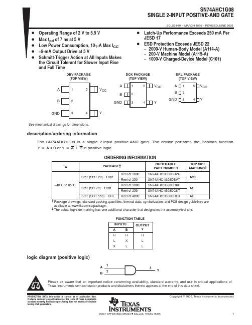
PINNING
PIN 1 2 3 4 5
SYMBOL inB inA GND outY VCC
DESCRIPTION data input B data input A ground (0 V) data output DC supply voltage
1998 Nov 10
2
Philips Semiconductors
4.13 4.32 − 5.63 5.81 −
3.7
−
5.2
−
VOL
LOW-level output
−
0
0.1
−
0.1
voltage; all outputs
−
0
0.1
−
0.1
−
0
0.1
−
74AHC1G08DBVRdatasheet
PACKAGING INFORMATION Orderable DeviceStatus (1)Package Type Package Drawing Pins Package Qty Eco Plan (2)Lead/Ball Finish MSL Peak Temp (3)SN74AHC1G08DBVRACTIVE SOT-23DBV 53000Green (RoHS &no Sb/Br)CU NIPDAU Level-1-260C-UNLIM SN74AHC1G08DBVRE4ACTIVE SOT-23DBV 53000Green (RoHS &no Sb/Br)CU NIPDAU Level-1-260C-UNLIM SN74AHC1G08DBVRG4ACTIVE SOT-23DBV 53000Green (RoHS &no Sb/Br)CU NIPDAU Level-1-260C-UNLIM SN74AHC1G08DBVTACTIVE SOT-23DBV 5250Green (RoHS &no Sb/Br)CU NIPDAU Level-1-260C-UNLIM SN74AHC1G08DBVTE4ACTIVE SOT-23DBV 5250Green (RoHS &no Sb/Br)CU NIPDAU Level-1-260C-UNLIM SN74AHC1G08DCKRACTIVE SC70DCK 53000Green (RoHS &no Sb/Br)CU NIPDAU Level-1-260C-UNLIM SN74AHC1G08DCKRE4ACTIVE SC70DCK 53000Green (RoHS &no Sb/Br)CU NIPDAU Level-1-260C-UNLIM SN74AHC1G08DCKRG4ACTIVE SC70DCK 53000Green (RoHS &no Sb/Br)CU NIPDAU Level-1-260C-UNLIM SN74AHC1G08DCKTACTIVE SC70DCK 5250Green (RoHS &no Sb/Br)CU NIPDAU Level-1-260C-UNLIM SN74AHC1G08DCKTE4ACTIVE SC70DCK 5250Green (RoHS &no Sb/Br)CU NIPDAU Level-1-260C-UNLIM SN74AHC1G08DRLRACTIVE SOP DRL 54000Green (RoHS &no Sb/Br)CU NIPDAU Level-1-260C-UNLIM SN74AHC1G08DRLRG4ACTIVE SOP DRL 54000Green (RoHS &no Sb/Br)CU NIPDAU Level-1-260C-UNLIM (1)The marketing status values are defined as follows:ACTIVE:Product device recommended for new designs.LIFEBUY:TI has announced that the device will be discontinued,and a lifetime-buy period is in effect.NRND:Not recommended for new designs.Device is in production to support existing customers,but TI does not recommend using this part in a new design.PREVIEW:Device has been announced but is not in production.Samples may or may not be available.OBSOLETE:TIhas discontinued the production of the device.(2)Eco Plan -The planned eco-friendly classification:Pb-Free (RoHS)or Green (RoHS &no Sb/Br)-please check /productcontent for the latest availability information and additional product content details.TBD:The Pb-Free/Green conversion plan has not been defined.Pb-Free (RoHS):TI's terms "Lead-Free"or "Pb-Free"mean semiconductor products that are compatible with the current RoHS requirements for all 6substances,including the requirement that lead not exceed 0.1%by weight in homogeneous materials.Where designed to be soldered at high temperatures,TI Pb-Free products are suitable for use in specified lead-free processes.Green (RoHS &no Sb/Br):TI defines "Green"to mean Pb-Free (RoHS compatible),and free of Bromine (Br)and Antimony (Sb)based flame retardants (Br or Sb do not exceed 0.1%by weight in homogeneous material)(3)MSL,Peak Temp.--The Moisture Sensitivity Level rating according to the JEDEC industry standard classifications,and peak solder temperature.Important Information and Disclaimer:The information provided on this page represents TI's knowledge and belief as of the date that it is provided.TI bases its knowledge and belief on information provided by third parties,and makes no representation or warranty as to the accuracy of such information.Efforts are underway to better integrate information from third parties.TI has taken and continues to take reasonable steps to provide representative and accurate information but may not have conducted destructive testing or chemical analysis on incoming materials and chemicals.TI and TI suppliers consider certain information to be proprietary,and thus CAS numbers and other limited information may not be available for release.In no event shall TI's liability arising out of such information exceed the total purchase price of the TI part(s)at issue in this document sold by TI to Customer on an annual basis.PACKAGE OPTION ADDENDUM 10-Oct-2005Addendum-Page 1IMPORTANT NOTICETexas Instruments Incorporated and its subsidiaries (TI) reserve the right to make corrections, modifications, enhancements, improvements, and other changes to its products and services at any time and to discontinue any product or service without notice. Customers should obtain the latest relevant information before placing orders and should verify that such information is current and complete. All products are sold subject to TI’s terms and conditions of sale supplied at the time of order acknowledgment.TI warrants performance of its hardware products to the specifications applicable at the time of sale in accordance with TI’s standard warranty. T esting and other quality control techniques are used to the extent TI deems necessary to support this warranty. Except where mandated by government requirements, testing of all parameters of each product is not necessarily performed.TI assumes no liability for applications assistance or customer product design. Customers are responsible for their products and applications using TI components. T o minimize the risks associated with customer products and applications, customers should provide adequate design and operating safeguards.TI does not warrant or represent that any license, either express or implied, is granted under any TI patent right, copyright, mask work right, or other TI intellectual property right relating to any combination, machine, or process in which TI products or services are used. Information published by TI regarding third-party products or services does not constitute a license from TI to use such products or services or a warranty or endorsement thereof. Use of such information may require a license from a third party under the patents or other intellectual property of the third party, or a license from TI under the patents or other intellectual property of TI.Reproduction of information in TI data books or data sheets is permissible only if reproduction is without alteration and is accompanied by all associated warranties, conditions, limitations, and notices. Reproduction of this information with alteration is an unfair and deceptive business practice. TI is not responsible or liable for such altered documentation.Resale of TI products or services with statements different from or beyond the parameters stated by TI for that product or service voids all express and any implied warranties for the associated TI product or service and is an unfair and deceptive business practice. TI is not responsible or liable for any such statements. Following are URLs where you can obtain information on other Texas Instruments products and application solutions:Products ApplicationsAmplifiers Audio /audioData Converters Automotive /automotiveDSP Broadband /broadbandInterface Digital Control /digitalcontrolLogic Military /militaryPower Mgmt Optical Networking /opticalnetwork Microcontrollers Security /securityTelephony /telephonyVideo & Imaging /videoWireless /wirelessMailing Address:Texas InstrumentsPost Office Box 655303 Dallas, Texas 75265Copyright 2005, Texas Instruments Incorporated。
74LVC1G08
74LVC1G08
SINGLE 2 INPUT POSITIVE AND GATE
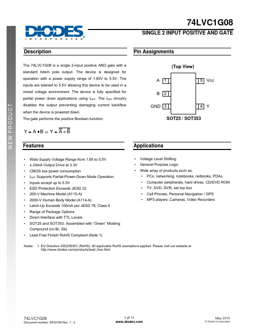
Description
Pin Assignments
The 74LVC1G08 is a single 2-input positive AND gate with a standard totem pole output. The device is designed for operation with a power supply range of 1.65V to 5.5V. The inputs are tolerant to 5.5V allowing this device to be used in a mixed voltage environment. The device is fully specified for partial power down applications using IOFF. The IOFF circuitry disables the output preventing damaging current backflow when the device is powered down. The gate performs the positive Boolean function:
Notes: 1. EU Directive 2002/95/EC (RoHS). All applicable RoHS exemptions applied. Please visit our website at /products/lead_free.html.
VCC = 1.65V
VCC = 2.3V
IOH
High-level output current VCC = 3V
RD74LVC1G08中文资料
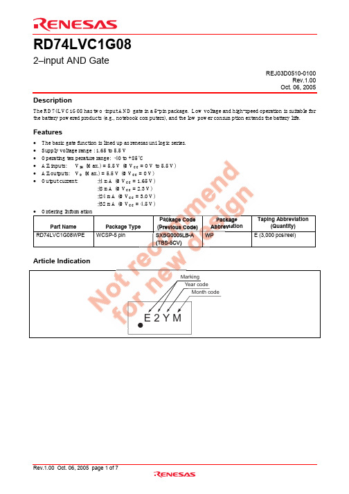
RD74LVC1G082–input AND GateREJ03D0510-0100Rev.1.00Oct. 06, 2005DescriptionThe RD74LVC1G08 has two–input AND gate in a 5-pin package. Low voltage and high-speed operation is suitable for the battery powered products (e.g., notebook computers), and the low power consumption extends the battery life.Features• The basic gate function is lined up as renesas uni logic series. • Supply voltage range : 1.65 to 5.5 V• Operating temperature range: –40 to +85°C• All inputs: V IH (Max.) = 5.5 V (@V CC = 0 V to 5.5 V) • All outputs: V O (Max.) = 5.5 V (@V CC = 0 V) • Output current: ±4 mA (@V CC = 1.65 V) ±8 mA (@V CC = 2.3 V) ±24 mA (@V CC = 3.0 V) ±32 mA (@V CC = 4.5 V) •Ordering InformationPart Name Package Type Package Code (Previous Code) Package Abbreviation Taping Abbreviation(Quantity) RD74LVC1G08WPEWCSP-5 pinE (3,000 pcs/reel)Article IndicationE 2 Y MMarking Year codeMonth codeAbbreviatio SXBG0005LB-A (TBS-5CV)WPMaPin Arrangement(Bottom view)(Top view)OUTY15234GNDHeight 0.4 mm 0.4 mm pitch0.17 mm 5–Ball (WP)0.7 mm1.1 m mINA INB VCCPin#1 INDEXLogic DiagramABFunction TableA B Output YL L H L L H L H HHH: High levelL: Low level(Top viYInputsL L HAbsolute Maximum RatingsItemSymbol Ratings Unit Test ConditionsSupply voltage range V CC –0.5 to 6.5 V Input voltage range *1 V I –0.5 to 6.5 V–0.5 to V CC +0.5 Output : H or L Output voltage range *1, 2 V O –0.5 to 6.5V V CC : OFF Input clamp current I IK –50 mA V I < 0 Output clamp currentI OK –50 mA V O < 0Continuous output current I O ±50 mA V O = 0 to V CC Continuous current through V CC or GNDI CC or I GND ±100 mA Package Thermal impedance θja 200 °C/W WP Storage temperature Tstg–65 to 150°CNotes: The absolute maximum ratings are values, which must not individually be exceeded, and furthermore no two of which may be realized at the same time.1. The input and output voltage ratings may be exceeded if the input and output clamp-current ratings areobserved.2. This value is limited to 5.5 V maximum.Recommended Operating ConditionsItemSymbol Min Max Unit Conditions Supply voltage range V CC 1.65Input voltage range V I 0 Output voltage range V O CC = 1.65 V V CC = 2.3 V V CC = 3.0 V I OLV CC = 4.5 V V CC = 1.65 V –8 V CC = 2.3 V –16 –24 V CC = 3.0 V Output current— –32 V CC = 4.5 V0 20 V CC = 1.65 to 1.95 V, 2.3 to 2.7 V 0 10 V CC = 3.0 to 3.6 V Input transition rise or fall rate 05 ns / VV CC = 4.5 to 5.5 V Operating free-air temperatureT a–4085°CNote: Unused or floating inputs must be held high or low.C5.5 V 5.5 V 0 V CC V— 8 — 16 — 24 — 32 — –4 — — — I OHmA— 4 V fall rate ∆t / ∆vTa = –40 to 85°CItemSymbol V CC (V)Min Typ Max UnitTest condition1.65 to 1.95V CC ×0.65 — — 2.3 to 2.7 1.7 — — 3.0 to 3.6 2.0 — — V IH 4.5 to 5.5V CC ×0.7 — — 1.65 to 1.95— — V CC ×0.352.3 to 2.7 — — 0.7 3.0 to 3.6 —— 0.8 Input voltageV IL 4.5 to 5.5— — V CC ×0.3VMin to MaxV CC –0.1 — — I OH = –100 µA 1.65 1.2 — — I OH = –4 mA 2.3 1.9 — — I OH = –8 mA 2.4 — — I OH = –16 mA 3.02.3 — — I OH = –24 mA V OH 4.53.8 — I OH = –32 mA Min to Max — — I OL = 100 µA 1.65 — — = 4 mA 2.3—— = 8 mA— — 0.4 I = 16 mA 3.0— OL = 24 mA Output voltage V OL4.5 — VI OL = 32 mAInput current I IN 0 to 5.5 µA V IN = 5.5 V or GNDI CC 5.5 V IN = V CC or GND, I O = 0 Quiescentsupply current∆I CC3 to 5.5µAOne input at V CC –0.6 V,Other input at V CC or GND Output leakagecurrentI OFF 0 ±10 µA V IN or V O = 0 to 5.5 VInput capacitance C IN — pF V IN = V CC or GND Note: For conditions shown as Min or Max, use the appropriate values under recommended operating conditions. — 0.1 0.45 I OL 0.3 I OL = 8 OL = 1— 0.55 I — 0.55 — — ±5 — — 10 ——500— — ±13.3 — 4.0 as Min or Max, use the appropriate vV CC = 1.8 ± 0.15 VTa = –40 to 85°C ItemSymbol Min Max Unit Test Conditions FROM(Input) TO (Output)1.5 7.2 C L = 15 pF, R L = 1 M ΩPropagation delay timet PLH t PHL2.48.0nsC L = 30 pF, R L = 1.0 k ΩA or BYV CC = 2.5 ± 0.2 VTa = –40 to 85°C ItemSymbol Min Max Unit Test Conditions FROM(Input) TO (Output)0.7 4.4 C L = 15 pF, R L = 1 M ΩPropagation delay timet PLH t PHL1.15.5nsC L = 30 pF, R L = 500 ΩA or BYV CC = 3.3 ± 0.3 VTa = –40 to 85°C ItemSymbol Min Max Unit Test Conditions FROM(Input) TO (Output)0.8 3.6 C L = 15 pF, R ΩPropagation delay timet PLH t PHL1.04.5nsC L A or BYV CC = 5.0 ± 0.5 VTa = –40 to 85°C ItemSymbol Min Max Unit Test Conditions FROM(Input) TO (Output)ΩPropagation delay timet PLH t PHL1.0nsL = 500 ΩA or BYOperating CharacteristicsTa = 25°C ItemMin Typ Max Unit Test Conditions 1.821 — — 24 — — 26 — Power dissipation capacitance —31—pFf = 10 MHzst Condit = 15 pF, R L = 1 M = 50 pF, R L = 500 ΩL = 15 pF, R L = 1 M 4.00.8 3.4 C C L = 50 pF, R Ta = 2Symbol V CC (V) — 2.5 —3.3 e CPD5.0Test CircuitLNote: C includes probe and jig capacitance.C L Measurement pointR L*From Output90%10%t PHLV CCGNDV OHV OLt rt f90%V ref V V refV ref 10%1.8±0.152.5±0.23.3±0.3 5.0±0.5I C L R L V CC V CC / 2V CC / 2V CC / 2Vref ≤ 2 ns ≤ 2 ns≤ 2.5 ns ≤ 2.5 ns V CCV CC 3 V 15 pF 1 M Ω1 M Ω1 M Ω1 M Ω15 pF 15 pF 15 pF1.5 V INPUTS t r / t f 1.8±0.152.5±0.23.3±0.35.0±0.5V I C L R L V CC V CC / 2V CC / 2V CC / 2Vref V CC (V)≤ 2 ns ≤ 2 ns≤ 2.5 ns ≤ 2.5 nsV CCV CC 3 V 30 pF 1.0 k Ω500 Ω500 Ω500 Ω30 pF 50 pF 50 pF1.5 V INPUTS t r / t f • WaveformsInputOutputNotes: 1. Input waveform: PRR ≤ 10 MHz, Zo = 50 Ω.2. The output are measured one at a time with one transition per measurement.t PLHrefV V CC (V)INPUPackage Dimensions*1.100.150.1400.110SXBG0005LB-AbZ e E AA D x y Z 1MASS[Typ.]0.150.05(0.235)0.150.19Reference SymbolDimension in Millimeters MinNomMax Previous Code JEITA Package Code S-XFBGA5-0.7x1.1-0.40RENESAS Code TBS-5CV0.001g0.402A 0.700.400.050.20ED eeDZ DZ EEA 1A 2ACBA12CA BSeating plane5 × φ b C φx M A B Cφx M y C*Reference value.Pin#1 index areaCy 1y1Keep safety first in your circuit designs!1. Renesas Technology Corp. puts the maximum effort into making semiconductor products better and more reliable, but there is always the possibility that trouble may occur with them. Trouble with semiconductors may lead to personal injury, fire or property damage.Remember to give due consideration to safety when making your circuit designs, with appropriate measures such as (i) placement of substitutive, auxiliary circuits, (ii) use of nonflammable material or (iii) prevention against any malfunction or mishap.Notes regarding these materials1. These materials are intended as a reference to assist our customers in the selection of the Renesas Technology Corp. product best suited to the customer's application; they do not convey any license under any intellectual property rights, or any other rights, belonging to Renesas Technology Corp. or a third party.2. Renesas Technology Corp. assumes no responsibility for any damage, or infringement of any third-party's rights, originating in the use of any product data,diagrams, charts, programs, algorithms, or circuit application examples contained in these materials.3. All information contained in these materials, including product data, diagrams, charts, programs and algorithms represents information on products at the time of publication of these materials, and are subject to change by Renesas Technology Corp. without notice due to product improvements or other reasons. It is therefore recommended that customers contact Renesas Technology Corp. or an authorized Renesas Technology Corp. product distributor for the latest product information before purchasing a product listed herein.The information described here may contain technical inaccuracies or typographical errors.Renesas Technology Corp. assumes no responsibility for any damage, liability, or other loss rising from these inaccuracies or errors. Please also pay attention to information published by Renesas Technology Corp. by various means, including the Renesas Technology Corp. Semiconductor home page ().4. When using any or all of the information contained in these materials, including product data, diagrams, charts, programs, and algorithms, please be sure to evaluate all information as a total system before making a final decision on the applicability of the information and products. Renesas Technology Corp. assumes no responsibility for any damage, liability or other loss resulting from the information contained herein.5. Renesas Technology Corp. semiconductors are not designed or manufactured for use in a device or system that is used under circumstances in which human life is potentially at stake. Please contact Renesas Technology Corp. or an authorized Renesas Technology Corp. product distributor when considering the use of a product contained herein for any specific purposes, such as apparatus or systems for transportation, vehicular, medical, aerospace, nuclear, or undersea repeater use.6. The prior written approval of Renesas Technology Corp. is necessary to reprint or reproduce in whole or in part these materials.7. If these products or technologies are subject to the Japanese export control restrictions, they must be exported under a license from the Japanese government and cannot be imported into a country other than the approved destination. Any diversion or reexport contrary to the export control laws and regulations of Japan and/or the country of destination is prohibited.8. Please contact Renesas Technology Corp. for further details on these materials or the products contained therein.Sales Strategic Planning Div. Nippon Bldg., 2-6-2, Ohte-machi, Chiyoda-ku, Tokyo 100-0004, JapanRefer to "/en/network " for the latest and detailed information.Renesas Technology America, Inc.450 Holger Way, San Jose, CA 95134-1368, U.S.A Tel: <1> (408) 382-7500, Fax: <1> (408) 382-7501Renesas Technology Europe Limited Dukes Meadow, Millboard Road, Bourne End, Buckinghamshire, SL8 5FH, U.K.Tel: <44> (1628) 585-100, Fax: <44> (1628) 585-900Renesas Technology Hong Kong Ltd. 7th Floor, North Tower, World Finance Centre, Harbour City, 1 Canton Road, Tsimshatsui, Kowloon, Hong Kong Tel: <852> 2265-6688, Fax: <852> 2730-6071Renesas Technology Taiwan Co., Ltd.10th Floor, No.99, Fushing North Road, Taipei, Taiwan Tel: <886> (2) 2715-2888, Fax: <886> (2) 2713-2999Renesas Technology (Shanghai) Co., Ltd.Unit2607 Ruijing Building, No.205 Maoming Road (S), Shanghai 200020, China Tel: <86> (21) 6472-1001, Fax: <86> (21) 6415-2952Renesas Technology Singapore Pte. Ltd.1 Harbour Front Avenue, #06-10, Keppel Bay Tower, Singapore 098632 Tel: <65> 6213-0200, Fax: <65> 6278-8001Renesas Technology Korea Co., Ltd.Kukje Center Bldg. 18th Fl., 191, 2-ka, Hangang-ro, Yongsan-ku, Seoul 140-702, Korea Tel: <82> 2-796-3115, Fax: <82> 2-796-2145Renesas Technology Malaysia Sdn. Bhd.Unit 906, Block B, Menara Amcorp, Amcorp Trade Centre, No.18, Jalan Persiaran Barat, 46050 Petaling Jaya, Selangor Darul Ehsan, Malaysia Tel: <603> 7955-9390, Fax: <603> 7955-9510RENESAS SALES OFFICES hnology Corp.longing to Renesaarty's rights, originating and algorithms represents infort notice due to product improvemenRenesas Technology Corp. product dis er loss rising from these inaccuracies or errors.various means, including the Renesas Technolog product data, diagrams, charts, programs, and algapplicability of the information and products. Ren rmation contained herein.ured for use in a device or system that is used unauthorized Renesas Technology Corp. product dis or systems for transportation, vehicular, medical,sary to reprint or reproduce in whole or in part thexport control restrictions, they must be exported u estination.s and regulations of Japan and/or the country of d etails on these materials or the products containem/en/network " for the latest and detailed infor ica, Inc.e, CA 95134-1368, U.S.A , Fax: <1> (408) 382-7501urope LimitedRoad, Bourne End, Buckinghamshire x: <44> (1628) 585-900g Ltd.ce Centre, Harbour 30-6071ES。
74ALVC08PW,118,74ALVC08BQ,115,74ALVC08BQ,115,74ALVC08BQ,115, 规格书,Datasheet 资料
74ALVC08
MAX. 3.6 3.6 VCC 3.6 +85 20 10 V V V V
UNIT
°C ns/V ns/V
LIMITING VALUES In accordance with the Absolute Maximum Rating System (IEC 60134); voltages are referenced to GND (ground = 0 V). SYMBOL VCC IIK VI IOK VO IO ICC, IGND Tstg Ptot Notes 1. The input and output voltage ratings may be exceeded if the input and output current ratings are observed. 2. When VCC = 0 V (Power-down mode), the output voltage can be 3.6 V in normal operation. 3. For SO14 packages: above 70 °C derate linearly with 8 mW/K. For TSSOP14 packages: above 60 °C derate linearly with 5.5 mW/K. For DHVQFN14 packages: above 60 °C derate linearly with 4.5 mW/K. PARAMETER supply voltage input diode current input voltage output diode current output voltage output source or sink current VCC or GND current storage temperature power dissipation Tamb = −40 to +85 °C; note 3 VO > VCC or VO < 0 notes 1 and 2 Power-down mode; note 2 VO = 0 to VCC VI < 0 CONDITIONS − −0.5 − −0.5 −0.5 − − −65 − MIN. −0.5 MAX. +4.6 −50 +4.6 ±50 +4.6 ±50 ±100 +150 500 V mA V mA V mA mA °C mW UNIT
74V1G08STR,74V1G08CTR,规格书,Datasheet 资料
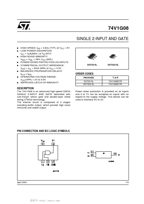
1/9April 2004s HIGH SPEED:t PD =3.8ns (TYP.)at V CC =5V sLOW POWER DISSIPATION:I CC =1µA(MAX.)at T A =25°C sHIGH NOISE IMMUNITY:V NIH =V NIL =28%V CC (MIN.)s POWER DOWN PROTECTION ON INPUTS sSYMMETRICAL OUTPUT IMPEDANCE:|I OH |=I OL =8mA (MIN)at V CC =4.5V sBALANCED PROPAGATION DELAYS:t PLH ≅t PHLsOPERATING VOLTAGE RANGE:V CC (OPR)=2V to 5.5VsIMPROVED LATCH-UP IMMUNITYDESCRIPTIONThe 74V1G08is an advanced high-speed CMOS SINGLE 2-INPUT AND GATE fabricated with sub-micron silicon gate and double-layer metal wiring C 2MOS technology.The internal circuit is composed of 2stages including buffer output,which provide high noise immunity and stable output.Power down protection is provided on all inputs and 0to 7V can be accepted on inputs with no regard to the supply voltage.This device can be used to interface 5V to 3V.74V1G08SINGLE 2-INPUT ANDGATEPIN CONNECTION AND IEC LOGIC SYMBOLSORDER CODESPACKAGE T &R SOT23-5L 74V1G08STR SOT323-5L74V1G08CTR74V1G082/9INPUT EQUIVALENT CIRCUITPIN DESCRIPTIONTRUTH TABLEABSOLUTE MAXIMUM RATINGSAbsolute Maximum Ratings are those values beyond which damage to the device may occur.Functional operation under these conditions is not implied.RECOMMENDED OPERATING CONDITIONS1)V IN from 30%to 70%of V CCPIN N°SYMBOL NAME AND FUNCTION 11A Data Input 21B Data Input 41Y Data Output 3GND Ground (0V)5V CCPositive Supply VoltageA B Y L L L L H L H L L HHHSymbol ParameterValue Unit V CC Supply Voltage -0.5to +7.0V V I DC Input Voltage -0.5to +7.0V V O DC Output Voltage -0.5to V CC +0.5V I IK DC Input Diode Current -20mA I OK DC Output Diode Current ±20mA I ODC Output Current±25mA I CC or I GND DC V CC or Ground Current±50mA T stg Storage Temperature-65to +150°C T LLead Temperature (10sec)260°CSymbol ParameterValue Unit V CC Supply Voltage 2to 5.5V V I Input Voltage 0to 5.5V V O Output Voltage 0to V CC V T op Operating Temperature-55to 125°C dt/dvInput Rise and Fall Time (note 1)(V CC =3.3±0.3V)(V CC =5.0±0.5V)0to 1000to 20ns/V ns/V74V1G083/9DC SPECIFICATIONSAC ELECTRICAL CHARACTERISTICS (Input t r =t f =3ns)(*)Voltage range is 3.3V ±0.3V (**)Voltage range is 5.0V ±0.5VCAPACITIVE CHARACTERISTICS1)C PD is defined as the value of the IC’s internal equivalent capacitance which is calculated from the operating current consumption without load.(Refer to Test Circuit).Average operating current can be obtained by the following equation.I CC(opr)=C PD x V CC x f IN +I CCSymbolParameterTest ConditionValue UnitV CC (V)T A =25°C -40to 85°C -55to 125°C Min.Typ.Max.Min.Max.Min.Max.V IHHigh Level Input Voltage 2.0 1.5 1.5 1.5V3.0to 5.50.7V CC0.7V CC0.7V CCV ILLow Level Input Voltage2.00.50.50.5V3.0to 5.50.3V CC0.3V CC0.3V CCV OHHigh Level Output Voltage2.0I O =-50µA 1.9 2.0 1.9 1.9V3.0I O =-50µA 2.9 3.0 2.9 2.94.5I O =-50µA 4.4 4.54.4 4.43.0I O =-4mA 2.58 2.48 2.44.5I O =-8mA 3.943.83.7V OLLow Level Output Voltage2.0I O =50µA 0.00.10.10.1V3.0I O =50µA 0.00.10.10.14.5I O =50µA 0.00.10.10.13.0I O =4mA 0.360.440.554.5I O =8mA 0.360.440.55I I Input Leakage Current0to 5.5V I =5.5V or GND ±0.1±1±1µA I CCQuiescent Supply Current5.5V I =V CC or GND11020µA SymbolParameterTest ConditionValueUnitV CC (V)C L (pF)T A =25°C -40to 85°C -55to 125°C Min.Typ.Max.Min.Max.Min.Max.t PLH t PHL Propagation DelayTime3.3(*)15 5.27.5 1.09.0 1.010.0ns 3.3(*)50 5.88.5 1.010.0 1.011.05.0(**)15 3.8 5.9 1.07.0 1.08.05.0(**)504.67.01.08.01.09.0SymbolParameterTest ConditionValue UnitT A =25°C -40to 85°C -55to 125°C Min.Typ.Max.Min.Max.Min.Max.C IN Input Capacitance 4101010pF C PDPower Dissipation Capacitance (note 1)10pF74V1G084/9TEST CIRCUITL R T =Z OUT of pulse generator (typically 50Ω)WAVEFORM:PROPAGATION DELAY (f=1MHz;50%dutycycle)74V1G087/974V1G08 Information furnished is believed to be accurate and reliable. However, STMicroelectronics assumes no responsibility for the consequences of use of such information nor for any infringement of patents or other rights of third parties which may result from its use. No license is granted by implication or otherwise under any patent or patent rights of STMicroelectronics. Specifications mentioned in this publication are subject to change without notice. This publication supersedes and replaces all information previously supplied. STMicroelectronics products are not authorized for use as critical components in life support devices or systems without express written approval of STMicroelectronics.The ST logo is a registered trademark of STMicroelectronicsAll other names are the property of their respective owners© 2004 STMicroelectronics - All Rights ReservedSTMicroelectronics GROUP OF COMPANIESAustralia - Belgium - Brazil - Canada - China - Czech Republic - Finland - France - Germany - Hong Kong - India - Israel - Italy - Japan - Malaysia - Malta - Morocco - Singapore - Spain - Sweden - Switzerland - United Kingdom - United States.9/9。
SN74LVC1G79YEPR,SN74LVC1G79YEPR,SN74LVC1G79DRLR,SN74LVC1G79DRLR, 规格书,Datasheet 资料

FEATURESSee mechanical drawings for dimensions.DBV PACKAGE (TOP VIEW)51V CCD 2CLK 34GNDQDRL PACKAGE (TOP VIEW)2CLK V CC 51D 34GNDQDCK PACKAGE (TOP VIEW)2CLK34GNDV CC5D Q1YZP PACKAGE (BOTTOMVIEW)CLK V CCGND Q DESCRIPTION/ORDERINGINFORMATIONSN74LVC1G79SINGLE POSITIVE-EDGE-TRIGGERED D-TYPE FLIP-FLOPSCES220S–APRIL 1999–REVISED NOVEMBER 2007•Available in the Texas Instruments NanoFree™•Latch-Up Performance Exceeds 100mA Per PackageJESD 78,Class II•Supports 5-V V CC Operation •ESD Protection Exceeds JESD 22•Inputs Accept Voltages to 5.5V –2000-V Human-Body Model (A114-A)•Max t pd of 4ns at 3.3V–200-V Machine Model (A115-A)•Low Power Consumption,10-µA Max I CC –1000-V Charged-Device Model (C101)•±24-mA Output Drive at 3.3V•I off Supports Partial-Power-Down Mode OperationThis single positive-edge-triggered D-type flip-flop is designed for 1.65-V to 5.5-V V CC operation.When data at the data (D)input meets the setup time requirement,the data is transferred to the Q output on the positive-going edge of the clock pulse.Clock triggering occurs at a voltage level and is not directly related to the rise time of the clock pulse.Following the hold-time interval,data at the D input can be changed without affecting the level at the output.NanoFree™package technology is a major breakthrough in IC packaging concepts,using the die as the package.This device is fully specified for partial-power-down applications using I off .The I off circuitry disables the outputs,preventing damaging current backflow through the device when it is powered down.Please be aware that an important notice concerning availability,standard warranty,and use in critical applications of Texas Instruments semiconductor products and disclaimers thereto appears at the end of this data sheet.NanoFree is a trademark of Texas Instruments.PRODUCTION DATA information is current as of publication date.Copyright ©1999–2007,Texas Instruments IncorporatedProducts conform to specifications per the terms of the Texas Instruments standard warranty.Production processing does not necessarily include testing of all parameters.CLKQSN74LVC1G79SINGLE POSITIVE-EDGE-TRIGGERED D-TYPE FLIP-FLOPSCES220S–APRIL 1999–REVISED NOVEMBER 2007ORDERING INFORMATIONT APACKAGE (1)(2)ORDERABLE PART NUMBER TOP-SIDE MARKING (3)NanoFree™–WCSP (DSBGA)0.23-mm Large Bump –YZP Reel of 3000SN74LVC1G79YZPR ___CR_(Pb-free)Reel of 3000SN74LVC1G79DBVR SOT (SOT-23)–DBV C79_–40°C to 85°CReel of 250SN74LVC1G79DBVT Reel of 3000SN74LVC1G79DCKR SOT (SC-70)–DCK CR_Reel of 250SN74LVC1G79DCKT SOT (DOT-553)–DRLReel of 4000SN74LVC1G79DRLRCR_(1)Package drawings,thermal data,and symbolization are available at /packaging .(2)For the most current package and ordering information,see the Package Option Addendum at the end of this document,or see the TI website at .(3)DBV/DCK/DRL:The actual top-side marking has one additional character that designates the assembly/test site.YZP:The actual top-side marking has three preceding characters to denote year,month,and sequence code,and one following character to designate the assembly/test site.Pin 1identifier indicates solder-bump composition (1=SnPb,•=Pb-free).FUNCTION TABLEINPUTS OUTPUTYCLK D ↑H H ↑L L LXQ 0LOGIC DIAGRAM (POSITIVE LOGIC)2Submit Documentation FeedbackCopyright ©1999–2007,Texas Instruments IncorporatedProduct Folder Link(s):SN74LVC1G79Absolute Maximum Ratings(1)SN74LVC1G79 SINGLE POSITIVE-EDGE-TRIGGERED D-TYPE FLIP-FLOPSCES220S–APRIL1999–REVISED NOVEMBER2007over operating free-air temperature range(unless otherwise noted)MIN MAX UNITV CC Supply voltage range–0.5 6.5VV I Input voltage range(2)–0.5 6.5VV O Voltage range applied to any output in the high-impedance or power-off state(2)–0.5 6.5VV O Voltage range applied to any output in the high or low state(2)(3)–0.5V CC+0.5VI IK Input clamp current V I<0–50mAI OK Output clamp current V O<0–50mAI O Continuous output current±50mAContinuous current through V CC or GND±100mADBV package206DCK package252θJA Package thermal impedance(4)°C/WDRL package142YZP package132T stg Storage temperature range–65150°C (1)Stresses beyond those listed under"absolute maximum ratings"may cause permanent damage to the device.These are stress ratingsonly,and functional operation of the device at these or any other conditions beyond those indicated under"recommended operating conditions"is not implied.Exposure to absolute-maximum-rated conditions for extended periods may affect device reliability.(2)The input negative-voltage and output voltage ratings may be exceeded if the input and output current ratings are observed.(3)The value of V CC is provided in the recommended operating conditions table.(4)The package thermal impedance is calculated in accordance with JESD51-7.Copyright©1999–2007,Texas Instruments Incorporated Submit Documentation Feedback3Product Folder Link(s):SN74LVC1G79Recommended Operating Conditions (1)SN74LVC1G79SINGLE POSITIVE-EDGE-TRIGGERED D-TYPE FLIP-FLOPSCES220S–APRIL 1999–REVISED NOVEMBER 2007MINMAX UNIT Operating1.65 5.5V CCSupply voltageVData retention only 1.5V CC =1.65V to 1.95V0.65×V CCV CC =2.3V to 2.7V 1.7V IHHigh-level input voltageVV CC =3V to 3.6V 2V CC =4.5V to 5.5V 0.7×V CCV CC =1.65V to 1.95V0.35×V CCV CC =2.3V to 2.7V 0.7V ILLow-level input voltageV V CC =3V to 3.6V 0.8V CC =4.5V to 5.5V0.3×V CCV I Input voltage 0 5.5V V OOutput voltage0V CC V V CC =1.65V –4V CC =2.3V–8I OHHigh-level output current–16mA V CC =3V –24V CC =4.5V –32V CC =1.65V 4V CC =2.3V8I OLLow-level output current16mA V CC =3V 24V CC =4.5V32V CC =1.8V ±0.15V,2.5V ±0.2V20Δt/Δv Input transition rise or fall rate V CC =3.3V ±0.3V 10ns/V V CC =5V ±0.5V5T A Operating free-air temperature–4085°C (1)All unused inputs of the device must be held at V CC or GND to ensure proper device operation.Refer to the TI application report,Implications of Slow or Floating CMOS Inputs ,literature number SCBA004.4Submit Documentation FeedbackCopyright ©1999–2007,Texas Instruments IncorporatedProduct Folder Link(s):SN74LVC1G79Electrical Characteristics Timing RequirementsSN74LVC1G79 SINGLE POSITIVE-EDGE-TRIGGERED D-TYPE FLIP-FLOPSCES220S–APRIL1999–REVISED NOVEMBER2007over recommended operating free-air temperature range(unless otherwise noted)PARAMETER TEST CONDITIONS V CC MIN TYP(1)MAX UNITI OH=–100µA 1.65V to5.5V V CC–0.1I OH=–4mA 1.65V 1.2I OH=–8mA 2.3V 1.9V OH VI OH=–16mA 2.43VI OH=–24mA 2.3I OH=–32mA 4.5V 3.8I OL=100µA 1.65V to5.5V0.1I OL=4mA 1.65V0.45I OL=8mA 2.3V0.3V OL VI OL=16mA0.43VI OL=24mA0.55I OL=32mA 4.5V0.55I I All inputs V I=5.5V or GND0to5.5V±10µAI off V I or V O=5.5V0±10µAI CC V I=5.5V or GND,I O=0 1.65V to5.5V10µAΔI CC One input at V CC–0.6V,Other inputs at V CC or GND3V to5.5V500µAC i V I=V CC or GND 3.3V4pF(1)All typical values are at V CC=3.3V,T A=25°C.over operating free-air temperature range(unless otherwise noted)(see Figure1)V CC=1.8V CC=2.5V CC=3.3V V CC=5V±0.15V±0.2V±0.3V±0.5VPARAMETER UNITMIN MAX MIN MAX MIN MAX MIN MAXf clock Clock frequency160160160160MHzt w Pulse duration,CLK high or low 2.5 2.5 2.5 2.5nsData high 2.2 1.4 1.3 1.2t su Setup time before CLK↑nsData low 2.6 1.4 1.3 1.2t h Hold time,data after CLK↑0.30.410.5nsCopyright©1999–2007,Texas Instruments Incorporated Submit Documentation Feedback5Product Folder Link(s):SN74LVC1G79Switching CharacteristicsSwitching CharacteristicsOperating CharacteristicsSN74LVC1G79SINGLE POSITIVE-EDGE-TRIGGERED D-TYPE FLIP-FLOPSCES220S–APRIL 1999–REVISED NOVEMBER 2007over recommended operating free-air temperature range,C L =15pF (unless otherwise noted)(see Figure 1)V CC =1.8V V CC =2.5V V CC =3.3V V CC =5V FROM TO ±0.15V ±0.2V ±0.3V ±0.5V PARAMETERUNIT(INPUT)(OUTPUT)MIN MAXMIN MAXMIN MAXMIN MAXf max 160160160160MHz t pdCLKQ2.59.1 1.26140.83.8ns over recommended operating free-air temperature range,C L =30pF or 50pF (unless otherwise noted)(see Figure 2)V CC =1.8V V CC =2.5V V CC =3.3V V CC =5V FROM TO ±0.15V ±0.2V ±0.3V ±0.5V PARAMETERUNIT(INPUT)(OUTPUT)MIN MAXMIN MAXMIN MAXMIN MAXf max 160160160160MHz t pdCLKQ3.99.927 1.7514.5ns T A =25°CV CC =1.8VV CC =2.5VV CC =3.3VV CC =5V TEST PARAMETERUNIT CONDITIONS TYP TYP TYP TYP C pdPower dissipation capacitancef =10MHz26262730pF6Submit Documentation FeedbackCopyright ©1999–2007,Texas Instruments IncorporatedProduct Folder Link(s):SN74LVC1G79PARAMETER MEASUREMENT INFORMATIONFrom OutputUnder Test(see NoteLOAD CIRCUITVOpenData InputTiming Input0 V0 V0 VInput0 VInputOutputWaveform 1S1 at V(see Note B)LOADOutputWaveform 2S1 at GND(see Note B)VOLVOH0 V»0 V OutputOutputt/tPLH PHLOpenTEST S1OutputControl1.8 V0.15 V±2.5 V0.2 V±3.3 V0.3 V±5 V0.5 V±1 M W1 M W1 M W1 M WVCCRL2 ×VCC2 ×VCC6 V2 ×VCCVLOADCL15 pF15 pF15 pF15 pF0.15 V0.15 V0.3 V0.3 VVD3 VVIVCC/2VCC/21.5 VVCC/2VM£2 ns£2 ns£2.5 ns£2.5 nsINPUTSt/tr fVCCVCCVCCVLOADt/tPLZ PZLGNDt/tPHZ PZHVOLTAGE WAVEFORMSENABLE AND DISABLE TIMESLOW-AND HIGH-LEVEL ENABLINGVOLTAGE WAVEFORMSPROPAGATION DELAY TIMESINVERTING AND NONINVERTING OUTPUTSNOTES: A.C includes probe and jig capacitance.B.Waveform 1 is for an output with internal conditions such that the output is low, except when disabled by the output control.Waveform 2 is for an output with internal conditions such that the output is high, except when disabled by the output control.C.All input pulses are supplied by generators having the following characteristics: PRR10 MHz, Z= 50.D.The outputs are measured one at a time, with one transition per measurement.E.t and t are the same as t.F.t and t are the same as t.G.t and t are the same as t.H.All parameters and waveforms are not applicable to all devices.LOPLZ PHZ disPZL PZH enPLH PHL pd£WVOLTAGE WAVEFORMSPULSE DURATIONVOLTAGE WAVEFORMSSETUP AND HOLD TIMESVIVIVIV/2LOADVOLVOHVIVIVOHVOLSN74LVC1G79SINGLE POSITIVE-EDGE-TRIGGERED D-TYPE FLIP-FLOPSCES220S–APRIL1999–REVISED NOVEMBER2007Figure1.Load Circuit and Voltage WaveformsCopyright©1999–2007,Texas Instruments Incorporated Submit Documentation Feedback7Product Folder Link(s):SN74LVC1G79From OutputUnder Test(see NoteLOAD CIRCUITOpenData InputTiming Input0 V0 V0 VInput0 VInputOutputWaveform 1S1 at V(see Note B)LOADOutputWaveform 2S1 at GND(see Note B)VOLVOH0 V»0 V OutputOutputTEST S1t/tPLH PHLOpenOutputControl1.8 V0.15 V±2.5 V0.2 V±3.3 V0.3 V±5 V0.5 V±1 k W500W500W500WVCCRL2 ×VCC2 ×VCC6 V2 ×VCCVLOADCL30 pF30 pF50 pF50 pF0.15 V0.15 V0.3 V0.3 VVD3 VVIVCC/2VCC/21.5 VVCC/2VM£2 ns£2 ns£2.5 ns£2.5 nsINPUTSt/tr fVCCVCCVCCVLOADt/tPLZ PZLGNDt/tPHZ PZHVOLTAGE WAVEFORMSENABLE AND DISABLE TIMESLOW-AND HIGH-LEVEL ENABLINGVOLTAGE WAVEFORMSPROPAGATION DELAY TIMESINVERTING AND NONINVERTING OUTPUTSNOTES: A.C includes probe and jig capacitance.B.Waveform 1 is for an output with internal conditions such that the output is low, except when disabled by the output control.Waveform 2 is for an output with internal conditions such that the output is high, except when disabled by the output control.C.All input pulses are supplied by generators having the following characteristics: PRR10 MHz, Z= 50.D.The outputs are measured one at a time, with one transition per measurement.E.t and t are the same as t.F.t and t are the same as t.G.t and t are the same as t.H.All parameters and waveforms are not applicable to all devices.LOPLZ PHZ disPZL PZH enPLH PHL pd£WVOLTAGE WAVEFORMSPULSE DURATIONVOLTAGE WAVEFORMSSETUP AND HOLD TIMESVIVIVIV/2LOADVOLVOHVIVIVOHVOLSN74LVC1G79SINGLE POSITIVE-EDGE-TRIGGERED D-TYPE FLIP-FLOPSCES220S–APRIL1999–REVISED NOVEMBER2007PARAMETER MEASUREMENT INFORMATION(continued)Figure2.Load Circuit and Voltage Waveforms8Submit Documentation Feedback Copyright©1999–2007,Texas Instruments IncorporatedProduct Folder Link(s):SN74LVC1G79PACKAGING INFORMATIONOrderable Device Status(1)PackageType PackageDrawingPins PackageQtyEco Plan(2)Lead/Ball Finish MSL Peak Temp(3)SN74LVC1G79DBVR ACTIVE SOT-23DBV53000Green(RoHS&no Sb/Br)CU NIPDAU Level-1-260C-UNLIMSN74LVC1G79DBVRE4ACTIVE SOT-23DBV53000Green(RoHS&no Sb/Br)CU NIPDAU Level-1-260C-UNLIMSN74LVC1G79DBVRG4ACTIVE SOT-23DBV53000Green(RoHS&no Sb/Br)CU NIPDAU Level-1-260C-UNLIMSN74LVC1G79DBVT ACTIVE SOT-23DBV5250Green(RoHS&no Sb/Br)CU NIPDAU Level-1-260C-UNLIMSN74LVC1G79DBVTE4ACTIVE SOT-23DBV5250Green(RoHS&no Sb/Br)CU NIPDAU Level-1-260C-UNLIMSN74LVC1G79DBVTG4ACTIVE SOT-23DBV5250Green(RoHS&no Sb/Br)CU NIPDAU Level-1-260C-UNLIMSN74LVC1G79DCKR ACTIVE SC70DCK53000Green(RoHS&no Sb/Br)CU NIPDAU Level-1-260C-UNLIMSN74LVC1G79DCKRE4ACTIVE SC70DCK53000Green(RoHS&no Sb/Br)CU NIPDAU Level-1-260C-UNLIMSN74LVC1G79DCKRG4ACTIVE SC70DCK53000Green(RoHS&no Sb/Br)CU NIPDAU Level-1-260C-UNLIMSN74LVC1G79DCKT ACTIVE SC70DCK5250Green(RoHS&no Sb/Br)CU NIPDAU Level-1-260C-UNLIMSN74LVC1G79DCKTE4ACTIVE SC70DCK5250Green(RoHS&no Sb/Br)CU NIPDAU Level-1-260C-UNLIMSN74LVC1G79DCKTG4ACTIVE SC70DCK5250Green(RoHS&no Sb/Br)CU NIPDAU Level-1-260C-UNLIMSN74LVC1G79DRLR ACTIVE SOT DRL54000Green(RoHS&no Sb/Br)CU NIPDAU Level-1-260C-UNLIMSN74LVC1G79DRLRG4ACTIVE SOT DRL54000Green(RoHS&no Sb/Br)CU NIPDAU Level-1-260C-UNLIMSN74LVC1G79YZPR ACTIVE DSBGA YZP53000Green(RoHS&no Sb/Br)SNAGCU Level-1-260C-UNLIM(1)The marketing status values are defined as follows:ACTIVE:Product device recommended for new designs.LIFEBUY:TI has announced that the device will be discontinued,and a lifetime-buy period is in effect.NRND:Not recommended for new designs.Device is in production to support existing customers,but TI does not recommend using this part in a new design.PREVIEW:Device has been announced but is not in production.Samples may or may not be available.OBSOLETE:TI has discontinued the production of the device.(2)Eco Plan-The planned eco-friendly classification:Pb-Free(RoHS),Pb-Free(RoHS Exempt),or Green(RoHS&no Sb/Br)-please check /productcontent for the latest availability information and additional product content details.TBD:The Pb-Free/Green conversion plan has not been defined.Pb-Free(RoHS):TI's terms"Lead-Free"or"Pb-Free"mean semiconductor products that are compatible with the current RoHS requirements for all6substances,including the requirement that lead not exceed0.1%by weight in homogeneous materials.Where designed to be soldered at high temperatures,TI Pb-Free products are suitable for use in specified lead-free processes.Pb-Free(RoHS Exempt):This component has a RoHS exemption for either1)lead-based flip-chip solder bumps used between the die and package,or2)lead-based die adhesive used between the die and leadframe.The component is otherwise considered Pb-Free(RoHS compatible)as defined above.Green(RoHS&no Sb/Br):TI defines"Green"to mean Pb-Free(RoHS compatible),and free of Bromine(Br)and Antimony(Sb)based flame retardants(Br or Sb do not exceed0.1%by weight in homogeneous material)(3)MSL,Peak Temp.--The Moisture Sensitivity Level rating according to the JEDEC industry standard classifications,and peak solder temperature.Important Information and Disclaimer:The information provided on this page represents TI's knowledge and belief as of the date that it is provided.TI bases its knowledge and belief on information provided by third parties,and makes no representation or warranty as to the accuracy of such information.Efforts are underway to better integrate information from third parties.TI has taken and continues to take reasonable steps to provide representative and accurate information but may not have conducted destructive testing or chemical analysis on incoming materials and chemicals.TI and TI suppliers consider certain information to be proprietary,and thus CAS numbers and other limited information may not be available for release.In no event shall TI's liability arising out of such information exceed the total purchase price of the TI part(s)at issue in this document sold by TI to Customer on an annual basis.OTHER QUALIFIED VERSIONS OF SN74LVC1G79:•Enhanced Product:SN74LVC1G79-EPNOTE:Qualified Version Definitions:•Enhanced Product-Supports Defense,Aerospace and Medical ApplicationsTAPE AND REEL INFORMATION*All dimensions are nominalDevicePackage Type Package Drawing Pins SPQReel Diameter (mm)Reel Width W1(mm)A0(mm)B0(mm)K0(mm)P1(mm)W (mm)Pin1Quadrant SN74LVC1G79DBVR SOT-23DBV 53000178.09.2 3.3 3.2 1.55 4.08.0Q3SN74LVC1G79DBVR SOT-23DBV 53000178.09.0 3.23 3.17 1.37 4.08.0Q3SN74LVC1G79DBVT SOT-23DBV 5250178.09.2 3.3 3.2 1.55 4.08.0Q3SN74LVC1G79DBVT SOT-23DBV 5250178.09.0 3.23 3.17 1.37 4.08.0Q3SN74LVC1G79DCKR SC70DCK 53000178.09.0 2.4 2.5 1.2 4.08.0Q3SN74LVC1G79DCKR SC70DCK 53000178.09.2 2.4 2.4 1.22 4.08.0Q3SN74LVC1G79DCKT SC70DCK 5250178.09.0 2.4 2.5 1.2 4.08.0Q3SN74LVC1G79DCKT SC70DCK 5250178.09.2 2.4 2.4 1.22 4.08.0Q3SN74LVC1G79DRLR SOT DRL 54000180.09.5 1.78 1.780.69 4.08.0Q3SN74LVC1G79DRLR SOT DRL 54000180.08.4 1.98 1.780.69 4.08.0Q3SN74LVC1G79YZPRDSBGAYZP53000178.09.21.021.520.634.08.0Q1*All dimensions are nominalDevice Package Type Package Drawing Pins SPQ Length(mm)Width(mm)Height(mm) SN74LVC1G79DBVR SOT-23DBV53000180.0180.018.0 SN74LVC1G79DBVR SOT-23DBV53000180.0180.018.0 SN74LVC1G79DBVT SOT-23DBV5250180.0180.018.0 SN74LVC1G79DBVT SOT-23DBV5250180.0180.018.0 SN74LVC1G79DCKR SC70DCK53000180.0180.018.0 SN74LVC1G79DCKR SC70DCK53000180.0180.018.0 SN74LVC1G79DCKT SC70DCK5250180.0180.018.0 SN74LVC1G79DCKT SC70DCK5250180.0180.018.0 SN74LVC1G79DRLR SOT DRL54000180.0180.030.0 SN74LVC1G79DRLR SOT DRL54000202.0201.028.0SN74LVC1G79YZPR DSBGA YZP53000220.0220.035.0IMPORTANT NOTICETexas Instruments and its subsidiaries (TI) reserve the right to make changes to their products or to discontinue any product or service without notice, and advise customers to obtain the latest version of relevant information to verify, before placing orders, that information being relied on is current and complete. All products are sold subject to the terms and conditions of sale supplied at the time of order acknowledgement, including those pertaining to warranty, patent infringement, and limitation of liability.TI warrants performance of its semiconductor products to the specifications applicable at the time of sale in accordance with TI’s standard warranty. Testing and other quality control techniques are utilized to the extent TI deems necessary to support this warranty. Specific testing of all parameters of each device is not necessarily performed, except those mandated by government requirements.CERTAIN APPLICATIONS USING SEMICONDUCTOR PRODUCTS MAY INVOLVE POTENTIAL RISKS OF DEATH, PERSONAL INJURY, OR SEVERE PROPERTY OR ENVIRONMENTAL DAMAGE (“CRITICAL APPLICATIONS”). TI SEMICONDUCTOR PRODUCTS ARE NOT DESIGNED, AUTHORIZED, OR WARRANTED TO BE SUITABLE FOR USE IN LIFE-SUPPORT DEVICES OR SYSTEMS OR OTHER CRITICAL APPLICATIONS. INCLUSION OF TI PRODUCTS IN SUCH APPLICATIONS IS UNDERSTOOD TO BE FULLY AT THE CUSTOMER’S RISK.In order to minimize risks associated with the customer’s applications, adequate design and operating safeguards must be provided by the customer to minimize inherent or procedural hazards.TI assumes no liability for applications assistance or customer product design. TI does not warrant or represent that any license, either express or implied, is granted under any patent right, copyright, mask work right, or other intellectual property right of TI covering or relating to any combination, machine, or process in which such semiconductor products or services might be or are used. TI’s publication of information regarding any third party’s products or services does not constitute TI’s approval, warranty or endorsement thereof.Copyright © 1998, Texas Instruments Incorporated。
74LVC1G74DC-G中文资料

2 of 20
NXP Semiconductors
74LVC1G74
Single D-type flip-flop with set and reset; positive edge trigger
C
C C
D
C RD
SD
CP
C
C
Fig 3. Logic diagram
6. Pinning information
plastic extremely thin small outline package; no leads; SOT996-2 8 terminals; UTLP based; body 3 × 2 × 0.5 mm
plastic extremely thin quad flat package; no leads; 8 terminals; UTLP based; body 1.6 × 1.6 × 0.5 mm
SN74LVC1G57DBVR,SN74LVC1G57DBVR,SN74LVC1G57DBVR,SN74LVC1G57DCKR, 规格书,Datasheet 资料

Reel of 3000 SN74LVC1G57DBVR
SOT (SC-70) – DCK
Reel of 3000 SN74LVC1G57DCKR
SOT (SOT-563) – DRL QFN – DRY(3) µf 4000 Reel of 5000 Reel of 5000
Submit Documentation Feedback
3
SN74LVC1G57
SCES414M – NOVEMBER 2002 – REVISED OCTOBER 2011
Absolute Maximum Ratings(1)
over operating free-air temperature range (unless otherwise noted)
SN74LVC1G57DRLR SN74LVC1G57DRYR SN74LVC1G57DSFR
TOP-SIDE MARKING(2)
_ _ _CL_
CA7_ CL_ CL_ CL CL
(1) Package drawings, standard packing quantities, thermal data, symbolization, and PCB design guidelines are available at /sc/package.
74HC1G08数据手册

1.5 3.15 4.2
-
1.9 4.4 5.9 3.7 5.2
-
-
0.5 1.35 1.8
-
0.1 0.1 0.1 0.4 0.4 1.0 20
-
VIH
HIGH-level input
VCC = 4.5 V to 5.5 V
voltage
2.0 1.6
-
2.0
-
VIL
LOW-level input
3. Ordering information
Table 1. Ordering information
Type number
Package
Temperature range Name
74HC1G08GW
−40 °C to +125 °C TSSOP5
74HCT1G08GW
74HC1G08GV
−40 °C to +125 °C SC-74A
2-input AND gate
1B 2A
Fig 1. Logic symbol
Y4 mna113
1
&
4
2
mna114
Fig 2. IEC logic symbol
B A
Fig 3. Logic diagram
Y
mna115
6. Pinning information
6.1 Pinning
74HC1G08 74HCT1G08
2.0
5.0
6.0
0
-
VCC
0
-
VCC
−40 +25 +125
-
-
625
-
74LVC1G86GW中文资料

74LVC1G86
Tamb (°C) −40 to +85 TYP.(1) − − − − 0.7 0.8 0.3 × VCC 0.1 0.45 0.3 0.4 0.55 0.55 − − − − − − ±5 ±10 10 − − − − − − − − − − − − − − − − − − − ±0.1 ±0.1 0.1 MAX. V V V V V V V V V V V V V V V V V V V µA µA µA UNIT
1.65 to 5.5 1.65 2.3 2.7 3.0 4.5 1.65 2.3 2.7 3.0 4.5 3.6 0 5.5
VOH
HIGH-level output voltage
VI = VIH or VIL; IO = −100 µA 1.65 to 5.5 VI = VIH or VIL; IO = −4 mA VI = VIH or VIL; IO = −8 mA VI = VIH or VIL; IO = −12 mA VI = VIH or VIL; IO = −24 mA VI = VIH or VIL; IO = −32 mA
LIMITING VALUES In accordance with the Absolute Maximum Rating System (IEC 60134); voltages are referenced to GND (ground = 0 V). SYMBOL VCC IIK VI IOK VO IO ICC, IGND Tstg PD Notes 1. The input and output voltage ratings may be exceeded if the input and output current ratings are observed. 2. When VCC = 0 V (Power-down mode), the output voltage can be 5.5 V in normal operation. 3. Above 55 °C the value of PD derates linearly with 2.5 mW/K. 2001 Apr 06 4 PARAMETER supply voltage input diode current input voltage output diode current output voltage output source or sink current VCC or GND current storage temperature power dissipation per package for temperature range from −40 to +85 °C; note 3 VI < 0 note 1 VO > VCC or VO < 0 active mode; notes 1 and 2 VO = 0 to VCC CONDITIONS − −0.5 − −0.5 − − −65 − MIN. −0.5 MAX. +6.5 −50 +6.5 ±50 VCC + 0.5 +6.5 ±50 ±100 +150 200 V mA V mA V V mA mA °C mW UNIT
74LCX08SJ中文资料

© 2005 Fairchild Semiconductor Corporation DS012411March 1995Revised February 200574LCX08 Low Voltage Quad 2-Input AND Gate with 5V Tolerant Inputs74LCX08Low Voltage Quad 2-Input AND Gate with 5V Tolerant InputsGeneral DescriptionThe LCX08 contains four 2-input AND gates. The inputs tolerate voltages up to 7V allowing the interface of 5V sys-tems to 3V systems.The 74LVX08 is fabricated with advanced CMOS technol-ogy to achieve high speed operation while maintaining CMOS low power dissipation.Featuress 5V tolerant inputss 2.3V–3.6V V CC specifications provided s 5.5 ns t PD max (V CC 3.3V), 10 P A I CC max s Power down high impedance inputs and outputs s r 24 mA output drive (V CC 3.0V)s Implements patented noise/EMI reduction circuitry s Latch-up performance exceeds JEDEC 78 conditions s ESD performance:Human body model ! 2000V Machine model ! 150V s Leadless Pb-Free DQFN packageOrdering Code:Devices also available in T ape and Reel. Specify by appending the suffix letter “X ” to the ordering code.Pb-Free package per JEDEC J-STD-020B.Note 1: “_NL ” indicates Pb-Free product (per JEDEC J-STD-020B). Device is available in Tape and Reel only.Note 2: DQFN package available in Tape and Reel only.Order Number Package Number Package Description74LCX08M M14A 14-Lead Small Outline Integrated Circuit (SOIC), JEDEC MS-012, 0.150" Narrow 74LCX08MX_NL (Note 1)M14A Pb-Free 14-Lead Small Outline Integrated Circuit (SOIC), JEDEC MS-012, 0.150" Narrow 74LCX08SJ M14D Pb-Free 14-Lead Small Outline Package (SOP), EIAJ TYPE II, 5.3mm Wide74LCX08BQX (Note 2)MLP014A Pb-Free 14-Terminal Depopulated Quad Very-Thin Flat Pack No Leads (DQFN), JEDEC MO-241, 2.5 x 3.0mm74LCX08MTC MTC1414-Lead Thin Shrink Small Outline Package (TSSOP), JEDEC MO-153, 4.4mm Wide 74LCX08MTCX_NL (Note 1)MTC14Pb-Free 14-Lead Thin Shrink Small Outline Package (TSSOP), JEDEC MO-153, 4.4mm Wide 274L C X 08Logic SymbolIEEE/IECPin DescriptionsConnection DiagramsPin Assignments for SOIC, SOP , and TSSOPPad Assignments for DQFN(Top View)Pin Names Description A n , B n Inputs O nOutputs74LCX08Absolute Maximum Ratings (Note 3)Recommended Operating Conditions (Note 5)Note 3: The Absolute Maximum Ratings are those values beyond which the safety of the device cannot be guaranteed. The device should not be operated at these limits. The parametric values defined in the Electrical Characteristics tables are not guaranteed at the Absolute Maximum Ratings. The “Recom-mended Operating Conditions ” table will define the conditions for actual device operation.Note 4: I O Absolute Maximum Rating must be observed.Note 5: Unused inputs must be held HIGH or LOW. They may not float.DC Electrical CharacteristicsSymbol ParameterValueConditionsUnits V CC Supply Voltage 0.5 to 7.0V V I DC Input Voltage 0.5 to 7.0VV O DC Output Voltage 0.5 to V CC 0.5Output in HIGH or LOW State (Note 4)V I IK DC Input Diode Current 50V I GND mA I OK DC Output Diode Current 50V O GND mA 50V O ! V CCI O DC Output Source/Sink Current r 50mA I CC DC Supply Current per Supply Pin r 100mA I GND DC Ground Current per Ground Pin r 100mAT STGStorage Temperature65 to 150q CSymbol ParameterMin Max Units V CC Supply Voltage Operating 2.0 3.6V Data Retention1.5 3.6V I Input Voltage 0 5.5V V O Output Voltage HIGH or LOW State 0V CCV I OH /I OLOutput CurrentV CC 3.0V 3.6V r 24mAV CC 2.7V 3.0V r 12V CC 2.3V 2.7Vr 8T AFree-Air Operating Temperature4085q C 't/'VInput Edge Rate, V IN 0.8V –2.0V, V CC 3.0V10ns/VSymbol ParameterConditionsV CC T A 40q C to 85q C Units (V)Min MaxV IH HIGH Level Input Voltage 2.3 2.7 1.7V 2.7 3.6 2.0V IL LOW Level Input Voltage 2.3 2.70.7V2.33.60.8V OHHIGH Level Output VoltageI OH 100 P A 2.3 3.6V CC 0.2VI OH = -8 mA 2.3 1.8I OH 12 mA 2.7 2.2I OH 18 mA 3.0 2.4I OH 24 mA3.0 2.2V OLLOW Level Output VoltageI OL 100 P A 2.3 3.60.2V I OL = 8mA 2.30.6I OL 12 mA 2.70.4I OL 16 mA 3.00.4I OL 24 mA3.00.55I I Input Leakage Current 0 d V I d 5.5V 2.3 3.6r 5.0P A I OFF Power-Off Leakage Current V I or V O 5.5V 010P A I CC Quiescent Supply Current V I V CC or GND 2.3 3.610P A 3.6V d V I d 5.5V 2.3 3.6r 10'I CCIncrease in I CC per InputV IH V CC 0.6V2.33.6500P A 474L C X 08AC Electrical CharacteristicsNote 6: Skew is defined as the absolute value of the difference between the actual propagation delay for any two separate outputs of the same device. The specification applies to any outputs switching in the same direction, either HIGH-to-LOW (t OSHL ) or LOW-to-HIGH (t OSLH ).Dynamic Switching CharacteristicsCapacitanceSymbolParameterT A 40q C to 85q C, R L 500:UnitsV CC 3.3V r 0.3VV CC 2.7V V CC 2.5V r 0.2VC L 50 pF C L 50 pF C L 30 pF MinMax Min Max Min Max t PHL Propagation Delay1.5 5.5 1.5 6.2 1.5 6.6ns t PLH 1.55.5 1.56.21.56.6t OSHL Output to Output Skew (Note 6) 1.0ns t OSLH1.0Symbol ParameterConditionsV CC T A 25q C Units (V)Typical V OLP Quiet Output Dynamic Peak V OL C L 50 pF, V IH 3.3V, V IL 0V 3.30.8V C L 30 pF, V IH 2.5V, V IL 0V 2.50.6V OLVQuiet Output Dynamic Valley V OLC L 50 pF, V IH 3.3V, V IL 0V 3.3 0.8VC L 30 pF, V IH 2.5V, V IL 0V2.50.6Symbol ParameterConditionsTypical Units C IN Input Capacitance V CC Open, V I 0V or V CC 7pF C OUT Output CapacitanceV CC 3.3V, V I 0V or V CC8pF C PDPower Dissipation CapacitanceV CC 3.3V, V I 0V or V CC , f 10 MHz25pF74LCX08AC Loading and Waveforms Generic for LCX FamilyFIGURE 1. AC Test Circuit(C L includes probe and jig capacitance)Waveform for Inverting and Non-Inverting FunctionsPropagation Delay, Pulse Width and t rec Waveforms3-STATE Output High Enable andDisable TImes for Logic3-STATE Output Low Enable andDisable Times for LogicSetup Time, Hold TIme and Recovery TIme for Logict rise and t fallFIGURE 2. Waveforms(Input Pulse Characteristics; f = 1MHz, t r = t f = 3ns)Test Switcht PLH, t PHL Opent PZL, t PLZ6V at V CC 3.3 r 0.3VV CC x 2 at V CC 2.5 r 0.2Vt PZH,t PHZ GNDSymbolV CC3.3V r 0.3V 2.7V 2.5V r 0.2VV mi 1.5V 1.5V V CC/2V mo 1.5V 1.5V V CC/2V x V OL 0.3V V OL 0.3V V OL 0.15VV y V OH 0.3V V OH 0.3V V OH 0.15V 674L C X 08Schematic DiagramGeneric for LCX Family74LCX08Tape and Reel SpecificationTape Format for DQFNTAPE DIMENSIONS inches (millimeters)REEL DIMENSIONS inches (millimeters)PackageTape Number Cavity Cover Tape DesignatorSection Cavities Status Status Leader (Start End)125 (typ)Empty Sealed BQXCarrier 3000Filled Sealed Trailer (Hub End)75 (typ)EmptySealedTapeSize A B C D N W1W212 mm13.00.0590.5120.795 2.1650.4880.724(330.0)(1.50)(13.00)(20.20)(55.00)(12.4)(18.4) 874L C X 08Physical Dimensionsinches (millimeters) unless otherwise noted14-Lead Small Outline Integrated Circuit (SOIC), JEDEC MS-012, 0.150" NarrowPackage Number M14A 74LCX08Physical Dimensions inches (millimeters) unless otherwise noted (Continued)Pb-Free 14-Lead Small Outline Package (SOP), EIAJ TYPE II, 5.3mm WidePackage Number M14D 1074L C X 08Physical Dimensionsinches (millimeters) unless otherwise noted (Continued)Pb-Free 14-Terminal Depopulated Quad Very-Thin Flat Pack No Leads (DQFN), JEDEC MO-241, 2.5 x 3.0mmPackage Number MLP014APhysical Dimensions inches (millimeters) unless otherwise noted (Continued)14-Lead Thin Shrink Small Outline Package (TSSOP), JEDEC MO-153, 4.4mm WidePackage Number MTC14Fairchild does not assume any responsibility for use of any circuitry described, no circuit patent licenses are implied and Fairchild reserves the right at any time without notice to change said circuitry and specifications.LIFE SUPPORT POLICYFAIRCHILD’S PRODUCTS ARE NOT AUTHORIZED FOR USE AS CRITICAL COMPONENTS IN LIFE SUPPORT DEVICES OR SYSTEMS WITHOUT THE EXPRESS WRITTEN APPROVAL OF THE PRESIDENT OF FAIRCHILD SEMICONDUCTOR CORPORATION. As used herein:1.Life support devices or systems are devices or systemswhich, (a) are intended for surgical implant into the body, or (b) support or sustain life, and (c) whose failure to perform when properly used in accordance with instructions for use provided in the labeling, can be rea-sonably expected to result in a significant injury to the user.2. A critical component in any component of a life supportdevice or system whose failure to perform can be rea-sonably expected to cause the failure of the life support device or system, or to affect its safety or effectiveness.元器件交易网 74LCX08 Low Voltage Quad 2-Input AND Gate with 5V Tolerant Inputs。
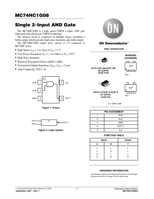
MC74HC1G00DTT1G, 规格书,Datasheet 资料

MC74HC1G00Single 2-Input NAND GateThe MC74HC1G00 is a high speed CMOS 2−input NAND gate fabricated with silicon gate CMOS technology.The internal circuit is composed of multiple stages, including a buffer output which provides high noise immunity and stable output.•High Speed: t PD = 7 ns (Typ) at V CC = 5 V•Low Power Dissipation: I CC = 1 m A (Max) at T A = 25°C •High Noise Immunity•Balanced Propagation Delays (t PLH = t PHL )•Symmetrical Output Impedance (I OH = I OL = 2 mA)•Chip Complexity: FETs = 40•These Devices are Pb −Free and are RoHS CompliantFigure 1. Pinout (Top View)V CCIN B IN A OUT YGND Figure 2. Logic SymbolOUT Y&IN BIN A See detailed ordering and shipping information in the package dimensions section on page 4 of this data sheet.ORDERING INFORMATIONFUNCTION TABLEMARKING DIAGRAMSSC70−5/SC −88A/SOT −353DF SUFFIX CASE 419ASOT23−5/TSOP −5/SC59−5DT SUFFIX CASE 48355H1 M G GH1= Specific Device Code M = Date CodeG= Pb −Free Package(Note: Microdot may be in either location)H1 M G GMAXIMUM RATINGSSymbol ParameterValue Unit V CC DC Supply Voltage *0.5 to )7.0V V IN DC Input Voltage *0.5 to V CC )0.5V V OUT DC Output Voltage *0.5 to V CC )0.5V I IK DC Input Diode Current $20mA I OK DC Output Diode Current $20mA I OUT DC Output Sink Current$12.5mA I CC DC Supply Current per Supply Pin $25mA T STG Storage Temperature Range*65 to )150_C T L Lead Temperature, 1 mm from Case for 10 Seconds 260_C T J Junction Temperature Under Bias )150_C q JA Thermal ResistanceSC70−5/SC −88A (Note 1)TSOP −5350230_C/W P D Power Dissipation in Still Air at 85_C SC70−5/SC −88ATSOP −5150200mWMSL Moisture Sensitivity Level 1F R Flammability Rating Oxygen Index: 28 to 34UL 94 V −0 @ 0.125 inV ESDESD Withstand VoltageHuman Body Model (Note 2)Machine Model (Note 3)Charged Device Model (Note 4)u 2000u 200N/A V I LATCHUPLatchup Performance Above V CC and Below GND at 125_C (Note 5)$500mAStresses exceeding Maximum Ratings may damage the device. Maximum Ratings are stress ratings only. Functional operation above the Recommended Operating Conditions is not implied. Extended exposure to stresses above the Recommended Operating Conditions may affect device reliability.1.Measured with minimum pad spacing on an FR4 board, using 10 mm −by −1 inch, 2 ounce copper trace with no air flow.2.Tested to EIA/JESD22−A114−A.3.Tested to EIA/JESD22−A115−A.4.Tested to JESD22−C101−A.5.Tested to EIA/JESD78.RECOMMENDED OPERATING CONDITIONSSymbol ParameterMin Max Unit V CC DC Supply Voltage 2.0 6.0V V IN DC Input Voltage 0.0V CC V V OUT DC Output Voltage0.0V CC V TA Operating Temperature Range *55)125_C t r , t fInput Rise and Fall TimeV CC = 2.0 V V CC = 3.0 V V CC = 4.5 V V CC = 6.0 V 00001000600500400nsDEVICE JUNCTION TEMPERATURE VERSUS TIME TO 0.1% BOND FAILURESJunction Temperature °CTime, Hours Time, Years801,032,200117.890419,30047.9100178,70020.411079,6009.412037,000 4.213017,800 2.01408,9001.011101001000Figure 3. Failure Rate vs. Time Junction TemperatureN O R M A L I Z E D F A I L U R E R A T ETIME, YEARSDC ELECTRICAL CHARACTERISTICSV CC T A = 25_C T A v 85_C*55_C v T A v 125_C Symbol Parameter Test Conditions(V)Min Typ Max Min Max Min Max UnitV IH Minimum High−LevelInput Voltage 2.03.04.56.01.52.13.154.201.52.13.154.201.52.13.154.20VV IL Maximum Low−LevelInput Voltage 2.03.04.56.00.50.91.351.800.50.91.351.800.50.91.351.80VV OH Minimum High−LevelOutput VoltageV IN = V IH or V IL V IN = V IH or V ILI OH = −20 m A2.03.04.56.01.92.94.45.92.03.04.56.01.92.94.45.91.92.94.45.9VV IN = V IH or V ILI OH = −2 mAI OH = −2.6 mA4.56.04.185.684.315.804.135.634.085.58V OL Maximum Low−LevelOutput VoltageV IN = V IH or V IL V IN = V IH or V ILI OL = 20 m A2.03.04.56.00.00.00.00.00.10.10.10.10.10.10.10.10.10.10.10.1VV IN = V IH or V ILI OL = 2 mAI OL = 2.6 mA4.56.00.170.180.260.260.330.330.400.40I IN Maximum InputLeakage CurrentV IN = 6.0 V or GND 6.0$0.1$1.0$1.0m AI CC Maximum QuiescentSupply CurrentV IN = V CC or GND 6.0 1.01040m AAC ELECTRICAL CHARACTERISTICS (Input t r = t f= 6.0 ns)T A = 25_C T A v 85_C*55_C v T A v 125_C Symbol Parameter Test Conditions Min Typ Max Min Max Min Max Unitt PLH, t PHL MaximumPropagation Delay,Input A or B to YV CC = 5.0 V C L = 15 pF 3.5152025nsV CC = 2.0 V C L = 50 pFV CC = 3.0 VV CC = 4.5 VV CC = 6.0 V1910.57.56.5100272017125352521155903526t TLH, t THL Output TransitionTimeV CC = 5.0 V C L = 15 pF3101520nsV CC = 2.0 V C L = 50 pFV CC = 3.0 VV CC = 4.5 VV CC = 6.0 V2516119125352521155453126200603832C IN Maximum InputCapacitance5101010pFTypical @ 25_C, V CC = 5.0 VC PD Power Dissipation Capacitance (Note 6)10pF6.C PD is defined as the value of the internal equivalent capacitance which is calculated from the operating current consumption without load.Average operating current can be obtained by the equation: I CC(OPR) = C PD V CC f in + I CC. C PD is used to determine the no−load dynamic power consumption; P D = C PD V CC2 f in + I CC V CC.V CC GNDINPUTA orB OUTPUT Y*Includes all probe and jig capacitance.A 1−MHz square input wave is recommended for propagation delay tests.Figure 4. Switching Waveforms Figure 5. Test CircuitINPUTV CCOUTPUTDEVICE ORDERING INFORMATIONDevice NomenclatureDevice Order Number Logic Circuit Indicator Temp Range Identifier Technology Device Function Package Suffix Tape and Reel Suffix Package Type Tape and Reel Size †MC74HC1G00DFT1GMC74HC1G00DFT1SC70−5/SC −88A/SOT −353(Pb −Free)178 mm (7 in)3000 Unit MC74HC1G00DFT2G MC 74HC1G 00DF T2SC70−5/SC −88A/SOT −353(Pb −Free)178 mm (7 in)3000 Unit MC74HC1G00DTT1G MC 74HC1G 00DT T1SOT23−5/TSOP −5/SC59−5(Pb −Free)178 mm (7 in)3000 Unit†For information on tape and reel specifications, including part orientation and tape sizes, please refer to our Tape and Reel Packaging Specifications Brochure, BRD8011/D.NOTES:1.DIMENSIONING AND TOLERANCING PER ANSI Y14.5M, 1982.2.CONTROLLING DIMENSION: INCH.3.419A −01 OBSOLETE. NEW STANDARD 419A −02.4.DIMENSIONS A AND B DO NOT INCLUDE MOLD FLASH, PROTRUSIONS, OR GATE BURRS.DIM A MIN MAX MIN MAX MILLIMETERS1.802.200.0710.087INCHES B 1.15 1.350.0450.053C 0.80 1.100.0310.043D 0.100.300.0040.012G 0.65 BSC 0.026 BSC H ---0.10---0.004J 0.100.250.0040.010K 0.100.300.0040.012N 0.20 REF 0.008 REF S2.00 2.200.0790.087B0.2 (0.008)MMD 5 PL SC −88A (SC −70−5/SOT −353)CASE 419A −02ISSUE KSOT23−5/TSOP −5/SC59−5DT SUFFIX CASE 483−02ISSUE HNOTES:1.DIMENSIONING AND TOLERANCING PER ASME Y14.5M, 1994.2.CONTROLLING DIMENSION: MILLIMETERS.3.MAXIMUM LEAD THICKNESS INCLUDES LEAD FINISH THICKNESS. MINIMUM LEAD THICKNESS IS THE MINIMUM THICKNESS OF BASE MATERIAL.4.DIMENSIONS A AND B DO NOT INCLUDE MOLD FLASH, PROTRUSIONS, OR GATE BURRS.5.OPTIONAL CONSTRUCTION: ANADDITIONAL TRIMMED LEAD IS ALLOWED IN THIS LOCATION. TRIMMED LEAD NOT TO EXTEND MORE THAN 0.2 FROM BODY .DIM MIN MAX MILLIMETERS A 3.00 BSC B 1.50 BSC C 0.90 1.10D 0.250.50G 0.95 BSC H 0.010.10J 0.100.26K 0.200.60L 1.25 1.55M 0 10 S2.503.00__ǒmm inchesǓ*For additional information on our Pb −Free strategy and solderingdetails, please download the ON Semiconductor Soldering and Mounting Techniques Reference Manual, SOLDERRM/D.SOLDERING FOOTPRINT*2X2XDETAIL ZON Semiconductor and are registered trademarks of Semiconductor Components Industries, LLC (SCILLC). SCILLC reserves the right to make changes without further notice to any products herein. SCILLC makes no warranty, representation or guarantee regarding the suitability of its products for any particular purpose, nor does SCILLC assume any liability arising out of the application or use of any product or circuit, and specifically disclaims any and all liability, including without limitation special, consequential or incidental damages.“Typical” parameters which may be provided in SCILLC data sheets and/or specifications can and do vary in different applications and actual performance may vary over time. All operating parameters, including “Typicals” must be validated for each customer application by customer’s technical experts. SCILLC does not convey any license under its patent rights nor the rights of others. SCILLC products are not designed, intended, or authorized for use as components in systems intended for surgical implant into the body, or other applications intended to support or sustain life, or for any other application in which the failure of the SCILLC product could create a situation where personal injury or death may occur. Should Buyer purchase or use SCILLC products for any such unintended or unauthorized application, Buyer shall indemnify and hold SCILLC and its officers, employees, subsidiaries, affiliates,and distributors harmless against all claims, costs, damages, and expenses, and reasonable attorney fees arising out of, directly or indirectly, any claim of personal injury or death associated with such unintended or unauthorized use, even if such claim alleges that SCILLC was negligent regarding the design or manufacture of the part. SCILLC is an Equal Opportunity/Affirmative Action Employer. This literature is subject to all applicable copyright laws and is not for resale in any manner.PUBLICATION ORDERING INFORMATION。
74LVC1G08-Q100 2-输入AND门单片IC数据手册说明书
74LVC1G08-Q100Single 2-input AND gateRev. 3 — 25 January 2019Product data sheet1. General descriptionThe 74LVC1G08-Q100 provides one 2-input AND function.Inputs can be driven from either 3.3 V or 5 V devices. This feature allows the use of these devicesas translators in mixed 3.3 V and 5 V applications.Schmitt trigger action at all inputs makes the circuit tolerant of slower input rise and fall time.This device is fully specified for partial power-down applications using I OFF. The I OFF circuitrydisables the output, preventing the damaging backflow current through the device when it ispowered down.This product has been qualified to the Automotive Electronics Council (AEC) standard Q100(Grade 1) and is suitable for use in automotive applications.2. Features and benefits•Automotive product qualification in accordance with AEC-Q100 (Grade 1)•Specified from -40 °C to +85 °C and from -40 °C to +125 °C•Wide supply voltage range from 1.65 V to 5.5 V•High noise immunity•Complies with JEDEC standard:•JESD8-7 (1.65 V to 1.95 V)•JESD8-5 (2.3 V to 2.7 V)•JESD8-B/JESD36 (2.7 V to 3.6 V)•±24 mA output drive (V CC = 3.0 V)•CMOS low power consumption•Latch-up performance ≤ 250 mA•Direct interface with TTL levels•Inputs accept voltages up to 5 V•ESD protection:•MIL-STD-883, method 3015 exceeds 2000 V•HBM JESD22-A114F exceeds 2000 V•MM JESD22-A115-A exceeds 200 V (C = 200 pf, R = 0 Ω)3. Ordering information4. Marking[1]The pin 1 indicator is located on the lower left corner of the device, below the marking code.5. Functional diagrammna113B AY214Fig. 1.Logic symbol mna11424&1Fig. 2.IEC logic symbol mna221ABYFig. 3.Logic diagram6. Pinning information6.1. Pinning74LVC1G08B V CCA GNDY001aab63812354Fig. 4.Pin configuration SOT353-1 (TSSOP5)and SOT753 (SC-74A)74LVC1G08A001aab639BGND n.c.V CCYT ransparent top view231546Fig. 5.Pin configuration SOT886 (XSON6)6.2. Pin description7. Functional description[1]H = HIGH voltage level; L = LOW voltage level8. Limiting valuesTable 5. Limiting valuesIn accordance with the Absolute Maximum Rating System (IEC 60134). Voltages are referenced to GND (ground = 0 V).[1]The input and output voltage ratings may be exceeded if the input and output current ratings are observed.[2]For TSSOP5 and SC-74A packages: above 87.5 °C the value of P tot derates linearly with 4.0 mW/K.For XSON6 package: above 118 °C the value of P tot derates linearly with 7.8 mW/K.9. Recommended operating conditions10. Static characteristicsTable 7. Static characteristicsAt recommended operating conditions. Voltages are referenced to GND (ground = 0 V).[1]All typical values are measured at V CC = 3.3 V and T amb = 25 °C.11. Dynamic characteristicsTable 8. Dynamic characteristicsVoltages are referenced to GND (ground = 0 V); for test circuit see Fig. 7.[1]Typical values are measured at T amb = 25 °C and V CC = 1.8 V, 2.5 V, 2.7 V, 3.3 V and 5.0 V respectively.[2]t pd is the same as t PLZ and t PZL.[3]C PD is used to determine the dynamic power dissipation (P D in μW).P D = C PD × V CC2 × f i × N + ∑(C L × V CC2 × f o) where:f i = input frequency in MHz;f o = output frequency in MHz;C L = output load capacitance in pF;V CC = supply voltage in V;N = number of inputs switching;∑(C L × V CC2 × f o) = sum of outputs.11.1. Waveforms and test circuit12. Package outlineTSSOP5: plastic thin shrink small outline package; 5 leads; body width 1.25 mm SOT353-1Fig. 8.Package outline SOT353-1 (TSSOP5)Plastic surface-mounted package; 5 leads SOT753Fig. 9.Package outline SOT753 (SC-74A)Fig. 10.Package outline SOT886 (XSON6)13. Abbreviations14. Revision history15. Legal informationData sheet status[1]Please consult the most recently issued document before initiating orcompleting a design.[2]The term 'short data sheet' is explained in section "Definitions".[3]The product status of device(s) described in this document may havechanged since this document was published and may differ in case ofmultiple devices. The latest product status information is available onthe internet at https://.DefinitionsDraft — The document is a draft version only. The content is still under internal review and subject to formal approval, which may result in modifications or additions. Nexperia does not give any representations or warranties as to the accuracy or completeness of information included herein and shall have no liability for the consequences of use of such information. Short data sheet — A short data sheet is an extract from a full data sheet with the same product type number(s) and title. A short data sheet is intended for quick reference only and should not be relied upon to contain detailed and full information. For detailed and full information see the relevant full data sheet, which is available on request via the local Nexperia sales office. In case of any inconsistency or conflict with the short data sheet, the full data sheet shall prevail.Product specification — The information and data provided in a Product data sheet shall define the specification of the product as agreed between Nexperia and its customer, unless Nexperia and customer have explicitly agreed otherwise in writing. In no event however, shall an agreement be valid in which the Nexperia product is deemed to offer functions and qualities beyond those described in the Product data sheet.DisclaimersLimited warranty and liability — Information in this document is believedto be accurate and reliable. However, Nexperia does not give any representations or warranties, expressed or implied, as to the accuracyor completeness of such information and shall have no liability for the consequences of use of such information. Nexperia takes no responsibility for the content in this document if provided by an information source outside of Nexperia.In no event shall Nexperia be liable for any indirect, incidental, punitive, special or consequential damages (including - without limitation - lost profits, lost savings, business interruption, costs related to the removalor replacement of any products or rework charges) whether or not such damages are based on tort (including negligence), warranty, breach of contract or any other legal theory.Notwithstanding any damages that customer might incur for any reason whatsoever, Nexperia’s aggregate and cumulative liability towards customer for the products described herein shall be limited in accordance with the Terms and conditions of commercial sale of Nexperia.Right to make changes — Nexperia reserves the right to make changesto information published in this document, including without limitation specifications and product descriptions, at any time and without notice. This document supersedes and replaces all information supplied prior to the publication hereof.Suitability for use in automotive applications — This Nexperia product has been qualified for use in automotive applications. Unless otherwise agreed in writing, the product is not designed, authorized or warranted tobe suitable for use in life support, life-critical or safety-critical systems or equipment, nor in applications where failure or malfunction of an Nexperia product can reasonably be expected to result in personal injury, death or severe property or environmental damage. Nexperia and its suppliers accept no liability for inclusion and/or use of Nexperia products in such equipment or applications and therefore such inclusion and/or use is at the customer's own risk.Quick reference data — The Quick reference data is an extract of the product data given in the Limiting values and Characteristics sections of this document, and as such is not complete, exhaustive or legally binding. Applications — Applications that are described herein for any of these products are for illustrative purposes only. Nexperia makes no representation or warranty that such applications will be suitable for the specified use without further testing or modification.Customers are responsible for the design and operation of their applications and products using Nexperia products, and Nexperia accepts no liability for any assistance with applications or customer product design. It is customer’s sole responsibility to determine whether the Nexperia product is suitable and fit for the customer’s applications and products planned, as well asfor the planned application and use of customer’s third party customer(s). Customers should provide appropriate design and operating safeguards to minimize the risks associated with their applications and products. Nexperia does not accept any liability related to any default, damage, costs or problem which is based on any weakness or default in the customer’s applications or products, or the application or use by customer’s third party customer(s). Customer is responsible for doing all necessary testing for the customer’s applications and products using Nexperia products in order to avoid a default of the applications and the products or of the application or use by customer’s third party customer(s). Nexperia does not accept any liability in this respect.Limiting values — Stress above one or more limiting values (as defined in the Absolute Maximum Ratings System of IEC 60134) will cause permanent damage to the device. Limiting values are stress ratings only and (proper) operation of the device at these or any other conditions above thosegiven in the Recommended operating conditions section (if present) or the Characteristics sections of this document is not warranted. Constant or repeated exposure to limiting values will permanently and irreversibly affect the quality and reliability of the device.Terms and conditions of commercial sale — Nexperia products aresold subject to the general terms and conditions of commercial sale, as published at /profile/terms, unless otherwise agreed in a valid written individual agreement. In case an individual agreement is concluded only the terms and conditions of the respective agreement shall apply. Nexperia hereby expressly objects to applying the customer’s general terms and conditions with regard to the purchase of Nexperia products by customer.No offer to sell or license — Nothing in this document may be interpreted or construed as an offer to sell products that is open for acceptance or the grant, conveyance or implication of any license under any copyrights, patents or other industrial or intellectual property rights.Export control — This document as well as the item(s) described herein may be subject to export control regulations. Export might require a prior authorization from competent authorities.Translations — A non-English (translated) version of a document is for reference only. The English version shall prevail in case of any discrepancy between the translated and English versions.TrademarksNotice: All referenced brands, product names, service names and trademarks are the property of their respective owners.Contents1. General description (1)2. Features and benefits (1)3. Ordering information (1)4. Marking (2)5. Functional diagram (2)6. Pinning information (2)6.1. Pinning (2)6.2. Pin description (2)7. Functional description (3)8. Limiting values (3)9. Recommended operating conditions (3)10. Static characteristics (4)11. Dynamic characteristics (5)11.1. Waveforms and test circuit (5)12. Package outline (7)13. Abbreviations (10)14. Revision history (10)15. Legal information (11)© Nexperia B.V. 2019. All rights reservedFor more information, please visit: Forsalesofficeaddresses,pleasesendanemailto:*************************** Date of release: 25 January 2019Mouser ElectronicsAuthorized DistributorClick to View Pricing, Inventory, Delivery & Lifecycle Information:N experia:74LVC1G08GV-Q100,174LVC1G08GW-Q100,174LVC1G08GM-Q100X。
MC74HC1G08中文资料
元器件交易网
MC74HC1G08
DC ELECTRICAL CHARACTERISTICS
Symbol
Parameter
VCC Test Conditions (V)
VIH
Minimum High–Level
2.0
Input Voltage
3.0
4.5
6.0
VIL
Maximum Low–Level
2.0
Input Voltage
3.0
4.5
6.0
VOH
Minimum High–Level VIN = VIH or VIL
2.0
Output Voltage
IOH = –20 mA
3.0
VIN = VIH or VIL
4.5
6.0
VIN = VIH or VIL IOH = –2 mA 4.5
IOH = –2.6 mA 6.0
RECOMMENDED OPERATING CONDITIONS
Symbol
Parameter
VCC VIN VOUT TA tr , tf
DC Supply Voltage DC Input Voltage DC Output Voltage Operating Temperature Range Input Rise and Fall Time
Symbol
ÎÎÎÎÎÎÎÎÎÎÎÎÎÎÎÎÎÎÎÎÎÎÎÎÎÎÎÎÎÎÎÎÎ tPLH, ÎÎÎÎÎÎÎÎÎÎÎÎÎÎÎÎÎÎÎÎÎÎÎÎÎÎÎÎÎÎÎÎÎ tPHL
Parameter
Maximum Propagation Delay, Input A or B to Y
74LVC1Gxx系列:单栅极逻辑产品

MS 1 业 电压降低 至 14 .V。在 18 .V的情 况下 ,该系 列比标准 L C 到第一级 潮湿敏感度 ( L ) 界标准 ,所 采用的材料 不 V R HS 。 产品 的开关速 度提 高了 3 %。两个产 品系列 均拥 有 55 含 铅,并符合 电子产品有害物质管 制规定 ( o ) 0 .V
月度新品总汇 _—● 月度新
7 L x系列 : 极 逻 辑 产 品 4 VC1 Gx 单栅
Di e o s公 司推 出 7 L C1 x系列单栅 极逻 辑产 品 , d 4V Gx
S _3M0SF T 0T2 E 系列 : 率MOS E 功 FT
I 司推 出全新 HE F T功率 MOS E R公 X E F T系列。该器
即可 替 代 占位 至 少 2 .mm 08 的多 个分 立器 件解 决 方案 。
E F 2MI0 F MI0 一 C 7 3采用意 法半导体 P T ( 酸铅 )制程 , Z 钛 接 口器件全 部制作在 一颗 芯片上 ,小 的空间内获得 高 电容 值 ,让产 品设计人员更 自由地优化 滤波器 的电特性 。
其 I F输 出电路可保证在 器件掉 电时输 出被禁 用 , OF
从而防止破坏性的回流 电流进入器件或载入共享信号线。
Di ode www. ode c s di s. om
It r a i n I c ie n e n t a 。 Re t i r f
c m D
衄
E MIO C0 F : S 9 3双 晶 体 管 、 双 MOSF T及 E F 2 MI 7 3麦 克风 接 口芯 片 OT 6 : 瞬 态 电压 抑 制 器 S T推 出一款 全新 麦克风接 口芯片 E F 2MI0 F 。 MI0 一 C 7 3
74LVC1G08 双输入与门集成电路商品说明书
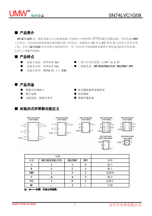
■产品简介74LVC1G08是一款的2输入与门集成电路,可实现和的数学逻辑运算。
采用先进CMOS 工艺设计,具有低功耗和高输出驱动能力的工作特点,电源电压VCC 在1.65V 和5.5V 之间芯片均可正常工作。
并且74LVC1G08具有多种小型封装外形,可广泛应用于高端精密仪器和小型化低功耗的手持设备,以及人工智能等领域。
■产品特点■产品用途■封装形式和管脚功能定义管脚名称DBV/DCK/DRL/YZPDRY/DSFDPW 说明A 112输入B 221输入GND 333电源地Y 445输出VCC 565电源正NC-5-空脚注:NC----空脚,内部无连接线,●便携式音频接口●蓝光播放器和家庭影院●数字电视●固态硬盘●无线耳机,智能手表等●智能穿戴设备●低输入电流:典型值0.1uA ●宽工作电压范围:1.65V to 5.5V●低静态功耗:典型值0.1uA ●封装形式:DBV/DCK/DRL/YZP/DRY/DSF/DPW●高输出驱动:VCC=4.5V,大于32MASN■极限参数参数符号极限值单位工作电压V CC 6.5V 输入V IN 、-0.5~6.5V 输出电压(1)V OUT -0.5~6.5V 单个管脚输出电流I OUT 25mA Vcc 或GND 电流I CC 50mA 存储温度T S -65-150℃引脚焊接温度T W260,10s℃注:1、在VCC=0V 断电状态下,输出所能承受的极限电压,2、极限参数是指无论在任何条件下都不能超过的极限值。
万一超过此极限值,将有可能造成产品劣化等物理性损伤;同时在接近极限参数下,不能保证芯片可以正常工作。
■原理逻辑图■真值表■工作条件项目符号测试条件最小值典型值最大值单位工作电压V CC - 1.65- 5.5V 输入高电平电压V IHV CC =1.65V~1.95V 0.65*V CC--VV CC =2.3V~2.7V 1.7V --V CC =3V~5.5V 0.7*V CC--输入高电平电压V IH V CC =1.65V~1.95V--0.35*V CCV V CC =2.3V~2.7V --0.7V CC =3V~5.5V--0.3*V CC输入电压V I -0- 5.5V 输出电压V O-0-V CC V高电平输出电流I OHV CC =1.65V---4mAV CC =2.3V ---8V CC =3V ---16V CC =4.5V ---32低电平输出电流I OLV CC =1.65V--4mAV CC =2.3V --8V CC =3V --16V CC =4.5V--32■电学特性直流电学特性:TA=25℃项目符号测试条件V CC典型值最大值单位高电平负载电压V OH I OH=-100uA 1.65V~5.5V 1.64-V I OH=-4mA 1.65V 1.47-I OH=-8mA 2.3V 2.15-I OH=-16mA3V 2.73-I OH=-32mA 4.5V 4.0低电平负载电压V OL I OH=100uA 1.65V~5.5V0.01-V I OH=4mA 1.65V0.11-I OH=8mA 2.3V0.11-I OH=16mA3V0.2-I OH=32mA 4.5V0.35-输入电流I I AV I=5.5V或GND0~5.5V0.01±5uA B0.01±5关断电流I OFF V I V I=5.5V00.01±10uA V O V O=5.5V00.01±10工作电流I CC V I=5.5V,I O=01.65V~5.5V0.0110uA V I=GND,I O=00.0110工作电流变化值 I CC A=V CC-0.6VB=V CC或GND3V~5.5V25-uA B=V CC-0.6VA=V CC或GND25-uA交流电学特性:Ta=25℃V CC=5.0V,t r=t f≤20ns见测试方法。
74LVC1G66GW-R资料

SOT886/SOT891 1 2 3 4 5 6
7. Functional description
Description
independent input or output independent output or input ground (0 V) enable input (active HIGH) not connected supply voltage
E Y
Fig 1. Logic symbol
Z 001aag487
1 1
4# X1
2 1
mna076
Fig 2. IEC logic symbol
Y E
Fig 3. Logic diagram
Z
VCC
mna658
74LVC1G66_6
Product data sheet
Rev. 06 — 27 August 2007
Symbol Parameter Conditions
−40 °C to +85 °C
−40 °C to +125 °C Unit
The 74LVC1G66 provides one single pole, single-throw analog switch function. It has two input/output terminals (Y and Z) and an active HIGH enable input pin (E). When E is LOW, the analog switch is turned off.
[2] Applies to control signal levels.
74LVC1G66_6
Product data sheet
- 1、下载文档前请自行甄别文档内容的完整性,平台不提供额外的编辑、内容补充、找答案等附加服务。
- 2、"仅部分预览"的文档,不可在线预览部分如存在完整性等问题,可反馈申请退款(可完整预览的文档不适用该条件!)。
- 3、如文档侵犯您的权益,请联系客服反馈,我们会尽快为您处理(人工客服工作时间:9:00-18:30)。
1/10April 2004s 5V TOLERANT INPUTSs HIGH SPEED:t PD =4.5ns (MAX.)at V CC =3V sLOW POWER DISSIPATION:I CC =1µA (MAX.)at T A =25°CsPOWER DOWN PROTECTION ON INPUTS AND OUTPUTSsSYMMETRICAL OUTPUT IMPEDANCE:|I OH |=I OL =24mA (MIN)at V CC =3V sBALANCED PROPAGATION DELAYS:t PLH ≅t PHLsOPERATING VOLTAGE RANGE:V CC (OPR)=1.65V to 5.5V (1.2V Data Retention)sIMPROVED LATCH-UP IMMUNITYDESCRIPTIONThe 74LX1G08is a low voltage CMOS SINGLE 2-INPUT AND GATE fabricated with sub-micron silicon gate and double-layer metal wiring C 2MOS technology.It is ideal for 1.65to 5.5V CC operations and low power and low noise applications.The internal circuit is composed of 3stages including bufferoutput,which provide high noise immunity and stable output.Power down protection is provided on input and output and 0to 7V can be accepted on inputs with no regard to the supply voltage.It can be interfaced to 5V signal environment for inputs in mixed 3.3/5V system.All inputs and outputs are equipped with protection circuits against static discharge.74LX1G08LOW VOLTAGE CMOS SINGLE 2-INPUT AND GATEWITH 5V TOLERANT INPUTPIN CONNECTION AND IEC LOGIC SYMBOLSORDER CODESPACKAGE T &R SOT23-5L 74LX1G08STR SOT323-5L74LX1G08CTR74LX1G082/10INPUT AND OUTPUT EQUIVALENT CIRCUITPIN DESCRIPTIONTRUTH TABLEABSOLUTE MAXIMUM RATINGSAbsolute Maximum Ratings are those values beyond which damage to the device may occur.Functional operation under these conditions isnot implied1)I O absolute maximum rating must be observed 2)V O <GND,V O >VCCPIN N°SYMBOL NAME AND FUNCTION 11A Data Input 21B Data Input 3GND Ground (0V)41Y Data Output5V CCPositive Supply VoltageA B Y L L L L H L H L L HHHSymbol ParameterValue Unit V CC Supply Voltage -0.5to +7.0V V I DC Input Voltage-0.5to +7.0V V O DC Output Voltage (V CC =0V)-0.5to +7.0V V O DC Output Voltage (High or Low State)(note 1)-0.5to V CC +0.5V I IK DC Input Diode Current-50mA I OK DC Output Diode Current (note 2)-50mA I ODC Output Current±50mA I CC or I GND DC V CC or Ground Current per Supply Pin±50mA T stgStorage Temperature -65to +150°C T LLead Temperature (10sec)300°C74LX1G083/10RECOMMENDED OPERATING CONDITIONS1)Truth Table guaranteed:1.2V to 3.6V 2)V IN from 0.8V to 2V at V CC =3.0VDC SPECIFICATIONSSymbol ParameterValue Unit V CC Supply Voltage (note 1) 1.65to 5.5V V I Input Voltage0to 5.5V V O Output Voltage (V CC =0V)0to 5.5V V O Output Voltage (High or Low State)0to V CC V I OH ,I OL High or Low Level Output Current (V CC =4.5to 5.5V)±32mA I OH ,I OL High or Low Level Output Current (V CC =3.0to 3.6V)±24mA I OH ,I OL High or Low Level Output Current (V CC =2.7to 3.0V)±12mA I OH ,I OL High or Low Level Output Current (V CC =2.3to 2.7V)±8mA I OH ,I OL High or Low Level Output Current (V CC =1.65to 2.3V)±4mA T op Operating Temperature-55to 125°C dt/dvInput Rise and Fall Time (note 2)0to 10ns/VSymbolParameterTest ConditionValueUnitV CC (V)-40to 85°C -55to 125°C Min.Max.Min.Max.V IHHigh Level Input Voltage1.65to 1.950.75V CC 0.75V CC V2.3to 2.70.7V CC 0.7V CC3.0to 5.50.7V CC0.7V CCV ILLow Level Input Voltage1.65to 1.950.25V CC 0.25V CC V2.3to 2.70.3V CC 0.3V CC3.0to 5.50.3V CC0.3V CCV OHHigh Level Output Voltage1.65to 4.5I O =-100µA V CC -0.1V CC -0.1V1.65I O =-4mA 1.2 1.22.3I O =-8mA 1.9 1.93.0I O =-16mA 2.4 2.4I O =-24mA 2.2 2.24.5I O =-32mA 3.83.8V OLLow Level Output Voltage1.65to 4.5I O =100µA 0.10.1V 1.65I O =4mA 0.450.452.3I O =8mA 0.30.33.0I O =16mA 0.40.4I O =24mA 0.550.554.5I O =32mA 0.550.55I I Input Leakage Current1.65to 5.5V I =0to 5.5V ±10±10µA I off Power Off Leakage Current0V I or V O =5.5V 1010µA I CCQuiescent Supply Current1.65to 5.5V I =V CC or GND1010µA74LX1G084/10AC ELECTRICAL CHARACTERISTICSCAPACITANCE CHARACTERISTICS1)C PD is defined as the value of the IC’s internal equivalent capacitance which is calculated from the operating current consumption without load.(Refer to Test Circuit).Average current can be obtained by the following equation.I CC(opr)=C PD x V CC x f IN +I CCSymbolParameterTest ConditionValueUnitV CC (V)C L (pF)R L (Ω)t s =t r (ns)-40to 85°C -55to 125°C Min.Max.Min.Max.t PLH t PHLPropagation Delay Time1.65to 1.95151M Ω 3.0212.0212.0ns2.3to 2.727.027.03.0to 3.614.71 4.74.5to5.51 4.11 4.11.65to 1.95301000 2.027.527.52.3to 2.730500 2.02 5.52 5.52.750500 2.51 5.21 5.23.0to 3.650500 2.51 4.21 4.24.5to 5.550500 2.513.713.7SymbolParameterTest ConditionValue UnitV CC (V)T A =25°C Min.Typ.Max.C IN Input Capacitance4pF C PDPower Dissipation Capacitance (note 1)1.8f IN =10MHz21pF 2.5243.32674LX1G085/10TEST CIRCUITT OUT TEST CIRCUIT AND WAVEFORM SYMBOL VALUEWAVEFORM:PROPAGATION DELAY (f=1MHz;50%duty cycle)SymbolV CC 1.65to 1.95V2.3to 2.7V 2.7to 5.5V C L 15pF/30pF 15pF/30pF 15pF/50pF R L 1M Ω/1000Ω1M Ω/500Ω1M Ω/500ΩV IH V CC V CC V CC V M V CC /2V CC /2V CC /2t r =t r<2.0ns<2.0ns<2.5ns74LX1G088/1074LX1G08Information furnished is believed to be accurate and reliable. However, STMicroelectronics assumes no responsibility for the consequences of use of such information nor for any infringement of patents or other rights of third parties which may result from its use. No license is granted by implication or otherwise under any patent or patent rights of STMicroelectronics. Specifications mentioned in this publication are subject to change without notice. This publication supersedes and replaces all information previously supplied. STMicroelectronics products are not authorized for use as critical components in life support devices or systems without express written approval of STMicroelectronics.The ST logo is a registered trademark of STMicroelectronicsAll other names are the property of their respective owners© 2004 STMicroelectronics - All Rights ReservedSTMicroelectronics GROUP OF COMPANIESAustralia - Belgium - Brazil - Canada - China - Czech Republic - Finland - France - Germany - Hong Kong - India - Israel - Italy - Japan - Malaysia - Malta - Morocco - Singapore - Spain - Sweden - Switzerland - United Kingdom - United States.10/10。