BHNW, 规格书,Datasheet 资料
启英泰伦 CI2311 数据手册说明书

CI2311数据手册高性能神经网络智能语音芯片TSSOP24长7.8mm 宽6.4mm 高1.2mm•脑神经网络处理器(BNPU)–BNPU V3,支持DNN\TDNN\RNN\CNN 等神经网络及并行矢量运算,可实现语音识别、声纹识别、命令词自学习、语音检测及深度学习降噪等功能•CPU 和存储器–CPU 主频可达240MHz –内置1MBytes Flash 存储器–内置640KBytes SRAM–内置512bit eFuse,可用于应用加密•Audio Codec–高性能低功耗audio ADC,SNR ≥95dB –低功耗audio DAC,SNR ≥95dB •音频接口–1路双通道PDM 接口•ADC 和PWM–内置2通道12bit SAR ADC –支持3路PWM 接口•GPIO–7个高速GPIO,响应速率可达20MHz –其中5个GPIO 支持5V 输入•复位和电源管理–内置电源管理单元PMU–PMU 输入电压范围:3.6V 到5.5V –内置上电复位(POR)–内置电压检测(PVD)•时钟–16MHz 外接晶体振荡器•通讯接口–1路IIC 接口–2路UART 接口,支持5V 通讯,支持最高3Mbps 速率•定时器和看门狗–内置4组32位定时器和2组看门狗•无线–GFSK 调制方式,1Mbps 模式的接收灵敏度可达-90dBm–最大发射输出功率达+8dBm –支持BLE 广播–频道切换快,可以实现多频道调频算法目录1概述 (3)1.1功能描述 (3)1.2芯片规格 (4)2引脚图和功能描述 (7)2.1引脚图 (7)2.2管脚描述 (8)2.3复用功能 (10)3电气特性 (11)4无线特性 (12)5封装信息 (13)6订购信息 (14)7应用方案 (15)7.1应用参考电路图 (15)7.2应用其它注意事项 (16)1概述1.1功能描述CI2311是启英泰伦研发的新一代高性能神经网络智能语音芯片,集成了启英泰伦自研的脑神经网络处理器BNPU V3和CPU内核,系统主频可达240MHz,内置高达640KByte的SRAM,集成PMU电源管理单元,集成双通道高性能低功耗Audio Codec和多路UART、IIC、PWM、GPIO、PDM等外围控制接口,集成2.400~2.483GHz世界通用ISM频段无线收发芯片,嵌入了基带通讯协议。
华宏光电子(深圳)有限公司 3528单晶蓝光贴片产品说明书

产品规格书Specification3528单晶蓝光贴片3528 Single Chip Blue Color Top LED产品型号/ Part No : WW-BNA30TS-Q1批准审核制定牛焕东陶源杨成琼华宏光电子(深圳)有限公司WAH WANG OPTOELECTRONIC (SHENZHEN)COMPANY LIMITED地址:深圳市宝安区大浪街道华荣路联建科技工业园第五栋Address:Floor Block 5, Lianjian Science &Technology lndustrial Park,Crossing of HuaRong Road,Dalang Sub-District, Bao`an, ShenZhen电话:*************Tel**************传真:*************Fax**************S.D.N. / D.N. No. 送货单编号Customer Name客户名称Sample Approval Signature戶客确认签署Date日期■ 产品特性■ Features:PLCC LED dimensions: 3.5(L) x 2.8(W) x 1.9(H) mm 发散视角120°Wide view angle 120 环保防静电胶带包装Available on tape and reel with Anti-electrostatic bag 产品性能稳定可靠Compatible for all SMT Assembly and Lead-Free SolderingRoHS Compliant■ 应用■ Applications: 背光液晶开关和显示Backlight for LCD Switch and Display 装饰照明Decorative Lighting 一般照明General Lighting 汽车内部照明Automotive Interior Lighting 常规使用General Use■ 产品尺寸图■ Package Dimensions:2建议焊盘尺寸■ 注释■ Notes :1、上图所有尺寸的单位为毫米All dimension units are in millimeters.2、所有外形尺寸公差为 ± 0.25毫米,除非另有说明All dimension tolerances are ± 0.25mm unless otherwise noted.■ 最大绝对额定值■ Absolute Maximum Ratings :参数Parameter 符号 Symbol 数值 Value单位 Unit 功耗Power dissipation P d 60 mW 连续正向电流I F 20 mA 峰值正向电流 Peak Forward CurrentI FP 50 mA 反向电压 Reverse Voltage V R5V静电放电(HBM)ESD 1000 V 工作温度范围T opr -25 to +85 ℃ 存储温度范围T stg -40 to +100 ℃ 无铅焊接温度T sol260( for 5 sec)℃Recommended Soldering Pads Dimensions Recommended Soldering Pads Dimensions光电参数规格:Electrical Optical Characteristics:WW-BNA30TS-Q1注释Notes:1、发光强度、功耗和光通量的误差为 ± 10%WW maintains a tolerance of ±10% on flux and power measurements.2、波长的误差为 ±1nm;d ±1nm.3、电压的误差为 ± 0.1VA tolerance of ±0.1V on forward voltage measurements参数 Parameter 符号 Symbol最小值 Min.平均值Typ.最大值 Max.单位 Unit测试条件 Test Conditions发光强度I v 400 --- 600 mcd波长 Spectral λd465 --- 475 nm参考光通量 Φv ------- --- lm 正向电压 V F 2.7 --- 3.3 V 视角Viewing Angle 2θ1/2 ---120 --- Deg I F =20mA反向电流 I R --- --- 5 µA V R = 5V■光电特性Typical Optical Characteristics CurvesAmbient Temperature TA(°C)环境温度(℃)R e l a t i v e L u m i n o u s I n t e n s i t y (%)发光强度(%)Forward Current Derating Curve 环境温度与电流的关系曲线图Radiation Diagram发光角度图Spectral Distribution波长曲线图Luminous Intensity vs AmbientTemperature发光强度与温度的关系曲线图F o r w a r d C u r r e n t (m A )电流(m A )Ambient Temperature TA(°C)R e l a t i v e L u m i n o u s I n t e n s i t y (%)光通量(%)Forward Current (mA)电流(mA)Forward Voltage (V)电压(V)F o r w a r d C u r r e n t (m A ) 电流(m A )Forward Current vs Forward Voltage伏安特性曲线Forward Current vs Relative Luminous Intensity电流和光通量的关系■ 产品可靠性检测项目:序號No.实验项目Test Item标准测试方法Standard TestMethod测试条件Test Conditions检测时间和周期Duration不良数/测试数Failure RateIf=20mA1正常工作寿命Steady StateOperating LifeJEITA ED-4701100 103 Ta=25℃1000hrs 0/22 JEITA ED-47012低温贮藏Low TemperatureStorage 200 202Ta=-40℃ 1000hrs 0/22JEITA ED-47013高温贮存High TemperatureStorage 200 201Ta=100℃ 1000hrs 0/22JEITA ED-4701 Ta=60℃4高温高湿贮藏TemperatureHumidity Storage 100 103 RH=90%1000hrs 0/22JEITA ED-4701 0℃ ~ +100℃5 冷热冲击Thermal Shock 300 307 5min~ 15sec ~5min10 cycles 0/22H:+100℃ 30min.高低温循环Temperature Cycle ∫ : +25℃ 5min.6 JEITA ED-4701100 105L:-40℃ 30min100cycles0/22 JEITA ED-47017 烫锡Solder Heat 300 301 Tsld=260℃, 10sec(Max.)2 times 0/22■ 失效产品判定标准:项目Item符号Symbol测试条件Test Condition最小值Min.最大值Max.正向电压Forward VoltageV F I F = 20mA -- *U.S.L×1.1 反向电流Reverse CurrentI R V R = 5V -- *U.S.L×2.0发光强度Luminous IntensityI V I F = 20mA **L.S.L×0.7 --*U.S.L.:超出标准最大值*U.S.L.: Upper Standard Level** L.S.L.:低于标准最低值** L.S.L.: Lower Standard Level■ .■■■ Dimensions of the reel:■ .包装■ Packing:防潮、防静电真空密封包装■ Moisture, anti-static vacuum sealed packages■ 注释■ Note:上图所有尺寸的单位为毫米,公差为 ± 2.0毫米,除非另有说明All dimensions are in mm, tolerance is ± 2.0mm unless otherwise noted.■注意事项:PRECAUTION IN USE1.存储要求:1.1推荐储存环境温度:5℃30℃的(41oF86oF)湿度:相对湿度60%以下1.2防潮袋密封包装储存时间3个月,起始时间以包装标签日期为准,需在包装袋封口良好并无漏气现象,且湿度卡未变为粉红色前提下使用,如超过3个月的LED需按2. 2要求除潮烘烤后才能正常使用。
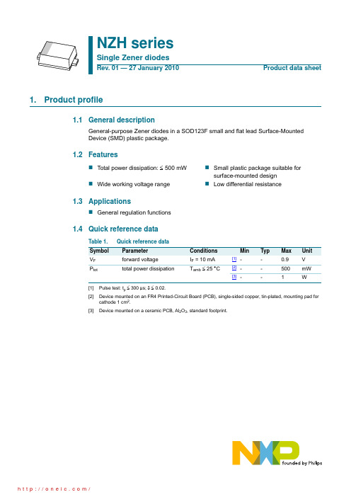
NZH3V0B,115;NZH10C,115;NZH8V2B,115;NZH7V5C,115;NZH6V2B,115;中文规格书,Datasheet资料
thermal resistance from junction to solder point
Min Typ Max Unit
[1] -
-
250 K/W
[2] -
-
125 K/W
[3] -
-
70 K/W
[1] Device mounted on an FR4 PCB, single-sided copper, tin-plated, mounting pad for cathode 1 cm2. [2] Device mounted on a ceramic PCB, Al2O3, standard footprint. [3] Soldering point of cathode tab.
Version SOD123F
Table 4. Marking codes
Type number
Marking code
NZH3V0B
CH
NZH3V3A
CJ
NZH3V6B
CK
NZH3V9B
CL
NZH4V3B
CM
NZH4V7B
CN
NZH5V1B
CP
NZH5V6B
CQ
NZH6V2B
CR
NZH6V8B
CS
5. Limiting values
Table 5. Limiting values In accordance with the Absolute Maximum Rating System (IEC 60134).
Symbol Parameter
Conditions
Min
Max Unit
IF Ptot
NZHxxx
FSBH0270NY;FSBH0170NY;FSBH0170WNY;FSBH0270WNY;FSBH0370NY;中文规格书,Datasheet资料
Green Mode Fairchild Power Switch (FPS™)FeaturesBrownout Protection with HysteresisBuilt-In 5ms Soft-Start FunctionInternal Avalanche-Rugged 700V SenseFETNo Acoustic Noise During Light-Load Operation High-Voltage StartupLinearly Decreasing PWM Frequency to 18KHz Peak-Current-Mode ControlCycle-by-Cycle Current LimitingLeading-Edge Blanking (LEB)Synchronized Slope CompensationInternal Open-Loop ProtectionV DD Under-Voltage Lockout (UVLO)V DD Over-Voltage Protection (OVP)Internal Auto-Restart Circuit (OVP, OTP)Constant Power Limit (Full AC Input Range)Internal OTP Sensor with HysteresisVIN Pin for Pull-HIGH Latch Function and Pull-LOW Auto-Recovery Protection ApplicationsGeneral-purpose switch-mode power supplies and flyback power converters, including:Auxiliary Power Supply for PC and ServerSMPS for VCR, SVR, STB, DVD & DVCD Player, Printer, Facsimile, and ScannerAdapter for Camcorder DescriptionThe highly integrated FSBH-series consists of an integrated current-mode Pulse Width Modulator (PWM) and an avalanche-rugged 700V SenseFET. It is specifically designed for high-performance offline Switch Mode Power Supplies (SMPS) with minimal external components.The integrated PWM controller features include a proprietary green-mode function that provides off-time modulation to linearly decrease the switching frequency at light-load conditions to minimize standby power consumption. To avoid acoustic-noise problems, the minimum PWM frequency is set above 18kHz. This green-mode function enables the power supply to meet international power conservation requirements.The PWM controller is manufactured using the BiCMOS process to further reduce power consumption. The FSBH-series turns off some internal circuits to improve power saving when V FB is lower than 1.6V, which allows an operating current of only 2.5mA.The FSBH-series has built-in synchronized slope compensation to achieve stable peak-current-mode control. The proprietary external line compensation ensures constant output power limit over a wide AC input voltage range, from 90V AC to 264V AC.The FSBH-series provides many protection functions. In addition to cycle-by-cycle current limiting, the internal open-loop protection circuit ensures safety when an open-loop or output short occurs. PWM output is disabled until V DD drops below the V TH-OLP, then the controller starts up again. As long as V DD exceeds 28V, the internal OVP circuit is triggered.Compared with a discrete MOSFET and controller or RCC switching converter solution, the FSBH-series reduces total component count, design size, and weight; while increasing efficiency, productivity, andFSBH0F70A, FSBH0170/A, FSBH0270/A, FSBH0370 — Green Mode Fairchild Power Switch (FPS™) 8-Pin Dual In-Line Package (DIP) Tube FSBH0270ANY 2.0A 700V -40°C to +105°C FSBH0170NY 1.0A 700V -40°C to +105°C Enabled FSBH0270NY 2.0A 700V -40°C to +105°C FSBH0370NY 3.0A 700V -40°C to +105°C Application Diagram HV Drain GND VDD FB VIN Figure 1. Typical Flyback Application Output Power Table (1)Product 230V AC ± 15%(2) 85-265V AC Adapter(3) Open Frame(4) Adapter(3) Open Frame(4)FSBH0F70A 7W 10W 6W 8W FSBH0170/A 10W 15W 9W 13W FSBH0270/A 14W 20W 11W 16W FSBH0370 17.5W 25W 13W 19W Notes: 1. The maximum output power can be limited by junction temperature. 2. 230 V AC or 100/115 V AC with doublers.FSBH0F70A, FSBH0170/A, FSBH0270/A, FSBH0370 Green — Mode Fairchild Power Switch (FPS™) Internal Block DiagramsFigure 2. FSBH0170, FSBH0270, FSBH0370 Internal Block DiagramFigure 3. FSBH0F70A, FSBH0170A, FSBH0270A Internal Block DiagramFSBH0F70A, FSBH0170/A, FSBH0270/A, FSBH0370 Green — Mode Fairchild Power Switch (FPS™) 0246-40-25-105203550658095110125Temperature(°C)I D D- 2.862.882.902.92-40-25-105203550658095110125Temperature(°C)I D D-Figure 6. I DD-ST vs. Temperature Figure 7. I DD-OP vs. Temperature 11.211.411.611.812.012.212.4-40-25-105203550658095110125Temperature(°C)V D D-O N(V)7.77.87.98.08.18.28.3-40-25-105203550658095110125Temperature(°C)V D D-O F F(V)Figure 8. V DD-ON vs. Temperature Figure 9. V DD-OFF vs. Temperature 5.05.25.45.65.86.06.26.46.6-40-25-105203550658095110125Temperature(°C)V T H-O L P(V)28.3528.3628.3728.3828.3928.4028.4128.42-40-25-105203550658095110125Temperature(°C)V D D-O V P(V)Figure 10. V TH-OLP vs. Temperature Figure 11. V DD-OVP vs. Temperature 2.53.03.54.0H V(m A)34567V-L C(µA)FSBH0F70A, FSBH0170/A, FSBH0270/A, FSBH0370 — Green Mode Fairchild Power Switch (FPS™) 97.598.098.599.0-40-25-105203550658095110125Temperature(°C)F O S18.618.718.8-40-25-105203550658095110125Temperature(°C)F O S C Figure 14. f OSC vs. Temperature Figure 15. f OSC-G vs. Temperature 0.580.590.600.610.620.630.64-40-25-105203550658095110125Temperature(°C)V I N-O F F(V) 1.111.121.131.141.151.161.17-40-25-105203550658095110125Temperature(°C)V I N-O N(V)Figure 16. V IN-OFF vs. Temperature Figure 17. V IN-ON vs. Temperature 4.574.584.594.604.614.624.63-40-25-105203550658095110125Temperature(°C)V I N-H(V)0.280.290.300.310.320.330.34-40-25-105203550658095110125Temperature(°C)V I N-L(V)Figure 18. V IN-H vs. Temperature Figure 19. V IN-L vs. Temperature 4.504.554.604.654.704.75V F B-O L P(V) 2.402.452.502.552.60V F B-N(V)分销商库存信息:FAIRCHILDFSBH0270NY FSBH0170NY FSBH0170WNY FSBH0270WNY FSBH0370NY FSBH0F70ANY FSBH0170ANY FSBH0270ANY。
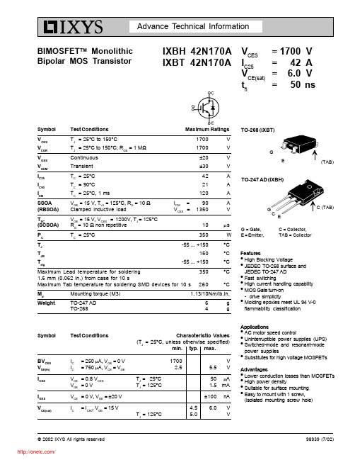
IXBH42N170A;IXBT42N170A;中文规格书,Datasheet资料
5,049,961 5,063,307
5,187,117 5,237,481
5,486,715 6,306,728B1 5,381,025
分销商库存信息:
IXYS IXBH42N170A
IXBT42N170A
Characteristic Values (TJ = 25°C, unless otherwise specified)
min. typ. max.
TJ = 25°C TJ = 125°C TJ = 125°C
1700 2.5
V 5.5 V
50 µA 1.5 mA
±100 nA
4.5 6.0 V
5.0
Advantages z Lower conduction losses than MOSFETs z High power density z Suitable for surface mounting z Easy to mount with 1 screw,
(isolated mounting screw hole)
IXYS MOSFETs and IGBTs are covered by one or more of the following U.S. patents:
4,835,592 4,850,072
4,881,106 4,931,844
5,017,508 5,034,796
/
TC = 90°C
ICM
TC = 25°C, 1 ms
42
A
21
A
120
A
SSOA (RBSOA)
VGE = 15 V, TVJ = 125°C, RG = 10 Ω Clamped inductive load
霍尼韦尔氢气纯度仪说明书模板
目录1.前言………………………………………………………………………………2 1.1概述……………………………………………………………….........2 1.2传感单元 (2)1.37866数字控制器 (3)1.4操作原理 (4)2.技术参数和选型 (6)2.1技术参数……………………………………………………………………62.2选型 (8)3.安装……………………………………………………………………….........9 3.1传感单元要求条件和定位 (9)3.2安装传感单元 (9)3.3管路连接 (9)3.4传感单元与数字控制器接线 (10)4.设置模式………………………………………………………………………11 4.1概述………………………………………………………………………11 4.2结构概述……………………………………………………………………...11 4.3单元设置组群 (11)4.4报警设置组群 (12)4.5M o d B U S通讯设置组群 (12)4.6校准组群………………………………………………………………………13 4.7状态组群………………………………………………………………………13 5.校准……………………………………………………………………………14 5.1概述……………………………………………………………………...14 5.2传感单元校准 (14)5.37866分析仪输入校准 (14)5.4模拟输出校准 (15)5.7安全锁定……………………………………………………………………...16 5.8设置报警极限 (17)6.操作………………………………………………………………………………18 6.1启动………………………………………………………………………18 7.排除故障…………………………………………………………………………19 7.1概述……………………………………………………………………...19 7.27866数字控制器检测 (20)附录 (21)1.前言1.1 概述美国HONEYWELL公司7866氢气纯度分析仪由三个基本部件组成: 传感单元( 变送器) , 控制单元( 接收器) ( 图1-1) 和电源。
FDMF6820A;中文规格书,Datasheet资料
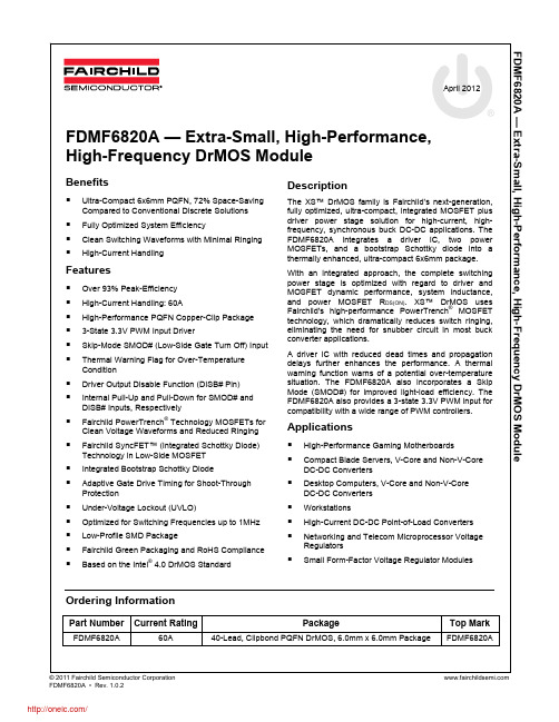
PHASE Switch node pin for bootstrap capacitor routing. Electrically shorted to VSWH pin. NC VIN
Switch node input. Provides return for high-side bootstrapped driver and acts as a sense point VSWH for the adaptive shoot-through protection. PGND GL THWN# DISB# PWM Power ground. Output stage ground. Source pin of the low-side MOSFET. For manufacturing test only. This pin must float; it must not be connected to any pin. Thermal warning flag, open collector output. When temperature exceeds the trip limit, the output is pulled LOW. THWN# does not disable the module. Output disable. When LOW, this pin disables the power MOSFET switching (GH and GL are held LOW). This pin has a 10µA internal pull-down current source. Do not add a noise filter capacitor. PWM signal input. This pin accepts a three-state 3.3V PWM signal from the controller.
SS12SDP2;SS22SDP2;SS14MDP2;SS12SDH2;SS12SBP2;中文规格书,Datasheet资料
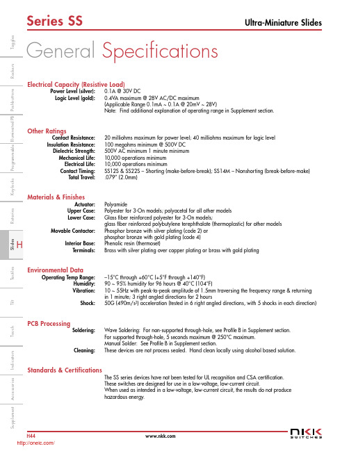
Series SSUltra-Miniature SlidesH44I n d i c a t o r sA c c e s s o r i e sS u p p l e m e n t T a c t i l e sK e y l o c k sR o t a r i e s P u s h b u t t o n sI l l u m i n a t e d P B P r o g r a m m a b l e R o c k e r sT o u c hT i l t T o g g l e sElectrical Capacity (Resistive Load)Power Level (silver): 0.1A @ 30V DCLogic Level (gold):0.4VA maximum @ 28V AC/DC maximum(Applicable Range 0.1mA ~ 0.1A @ 20mV ~ 28V)Note: Find additional explanation of operating range in Supplement section.Other RatingsContact Resistance: 20 milliohms maximum for power level; 40 milliohms maximum for logic level Insulation Resistance: 100 megohms minimum @ 500V DC Dielectric Strength: 500V AC minimum 1 minute minimum Mechanical Life: 10,000 operations minimum Electrical Life: 10,000 operations minimumContact Timing:SS12S & SS22S – Shorting (make-before-break); SS14M – Nonshorting (break-before-make)Total Travel: .079” (2.0mm)Materials & FinishesActuator: PolyamideUpper Case: Polyester for 3-On models; polyacetal for all other models Lower Case:Glass fiber reinforced polyester for 3-On models;glass fiber reinforced polybutylene terephthalate (thermoplastic) for other models Movable Contactor:Phosphor bronze with silver plating (code 2) orphosphor bronze with gold plating (code 4) Interior Base: Phenolic resin (thermoset)Terminals: Brass with silver plating over copper plating or brass with gold platingEnvironmental DataOperating Temp Range:–15°C through +60°C (+5°F through +140°F) Humidity: 90 ~ 95% humidity for 96 hours @ 40°C (104°F)Vibration:10 ~ 55Hz with peak-to-peak amplitude of 1.5mm traversing the frequency range & returning in 1 minute; 3 right angled directions for 2 hoursShock: 50G (490m/s 2) acceleration (tested in 6 right angled directions, with 5 shocks in each direction)PCB ProcessingSoldering:Wave Soldering: For non-supported through-hole, see Profile B in Supplement section. For supported through-hole, 5 seconds maximum @ 250°C maximum.Manual Solder: See Profile B in Supplement section.Cleaning: These devices are not process sealed. Hand clean locally using alcohol based solution.Standards & CertificationsThe SS series devices have not been tested for UL recognition and CSA certification. These switches are designed for use in a low-voltage, low-current circuit.When used as intended in a low-voltage, low-current circuit, the results do not producehazardous energy.General Specifications/Series SSUltra-Miniature Slides H45I n d i c a t o r sA c c e s s o r i e s S u p p l e m e n t T a c t i l e s Ke y l o c k s R o t a r i e s P u s h b u t t o n sI l l u m i n a t e d P B P r o g r a m m a b l e R o c k e r sT o u c h T i l t T o g g l e sTop or side actuation permits flexible board pact dimensions and low profile allow high density mounting and close stacking of PC boards.Crisp actuation positively indicates circuit status.Double molded thermoset base and thermo- plastic housing prevent loosening of terminals due to high soldering temperatures.Award-winning STC mechanism with benefitsunavailable in conventional mechanisms: smoother, positive detend actuation, increased contact stability, and unparalleled logic-level reliability. (Additional STC details in Terms and Acronyms in the Supplement section.)Insert molded terminals lock out flux, solvents, and other contaminants.Inch or metric terminal spacing for standard PC board grid (.100” x .100” or 2.0mm x 2.0mm).Actual SizeDistinctive Characteristics/Series SSUltra-Miniature SlidesH46I n d i c a t o r sA c c e s s o r i e sS u p p l e m e ntT a c t i l e sK e y l o c k sR o t a r i e s P u s h b u t t o n s I l l u m i n a t e d P BP r o g r a m m a b l e R o c k e r sT o u c hT i l t T o g g l e sTYPICAL SWITCH ORDERING EXAMPLESPDT ON-NONE-ON Circuit Terminals with .100” SpacingTop ActuatedSilver Contacts Rated 0.1A @ 30V DCDESCRIPTION FOR TYPICAL ORDERING EXAMPLESS12SDP2* 14M SP3T ON ON ON SS14M model has nonshorting contacts.22SDPDTONNONEONSS22S model has shorting contacts.See Poles & Circuits chart below.* 14M Circuit with silver contacts only./Series SSUltra-Miniature Slides H47I n d i c a t o r sA c c e s s o r i e sS u p p l e m e n t T a c t i l e s K e y l o c k sR o t a r i e sP u s h b u t t o nsI l l u m i n a t e d P BP r o g r a m m a b l e R o c k e rsT o u c h T il tT o g g l e sTERMINAL SPACINGCONTACT MATERIALS & RATINGSComplete explanation of operating range in Supplement section.2Gold over Silver/Phosphor Bronze Logic Level0.4VA max @ 28V AC/DC maxSilver over Phosphor Bronze Power Level 0.1A @ 30V DC4PSide ActuatedTop ActuatedHACTUATIONBInch .100” x .100” with Gray BaseMetric 2.0mm x 2.0mm with Black BaseDOn-None-On Single Pole Models On-None-On Double Pole Models 3-On ModelsOn-None-On Single Pole Models On-None-On Double Pole Models3-On Models.079.100.157/Series SSUltra-Miniature SlidesH48I n d i c a t o r sA c c e s s o r i e sS u p p l e m e n tT a c t i l e sK e y l o cksR o t a r i esP u s h b u t t o nsI l l u m i n a t e d P BP r o g ra m m ab l e R oc k e r sT o u c hT i l tT o g g le sTYPICAL SWITCH DIMENSIONSTop ActuatedSingle & Double PoleSide Actuated Single & Double PoleSS12SDP2SS12SDH23-On Circuit • Top Actuated Single PoleSS14MDP2SS14MDH2.079.0793-On Circuit • Side Actuated Single Pole/分销商库存信息:NKK-SWITCHSS12SDP2SS22SDP2SS14MDP2 SS12SDH2SS12SBP2SS22SDH2 SS22SBP2SS22SBH2SS14MDH2 SS14MBP2SS12SBH4SS22SDH4 SS12SBH2SS12SBP4SS12SDH4 SS12SDP4SS22SBP4。
DK-PS21767;DK-PS21765;中文规格书,Datasheet资料
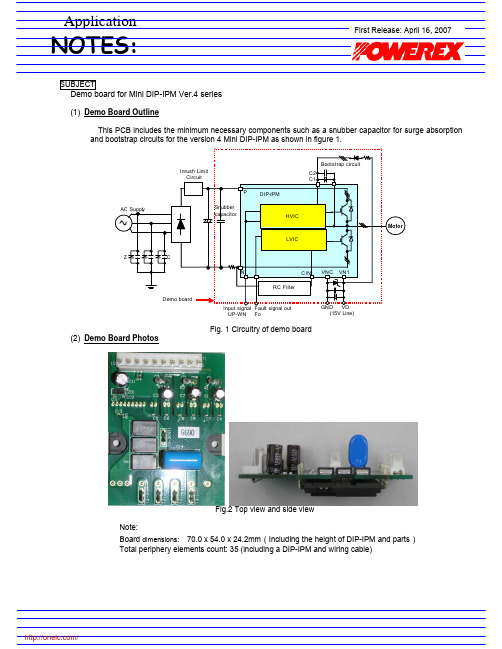
SUBJECTDemo board for Mini DIP-IPM Ver.4 series(1) Demo Board OutlineThis PCB includes the minimum necessary components such as a snubber capacitor for surge absorption and bootstrap circuits for the version 4 Mini DIP-IPM as shown in figure 1.(15V Line)FoUP-WNFig. 1 Circuitry of demo board(2) Demo Board PhotosFig.2 Top view and side viewNote:Board dimensions: 70.0 x 54.0 x 24.2mm (Including the height of DIP-IPM and parts ) Total periphery elements count: 35 (including a DIP-IPM and wiring cable)(3) Demo Board OutlinesFig.3 Patterns of front face and back face(4) Circuit schematicUVWPN1VP UN FO Fig.4 Circuit schematicNote: Although there is no zener diode mounted to P-side three floating drive supplies (between V UFB -V UFS ,V VFB -V VFS , V WFB -V WFS ) on this demo board, it is highly recommend to add these zener diodes in actual system board.(5) Parts listTable 1 Parts listThe demo board kit includes an input signal connection cable and a power supply cable with a connector. The input signal cable should be cut to make the connection between MCU/DSP and the demo board as short as possible.Symbol Type Name DescriptionNoteD1 10DRA60 1A 600V Diode Japan International D2 10DRA60 1A 600V Diode Japan International D3 10DRA60 1A 600V Diode Japan International ZD1 U1ZB24 24V 1W Zener DiodeToshiba C1 UPW1H220MDD 22µF50V Al electrolytic capacitor Nichicon C2 UPW1H220MDD 22µF50V Al electrolytic capacitor Nichicon C3 UPW1H220MDD 22µF50V Al electrolytic capacitor Nichicon C4 C1608X7R1H102K 1000pF50V ceramic capacitor TDK C5 C1608X7R1H102K 1000pF50V ceramic capacitor TDK C6 C1608X7R1H102K 1000pF50V ceramic capacitor TDK C7 C1608X7R1H102K 1000pF50V ceramic capacitor TDK C8 C1608X7R1H102K 1000pF50V ceramic capacitor TDK C9 C1608X7R1H102K 1000pF50V ceramic capacitor TDK C10 C1608X7R1H102K 1000pF50V ceramic capacitor TDK C11 UPW1H470MED 47µF50V Al electrolytic capacitor Nichicon C12 GRM39R223K50 0.022µF50V ceramic capacitorMurata C13 C1608X7R1H102K 1000pF50V ceramic capacitor TDK C14MDDSA0.22µF630V0.22µF630V snubber capacitorHitachi AIC R1 RK73H1JTD10F 1/16W 10ΩF Hokuriku Denko R2 RK73H1JTD10F 1/16W 10Ω F Hokuriku Denko R3 RK73H1JTD10F 1/16W 10Ω F Hokuriku Denko R4 RK73H1JTD10kF 1/16W 10K Ω F Hokuriku Denko R5 RK73H1JTD2kF 1/16W 2K Ω F Hokuriku DenkoR6-1 SL2TBK33/47LOF PS21765: 47m Ω, ±1%, 2WX3PS21767: 33m Ω, ±1%, 2WX3 KOA, Current detecting resistor R6-2 SL2TBK33/47LOF R6-3 SL2TBK33/47LOF T1 B10P-VH 10pin Socket JST T2-1 TP42097-21 Fasten tab Kyoushin T2-2 TP42097-21 Fasten tab Kyoushin T2-3 TP42097-21 Fasten tab Kyoushin T3-1 TP42097-21 Fasten tab Kyoushin T3-2 TP42097-21Fasten tabKyoushin IPM PS21765/PS21767 20A/30A mini DIP-IPMMitsubishiWiring cable JST分销商库存信息:POWEREXDK-PS21767DK-PS21765。
744710215;中文规格书,Datasheet资料

5.1 5.0 4.02012-06-272012-05-022009-06-30SStSStRStSStCZWürth Elektronik eiSos GmbH & Co. KGEMC & Inductive SolutionsMax-Eyth-Str. 174638 WaldenburgGermanyTel. +49 (0) 79 42 945 - 0A Dimensions: [mm]F Typical Impedance Characteristics:H4: Classification Wave Soldering Profile:H5: Classification Wave ProfileProfile FeaturePreheat- Temperature Min (T smin )- Temperature Typical (T stypical ) - Temperature Max (T smax ) - Time (t s ) from (T smin to T smax )Δ preheat to max Temperature Peak temperature (T p )Time of actual peak temperature (t p )Ramp-down rate - Min - Typical - MaxTime 25°C to 25°C Pb-Free Assembly 100°C 120°C 130°C 70 seconds 150°C max.250°C - 260°C max. 10 secondsmax. 5 second each wave ~ 2 K/s ~ 3.5 K/s ~ 5 K/s 4 minutesSn-Pb Assembly 100°C 120°C 130°C 70 seconds 150°C max.235°C - 260°C max. 10 secondsmax. 5 second each wave ~ 2 K/s ~ 3.5 K/s ~ 5 K/s 4 minutesrefer to EN 61760-1:2006H Soldering Specifications:I Cautions and Warnings:The following conditions apply to all goods within the product series of WE-SDof Würth Elektronik eiSos GmbH & Co. KG:General:All recommendations according to the general technical specifications of the data-sheet have to be complied with.The disposal and operation of the product within ambient conditions which probably alloy or harm the wire isolation has to be avoided.If the product is potted in customer applications, the potting material might shrink during and after hardening. Accordingly to this the product is exposed to the pressure of the potting material with the effect that the core, wire and termination is possibly damaged by this pressure and so the electrical as well as the mechanical characteristics are endanger to be affected. After the potting material is cured, the core, wire and termination of the product have to be checked if any reduced electrical or mechanical functions or destructions have occurred.The responsibility for the applicability of customer specific products and use in a particular customer design is always within the authority of the customer. All technical specifications for standard products do also apply for customer specific products.Washing varnish agent that is used during the production to clean the application might damage or change the characteristics of the wire in-sulation, the marking or the plating. The washing varnish agent could have a negative effect on the long turn function of the product.Direct mechanical impact to the product shall be prevented as the ferrite material of the core could flake or in the worst case it could break. Product specific:Follow all instructions mentioned in the datasheet, especially:•The solder profile has to be complied with according to the technical wave soldering specification, otherwise no warranty will be sustai-ned.•All products are supposed to be used before the end of the period of 12 months based on the product date-code, if not a 100% solderabi-lity can´t be warranted.•Violation of the technical product specifications such as exceeding the nominal rated current will result in the loss of warranty.1. General Customer ResponsibilitySome goods within the product range of Würth Elektronik eiSos GmbH & Co. KG contain statements regarding general suitability for certain application areas. These statements about suitability are based on our knowledge and experience of typical requirements concerning the are-as, serve as general guidance and cannot be estimated as binding statements about the suitability for a customer application. The responsibi-lity for the applicability and use in a particular customer design is always solely within the authority of the customer. Due to this fact it is up to the customer to evaluate, where appropriate to investigate and decide whether the device with the specific product characteristics described in the product specification is valid and suitable for the respective customer application or not.2. Customer Responsibility related to Specific, in particular Safety-Relevant ApplicationsIt has to be clearly pointed out that the possibility of a malfunction of electronic components or failure before the end of the usual lifetime can-not be completely eliminated in the current state of the art, even if the products are operated within the range of the specifications.In certain customer applications requiring a very high level of safety and especially in customer applications in which the malfunction or failure of an electronic component could endanger human life or health it must be ensured by most advanced technological aid of suitable design of the customer application that no injury or damage is caused to third parties in the event of malfunction or failure of an electronic component.3. Best Care and AttentionAny product-specific notes, warnings and cautions must be strictly observed.4. Customer Support for Product SpecificationsSome products within the product range may contain substances which are subject to restrictions in certain jurisdictions in order to serve spe-cific technical requirements. Necessary information is available on request. In this case the field sales engineer or the internal sales person in charge should be contacted who will be happy to support in this matter.5. Product R&DDue to constant product improvement product specifications may change from time to time. As a standard reporting procedure of the Product Change Notification (PCN) according to the JEDEC-Standard inform about minor and major changes. In case of further queries regarding the PCN, the field sales engineer or the internal sales person in charge should be contacted. The basic responsibility of the customer as per Secti-on 1 and 2 remains unaffected.6. Product Life CycleDue to technical progress and economical evaluation we also reserve the right to discontinue production and delivery of products. As a stan-dard reporting procedure of the Product Termination Notification (PTN) according to the JEDEC-Standard we will inform at an early stage about inevitable product discontinuance. According to this we cannot guarantee that all products within our product range will always be available. Therefore it needs to be verified with the field sales engineer or the internal sales person in charge about the current product availability ex-pectancy before or when the product for application design-in disposal is considered.The approach named above does not apply in the case of individual agreements deviating from the foregoing for customer-specific products.7. Property RightsAll the rights for contractual products produced by Würth Elektronik eiSos GmbH & Co. KG on the basis of ideas, development contracts as well as models or templates that are subject to copyright, patent or commercial protection supplied to the customer will remain with Würth Elektronik eiSos GmbH & Co. KG.8. General Terms and ConditionsUnless otherwise agreed in individual contracts, all orders are subject to the current version of the “General Terms and Conditions of Würth Elektronik eiSos Group”, last version available at .J Important Notes:The following conditions apply to all goods within the product range of Würth Elektronik eiSos GmbH & Co. KG:分销商库存信息: WURTH-ELECTRONICS 744710215。
ADL024-14E;中文规格书,Datasheet资料

Data SheetADL-SeriesNanopower Digital SwitchesKey Features• Ultraminiature 1.1 mm x 1.1 mm x 0.45 mm ULLGA package• Precise Detection of Low Magnetic Fields• Low Voltage Operation to 2.4 V• Typical Power Consumption As Low As 72 nW at 2.4 V• Digital Switch Output• Continuously Operating or Duty-Cycled VersionsDescriptionADL-Series sensors are Giant Magnetoresistive (GMR) Digital Switches designed to run at low voltages and extremely low currents. The devices are manufactured with NVE’s patented spintronic GMR technology for unmatched miniaturization, sensitivity, precision, and low power.NVE’s new ULLGA leadless package measures just 1.1 mm x 1.1 mm x 0.45 mm. Bare die(0.625 mm x 0.625 mm) are also available for extremely space-critical applications.Configured as a magnetic “switch,” the output turns on when the magnetic field is applied, and turns off when the field is removed. The applied magnetic field can be of either polarity, and the magnetic operate point is extremely stable over supply voltage and temperature.The ICs consist of a GMR sensor element, CMOS signal processing circuitry to convert the analog sensor element output to a digital output, and optional oscillator and timing circuitry for power management duty cycling.Internally duty cycled versions conserve power. Two different duty-cycle frequencies are available, offering a trade-off between update frequency and power consumption. An integrated latch ensures the output is available continuously. The continuously operating versions have a frequency response of 250 kHz.ADL-Series Digital Switches are ideal for battery-powered devices such as gas and water meters, portable instruments, or anyplace where an extremely low power device is required. The continuously operating versions consume less than a milliwatt, and the duty-cycled versions consume less than a microwatt. The output is current-sinking and can sink up to 100 microamps.Versions of this part with different magnetic characteristics and duty-cycle update frequencies are available. Please contact NVE for details.SB-00-017February 2012Functional Block DiagramsGMR Sensor Element OutVDDComparator GMRSensorElement LatchOutVDDOscillatorand TimingComparatorContinuously-operating versions (ADL9xx)Duty-cycled versions (ADL0xx/ADL1xx)OperationThe direction of magnetic field sensitivity is planar to the package. As the field varies in intensity, the digital output will turn on and off. The user must provide a pull-up resistor on the output terminal.Sensor Activation With a Permanent MagnetThe diagrams below show two permanent magnet orientations that will activate the sensor in the direction of sensitivity (planar to the package):MagnetMagnetElectrical and Magnetic Specifications(specifications valid over all operating voltage and temperature ranges):Max.UnitsTyp.Parameter Min.Magnetic Operate Point (ADLx21) 15 20 25 |Oersteds|(1)Magnetic Operate Point (ADLx22) 30 40 50 |Oersteds|(1)Magnetic Operate Point (ADLx24) 21 28 34 |Oersteds|(1)Operate/Release Differential 2 14 |Oersteds|Operating Voltage (V DD) 2.4 3.0 3.6 VoltsQuiescent Current at 2.4 V (ADL0xx) 0.080 0.160 μAQuiescent Current at 2.4 V (ADL1xx) 0.030 0.060 μAQuiescent Current at 2.4 V (ADL9xx) 35 50 μAQuiescent Current at 3.6 V (ADL0xx) 0.200 0.350 μAQuiescent Current at 3.6 V (ADL1xx) 0.115 0.160 μAQuiescent Current at 3.6 V (ADL9xx) 85 120 μAPeak Current During Sensor Sampling (3.0 V) 60 100 μAOutput Drive Current 100 μAV OL at 100 μA Output Drive Current (V DD = 3.6 V) 0.20 VoltsOutput Leakage Current 0.005 μAUpdate Frequency (ADL0xx) 20 55 HzUpdate Frequency (ADL1xx) 10 30 HzOperating Frequency (ADL9xx) 250 kHzTemperature Range of Operation −40 125 °CAbsolute Maximum RatingsUnits Parameter RatingApplied Magnetic Field Unlimited(2) |Oersteds|Supply Voltage 5.5 VoltsOutput Off Voltage 5.5 VoltsOutput Current 200 μAMaximum Junction Temperature +170 °CStorage Temperature −65 to +170 °CNotes:1. 1 Oe (Oersted) = 1 Gauss in air = 0.1 mTrge Magnetic Fields WILL NOT damage NVE GMR SensorsPerformance Over Temperature and Power Supply RangeAverage current increases, but remains extremely low, over variations in supply voltage. The magnetic operate and release points are very stable over temperature and supply voltage. Update frequency increases as supply voltage increases.Data SheetPackage Drawings, Dimensions, and Specifications:4-Lead ULLGA Package1.1 mm x 1.1 mm x 0.45 mm; Lead Pitch 0.65 mmDimensions in mm; ± 0.10 mm Bottom View0.051.101.100.45Side ViewTop ViewPinout:Pin 1 No ConnectPin 2 V DD Pin 3 Out Pin 4 GroundPart NumberingThe following example shows the ADL-Series part-numbering system:ADL 0 21 - 14EBase PartADL = Low hysteresis digital switchDuty Cycling0 = 55 Hz duty cycled 1 = 30 Hz duty cycled 9 = ContinuousTyp. Magnetic Operate Point 21 = 20 Oe 22 = 40 Oe 24 = 28 OePackage Type 01 = 0.625 mm x 0.625 mm bare die14E = 1.1 mm x1.1 mm RoHS ULLGAPackage Marking Codes:Part Number MarkADL021-14E VADL022-14E *ADL024-14E CADL121-14E *ADL122-14E *ADL124-14E DADL921-14E *ADL922-14E *ADL924-14E **Marking not yet assigned©NVE CorporationAll rights are reserved. Reproduction in whole or in part is prohibited without the prior written consent of the copyright owner.SB-00-017February 2012Datasheet LimitationsThe information and data provided in datasheets shall define the specification of the product as agreed between NVE and its customer, unless NVE and customer have explicitly agreed otherwise in writing. All specifications are based on NVE test protocols. In no event however, shall an agreement be valid in which the NVE product is deemed to offer functions and qualities beyond those described in the datasheet.Limited Warranty and LiabilityInformation in this document is believed to be accurate and reliable. However, NVE does not give any representations or warranties, expressed or implied, as to the accuracy or completeness of such information and shall have no liability for the consequences of use of such information.In no event shall NVE be liable for any indirect, incidental, punitive, special or consequential damages (including, without limitation, lost profits, lost savings, business interruption, costs related to the removal or replacement of any products or rework charges) whether or not such damages are based on tort (including negligence), warranty, breach of contract or any other legal theory.Right to Make ChangesNVE reserves the right to make changes to information published in this document including, without limitation, specifications and product descriptions at any time and without notice. This document supersedes and replaces all information supplied prior to its publication.Use in Life-Critical or Safety-Critical ApplicationsUnless NVE and a customer explicitly agree otherwise in writing, NVE products are not designed, authorized or warranted to be suitable for use in life support, life-critical or safety-critical devices or equipment. NVE accepts no liability for inclusion or use of NVE products in such applications and such inclusion or use is at the customer’s own risk. Should the customer use NVE products for such application whether authorized by NVE or not, the customer shall indemnify and hold NVE harmless against all claims and damages.ApplicationsApplications described in this datasheet are illustrative only. NVE makes no representation or warranty that such applications will be suitable for the specified use without further testing or modification.Customers are responsible for the design and operation of their applications and products using NVE products, and NVE accepts no liability for any assistance with applications or customer product design. It is customer’s sole responsibility to determine whether the NVE product is suitable and fit for the customer’s applications and products planned, as well as for the planned application and use of customer’s third party customers. Customers should provide appropriate design and operating safeguards to minimize the risks associated with their applications and products.NVE does not accept any liability related to any default, damage, costs or problem which is based on any weakness or default in the customer’s applications or products, or the application or use by customer’s third party customers. The customer is responsible for all necessary testing for the customer’s applications and products using NVE products in order to avoid a default of the applications and the products or of the application or use by customer’s third party customers. NVE accepts no liability in this respect.Limiting ValuesStress above one or more limiting values (as defined in the Absolute Maximum Ratings System of IEC 60134) will cause permanent damage to the device. Limiting values are stress ratings only and operation of the device at these or any other conditions above those given in the recommended operating conditions of the datasheet is not warranted. Constant or repeated exposure to limiting values will permanently and irreversibly affect the quality and reliability of the device.Terms and Conditions of SaleIn case an individual agreement is concluded only the terms and conditions of the respective agreement shall apply. NVE hereby expressly objects to applying the customer’s general terms and conditions with regard to the purchase of NVE products by customer.No Offer to Sell or LicenseNothing in this document may be interpreted or construed as an offer to sell products that is open for acceptance or the grant, conveyance or implication of any license under any copyrights, patents or other industrial or intellectual property rights.Export ControlThis document as well as the items described herein may be subject to export control regulations. Export might require a prior authorization from national authorities.Automotive Qualified ProductsUnless the datasheet expressly states that a specific NVE product is automotive qualified, the product is not suitable for automotive use. It is neither qualified nor tested in accordance with automotive testing or application requirements. NVE accepts no liability for inclusion or use of non-automotive qualified products in automotive equipment or applications.In the event that customer uses the product for design-in and use in automotive applications to automotive specifications and standards, customer (a) shall use the product without NVE’s warranty of the product for such automotive applications, use and specifications, and (b) whenever customer uses the product for automotive applications beyond NVE’s specifications such use shall be solely at customer’s own risk, and (c) customer fully indemnifies NVE for any liability, damages or failed product claims resulting from customer design and use of the product for automotive applications beyond NVE’s standard warranty and NVE’s product specifications.分销商库存信息: NONVOLATILE-ELECTRONICS ADL024-14E。
BF1205,135;中文规格书,Datasheet资料
(2)
g1 (a) g2
d (a) s d (b) R G1
(3)
8
g1 (b)
4
(4) (5) (6)
VGG
MGX431
0 0 1 2 3 4 VGG (V) 5
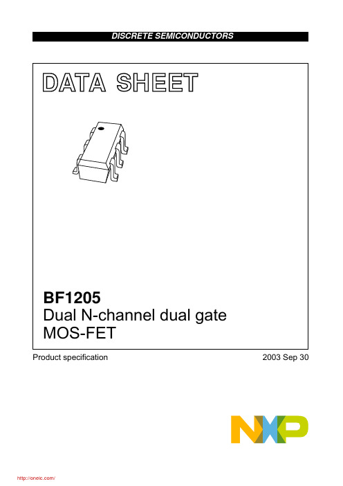
(1) ID (b); RG1 = 120 k. (2) ID (b); RG1 = 150 k. (3) ID (b); RG1 = 180 k.
(4) ID (a); RG1 = 180 k. (5) ID (a); RG1 = 150 k. (6) ID (a); RG1 = 120 k.
100
50
0 0 50 100 150 Ts (°C) 200
Fig.2 Power derating curve.
STATIC CHARACTERISTICS Tj = 25 C; per MOS-FET; unless otherwise specified. SYMBOL V(BR)DSS V(BR)G1-SS V(BR)G2-SS V(F)S-G1 V(F)S-G2 VG1-S(th) VG2-S(th) IDSX PARAMETER drain-source breakdown voltage gate-source breakdown voltage gate-source breakdown voltage forward source-gate voltage forward source-gate voltage gate-source threshold voltage gate-source threshold voltage drain-source current CONDITIONS MIN. MAX. 10 10 1.5 1.5 1 1.0 16 16 50 50 20 UNIT V V V V V V V V mA mA nA nA nA amp. a: VG1-S = VG2-S = 0 V; ID = 10 A 10 amp. b: VG1-S = VG2-S = 0 V; ID = 10 A 7 VGS = VDS = 0 V; IG1-S = 10 mA VGS = VDS = 0 V; IG2-S = 10 mA VG2-S = VDS = 0 V; IS-G1 = 10 mA VG1-S = VDS = 0 V; IS-G2 = 10 mA VDS = 5 V; VG2-S = 4 V; ID = 100 A VDS = 5 V; VG1-S = 5 V; ID = 100 A amp. a: VG2-S = 4 V; VDS = 5 V; RG1 = 150 k; note 1 amp. b: VG2-S = 4 V; VDS = 5 V; RG1 = 150 k; note 2 IG1-S IG2-S Note 1. RG1 connects gate 1 (b) to VGG = 0 V (see Fig.4). 2. RG1 connects gate 1 (b) to VGG = 5 V (see Fig.4). gate cut-off current gate cut-off current amp. a: VG1-S = 5 V; VG2-S = VDS = 0 V amp. b: VG1-S = 5 V; VG2-S = VDS = 0 V VG2-S = 4 V; VG1-S = VDS = 0 V 6 6 0.5 0.5 0.3 0.4 8 8
PZU5.1BA,115;PZU24BA,115;PZU6.2B2A,115;PZU7.5B3A,115;PZU3.9B1A,115;中文规格书,Datasheet资料
1.Product profile1.1General descriptionGeneral-purpose Zener diodes in a SOD323(SC-76) very small Surface-Mounted Device (SMD) plastic package.1.2Features1.3ApplicationsI General regulation functions1.4Quick reference data[1]Pulse test: t p ≤300µs;δ≤0.02.[2]t p =100µs; square wave; T j =25°C prior to surge[3]Device mounted on an FR4Printed-Circuit Board (PCB), single-sided copper, tin-plated and standard footprint.PZUxBA seriesSingle Zener diodesRev. 01 — 19 September 2008Product data sheetI Non-repetitive peak reverse power dissipation: P ZSM ≤40WI Low reverse current I R range I Total power dissipation: P tot ≤320mW I Small plastic package suitable for surface-mounted design I T olerance series:B:approximately ±5%;B1,B2,B3:approximately ±2%I AEC-Q101 qualifiedI Wide working voltage range:nominal 2.4V to 36V (E24range)Table 1.Quick reference data Symbol Parameter Conditions Min Typ Max Unit V F forward voltageI F =100mA[1]-- 1.1V P ZSM non-repetitive peak reverse power dissipation [2]--40W P tottotal power dissipationT amb ≤25°C [3]--320mW2.Pinning information[1]The marking bar indicates the cathode.3.Ordering information[1]The series consists of 97types with nominal working voltages from 2.4V to 36V .[2]/DG: halogen-freeTable 2.PinningPin Description Simplified outlineGraphic symbol1cathode [1]2anode21006aaa15221Table 3.Ordering informationType numberPackage NameDescriptionVersion PZU2.4BA to PZU36BA [1]SC-76plastic surface-mounted package; 2leadsSOD323PZU2.4BA/DG to PZU36BA/DG [1][2]4.MarkingTable 4.Marking codesType number[1]Marking code Type number[1]Marking codeB B1B2B3B B1B2B3PZU2.4*A X8---PZU2.4*A/DG Y8---PZU2.7*A X9XA XB-PZU2.7*A/DG Y9YA YB-PZU3.0*A XT XU XV-PZU3.0*A/DG YT YU YV-PZU3.3*A XW XX XY-PZU3.3*A/DG YW YX YY-PZU3.6*A XZ MC MD-PZU3.6*A/DG YZ NC ND-PZU3.9*A ME MF MG-PZU3.9*A/DG NE NF NG-PZU4.3*A MM MN MP MR PZU4.3*A/DG NM NN NP NRPZU4.7*A MS MT MU MV PZU4.7*A/DG NS NT NU NVPZU5.1*A MW MX MY MZ PZU5.1*A/DG NW NX NY NZPZU5.6*A LF LG LH LK PZU5.6*A/DG RF RG RH RKPZU6.2*A LL LM LN LP PZU6.2*A/DG RL RM RN RPPZU6.8*A LR LS LT LU PZU6.8*A/DG RR RS RT RUPZU7.5*A LV LW LX L Y PZU7.5*A/DG RV RW RX RYPZU8.2*A LZ CR CS CT PZU8.2*A/DG RZ ER ES ETPZU9.1*A CU CV CW CX PZU9.1*A/DG EU EV EW EXPZU10*A VA VB VC VD PZU10*A/DG WA WB WC WDPZU11*A VE VF VG VH PZU11*A/DG WE WF WG WHPZU12*A VK VL VM VN PZU12*A/DG WK WL WM WNPZU13*A VP VR VS VT PZU13*A/DG WP WR WS WTPZU14*A--VU-PZU14*A/DG--WU-PZU15*A VV VW VX VY PZU15*A/DG WV WW WX WYPZU16*A VZ X1X2X3PZU16*A/DG WZ Y1Y2Y3PZU18*A X4X5X6X7PZU18*A/DG Y4Y5Y6Y7PZU20*A XC XD XE XF PZU20*A/DG YC YD YE YFPZU22*A XG XH XK XL PZU22*A/DG YG YH YK YLPZU24*A XM XN XP XR PZU24*A/DG YM YN YP YRPZU27*A XS---PZU27*A/DG YS---PZU30*A MH---PZU30*A/DG NH---PZU33*A MK---PZU33*A/DG NK---PZU36*A ML---PZU36*A/DG NL---[1]* = B: tolerance series B, approximately±5%* = B1, B2, B3: tolerance series B1, B2, B3: approximately±2%5.Limiting values[1]t p =100µs; square wave; T j =25°C prior to surge[2]Device mounted on an FR4PCB, single-sided copper, tin-plated and standard footprint.[3]Device mounted on an FR4PCB, single-sided copper, tin-plated, mounting pad for cathode 1cm 2.6.Thermal characteristics[1]Device mounted on an FR4PCB, single-sided copper, tin-plated and standard footprint.[2]Device mounted on an FR4PCB, single-sided copper, tin-plated, mounting pad for cathode 1cm 2.[3]Soldering point of cathode tab.7.Characteristics[1]Pulse test: t p ≤300µs;δ≤0.02.Table 5.Limiting valuesIn accordance with the Absolute Maximum Rating System (IEC 60134).Symbol Parameter Conditions Min Max Unit I F forward current-200mAI ZSMnon-repetitive peak reverse current[1]-see Table 8and 9P ZSM non-repetitive peak reverse power dissipation [1]-40W P tot total power dissipation T amb ≤25°C[2]-320mW [3]-490mW T j junction temperature -150°C T amb ambient temperature −55+150°C T stgstorage temperature−65+150°CTable 6.Thermal characteristics Symbol ParameterConditions Min Typ Max Unit R th(j-a)thermal resistance from junction to ambient in free air[1]--390K/W [2]--255K/W R th(j-sp)thermal resistance from junction to solder point[3]--55K/WTable 7.CharacteristicsT j =25°C unless otherwise specified.Symbol Parameter ConditionsMin Typ Max Unit V Fforward voltage[1]I F =10mA --0.9V I F =100mA--1.1V[1]f =1MHz; V R =0V[2]t p =100µs; square wave; T j =25°C prior to surgeTable 8.Characteristics per type; PZU2.4BA to PZU5.6B3A and PZU2.4BA/DG to PZU5.6B3A/DG T j =25°C unless otherwise specified.PZUxBASelWorking voltage V Z (V)Differential resistance r dif (Ω)Reverse currentI R (µA)Temperature coefficient S Z (mV/K)Diode capacitance C d (pF)[1]Non-repetitivepeak reverse current I ZSM (A)[2]I Z =5mA I Z =0.5mA I Z =5mA I Z =5mA MinMax Max Max Max V R (V)Typ Max Max 2.4B 2.3 2.61000100501−1.645082.7B 2.5 2.91000100201−2.04408B1 2.5 2.75B22.65 2.93.0B 2.8 3.2100095101−2.14258B1 2.8 3.05B22.953.23.3B 3.1 3.510009551−2.44108B1 3.1 3.35B23.25 3.53.6B 3.4 3.810009051−2.43908B1 3.4 3.65B23.55 3.83.9B 3.7 4.110009031−2.53708B1 3.7 3.97B23.874.104.3B 4.01 4.4810009031−2.53508B1 4.01 4.21B2 4.15 4.34B34.28 4.484.7B 4.42 4.98008021−1.43258B1 4.42 4.61B2 4.55 4.75B34.69 4.95.1B 4.84 5.37250602 1.50.3300 5.5B1 4.84 5.04B2 4.98 5.2B35.14 5.375.6B 5.31 5.92100401 2.5 1.9275 5.5B1 5.31 5.55B2 5.49 5.73B35.675.92Table 9.Characteristics per type; PZU6.2BA to PZU36BA and PZU6.2BA/DG to PZU36BA/DG T j=25°C unless otherwise specified.PZUxBA Sel WorkingvoltageV Z(V)Differential resistancer dif(Ω)ReversecurrentI R(nA)TemperaturecoefficientS Z(mV/K)DiodecapacitanceC d(pF)[1]Non-repetitivepeak reversecurrentI ZSM(A)[2]I Z=5mA I Z=0.5mA I Z=5mA I Z=5mAMin Max Max Max Max V R(V)Typ Max Max 6.2B 5.86 6.5380305003 2.7250 5.5B1 5.86 6.12B2 6.06 6.33B3 6.26 6.536.8B 6.477.146020500 3.5 3.4215 5.5B1 6.47 6.73B2 6.65 6.93B3 6.867.147.5B7.067.8460105004 4.0170 3.5B17.067.36B27.287.60B37.527.848.2B7.768.6460105005 4.6150 3.5B17.768.1B28.028.36B38.288.649.1B8.569.5560105006 5.5120 3.5B18.568.93B28.859.23B39.159.5510B9.4510.5560101007 6.4110 3.5 B19.459.87B29.7710.21B310.1110.5511B10.4411.56601010087.41083 B110.4410.88B210.7611.22B311.111.5612B11.4212.6801010098.41053 B111.4211.9B211.7412.24B312.0812.613B12.4713.968010100109.4103 2.5 B112.4713.03B212.9113.49B313.3713.96[1]f =1MHz; V R =0V[2]t p =100µs; square wave; T j =25°C prior to surge14B213.7014.3080101001110.4101215B 13.8415.528015501111.4992B113.8414.46B214.3414.98B314.8515.5216B 15.3717.098020501212.497 1.5B115.3716.01B215.8516.51B316.3517.0918B 16.9419.038020501314.493 1.5B116.9417.7B217.5618.35B318.2119.0320B 18.8621.0810020501516.488 1.5B118.8619.7B219.5220.39B320.2121.0822B 20.8823.1710025501718.484 1.3B120.8821.77B221.5422.47B322.2323.1724B 22.9325.5712030501920.480 1.3B122.9323.96B223.7224.78B324.5425.5727B 25.128.915040502123.473130B 283220040502326.666133B 313525*********.7600.936B343830060502733.0590.8Table 9.Characteristics per type; PZU6.2BA to PZU36BA and PZU6.2BA/DG to PZU36BA/DG …continued T j =25°C unless otherwise specified.PZUxBASelWorking voltage V Z (V)Differential resistance r dif (Ω)Reverse currentI R (nA)Temperature coefficient S Z (mV/K)Diode capacitance C d (pF)[1]Non-repetitivepeak reverse current I ZSM (A)[2]I Z =5mA I Z =0.5mA I Z =5mA I Z =5mA MinMaxMaxMax Max V R (V)Typ Max MaxT j =25°C (prior to surge)T j =25°CFig 1.Non-repetitive peak reverse power dissipation as a function of pulse duration; maximum valuesFig 2.Forward current as a function of forward voltage; typical valuesT j =25°C to 150°C V Z =2.4V to 4.3VT j =25°C to 150°C V Z =4.7V to 12VFig 3.Temperature coefficient as a function of working current; typical valuesFig 4.Temperature coefficient as a function of working current; typical values006aab21510210103P ZSM (W)1t p (s)10−410−210−3V F (V)0.610.8mbg781100200300I F (mA)00600−2−3−1mgl2732040I Z (mA)S Z (mV/K)4.33.93.63.33.02.42.702016100−55mgl2744812I Z (mA)S Z (mV/K)4.71211109.18.27.56.86.25.65.1T j =25°C V Z =2.4V to 4.3VT j =25°C V Z =4.7V to 12VFig 5.Working current as a function of working voltage; typical valuesFig 6.Working current as a function of working voltage; typical valuesT j =25°C V Z =13V to 36VFig 7.Working current as a function of working voltage; typical values006aab24610−110−2101102I Z (mA)10−3V Z (V)054231V Z(nom) (V) = 2.42.73.03.33.63.94.3006aab24710−110−2101102I Z (mA)10−3V Z (V)01410128624V Z(nom) (V) = 4.75.15.66.26.87.58.29.1101112006aab24810−110−2101102I Z (mA)10−3V Z (V)10403020V Z(nom) (V) = 1318202224273033361415168.Test information8.1Quality informationThis product has been qualified in accordance with the Automotive Electronics Council (AEC) standard Q101 - Stress test qualification for discrete semiconductors , and is suitable for use in automotive applications.9.Package outline10.Packing information[1]For further information and the availability of packing methods, see Section 13.Fig 8.Package outline SOD323(SC-76)03-12-17Dimensions in mm0.250.100.450.152.72.3 1.81.60.400.251.10.81.351.1512Table 10.Packing methodsThe indicated -xxx are the last three digits of the 12NC ordering code.[1]Type number Package DescriptionPacking quantity 300010000PZU2.4BA to PZU36BA SOD3234mm pitch, 8mm tape and reel-115-135PZU2.4BA/DG to PZU36BA/DG分销商库存信息:NXPPZU5.1BA,115PZU24BA,115PZU6.2B2A,115 PZU7.5B3A,115PZU3.9B1A,115PZU20B1A,115 PZU10BA,115PZU11BA,115PZU12BA,115 PZU13BA,115PZU15BA,115PZU16BA,115 PZU18BA,115PZU2.4BA,115PZU2.7BA,115 PZU20BA,115PZU22BA,115PZU27BA,115 PZU3.0BA,115PZU3.3BA,115PZU3.6BA,115 PZU3.9BA,115PZU30BA,115PZU33BA,115 PZU36BA,115PZU4.3BA,115PZU4.7BA,115 PZU5.6BA,115PZU6.2BA,115PZU6.8BA,115 PZU5.1B1A,115PZU10B1A,115PZU10B2A,115 PZU10B3A,115PZU11B1A,115PZU11B2A,115 PZU11B3A,115PZU12B1A,115PZU12B2A,115 PZU12B3A,115PZU13B1A,115PZU13B2A,115 PZU13B3A,115PZU14B2A,115PZU15B1A,115 PZU15B2A,115PZU15B3A,115PZU16B1A,115 PZU16B2A,115PZU16B3A,115PZU18B1A,115 PZU18B2A,115PZU18B3A,115PZU2.7B1A,115 PZU2.7B2A,115PZU20B2A,115PZU20B3A,115 PZU22B1A,115PZU22B2A,115PZU22B3A,115 PZU24B1A,115PZU24B2A,115PZU24B3A,115 PZU3.0B1A,115PZU3.0B2A,115PZU3.3B1A,115 PZU3.3B2A,115PZU3.6B1A,115PZU3.6B2A,115 PZU4.3B1A,115PZU8.2B1A,115PZU8.2B2A,115。
bh1750FVI 中文数据手册
实例 2. 重置集成电路的应用 1. “推拉式”重置 IC
2. 打开重置 IC 的漏极输出 实例 3. 另一种供电模式
※DVI 提供电源标准应低于 VCC 提供电源标准,以保证重置区正常(≥1us)。
连续测量 通过 I2C 写指令 自动状态转换
2010.04 - Rev.C
BH1750FVI
Technical Note
指令集合结构
指令
功能代码
注释
断电
0000_0000
无激活状态。
通电
0000_0001
等待测量指令。
重置
0000_0111
重置数字寄存器值,重置指令在断电模式下 不起作用。
连续 H 分辨率模式
一次 H 分辨率模式
0010_0000
测量时间一般为 120ms。
测量后自动设置为断电模式。
在 0.5lx 分辨率下开始测量。
一次 H 分辨率模式 2
0010_0001
测量时间一般为 120ms。
测量后自动设置为断电模式。
在 41lx 分辨率下开始测量。
一次 L 分辨率模式
0010_0011
测量时间一般为 16ms。
7 / 17
© 2010 ROHM Co., Ltd. All rights reserved.
2010.04 - Rev.C
BH1750FVI
Technical Note
DVI终端应用电路实例
DVI 终端是一个异步重置终端。请注意,如果在启动连接 VCC 完毕后没有设置重置区, 可能导致集成电路不正常运行。(请参阅“DVI 和 VCC 电源供应时序图”) 这下面描述中的应用电路实例中,省略了 SDA 和 SCL 和终端。在设计时,请设计满足 I2C 总线标准以便达到理想状态。此外,实例还省略了 ADDR 终端设计因素,在进行 ADDR 终端设计时,请参阅“DVI 和 VCC 电源供应时序图”。 实例 1. 连接控制信号线(如:CPU)
PCA21125TQ9001,1;中文规格书,Datasheet资料

PCA21125SPI-bus Real-Time Clock and calendarRev. 01 — 16 November 2009Product data sheet1.General descriptionThe PCA21125 is a CMOS1 Real-Time Clock (RTC) and calendar optimized for low-powerconsumption and an operating temperature up to 125 °C. Data is transferred via a SerialPeripheral Interface (SPI-bus) with a maximum data rate of 6.0 Mbit/s. Alarm and timerfunctions are also available with the possibility to generate a wake-up signal on theinterrupt pin.AEC Q100 compliant for automotive applications.2.FeaturesProvides year, month, day, weekday, hours, minutes, and seconds based on32.768 kHz quartz crystalResolution: seconds to yearsClock operating voltage: 1.3 V to 5.5 VLow backup current: typical 0.55 μA at V DD = 3.0 V and T amb = 25 °C3-line SPI-bus with separate, but combinable data input and outputSerial interface at V DD = 1.6 V to 5.5 V1 second or 1 minute interrupt outputFreely programmable timer with interrupt capabilityFreely programmable alarm function with interrupt capabilityIntegrated oscillator capacitorsInternal Power-On Reset (POR)Open-drain interrupt pin3.ApplicationsAutomotive time keepingMetering1.The definition of the abbreviations and acronyms used in this data sheet can be found in Section 17.4.Ordering informationTable 1.Ordering informationType number Package NameDescriptionVersionPCA21125T/Q900/1TSSOP14plastic thin shrink small outline package; 14 leads; body width 4.4 mmSOT402-15.MarkingTable 2.Marking codesType number Marking code PCA21125T/Q900/1PC211256.Block diagram7.Pinning information7.1Pinning7.2Pin descriptionTable 3.Pin descriptionSymbol Pin DescriptionOSCI1oscillator inputOSCO2oscillator outputn.c.3, 4not connected; do not connect and do not use as feed through; connectto V DD if floating pins are not allowedINT5interrupt output (open-drain; active LOW)CE6chip enable input (active HIGH) with 200 kΩ pull-down resistorV SS7ground supply voltageSDO8serial data output, push-pullSDI9serial data input; might float when CE inactiveSCL10serial clock input; might float when CE inactiven.c.11, 12not connected; do not connect and do not use as feed through; connectto V DD if floating pins are not allowedCLKOUT13clock output (open-drain)V DD14supply voltage8.Functional descriptionThe PCA21125 contains 16 8-bit registers with an auto-incrementing address register, anon-chip 32.768 kHz oscillator with one integrated capacitor, a frequency divider whichprovides the source clock for the RTC, a programmable clock output, and a 6 MHzSPI-bus.All 16 registers are designed as addressable 8-bit parallel registers although not all bitsare implemented:•The first two registers at addresses 00h and 01h (Control_1 and Control_2) are used as control and status registers.•Registers at addresses 02h to 08h (Seconds, Minutes, Hours, Days, Weekdays,Months, Years) are used as counters for the clock function. Seconds, minutes, hours,days, months, and years are all coded in Binary Coded Decimal (BCD) format. Whenone of the RTC registers is read the contents of all counters are frozen. Therefore,faulty reading of time and date during a carry condition is prevented.•Registers at addresses 09h to 0Ch (Minute_alarm, Hour_alarm, Day_alarm, andWeekday_alarm) define the alarm condition.•The register at address 0Dh (CLKOUT_control) defines the clock output mode.•Registers at addresses 0Eh and 0Fh (Timer_control and Countdown_timer) are used for the countdown timer function. The countdown timer has four selectable sourceclocks allowing for countdown periods in the range from less than 1 ms to more than4 hours (see Table 29). There are also two pre-defined timers which can be used togenerate an interrupt once per second or once per minute. These are defined inregister Control_2 (01h).8.1Register overviewThe time, date, and alarm registers are encoded in BCD to simplify application use. Otherregisters are either bit-wise or standard binary.Table 4.Register overviewBits labeled - are not implemented and will return logic 0 when read. Bit positions labeled N should always be written with logic 0. After reset, all registers are set according to Table 37.Address Register name Bit76543210Control and status registers00h Control_1EXT_TEST N STOP N POR_OVRD12_24N N01h Control_2MI SI MSF TI_TP AF TF AIE TIETime and date registers02h Seconds RF SECONDS (0 to 59)03h Minutes-MINUTES (0 to 59)04h Hours--AMPM HOURS (1 to 12) in 12 hour mode--HOURS (0 to 23) in 24 hour mode05h Days--DAYS (1 to 31)06h Weekdays-----WEEKDAYS (0 to 6)07h Months---MONTHS (1 to 12)08h Years YEARS (0 to 99)Alarm registers09h Minute_alarm AE_M MINUTE_ALARM (0 to 59)0Ah Hour_alarm AE_H-AMPM HOUR_ALARM (1 to 12) in 12 hour mode-HOUR_ALARM (0 to 23) in 24 hour mode0Bh Day_alarm AE_D-DAY_ALARM (1 to 31)0Ch Weekday_alarm AE_W----WEEKDAY_ALARM (0 to 6) CLKOUT control register0Dh CLKOUT_control-----COFTimer registers0Eh Timer_control TE-----CTD0Fh Countdown_timer COUNTDOWN_TIMER8.2Control and status registers8.2.1Register Control_1Table 5.Control_1 - control and status register 1 (address 00h) bit descriptionBit Symbol Value Description Reference7EXT_TEST0[1]normal mode Section 8.81external clock test mode6N0unused-5STOP0[1]RTC source clock runs Section 8.91RTC clock is stopped[2]4N0unused-3POR_OVRD0POR override facility is disabled;Section 8.10.1Remark: set logic 0 for normal operation1[1]POR override enabled212_240[1]24 hour mode selected Table 10 and Table 18112 hour mode selected1 to 0N0unused-[1]Default value.[2]CLKOUT at 32.768 kHz, 16.384 kHz or 8.192 kHz is still available; divider chain flip-flops are asynchronously set logic 0.8.2.2Register Control_2Table 6.Control_2 - control and status register 2 (address 01h) bit descriptionBit Symbol Value Description Reference7MI0[1]minute interrupt disabled Section 8.6.11minute interrupt enabled6SI0[1]second interrupt disabled Section 8.6.11second interrupt enabled5MSF0[1]no minute or second interrupt generated Section 8.6.11flag set when minute or second interrupt generated4TI_TP0[1]interrupt pin follows TF and MSF (see Figure 9)Section 8.6 et seqq. andSection 8.7 et seqq.1interrupt pin generates a pulse3AF0[1]no alarm interrupt generated Section 8.4.51flag set when alarm triggered;Remark: flag must be cleared to clear interrupt2TF0[1]no countdown timer interrupt generated Section 8.6 et seqq. andSection 8.7 et seqq.1flag set when countdown timer interrupt generated1AIE0[1]no interrupt generated from alarm flag Section 8.7.31interrupt generated when alarm flag set0TIE0[1]no interrupt generated from countdown timer flag Section 8.71interrupt generated when countdown timer flag set[1]Default value.8.3Time and date registersThe majority of these registers are coded in the Binary Coded Decimal (BCD) format.BCD is used to simplify application use. An example is shown for register Seconds inTable 8.Loading these registers with values outside of the given range will result in unpredictable time and date generation (see Figure 3 “Data flow of the time function”).8.3.1Register SecondsTable 7.Seconds - seconds and clock integrity status register (address 02h) bitdescriptionBit Symbol Value Description7RF0clock integrity is guaranteed1[1]clock integrity is not guaranteed;chip reset has occurred since flag was last cleared6 to 4SECONDS0 to 5ten’s place3 to 00 to 9unit place[1]Start-up value.Table 8.Seconds coded in BCD formatSeconds value in decimal Upper-digit (ten’s place)Digit (unit place)Bit 6Bit 5Bit 4Bit 3Bit 2Bit 1Bit 0000000000 010000001 020000010 :::::::: 090001001 100010000 :::::::: 581011000 5910110018.3.2Register MinutesTable 9.Minutes - minutes register (address 03h) bit descriptionBit Symbol Value Description7-0unused6 to 4MINUTES0 to 5ten’s place3 to 00 to 9unit place8.3.3Register HoursTable 10.Hours - hours register (address 04h) bit descriptionBit Symbol Value Description7 to 6-0unused12 hour mode[1]5AMPM0indicates AM1indicates PM4 to 0HOURS0 to 1ten’s place3 to 00 to 9unit place24 hour mode[1]5 to 4HOURS0 to 2ten’s place3 to 00 to 9unit place[1]Hour mode is set by bit 12_24 in register Control_1 (see Table 5).8.3.4Register DaysTable 11.Days - days register (address 05h) bit descriptionBit Symbol Value Place value Description7 to 6---unused5 to 4DAYS[1]0 to 3ten’s place actual day coded in BCD format3 to 00 to 9unit place[1]The PCA21125 compensates for leap years by adding a 29th day to February if the year counter contains avalue which is exactly divisible by 4, including the year 00.8.3.5Register WeekdaysTable 12.Weekdays - weekdays register (address 06h) bit descriptionBit Symbol Value Description7 to 3--unused2 to 0WEEKDAYS0 to 6actual weekday, values see Table 13Table 13.Weekday assignmentsDay[1]Bit210Sunday000Monday001Tuesday010Wednesday011Thursday100Friday101Saturday110[1]Definition may be re-assigned by the user.8.3.6Register MonthsTable 14.Months - months register (address 07h) bit descriptionBit Symbol Value Description7 to 5-0unused4MONTHS0 to 1ten’s place3 to 00 to 9unit placeTable 15.Month assignments in BCD formatMonth Upper-digitDigit (unit place)(ten’s place)Bit 4Bit 3Bit 2Bit 1Bit 0 January00001February00010March00011April00100May00101June00110July00111August01000September01001October10000November10001December10010 8.3.7Register YearsTable 16.Years - years register (08h) bit descriptionBit Symbol Value Place value Description7 to 4YEARS0 to 9ten’s place actual year coded in BCD format3 to 00 to 9unit place8.3.8Setting and reading the timeFigure 3 shows the data flow and data dependencies starting from the 1 Hz clock tick.During read/write operations, the time counting circuits (memory locations 02h through08h) are blocked.This prevents•Faulty reading of the clock and calendar during a carry condition•Incrementing the time registers during the read cycleAfter this read/write access is completed, the time circuit is released again and anypending request to increment the time counters that occurred during the read/write access is serviced. A maximum of 1 request can be stored; therefore, all accesses must becompleted within 1 second (see Figure 4).As a consequence of this method, it is very important to make a read or write access inone go, that is, setting or reading seconds through to years should be made in one single access. Failing to comply with this method could result in the time becoming corrupted.分销商库存信息: NXPPCA21125T/Q900/1,1。
LSM303DLHTR;LSM303DLH;中文规格书,Datasheet资料
LGA-28L (5x5x1.0 mm)
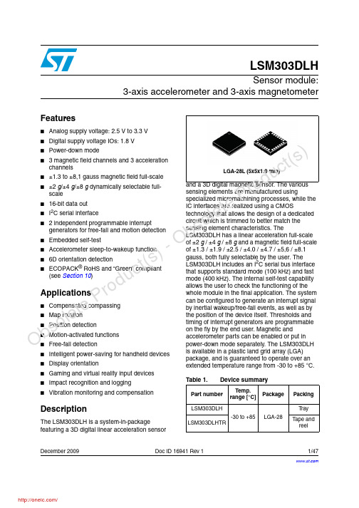
and a 3D digital magnetic sensor. The various sensing elements are manufactured using specialized micromachining processes, while the IC interfaces are realized using a CMOS technology that allows the design of a dedicated circuit which is trimmed to better match the sensing element characteristics. The LSM303DLH has a linear acceleration full-scale of ±2 g / ±4 g / ±8 g and a magnetic field full-scale of ±1.3 / ±1.9 / ±2.5 / ±4.0 / ±4.7 / ±5,6 / ±8.1 gauss, both fully selectable by the user. The LSM303DLH includes an I2C serial bus interface that supports standard mode (100 kHz) and fast mode (400 kHz). The internal self-test capability allows the user to check the functioning of the whole module in the final application. The system can be configured to generate an interrupt signal by inertial wakeup/free-fall events, as well as by the position of the device itself. Thresholds and timing of interrupt generators are programmable on the fly by the end user. Magnetic and accelerometer parts can be enabled or put in power-down mode separately. The LSM303DLH
IXBP5N160G;IXBH5N160G;中文规格书,Datasheet资料

Symbol RthCH Weight
Conditions with heatsink compound (TO-220) (TO-247)
Characteristic Values min. typ. max. 0.25 2 6 K/W g g
Dim. A B C D E F G H J K M N Q R Millimeter Min. Max. 12.70 13.97 14.73 16.00 9.91 10.66 3.54 4.08 5.85 6.85 2.54 3.18 1.15 1.65 2.79 5.84 0.64 1.01 2.54 BSC 4.32 4.82 1.14 1.39 0.35 0.56 2.29 2.79 Inches Min. Max. 0.500 0.550 0.580 0.630 0.390 0.420 0.139 0.161 0.230 0.270 0.100 0.125 0.045 0.065 0.110 0.230 0.025 0.040 0.100 BSC 0.170 0.190 0.045 0.055 0.014 0.022 0.090 0.110
High Voltage BIMOSFETTM
Monolithic Bipolar MOS Transistor
Preliminary data sheet
IXBP 5N160 G IXBH 5N160 G
IC25 VCES VCE(sat) tf
TO-220 AB
G C E
= 5.7 A = 1600 V = 4.9 V = 70 ns
VCE(sat) VGE(th) ICES IGES td(on) tr td(off) tf Cies QGon VF RthJC
BH产品规格书模板
音量增加
短按音量加键
/
/
在通话或音乐播放状态,按加键将 增加耳机音量,按着加键不放,可 快速增加音量。
Con diti on
指示灯
1
开机
蓝灯长亮1秒
2
配对
监灯、红灯交替闪烁
3
等连接
蓝灯每秒闪一下
4
待机
蓝灯2秒闪1下
8
低电
红灯有节奏快闪
9
充电中
红灯长亮
10
充电完成
红灯熄火
10)常规功能
功能
操作
LED状
态
提示音
功能详细描述
开机
关机状态,按住多功
能键3S
蓝灯每秒闪
一下
有提示音
.
关机
开机状态,按住多功
能键5S
NOMINAL
LIMIT
UNIT
a)
LOW BATTERY WARNING VOLTAGE
报警电压
3.5
3.45---3.55
V
b)
AUTO POWER OFF VOLTAGE
关机电压
3.3
2.25---3.35
V
6)CHARGE CURRENT (AT STANDARD INPUT VOLTAGE)充电电流测试
DESCRIPTION
NOMINAL
LIMIT
UNIT
a) ST-BY TIME待机时间
300
-
b)TALK TIME通话时间
8
-
H
c)MAX CHARGE TIME最大充电时间
连云港美华电子科技有限公司MHT194UGBCT LED SMD产品规格书说明书
连云港美华电子科技有限公司Lianyungang Meihua Electronics Technology Co.,Ltd产品规格书DATA SHEETPart No :MHT194UGBCTREV.1本产品符合ROHS 指令有关限制有害物质的环保要求.电 话传 真邮件E-mail:***************.cn 网 址Web:地址ADD:中国·江苏省连云港市灌南经济开发区北环路North Around Road,Guannan EDA,Lianyungang City,Jiangsu Province China.日期 DATE 拟制 PREPARED审核 VERIFIED批准 APPROVED 2020-03-24LiuSunny客户签回 CUSTOMER’S APPROVALP/N:MHT194UGBCT LED SMD 产品外观尺寸PACKAGE DIMENSIONS注意NOTES :1. 所有尺寸均为mm(英寸)All dimensions are in millimeters. (inches)2. 如无特殊说明,公差为0.10mm(0.004")Tolerance is ±0.10mm(0.004") unless otherwise specified.P/N:MHT194UGBCT LED SMD 产品特性FEATURES●高可靠性和高稳定性High intensity and reliability●与红外、气相回流焊工艺兼容Compatible with infrared and vapor phase reflow solder process●宽视角Wide viewing angle●符合RoHS指令要求ROHS COMPLIANC●无铅产品Pb FREE PRODUCTS产品特征Description●0605规格封装0605 package●顶部发光Top view LED●胶体颜色:透明Lens Color:Water Clear●发光颜色Emitted color:1.绿色: Green2.蓝色: Blue3.4.5.6.●晶片材质Chips materials:1.lnGaN2.InGaN3.4.5.6.P/N :MHT194UGBCTLED SMD极限参数Absolute Maximum Ratings(Ta=25℃)参数 Parameter 符号 Symbol 极限值 Rating单位 Unit 功耗Power Dissipation PAD G:100 mW B:100 最大峰值电流Peak Forward Current Per Segment (1/10 duty cycle ,1ms pulse width )IFP G:100 mA B:100 正向使用电流Continuous Forward CurrentIF G:25 mA B:25 反向电压 Reverse Voltage VR G:5 VB:5工作温度Operating Temperature RangeTOPR -40℃ to +85℃ 储藏温度Storage Temperature RangeTSTG-40℃ to +85℃P/N :MHT194UGBCTLED SMD光电特性Optical-Electrical Characteristic(Ta=25℃)Notes:1. 发光强度公差为±10%。
