HZS20-3L中文资料
汉昇HS12864B液晶显示模块使用说明书
HS12864B液晶显示模块使用说明书感谢您关注和使用我们的液晶产品。
如果您在使用中有任何疑问,请拨打我们的客户服务热线寻求技术支持和获取相关资料,我们竭诚为您服务。
您可以登录我们的网站了解最新产品信息。
或者您可以在我公司网站的留言簿栏目留下您宝贵的意见。
深圳汉昇实业有限公司SHENZHEN HANSHENG INDUSTRIAL CO.,LTD地址:深圳市南山区西丽镇官龙工业村东区18栋5楼邮编:518055公司主页:联系电话:传真:一、 概述HS12864B 使用KS0108(或其兼容芯片)作为控制器,适配M6800系列时序,具有8位标准数据总线。
可显示各种字符及图形。
每个KS0108拥有64×64位(512字节)的显示RAM ,HS12864B 显示屏上的64×64点,显示RAM 中的数据直接作为显示驱动信号。
HS12864B 具有操作指令简单,低功耗的特点。
HS12864B 采用COB 工艺制作。
说明:HS12864B 有STN 黄绿膜,蓝膜以及FSTN 产品可选,LED 背光有多种颜色可选。
用户还可以根据需要自己选定常温、宽温或者超宽温产品。
二、 外形结构1. 外形图2.114-?2. 主要外形尺寸项 目 标 准 尺 寸单 位模 块 体 积 93.0L ×70.0W ×13.0(max )H mm视 域 70.7×38.8 mm 行 列 点 阵 数 128×64 dots 点 距 离 0.48×0.48 mm 点 大 小0.52×0.52 mm三、 硬件说明1. 接口定义管脚符号电平功能描述1 CS1 L 片选信号1,低有效,对应左半屏64×64点2 CS2 L 片选信号2,低有效,对应右半屏64×64点与CSA,CSB不可同时使用3 VSS 0V 电源地4 VDD 5.0V 供电电源,5.0V5 V0 负压 LCD驱动电压输入端(对比度调节)6 RS H/L 寄存器选择端高:数据寄存器低:命令寄存器7 R/W H/L 读/写信号高:读操作低:写操作8 E H,H->L 使能信号9 ~16 DB0~DB7H/L 数据线17 CSA H 片选信号1,高有效,对应左半屏64×64点18 CSB H 片选信号2,高有效,对应右半屏64×64点与CS1,CS2不可同时使用19 /RST H/L 复位信号,低有效20 V out 负压负压输出端21 LEDA 5.0V 背光正极22 LEDK 0V 背光负极说明:HS12864B有两套片选信号,分别是CS1,CS2和CSA,CSB,分别是低有效和高有效,以适应不同用户的需求。
SHT3x中文资料简介
SHT3x中⽂资料简介Datasheet SHT3x-DIS Humidity and Temperature SensorSHT3x-DIS湿度和温度传感器说明书Fully calibrated, linearized, and temperature compensated digital output.完全校准,线性化和温度补偿的数字输出。
Wide supply voltage range, from 2.4 V to 5.5 V.宽电源电压范围:2.4 V⾄5.5V。
I2C Interface with communication speeds up to 1 MHz and two user selectable addresses.I2C接⼝,通信速度⾼达1 MHz,并且具有两个⽤户可选地址。
Typical accuracy of 1.5 %RH and 0.1 °C for SHT35.SHT35的典型精度为1.5%RH和0.1°C。
Very fast start-up and measurement time.快速的启动和测量时间。
Tiny 8-Pin DFN package.Tiny 8引脚DFN封装。
Product Summary产品概要SHT3x-DIS是Sensirion的下⼀代温度和湿度传感器。
它基于新的CMOSens?传感器芯⽚,该芯⽚是Sensirion新型湿度和温度平台的核⼼。
与之前的产品相⽐,SHT3x-DIS具有更⾼的智能性,可靠性和更⾼的精度指标。
它的功能包括增强的信号处理,两个独特的、可选的I2C地址以及⾼达1 MHz的通信速度。
DFN封装的尺⼨为2.5 x 2.5 mm2,同时保持0.9 mm的⾼度。
这允许将SHT3x-DIS集成到各种各样的应⽤程序中。
此外,2.4 V⾄5.5 V的宽电源电压范围确保了与各种组装情况的兼容性。
总⽽⾔之,SHT3x-DIS融合了15年的湿度传感器⾏业领导者Sensirion的知识。
3590S-2-502L;3590S-2-102L;3590S-2-103L;3590S-2-203L;3590S-1-502L;中文规格书,Datasheet资料

Specifi cations are subject to change without notice.Customers should verify actual device performance in their specifi c applications.*RoHS Directive 2002/95/EC Jan. 27, 2003 including annex and RoHS Recast 2011/65/EU June 8, 2011.Stop Strength..............................................................................................................................................................................45 N-cm (64 oz.-in.) minimum Mechanical Angle ...........................................................................................................................................................................................3600 ° +10 °, -0 °Torque (Starting & Running) ................................................................................................................................0.35 N-cm (0.5 oz.-in.) maximum (unsealed) 1.1 N-cm (1.5 oz.-in.) maximum (sealed) Mounting ..............................................................................................................................................................................55-80 N-cm (5-7 lb.-in.) (plastic) 90-113 N-cm (8-10 in.-lb.) (metal)Shaft Runout......................................................................................................................................................................................0.13 mm (0.005 in.) teral Runout ...................................................................................................................................................................................0.20 mm (0.008 in.) T.I.R.Shaft End Play ...................................................................................................................................................................................0.25 mm (0.010 in.) T.I.R.Shaft Radial Play ...............................................................................................................................................................................0.13 mm (0.005 in.) T.I.R.Pilot Diameter Runout .......................................................................................................................................................................0.08 mm (0.003 in.) T.I.R.Backlash ............................................................................................................................................................................................................1.0 ° maximum Weight ........................................................................................................................................................................................................Approximately 19 G Terminals ................................................................................................................................................................................................Solder lugs or PC pins Soldering ConditionManual Soldering...........................................................96.5Sn/3.0Ag/0.5Cu solid wire or no-clean rosin cored wire; 370 °C (700 °F) max. for 3 seconds Wave Soldering ...................................................................................96.5Sn/3.0Ag/0.5Cu solder with no-clean fl ux; 260 °C (500 °F) max. for 5 seconds Wash processes .......................................................................................................................................................................................Not recommended Marking .....................................Manufacturer’s name and part number, resistance value and tolerance, linearity tolerance, wiring diagram, and date code.Ganging (Multiple Section Potentiometers) ......................................................................................................................................................1 cup maximum Hardware ............................................................................................................One lockwasher and one mounting nut is shipped with each potentiometer.NOTE: For Anti-rotation pin add 91 after confi guration dash number. Example: -2 becomes -291 to add AR pin.1At room ambient: +25 °C nominal and 50 % relative humidity nominal, except as noted. 2Consult manufacturer for complete specifi cation details for resistances below 1k ohms.BOLDFACE LISTINGS ARE IN STOCK AND READILY AVAILABLETHROUGH DISTRIBUTION. FOR OTHER OPTIONS CONSULT FACTORY.ROHS IDENTIFIER: L = COMPLIANTRecommended Part Numbers(Printed Circuit)(Solder Lug)(Solder Lug)Resistance (Ω)Resolution (%)3590P-2-102L 3590S-2-102L 3590S-1-102L 1,000.0293590P-2-202L 3590S-2-202L 3590S-1-202L 2,000.0233590P-2-502L 3590S-2-502L 3590S-1-502L 5,000.0253590P-2-103L 3590S-2-103L 3590S-1-103L 10,000.0203590P-2-203L 3590S-2-203L 3590S-1-203L 20,000.0193590P-2-503L 3590S-2-503L 3590S-1-503L 50,000.0133590P-2-104L3590S-2-104L3590S-1-104L100,000.009*Ro H S C O MP L I A N T/Panel Thickness Dimensions(For Bushing Mount Only)1.60 +.08/-.03(.063 +.003/-.001)DIA.ANTI-ROTATION PINAnti-rotation pin hole is shown at six o'clockposition for reference only. The actual location isdetermined by the customer's application. Referto the front view of the potentiometer to see thelocation of the optional A/R pin.Panel thickness and hole diameters arerecommended for best fit. However, customersmay adjust the dimensions to suit their specificapplication.Product DimensionsSpecifi cations are subject to change without notice.Customers should verify actual device performance in their specifi c applications.REV. 06/12 MOUNTING SURFACE-2, -4, -6, -8 Confi gurations-1, -3, -5, -7 Confi gurationsRecommended PCB LayoutHOLE DIAMETER5.08(.200)5.08(.200)6.99(.275)SchematicTOLERANCES: EXCEPT WHERE NOTED.508 .127DECIMALS: .XX ±(.02),.XXX ±(.005)FRACTIONS: ±1/64MMDIMENSIONS:(IN.)Shaft & Bushing Confi gurations(Bushing - DxL, Shaft - D):(-1) Plastic Bushing (3/8 ” x 5/16 ”)and Shaft (.2480 + .001, - .002)(-2) Metal Bushing (3/8 ” x 5/16 ”)and Shaft (.2497 + .0000, - .0009)(-3) Sealed, Plastic Bushing (3/8 ” x 5/16 ”)and Shaft (.2480 + .001, - .002)(-4) Sealed, Metal Bushing (3/8 ” x 5/16 ”)and Shaft (.2497 + .0000, - .0009)(-5) Metric, Plastic Bushing (9 mm x 7.94 mm)and Shaft (6 mm + 0, - .076 mm)(-6) Metric, Metal Bushing (9 mm x 7.94 mm)and Shaft (6 mm + 0, - .023 mm)(-7) Metric, Sealed, Plastic Bushing (9 mm x7.94 mm) and Shaft (6 mm + 0, - .076 mm)(-8) Metric, Sealed, Metal Bushing (9 mm x7.94 mm) and Shaft (6 mm + 0, - .023 mm)Terminal Styles“P” Terminal Style“S” Terminal Style/分销商库存信息:BOURNS3590S-2-502L3590S-2-102L3590S-2-103L 3590S-2-203L3590S-1-502L3590S-2-104L 3590S-1-203L3590S-2-501L3590S-2-202L 3590S-1-503L3590S-2-503L3590S-1-104L 3590S-291-102L3590S-291-203L3590S-291-502L 3590S-1-201L3590S-1-501L3590S-2-101L 3590S-2-201L3590P-1-102L3590P-1-103L 3590P-1-201L3590P-1-502L3590S-1-102L 3590S-1-103L3590S-2-252L3590P-291-501L 3590P-2-102L3590P-2-201L3590P-2-203L 3590P-2-502L3590S-1-202L3590S-6-102L 3590S-6-201L3590S-6-202L3590S-6-203L 3590S-6-501L3590P-1-104L3590S-6-502L 3590S-4-102L3590S-4-103L3590S-4-202L 3590S-4-203L3590S-4-502L3590S-8-102L 3590S-8-103L3590S-8-202L3590P-2-104L 3590P-4-103L3590P-4-202L3590S-6-503L 3590S-6-104L3590S-4-104L3590P-4-503L 3590P-4-104L3590S-2-5023590S-1-102 3590S-1-1033590S-1-1043590S-1-203 3590S-1-5023590S-1-5033590S-2-102 3590S-2-1033590S-2-1043590S-2-203 3590S-2-5033590S-1-2023590S-2-202 3590S-2-501。
深圳市华盛 HS1085说明书
HS1085-2.5,
IOUT=10mA, VIN=5.5V 10mA≤IOUT≤3A, 2.462 2.5 2.537
V
VOUT
4.0V≤VIN ≤7V HS1085-3.3,
2.45
2.5
2.55
IOUT=10mA, VIN=6.3V, 10mA≤IOUT≤3A, 3.225 3.3 3.350
版本号:1.3 共 12 页 第 2 页
深圳市华盛电子科技有限公司
产品名称 HS1085S2-1.5 HS1085S2-1.5TR HS1085S2-1.8 HS1085S2-1.8TR HS1085S2-2.5 HS1085S2-2.5TR HS1085S2-3.3 HS1085S2-3.3TR HS1085S2-5.0 HS1085S2-5.0TR
11.88 12.00 12.12 V
11.76 12.00 12.24
HS1085-ADJ, IOUT=10mA, 2.85V≤VIN≤10V
0.035 0.2
%
HS1085-1.5, IOUT=10mA, 3.0V≤VIN≤10V
1
6
mV
HS1085-1.8, ∆VOUT
IOUT=10mA, 3.3V≤VIN≤10V
内部框图
封装形式
打印名称 HS1085S2-1.5 HS1085S2-1.5 HS1085S2-1.8 HS1085S2-1.8 HS1085S2-2.5 HS1085S2-2.5 HS1085S2-3.3 HS1085S2-3.3 HS1085S2-5.0 HS1085S2-5.0
VIN
HS1085 说明书
封装形式 TO-252-2L
TO-263-3L TO-220-3L TO-263-2L
ZL30310GKG中文资料(microsemi)中文数据手册「EasyDatasheet - 矽搜」
传统PLL行为,再加上数据包时间服务器, 例如,结合同步以太网和IEEE1588服务器
客户端行为, 例如,IEEE1588客户端
传统PLL行为,再加上数据包时客户端, 无论是作为故障转移从一个到另一个,或组合 例如,结合同步以太网和IEEE 1588客户端
• 支持故障防护持如果服务器流丢失 • 接受八个输入引用,以及多达三个
相关低频对齐或成帧脉冲
• 生成多达四个独立输出时钟 8千赫至100兆赫之间频率
结合同步以太网和
IEEE1588网络同步
ZL30310
数据表
June 2009
ZL30310GKG ZL30310GKG2
256 TEPBGA,17×17毫米 256 TEPBGA,17×17毫米
ISSUE
1
2
ACN
CDCA
日期
24Aug06
APPRD.Leabharlann 上一页封装代码封装编码
芯片中文手册,看全文,戳
Information relating to productsand servicesfurnished herein by ZarlinkSemiconductor Inc. or itssubsidiaries(collectively “Zarlink”) isbelieved to be reliable. However, Zarlinkassumesno liability for errorsthat may appear in thispublication, or for liability otherwise arising from the application or use of any such information, product or service or for any infringement of patentsor other intellectual property rightsowned by third partieswhich may result from such application or use. Neither the supply of such information or purchase of product or service conveysany license, either expressor implied, under patentsor other intellectual property rightsowned by Zarlinkor licensed from third partiesby Zarlink, whatsoever. Purchasersof productsare also hereby notified that the use of product in certain waysor in combination with Zarlink, or non-Zarlinkfurnished goodsor servicesmay infringe patentsor other intellectual property rightsowned by Zarlink. Thispublication isissued to provide information only and (unlessagreed by Zarlinkin writing) may not be used, applied or reproduced for any purpose nor form part of any order or contract nor to be regarded asa representation relating to the productsor servicesconcerned. The products, their specifications, servicesand other information appearing in thispublication are subject to change by Zarlinkwithout notice. No warranty or guarantee expressor implied ismade regarding the capability, performance or suitability of any product or service. Information concerning possible methodsof use isprovided asa guide only and doesnot constitute any guarantee that such methodsof use will be satisfactory in a specific piece of equipment. It isthe user’sresponsibility to fully determine the performance and suitability of any equipment using such information and to ensure that any publication or data used isup to date and hasnot been superseded. Manufacturing does not necessarily include testing of all functionsor parameters. These productsare not suitable for use in any medical productswhose failure to perform may result in significant injury or death to the user. All productsand materialsare sold and servicesprovided subject to Zarlink’sconditionsof sale which are available on request.
EASE吸声材料名称中文说明及吸声系数表
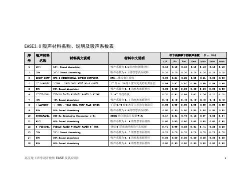
0.20
0。63
0。99
0。66
0.36
0。31
20
ACDECK 25
2"THK ACOUS DECK 16GA PERF STL DECK
2"声学覆盖物
0.54
0.97
1。00
0.91
0.55
0.31
0。31
21
ACOUSTILE
SUFACE TILE GLAZED/PERFORATED(AIR)
打有通气孔的光滑瓷砖
0.26
0.57
0。63
0.96
0.44
0.56
0。56
22
AC PLASTER
1/2” Thick Zonolite
0.5”泥灰
0.32
0。32
0.52
0。81
0.88
0。84
0。84
23
BAFL115F
1”X1。5# W/FABRIC COVER
1"X1.5#的墙面涂层
0。23
0.35
0。29
0。52
0。79
0。92
0。97
0。96
45
CIRRUS 75
CIRRUS 75 CEILING MATERIAL ARMSTONG
Armstong75浮云天花板材
0。36
0.38
0。67
0.89
0.97
1。00
1.00
46
CLAY BRICK
Bricks clay
粘土砖
0.16
0。13
0.08
0。24
0.57
0.69
0.71
金升阳 LHE20-20Bxx 电源模块产品说明书

20W ,AC-DC 模块电源产品特点●全球通用电压:85-264VAC/100-370VDC ●工作温度范围:-40℃to +85℃●4000VAC 高隔离电压●稳压输出、低纹波噪声●输出短路、过流、过压保护●高效率、高可靠性●全塑料外壳,符合UL94V-0●EMI性能满足CISPR32/EN55032CLASS B●通过IEC62368、UL62368、EN62368认证CB RoHSLHE20-20Bxx 系列-----是金升阳为客户提供的小体积模块式开关电源。
该系列电源具有全球输入电压范围、交直流两用、低功耗、高效率、高可靠性、安全隔离等优点。
产品安全可靠,EMC 性能好,EMC 及安全规格满足IEC62368、CISPR32/EN55032、UL62368和EN62368标准。
该系列产品广泛应用于工业、办公及民用等行业中,当应用于电磁兼容比较恶劣的环境时必须参考应用电路。
选型表认证产品型号输出功率标称输出电压及电流效率(230V AC,%/Typ.)最大容性负载(µF)UL/CE/CBLHE20-20B0311.55W 3.3V/3500mA 7336000LHE20-20B0515.5W5V/3100mA 7712240LHE20-20B0920W9V/2100mA 795600LHE20-20B1212V/1600mA 815000LHE20-20B1515V/1300mA 823000LHE20-20B2424V/850mA84900注:*产品型号后缀加“A2”为接线式封装拓展,后缀加“A4”为导轨式封装拓展,如:LHE20-20B03A2表示接线式封装,LHE20-20B03A4表示导轨式封装。
输入特性项目工作条件Min.Typ.Max.单位输入电压范围交流输入85--264VAC 直流输入100--370VDC 输入频率47--63Hz输入电流115V AC ----0.60A230V AC ----0.34冲击电流115V AC --20--230V AC--30--外接保险管推荐值2A/250V ,慢断,必接热插拔不支持输出特性项目工作条件Min.Typ.Max.单位输出电压精度 3.3V 输出--±3--%其他输出--±2--线性调节率满载--±0.5--负载调节率0%-100%负载--±1--纹波噪声*20MHz 带宽(峰-峰值)--50100mV 温度漂移系数--±0.02--%/℃短路保护打嗝式,可长期短路,自恢复过流保护≥110%Io自恢复过压保护3.3/5VDC输出≤7.5VDC(输出电压钳位或打嗝) 9VDC输出≤15VDC(输出电压钳位或打嗝) 12/15VDC输出≤20VDC(输出电压钳位或打嗝) 24VDC输出≤30VDC(输出电压钳位或打嗝)最小负载0----%掉电保持时间115V AC输入--15--ms 230V AC输入--80--注:*纹波和噪声的测试方法采用平行线测试法,具体操作方法参见《AC-DC模块电源应用指南》。
ICE3BS03LJG中文资料
F3 PWM controllerICE3BS03LJGOff-Line SMPS Current Mode Controller with integrated 500V Startup Cell ( Latched and frequency jitter Mode )Power Management & SupplyVersion 2.0, 6 Dec 2007元器件交易网Edition 2007-12-6Published byInfineon Technologies AG,81726 Munich, Germany,© 2007 Infineon Technologies AG.All Rights Reserved.Legal disclaimerThe information given in this document shall in no event be regarded as a guarantee of conditions orcharacteristics. With respect to any examples or hints given herein, any typical values stated herein and/or any information regarding the application of the device, Infineon Technologies hereby disclaims any and all warranties and liabilities of any kind, including without limitation, warranties of non-infringement of intellectual property rights of any third rmationFor further information on technology, delivery terms and conditions and prices, please contact your nearest Infineon Technologies Office ().WarningsDue to technical requirements, components may contain dangerous substances. For information on the types in question, please contact your nearest Infineon Technologies Office.Infineon Technologies Components may be used in life-support devices or systems only with the express written approval of Infineon Technologies, if a failure of such components can reasonably be expected to cause the failure of that life-support device or system or to affect the safety or effectiveness of that device or system. Life support devices or systems are intended to be implanted in the human body or to support and/or maintain and sustain and/or protect human life. If they fail, it is reasonable to assume that the health of the user or other persons may be endangered.For questions on technology, delivery and prices please contact the Infineon Technologies Offices in Germany or the Infineon Technologies Companies and Representatives worldwide: see our webpage at F3 PWM controller ICE3BS03LJG Revision History:2007-12-6DatasheetPrevious Version: 1.0PageSubjects (major changes since last revision)Type Marking Package F OSC ICE3BS03LJG3BS3LJPG-DSO-865kHzF3 PWM controllerICE3BS03LJGOff-Line SMPS Current Mode Controller with integrated 500V Startup Cell ( Latched and frequency jitter Mode )DescriptionThe ICE3BS03LJG is the latest version of the F3 controller for lowest standby power and low EMI features with both auto-restart and latch off protection features to enhance the system robustness. It targets for off-Line battery adapters, and low cost SMPS for low to medium power range such as application for the DVD R/W, DVD Combi,Blue Ray DVD player and recorder, set top box, charger,note book adapter, etc. The inherited outstanding features includes 500V startup cell, active burst mode (achieve the lowest standby power; i.e. <100mV at no load with Vin =270Vac) and propagation delay compensation (accurate output power limit for wide range input),modulated gate drive (low EMI), etc. The newly added technology and features can further enhance the features.It includes BiCMOS technology (further lower power consumption and extend Vcc operating range to 26V),frequency jittering feature (low EMI), built-in soft start,built-in blanking window with extendable blanking time for high load jump, external latch off enable pin (feasible for extra protection), etc. Therefore, ICE3BS03LJG is a versatile PWM controller for low to medium power application.Product Highlights•Active Burst Mode to reach the lowest Standby Power Requirements < 100mW•Built-in latched Off protection Mode and external latch enable function to increase robustness of the system•Built-in and extendable blanking Window for high load jumps to increase system reliability •Frequency jitter for low EMI•Pb-free lead plating; RoHS compilantFeatures•500V Startup Cell switched off after Start Up •Active Burst Mode for lowest Standby Power •Fast load jump response in Active Burst Mode •65kHz internally fixed switching frequency •Built-in Latched Off Protection Mode forOvertemperature, Overvoltage & Short Winding •Auto Restart Protection Mode for Overload, Open Loop & VCC Undervoltage •Built-in Soft Start•Built-in blanking window with extendable blanking time for short duration high current •External latch off enable function •Max Duty Cycle 75%•Overall tolerance of Current Limiting < ±5%•Internal PWM Leading Edge Blanking•BiCMOS technology provide wide VCC range •Frequency jitter and soft gate driving for low EMITable of Contents Page 1Pin Configuration and Functionality . . . . . . . . . . . . . . . . . . . . . . . . . . . . .5 1.1Pin Configuration with PG-DSO-8 . . . . . . . . . . . . . . . . . . . . . . . . . . . . . . . . .5 1.2Pin Functionality . . . . . . . . . . . . . . . . . . . . . . . . . . . . . . . . . . . . . . . . . . . . . .52Representative Blockdiagram . . . . . . . . . . . . . . . . . . . . . . . . . . . . . . . . . .63Functional Description . . . . . . . . . . . . . . . . . . . . . . . . . . . . . . . . . . . . . . . .7 3.1Introduction . . . . . . . . . . . . . . . . . . . . . . . . . . . . . . . . . . . . . . . . . . . . . . . . . .7 3.2Power Management . . . . . . . . . . . . . . . . . . . . . . . . . . . . . . . . . . . . . . . . . . . .7 3.3Improved Current Mode . . . . . . . . . . . . . . . . . . . . . . . . . . . . . . . . . . . . . . . . .8 3.3.1PWM-OP . . . . . . . . . . . . . . . . . . . . . . . . . . . . . . . . . . . . . . . . . . . . . . . . . .9 3.3.2PWM-Comparator . . . . . . . . . . . . . . . . . . . . . . . . . . . . . . . . . . . . . . . . . . .9 3.4Startup Phase . . . . . . . . . . . . . . . . . . . . . . . . . . . . . . . . . . . . . . . . . . . . . . .10 3.5PWM Section . . . . . . . . . . . . . . . . . . . . . . . . . . . . . . . . . . . . . . . . . . . . . . . .11 3.5.1Oscillator . . . . . . . . . . . . . . . . . . . . . . . . . . . . . . . . . . . . . . . . . . . . . . . . .11 3.5.2PWM-Latch FF . . . . . . . . . . . . . . . . . . . . . . . . . . . . . . . . . . . . . . . . . . . . .12 3.5.3Gate Driver . . . . . . . . . . . . . . . . . . . . . . . . . . . . . . . . . . . . . . . . . . . . . . .12 3.6Current Limiting . . . . . . . . . . . . . . . . . . . . . . . . . . . . . . . . . . . . . . . . . . . . . .12 3.6.1Leading Edge Blanking . . . . . . . . . . . . . . . . . . . . . . . . . . . . . . . . . . . . . .13 3.6.2Propagation Delay Compensation . . . . . . . . . . . . . . . . . . . . . . . . . . . . . .13 3.7Control Unit . . . . . . . . . . . . . . . . . . . . . . . . . . . . . . . . . . . . . . . . . . . . . . . . .14 3.7.1Basic and Extendable Blanking Mode . . . . . . . . . . . . . . . . . . . . . . . . . . .14 3.7.2Active Burst Mode . . . . . . . . . . . . . . . . . . . . . . . . . . . . . . . . . . . . . . . . . .14 3.7.2.1Entering Active Burst Mode . . . . . . . . . . . . . . . . . . . . . . . . . . . . . . . . .15 3.7.2.2Working in Active Burst Mode . . . . . . . . . . . . . . . . . . . . . . . . . . . . . . .15 3.7.2.3Leaving Active Burst Mode . . . . . . . . . . . . . . . . . . . . . . . . . . . . . . . . .15 3.7.3Protection Modes . . . . . . . . . . . . . . . . . . . . . . . . . . . . . . . . . . . . . . . . . . .16 3.7.3.1Latched Off Mode . . . . . . . . . . . . . . . . . . . . . . . . . . . . . . . . . . . . . . . .16 3.7.3.2Auto Restart Mode . . . . . . . . . . . . . . . . . . . . . . . . . . . . . . . . . . . . . . . .17 4Electrical Characteristics . . . . . . . . . . . . . . . . . . . . . . . . . . . . . . . . . . . . .18 4.1Absolute Maximum Ratings . . . . . . . . . . . . . . . . . . . . . . . . . . . . . . . . . . . . .18 4.2Operating Range . . . . . . . . . . . . . . . . . . . . . . . . . . . . . . . . . . . . . . . . . . . . .18 4.3Characteristics . . . . . . . . . . . . . . . . . . . . . . . . . . . . . . . . . . . . . . . . . . . . . . .19 4.3.1Supply Section . . . . . . . . . . . . . . . . . . . . . . . . . . . . . . . . . . . . . . . . . . . . .19 4.3.2Internal Voltage Reference . . . . . . . . . . . . . . . . . . . . . . . . . . . . . . . . . . .19 4.3.3PWM Section . . . . . . . . . . . . . . . . . . . . . . . . . . . . . . . . . . . . . . . . . . . . . .20 4.3.4Soft Start time . . . . . . . . . . . . . . . . . . . . . . . . . . . . . . . . . . . . . . . . . . . . .20 4.3.5Control Unit . . . . . . . . . . . . . . . . . . . . . . . . . . . . . . . . . . . . . . . . . . . . . . .21 4.3.6Current Limiting . . . . . . . . . . . . . . . . . . . . . . . . . . . . . . . . . . . . . . . . . . . .22 4.3.7Driver Section . . . . . . . . . . . . . . . . . . . . . . . . . . . . . . . . . . . . . . . . . . . . .22 5Outline Dimension . . . . . . . . . . . . . . . . . . . . . . . . . . . . . . . . . . . . . . . . . . .23 6Marking . . . . . . . . . . . . . . . . . . . . . . . . . . . . . . . . . . . . . . . . . . . . . . . . . . . .24Pin Configuration and Functionality1Pin Configuration and Functionality1.1Pin Configuration with PG-DSO-8 Figure1Pin Configuration PG-DSO-8(top view)1.2Pin FunctionalityBL (extended Blanking and Latch off enable)The BL pin combines the functions of extendable blanking time for entering the Auto Restart Protection Mode and the external latch off enable. The extendable blanking time function is to extend the built-in 20ms blanking time by adding an external capacitor at BL to ground. The external latch off enable function is an external access to latch off the IC. It is triggered by pulling down the BL pin to less than 0.25V.FB (Feedback)The information about the regulation is provided by the FB Pin to the internal Protection Unit and to the internal PWM-Comparator to control the duty cycle. The FB-Signal is the only control in case of light load at the Active Burst Mode.CS (Current Sense)The Current Sense pin senses the voltage developed on the series resistor inserted in the source of the Power MOSFET. If CS reaches the internal threshold of the Current Limit Comparator, the Driver output is immediately switched off. Furthermore, this current information can be used to realize the Current Mode operation through the PWM-Comparator where it compares with FB signal.GateThe Gate pin is the output of the internal driver stage connected to the Gate of an external power MOSFET.HV (High Voltage)The high voltage Pin is connected to the rectified DC input voltage. It is the input for the integrated 500V Startup cell.VCC (Power supply)The VCC pin is the positive supply of the IC. The operating range is between 10.5V and 26V.GND (Ground)The GND pin is the ground of the controller.Pin Symbol Function1BL extended Blanking and Latch offenable2FB Feedback3CS Current Sense4Gate Gate driver output5HV High Voltage input6n.c.Not Connected7VCC Controller Supply Voltage8GNDController GroundRepresentative Blockdiagram 2Representative BlockdiagramFigure2Representative Blockdiagram3Functional DescriptionAll values which are used in the functional description are typical values. For calculating the worst cases the min/max values which can be found in section 4 Electrical Characteristics have to be considered.3.1IntroductionICE3BS03LJG is an enhanced version of the F3 PWM controller (ICE3xS02) for the low to medium power application. The particular enhanced features are the built-in features for soft start, blanking window and frequency jitter. It also provides the flexibility to increase the blanking window by simply adding capacitor in BL pin. To increase the robustness and flexibility of the protection feature, an external latch-off enable feature is added. Moreover, the proven outstanding features in F3 PWM controller are still remained such as the active burst mode, propagation delay compensation, modulated gate drive, protection for Vcc overvoltage, over temperature, over load, open loop, etc.The intelligent Active Burst Mode at Standby Mode can effective obtain the lowest Standby Power at minimum load and no load conditions. After entering this burst mode, there is still a full control of the power conversion by the secondary side via the same optocoupler that is used for the normal PWM control. The response on load jumps is optimized. The voltage ripple on V out is minimized. V out is on well controlled in this mode.The usual externally connected RC-filter in the feedback line after the optocoupler is integrated in the IC to reduce the external part count.Furthermore, a high voltage Startup Cell is integrated into the IC which is switched off once the Undervoltage Lockout on-threshold of 18V is exceeded. The external startup resistor is no longer necessary as this Startup Cell can directly connected to the input bulk capacitor. Power losses are therefore reduced. This increases the efficiency under light load conditions drastically. Adopting the BiCMOS technology, it can further decrease the power consumption and provide a even better standby input power. Besides, it also increases the design flexibility as the Vcc voltage range is extended to 26V.The built-in soft start time at 20ms can provide sufficient timing to reduce the over-stress at power MOSFET and the output rectifier during startup. There are 2 modes of blanking time for high load jumps; the basic mode and the extendable mode. The blanking time for the basic mode is set at 20ms while the extendable mode will increase the blanking time at basic mode by adding external capacitor at the BL pin. During this time window the overload detection is disabled. With this concept no further external components are necessary to adjust the blanking window.In order to increase the robustness and safety of the system, the IC provides 2 levels of protection modes: Latched Off Mode and Auto Restart Mode. The Latched Off Mode is only entered under dangerous conditions which can damage the SMPS if not switched off immediately. A restart of the system can only be done by recycling the AC line. In addition, for this enhanced version, there is an external Latch Enable function provided to increase the flexibility in protection. When the BL pin is pulled down to less than 0.25V, the Latch Off Mode is triggered.The Auto Restart Mode reduces the average power conversion to a minimum under unsafe operating conditions. This is necessary for a prolonged fault condition which could otherwise lead to a destruction of the SMPS over time. Once the malfunction is removed, normal operation is automatically retained after the next Start Up Phase.The internal precise peak current control reduces the costs for the transformer and the secondary diode. The influence of the change in the input voltage on the maximum power limitation can be avoided together with the integrated Propagation Delay Compensation. Therefore the maximum power is nearly independent on the input voltage, which is required for wide range SMPS. Thus there is no need for the over-sizing of the SMPS, e.g. the transformer and the output diode. Furthermore, this enhanced version implements the frequency jitter mode to the switching clock and modulated gate drive signal at the Gate pin such that the EMI noise will be effectively reduced.3.2Power ManagementThe Undervoltage Lockout monitors the external supply voltage V VCC. When the SMPS is plugged to the main line, the internal Startup Cell is biased and starts to charge the external capacitor C VCC which is connected to the VCC pin. This VCC charge current is controlled to 0.9mA by the Startup Cell. When the V VCC exceeds the on-threshold V CCon=18V, the bias circuit are switched on. Then the Startup Cell is switched off by the Undervoltage Lockout and therefore no power losses present due to the connection of the Startup Cell to the Drain voltage. To avoid uncontrolled ringing at switch-on a hysteresis start up voltage is implemented. The switch-off of the controller can only take place after Active Mode was entered and V VCC falls below 10.5V. The maximum current consumption before the controller is activated is about 250µA.When V VCC falls below the off-threshold V CCoff=10.5V, the bias circuit switched off and the soft start counter isreset. Thus it is ensured that at every startup cycle the soft start starts at zero.Figure3Power ManagementThe internal bias circuit is switched off if Latched Off Mode or Auto Restart Mode is entered. The current consumption is then reduced to 250µA.Once the malfunction condition is removed, this block will then turn back on. The recovery from Auto Restart Mode does not require re-cycling the AC line. In case Latched Off Mode is entered, VCC needs to be dropped below 6.23V to reset the Latched Off Mode. This is done usually by re-cycling the AC line.When Active Burst Mode is entered, the internal Bias is switched off most of the time but the Voltage Reference is kept alive in order to reduce the current consumption below 450µA. 3.3Improved Current ModeFigure4Current ModeCurrent Mode means the duty cycle is controlled by the slope of the primary current. This is done by comparing the FB signal with the amplified current sense signal.Figure5Pulse Width ModulationIn case the amplified current sense signal exceeds the FB signal, the on-time T on of the driver is finished by resetting the PWM-Latch (see Figure 5).The primary current is sensed by the external series resistor R Sense inserted in the source of the external power MOSFET. By means of Current Mode regulation, the secondary output voltage is insensitiveto the line variations. The current waveform slope will change with the line variation, which controls the duty cycle.The external R Sense allows an individual adjustment of the maximum source current of the external power MOSFET.To improve the Current Mode during light load conditions the amplified current ramp of the PWM-OP is superimposed on a voltage ramp, which is built by the switch T2, the voltage source V1 and a resistor R1 (see Figure 6). Every time the oscillator shuts down for maximum duty cycle limitation the switch T2 is closed by V OSC. When the oscillator triggers the Gate Driver, T2 is opened so that the voltage ramp can start.In case of light load the amplified current ramp is too small to ensure a stable regulation. In that case the Voltage Ramp is a well defined signal for the comparison with the FB-signal. The duty cycle is then controlled by the slope of the Voltage Ramp.By means of the time delay circuit which is triggered by the inverted V OSC signal, the Gate Driver is switched-off until it reaches approximately 156ns delay time (see Figure 7). It allows the duty cycle to be reduced continuously till 0% by decreasing V FB below that threshold.Figure6Improved Current Mode Figure7Light Load Conditions3.3.1PWM-OPThe input of the PWM-OP is applied over the internal leading edge blanking to the external sense resistor R Sense connected to pin CS. R Sense converts the source current into a sense voltage. The sense voltage is amplified with a gain of 3.2 by PWM OP. The output of the PWM-OP is connected to the voltage source V1. The voltage ramp with the superimposed amplified current signal is fed into the positive inputs of the PWM-Comparator C8 and the Soft-Start-Comparator (see Figure 6).3.3.2PWM-ComparatorThe PWM-Comparator compares the sensed current signal of the external power MOSFET with the feedback signal V FB (see Figure 8). V FB is created by an external optocoupler or external transistor in combination with the internal pull-up resistor R FB and provides the load information of the feedback circuitry. When the amplified current signal of the external power MOSFET exceeds the signal V FB the PWM-Comparator switches off the Gate Driver.Figure8PWM Controlling3.4Startup PhaseFigure9Soft StartIn the Startup Phase, the IC provides a Soft Start period to control the maximum primary current by means of a duty cycle limitation. The Soft Start function is a built-in function and it is controlled by an internal counter.Figure10Soft Start PhaseWhen the V VCC exceeds the on-threshold voltage, the IC starts the Soft Start mode (see Figure 10).The function is realized by an internal Soft Start resistor, an current sink and a counter. And the amplitude of the current sink is controlled by the counter (see Figure 11).Figure11Soft Start CircuitAfter the IC is switched on, the V SFOFTS voltage is controlled such that the voltage is increased step-wisely (32 steps) with the increase of the counts. The Soft Start counter would send a signal to the current sink control in every 600us such that the current sinkdecrease gradually and the duty ratio of the gate drive increases gradually. The Soft Start will be finished in 20ms (T Soft-Start) after the IC is switched on. At the end of the Soft Start period, the current sink is switched off.Figure12Gate drive signal under Soft-Start Phase Within the soft start period, the duty cycle is increasing from zero to maximum gradually (see Figure 12).Figure13Start Up Phase In addition to Start-Up, Soft-Start is also activated at each restart attempt during Auto Restart.The Start-Up time T Start-Up before the converter output voltage V OUT is settled, must be shorter than the Soft-Start Phase T Soft-Start (see Figure 13).By means of Soft-Start there is an effective minimization of current and voltage stresses on the external power MOSFET, the clamp circuit and the output overshoot and it helps to prevent saturation of the transformer during Start-Up.3.5PWM SectionFigure14PWM Section Block3.5.1OscillatorThe oscillator generates a fixed frequency of 65KHz with frequency jittering of ±4% (which is ±2.6KHz) at a jittering period of 4ms.A capacitor, a current source and a current sink which determine the frequency are integrated. The charging and discharging current of the implemented oscillator capacitor are internally trimmed, in order to achieve a very accurate switching frequency. The ratio of controlled charge to discharge current is adjusted to reach a maximum duty cycle limitation of D max=0.75. Once the Soft Start period is over and when the IC goes into normal operating mode, the switching frequency of the clock is varied by the control signal from the SoftStart block. Then the switching frequency is varied in range of 65KHz ± 2.6KHz at period of 4ms.3.5.2PWM-Latch FFThe output of the oscillator block provides continuous pulse to the PWM-Latch which turns on/off the external power MOSFET. After the PWM-Latch is set, it is reset by the PWM comparator, the Soft Start comparator or the Current -Limit comparator. When it is in reset mode, the output of the gate driver is shut down immediately.3.5.3Gate DriverFigure15Gate DriverThe driver-stage is optimized to minimize EMI and to provide high circuit efficiency. This is done by reducing the switch on slope when exceeding the external power MOSFET threshold. This is achieved by a slope control of the rising edge at the gate driver’s output (see Figure 16).Figure16Gate Rising Slope Thus the leading switch on spike is minimized. Furthermore the driver circuit is designed to eliminate cross conduction of the output stage.During power up, when VCC is below the undervoltage lockout threshold V VCCoff, the output of the Gate Driver is set to low in order to disable power transfer to the secondary side.3.6Current LimitingFigure17Current Limiting BlockThere is a cycle by cycle peak current limiting operation realized by the Current-Limit comparator C10. The source current of the external power MOSFET is sensed via an external sense resistor R Sense. By means of R Sense the source current is transformed to a sense voltage V Sense which is fed into the pin CS. If the voltage V Sense exceeds the internal threshold voltage V csth, the comparator C10 immediately turns off the gate drive by resetting the PWM Latch FF1.A Propagation Delay Compensation is added to support the immediate shut down of the external power MOSFET with very short propagation delay. Thus the influence of the AC input voltage on the maximum output power can be reduced to minimal.In order to prevent the current limit from distortions caused by leading edge spikes, a Leading EdgeBlanking is integrated in the current sense path for the comparators C10, C12 and the PWM-OP.The output of comparator C12 is activated by the AND Gate G10 if Active Burst Mode is entered. When it is activated, the current limiting is reduced to 0.25V. This voltage level determines the maximum power level in Active Burst Mode.Furthermore, the comparator C11 is implemented to detect dangerous current levels which could occur if there is a short winding in the transformer or the secondary diode is shorten. To ensure that there is no accidentally entering of the Latched Mode by the comparator C11, a 190ns spike blanking time is integrated in the output path of comparator C11.3.6.1Leading Edge BlankingFigure18Leading Edge BlankingWhenever the power MOSFET is switched on, a leading edge spike is generated due to the primary-side capacitances and reverse recovery time of the secondary-side rectifier. This spike can cause the gate drive to switch off unintentionally. In order to avoid a premature termination of the switching pulse, this spike is blanked out with a time constant of t LEB = 220ns. 3.6.2Propagation Delay CompensationFigure19Current LimitingIn case of overcurrent detection, there is always propagation delay to switch off the external power MOSFET. An overshoot of the peak current I peak is induced to the delay, which depends on the ratio of dI/ dt of the peak current (see Figure 19).The overshoot of Signal2 is larger than of Signal1 due to the steeper rising waveform. This change in the slope is depending on the AC input voltage. Propagation Delay Compensation is integrated to reduce the overshoot due to dI/dt of the rising primary current. Thus the propagation delay time between exceeding the current sense threshold V csth and the switching off of the external power MOSFET is compensated over temperature within a wide range. Current Limiting is then very accurate.For example, I peak = 0.5A with R Sense = 2. The current sense threshold is set to a static voltage level V csth=1V without Propagation Delay Compensation. A current ramp of dI/dt = 0.4A/µs, or dV Sense/dt = 0.8V/µs, and a propagation delay time of t Propagation Delay =180ns leads to an I peak overshoot of 14.4%. With the propagation delay compensation, the overshoot is only around 2% (see Figure 20).Figure20Overcurrent ShutdownFigure21Dynamic Voltage Threshold V csthThe Propagation Delay Compensation is realized by means of a dynamic threshold voltage V csth (see Figure 21). In case of a steeper slope the switch off of the driver is earlier to compensate the delay.3.7Control UnitThe Control Unit contains the functions for Active Burst Mode, Auto Restart Mode and Latched Off Mode. The Active Burst Mode and the Auto Restart Mode both have 20ms internal Blanking Time. For the Auto Restart Mode, a further extendable Blanking Time is achieved by adding external capacitor at BL pin. By means of this Blanking Time, the IC avoids entering into these two modes accidentally. Furthermore those buffer time for the overload detection is very useful for the application that works in low current but requires a short duration of high current occasionally.3.7.1Basic and Extendable Blanking ModeFigure22Basic and Extendable Blanking Mode There are 2 kinds of Blanking mode; basic mode and the extendable mode. The basic mode has an internal pre-set 20ms blanking time while the extendable mode has extended blanking time to basic mode by connecting an external capacitor to the BL pin. For the extendable mode, the gate G5 is blocked even though the 20ms blanking time is reached if an external capacitor C BK is added to BL pin. While the 20ms blanking time is passed, the switch S1 is opened by G2. Then the 0.9V clamped voltage at BL pin is charged to 4.0V through the internal I BK constant current. Then G5 is enabled by comparator C3. After the 30us spike blanking time, the Auto Restart Mode is activated.For example, if C BK = 0.22uF, I BK = 13uABlanking time = 20ms + C BK x (4.0 - 0.9) / I BK = 72ms The 20ms blanking time circuit after C4 is disabled by the soft stat block such that the controller can start up properly.The Active Burst Mode has basic blanking mode only while the Auto Restart Mode has both the basic and the extendable blanking mode.3.7.2Active Burst ModeThe IC enters Active Burst Mode under low load conditions. With the Active Burst Mode, the efficiency increases significantly at light load conditions while still maintaining a low ripple on V OUT and a fast response on load jumps. During Active Burst Mode, the IC is controlled by the FB signal. Since the IC is always active, it can be a very fast response to the quick change at the FB signal. The Start up Cell is kept OFF in order to minimize the power loss.Figure23Active Burst ModeThe Active Burst Mode is located in the Control Unit. Figure 23 shows the related components.。
THS3202中文资料

−50 −60 HD − Hormonic Distortion − dB −70 −80 −90 −100 3rd Harmonic −110 −120 0 2 4 6 8 10 12 VO − Output Voltage − Vpp G=5 RL = 500 Ω VCC = 15 V Rf = 420 Ω f = 10 MHz 50 48 46 44 OIP 3 − dBc 42 40 38 36 34 32 30 28 26 10 60
16.5 V ±VS ±3 V 175 mA
See Dissipation Rating Table
Continuous power dissipation TJ (3)
150°C 125°C −40°C to 85°C −65°C to 150°C 300°C 3000 V 1500 V 200 V
Copyright 2002 − 2004, Texas Instruments Incorporated
元器件交易网
THS3202
SLOS242D − SEPTEMBER 2002 − REVISED JANUARY 2004
ABSOLUTE MAXIMUM RATINGS
OIP3 vs FREQUENCY
Test Instrument Measurement Limit VCC = ±7.5 V VCC = ±7 V VCC = ±6 V
TEST CIRCUIT FOR IMD3 / OIP3
Output Power Spectrum Analyzer
2nd Harmonic
Maximum junction temperature, continuous operation, long term reliability TJ (4) Operating free-air temperature range, TA Storage temperature range, Tstg Lead temperature 1,6 mm (1/16 inch) from case for 10 seconds
2380中文资料
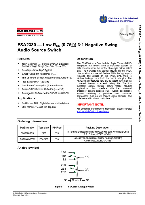
February 2007© 2006 Fairchild Semiconductor CorporationFSA2380 Rev. 1.0.2FSA2380 — Low R ON (0.75Ω) 3:1 Negative Swing Audio Source SwitchClick here for this datasheet translated into Chinese!FSA2380 — Low R ON (0.75Ω) 3:1 Negative Swing Audio Source SwitchFeatures 10µA Maximum I CCT Current Over An Expanded Control Voltage Range (V IN =2.6V, V CC =4.3V) C ON Capacitance 70pF Typical 0.75Ω Typical On Resistance (R ON )1Bn, 2Bn Ports Support Negative Swing Audio to -2V -3db Bandwidth: > 120 MHzLow Power Consumption (1µA maximum) Power-Off Feature for 1A/2A Pin (I IN < 2µA) Packaged in Pb-Free 14-Pin TSSOP and DQFNApplicationsCell Phone, PDA, Digital Camera, and NotebookLCD Monitor, TV, and Set-Top BoxDescriptionThe FSA2380 is a Double-Pole, Triple Throw (DP3T) multiplexer that routes three dual-channel sources of data or audio under the control of a single pair of select pins. The FSA2380 has special circuitry on the 1A/2A pins to allow a power-off feature. With the V CC supply removed and voltage on the 1A/2A pins, there is minimal leakage current into the 1A/2A data pins. The FSA2380 also features very low quiescent current and a power-off feature to extend battery life. The low quiescent current feature allows mobile handset applications direct interface with the baseband processor general-purpose I/Os. Typical applications involve switching in portables and consumer applications, such as cell phones, digital cameras, and notebooks with hubs or controllers.IMPORTANT NOTE:For additional performance information, please contact analogswitch@ .Ordering InformationPart NumberTop MarkPb-FreePacking DescriptionFSA2380BQX 2380 Yes 14-Terminal Depopulated very thin Quad Flat-pack No leads (DQFN)2.5 x3.0mm, JEDEC MO-241FSA2380MTCX FSA2380 Yes14-Lead Thin Shrink Small Outline Package (TSSOP)4.4mm wide, JEDEC MO-153Analog SymbolControl S0S12B02B22A2B11B01B21A1B1Figure 1.FSA2380 Analog Symbol™TinyBoost© 2006 Fairchild Semiconductor Corporation FSA2380 Rev. 1.0.2 13。
华尔康净水设备导购员培训手册

华尔康净水设备导购员培训手册华尔康净水设备目录第一章:华尔康简介...........................................................................................................1.华尔康辉煌旅程......................................................................................................2.华尔康净水简介...................................................................................................... 第二章:健康水知识...........................................................................................................1、水与人体的关系......................................................................................................2、水对人体的作用......................................................................................................3、健康水标准.............................................................................................................. 第三章:产品知识...............................................................................................................1.产品的命名规则......................................................................................................2.水处理设备的名称命名..........................................................................................3.净水设备工艺原理阐述..........................................................................................3.1活性炭系列净水工艺原理............................................................................3.2陶瓷系列净水工艺原理:............................................................................3.3反渗透系列净水工艺原理............................................................................4.各款产品及滤芯卖点.................................................................................................4.1◆MRO105-5 原型号:MYJ5RO396CC ........................................................4.2◆MU104-5 原型号:MT-3(395CC) .......................................................4.3◆MRO101-5 原型号:MYJ5RO382C ...........................................................4.4◆MC101-3 原型号:MC-3(380CC)-3 ....................................................4.5◆MC101-4 原型号:MC-3(380CC)-4 ....................................................4.6◆MT101-5 原型号:MT-3(380CC)-5 .....................................................4.7◆MU106-L .......................................................................................................4.8◆MRO107-L .....................................................................................................4.9◆MS110-1.5T ...................................................................................................5.0◆MU109-0.6T ..................................................................................................5.滤芯功能性介绍:.....................................................................................................6、重要零部件介绍:.................................................................................................. 第四章:导购员营销技巧...................................................................................................1.◆导购员的职业定位.................................................................................................2.◆顾客服务技巧.........................................................................................................3.◆销售服务技巧......................................................................................................... 第五章:售后服务...............................................................................................................1、售后服务政策..........................................................................................................2、安全注意事项..........................................................................................................3、滤芯的更换周期......................................................................................................第一章:公司简介1.公司辉煌旅程2012年十六年新品陆续上市,同时申请22项专利,累计专利已达到30余件。
江苏思源互感器有限公司——思源电气

思源电 气75%
香港赫 兹25%
江苏思源赫兹互感器有限公司 成立于2004年8月,是由思源 电气股份有限公司与香港赫兹 有限公司双方合作,投资一亿 元人民币兴建的专业研发、生 产高压电流、电压互感器的高
1
新技2 术企业。 3
Sieyuan Electric
Copyright © Sieyuan Electric Co., Ltd. All Rights Reserved.
15
电压互感器种类
35~110kV油浸电磁式电压互感器
Sieyuan Electric
Copyright © Sieyuan Electric Co., Ltd. All Rights Reserved.
16
电压互感器种类
35~220kV SF6气体绝缘电压互感 器
Sieyuan Electric
铁心 屏蔽 罩壳二次引线通过中间铝管引到产品
底部的出线盒里,铝管能够承
载短路电流,一旦头部发生故
障时,能将短路电流接地,避
二次引 线管
免套管部分发生爆炸。
Sieyuan Electric
Copyright © Sieyuan Electric Co., Ltd. All Rights Reserved.
31
C、产品的竞争优势
1 绝缘性能优异:电容屏套管采用整张进口高强度电缆纸绕制,工艺分散性小。80 %工频耐压值下局放小于5pC(国内外还没有厂家提出在80%工频耐压值下测局 放)。整体真空干燥注油工艺,避免二次受潮。介损稳定不回升。
2 全密封结构:全密封结构,德国进口 焊接机器人焊接代替传统的手工焊接, 提高焊接工艺,保证产品不漏油,免 维护。
Sieyuan Electric
LG NB3520A 300W条形音响系统 使用说明书
的位置。
电击的危险。
此设备配备便携式电池或蓄电池。
三角形内的惊叹号提醒用户, 随设备一起提供的印刷品中包 含重要的操作和维护(维修) 指南。
警告: 为了减少火灾或电击的危险,请勿使此 产品淋雨或暴露在潮湿的空气中。
小心: 切勿把电器暴露于有水(滴水或溅水)的 地方,而且不应将载有液体的对象(如花瓶) 放置于本电器上。
ཉེན་འགོག་སྲུང་སྐྱོང་སྐྱི་མོ་འདི་ལེན་མི་རུང་། གལ་ཏེ་སྐྱི་མོ་འདི་བླངས་ན་གནོད་ཚབས་ཆེ་ བའི་ཉེན་ཁ་ཆེ་རུ་འགྲོ་སྲིད།
ئاگاھلاندۇرۇش بۇ ئۈسكۈنىنىڭ كاتود نۇرى لامپىسىغا ئاسراش
1
小心
电击危险 请勿打开
规格页并加以确认。请不要让电源插座过载。 插座过载、插座松动或损坏、电线加长、电线 磨损、电线损坏或出现裂纹都会产生危险。出
现任意一种情况都会导致电击或火灾。请定期
小心: 为了减少电击的危险,请勿拆下前盖( 检查电器电源线,如果有损坏的迹象,拔下插
或后盖) 内部没有任何用户可以维修的零部件 头,停止使用此电器,然后由经授权的服务中
དྲན་སྐུལ་ཐ་ཚིག གནོད་འཚེ་མི་ཡོང་བའི་ཕྱིར་ངེས་པར་དུ་སྒྲིག་སྦྱར་གསལ་བཤད་ཡི་གེའི་ནང་གསལ་ གཏན་འབེབས་ལྟར་སྒྲིག་ཆས་པང་གཅལ/ རྩིག་ངོས་སུ་སྒྲིག་སྦྱོར་བརྟན་པོ་བྱ་དགོས་།
སྒྲིག་ཆས་འདིའི་སྐུད་ཡོད་འཕྲིན་དྲའི་གནམ་སྐུད་དང་འབྲེལ་མཐུད་བྱེད་སྐབས་ངེས་པར་དུ་ ཉེན་འགོག་ས་སྐུད་དང་
SAMPO 多媒体电浆显示器 说明书

歡迎使用SAMPO多媒體顯示器為能正確的操作使用,請仔細閱讀這本使用說明書●請妥善保管使用說明書及保證書,萬一使用中產生疑問或發生問題時,它也許能給您提供一些幫助。
●生產機號在品質管理上是很重要的,請確認顯示器上的生產機號與保證書上的生產機號是否一致。
Array免責聲明1.聲寶股份有限公司及著作人不對於此手冊的相關內容、適銷性或適合於某特定目的保證或擔保。
2.本公司保有修訂本出版品的權利,內容如有變更,恕不另行通知安全說明請詳讀及妥善保存此說明手冊,並依照產品本身所示之說明操作本產品。
使用本產品前,請注意下列指示:●安裝1.請將顯示器放置在平穩的桌上,若採壁掛方式請確定牆壁與結合體皆安全穩固。
2.將顯示器壁掛嵌入於室內裝潢時,應與牆壁保留10公分以上的散熱空間。
3.請勿將顯示器安裝於密閉或通風不良的廚架中。
4.請勿將本產品置於高溫,潮濕或多灰塵以及陽光可直接照射的地方;例如室外廣場、浴室、廚房、游泳池等場所。
5.本產品為家用產品,不適合安裝於車內、飛機及船艙使用。
6.建議您不要在喇叭或大型金屬旁操作本產品,以免受磁性干擾,影響本產品的畫質及色彩。
●清潔1.清潔機器時請將電源線拔掉,面板請使用乾淨軟布擦拭,勿用噴霧式清潔劑或有機溶劑擦擦拭,以免破壞面板表面2.請勿讓任何液體滲入機體內部,以免機器發生故障。
3.外殼擦拭必須使用軟布拭,不可使用揮發油,香蕉水等化學液體擦拭,以免塑膠外殼變質或塗料脫落。
●使用1.長時間不使用本產品時,請將電源線拔掉。
2.電源啟用時,請勿將插頭拔下。
3.搬運或移動本產品時務必拔下電源插頭,並需二人以上協力以確保安全。
4.顯示器從溫度較低的環境突然搬入較溫暖的環境時會產生結露,此時不可立即開機使用,請將電源關閉並放置一段時間後再行使用。
5.請勿長時間顯示靜止畫面,因為這會導致影像殘留。
●維修服務發生以下情形時請立即拔掉電源,並通知服務人員檢修。
┌電源線或電源插頭損壞。
├物品掉落機器內或有液體傾倒入機器內;機器置於水中或雨中。
飞利浦 逐点晶晰液晶电视 说明书
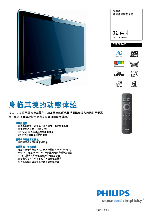
发行日期 2008-09-26 版本 : 1.0.3
12 NC: 8670 000 34725 EAN: 87 12581 37152 4
© 2008 Koninklijke Philips Electronics N.V. 保留所有权利。
规格如有更改,恕不另行通知。 所有商标是 Koninklijke Philips Electronics N.V. 或它们各自所有者 的财产。
即用 , 节目名称 , 排序 • 易于使用 : 自动音量调衡 , 侧控 • 屏幕显示语言 : 英语 , 简体中文
• 遥控器 : 电视 • 遥控器类型 : PF02A08B • 屏幕格式调整 : 4:3, 电脑扩展 14:9, 电脑扩展
16:9, 字幕缩放 , 超级变焦 , 宽银幕 • 智能模式: 游戏, 电影, 个人, 节能模式, 标准, 鲜
信息 (菜单语言) , 系统待机 • 前接/ 侧接: HDMI v1.3, S-video 输入, CVBS 输入
, 音频 L/R 输入 , 耳机输出 • 其它接口 : 模拟音频 L/R 输出 , 电脑音频输入 ,
VGA 电脑接口 , S/PDIF 输出 (同轴)
电源
• 环境温度 : 5 °C 至 35 °C • 主电源 : 100-240V、 50/60Hz • 功耗 : 150 瓦 • 待机功耗 : (标准) <0.3W
PC 输入 (VGA) 借助 PC 输入功能,您可以用一条 VGA 电缆将电 视机连接到电脑,将电视机用作电脑的显示器。
智能模式
优秀画面和音效取决于多种因素,如视频信号、 内容类型、居室环境、显示设备的类型,等等。 灵智模式预定义了画面和声音设置,根据您使用 电视的方式进行了方便的预设。 “ 个性化 ” 设置 允许您根据自己的喜好来定义图像设置,并存储 该设置以便将来能够轻松访问进行选择。所有这 些都方便地内置到了电视机中,从而实现了最佳 设置。
QZ22010-3L使用说明书
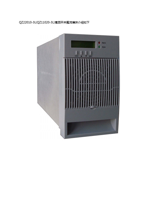
QZ22010-3L(QZ11020-3L)高频开关整流模块介绍如下目录一、概述 (2)二、电源模块功能特点 (2)三、电源模块技术指标 (4)四、电源模块外特性 (5)五、电源模块功能说明 (6)A.保护功能 (6)B.测量功能 (8)C.故障报警功能 (8)D.设置功能 (8)E.校准功能 (9)F.电池管理功能 (9)六、显示说明 (9)A.键盘及显示说明 (9)B.参数设置页: (10)C.开关机状态页: (11)D.测控校准页: (12)E.均浮充状态页: (12)F.故障信息显示页: (12)概述QZ22010-3L(QZ11020-3L)电源模块:功率级采用世界先进技术---------变频自然谐振软开关技术;控制上采用智能控制技术;功率器件一律使用进口器件;产品具有性能稳定、可靠性高、输出指标好等特点。
一、电源模块功能特点●LCD汉字显示,电源工作状态和工作参数一目了然,在系统主监控工作时,模块接收主监控发出的工作参数,无主监控器时,可以在模块面板上方便的设置模块工作参数,模块可脱离主监控器工作。
●软件校准技术该电源模块采用软件校准技术,模块内部没有一个电位器,通过按键和LCD显示可以校准输出电压、输出限流、电压测量、电流测量;参数调整方便快捷。
●自主均流技术模块采用自主均流技术,可多台模块并机工作,模块间均流偏差小于3%;●变频自然谐振软开关技术为了使开关电源能够在高频下高效率地运行,我公司不断研究开发高频软开关技术,已开发成功LC变频自然谐振技术,使开关过程损耗大为降低,从而进一步减小体积、减轻重量、极大提高电源模块的性能。
A、变频自然谐振软开关优点✧开关损耗小✧可实现高频化(极限頻率可做到1-2MHz)、开关过程在平滑状态下实现✧变频运行,谐波成份小✧无吸收电路电流、电压应力小B、LC 变频自然谐振软开关基本原理硬开关过程如图2-1,ZVS 软开关开关过程如图2-2,LC 变频自然谐振软开关开关过程如图2-3。
飞利利浦32PFL3409 32 英寸 HD Ready 液晶电视说明书

Philips 液晶电视32 英寸HD Ready32PFL3409明智的选择具有应用的便捷性和技术的前瞻性。
感受这款 1366 x 768 高清显示屏的出众画质和音质。
该电视采用高质量标准,可带给您绝佳的感官体验,您可以确信,这款飞利浦平板电视是您的明智之选。
便捷连接,轻松享受•兼容全高清视频输入的 2 路 HDMI (具有 Easylink )•个人电脑输入,使您可将电视机用作显示器•灵智图像和灵智声音,方便您个人观赏鲜艳、逼真的清晰图像•数码晶彩技术可带来出众的细节、层次和清晰度•高清液晶显示屏,1366 x 768•智能丽像可优化来自任何信号源的图像质量•影院模式带给您真实的影院体验清晰自然的音效•可增强音响享受的超宽环绕声•2 x 8 W 的清晰音质•动态低音增强带来影院级音效产品亮点数码晶彩技术数码晶彩技术是一种画面创新技术,这种技术采用数码方式通过优化对比度、色彩和清晰度,从而调节和优化画面质量。
看起来就像逼真的影院级图像。
液晶显示屏,1366 x 768这款 WXGA 显示屏采用了先进的 LCD 屏幕技术,具有 1366 x 768 的宽屏高清分辨率。
它可生成清晰流畅且无闪烁的逐行扫描图像以及优质的亮度和超凡的色彩。
此绚丽的图像将带给您增强的观看体验。
超宽环绕立体声超宽环绕声是飞利浦的音响技术,可显著放大声场,使您沉浸在音响世界。
超宽环绕声采用先进的电子相移技术,混合来自左右两侧的声音,从而扩展两个扬声器之间的虚拟距离。
这种更宽的传播空间大大增强了立体声效果,并产生更自然的声音维度。
超宽环绕声使您无需使用附加扬声器即可体验更深沉、更宽广的全方位环绕声。
2 x 8W 音响功率2 x 8 W 的清晰音质具有 Easylink 的 2 路 HDMI 输入EasyLink 利用 HDMI CEC 行业标准协议,在连接设备和电视之间共享功能。
有了 Easylink ,您只需一个遥控器即可操控电视和连接设备的主要功能。
- 1、下载文档前请自行甄别文档内容的完整性,平台不提供额外的编辑、内容补充、找答案等附加服务。
- 2、"仅部分预览"的文档,不可在线预览部分如存在完整性等问题,可反馈申请退款(可完整预览的文档不适用该条件!)。
- 3、如文档侵犯您的权益,请联系客服反馈,我们会尽快为您处理(人工客服工作时间:9:00-18:30)。
HZS-L SeriesSilicon Epitaxial Planar Zener Diode for Low Noise ApplicationADE-208-121A(Z)Rev 1Dec. 1996 Features• Diode noise level of this series is approximately 1/3-1/10 lower than the HZ series.• Low leakage, low zener impedance and maximum power dissipation of 400 mW are ideally suited for stabilized power supply, etc.• Wide spectrum from 5.2V through 38V of zener voltage provide flexible application.• Suitable for 5mm-pitch high speed automatic insertion.Ordering InformationType No.Mark Package CodeHZS-L Series Type No.MHDOutlineHZS-L Series2Absolute Maximum Ratings (Ta = 25°C)ItemSymbol Value Unit Power dissipation Pd 400mW Junction temperature Tj 200°C Storage temperatureTstg–55 to +175°CElectrical Characteristics (Ta = 25°C)Zener Voltage Reverese CurrentDynamic ResistanceV Z (V)*1TestCondition I R (µA)TestCondition r d (Ω)TestCondition Type Grade Min Max I Z (mA)Max V R (V)Max I Z (mA)HZS6LA1 5.2 5.50.512.01500.5A2 5.3 5.6A3 5.4 5.7B1 5.5 5.8800.5B2 5.6 5.9B3 5.7 6.0C1 5.8 6.1600.5C2 6.0 6.3C36.1 6.4HZS7LA1 6.3 6.60.51 3.5600.5A2 6.4 6.7A3 6.6 6.9B1 6.77.0B2 6.97.2B37.07.3C17.27.6C27.37.7C37.57.9HZS9LA17.78.10.51 6.0 600.5A27.98.3A38.18.5Note:1.Tested with DC.HZS-L Series3Zener Voltage Reverese CurrentDynamic ResistanceV Z (V)*1TestCondition I R (µA)TestCondition r d (Ω)TestCondition Type Grade Min Max I Z (mA)Max V R (V)Max I Z (mA)HZS9LB18.38.70.516.0600.5B28.58.9B38.79.1C18.99.3C29.19.5C39.39.7HZS11LA19.59.90.518.0 800.5A29.710.1A39.910.3B110.210.6B210.410.8B310.711.1C110.911.3C211.111.6C311.411.9HZS12LA111.612.10.5110.5 800.5A211.912.4A312.212.7B112.412.9B212.613.1B312.913.4C113.213.7C213.514.0C313.814.3HZS15L114.114.70.5113.0 800.5214.515.1314.915.5HZS16L115.315.90.5114.0 800.5215.716.5316.317.1Note:1.Tested with DC.HZS-L Series4Zener Voltage Reverese Current Dynamic ResistanceVZ(V)*1TestCondition IR(µA)TestCondition rd(Ω)TestConditionType Grade Min Max IZ (mA)Max VR(V)Max IZ(mA)HZS18L116.917.70.5115.0 800.5 217.518.3318.119.0HZS20L118.819.70.5118.01000.5 219.520.4320.221.1HZS22L120.921.90.5120.01000.5 221.622.6322.323.3HZS24L122.924.00.5122.01200.5 223.624.7324.325.5HZS27L125.226.60.5124.01500.5 226.227.6327.228.6HZS30L128.229.60.5127.02000.5 229.230.6330.231.6HZS33L131.232.60.5130.02500.5 232.233.6333.234.6HZS36L134.235.70.5133.03000.5 235.336.8336.438.0Note: 1.Tested with DC.Note: 2.Type No. is as follows; HZS6A1L, HZS6A2L, HZS36-3LHZS-L Series Main Characteristic5HZS-L SeriesPackage DimensionsUnit : mm6Cautions1.Hitachi neither warrants nor grants licenses of any rights of Hitachi’s or any third party’s patent,copyright, trademark, or other intellectual property rights for information contained in this document.Hitachi bears no responsibility for problems that may arise with third party’s rights, includingintellectual property rights, in connection with use of the information contained in this document.2.Products and product specifications may be subject to change without notice. Confirm that you have received the latest product standards or specifications before final design, purchase or use.3.Hitachi makes every attempt to ensure that its products are of high quality and reliability. However,contact Hitachi’s sales office before using the product in an application that demands especially high quality and reliability or where its failure or malfunction may directly threaten human life or cause risk of bodily injury, such as aerospace, aeronautics, nuclear power, combustion control, transportation,traffic, safety equipment or medical equipment for life support.4.Design your application so that the product is used within the ranges guaranteed by Hitachi particularly for maximum rating, operating supply voltage range, heat radiation characteristics, installationconditions and other characteristics. Hitachi bears no responsibility for failure or damage when used beyond the guaranteed ranges. Even within the guaranteed ranges, consider normally foreseeable failure rates or failure modes in semiconductor devices and employ systemic measures such as fail-safes, so that the equipment incorporating Hitachi product does not cause bodily injury, fire or other consequential damage due to operation of the Hitachi product.5.This product is not designed to be radiation resistant.6.No one is permitted to reproduce or duplicate, in any form, the whole or part of this document without written approval from Hitachi.7.Contact Hitachi’s sales office for any questions regarding this document or Hitachi semiconductor products.Hitachi, Ltd.Semiconductor & Integrated Circuits.Nippon Bldg., 2-6-2, Ohte-machi, Chiyoda-ku, Tokyo 100-0004, Japan Tel: Tokyo (03) 3270-2111 Fax: (03) 3270-5109Copyright ' Hitachi, Ltd., 1999. All rights reserved. Printed in Japan.Hitachi Asia Pte. Ltd.16 Collyer Quay #20-00Hitachi TowerSingapore 049318Tel: 535-2100Fax: 535-1533URLNorthAmerica : http:/Europe : /hel/ecg Asia (Singapore): .sg/grp3/sicd/index.htm Asia (Taiwan): /E/Product/SICD_Frame.htm Asia (HongKong): /eng/bo/grp3/index.htm Japan : http://www.hitachi.co.jp/Sicd/indx.htmHitachi Asia Ltd.Taipei Branch Office3F, Hung Kuo Building. No.167, Tun-Hwa North Road, Taipei (105)Tel: <886> (2) 2718-3666Fax: <886> (2) 2718-8180Hitachi Asia (Hong Kong) Ltd.Group III (Electronic Components)7/F., North Tower, World Finance Centre,Harbour City, Canton Road, Tsim Sha Tsui,Kowloon, Hong Kong Tel: <852> (2) 735 9218Fax: <852> (2) 730 0281 Telex: 40815 HITEC HXHitachi Europe Ltd.Electronic Components Group.Whitebrook ParkLower Cookham Road MaidenheadBerkshire SL6 8YA, United Kingdom Tel: <44> (1628) 585000Fax: <44> (1628) 778322Hitachi Europe GmbHElectronic components Group Dornacher Stra§e 3D-85622 Feldkirchen, Munich GermanyTel: <49> (89) 9 9180-0Fax: <49> (89) 9 29 30 00Hitachi Semiconductor (America) Inc.179 East Tasman Drive,San Jose,CA 95134 Tel: <1> (408) 433-1990Fax: <1>(408) 433-0223For further information write to:。
