PS2562L2-1-E4中文资料
PA2561L1-1(NEC)光耦规格书
DATA SHEETThe information in this document is subject to change without notice.©1992Document No. P12989EJ4V0DS00 (4th edition)(Previous No. LC-2225)Date Published August 1997 NS Printed in JapanPHOTOCOUPLERPS2561-1,-2, PS2561L-1,-2HIGH ISOLATION VOLTAGE SINGLE TRANSISTOR TYPE MULTI PHOTOCOUPLER SERIESThe mark shows major revised points.DESCRIPTIONThe PS2561-1, -2 and PS2561L-1, -2 are optically coupled isolators containing a GaAs light emitting diode and an NPN silicon phototransistor.PS2561-1, -2 are in a plastic DIP (Dual In-line Package) and PS2561L-1, -2 are lead bending type (Gull-wing) for surface mount.FEATURES•High isolation voltageBV = 5 000 Vr.m.s.: standard productsBV = 3 750 Vr.m.s.: VDE0884 approved products (Option)•High collector to emitter voltage (V CEO = 80 V)•High current transfer ratio (CTR = 200 % TYP.)•High-speed switching (t r = 3 µs TYP., t f = 5 µs TYP.)•UL approved (File No. E72422 (S) )•CSA approved (No. CA 101391)•BSI approved (BS415, BS7002) No. 7112•SEMKO approved (SS4410165) No. 9317144•NEMKO approved (NEK-HD 195S6) No. A21409•DEMKO approved (Section 101, 137) No. 300535•FIMKO approved (E69-89) No. 167265-08•VDE0884 approved (Option)APPLICATIONS•Power supply •Telephone/FAX.•FA/OA equipment•Programmable logic controller2PACKAGE DIMENSIONS (in millimeters)DIP Type5.1 MAX.6.53.8M A X .4.55M A X .2.8M I N .0.652.547.620.50 ± 0.100.25M4312PS2561-1 (New Package)10.2 MAX.1.25±0.156.53.8M A X .4.55M A X .2.8M I N .0.652.547.620.50 ± 0.100.25M871265340 to 15˚PS2561-20 to 15˚PS2561-14.6 ± 0.351.25±0.156.53.8M A X .4.55M A X .2.8M I N .0.650.50 ± 0.100.25M0 to 15˚7.622.5443121.25±0.15PS2561L1-15.1 MAX.6.53.8M A X .4.25M A X .2.8M I N .0.352.547.620.50 ± 0.100.25M0 to 15˚43121.25±0.1510.161. Anode 2. Cathode 3. Emitter 4. Collector 1, 3. Anode 2, 4. Cathode 5, 7. Emitter 6, 8. Collector1. Anode2. Cathode3. Emitter4. Collector 1. Anode 2. Cathode 3. Emitter 4. Collector Caution New package 1ch only3Lead Bending Type5.1 MAX.6.53.8M A X .2.547.620.25M4312PS2561L-1 (New Package)10.2 MAX.1.25±0.156.53.8M A X .2.547.6287126534PS2561L-2PS2561L-14.6 ± 0.351.25±0.156.53.8M A X .0.25M7.622.5443121.25±0.150.05 t o 0.29.60 ± 0.40.90 ± 0.250.05 t o 0.29.60 ± 0.40.90 ± 0.250.25M0.05 t o 0.29.60 ± 0.40.90 ± 0.255.1 MAX.6.53.8M A X .2.547.620.25MPS2561L2-143121.25±0.150.05 t o 0.210.160.9 ± 0.2512.0 MAX.1. Anode2. Cathode3. Emitter4. Collector1, 3. Anode 2, 4. Cathode 5, 7. Emitter 6, 8. Collector 1. Anode 2. Cathode 3. Emitter 4. Collector 1. Anode 2. Cathode 3. Emitter 4. Collector Caution New package 1ch only4ORDERING INFORMATIONPart NumberPackageSafety Standard ApprovalApplication partnumber *1PS2561-1PS2561L-1PS2561L1-1PS2561L2-14-pin DIP4-pin DIP (lead bending surface mount)4-pin DIP (for long distance)4-pin DIP (for long distance surfacemount)Standard products PS2561-1PS2561-2PS2561L-28-pin DIP8-pin DIP (lead bending surface mount)PS2561-2PS2561-1-V PS2561L-1-V PS2561L1-1-V PS2561L2-1-V 4-pin DIP4-pin DIP (lead bending surface mount)4-pin DIP (for long distance)4-pin DIP (for long distance surfacemount)VDE0884 approved products (Option)PS2561-1PS2561-2-V PS2561L-2-V8-pin DIP8-pin DIP (lead bending surface mount)PS2561-2*1 As applying to Safety Standard, following part number should be used.ABSOLUTE MAXIMUM RATINGS (T A = 25 °C, unless otherwise specified)ParameterSymbolRatingsUnitPS2561-1,PS2561L-1PS2561-2,PS2561L-2DiodeReverse Voltage V R 6V Forward Current (DC)I F80mAPower Dissipation Derating ∆P D /°C 1.5 1.2mW/°C Power Dissipation P D 150120mW/ch Peak Forward Current*1I FP 1A TransistorCollector to Emitter Voltage V CEO 80V Emitter to Collector Voltage V ECO 7V Collector CurrentI C50mA/chPower Dissipation Derating ∆P C /°C 1.5 1.2mW/°C Power DissipationP C 150120mW/ch Isolation Voltage*2BV5 0003 750*3Vr.m.s.Operating Ambient Temperature T A –55 to +100°C Storage TemperatureT stg–55 to +150°C*1PW = 100 µs, Duty Cycle = 1 %*2AC voltage for 1 minute at T A = 25 °C, RH = 60 % between input and output *3VDE0884 approved products (Option)•UL approved •CSA approved •BSI approved•NEMKO approved •DEMKO approved •SEMKO approved•FIMKO approved5ELECTRICAL CHARACTERISTICS (T A = 25 °C)ParameterSymbol Conditions MIN.TYP.MAX.Unit DiodeForward Voltage V F I F = 10 mA 1.171.4VReverse Current I R V R = 5 V5µA Terminal CapacitanceC t V = 0 V, f = 1.0 MHz 50pFTransistorCollector to Emitter Dark CurrentI CEOV CE = 80 V, I F = 0 mA100nACoupled Current Transfer Ratio *1CTR I F = 5 mA, V CE = 5 V 80200400%Collector Saturation VoltageV CE (sat)I F = 10 mA, I C = 2 mA0.3V Isolation Resistance R I-O V I-O = 1.0 kV 1011ΩIsolation Capacitance C I-O V = 0 V, f = 1.0 MHz0.5pFRise Time *2t r V CC = 10 V, I C = 2 mA, R L = 100 Ω3µsFall Time*2t f5*1CTR rank (only PS2561-1, PS2561L-1)*2Test circuit for switching timeL: 200 to 400 (%)M : 80 to 240 (%)D : 100 to 300 (%)H : 80 to 160 (%)W : 130 to 260 (%)V CCV OUTR L = 100 Ω50 ΩI F µPulse InputPW = 100 sDuty Cycle = 1/106TYPICAL CHARACTERISTICS (T A = 25 °C, unless otherwise specified)150100500255075100125150 1.5 mW/˚C1.2 mW/˚C15010050255075100125150010 0001001 000100101755025–25–50V CE = 80 V10 1.00.80.60.40.20510.50.110 m A401.5 mW/˚C1.2 mW/˚C20 m A 50 m A 2 m AI F = 1 mA5 m A 70260504030201004681020 m A I F = 5 mA10m A 50 m A 40 V 24 V 10 V 5 VPS2561-1PS2561L-1PS2561-2PS2561L-2PS2561-1PS2561L-1PS2561-2PS2561L-2100 1.51.41.31.21.11.00.90.80.75010510.50.10 ˚C –25 ˚C –55 ˚C+60 ˚C +25 ˚CT A = +100 ˚CD i o d e P o w e r D i s s i p a t i o n P D (m W )T r a n s i s t o r P o w e r D i s s i p a t i o n P C (m W )Ambient Temperature T A (˚C)F o r w a r d C u r r e n t I F (m A )Forward Voltage V F (V)C o l l e c t o r C u r r e n t I C (m A )Collector to Emitter Voltage V CE (V)C o l l e c t o r t o E m i t t e rD a r k C u r r e n t I CE O (n A )Collector Saturation Voltage V CE(sat) (V)Ambient Temperature T A (˚C)Ambient Temperature T A (˚C)DIODE POWER DISSIPATION vs.AMBIENT TEMPERATURETRANSISTOR POWER DISSIPATION vs. AMBIENT TEMPERATUREFORWARD CURRENT vs.FORWARD VOLTAGECOLLECTOR CURRENT vs.COLLECTOR TO EMITTER VOLTAGECOLLECTOR TO EMITTER DARKCURRENT vs. AMBIENT TEMPERATURECOLLECTOR CURRENT vs.COLLECTOR SATURATION VOLTAGEC o l l e c t o r C u r r e n t I C (m A )7PS2561-1,-2,PS2561L-1,-21.2–501.00.80.60.40.20–252550751004504003503002502001501005000.050.10.5151050501010.110 k5 k 1 k50010050101 000100101100 k50 k 10 k5 k 1 k5001000–5–10–15–200.5125102050100200500I C = 2 mA,V CC = 10 V,CTR = 290 %t f t rt dt sI F = 5 mA,V CC = 5 V,CTR = 290 %t st dt rt fI F = 5 mA,V CE = 5 V100 Ω300 ΩR L = 1 k ΩI F = 5 mA T A = 25 ˚CI F = 5 mA T A = 60 ˚C 1.21.00.80.60.40.2102103104105Normalized to 1.0at T A = 25 ˚C,I F = 5 mA, V CE = 5 VForward Current I F (mA)Ambient Temperature T A (˚C)Load Resistance R L (Ω)Frequency f (kHz)N o r m a l i z e d C u r r e n t T r a n s f e r R a t i o C T RC u r r e n t T r a n s f e r R a t i o C T R (%)N o r m a l i z e d G a i n G VLoad Resistance R L (Ω)S w i t c h i n g T i m e t ( s )µNORMALIZED CURRENT TRANSFER RATIO vs. AMBIENT TEMPERATURECURRENT TRANSFER RATIO vs.FORWARD CURRENTSWITCHING TIME vs.LOAD RESISTANCESWITCHING TIME vs.LOAD RESISTANCEFREQUENCY RESPONSELONG TIME CTR DEGRADATIONS w i t c h i n g T i m e t ( s )µTYP.Time (Hr)C T R (R e l a t i v e V a l u e )8TAPING SPECIFICATIONS (in millimeters)Taping DirectionPS2561L-1-E3PS2561L-1-F3PS2561L-1-E4PS2561L-1-F4Outline and Dimensions (Tape)1.55±0.12.0±0.14.0±0.11.55±0.11.75±0.14.3±0.210.3±0.10.37.5±0.116.0±0.35.6±0.18.0±0.1Outline and Dimensions (Reel)Packing: PS2561L-1-E3, E4 1 000 pcs/reel2.0±0.5R 1.013.0±0.5φ21.0±0.8φ16.4+2.0–0.0P S 2561L -1-E 3, E 4: 250P S 2561L -1-F 3, F 4: 330φ80.0±5.0φφPS2561L-1-F3, F4 2 000 pcs/reel9Taping DirectionPS2561L-2-E3PS2561L-2-E4Outline and Dimensions (Tape)1.55±0.12.0±0.14.0±0.11.55±0.11.75±0.14.3±0.210.3±0.10.37.5±0.116.0±0.310.4±0.112.0±0.1Outline and Dimensions (Reel)Packing: 1 000 pcs/reel16.4+2.0–0.080.0±5.0φ330φ2.0±0.5R 1.013.0±0.5φ21.0±0.8φ10RECOMMENDED SOLDERING CONDITIONS(1) Infrared reflow soldering • Peak reflow temperature235 °C (package surface temperature)• Time of temperature higher than 210 °C 30 seconds or less • Number of reflows Three• FluxRosin flux containing small amount of chlorine (The flux with a maximum chlorine content of 0.2 Wt % is recommended.)60 to 90 s (preheating)210 ˚C120 to 160 ˚CP a c k a g e S u r f a c e T e m p e r a t u r e T (˚C )Time (s)(heating)to 10 sto 30 s235 ˚C (peak temperature)Recommended Temperature Profile of Infrared ReflowPeak temperature 235 ˚C or belowCaution Please avoid to removed the residual flux by water after the first reflow processes.(2) Dip soldering • Temperature 260 °C or below (molten solder temperature)• Time10 seconds or less • Number of times One• FluxRosin flux containing small amount of chlorine (The flux with a maximum chlorine content of 0.2 Wt % is recommended.)11SPECIFICATION OF VDE MARKS LICENSE DOCUMENT (VDE0884)ParameterSymbolSpeckUnitApplication classification (DIN VDE 0109)for rated line voltages ≤ 300 Vr.m.s.for rated line voltages ≤ 600 Vr.m.s.IV III Climatic test class (DIN IEC 68 Teil 1/09.80)55/100/21Dielectric strength maximum operating isolation voltageTest voltage (partial discharge test procedure a for type test and random test)U pr = 1.2 × U IORM , P d < 5 pCU IORM U pr 8901 068V peak V peakTest voltage (partial discharge test procedure b for random test)U pr = 1.6 × U IORM , P d < 5 pC U pr 1 424V peakHighest permissible overvoltage U TR 6 000V peakDegree of pollution (DIN VDE 0109)2Clearance distance > 7.0mm Creepage distance> 7.0mmComparative tracking index (DIN IEC 112/VDE 0303 part 1)CTI 175Material group (DIN VDE 0109)III a Storage temperature range T stg –55 to +150°C Operating temperature rangeT A –55 to +100°C Isolation resistance, minimum value V IO = 500 V dc at T A = 25 °CV IO = 500 V dc at T A MAX. at least 100 °CRis MIN.Ris MIN.10121011ΩΩSafety maximum ratings (maximum permissible in case of fault, see thermal derating curve)Package temperatureCurrent (input current I F , Psi = 0)Power (output or total power dissipation)Isolation resistanceV IO = 500 V dc at T A = 175 °C (Tsi)Tsi Isi Psi Ris MIN.175********9°C mA mW ΩCAUTIONWithin this device there exists GaAs (Gallium Arsenide) material which is aharmful substance if ingested. Please do not under any circumstances break thehermetic seal.No part of this document may be copied or reproduced in any form or by any means without the prior written consent of NEC Corporation. NEC Corporation assumes no responsibility for any errors which may appear in this document.NEC Corporation does not assume any liability for infringement of patents, copyrights or other intellectual property rights of third parties by or arising from use of a device described herein or any other liability arising from use of such device. No license, either express, implied or otherwise, is granted under any patents, copyrights or other intellectual property rights of NEC Corporation or others.While NEC Corporation has been making continuous effort to enhance the reliability of its semiconductor devices, the possibility of defects cannot be eliminated entirely. To minimize risks of damage or injury to persons or property arising from a defect in an NEC semiconductor device, customers must incorporate sufficient safety measures in its design, such as redundancy, fire-containment, and anti-failure features.NEC devices are classified into the following three quality grades:"Standard", "Special", and "Specific". The Specific quality grade applies only to devices developed based on a customer designated "quality assurance program" for a specific application. The recommended applications of a device depend on its quality grade, as indicated below. Customers must check the quality grade of each device before using it in a particular application.Standard: Computers, office equipment, communications equipment, test and measurement equipment, audio and visual equipment, home electronic appliances, machine tools, personal electronicequipment and industrial robotsSpecial: Transportation equipment (automobiles, trains, ships, etc.), traffic control systems, anti-disaster systems, anti-crime systems, safety equipment and medical equipment (not specifically designedfor life support)Specific: Aircrafts, aerospace equipment, submersible repeaters, nuclear reactor control systems, life support systems or medical equipment for life support, etc.The quality grade of NEC devices is "Standard" unless otherwise specified in NEC's Data Sheets or Data Books. If customers intend to use NEC devices for applications other than those specified for Standard quality grade, they should contact an NEC sales representative in advance.Anti-radioactive design is not implemented in this product.M4 96. 5。
24lc256系列中文
1.8-5.5V 400 kHz (2) 2.5-5.5V 400 kHz 1.8-5.5V 400 kHz(2) 2.5-5.5V 400 kHz 4.5V-5.5V 400 kHz
8 字节
16 字节 16 字节
整个阵列
整个阵列 无
无
A0, A1, A2 A0, A1, A2
I I, E
I I C, I, E
装。
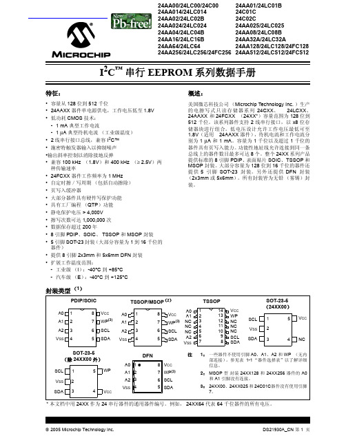
封装类型 (1)
PDIP/SOIC
TSSOP/MSOP(2)
A0 1 A1 2 A2 3 VSS 4
8 VCC
A0 1
7 WP(3) A1 2
6 SCL
A2 3
5 SDA VSS 4
8 VCC
A0 A1
7 WP(3) NC NC
6 SCL NC
5
SDA
A2 VSS
TSSOP
1
14
2
13
3
12
4
11
1.8-5.5V 2.5-5.5V 1.8-5.5V
400 kHz (2)
400 kHz 1 MHz(3)
64 字节
整个阵列
A0, A1, A2(4)
I
P, SN, SM, ST, MS, MF,
I, E ST14
I
256 千位器件
24AA256
1.8-5.5V 400 kHz (2)
24LC256 24FC256
2005 Microchip Technology Inc.
DS21930A_CN 第 3 页
24AAXX/24LCXX/24FCXX
2.0 电气特性
绝对最大额定值 (†)
VCC.............................................................................................................................................................................6.5V 相对于 Vss 的所有输入和输出 ............................................................................................................ -0.6V 到 VCC +1.0V 存储温度 ................................................................................................................................................. -65°C 到 +150°C 环境温度 (使用电源时)........................................................................................................................ -40°C 到 +125°C 所有引脚静电保护 ....................................................................................................................................................................≥ 4 kV
芯片大全
键盘芯片:H8C/2471、H8/3434、H8/3431、PC87570、PC87591
键盘芯片开机功能:H8/3434、H8/3437、H8/2147、H8/2149、H8/2161、H8/2168、PC87570、PC87591、H8S/XXX M38857、M38867、M38869
6030(252封装小的) 7030(263封装大的)
70N03(252封装小的) K3296(263封装大的)
1084(263封装大的) 1117(252封装小的)
75N03(263封装大的) 15N03(252封装小的)
15N03(263封装大的) 45N03(263封装大的)
SC1164/SC1189/SC1185/SC5051/SC1402I/SS93C46-5322-5053
SC1185ACSW/HIP6303/LM2638/LM2637/ST75185C/LM2637M
SC1155/ISL6524/ISL6556BCB/CS5301/ICE2AS01/HIP6620BAB
RT9602/HIP6302/MS-5/MS-7
L6917BD/ISL6556BCB/IRU3013/IRU3055/5090MTC/5093MTC
常用主板场效管,快恢复二极管,特殊电源IC,晶振
3055(252封装小的) 55N03(263封装大的)
55N03(252封装小的) 6030(263封装大的)
PCI系列:PCI4510
SMSC系列:FDC7N869、FDC37N958、LPC47N227、LPC47N26
LPC系列:LPC47N250-SD/LPC47N252-SG/LPC47N254-AQQ/LPC47N253-AQQ/LPC47N249-AQQ
慧聪技术中心文档--Dell QLE2562 SP HBA参考手册
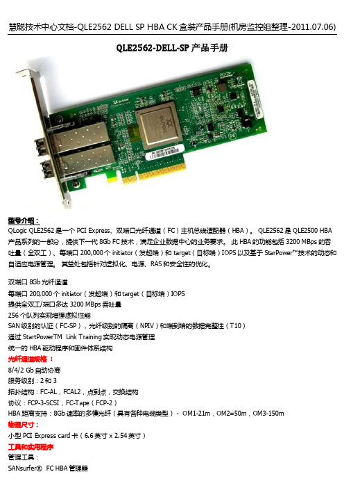
QLE2562-DELL-SP 产品手册型号介绍:QLogic QLE2562是一个PCI Express、双端口光纤通道(FC)主机总线适配器(HBA)。
QLE2562是QLE2500 HBA 产品系列的一部分,提供下一代8Gb FC技术,满足企业数据中心的业务要求。
此HBA的功能包括3200 MBps的吞吐量(全双工)、每端口200,000个initiator(发起端)和target(目标端)IOPS以及基于StarPower™技术的动态和自适应电源管理。
其益处包括针对虚拟化、电源、RAS和安全性的优化。
双端口8Gb光纤通道每端口200,000个initiator(发起端)和target(目标端)IOPS提供全双工/端口多达3200 MBps吞吐量256个队列实现增强虚拟性能SAN级别的认证(FC-SP),光纤级别的隔离(NPIV)和端到端的数据完整性(T10)通过StartPowerTM Link Training实现动态电源管理统一的HBA驱动程序和固件体系结构光纤通道规格 :8/4/2 Gb自动协商服务级别:2和3拓扑结构:FC-AL,FCAL2,点到点,交换结构协议:FCP-3-SCSI,FC-Tape(FCP-2)HBA距离支持:8Gb速率的多模光纤(具有各种电缆类型)- OM1-21m,OM2=50m,OM3-150m物理尺寸:小型PCI Express card卡(6.6英寸 x 2.54英寸)工具和实用程序管理工具:SANsurfer® FC HBA管理器SANsurfer FC HBA CLI设备实用程序:flashing 引导代码实用程序Linux脚本编制工具引导支持:BIOS,Fcode,UEFI,EFIAPI:SNIA HBA API V2,SMI-S,FDMI电源和环境要求电源消耗:6.2瓦(典型)工作温度:0到55摄氏度(32到131华氏度)通风要求:无存储温度:- 40到70摄氏度(-40到158华氏度)相对湿度:10%到90%(运行,无冷凝)和5%到93%(非运行,无冷凝)----------------------------------------------------------------------------------------------------------------------------------管制合规性美国/加拿大:FCC第15部分B子部分A类,ICES-003 A类欧洲:EN55022 A类新西兰/澳大利亚:AS/NZS 3548 A类日本:VCCI V-3/2004.4 A类韩国:MIC台湾:BSMI(CNS 13438)美国/加拿大:安全批准* UL,cUL - UL60950,CSA C22.2 No.60950,符合DHHS 21CFR J的1类激光产品欧洲:安全认证* 73/23/ECC低电压指令* TUV:EN60950-1:2001,EN60825-1:1994+A1+A2,EN60825- 2:1994+A1环境要求符合RoHS 6---------------------------------------------------------------------------------------------------------------------------------- 硬件平台 (x86 and x64)IA32(x86),IA64,Intel- 64AMD-64 Opteron64 (皓龙64)Sun SPARC操作系统支持Windows Server 200,WindowsXP Pro x64,Windows Vista ,Windows Server 2008Linux(Red Hat AS 5.x & 4.x,SLES)Solaris 10 (x86 and SPARC)Vmware ESX/ESXi Server---------------------------------------------------------------------------------------------------------------------------------- 接口标准:PCI-Express Specification rev 2.0接口类型:PCI-E x8模块类型:MMF-SFP-LC附件1: MMF光纤线缆工作模式和传输距离(m)。
常用光电耦合器代换大全
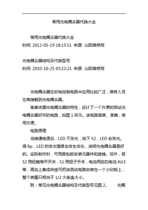
常用光电耦合器代换大全常用光电耦合器代换大全时间: 2012-05-19 18:15:51 来源: 山阳维修网光电耦合器结构及代换型号时间: 2010-10-25 03:22:21 来源: 山阳维修网光电耦合器在彩电控制电路中应用比较广泛,维修人员也常接触到光电耦合器。
笔者依据光电耦合器的特性,设计了一个方便的测试光电耦合器好坏的电路,如图1所示。
该电路简单、准确,使用方便。
电路原理当接通电源后,LED不发光,按下S2,LED会发光。
调Rp,LED的发光强度会发生变化,说明光电耦合器是好的。
实际制作时,可用面包板安装元器件和焊接。
另外,若S2用轻触常开开关,S1用钮子开关,电池用纽扣电池AG3等,再加上集成块座可把该测试电路安装在一个小印板上,整个装置只相当于1/2火柴盒大小。
附:常见光电耦合器结构及代换型号见图2。
光耦合器(opticalcoupler,英文缩写为OC)亦称光电隔离器或光电耦合器,简称光耦。
它是以光为媒介来传输电信号的器件,通常把发光器(红外线发光二极管LED)与受光器(光敏半导体管)封装在同一管壳。
当输入端加电信号时发光器发出光线,受光器接受光线之后就产生光电流,从输出端流出,从而实现了“电—光—电”转换。
以光为媒介把输入端信号耦合到输出端的光电耦合器,由于它具有体积小、寿命长、无触点,抗干扰能力强,输出和输入之间绝缘,单向传输信号等优点,在数字电路上获得广泛的应用。
各品牌光耦替代型号FairchildNECPart NnmberTOSHIBA Par NumberLvPartNnmberTOSHIBA Par Number LvH11A617TLP421BPS2501-1TLP421AH11A817TLP421APS2561-1 TLP421AH11AA814 TLP620BTLP2571-1 TLP421AH11B815 TLP627ATLP2581L1 TLP421F AHMA121 TLP181APS2505-1 TLP620BHMA124 TLP124APS2565-1 TLP620BHMA2701 TLP181APS2502-1 TLP627AHMHA2801 TLP281APS2562-1 TLP627AHMHA281TLP281APS2532-1 TLP627AHMAA2705 TLP180APS2533-1 TLP627HMHAA280 TLP280APS2521-1 TLP629BH11A1 TLP631ATLP2525-1 TLP320BH11AA1 TLP630APS2701-1 TLP181AH11AG1TLP331 APS2761-1 TLP181 AH11B1 TLP571 APS2705-1 TLP180 AH11C1 TLP541G APS2765-1 TLP180 AH11D1 TLP371 CPS2702-1TLP127AH11G1TLP371APS2801-1 TLP281AMOC3021-M TLP3021(S)APS2801-4 TLP281-4AMOC3022-M TLP3022(S) APS2861-1 TLP281AMOC3023-M TLP3023(S) APS2805-1 TLP280AMOC3041-M TLP3041(S) APS2805-4TLP280-4AMOC3042-M TLP3042(S) APS2865-1 TLP280AMOC3043-M TLP3043(S)APS2811-1 TLP283BMOC3051-M TLP3051(S) APS2811-4 TLP283-4BMOC3052-M TLP3052(S) APS8601 TLP759BMOC3061-M TLP3061(S) APS8602 TLP759AMOC3062-M TLP3062(S) APS9613 TLP759(IGM) AMOC3063-M TLP3063(S) APS8701TLP114ABVishayPS8101TLP114ABPart Nnmber TOSHIBA Par Number LvPS9713TLP114A(IGM) BK817PTLP421APS9113TLP114A(IGM) BSFH610ATLP421 APS9601 TLP554 ASFH614A TLP628 APS9614 TLP554SFH615A TLP421 APS9714 TLP115A BSFH617A TLP421 APS9114 TLP115A BSFH618A TLP624 BPS9715 TLP115A BTCET1100TLP421APS9115 TLP115A BSFH690XT TLP181APS9701 TLP115A ATCMT1100 TLP281APS7141-1A TLP597GA ATCMT4100 TLP281-4 APS7141-2ATLP227GA-2 ASFH628A TLP620BPS7141-1B TLP4597G BK815PTLP627APS7141-2B TLP4227G-2 BSFH612A TLP627APS7141-1C TLP4006G BSFH619A TLP627APS7341C-1A TLP594GBSFH655A TLP627APS7141C-2A TLP224G-2BSFH692AT TLP127APS7241-1A TLP176GA ATCED1100 TLP627APS7241-2A TLP206GA AIL66TLP371APS7241-1B TLP4176G BIL66BTLP372APS7241-2B TLP4206G B。
芯片型号
线性稳压块:2951、LP2951、m5236、29500 W- X) H4 j G开机芯片:东芝TM87XX、IBM:TB6805F、TB6806F、TB6808F、TB62501F、TMP48U% L# M1 z7 j) xI/O芯片:PC97338、PC87391、PC87392、pc87393、SMSC系列:FDC7N869、FDC37N958、LPC47N227、LPC47N267% b$ q' g6 F0 m7 i: O9 Y0 M% Y- `2 S系统供电芯片(3.3V和5V电源芯片):MAX1632、MAX1631、MAX1904、MAX1634、MAX785、MAX786、SB3052、SC1402、LTC1628。
7 w" _0 A5 d3 L8 j6 B9 W: a, KCPU供电芯片:MAX1711、MAX1714、MAX1717、MAX1718、MAX18972 _1 {! Y! l+ u- w) b8 e) i/ q. j供电芯片搭配使用:ADP3203/ADP3415、ADP3410/ADP3421、ADP3410/ADP34229 w: P* v% \# C/ D充电芯片:MAX1645、MAX745、MAX1772、MAX1773、ADP3806、TC490/591、MB3887、MB3878、MAX1908 ,LT1505G% A2 H$ H% Q$ l& q) aCPU温度控制芯片:MAX1617、MAX1020A、AD1030A、CM8500 MAX1989" o- c: U C: c: H$ \8 C显卡品牌:A TI、NVIDIA、S3、NEOMAGIC、TRIDENT、SMI、INTEL、FW82807和CH7001A0 J. k( `3 o- p; P0 }6 S搭配使用网卡芯片:RTL8100、RTL8139、Intel DA82562、RC82540、3COM、BCM4409 U! \ j& ?4 l+ O4 v网卡隔离:LF8423、LF-H80P、H-0023、H0024、H0019、ATPL-119 0 m1 L) |5 J+ ~3 S( n6 @; f: e声卡芯片:ESS1921、ESS1980S、STAC9704、AU8810、4299-JQ、TPA0202、4297-JQ、8552TS、8542TS、CS4239-KQ、BA7786、AD1981B、AN12942) {. M) d% [# B8 y3 D. c. V) \. oPC卡芯片:R5C551、R5C552、R5C476、R54472& i5 }0 C) a' R3 e6 b/ H, vPC卡供电芯片:TPS2205、TPS2206、TPS2216、TPS2211、PU2211、M2562A、M2563A、M2564A% [1 w" [. c- ^- M% kCOM口芯片:MAX3243、MAX213、ADM213、HIN213、SP3243、MC145583/ c' k( X2 r" ?. J键盘芯片:H8C/2471、H8/3434、H8/3431、PC87570、PC87591% x7 I, d1 S5 J" O* P键盘芯片:具有开机功能:H8/3434、H8/3437、H8/2147、H8/2149、H8/2161、H8/2168、PC87570、PC87591、H8S/XXX M38857、M38867、M38869; V+ m, V0 L4 g& e5 i( M笔记本IO芯片大全PC87591S(VPCQ01)/PC 87591L(VPC01)/PC 97317IBW/PC 87393 VGJ 2 @) T8 E- g$ w1 K4 n( D- U. K+ K( O+ v3 y. }- H笔记本IO芯片大全TB 62501F/TB62506F/TB6808F/KB910QF/KB910QB4/KB910LQF/KB910LQFA1$ y0 ^: i5 d* U: l5 w7 @; r2 L( l' C0 p# D* s" c, i2 A笔记本IO芯片大全KB3910QB0/KB910SFC1/KB3910SF/PC87591E-VLB/IT8510E/PS51306 G1 H* V2 F# h* U" y' {& v- V% o+ w' j笔记本IO芯片大全PC87591E (-VPCI01),(VPCQ01)/PC 97551-VPC/PC 87570-ICC/VPC5 c E1 n$ {; ?) r' ~7 Y( ?) d E) Z: [4 u) i- A: M( T笔记本IO芯片大全PC87391VGJ/TB6807F/W83L950D/LPC47N249-AQQ/PCI4510/PC8394T8 a# O# H+ @% J4 z' T. R, k, M" O+ N- b O' Y1 V笔记本IO芯片大全PC87392/PC87541L/PC87541V/LPC47N253-AQQ/PC87591E-VLB& A' o7 Q2 b& h& z6 k8 d9 ~2 _( v1 S$ J笔记本IO芯片大全LPC47N250-SD/LPC47N252-SG/LPC47N254-AQQ8 B5 D2 I$ k0 ~" X$ }2 F2 e D0 m很辛苦才记录下来的,我想IBM资料在这个站里应该大多数都有啊,我传也没什么用,想了半天还是想给大家传一个图,T40的图,这个图在我最初学习的时候帮了大忙了,希望也能给大家帮上忙,希望版主在看到我这份诚心上能让我通过啊!!兄弟先谢谢了转载请注明出自中国主板维修基地/,本贴地址:/thread-195179-1-1.html。
EPM2210F256I5N中文资料(Altera)中文数据手册「EasyDatasheet - 矽搜」
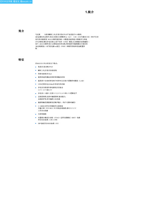
100-Pin FineLine
BGA
100-Pin TQFP
0.5
0.5
1
0.5
25
36
121
256
5×5
6×6
11 × 11 16 × 16
144-Pin TQFP
0.5 484 22 × 22
144-Pin Micro FineLine BGA
256-Pin Micro FineLine BGA
参考文献
本章引用文件下列文件:
■ DC和开关特性
在本章
■ MAX II逻辑单元,以宏单元转换方法
MAX II器件手册
白皮书
文档修订历史记录
表1-6 显示修订历史本章.
表 1-6. 文档修订历史记录
日期和修订
所做更改
2009年8月, 1.9版
2008年10月, 1.8版
2007年12月, version1.7
每一个速度等级和密度范围内数字,指是
特点
在本章
MAX II器件手册.
表1-2 显示MAX II器件速度等级产品.
DC和开关
表 1-2. MAX II速度等级
速度等级
器
EPM240 EPM240G EPM570 EPM570G EPM1270 EPM1270G EPM2210 EPM2210G EPM240Z EPM570Z
特征
在MAX II CPLD具有以下特点: ■ 低成本,低功耗CPLD ■ 瞬时上电,非易失体系结构 ■ 待机电流低至25μA
■ 提供快速传播延迟和时钟到输出时间
■ 提供四个全局时钟有两个时钟可以从每个逻辑阵列模块(LAB) ■ UFM方框多达8 Kbits对非易失性存储
IIC-24LC256系列中文资料

2005 Microchip Technology Inc.
Байду номын сангаас
DS21930A_CN 第 3 页
24AAXX/24LCXX/24FCXX
2.0 电气特性
绝对最大额定值 (†)
VCC.............................................................................................................................................................................6.5V 相对于 Vss 的所有输入和输出 ............................................................................................................ -0.6V 到 VCC +1.0V 存储温度 ................................................................................................................................................. -65°C 到 +150°C 环境温度 (使用电源时)........................................................................................................................ -40°C 到 +125°C 所有引脚静电保护 ....................................................................................................................................................................≥ 4 kV
PS2562L2-1中文资料

DESCRIPTIONThe PS2562-1 is optically coupled isolators containing a GaAs light emitting diode and an NPN silicon darlington connected phototransistor.The PS2562-1 is in a plastic DIP (Dual In-line Package) and the PS2562L-1 is lead bending type (Gull-wing) for surface mount.The PS2562L1-1 is lead bending type for long creepage distance.The PS2562L2-1 is lead bending type for long creepage distance (Gull-wing) for surface mount.FEATURES• High isolation voltage (BV = 5 000 Vr.m.s.) • High current transfer ratio (CTR = 2 000 % TYP.) • High-speed switching (t r , t f = 100 µs TYP.)• Ordering number of tape product: PS2562L-1-E3, E4, F3, F4, PS2562L2-1-E3, E4 • Safety standards • UL approved: File No. E72422 • BSI approved: No. 7112/7420 • CSA approved: No. CA 101391 • NEMKO approved: No. P0******* • SEMKO approved: No. 303059 • DEMKO approved: No. 312341 • FIMKO approved: No. FI 10620• DIN EN60747-5-2 (VDE0884 Part2) approved (option)APPLICATIONS• Power supply • Telephone/FAX. • FA/OA equipment• Programmable logic controllerNEC Compound Semiconductor Devices, Ltd. 1992, 2006DATA SHEETThe information in this document is subject to change without notice. Before using this document, please confirm thatthis is the latest version.Not all devices/types available in every country. Please check with local NEC Compound Semiconductor Devices representative for availability and additional information.The mark shows major revised points.Document No. PN10235EJ03V0DS (3rd edition)Date Published March 2006 CP(K) Printed in JapanPACKAGE DIMENSIONS (UNIT : mm)DIP Type (New package)DIP Type2Data Sheet PN10235EJ03V0DSLead Bending Type (New package)Lead Bending TypeData Sheet PN10235EJ03V0DS3Lead Bending Type For Long Creepage Distance (New Package)Lead Bending Type For Long Creepage Distance4Data Sheet PN10235EJ03V0DSLead Bending Type For Long Creepage Distance (Gull-Wing) (New Package)Lead Bending Type For Long Creepage Distance (Gull-Wing)Data Sheet PN10235EJ03V0DS5MARKING EXAMPLE6Data Sheet PN10235EJ03V0DSORDERING INFORMATIONPart NumberOrder NumberSolder Plating SpecificationPacking StyleSafety StandardApproval Application Part Number *1PS2562-1 PS2562-1-A Pb-Free Magazine case 100 pcs Standard products PS2562-1 PS2562L-1PS2562L-1-A(UL, CSA, BSI, PS2562L1-1 PS2562L1-1-A NEMKO, SEMKO,PS2562L2-1 PS2562L2-1-ADEMKO, FIMKO PS2562L-1-E3 PS2562L-1-E3-A Embossed Tape 1 000 pcs/reel approved) PS2562L-1-E4 PS2562L-1-E4-APS2562L-1-F 3 PS2562L-1-F3-A Embossed Tape 2 000 pcs/reel PS2562L-1-F 4 PS2562L-1-F 4-APS2562L2-1-E3 PS2562L2-1-E3-A Embossed Tape 1 000 pcs/reel PS2562L2-1-E4 PS2562L2-1-E4-APS2562-1-V PS2562-1-V-A Magazine case 100 pcs DIN EN60747-5-2 PS2562L-1-V PS2562L-1-V-A (VDE0884 Part2)PS2562L1-1-V PS2562L1-1-V-A approved products PS2562L2-1-V PS2562L2-1-V-A(option) PS2562L-1-V-E3 PS2562L-1-V-E3-A Embossed Tape 1 000 pcs/reel PS2562L-1-V-E4 PS2562L-1-V-E4-APS2562L-1-V-F 3 PS2562L-1-V-F 3-A Embossed Tape 2 000 pcs/reel PS2562L-1-V-F 4 PS2562L-1-V-F 4-APS2562L2-1-V-E3 PS2562L2-1-V-E3-AEmbossed Tape 1 000 pcs/reel PS2562L2-1-V-E4 PS2562L2-1-V-E4-A*1 For the application of the Safety Standard, following part number should be used.Data Sheet PN10235EJ03V0DS7ABSOLUTE MAXIMUM RATINGS (T A = 25°C, unless otherwise specified)Ratings Unit Parameter SymbolVoltage V R 6 VDiode ReverseForward Current (DC) I F 80 mAPower Dissipation Derating ∆P D/°C 1.5 mW/°CDissipation P D 150 mWPowerPeak Forward Current*1I FP 1 A Transistor Collector to Emitter Voltage V CEO 40 V Emitter to Collector Voltage V ECO 6 VCurrent I C 200 mACollectorPower Dissipation Derating ∆P C/°C 2.0 mW/°CDissipation P C 200 mWPower000Vr.m.s.5Isolation Voltage*2 BVOperating Ambient Temperature T A–55 to +100 °CStorage Temperature T stg–55 to +150 °C*1PW = 100 µs, Duty Cycle = 1%*2AC voltage for 1 minute at T A = 25°C, RH = 60% between input and outputPins 1-2 shorted together, 3-4 shorted together.8Data Sheet PN10235EJ03V0DSELECTRICAL CHARACTERISTICS (T A = 25°C)Parameter Symbol Conditions MIN. TYP. MAX. UnitDiodeorward VoltageV FI F = 10 mA 1.17 1.4 VReverse Current I R V R = 5 V5 µATerminal Capacitance C t V = 0 V, f = 1.0 MHz 50 pF Transistor Collector to Emitter DarkCurrentI CEOV CE = 40 V, I F = 0 mA400nACoupledCurrent Transfer Ratio (I C /I F )*1CTR I F = 1 mA, V CE = 2 V DC 200 2 000 %Collector Saturation VoltageV CE(sat)I F = 1 mA, I C = 2 mA1.0 VIsolation Resistance R I-O V I-O = 1.0 kV DC 1011Ω Isolation Capacitance C I-O V = 0 V, f = 1.0 MHz0.5pFRise Time *2t r V CC = 10 V, I C = 10 mA, R L = 100 Ω 100 µsFall Time *2t f100*1 CTR rank K : 2 000 to (%) L : 700 to 3 400 (%)M : 200 to 1 000 (%)*2 Test circuit for switching timeCCOUTΩData Sheet PN10235EJ03V0DS9TYPICAL CHARACTERISTICS (T A = 25 °C, unless otherwise specified)10075–50–25255075100D i o d e P o w e r D i s s i p a t i o n P D (m W )T r a n s i s t o r P o w e r D i s s i p a t i o n P C (m W )Ambient Temperature T A (˚C)F o r w a r d C u r r e n t I F (m A )Forward Voltage V F (V)C o l l e c t o r C u r r e n tI C (m A )C o l l e c t o r t o E m i t t e rD a r k C u r r e n t I CE O (n A )Collector Saturation Voltage V CE(sat) (V)Ambient Temperature T A (˚C)Ambient Temperature T A (˚C)DIODE POWER DISSIPATION vs.AMBIENT TEMPERATURETRANSISTOR POWER DISSIPATION vs. AMBIENT TEMPERATUREFORWARD CURRENT vs.FORWARD VOLTAGECOLLECTOR CURRENT vs.COLLECTOR TO EMITTER VOLTAGECOLLECTOR TO EMITTER DARKCURRENT vs. AMBIENT TEMPERATUREC o l l e c t o r C u r r e n t I C (m A )0255075100125150Remark The graphs indicate nominal characteristics.Data Sheet PN10235EJ03V0DS101.4251.21.00.80.60.40.2–50–255075100010 k50 k 500100 kNormalized to 1.0at T A = 25 ˚C,I F = 1 mA, V CE = 2 VAmbient Temperature T A (˚C)Load Resistance R L (Ω)Frequency f (kHz)N o r m a l i z e d C u r r e n t T r a n s f e r R a t i o C T RC u r r e n t T r a n s f e r R a t i o C T R (%)N o r m a l i z e d G a i n G VLoad Resistance R L (Ω)S w i t c h i n g T i m e t ( s )µNORMALIZED CURRENT TRANSFER RATIO vs. AMBIENT TEMPERATURECURRENT TRANSFER RATIO vs.FORWARD CURRENTSWITCHING TIME vs.LOAD RESISTANCESWITCHING TIME vs.LOAD RESISTANCES w i t c h i n g T i m e t ( s )µC u r r e n t T r a n s f e r R a t i o C T R (%)Remark The graphs indicate nominal characteristics.Data Sheet PN10235EJ03V0DS116Time (Hr)C T R (R e l a t i v e V a l u e )LONG TERM CTR DEGRADATIONRemark The graph indicates nominal characteristics.Data Sheet PN10235EJ03V0DS12TAPING SPECIFICATIONS (UNIT : mm)Data Sheet PN10235EJ03V0DS1314Data Sheet PN10235EJ03V0DSData Sheet PN10235EJ03V0DS15NOTES ON HANDLING1. Recommended soldering conditions(1) Infrared reflow soldering • Peak reflow temperature 260°C or below (package surface temperature) • Time of peak reflow temperature 10 seconds or less • Time of temperature higher than 220°C 60 seconds or less • Time to preheat temperature from 120 to 180°C 120±30 s• Number of reflows Three• Flux Rosin flux containing small amount of chlorine (The flux with a maximum chlorine content of 0.2 Wt% is recommended.)P a c k a g e S u r f a c e T e m p e r a t u r e T (˚C )Time (s)Recommended Temperature Profile of Infrared Reflow(2) Wave soldering • Temperature 260°C or below (molten solder temperature) • Time10 seconds or less• Preheating conditions 120°C or below (package surface temperature)• Number of times One (Allowed to be dipped in solder including plastic mold portion.)• Flux Rosin flux containing small amount of chlorine (The flux with a maximum chlorine content of 0.2 Wt% is recommended.)(3) Soldering by soldering iron• Peak temperature (lead part temperature) 350°C or below • Time (each pins)3 seconds or less• Flux Rosin flux containing small amount of chlorine (The flux with a maximum chlorine content of 0.2 Wt% is recommended.)(a) Soldering of leads should be made at the point 1.5 to 2.0 mm from the root of the lead. (b) Please be sure that the temperature of the package would not be heated over 100°C.Data Sheet PN10235EJ03V0DS16(4) Cautions• FluxesAvoid removing the residual flux with freon-based and chlorine-based cleaning solvent.2. Cautions regarding noiseBe aware that when voltage is applied suddenly between the photocoupler’s input and output or between collector-emitters at startup, the output transistor may enter the on state, even if the voltage is within the absolute maximum ratings.3. Measurement conditions of current transfer ratios (CTR), which differ according to photocouplerCheck the setting values before use, since the forward current conditions at CTR measurement differ according to product.When using products other than at the specified forward current, the characteristics curves may differ from the standard curves due to CTR value variations or the like. Therefore, check the characteristics under the actual operating conditions and thoroughly take variations or the like into consideration before use.USAGE CAUTIONS1.Protect against static electricity when handling.2.Avoid storage at a high temperature and high humidity.Data Sheet PN10235EJ03V0DS17SPECIFICATION OF VDE MARKS LICENSE DOCUMENTParameter SymbolSpeckUnit Application classification (DIN VDE 0109)for rated line voltages ≤ 300 Vr.m.s. for rated line voltages ≤ 600 Vr.m.s. IV IIIClimatic test class (DIN IEC 68 Teil 1/09.80) 55/100/21 Dielectric strength maximum operating isolation voltageTest voltage (partial discharge test procedure a for type test and random test) U pr = 1.2 × U IORM, P d < 5 pC U IORMU pr8901 068V peakV peakTest voltage (partial discharge test procedure b for all devices test) U pr = 1.6 × U IORM, P d < 5 pC U pr 1424 V peakHighest permissible overvoltage U TR 8000 V peak Degree of pollution (DIN VDE 0109) 2Clearance distance > 7.0 mm Creepage distance > 7.0 mm Comparative tracking index (DIN IEC 112/VDE 0303 part 1) CTI 175Material group (DIN VDE 0109) III aStorage temperature range T stg–55 to +150 °C Operating temperature range T A–55 to +100 °C Isolation resistance, minimum valueV IO = 500 V dc at T A = 25 °CV IO = 500 V dc at T A MAX. at least 100 °C Ris MIN.Ris MIN.10121011ΩΩSafety maximum ratings (maximum permissible in case of fault, see thermal derating curve)Package temperatureCurrent (input current I F, Psi = 0)Power (output or total power dissipation) Isolation resistanceV IO = 500 V dc at T A = 175 °C (Tsi)TsiIsiPsiRis MIN.175400700109°CmAmWΩData Sheet PN10235EJ03V0DS18When the product(s) listed in this document is subject to any applicable import or export control laws and regulation of the authority having competent jurisdiction, such product(s) shall not be imported or exported without obtaining the import or export license.M8E 00. 4 - 0110The information in this document is current as of March, 2006. The information is subject to changewithout notice. For actual design-in, refer to the latest publications of NEC's data sheets or data books, etc., for the most up-to-date specifications of NEC semiconductor products. Not all products and/or types are available in every country. Please check with an NEC sales representative for availability and additional information.No part of this document may be copied or reproduced in any form or by any means without prior written consent of NEC. NEC assumes no responsibility for any errors that may appear in this document.NEC does not assume any liability for infringement of patents, copyrights or other intellectual property rights of third parties by or arising from the use of NEC semiconductor products listed in this document or any other liability arising from the use of such products. No license, express, implied or otherwise, is granted under any patents, copyrights or other intellectual property rights of NEC or others.Descriptions of circuits, software and other related information in this document are provided for illustrative purposes in semiconductor product operation and application examples. The incorporation of these circuits, software and information in the design of customer's equipment shall be done under the full responsibility of customer. NEC assumes no responsibility for any losses incurred by customers or third parties arising from the use of these circuits, software and information.While NEC endeavours to enhance the quality, reliability and safety of NEC semiconductor products, customers agree and acknowledge that the possibility of defects thereof cannot be eliminated entirely. To minimize risks of damage to property or injury (including death) to persons arising from defects in NEC semiconductor products, customers must incorporate sufficient safety measures in their design, such as redundancy, fire-containment, and anti-failure features.NEC semiconductor products are classified into the following three quality grades:"Standard", "Special" and "Specific". The "Specific" quality grade applies only to semiconductor products developed based on a customer-designated "quality assurance program" for a specific application. The recommended applications of a semiconductor product depend on its quality grade, as indicated below. Customers must check the quality grade of each semiconductor product before using it in a particular application."Standard":Computers, office equipment, communications equipment, test and measurement equipment, audioand visual equipment, home electronic appliances, machine tools, personal electronic equipment and industrial robots"Special":Transportation equipment (automobiles, trains, ships, etc.), traffic control systems, anti-disastersystems, anti-crime systems, safety equipment and medical equipment (not specifically designed for life support)"Specific":Aircraft, aerospace equipment, submersible repeaters, nuclear reactor control systems, lifesupport systems and medical equipment for life support, etc.The quality grade of NEC semiconductor products is "Standard" unless otherwise expressly specified in NEC's data sheets or data books, etc. If customers wish to use NEC semiconductor products in applications not intended by NEC, they must contact an NEC sales representative in advance to determine NEC's willingness to support a given application.(Note)(1)"NEC" as used in this statement means NEC Corporation, NEC Compound Semiconductor Devices, Ltd.and also includes its majority-owned subsidiaries.(2)"NEC semiconductor products" means any semiconductor product developed or manufactured by or forNEC (as defined above).••••••Data Sheet PN10235EJ03V0DS19NEC Compound Semiconductor Devices Hong Kong Limited E-mail: ncsd-hk@ (sales, technical and general)Hong Kong Head Office T aipei Branch OfficeKorea Branch OfficeTEL: +852-3107-7303TEL: +886-2-8712-0478TEL: +82-2-558-2120FAX: +852-3107-7309 FAX: +886-2-2545-3859FAX: +82-2-558-5209NEC Electronics (Europe) GmbH http://www.ee.nec.de/TEL: +49-211-6503-0 FAX: +49-211-6503-1327California Eastern Laboratories, Inc. / TEL: +1-408-988-3500 FAX: +1-408-988-02790504NEC Compound Semiconductor Devices, Ltd. / E-mail: salesinfo@ (sales and general) techinfo@ (technical)Sales Division TEL: +81-44-435-1573 FAX: +81-44-435-1579For further information, please contact。
2P4M中文资料(nec)中文数据手册「EasyDatasheet - 矽搜」

热阻
Rt h(j-c )
结到外壳DC
−
−
10 °C/W 参照图11
Rt h(j-a)
结到环境DC
−
−
75
Note 插入阻力门极和阴极之间的低于1kΩ,因为显示的项都受到保障
连接门极和阴极(R之间的短期阻力
GK = 1 kΩ).
2
Data Sheet D13531EJ5V0DS
芯片中文手册,看全文,戳
−
门非触发电压
Note
VGD VDM = 1/2 V DRM , Tj = 125°C,
0.2
TYP. MAX. UNIT 备注
−
10
μA
−
−
100
−
−
10
μA
−
−
100
−
−
−
V/μs 2P4M
10
−
2P6M
−
2.2
V 参照图1
−
200
μA 参照图5,
图. 7
−
0.8
V 参照图6,
图. 8
−
−
V
−
保持电流
“专业”:运输设备(汽车,火车,船舶等),交通控制系统,防灾 系统,反犯罪系统,安全设备和医疗设备(不包括专门为生命而设计的).
“特殊”:飞机,航空设备,水下中继器,核反应堆控制系统,生命
支持系统和生命支持等医疗设备
文所定义).
M8E 02. 11-1
典型特征(T
A = 25°C)
2P4M,2P6M
3
Data Sheet D13531EJ5V0DS
芯片中文手册,看全文,戳
2P4M,2P6M
奥伦德光耦产品对比表V3.1

LTV-824
LTV-844 LTV-214 LTV-354T
LTV-815 LTV-825 LTV-845 LTV-215
PS2702-1
LTV-355T
EL EL817
EL827 EL847 EL3H7 EL357
EL816 EL10XX
4N3X H11AX 4N2X H11AX EL814
消除地面回路,LSTTL to TTL,LSTTL or 5 volt CMOS 线接收器,数据 传输,开关电源,脉冲变压器更换,计算机外设接口,地面高速
逻辑隔离
TYPE
ORIENT AVAGO FAIRCHILD TOSHIBA
OR817 HCPL-817
H11A817 FOD817
TLP521-1
股票代码:832016
深圳奥伦德依托 20 多年积累的红外芯片技术,深耕光电耦合器十余载,是大陆首家通过 VDE、UL、CQC 认证并 量产化的企业。我司光耦产品伴随几百家客户 10 多年来一起成长,积累销售光耦近百亿只,产品走入千家万户。 作为一种安全器件,为广大用户提供了保证。是国内公认的历史最久、产能最大、型号最全的光耦芯片及封装研发 和生产基地。
SHARP
RENESA
VISHAY
LITEON
EL
COSMO
OR301X OR302X OR304X OR305X
OR306X
OR308X
Thyristor
MOC302X
MOC304X
MOC305X
MOC306X
OR155E
ORM501
ORM600
ORM601
ORM611
High-speed
2562中文资料

Mechanical and Magnetic Data
● Maximum primary power: 200 W @ 100 kHz
● Slot technology, Lizt wire recommended for proximity and skin effects reduction
● Mains insulation according to IEC60065 and IEC60950 safety standards
9+9 6+6 6+6 8+8 7+7 9+9 9+9 7+7 11 +11 6+6 6+6
6+6
4+4 6+6 9+9 4+4 5+4 4+4 4+4 5+5 5+5 5+5 5+5 5+5 7+7
Slot Slot Slot Slot Slot Slot Slot Slot Slot Slot
Layer Layer Layer Layer Layer Layer Layer Layer Layer Layer Layer
LCD TV 37"-42"
Battery chargers LCD 22" Satellite receiver Battery chargers, stand-by circuits, white goods Battery chargers, stand-by circuits, white goods Battery chargers, stand-by circuits, Set-top Box Not mains insulated SMT Battery chargers, stand-by circuits, Set-top Box Battery chargers, stand-by circuits, Set-top Box Set-top Box, White goods DVD, satellite receiver DVD, satellite receiver for slim version DVD, satellite receiver for slim version
常用内存命名规则

常见内存芯片命名2010-06-08 21:13:23| 分类:个人日记| 标签:|字号大中小订阅三星(Samsung)内存具体含义解释:例:SAMSUNGK4S283232E-TC60 SDRAMK4H280838B-TCB0 DDRK4T51163QE-HCE6 DDR2K4B1G164E-HCE7 DDR3主要含义:第1位——芯片功能K,代表是内存芯片。
第2位——芯片类型4,代表DRAM。
9代表NAND FLASH第3位——芯片的更进一步的类型说明,S代表SDRAM、H代表DDR、T代表DDR2、B代表DDR3、G代表SGRAM。
第4、5位——容量和刷新速率,容量相同的内存采用不同的刷新速率,也会使用不同的编号。
64、62、63、65、66、67、6A代表64Mbit的容量;28、27、2A 代表128Mbit的容量;56、55、57、5A代表256Mbit的容量;51代表512Mbit 的容量。
第6、7位——数据线引脚个数,08代表8位数据;16代表16位数据;32代表32位数据;64代表64位数据。
第11位——连线“-”。
第14、15位——芯片的速率,如60为6ns;70为7ns;7B为7.5ns(CL=3);7C 为7.5ns(CL=2);80为8ns;10为10ns(66MHz)。
知道了内存颗粒编码主要数位的含义,拿到一个内存条后就非常容易计算出它的容量。
例如一条三星DDR内存,使用18片SAMSUNGK4H280838B-TCB0颗粒封装。
颗粒编号第4、5位“28”代表该颗粒是128Mbits,第6、7位“08”代表该颗粒是8位数据带宽,这样我们可以计算出该内存条的容量是128Mbits(兆数位)×16片/8bits=256MB(兆字节)。
注:“bit”为“数位”,“B”即字节“byte”,一个字节为8位则计算时除以8。
关于内存容量的计算,文中所举的例子中有两种情况:一种是非ECC内存,每8片8位数据宽度的颗粒就可以组成一条内存;另一种ECC内存,在每64位数据之后,还增加了8位的ECC校验码。
船舶规范中英文对照

船舶规范-中英对照、CARGO GEAR: d文,wen,从玄从爻。
天地万物的信息产生出来的现象、纹路、轨迹,描绘出了阴阳二气在事物中的运行轨迹和原理。
故文即为符。
上古之时,符文一体。
古者伏羲氏之王天下也,始画八卦,造书契,以代结绳(爻)之政,由是文籍生焉。
--《尚书序》依类象形,故谓之文。
其后形声相益,即谓之字。
--《说文》序》仓颉造书,形立谓之文,声具谓之字。
--《古今通论》(1) 象形。
甲骨文此字象纹理纵横交错形。
"文"是汉字的一个部首。
本义:花纹;纹理。
(2) 同本义[figure;veins]文,英语念为:text、article等,从字面意思上就可以理解为文章、文字,与古今中外的各个文学著作中出现的各种文字字形密不可分。
古有甲骨文、金文、小篆等,今有宋体、楷体等,都在这一方面突出了"文"的重要性。
古今中外,人们对于"文"都有自己不同的认知,从大的方面来讲,它可以用于表示一个民族的文化历史,从小的方面来说它可用于用于表示单独的一个"文"字,可用于表示一段话,也可用于人物的姓氏。
折叠编辑本段基本字义1.事物错综所造成的纹理或形象:灿若~锦。
2.刺画花纹:~身。
3.记录语言的符号:~字。
~盲。
以~害辞。
4.用文字记下来以及与之有关的:~凭。
~艺。
~体。
~典。
~苑。
~献(指有历史价值和参考价值的图书资料)。
~采(a.文辞、文艺方面的才华;b.错杂艳丽的色彩)。
5.人类劳动成果的总结:~化。
~物。
6.自然界的某些现象:天~。
水~。
7.旧时指礼节仪式:虚~。
繁~缛节(过多的礼节仪式)。
8.文华辞采,与“质”、“情”相对:~质彬彬。
9.温和:~火。
~静。
~雅。
10.指非军事的:~职。
~治武功(指礼乐教化和军事功绩)。
11.指以古汉语为基础的书面语:552~言。
~白间杂。
12.专指社会科学:~科。
13.掩饰:~过饰非。
14.量词,指旧时小铜钱:一~不名。
X25-E技术规格

MEMORY存储芯片N25Q128A11E1241E中文规格书
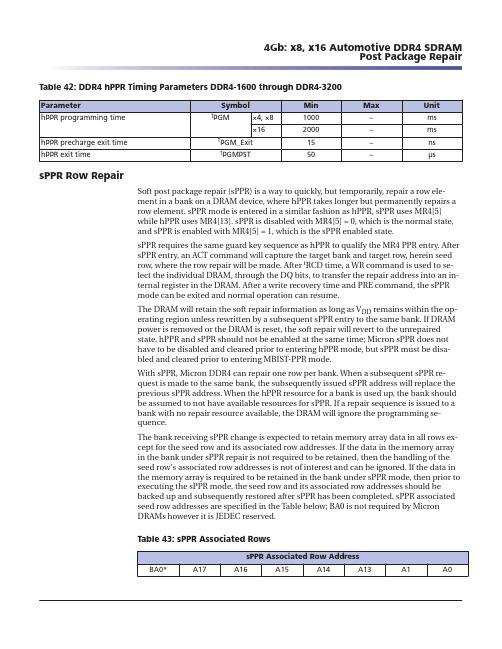
Table 42: DDR4 hPPR Timing Parameters DDR4-1600 through DDR4-3200sPPR Row RepairSoft post package repair (sPPR) is a way to quickly, but temporarily, repair a row ele-ment in a bank on a DRAM device, where hPPR takes longer but permanently repairs a row element. sPPR mode is entered in a similar fashion as hPPR, sPPR uses MR4[5]while hPPR uses MR4[13]. sPPR is disabled with MR4[5] = 0, which is the normal state,and sPPR is enabled with MR4[5] = 1, which is the sPPR enabled state.sPPR requires the same guard key sequence as hPPR to qualify the MR4 PPR entry. After sPPR entry, an ACT command will capture the target bank and target row, herein seed row, where the row repair will be made. After t RCD time, a WR command is used to se-lect the individual DRAM, through the DQ bits, to transfer the repair address into an in-ternal register in the DRAM. After a write recovery time and PRE command, the sPPR mode can be exited and normal operation can resume.The DRAM will retain the soft repair information as long as V DD remains within the op-erating region unless rewritten by a subsequent sPPR entry to the same bank. If DRAM power is removed or the DRAM is reset, the soft repair will revert to the unrepaired state. hPPR and sPPR should not be enabled at the same time; Micron sPPR does not have to be disabled and cleared prior to entering hPPR mode, but sPPR must be disa-bled and cleared prior to entering MBIST-PPR mode.With sPPR, Micron DDR4 can repair one row per bank. When a subsequent sPPR re-quest is made to the same bank, the subsequently issued sPPR address will replace the previous sPPR address. When the hPPR resource for a bank is used up, the bank should be assumed to not have available resources for sPPR. If a repair sequence is issued to a bank with no repair resource available, the DRAM will ignore the programming se-quence.The bank receiving sPPR change is expected to retain memory array data in all rows ex-cept for the seed row and its associated row addresses. If the data in the memory array in the bank under sPPR repair is not required to be retained, then the handling of the seed row’s associated row addresses is not of interest and can be ignored. If the data in the memory array is required to be retained in the bank under sPPR mode, then prior to executing the sPPR mode, the seed row and its associated row addresses should be backed up and subsequently restored after sPPR has been completed. sPPR associated seed row addresses are specified in the Table below; BA0 is not required by Micron DRAMs however it is JEDEC reserved.Table 43: sPPR Associated Rows4Gb: x8, x16 Automotive DDR4 SDRAM Post Package Repairvalue may not be exactly within the voltage range setting coupled with the V REF set tol-erance; the device must be calibrated to the correct internal V REFDQ voltage.Figure 64: Example of V REF Set Tolerance and Step SizeV REFDigital CodeNote: 1.Maximum case shown.V REFDQ Increment and Decrement TimingThe V REF increment/decrement step times are defined by V REF,time. V REF,time is definedfrom t0 to t1, where t1 is referenced to the V REF voltage at the final DC level within theV REF valid tolerance (V REF,val_tol). The V REF valid level is defined by V REF,val tolerance toqualify the step time t1. This parameter is used to insure an adequate RC time constantbehavior of the voltage level change after any V REF increment/decrement adjustment.Logic Equations for a x8 DeviceDQ0 = MT0DQ5 = MT5DQ1 = MT1DQ6 = MT6DQ2 = MT2DQ7 = MT7DQ3 = MT3DQS_t = MT8DQ4 = MT4DQS_c = MT9Logic Equations for a x16 DeviceDQ0 = MT0DQ10 = INV DQ2DQ1 = MT1DQ11 = INV DQ3DQ2 = MT2DQ12 = INV DQ4DQ3 = MT3DQ13 = INV DQ5DQ4 = MT4DQ14 = INV DQ6DQ5 = MT5DQ15 = INV DQ7DQ6 = MT6LDQS_t = MT8DQ7 = MT7LDQS_c = MT9DQ8 = INV DQ0UDQS_t = INV LDQS_tDQ9 = INV DQ1UDQS_c = INV LDQS_cCT Input Timing RequirementsPrior to the assertion of the TEN pin, all voltage supplies, including V REFCA, must be val-id and stable and RESET_n registered high prior to entering CT mode. Upon the asser-tion of the TEN pin HIGH with RESET_n, CKE, and CS_n held HIGH; CLK_t, CLK_c, andCKE signals become test inputs within t CTECT_Valid. The remaining CT inputs becomevalid t CT_Enable after TEN goes HIGH when CS_n allows input to begin sampling, pro-vided inputs were valid for at least t CT_Valid. While in CT mode, refresh activities in thememory arrays are not allowed; they are initiated either externally (auto refresh) or in-ternally (self refresh).The TEN pin may be asserted after the DRAM has completed power-on. After the DRAMis initialized and V REFDQ is calibrated, CT mode may no longer be used. The TEN pinmay be de-asserted at any time in CT mode. Upon exiting CT mode, the states and theintegrity of the original content of the memory array are unknown. A full reset of thememory device is required.After CT mode has been entered, the output signals will be stable within t CT_Valid afterthe test inputs have been applied as long as TEN is maintained HIGH and CS_n is main-tained LOW.。
7款中端固态硬盘年度横评
泰国洪水铸就固态硬盘崛起泰国洪水改变了机械硬盘格局,同时也改变了固态硬盘的命运。
中关村卖场每每新到一批固态硬盘,在短短数天即销售告罄,而固态硬盘厂家在第三季度的营收翻倍,固态硬盘出现产销两旺的局面。
它到底有什么魔力让消费者如此青睐,就连造内存起家的金士顿也厚积薄发推出骇客系列高端固态硬盘呢?机械硬盘曾以“高容价比和高性价比”这两大优势占领硬盘市场,随着泰国洪水的冲根本原因。
速度超越500MB/秒 7款大容量固态硬盘横向评测固态硬盘市场和传统的机械硬盘市场并不相同。
目前机械硬盘品牌主要有三巨头把持,同时它们之间的产品性能都差别不大,消费者在购买时很容易选择。
而固态硬盘则不同,目前市场上光是不同的主控方案就有五种以上,品牌更是有几十个,而且它们之间的性能和价格差距都非常大,这就导致了许多消费者在购买时无从下手。
今天笔者就为拥有SATA3.0平台的用户选择了7款高速度大容量固态硬盘,分属Marvell、SandForce、Samsung三大派系的主控芯片,对它们进行横向对比,看看哪款更适合您。
相关阅读:<硬盘大幅涨年底装机选择SSD的4大理由>金士顿HyperX 240GB固态硬盘简介★金士顿HyperX 240GB固态硬盘简介HyperX是金士顿独有的高端产品系列,象征超越无极限,其中以蓝色散热片的HyperX 超频内存最为玩家所津津乐道。
今年金士顿HyperX高端产品线再添举足轻重的新成员,它就是金士顿HyperX固态硬盘。
金士顿HyperX 240GB固态硬盘正面特写金士顿HyperX 240GB固态硬盘的份量和SSDnow系列一样足,注重对盘体的保护,内衬有软胶粘覆在PCB板一侧进行缓冲保护。
它采用铝合金底壳,提供坚固外壳保护和良好的散热效能。
其正面覆盖一层蓝色的ABS工程塑料外壳,表面分布均匀着大小一致的散热孔,灰色的铝合金散热器与之粘合加强散热。
正面铝合金外壳刻印有HYPERX的英文字母和金士顿的英文LOGO。
- 1、下载文档前请自行甄别文档内容的完整性,平台不提供额外的编辑、内容补充、找答案等附加服务。
- 2、"仅部分预览"的文档,不可在线预览部分如存在完整性等问题,可反馈申请退款(可完整预览的文档不适用该条件!)。
- 3、如文档侵犯您的权益,请联系客服反馈,我们会尽快为您处理(人工客服工作时间:9:00-18:30)。
DESCRIPTIONThe PS2562-1 is optically coupled isolators containing a GaAs light emitting diode and an NPN silicon darlington connected phototransistor.The PS2562-1 is in a plastic DIP (Dual In-line Package) and the PS2562L-1 is lead bending type (Gull-wing) for surface mount.The PS2562L1-1 is lead bending type for long creepage distance.The PS2562L2-1 is lead bending type for long creepage distance (Gull-wing) for surface mount.FEATURES• High isolation voltage (BV = 5 000 Vr.m.s.) • High current transfer ratio (CTR = 2 000 % TYP.) • High-speed switching (t r , t f = 100 µs TYP.)• Ordering number of tape product: PS2562L-1-E3, E4, F3, F4, PS2562L2-1-E3, E4 • Safety standards • UL approved: File No. E72422 • BSI approved: No. 7112/7420 • CSA approved: No. CA 101391 • NEMKO approved: No. P0******* • SEMKO approved: No. 303059 • DEMKO approved: No. 312341 • FIMKO approved: No. FI 10620• DIN EN60747-5-2 (VDE0884 Part2) approved (option)APPLICATIONS• Power supply • Telephone/FAX. • FA/OA equipment• Programmable logic controllerNEC Compound Semiconductor Devices, Ltd. 1992, 2006DATA SHEETThe information in this document is subject to change without notice. Before using this document, please confirm thatthis is the latest version.Not all devices/types available in every country. Please check with local NEC Compound Semiconductor Devices representative for availability and additional information.The mark shows major revised points.Document No. PN10235EJ03V0DS (3rd edition)Date Published March 2006 CP(K) Printed in JapanPACKAGE DIMENSIONS (UNIT : mm)DIP Type (New package)DIP Type2Data Sheet PN10235EJ03V0DSLead Bending Type (New package)Lead Bending TypeData Sheet PN10235EJ03V0DS3Lead Bending Type For Long Creepage Distance (New Package)Lead Bending Type For Long Creepage Distance4Data Sheet PN10235EJ03V0DSLead Bending Type For Long Creepage Distance (Gull-Wing) (New Package)Lead Bending Type For Long Creepage Distance (Gull-Wing)Data Sheet PN10235EJ03V0DS5MARKING EXAMPLE6Data Sheet PN10235EJ03V0DSORDERING INFORMATIONPart NumberOrder NumberSolder Plating SpecificationPacking StyleSafety StandardApproval Application Part Number *1PS2562-1 PS2562-1-A Pb-Free Magazine case 100 pcs Standard products PS2562-1 PS2562L-1PS2562L-1-A(UL, CSA, BSI, PS2562L1-1 PS2562L1-1-A NEMKO, SEMKO,PS2562L2-1 PS2562L2-1-ADEMKO, FIMKO PS2562L-1-E3 PS2562L-1-E3-A Embossed Tape 1 000 pcs/reel approved) PS2562L-1-E4 PS2562L-1-E4-APS2562L-1-F 3 PS2562L-1-F3-A Embossed Tape 2 000 pcs/reel PS2562L-1-F 4 PS2562L-1-F 4-APS2562L2-1-E3 PS2562L2-1-E3-A Embossed Tape 1 000 pcs/reel PS2562L2-1-E4 PS2562L2-1-E4-APS2562-1-V PS2562-1-V-A Magazine case 100 pcs DIN EN60747-5-2 PS2562L-1-V PS2562L-1-V-A (VDE0884 Part2)PS2562L1-1-V PS2562L1-1-V-A approved products PS2562L2-1-V PS2562L2-1-V-A(option) PS2562L-1-V-E3 PS2562L-1-V-E3-A Embossed Tape 1 000 pcs/reel PS2562L-1-V-E4 PS2562L-1-V-E4-APS2562L-1-V-F 3 PS2562L-1-V-F 3-A Embossed Tape 2 000 pcs/reel PS2562L-1-V-F 4 PS2562L-1-V-F 4-APS2562L2-1-V-E3 PS2562L2-1-V-E3-AEmbossed Tape 1 000 pcs/reel PS2562L2-1-V-E4 PS2562L2-1-V-E4-A*1 For the application of the Safety Standard, following part number should be used.Data Sheet PN10235EJ03V0DS7ABSOLUTE MAXIMUM RATINGS (T A = 25°C, unless otherwise specified)Ratings Unit Parameter SymbolVoltage V R 6 VDiode ReverseForward Current (DC) I F 80 mAPower Dissipation Derating ∆P D/°C 1.5 mW/°CDissipation P D 150 mWPowerPeak Forward Current*1I FP 1 A Transistor Collector to Emitter Voltage V CEO 40 V Emitter to Collector Voltage V ECO 6 VCurrent I C 200 mACollectorPower Dissipation Derating ∆P C/°C 2.0 mW/°CDissipation P C 200 mWPower000Vr.m.s.5Isolation Voltage*2 BVOperating Ambient Temperature T A–55 to +100 °CStorage Temperature T stg–55 to +150 °C*1PW = 100 µs, Duty Cycle = 1%*2AC voltage for 1 minute at T A = 25°C, RH = 60% between input and outputPins 1-2 shorted together, 3-4 shorted together.8Data Sheet PN10235EJ03V0DSELECTRICAL CHARACTERISTICS (T A = 25°C)Parameter Symbol Conditions MIN. TYP. MAX. UnitDiodeorward VoltageV FI F = 10 mA 1.17 1.4 VReverse Current I R V R = 5 V5 µATerminal Capacitance C t V = 0 V, f = 1.0 MHz 50 pF Transistor Collector to Emitter DarkCurrentI CEOV CE = 40 V, I F = 0 mA400nACoupledCurrent Transfer Ratio (I C /I F )*1CTR I F = 1 mA, V CE = 2 V DC 200 2 000 %Collector Saturation VoltageV CE(sat)I F = 1 mA, I C = 2 mA1.0 VIsolation Resistance R I-O V I-O = 1.0 kV DC 1011Ω Isolation Capacitance C I-O V = 0 V, f = 1.0 MHz0.5pFRise Time *2t r V CC = 10 V, I C = 10 mA, R L = 100 Ω 100 µsFall Time *2t f100*1 CTR rank K : 2 000 to (%) L : 700 to 3 400 (%)M : 200 to 1 000 (%)*2 Test circuit for switching timeCCOUTΩData Sheet PN10235EJ03V0DS9TYPICAL CHARACTERISTICS (T A = 25 °C, unless otherwise specified)10075–50–25255075100D i o d e P o w e r D i s s i p a t i o n P D (m W )T r a n s i s t o r P o w e r D i s s i p a t i o n P C (m W )Ambient Temperature T A (˚C)F o r w a r d C u r r e n t I F (m A )Forward Voltage V F (V)C o l l e c t o r C u r r e n tI C (m A )C o l l e c t o r t o E m i t t e rD a r k C u r r e n t I CE O (n A )Collector Saturation Voltage V CE(sat) (V)Ambient Temperature T A (˚C)Ambient Temperature T A (˚C)DIODE POWER DISSIPATION vs.AMBIENT TEMPERATURETRANSISTOR POWER DISSIPATION vs. AMBIENT TEMPERATUREFORWARD CURRENT vs.FORWARD VOLTAGECOLLECTOR CURRENT vs.COLLECTOR TO EMITTER VOLTAGECOLLECTOR TO EMITTER DARKCURRENT vs. AMBIENT TEMPERATUREC o l l e c t o r C u r r e n t I C (m A )0255075100125150Remark The graphs indicate nominal characteristics.Data Sheet PN10235EJ03V0DS101.4251.21.00.80.60.40.2–50–255075100010 k50 k 500100 kNormalized to 1.0at T A = 25 ˚C,I F = 1 mA, V CE = 2 VAmbient Temperature T A (˚C)Load Resistance R L (Ω)Frequency f (kHz)N o r m a l i z e d C u r r e n t T r a n s f e r R a t i o C T RC u r r e n t T r a n s f e r R a t i o C T R (%)N o r m a l i z e d G a i n G VLoad Resistance R L (Ω)S w i t c h i n g T i m e t ( s )µNORMALIZED CURRENT TRANSFER RATIO vs. AMBIENT TEMPERATURECURRENT TRANSFER RATIO vs.FORWARD CURRENTSWITCHING TIME vs.LOAD RESISTANCESWITCHING TIME vs.LOAD RESISTANCES w i t c h i n g T i m e t ( s )µC u r r e n t T r a n s f e r R a t i o C T R (%)Remark The graphs indicate nominal characteristics.Data Sheet PN10235EJ03V0DS116Time (Hr)C T R (R e l a t i v e V a l u e )LONG TERM CTR DEGRADATIONRemark The graph indicates nominal characteristics.Data Sheet PN10235EJ03V0DS12TAPING SPECIFICATIONS (UNIT : mm)Data Sheet PN10235EJ03V0DS1314Data Sheet PN10235EJ03V0DSData Sheet PN10235EJ03V0DS15NOTES ON HANDLING1. Recommended soldering conditions(1) Infrared reflow soldering • Peak reflow temperature 260°C or below (package surface temperature) • Time of peak reflow temperature 10 seconds or less • Time of temperature higher than 220°C 60 seconds or less • Time to preheat temperature from 120 to 180°C 120±30 s• Number of reflows Three• Flux Rosin flux containing small amount of chlorine (The flux with a maximum chlorine content of 0.2 Wt% is recommended.)P a c k a g e S u r f a c e T e m p e r a t u r e T (˚C )Time (s)Recommended Temperature Profile of Infrared Reflow(2) Wave soldering • Temperature 260°C or below (molten solder temperature) • Time10 seconds or less• Preheating conditions 120°C or below (package surface temperature)• Number of times One (Allowed to be dipped in solder including plastic mold portion.)• Flux Rosin flux containing small amount of chlorine (The flux with a maximum chlorine content of 0.2 Wt% is recommended.)(3) Soldering by soldering iron• Peak temperature (lead part temperature) 350°C or below • Time (each pins)3 seconds or less• Flux Rosin flux containing small amount of chlorine (The flux with a maximum chlorine content of 0.2 Wt% is recommended.)(a) Soldering of leads should be made at the point 1.5 to 2.0 mm from the root of the lead. (b) Please be sure that the temperature of the package would not be heated over 100°C.Data Sheet PN10235EJ03V0DS16(4) Cautions• FluxesAvoid removing the residual flux with freon-based and chlorine-based cleaning solvent.2. Cautions regarding noiseBe aware that when voltage is applied suddenly between the photocoupler’s input and output or between collector-emitters at startup, the output transistor may enter the on state, even if the voltage is within the absolute maximum ratings.3. Measurement conditions of current transfer ratios (CTR), which differ according to photocouplerCheck the setting values before use, since the forward current conditions at CTR measurement differ according to product.When using products other than at the specified forward current, the characteristics curves may differ from the standard curves due to CTR value variations or the like. Therefore, check the characteristics under the actual operating conditions and thoroughly take variations or the like into consideration before use.USAGE CAUTIONS1.Protect against static electricity when handling.2.Avoid storage at a high temperature and high humidity.Data Sheet PN10235EJ03V0DS17SPECIFICATION OF VDE MARKS LICENSE DOCUMENTParameter SymbolSpeckUnit Application classification (DIN VDE 0109)for rated line voltages ≤ 300 Vr.m.s. for rated line voltages ≤ 600 Vr.m.s. IV IIIClimatic test class (DIN IEC 68 Teil 1/09.80) 55/100/21 Dielectric strength maximum operating isolation voltageTest voltage (partial discharge test procedure a for type test and random test) U pr = 1.2 × U IORM, P d < 5 pC U IORMU pr8901 068V peakV peakTest voltage (partial discharge test procedure b for all devices test) U pr = 1.6 × U IORM, P d < 5 pC U pr 1424 V peakHighest permissible overvoltage U TR 8000 V peak Degree of pollution (DIN VDE 0109) 2Clearance distance > 7.0 mm Creepage distance > 7.0 mm Comparative tracking index (DIN IEC 112/VDE 0303 part 1) CTI 175Material group (DIN VDE 0109) III aStorage temperature range T stg–55 to +150 °C Operating temperature range T A–55 to +100 °C Isolation resistance, minimum valueV IO = 500 V dc at T A = 25 °CV IO = 500 V dc at T A MAX. at least 100 °C Ris MIN.Ris MIN.10121011ΩΩSafety maximum ratings (maximum permissible in case of fault, see thermal derating curve)Package temperatureCurrent (input current I F, Psi = 0)Power (output or total power dissipation) Isolation resistanceV IO = 500 V dc at T A = 175 °C (Tsi)TsiIsiPsiRis MIN.175400700109°CmAmWΩData Sheet PN10235EJ03V0DS18When the product(s) listed in this document is subject to any applicable import or export control laws and regulation of the authority having competent jurisdiction, such product(s) shall not be imported or exported without obtaining the import or export license.M8E 00. 4 - 0110The information in this document is current as of March, 2006. The information is subject to changewithout notice. For actual design-in, refer to the latest publications of NEC's data sheets or data books, etc., for the most up-to-date specifications of NEC semiconductor products. Not all products and/or types are available in every country. Please check with an NEC sales representative for availability and additional information.No part of this document may be copied or reproduced in any form or by any means without prior written consent of NEC. NEC assumes no responsibility for any errors that may appear in this document.NEC does not assume any liability for infringement of patents, copyrights or other intellectual property rights of third parties by or arising from the use of NEC semiconductor products listed in this document or any other liability arising from the use of such products. No license, express, implied or otherwise, is granted under any patents, copyrights or other intellectual property rights of NEC or others.Descriptions of circuits, software and other related information in this document are provided for illustrative purposes in semiconductor product operation and application examples. The incorporation of these circuits, software and information in the design of customer's equipment shall be done under the full responsibility of customer. NEC assumes no responsibility for any losses incurred by customers or third parties arising from the use of these circuits, software and information.While NEC endeavours to enhance the quality, reliability and safety of NEC semiconductor products, customers agree and acknowledge that the possibility of defects thereof cannot be eliminated entirely. To minimize risks of damage to property or injury (including death) to persons arising from defects in NEC semiconductor products, customers must incorporate sufficient safety measures in their design, such as redundancy, fire-containment, and anti-failure features.NEC semiconductor products are classified into the following three quality grades:"Standard", "Special" and "Specific". The "Specific" quality grade applies only to semiconductor products developed based on a customer-designated "quality assurance program" for a specific application. The recommended applications of a semiconductor product depend on its quality grade, as indicated below. Customers must check the quality grade of each semiconductor product before using it in a particular application."Standard":Computers, office equipment, communications equipment, test and measurement equipment, audioand visual equipment, home electronic appliances, machine tools, personal electronic equipment and industrial robots"Special":Transportation equipment (automobiles, trains, ships, etc.), traffic control systems, anti-disastersystems, anti-crime systems, safety equipment and medical equipment (not specifically designed for life support)"Specific":Aircraft, aerospace equipment, submersible repeaters, nuclear reactor control systems, lifesupport systems and medical equipment for life support, etc.The quality grade of NEC semiconductor products is "Standard" unless otherwise expressly specified in NEC's data sheets or data books, etc. If customers wish to use NEC semiconductor products in applications not intended by NEC, they must contact an NEC sales representative in advance to determine NEC's willingness to support a given application.(Note)(1)"NEC" as used in this statement means NEC Corporation, NEC Compound Semiconductor Devices, Ltd.and also includes its majority-owned subsidiaries.(2)"NEC semiconductor products" means any semiconductor product developed or manufactured by or forNEC (as defined above).••••••Data Sheet PN10235EJ03V0DS19NEC Compound Semiconductor Devices Hong Kong Limited E-mail: ncsd-hk@ (sales, technical and general)Hong Kong Head Office T aipei Branch OfficeKorea Branch OfficeTEL: +852-3107-7303TEL: +886-2-8712-0478TEL: +82-2-558-2120FAX: +852-3107-7309 FAX: +886-2-2545-3859FAX: +82-2-558-5209NEC Electronics (Europe) GmbH http://www.ee.nec.de/TEL: +49-211-6503-0 FAX: +49-211-6503-1327California Eastern Laboratories, Inc. / TEL: +1-408-988-3500 FAX: +1-408-988-02790504NEC Compound Semiconductor Devices, Ltd. / E-mail: salesinfo@ (sales and general) techinfo@ (technical)Sales Division TEL: +81-44-435-1573 FAX: +81-44-435-1579For further information, please contact。
