F0852491T中文资料
FTLF8524P2BNL中文资料

II.
Absolute Maximum Ratings
Symbol Vcc TS TA RH Min -0.5 -40 -20 0 Typ Max 4.0 85 85 85 Unit V °C °C % Ref.
Parameter Maximum Supply Voltage Storage Temperature Case Operating Temperature Relative Humidity
1
III.
Electrical Characteristics (TA = -20 to 85 °C, VCC = 3.0 to 3.6 Volts)
VeeT 1 2 3 4 VeeT TDTXFault TD+ TX Disable VeeT MOD-DEF(2) VccT 16 15 14 13 12 11 MOD-DEF(1) VccR 6 7 8 9 10 MOD-DEF(0) VeeR Rate Select RD+ LOS RDVeeR VeeR VeeR 17 18 19 20
Finisar Corporation March 14, 2005 Rev. I
Page 1
元器件交易网
FTLF8524P2xNy Pluggable SFP Product Specification – March 2005
I.
Pin 1 2 3 4 5 6 7 8 9 10 11 12 13 14 15 16 17 18 19 20
Parameter Supply Voltage Supply Current Transmitter Input differential impedance Single ended data input swing Transmit Disable Voltage Transmit Enable Voltage Receiver Single ended data output swing Data output rise time Data output fall time Mask Margin LOS Fault LOS Normal Power Supply Rejection Deterministic Jitter Contribution @ 2.125 Gb/s Determinstic Jitter Contribution @ 4.25 Gb/s Total Jitter Contribution @ 2.125 Gb/s Total Jitter Contribution @ 4.25 Gb/s
A8498资料
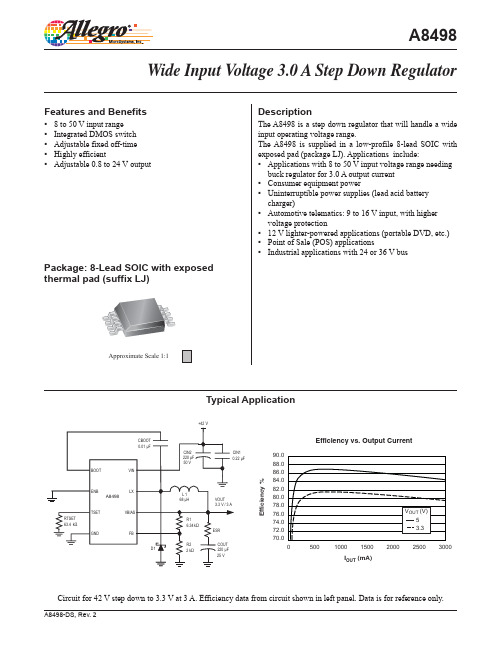
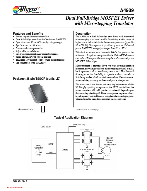
Description
The A8498 is a step down regulator that will handle a wide input operating voltage range. The A8498 is supplied in a low-profile 8-lead SOIC with exposed pad (package LJ). Applications include: ▪ Applications with 8 to 50 V input voltage range needing
Wide Input Voltage 3.0 A Step Down Regulator
Functional Description
The A8498 is a fixed off-time, current-mode–controlled buck switching regulator. The regulator requires an external clamping diode, inductor, and filter capacitor, and operates in both continuous and discontinuous modes. An internal blanking circuit is used to filter out transients resulting from the reverse recovery of the external clamp diode. Typical blanking time is 200 ns.
FTLF8524P2BNV中文资料
II.
Absolute Maximum Ratings
Symbol Vcc TS TA RH Min -0.5 -40 -20 0 Typ Max 4.0 85 85 85 Unit V °C °C % Ref.
Parameter Maximum Supply Voltage Storage Temperature Case Operating Temperature Relative Humial Characteristics (TA = -20 to 85 °C, VCC = 3.0 to 3.6 Volts)
Pin Descriptions
Symbol VEET TFAULT TDIS MOD_DEF(2) MOD_DEF(1) MOD_DEF(0) Rate Select LOS VEER VEER VEER RDRD+ VEER VCCR VCCT VEET TD+ TDVEET Name/Description Transmitter Ground (Common with Receiver Ground) Transmitter Fault. Not supported. Transmitter Disable. Laser output disabled on high or open. Module Definition 2. Data line for Serial ID. Module Definition 1. Clock line for Serial ID. Module Definition 0. Grounded within the module. 1.063 Gb/s or 2.125 Gb/s Fibre Channel, 1.25 Gb/s Open or Low = Gigabit Ethernet (Low Bandwidth) 2.125 or 4.25 Gb/s Fibre Channel (High Bandwidth) High = Loss of Signal indication. Logic 0 indicates normal operation. Receiver Ground (Common with Transmitter Ground) Receiver Ground (Common with Transmitter Ground) Receiver Ground (Common with Transmitter Ground) Receiver Inverted DATA out. AC Coupled Receiver Non-inverted DATA out. AC Coupled Receiver Ground (Common with Transmitter Ground) Receiver Power Supply Transmitter Power Supply Transmitter Ground (Common with Receiver Ground) Transmitter Non-Inverted DATA in. AC Coupled. Transmitter Inverted DATA in. AC Coupled. Transmitter Ground (Common with Receiver Ground) Ref. 1 2 3 3 3 4 5 1 1 1
AO4924中文资料
AO4924Asymmetric Dual N-Channel Enhancement Mode Field Effect TransistorAO4924SymbolMin TypMaxUnits BV DSS 30V V DS =24V, V GS =0V0.010.1T J =125°C510I GSS 0.1µA V GS(th)Gate Threshold Voltage 1.5 1.852.4V I D(ON)40A 1315.8T J =125°C20.025.015.719.5m Ωg FS 64S V SD 0.40.6V I S4.5A C iss 14501885pF C oss 224pF C rss92pF R g 1.6 3 ΩQ g (10V)24.031Q g (4.5V)12.0nC Q gs 3.9nC Q gd 4.2nC t D(on) 5.5ns t r 4.7ns t D(off)24.0ns t f 4.0ns t rr 1013ns Q rr6.8nCTHIS PRODUCT HAS BEEN DESIGNED AND QUALIFIED FOR THE CONSUMER MARKET. APPLICATIONS OR USES AS CRITICAL COMPONENTS IN LIFE SUPPORT DEVICES OR SYSTEMS ARE NOT AUTHORIZED. AOS DOES NOT ASSUME ANY LIABILITY ARISING OUT OF SUCH APPLICATIONS OR USES OF ITS PRODUCTS. AOS RESERVES THE RIGHT TO IMPROVE PRODUCT DESIGN,FUNCTIONS AND RELIABILITY WITHOUT NOTICE.Body Diode Reverse Recovery Time Body Diode Reverse Recovery ChargeI F =9A, dI/dt=300A/µsDrain-Source Breakdown Voltage On state drain currentI D =1mA, V GS =0V V GS =4.5V, V DS =5V V GS =10V, I D =9AReverse Transfer CapacitanceI F =9A, dI/dt=300A/µs V DS =V GS I D =250µA FET1 Electrical Characteristics (T J =25°C unless otherwise noted)STATIC PARAMETERS Parameter Conditions I DSS Zero Gate Voltage Drain Current mA V DS =0V, V GS = ±12V Gate-Body leakage current R DS(ON)Static Drain-Source On-ResistanceForward TransconductanceDiode Forward VoltageMaximum Body-Diode + Schottky Continuous CurrentInput Capacitance Output Capacitance DYNAMIC PARAMETERS m ΩV GS =4.5V, I D =7AI S =1A,V GS =0V V DS =5V, I D =9ATurn-On Rise Time Turn-Off DelayTime V GS =10V, V DS =15V, R L =1.7Ω, R GEN =3ΩTurn-Off Fall TimeTurn-On DelayTime Total Gate Charge V GS =10V, V DS =15V, I D =9AGate Drain Charge V GS =0V, V DS =15V, f=1MHzSWITCHING PARAMETERS Total Gate Charge Gate Source Charge Gate resistance V GS =0V, V DS =0V, f=1MHz A: The value of R θJA is measured with the device in a still air environment with T A =25°C. The power dissipation P DSM and current rating I DSM are based on T (J(MAX)=150°C, using t ≤ 10s junction-to-ambient thermal resistance.B: Repetitive rating, pulse width limited by junction temperature T J(MAX)=150°C.C. The R θJA is the sum of the thermal impedence from junction to lead R θJL and lead to ambient.D. The static characteristics in Figures 1 to 6 are obtained using <300 µs pulses, duty cycle 0.5% max.E. These tests are performed with the device mounted on 1 in 2 FR-4 board with 2oz. Copper, in a still air environment with T A =25°C. The SOA curve provides a single pulse rating. Rev0:Sept. 2006AO4924AO4924AO4924AO4924SymbolMin TypMaxUnits BV DSS 30V 1T J =55°C5I GSS 100nA V GS(th)0.711.5V I D(ON)40A 2024T J =125°C283423.529m Ωg FS 26S V SD 0.711V I S4.5A C iss 9001100pF C oss 88pF C rss 65pF R g0.95 1.5ΩQ g 1012nC Q gs 1.8nC Q gd 3.75nC t D(on) 3.2ns t r 3.5ns t D(off)21.5ns t f 2.7ns t rr 16.820ns Q rr812nCTHIS PRODUCT HAS BEEN DESIGNED AND QUALIFIED FOR THE CONSUMER MARKET. APPLICATIONS OR USES AS CRITICAL COMPONENTS IN LIFE SUPPORT DEVICES OR SYSTEMS ARE NOT AUTHORIZED. AOS DOES NOT ASSUME ANY LIABILITY ARISING OUT OF SUCH APPLICATIONS OR USES OF ITS PRODUCTS. AOS RESERVES THE RIGHT TO IMPROVE PRODUCT DESIGN,FUNCTIONS AND RELIABILITY WITHOUT NOTICE.Body Diode Reverse Recovery TimeBody Diode Reverse Recovery Charge I F =7.3A, dI/dt=100A/µsDrain-Source Breakdown Voltage On state drain currentI D =250µA, V GS =0V V GS =4.5V, V DS =5V V GS =10V, I D =7.3AReverse Transfer Capacitance FET2 Electrical Characteristics (T J =25°C unless otherwise noted)STATIC PARAMETERS ParameterConditions I DSS µA Gate Threshold Voltage V DS =V GS I D =250µA V DS =24V, V GS =0VV DS =0V, V GS = ±12V Zero Gate Voltage Drain Current Gate-Body leakage current R DS(ON)Static Drain-Source On-ResistanceForward TransconductanceDiode Forward Voltage I F =7.3A, dI/dt=100A/µsV GS =0V, V DS =15V, f=1MHz SWITCHING PARAMETERS Total Gate Charge V GS =4.5V, V DS =15V, I D =7.3AGate Source Charge Gate Drain Charge Turn-On Rise Time Turn-Off DelayTime V GS =10V, V DS =15V, R L =2Ω, R GEN =6ΩTurn-Off Fall TimeMaximum Body-Diode Continuous CurrentInput Capacitance Output Capacitance Turn-On DelayTime DYNAMIC PARAMETERS Gate resistanceV GS =0V, V DS =0V, f=1MHzm ΩV GS =4.5V, I D =6AI S =1A,V GS =0V V DS =5V, I D =7.3AA: The value of R θJA is measured with the device mounted on 1in 2FR-4 board with 2oz. Copper, in a still air environment with T A =25°C. The value in any given application depends on the user's specific board design. The current rating is based on the t ≤ 10s thermal resistance rating.B: Repetitive rating, pulse width limited by junction temperature.C. The R θJA is the sum of the thermal impedence from junction to lead R θJL and lead to ambient.D. The static characteristics in Figures 1 to 6 are obtained using <300 µs pulses, duty cycle 0.5% max.E. These tests are performed with the device mounted on 1 in 2FR-4 board with 2oz. Copper, in a still air environment with T A =25°C. The SOA curve provides a single pulse rating. Rev 0 : Sept. 2006AO4924AO4924。
SGM8521中文资料
SGM8521 SGM8522 SGM8524PRODUCT DESCRIPTIONThe SGM8521 (single),SGM8522 (dual) and SGM8524 (quad) are rail-to-rail input and output voltage feedback amplifiers offering low cost. They have a wide input common-mode voltage range and output voltage swing, and take the minimum operating supply voltage down to 2.1V and the maximum recommended supply voltage is 5.5 V. All are specified over the extended –40°C to +125°C temperature range.The SGM8521/8522/8524 provide150KHz bandwidth at a low current consumption of 4.7µA per amplifier. Very low input bias currents of 0.5pA, enable the SGM8521/8522/8524 to be used for integrators, photodiode amplifiers, and piezoelectric sensors. Rail-to-Rail inputs and outputs are useful to designers buffering ASIC in single-supply systems.Applications for these amplifiers include safety monitor- ing, portable equipment, battery and power supply control, and signal conditioning and interfacing for transducers in very low power systems.The SGM8521 is available in the tiny SOT23-5 and SO-8 packages. The SGM8522 comes in the miniature SO-8 and MSOP-8 packages. The SGM8524 is offered in TSSOP-16 SO-16 and SO-14 packages.APPLICATIONSASIC Input or Output Amplifier Sensor InterfacePiezo Electric Transducer Amplifier Medical Instrumentation Mobile Communication Audio Output Portable Systems Smoke Detectors Mobile Telephone Notebook PC PCMCIA cardsBattery-Powered equipment150KHz, 4.7µA, Rail-to-Rail I/O CMOS Operational AmplifierFEATURES• Low Cost• Rail-to-Rail Input and Output0.8mV Typical V OS • Unity Gain Stable• Gain Bandwidth Product: 150KHz • Very low input bias currents : 0.5pA • Operates on 2.1 V to 5.5 V Supplies• Input Voltage Range = - 0.1 V to +5.6 V with V S = 5.5V • Low Supply Current: 4.7µA/Amplifier • Small PackagingSGM8521 Available in SO-8 and SOT23-5 SGM8522 Available in SO-8 and MSOP-8 SGM8524 Available in SO-16, SO-14 and TSSOP-16PIN CONFIGURATIONS (Top View)S NC-IN +IN -V SNC NC OUT +V S-V SOT23-5OUT B S -V SO-8 / MSOP-8OUT S +V -IND+IND SO-16/TSSOP-16-INB +INB -INC NCNCOUT BOUT C +INC OUT D OUT -V S +V -IND+IND-INC OUT BOUT C+INC OUT DShengbang Microelectronics Co, LtdPreliminary DatasheetREV . BELECTRICAL CHARACTERISTICS : V S = +5V (At R L = 500kΩ connected to Vs/2 and V OUT = Vs/2, unless otherwise noted)Specifications subject to change without notice.PACKAGE/ORDERING INFORMATIONMODEL ORDER NUMBER PACKAGEDESCRIPTIONPACKAGE OPTION MARKING INFORMATIONSGM8521XN5/TRSOT23-5Tape and Reel, 30008521 SGM8521SGM8521XS/TR SO-8 Tape and Reel, 2500 SGM8521XS SGM8522XS/TR SO-8 Tape and Reel, 2500 SGM8522XS SGM8522SGM8522XMS/TRMSOP-8Tape and Reel, 3000SGM8522XMS SGM8524XS/TR SO-16 Tape and Reel, 2500SGM8524XSSGM8524XS14 SO-14Tube SGM8524XS14SGM8524SGM8524XTS/TR TSSOP-16 Tape and Reel, 3000SGM8524XTSABSOLUTE MAXIMUM RATINGSSupply Voltage, V+ to V- . . . . . . . . . . . . . . . . . . . . . 7.5 VCommon-Mode Input Voltage. . . . . . . . . . . . . . . . . . . . (–V S ) – 0.5 V to (+V S )+0.5V Storage Temperature Range . . . . . . . . .–65℃ to +150℃ Junction Temperature . . . . . . . . . . . . . . . .. . . . . . . .160℃ Operating Temperature Range . . . . . . –55℃ to +150℃Package Thermal Resistance @ T A = 25℃SOT23-5, θJA .............................................................. 190/℃W SO-8, θJA ......................................................................125/W ℃ MSOP-8, θJA .............................................................. 216/W ℃ SO-16, θJA ..................................................................... 82/W ℃ TSSOP-16, θJA ............................................................ 105/W ℃ Lead Temperature Range (Soldering 10 sec).....................................................260℃ESD SusceptibilityHBM................................................................................4000V MM (400V)NOTES1. Stresses above those listed under Absolute Maximum Ratings may cause permanent damage to the device. This is a stress rating only; functional operation of the device at these or any other conditions above those indicated in the operational section of this specification is not implied. Exposure to absolute maximum rating conditions for extended periods may affect device reliability.CAUTIONThis integrated circuit can be damaged by ESD. Shengbang Micro-electronics recommends that all integrated circuits be handled with appropriate precautions. Failure to observe proper handling and installation procedures can cause damage.ESD damage can range from subtle performance degradation to complete device failure. Precision integrated circuits may be more susceptible to damage because very small parametric changes could cause the device not to meet its published specifications.TYPICAL PERFORMANCE CHARACTERISTICSAt T A = +25℃, V S = +5V , and R L =500k Ω connected to Vs/2,unless otherwise noted.Small-Signal Step Response Small-Signal Step Response50µs/div 50µs/divG = +1R L= 500K ΩC L = 20pFG = +1 R L= 500K ΩC L = 100pFG = +1 C L = 100pF R L= 500K Ω50m V /d i v50m V /d i v1V /d i vLarge-Signal Step Response100µs/divTYPICAL PERFORMANCE CHARACTERISTICS At T A= +25℃, V S = +5V, and R L=500kΩ connected to Vs/2,unless otherwise noted.APPLICATION NOTESDriving Capacitive LoadsThe SGM852X can directly drive 250pF in unity-gain without oscillation. The unity-gain follower (buffer) is the most sensitive configuration to capacitive loading. Direct capacitive loading reduces the phase margin of amplifiers and this results in ringing or even oscillation. Applications that require greater capacitive drive capability should use an isolation resistor between the output and the capacitive load like the circuit in Figure 1. The isolation resistor R ISO and the load capacitor C L form a zero to increase stability. The bigger the R ISO resistor value, the more stable V OUT will be. Note that this method results in a loss of gain accuracy because R ISO forms a voltage divider with the R LOAD.V IN V OUTFigure 1. Indirectly Driving Heavy Capacitive LoadAn improvement circuit is shown in Figure 2, It provides DC accuracy as well as AC stability. R F provides the DC accuracy by connecting the inverting signal with the output, C F and R Iso serve to counteract the loss of phase margin by feeding the high frequency component of the output signal back to the amplifier’s inverting input, thereby preserving phase margin in the overall feedback loop.V IN V OUTFigure 2. Indirectly Driving Heavy Capacitive Load with DC AccuracyFor no-buffer configuration, there are two others ways to increase the phase margin: (a) by increasing the amplifier’s gain or (b) by placing a capacitor in parallel with the feedback resistor to counteract the parasitic capacitance associated with inverting node. Power-Supply Bypassing and Layout The SGM852X family operates from either a single +2.5V to +5.5V supply or dual ±1.25V to ±2.75V supplies. For single-supply operation, bypass the power supply V DD with a 0.1µF ceramic capacitor which should be placed close to the V DD pin. For dual-supply operation, both the V DD and the V SS supplies should be bypassed to ground with separate 0.1µF ceramic capacitors. 2.2µF tantalum capacitor can be added for better performance.VnVpV SSV SS(GND)Figure 3. Amplifier with Bypass CapacitorsTypical Application Circuits Differential AmplifierThe circuit shown in Figure 4 performs the difference function. If the resistors ratios are equal ( R4 / R3 = R2 / R1 ), thenV OUT = ( Vp – Vn ) × R2 / R1 + Vref.Vn VpOUT Figure 4. Differential AmplifierInstrumentation AmplifierThe circuit in Figure 5 performs the same function as that in Figure 4 but with the high input impedance.Vn VpV OUT Figure 5. Instrumentation AmplifierLow Pass Active FilterThe low pass filter shown in Figure 6 has a DC gain of ( - R2 / R1 ) and the –3dB corner frequency is 1/2πR2C. Make sure the filter is within the bandwidth of the amplifier. The Large values of feedback resistors can couple with parasitic capacitance and cause undesired effects such as ringing or oscillation in high-speed amplifiers. Keep resistors value as low as possible and consistent with output loading consideration.V INV OUT Figure 6. Low Pass Active FilterPACKAGE OUTLINE DIMENSIONS SOT23-5PACKAGE OUTLINE DIMENSIONS SO-8PACKAGE OUTLINE DIMENSIONS MSOP-8PACKAGE OUTLINE DIMENSIONS SO-16PACKAGE OUTLINE DIMENSIONS TSSOP-16PACKAGE OUTLINE DIMENSIONS SO-14REVISION HISTORYLocation Page 11/06— Data Sheet changed from Preliminary to REV. AChanges to ABSOLUTE MAXIMUM ATINGS . . . . . . . . . . . . . . . . . . . . . . . . . . . . . . . .. . . . . . . . . . . . . . . . . . . . . . . . . . .. . . . . . . 3 11/06— Data Sheet changed from REV. A to REV. BAdds SO-14 Package . . . . . . . . . . . . . . . . . . . . . . . . . . . . . . . .. . . . . . . . . . . . . . . . . . . . . . . . . . . .. . . . . . . . . . . . . . . .. . . . . . 1, 3Shengbang Microelectronics Co, LtdUnit 3, ChuangYe PlazaNo.5, TaiHu Northern Street, YingBin Road Centralized Industrial ParkHarbin Development ZoneHarbin, HeiLongJiang 150078P.R. ChinaTel.: 86-451-84348461Fax: 86-451-84308461。
SC8521资料
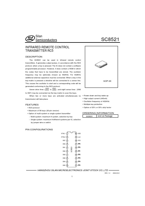
SilanSemiconductors SC8521HANGZHOU SILAN MICROELECTRONICS JOINT-STOCK CO.,LTDREV:1.32002.03.011INFRARED REMOTE CONTROLTRANSMITTER RC5DESCRIPTIONThe SC8521can be used in infrared remote controltransmitters.It generates output pulses,in accordance with the RC5protocol,when a key is pressed.The IC does not contain a softwareprogrammable processor.However,it does contain a ROM in whichthe codes that have to be transmitted are stored.The oscillatorfrequency may be optionally chosen as432KHz.For432KHzadditional external capacitors must be connected.When a key in thekey-matrix is pressed a driveline will be connected to a sense line.This causes the oscillator to start and a corresponding code will begenerated conforming to the RC5protocol.Seven drive lines(DR0to DR6)and eight sense lines(SN0to SN7)may be connected via the key matrix to scan the keys.When two or more keys are activated simultaneously notransmission will take place.FEATURES∗ RC5protocol∗ Maximum of56keys(20-pin version)∗ Option of multi-system or single system transmitter--Multi-system:maximum8system,selection by key--Single system:maximum8different systems per IC,selectionby jumper wire or switch.∗ Power-down and key wake-up∗ High output current(≤45mA)∗ Oscillator frequency of432KHz∗ Multiple key protection∗ Option of25%or33%duty factorORDERING INFORMATIONSC8521SOP-20PackagePIN CONFIGURATIONSXTAL1XTAL2SN0SN1SN2SN3SN4SN5VDDLoutVSSDR0DR2DR3SN6SN7DR6DR5SilanSemiconductors SC8521HANGZHOU SILAN MICROELECTRONICS JOINT-STOCK CO.,LTDREV:1.32002.03.012BLOCK DIAGRAMSN0SN1SN2SN3SN4SN5SN6SN7DR0DR1DR2DR3DR4DR5DR6Lout432kHZABSOLUTE MAXIMUM RATINGCharacteristic Symbol Value Unit Supply Voltage V DD5VPower Dissipation P D25mWThermal Derating K∂10mW/°CStorage Temperature T STG-65~+150°COperating Temperature T OPR-20~+80°CSilanSemiconductors SC8521HANGZHOU SILAN MICROELECTRONICS JOINT-STOCK CO.,LTDREV:1.32002.03.013ELECTRICAL CHARACTERISTICS (Tamb=25°C,unless otherwise specified)Symbol ParameterTestconditionMinTypeMaxUnit Operating supply voltage V DD 2.2-- 4.5VSupply current I DD V DD=3V;TA=25°C----2mAQuiescent current I DD(q)V DD=3V;TA=25°C----1µAOperating ambient temperature T A-10--+50°CSense lines(input only and will have a weak internal pull-up resistance)LOW level input voltage V IL----0.3V DD VHIGH level input voltage V IH0.7V DD----VPull-up resistance Rpu V DD=3V50--100KΩDriver lines(output only;open drain;maximum on-resistance when LOW)Maximum on-resistance Ron V DD=3V----2KΩOutput drive(has a weak pull-up resistance)Source current Isink V DD=3V;VO=1.5V 3.5 4.5 5.5mAPIN DESCRIPTION20-pin dual in-line and small outline package(SO-20)To be continuedSilanSemiconductors SC8521HANGZHOU SILAN MICROELECTRONICS JOINT-STOCK CO.,LTDREV:1.32002.03.014FUNCTION DESCRIPTION1. Key numbering for matrix is given in tables 1Table1key numbering for20-pin packageSN0connected GND,send BANK7code.BANK0----7see the following code table.When the keys have been scanned the key-number of the activated key serves as the address of the ROM to obtain the required codeword.Consequently,key numbers6,7,14,15,22,23,30,31,38,39and40to55will not be addressed.The ROM contains8banks of64code words.Thus for each key a maximum of8different code words may be generated.With multi-system use,8different systems(,VCR,tuner,CD etc.)may be selected.Apart from the system bits the command bits may also be different in different banks(true multi-function keys).Selection can be performed using the keys.For each key three bank selected bits are present that determine which bank will be selected for the next key.For each key an‘inhibit’bit is also present.When this bit is at logic1at an address in a given bank,and when the corresponding key is pressed(when this bank has been selected)no transmission will take place.A single system option is available however,whereby instead of keys jumper wire and/or a switch may be used for bank ing this option it is possible to program different transmitter models in one IC and select the required bank by means of jumper wire.Instead of a jumper wire a side-switch may also be used to change theSilanSemiconductors SC8521HANGZHOU SILAN MICROELECTRONICS JOINT-STOCK CO.,LTDREV:1.32002.03.015generated code temporarily(select different bank)to obtain multi-function keys.With this option the jumper wires or switch must be connected between sense line SN0and one of the drivelines DR0to DR6or ground.This means that SN0cannot be used to connect keys and the maximum number of keys will be49keys for a20-pin package.It is not possible to use a combination of jumper wires and selection keys for bank selection in one unit.The output of the ROM is loaded into a shift register that provides the input bits for the pulse generator.This pulse generator drives the output pin.2. Timing generatorA schematic diagram of the timing generator is illustrated the oscillator frequency is432KHz.The timing generator is stopped when no key is activated and started again when a key is pressed.The output of the oscillator(CLK1)is divided by12for432KHz.Selection is achieved using a mask option.The output of the divider is CLK2which is used for clocking of the control timer.The frequency of CLK2is36KHz and the inverse is used to generate the output pulses in the subcarrier frequency.By mask option the duty factor can be chosen to be25%or33%.The control timer has a length of4096subcarrier(pulse)periods.This is equal to the transmission repletion time.A bit time is equal to64pulses and the repetition time is64bit times.The control timer provides the timing of the key scanning,the ROM access and the code transmission.When the control timer has arrived at a certain state and no key has been pressed for at least28ms,a stop signal will be generated which will stop the oscillator.All drivelines will then be set to logic0.As soon as a key is pressed one of the sense lines will become logic0.This will generate a start signal,which will restart the oscillator.no keyend controlstart inputTimer schematic diagramSilanSemiconductors SC8521HANGZHOU SILAN MICROELECTRONICS JOINT-STOCK CO.,LTDREV:1.32002.03.0163. Single systemSN0should be connected to one of the drivelines or ground.The bank that will be selected is equal to drive line number to which SN0is connected.When connected toground the number will be7.This achieved by loading the bank select flip-flops BS0to BS2with the contents ofC5to C7of the control timer when sense line SN0is at logic0.In this way it is possible to use two different systems in one transmitter by using a side switch.With this option SN0cannot be used to connect keys,so the maximum number of keys will be lower(49keys with20-pin IC).4. Multi systemThe bank is selected by key for maximum8different systems(,VCR,CD,etc.),any key is flexible forbank selection.When a user inserts a new battery,the default bank is always in bank7.If only bank7is used,then maximum number of key can be56keys for a20-pin IC5. ROMLogic 1Logic 0A schematic diagram of the ROM is illustrated.The ROM is divided into8banks of2×64bytes.Bank selectionis performed using flip-flops BS0to BS2that are the3highest bits of the address.With the‘single system’thesebits are loaded from the3MSBs of the scan control when SN0=0.At power-on the bank select flip-flops will be inan arbitrary state.When a key was activated,the key number is stored in the6-bit key register.This register forms the lower bits ofthe ROM address.For each command the ROM will be accessed twice.This gives16bits in total(M0L to M7Land M0H to M7H).The bits are described in Table2.Table2ROM bit descriptionBits Function M0L to M5L Command bits0to5M6LField bit.This bit indicates whether command codes0to63are used(filed bit is at logic1)or command codes64to127are used(filed bit is at logic0).M7LInhibit bit.When this bit is at logic1no transmission will take place.When this bit is atlogic0the appropriate code word will be transmitted.M0H to M4H System bits0to4M5H to M7HBank select.Will be stored in BS0to BS2when the‘multi-system’option is selected.Withsingle system bits M5H to M7H are don’t care.SilanSemiconductors SC8521HANGZHOU SILAN MICROELECTRONICS JOINT-STOCK CO.,LTDREV:1.32002.03.0176. Pulse outputThe bits of the remote control word,as indicated by the addressed ROM locations,are loaded into a shift register every bit-time this register is shifted.The output is used to generate a logic1in the biphase(Manchester) coding,modulated with a frequency of36KHz.The duty factor of the modulation pulses may be selected (optionally)to be25%or33.3%.The output of the pulse generator controls the output driver that can provide a maximum current of5mA.DR5DR4DR3DR2DR1DR0DR6SN0SN7SN1SN2SN3SN6SN4SN5Scan timing.SilanSemiconductors SC8521HANGZHOU SILAN MICROELECTRONICS JOINT-STOCK CO.,LTDREV:1.32002.03.018ROM1Kx8ROM schematic diagramSYSTEM DEVELOPMENT1. Software (SC8521)A PC program is provided that enables the user to fill in system and command codes for each keys number in each bank.This program converts the input data into a ROM code-file needed to produce the metal mask and to program an EPROM to be used in the hardware emulator.2. HardwareAn emulator is available that functionally emulates the IC.An EPROM with the ROM code information is inserted into the emulator to produce the required remote control codes corresponding to the keys in the prototype device.SilanSemiconductors SC8521HANGZHOU SILAN MICROELECTRONICS JOINT-STOCK CO.,LTDREV:1.32002.03.019INTERNAL PIN CONFIGURATION1.Pin configuration for pin SN02.Pin configuration for pins SN1toSN743,5to103.Pin configuration for pins DR0to DR64.Pin configuration for pinLoutto1719 APPLICATION CIRCUITApplication diagram(SO20package)SilanSemiconductors SC8521HANGZHOU SILAN MICROELECTRONICS JOINT-STOCK CO.,LTDREV:1.32002.03.0110INSTRUCTION AND SIGNAL OUTPUT FORMAT (Binary)KeyBank0 Bank1 Bank2 Bank3 k0////k110000111010011110001001011101100101110010011010100101011k210000111010010110001000111011100101101001111010100011101k311000111101100110001000111111100101101001011010100110010k411000000001100100001001000001100101100110011010100111111k511000111010001100001001011001100101110010110010100101100k611000111011110110001001011011100101100111111010100101101k711000111010000110001000111001100101100110111010100011100k8////k910000111001110110001000000111100101100001111010100000011k1010000111001101110001001000011000101101101111010100100001k1110000000100001110001001000001000101101100111010100100000k1211000111111010100001000011111100101110000011010101111111k1311000111010111110001000010011100101100100111010100001001k1411000000100100110001001101011100101110000111010100110101k1511000111010110110001000001101100101100011011010100000110k16////k1710000111000100100001001101001100101101101011010000001101k1811000111011101110001000010101100101110100111010100001011k19/100001001100011000101111111010010000001111k2010000111000101100001000011001100101101011011010001101011k2111000111110110100001001101111100101101011111010001011111k2211000111010101100001000001011100101111111011010001101110k2311000111110101100001001101101100101101000011010000010000k24////k2510000000111010110001000000101100101100001011010100000010k2610000000010001100001001100111000101101000110010100110011k2710000000010010100001001100101000101101000010010100110010(To be continued)SilanSemiconductors SC8521HANGZHOU SILAN MICROELECTRONICS JOINT-STOCK CO.,LTDREV:1.32002.03.0111ContinuedKeyBank0 Bank1 Bank2 Bank3 k2811000000001101100001000110001100101110001011010010111111k2911000111011001110001000010001100101100100011010100001000k3010000000010000110001001100001100101110001111010100110000k3111000111011000110001000001011100101100010111010100000101k32////k3311000111011101110001000000011100101100000111000100000001k3411000111011100110001001110111000101101101011010100111011k3510000000010101110001001010101000101101100011010100110100k3611000000100011110001001010001000101111111111010001111111k3711000111011011110001000001111100101100011111010100000111k3810000111111111110001001101101100101110110111010100110110k3911000111011010110001000001001100101100010011010100000100k40////k411100011100000011000100010001/10010000000000k42/11000100010000/10010000000110k4311000111011100110001001001001000101101110111010100100100k4411000111010100110001000000001100101100000011010100000000k45/10000100110000/11010000001111k4611000111100111100001000001101000101101110011010100001111k47/11000100001100/k48////k4910000111000011110001001010111100101101101111010000100110k5011000111010011110001000011111100101110111011010001001100k5111000111010010100001001010111100101110101110010100101011k5210000111000110100001000010111100101101100011010001100001k5311000111110111100001000000111100101101100111010001011110k541100011101111110000100000100110010111111111101000110000k5511000111110100100001001011111100101101000111010000010001SilanSemiconductors SC8521HANGZHOU SILAN MICROELECTRONICS JOINT-STOCK CO.,LTDREV:1.32002.03.0112KeyBank4 Bank5 Bank6 Bank7 k0////k111010100011101100000001011011000000010110111000000110010k211010001011111100000001011001000000010110011000000110110k311010001011110100000001010111000000010101111000000110111k411010100001100110000000011001100000000110011000000001100k511010100011100100000001011111000000010111111000000110101k610010100101011100000001111101000000011111010000000111110k711010100101011100000001011101000000010111011000000110100k8////k911010100000011110000000000111100000000001111000000000011k1011010100100001110000001001101000000010000111000000100110k1111010100100000100000000101101000000001011011000000010000k1211010100101101110000000011101100000000111011000000001110k1311010100001001110000000010011100000000100111000000001001k1411010100110101110000001001001100000010010011000000100100k1511010100000110110000000001101100000000011011000000000110k16////k1711010000011010110000001011001100000010110011000000101100k1811010001111111110000000100001000000001100110000000011001k1911010100111011/10000000100101/k2011010000010110110000001010111100000010101111000000101011k2111010000010111110000001010101100000010101011000000101010k2211010010111111110000001000011000000010011111000000001011k2311010000010000110000001010111100000010101111000000101101k24////k2511010100000010110000000000101100000000001011000000000010k2611010100110010100000000100011000000001000111000000100001k2711010100110100100000000100101000000001001011000000111011k2811010100001011110000000011011100000000110111000000001101(To be continued)SilanSemiconductors SC8521HANGZHOU SILAN MICROELECTRONICS JOINT-STOCK CO.,LTDREV:1.32002.03.0113(Continued)KeyBank4 Bank5 Bank6 Bank7 k2911010100001000110000000010001100000000100011000000001000k3011010100110110100000000100001000000001000011000000100000k3111010100000101110000000001011100000000010111000000000101k32////k3311000100000001110000000000011100000000000111000000000001k3411010001100001100000001101011000000011010110000000110101k3511010001100000100000000101011000000001010111000000010001k3611010000100110110000001000111100000010001111000000100011k3711010100000111110000000001111100000000011111000000000111k3810010100101100110000000011111100000000111111000000001111k3911010100000100110000000001001100000000010011000000000100k40////k41/110001110000001000000001101011000111000000k42//10000000011111/k4310010100110011110000001110001100000011100011000000111000k4411010100000000110000000000001100000000000011000000000000k45110101001100001000000011000110000000110001/k4610010100110010110000001000101100000010001011000000100010k47 110001111110101100011111101011000111111010k48////k4911010000011011110000001111001100000011110011000000111100k5011010100111111110000000100011000000001100010000000011000k5111010100100100110000001111111100000011111111000000111111k5211010000011000110000001010011100000010100111000000101001k5311010000011001100000001110101000000011101011000000011110k5411010101111111110000001000001000000010011011000000001010k55110100000100011100000010111011000000101110110000001011101 The number after K is the key code number.2 The number after B is BANK0,BANK1number.When SN0connect the GND,it sends BANK7.3 Don’t compatible with PCA8521pins.SilanSemiconductors SC8521HANGZHOU SILAN MICROELECTRONICS JOINT-STOCK CO.,LTDREV:1.32002.03.0114PCB WIRE LAYOUT SCHEMATIC:layout separated or overstriking ground line.The above IC only use to hint,not to specified.Note:*In wire layout,the power filter capacitor should near to IC.*In wire layout,should avoid power line and ground line too long.*Recommended infrared transmit unit and IC ground line should layout separated,or overstriking lines.*The emitter of triode connect1¡resistor at least.*Recommended triode use9014.SilanSemiconductors SC8521HANGZHOU SILAN MICROELECTRONICS JOINT-STOCK CO.,LTDREV:1.32002.03.0115SilanSemiconductors SC8521HANGZHOU SILAN MICROELECTRONICS JOINT-STOCK CO.,LTDREV:1.32002.03.0116AttachRevision HistoryData REV Description Page 2001.09.18 1.0Original2001.01.03 1.1Modify the order of the pin in key matrix table4 2002.01.19 1.2Modify the diode direction in“APPLICATION CIRCUIT”Add the Binary“instruction and signal output format table”Add the note of instruction table.910~1313~14 2002.03.01 1.3The102pF capacitor change to100pF in“APPLICATION CIRCUIT”Add the“PCB wire layout schematic”Modify the“Package outline”91415。
HS91-98704中文资料
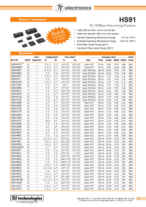
Specifications
BI P/N1 RoHS2 LF LF LF LF LF LF LF LF
3 3
Ports Supported 1 1 1 1 1 1 1 1 1 1 1 1 1 1 1 1 1 1 1 1 1 1 1 1 1 1 1 1 1 1 1 1 1 1 1 1 1 1 1 1 1 1 1
Packaging (mm) Hi-Pot Pitch Length Width Height Vrms) 79 mil 79 mil 100 mil 100 mil 50 mil 50 mil 50 mil 50 mil 50 mil 50 mil 50 mil 50 mil 50 mil 50 mil 50 mil 50 mil 50 mil 50 mil 50 mil 50 mil 50 mil 50 mil 50 mil 50 mil 50 mil 100 mil 100 mil 100 mil 100 mil 100 mil 100 mil 100 mil 100 mil 100 mil 100 mil 100 mil 100 mil 100 mil 100 mil 100 mil 100 mil 100 mil 100 mil 14.81 14.81 20.32 20.32 11.81 11.81 11.81 11.81 14.22 14.22 12.70 12.70 12.70 12.70 12.70 12.70 12.70 12.70 12.70 12.70 12.70 12.70 12.70 12.70 12.70 25.40 25.40 25.40 25.40 25.40 25.40 25.40 25.40 25.40 25.40 25.40 25.40 25.40 25.40 25.40 25.40 25.40 25.40 14.73 15.20 17.40 17.40 11.43 11.43 11.43 11.43 17.01 17.01 9.30 9.60 9.52 9.65 9.65 9.65 9.35 9.26 9.35 9.53 9.65 9.35 9.65 9.65 9.65 12.70 12.70 12.70 12.70 12.70 12.70 12.70 12.70 12.70 12.70 12.70 12.70 12.70 12.70 12.70 12.70 12.70 12.70 4.88 4.88 2.49 2.39 2.16 2.19 2.16 2.16 2.20 2.20 1.95 2.08 1.98 6.22 6.22 6.22 6.22 6.06 5.08 5.73 5.98 6.22 5.98 6.22 5.98 7.00 7.00 7.00 7.00 5.97 7.00 7.00 7.00 7.00 7.00 7.00 7.00 7.00 7.00 7.00 7.00 6.05 7.00 1500 1500 1500 1500 1500 1500 1500 1500 1500 1500 1500 1500 1500 1500 1500 1500 1500 1500 1500 1500 1500 1500 1500 1500 1500 1500 1500 1500 1500 1500 1500 1500 1500 1500 1500 1500 1500 1500 1500 1500 1500 1500 1500
S852T中文资料
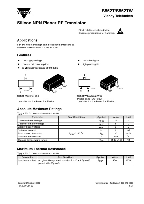
S852T/S852TW
Vishay Telefunken
Silicon NPN Planar RF Transistor
Electrostatic sensitive device. Observe precautions for handling.
Applications
0.5 0.4 0.3 0.2 0.1 0 0 1 2 3 4 5 VCB – Collector Base Voltage ( V )
13622
Figure 1. Total Power Dissipation vs. Ambient Temperature
7000 f T – Transition Frequency ( MHz ) f=500MHz 6000 5000 4000 3000 2000 1000 0 0
0.1 90
Electrical AC Characteristics
Tamb = 25_C, unless otherwise specified Parameter Transition frequency q y Collector-base capacitance Noise figure Test Conditions VCE = 3 V, IC = 1 mA, f = 500 MHz VCE = 2 V, IC = 1.5 mA, f = 500 MHz VCB = 1 V, f = 1 MHz ZS = ZSopt, f = 450 MHz, VCE = 2 V, IC = 0.5 mA ZS = ZSopt, f = 945 MHz, VCE = 3 V, IC = 1 mA ZS = ZSopt, f = 945 MHz, VCE = 2 V, IC = 1.5 mA VCE = 2 V, IC = 0.5 mA, f = 450MHz VCE = 3 V, IC = 1 mA, f = 945 MHz VCE = 2 V, IC = 1.5 mA, f = 945 MHz VCE = 2 V, f = 500 MHz VCE = 3 V, IC = 1 mA, f = 945 MHz VCE = 2 V, IC = 1.5 mA, f = 945 MHz Symbol fT fT Ccb Fopt Fopt Fopt Gpe @Fopt Gpe @Fopt Gpe @Fopt IC Re(h11e) Re(h11e) Min Typ Max Unit 4.7 GHz 5.2 GHz 0.25 pF 1.1 dB 1.8 2 11.5 10.5 12 3 50 50 dB dB dB dB dB mA
L9942中文大数据手册簿

实用文档特点■两路全桥,最大输出电流. 1.3 A(R DSON = 500 mΩ)■带查表功能的可编程驱动电流曲线表格: 9 级5位精度■内置PWM电流调整器和电流传感器■可编程的步进模式:全步、半步、细步、微步■可编程摆率控制:改善EMC性能降低功耗■可编程的高速-, 低速-,混合- 和自动衰减模式■ 3位精度的全范围可编程电流■可编程堵转检测■降低对微处理器要求的步进时钟输入■待机模式下功耗很低IS < 3 μA, typ. Tj ≤85 °C■所有输出均带:短路保护,负载开路,过载,温度预警和热关断功能■内部PWM控制器的PWM信号可以当做数据输出使用。
.■在下列工作范围内所有指标都会保证3 V < Vcc <5.3 V and for 7 V < Vs < 20 V用途双极步进电机驱动器在汽车上的应用:如灯光的水平控制,灯光方向调整,节气门控制。
描述L9942是一款集成的双极步进电机驱动器,具有细分模式和可编程电流配置表,能灵活适应步进电机的特性和预期的工作情况。
可以根据目标情况选用不同的电流配置表:噪音,振动,转速或者转矩。
衰减模式用在PWM-电流控制电路中,可以编程设置成低速-,高速-,混合-和自动衰减模式。
在自动衰减模式下,如果下一步电流是增加的,器件会采用低速模式,如果下一步电流是衰减的,则会采用高速或者混合模式。
可编程堵转检测在前灯水平调整和弯道调整应用中非常有用,可以防止堵转时电机为了转到位置而长时间的运行。
如果检测到堵转,对准过程被关闭,并且噪声被最小化。
表1 器件概要2009年5月文档编号11778 Rev6目录1 框图与引脚 . . . . . . . . . . . . . . . . . . . . . . . . . . . . . . . . . . . . . . . . . . . . . . . . . . . . . . . . . . . . 62 器件描述 . . . . . . . . . . . . . . . . . . . . . . . . . . . . . . . . . . . . . . . . . . . . . . . . . . . . . . . . . . . . . . 92.3 诊断功能 . . . . . . . . . . . . . . . . . . . . . . . . . . . . . . . . . . . . . . . . . . . . . . . . . . . . . . . . . . . . 9 2.4 过压与欠压检测 . . . . . . . . . . . . . . . . . . . . . . . . . . . . . . . . . . . . . . . . . . . . . . . . . . . . . . 9 2.5 温度报警与热关断 . . . . . . . . . . . . . . . . . . . . . . . . . . . . . . . . . . . . . . . . . . . . . . . . . . . . 10 2.6 感性负载 . . . . . . . . . . . . . . . . . . . . . . . . . . . . . . . . . . . . . . . . . . . . . . . . . . . . . . . . . . 10 2.7 交叉电流保护 . . . . . . . . . . . . . . . . . . . . . . . . . . . . . . . . . . . . . . . . . . . . . . . . . . . . . . . 10 2.8 PWM 电流调整 . . . . . . . . . . . . . . . . . . . . . . . . . . . . . . . . . . . . . . . . . . . . . . . . . . . . . . 10 2.9 衰减模式 . . . . . . . . . . . . . . . . . . . . . . . . . . . . . . . . . . . . . . . . . . . . . . . . . . . . . . . . . . . 10 2.10 过流检测 . . . . . . . . . . . . . . . . . . . . . . . . . . . . . . . . . . . . . . . . . . . . . . . . . . . . . . . . . 11 2.11 负载开路检测 . . . . . . . . . . . . . . . . . . . . . . . . . . . . . . . . . . . . . . . . . . . . . . . . . . . . . . 11 2.12 步进模式 . . . . . . . . . . . . . . . . . . . . . . . . . . . . . . . . . . . . . . . . . . . . . . . . . . . . . . . . . . 112.13 衰减模式 . . . . . . . . . . . . . . . . . . . . . . . . . . . . . . . . . . . . . . . . . . . . . . . . . . . . . . . . . . 133 电气参数 . . . . . . . . . . . . . . . . . . . . . . . . . . . . . . . . . . . . . . . . . . . . . . . . . . . . . . . . . . . . 14 3.1 绝对最大额定值 . . . . . . . . . . . . . . . . . . . . . . . . . . . . . . . . . . . . . . . . . . . . . . . . . . . . . 14 3.2 ESD 静电保护 . . . . . . . . . . . . . . . . . . . . . . . . . . . . . . . . . . . . . . . . . . . . . . . . . . . . . . 14 3.3 热参数 . . . . . . . . . . . . . . . . . . . . . . . . . . . . . . . . . . . . . . . . . . . . . . . . . . . . . . . . . . . . . 15 3.4 电气特性 . . . . . . . . . . . . . . . . . . . . . . . . . . . . . . . . . . . . . . . . . . . . . . . . . . . . . . . . . . . 16 3.4.1 电源 . . . . . . . . . . . . . . . . . . . . . . . . . . . . . . . . . . . . . . . . . . . . . . . . . . . . . . . . . . . . . 16 3.4.2 过压和欠压检测 . . . . . . . . . . . . . . . . . . . . . . . . . . . . . . . . . . . . . . . . . . . . . . . . . . . . 17 3.4.3 参考电流输出 . . . . . . . . . . . . . . . . . . . . . . . . . . . . . . . . . . . . . . . . . . . . . . . . . . . . . . 17 3.4.4 电荷泵输出 . . . . . . . . . . . . . . . . . . . . . . . . . . . . . . . . . . . . . . . . . . . . . . . . . . . . . . . 18 3.4.5 输出: Qxn (x = A; B n = 1; 2) . . . . . . . . . . . . . . . . . . . . . . . . . . . . . . . . . . . . . . . . . . 183.4.6 PWM 控制 . . . . . . . . . . . . . . . . . . . . . . . . . . . . . . . . . . . . . . . . . . . . . . . . . . . . . . . . 204 SPI的逻辑功能描述 . . . . . . . . . . . . . . . . . . . . . . . . . . . . . . . . . . . . . . . . . . . . . . . . . . . . 21 4.1 电机步进时钟输入 (STEP) . . . . . . . . . . . . . . . . . . . . . . . . . . . . . . . . . . . . . . . . . . . . . 21 4.2 PWM 输出 (PWM) . . . . . . . . . . . . . . . . . . . . . . . . . . . . . . . . . . . . . . . . . . . . . . . . . . . 21 4.3 串行外设接口 (SPI) . . . . . . . . . . . . . . . . . . . . . . . . . . . . . . . . . . . . . . . . . . . . . . . . . . 214.4 芯片反相片选 (CSN) . . . . . . . . . . . . . . . . . . . . . . . . . . . . . . . . . . . . . . . . . . . . . . . . 21 4.5 串行数据输入 (DI) . . . . . . . . . . . . . . . . . . . . . . . . . . . . . . . . . . . . . . . . . . . . . . . . . . 21 4.6 串行数据输出 (DO) . . . . . . . . . . . . . . . . . . . . . . . . . . . . . . . . . . . . . . . . . . . . . . . . . 22 4.7 串行时钟 (CLK) . . . . . . . . . . . . . . . . . . . . . . . . . . . . . . . . . . . . . . . . . . . . . . . . . . . . 224.8 数据寄存器 . . . . . . . . . . . . . . . . . . . . . . . . . . . . . . . . . . . . . . . . . . . . . . . . . . . . . . . 225 SPI –控制和状态寄存器 . . . . . . . . . . . . . . . . . . . . . . . . . . . . . . . . . . . . . . . . . . . . . . . 235.3 寄存器 2 . . . . . . . . . . . . . . . . . . . . . . . . . . . . . . . . . . . . . . . . . . . . . . . . . . . . . . . . . 24 5.4 寄存器 3 . . . . . . . . . . . . . . . . . . . . . . . . . . . . . . . . . . . . . . . . . . . . . . . . . . . . . . . . . 25 5.5 寄存器 4 和 5 . . . . . . . . . . . . . . . . . . . . . . . . . . . . . . . . . . . . . . . . . . . . . . . . . . . . . 25 5.6 寄存器 6 . . . . . . . . . . . . . . . . . . . . . . . . . . . . . . . . . . . . . . . . . . . . . . . . . . . . . . . . . 26 5.7 寄存器 7 . . . . . . . . . . . . . . . . . . . . . . . . . . . . . . . . . . . . . . . . . . . . . . . . . . . . . . . . . 26 5.8 辅助逻辑模块 . . . . . . . . . . . . . . . . . . . . . . . . . . . . . . . . . . . . . . . . . . . . . . . . . . . . . 27 5.8.1 故障条件 . . . . . . . . . . . . . . . . . . . . . . . . . . . . . . . . . . . . . . . . . . . . . . . . . . . . . . . . 27 5.8.2 SPI 通讯监视 . . . . . . . . . . . . . . . . . . . . . . . . . . . . . . . . . . . . . . . . . . . . . . . . . . . . 275.8.3 用于堵转检测的PWM 监视 . . . . . . . . . . . . . . . . . . . . . . . . . . . . . . . . . . . . . . . . . 276 SPI 逻辑的电气特性 . . . . . . . . . . . . . . . . . . . . . . . . . . . . . . . . . . . . . . . . . . . . . . . . 28 6.1 输入: CSN, CLK, STEP, EN 和 DI . . . . . . . . . . . . . . . . . . . . . . . . . . . . . . . . . . . . . 28 6.2 DI 的时序 . . . . . . . . . . . . . . . . . . . . . . . . . . . . . . . . . . . . . . . . . . . . . . . . . . . . . . . . 28 6.3 输出: DO, PWM . . . . . . . . . . . . . . . . . . . . . . . . . . . . . . . . . . . . . . . . . . . . . . . . . . . 29 6.4 输出: DO 的时序 . . . . . . . . . . . . . . . . . . . . . . . . . . . . . . . . . . . . . . . . . . . . . . . . . . . 29 6.5 CSN 的时序 . . . . . . . . . . . . . . . . . . . . . . . . . . . . . . . . . . . . . . . . . . . . . . . . . . . . . . 296.6 STEP 的时序 . . . . . . . . . . . . . . . . . . . . . . . . . . . . . . . . . . . . . . . . . . . . . . . . . . . . . 307 附录 . . . . . . . . . . . . . . . . . . . . . . . . . . . . . . . . . . . . . . . . . . . . . . . . . . . . . . . . . . . . . 337.1 堵转检测 . . . . . . . . . . . . . . . . . . . . . . . . . . . . . . . . . . . . . . . . . . . . . . . . . . . . . . . . 337.2 步进时钟输入 . . . . . . . . . . . . . . . . . . . . . . . . . . . . . . . . . . . . . . . . . . . . . . . . . . . . . 337.3 负载电流控制和过流检测(输出短路) . . . . . . . . . . . . . . . . . . . . . . . . . . . . . . . . . 338 包装信息 . . . . . . . . . . . . . . . . . . . . . . . . . . . . . . . . . . . . . . . . . . . . . . . . . . . . . . . . 389 历史版本 . . . . . . . . . . . . . . . . . . . . . . . . . . . . . . . . . . . . . . . . . . . . . . . . . . . . . . . . . 39表格列表表 1. 器件概要 . . . . . . . . . . . . . . . . . . . . . . . . . . . . . . . . . . . . . . . . . . . . . . . . . . . . . . . . . . 1 表 2. 引脚描述 . . . . . . . . . . . . . . . . . . . . . . . . . . . . . . . . . . . . . . . . . . . . . . . . . . . . . . . . . . 7 表 3. 真值表 . . . . . . . . . . . . . . . . . . . . . . . . . . . . . . . . . . . . . . . . . . . . . . . . . . . . . . . . . . . . 11 表 4. 绝对最大额定值 . . . . . . . . . . . . . . . . . . . . . . . . . . . . . . . . . . . . . . . . . . . . . . . . . . . . . 14 表 5. ESD 静电保护 . . . . . . . . . . . . . . . . . . . . . . . . . . . . . . . . . . . . . . . . . . . . . . . . . . . . . . 14 表 6. 工作时的结温 . . . . . . . . . . . . . . . . . . . . . . . . . . . . . . . . . . . . . . . . . . . . . . . . . . . . . . . 15表 9. 过压和欠压检测 . . . . . . . . . . . . . . . . . . . . . . . . . . . . . . . . . . . . . . . . . . . . . . . . . . . . . 17 表 10. 参考电流输出 . . . . . . . . . . . . . . . . . . . . . . . . . . . . . . . . . . . . . . . . . . . . . . . . . . . . . . 17 表 11. 电荷泵输出 . . . . . . . . . . . . . . . . . . . . . . . . . . . . . . . . . . . . . . . . . . . . . . . . . . . . . . . . 18 表 12. 输出: Qxn (x = A; B n =1; 2) . . . . . . . . . . . . . . . . . . . . . . . . . . . . . . . . . . . . . . . . . . 18 表 13. PWM 控制 (见图 4 和图 7). . . . . . . . . . . . . . . . . . . . . . . . . . . . . . . . . . . . . . . . . . . 20 表 14. 寄存器 0 . . . . . . . . . . . . . . . . . . . . . . . . . . . . . . . . . . . . . . . . . . . . . . . . . . . . . . . . . . 23 表 15. 寄存器 1 . . . . . . . . . . . . . . . . . . . . . . . . . . . . . . . . . . . . . . . . . . . . . . . . . . . . . . . . . . 24 表 16. 寄存器 2 . . . . . . . . . . . . . . . . . . . . . . . . . . . . . . . . . . . . . . . . . . . . . . . . . . . . . . . . . . 24 表 17. 寄存器 3 . . . . . . . . . . . . . . . . . . . . . . . . . . . . . . . . . . . . . . . . . . . . . . . . . . . . . . . . . . 25 表 18. 寄存器 4 和 5 . . . . . . . . . . . . . . . . . . . . . . . . . . . . . . . . . . . . . . . . . . . . . . . . . . . . . . 25 表 19. 寄存器 6 . . . . . . . . . . . . . . . . . . . . . . . . . . . . . . . . . . . . . . . . . . . . . . . . . . . . . . . . . . 26 表 20. 寄存器 7 . . . . . . . . . . . . . . . . . . . . . . . . . . . . . . . . . . . . . . . . . . . . . . . . . . . . . . . . . . 26 表 21. 输入: CSN, CLK, STEP, EN and DI . . . . . . . . . . . . . . . . . . . . . . . . . . . . . . . . . . . . . 28 表 22. DI 的时序 (见图 11 和图 13) . . . . . . . . . . . . . . . . . . . . . . . . . . . . . . . . . . . . . . . . . . 28 表 23. 输出: DO, PWM . . . . . . . . . . . . . . . . . . . . . . . . . . . . . . . . . . . . . . . . . . . . . . . . . . . . 29 表 24. 输出: DO 的时序(见图 12 和图 13) . . . . . . . . . . . . . . . . . . . . . . . . . . . . . . . . . . . . . . 29 表 25. CSN 的时序 . . . . . . . . . . . . . . . . . . . . . . . . . . . . . . . . . . . . . . . . . . . . . . . . . . . . . . . 29 表 26. STEP 的时序 . . . . . . . . . . . . . . . . . . . . . . . . . . . . . . . . . . . . . . . . . . . . . . . . . . . . . . . 30 表 27. 文档历史版本 . . . . . . . . . . . . . . . . . . . . . . . . . . . . . . . . . . . . . . . . . . . . . . . . . . . . . . . 39插图列表图 1. 方框图. . . . . . . . . . . . . . . . . . . . . . . . . . . . . . . . . . . . . . . . . . . . . . . . . . . . . . . . . . . . 6图 2. 引脚图 (顶视) . . . . . . . . . . . . . . . . . . . . . . . . . . . . . . . . . . . . . . . . . . . . . . . . . . . . . . 6图 3. 步进模式 . . . . . . . . . . . . . . . . . . . . . . . . . . . . . . . . . . . . . . . . . . . . . . . . . . . . . . . . . 12图 4. 衰减模式 . . . . . . . . . . . . . . . . . . . . . . . . . . . . . . . . . . . . . . . . . . . . . . . . . . . . . . . . . 13图 5. 封装的热数据 . . . . . . . . . . . . . . . . . . . . . . . . . . . . . . . . . . . . . . . . . . . . . . . . . . . . . 15图 6. VS 监视 . . . . . . . . . . . . . . . . . . . . . . . . . . . . . . . . . . . . . . . . . . . . . . . . . . . . . . . . . . 17图 7. 设置负载电流限制的逻辑 . . . . . . . . . . . . . . . . . . . . . . . . . . . . . . . . . . . . . . . . . . . . . 19图 8. 最小切换时间 . . . . . . . . . . . . . . . . . . . . . . . . . . . . . . . . . . . . . . . . . . . . . . . . . . . . . . 20图 11. 输入时序 . . . . . . . . . . . . . . . . . . . . . . . . . . . . . . . . . . . . . . . . . . . . . . . . . . . . . . . . . 30 图 12. SPI - DO 有效的数据延迟时间和有效时间 . . . . . . . . . . . . . . . . . . . . . . . . . . . . . . . 31 图 13. DO 使能和禁止时间 . . . . . . . . . . . . . . . . . . . . . . . . . . . . . . . . . . . . . . . . . . . . . . . . 31 图 14. 状态位 0 的时序 (故障条件) . . . . . . . . . . . . . . . . . . . . . . . . . . . . . . . . . . . . . . . . . . 32 图 15. 堵转检测 . . . . . . . . . . . . . . . . . . . . . . . . . . . . . . . . . . . . . . . . . . . . . . . . . . . . . . . . . 35 图 16. PWM 控制的参考产生 (接通) . . . . . . . . . . . . . . . . . . . . . . . . . . . . . . . . . . . . . . . . . 36 图 17. PWM控制的参考产生 (衰减) . . . . . . . . . . . . . . . . . . . . . . . . . . . . . . . . . . . . . . . . . . 37 图 18. PowerSSO24 机械尺寸和包装规格 . . . . . . . . . . . . . . . . . . . . . . . . . . . . . . . . . . . . 381 框图与引脚图图 1. 框图图 2. 引脚图 (顶视)2 芯片描述2.1 双电源供电: VS 和 VCC电源引脚VS脚给半桥供电。
8520 8521中文版

精工电子有限公司
5
降压 PWM 控制、PWM/PFM 切换控制 DC/DC 控制器 S-8520/8521 系列
2-2. S-8521 系列
Rev.7.5_00
表 2(1/2) 系列 输出电压 [V] 1.5 1.6 1.8 1.9 2.0 2.1 2.3 2.5 2.6 2.7 2.8 2.9 3.0 3.1 3.2 3.3 3.4 3.5 3.6 4.0 4.4 5.0 S-8521AxxMC 系列
S-8520CxxMC 系列
S-8520C25MC-BRK-T2 S-8520C27MC-BRM-T2 S-8520C28MC-BRN-T2 S-8520C29MC-BRO-T2 S-8520C30MC-BRP-T2 S-8520C31MC-BRQ-T2 S-8520C32MC-BRR-T2 S-8520C33MC-BRS-T2 S-8520C34MC-BRT-T2 S-8520C35MC-BRU-T2 S-8520C36MC-BRV-T2 S-8520C50MC-BSJ-T2
EXT VIN + CIN SD
PWM/PFM 切换控制电路
VON / OFF
VSS
ON / OFF
备注
图中的二极管全部为寄生二极管。 图2
精工电子有限公司
3
降压 PWM 控制、PWM/PFM 切换控制 DC/DC 控制器 S-8520/8521 系列 产品名型号的构成
Rev.7.5_00
• S-8520/8521 系列产品,用户可根据用途选择指定产品的控制方式、产品类型和输出电压值。产品名上的 文字含义请参阅「1. 产品名」、所有的产品名请参阅「2. 产品名目录」。 1. 产品名
S-8521CxxMC 系列
FCLF-8521-3中文资料
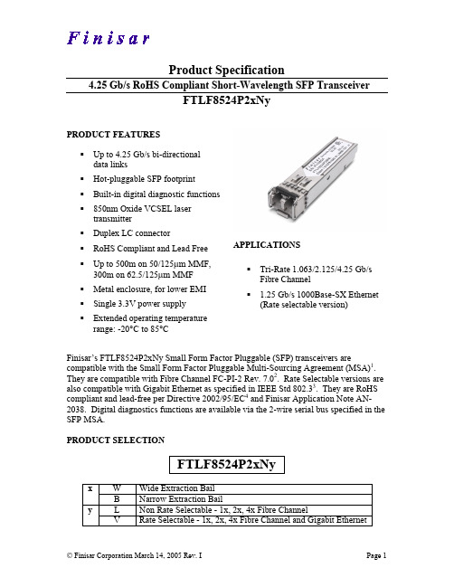
F i n i s a rProduct Specification1000BASE-T Copper SFP TransceiverFCLF-8520/8521-3Product Features•Up to 1.25Gb/s bi-directional data links •Hot-pluggable SFP footprint •Extended case temperaturerange (0°C to +85°C )•Fully metallic enclosure for low EMI •Low power dissipation (1.05 W typical) •Compact RJ-45 connector assembly •RoHS compliant and Lead Free •Access to physical layer IC via 2-wire serial bus•10/100/1000 BASE-T operation in host systems with SGMII interfaceApplications• 1.25 Gigabit Ethernet over Cat5 cableFinisar’s FCLF-8520/8521-3 1000BASE-T Copper Small Form Pluggable (SFP)transceivers are based on the SFP Multi Source Agreement (MSA)1. They are compatiblewith the Gigabit Ethernet and 1000BASE-T standards as specified in IEEE Std 802.32.The 1000BASE-T physical layer IC (PHY) can be accessed via I2C, allowing access toall PHY settings and features.The FCLF-8520-3 uses the SFP’s RX_LOS pin for link indication, and 1000BASE-Xauto-negotiation should be disabled on the host system. The FCLF-8521-3 is compatiblewith 1000BASE-X auto-negotiation, but does not have a link indication feature(RX_LOS is internally grounded). See AN-2036, “Frequently Asked QuestionsRegarding Finisar’s 1000BASE-T SFPs”, for a more complete explanation on thedifferences between the two models and details on applications issues for the products.PRODUCT SELECTIONPart Number Link Indicator on RX_LOS Pin 1000BASE-X auto-negotiationenabled by defaultFCLF-8520-3 Yes No FCLF-8521-3 No YesI.SFP to Host Connector Pin OutPin Symbol Name/Description Note 1 V EET Transmitter ground (common with receiver ground) 1 2 T FAULT Transmitter Fault. Not supported 3 T DIS Transmitter Disable. PHY disabled on high or open 2 4 MOD_DEF(2) Module Definition 2. Data line for serial ID 3 5 MOD_DEF(1)Module Definition 1. Clock line for serial ID 3 6 MOD_DEF(0) Module Definition 0. Grounded within the module 3 7 Rate Select No connection required 8 LOS Loss of Signal indication. 4 9 V EER Receiver ground (common with transmitter ground) 1 10 V EER Receiver ground (common with transmitter ground) 1 11 V EER Receiver ground (common with transmitter ground) 1 12 RD- Receiver Inverted DATA out. AC coupled 13 RD+ Receiver Non-inverted DATA out. AC coupled 14 V EER Receiver ground (common with transmitter ground) 1 15 V CCR Receiver power supply 16 V CCT Transmitter power supply 17 V EET Transmitter ground (common with receiver ground) 1 18 TD+ Transmitter Non-Inverted DATA in. AC coupled 19 TD- Transmitter Inverted DATA in. AC coupled 20 V EET Transmitter ground (common with receiver ground) 1 Notes: 1. Circuit ground is connected to chassis ground2. PHY disabled on T DIS > 2.0V or open, enabled on T DIS < 0.8V3. Should be pulled up with4.7k – 10k Ohms on host board to a voltage between 2.0 V and 3.6 V. MOD_DEF(0) pulls line low to indicate module is plugged in.4. LVTTL compatible with a maximum voltage of 2.5V. Not supported on FCLF-8521-3.Table 1. SFP to host connector pin assignments and descriptions1234567891020191817161514131211Towards ASICTowards BezelFigure 1. Diagram of host board connector block pin numbers and namesII. +3.3V Volt Electrical Power InterfaceThe FCLF-8520/8521-3 has an input voltage range of 3.3 V +/- 5%. The 4 V maximum voltage is not allowed for continuous operation.+3.3 Volt Electrical PowerInterfaceUnitsMaxNotes/ConditionsTypParameter SymbolMinSupply Current I s320 375 mA 1.2W max power overfull range of voltageand temperature.See caution note belowInput Voltage V cc 3.13 3.3 3.47 V ReferencedGNDtoMaximum Voltage V max 4 VSurge Current I surge30 mA Hot plug above steady statecurrent. See caution notebelowCaution: Power consumption and surge current are higher than the specified values in the SFP MSATable 2. +3.3 Volt electrical power interfaceIII. Low-Speed SignalsMOD_DEF(1) (SCL) and MOD_DEF(2) (SDA), are open drain CMOS signals (see section VII, “Serial Communication Protocol”). Both MOD_DEF(1) and MOD_DEF(2)must be pulled up to host_Vcc.Low-Speed Signals,Electronic CharacteristicsNotes/ConditionsUnitsParameter SymbolMin MaxSFP Output LOW V OL0 0.5 V 4.7k to 10k pull-up to host_Vcc,measured at host side of connectorSFP Output HIGH V OH host_Vcc - 0.5host_Vcc + 0.3V 4.7k to 10k pull-up to host_Vcc,measured at host side of connectorSFP Input LOW V IL0 0.8 V 4.7k to 10k pull-up to Vcc,measured at SFP side of connectorSFP Input HIGH V IH 2 Vcc + 0.3 V 4.7k to 10k pull-up to Vcc,measured at SFP side of connectorTable 3. Low-speed signals, electronic characteristicsIV. High-Speed Electrical InterfaceAll high-speed signals are AC-coupled internally.High-Speed ElectricalInterface,Transmission Line-SFPParameter SymbolMinTypMaxUnitsNotes/Conditions Line Frequency f L 125 MHz5-levelencoding,perIEEE 802.3Tx Output Impedance Z out,TX100 Ohm Differential, for allfrequencies between1MHz and 125MHzRx Input Impedance Z in,RX100 Ohm Differential, for allfrequencies between1MHz and 125MHzTable 4. High-speed electrical interface, transmission line-SFPHigh-Speed Electrical Interface,Host-SFPParameter SymbolMinTypMax UnitsNotes/ConditionsSingle ended data input swing V insing250 1200mV SingleendedSingle ended data output swing V outsing350 800 mV SingleendedRise/Fall Time T r,T f 175 psec 20%-80% Tx Input Impedance Z in 50 OhmSingleended Rx Output Impedance Z out 50 OhmSingleendedTable 5. High-speed electrical interface, host-SFPV. General SpecificationsNotes:GeneralParameter Symbol Min Typ Max Units Notes/Conditions Data Rate BR 10 1,000Mb/sec IEEE 802.3 compatible.See Notes 2 through 4 belowCable Length L 100 m Category 5 UTP. BER <10-12Table 6. General specifications1. Clock tolerance is +/- 50 ppm2. By default, the FCLF-8520/8521-3 is a full duplex device in preferred master mode3. Automatic crossover detection is enabled. External crossover cable is not required4. 10/100/1000 BASE-T operation requires the host system to have an SGMII interface with no clocks, and the module PHY to be configured per Application Note AN-2036. With a SERDES that does not support SGMII, the module will operate at 1000BASE-T only.VI. Environmental SpecificationsThe FCLF-8520/8521-3 has an extended range from 0°C to +85°C case temperature as specified in Table 8.Environmental SpecificationsParameter Symbol Min Typ Max Units Notes/Conditions Operating Temperature T op 0 85 °C Case temperature Storage Temperature T sto -40 85 °C Ambient temperatureTable 7. Environmental specificationsVII. Serial Communication ProtocolAll Finisar SFPs support the 2-wire serial communication protocol outlined in the SFP MSA 1. These SFPs use an Atmel AT24C01A 128 byte E 2PROM with an address of A0h. For details on interfacing with the E 2PROM, see the Atmel data sheet titled “AT24C01A/02/04/08/16 2-Wire Serial CMOS E 2PROM.”3The 1000BASE-T physical layer IC can also be accessed via the 2-wire serial bus at address ACh. For details interfacing with the PHY IC, see Marvell data sheet titled “Alaska Ultra 88E1111 Integrated Gigabit Ethernet Transceiver”4 (Marvell document number MV-S100649-00).Serial Bus Timing RequirementsParameter Symbol Min TypMax Units Notes/Conditions I 2C Clock Rate0 100,000Hz Table 8. Serial bus timing requirementsVIII. Mechanical SpecificationsThe host-side of the FCLF-8520/8521-3 conforms to the mechanical specifications outlined in the SFP MSA 1. The front portion of the SFP (part extending beyond the face plate of the host) is larger to accommodate the RJ-45 connector. See Figure 2 below for details.Figure 2. FCLF-8520/8521-3 mechanical dimensionsIX. References1. Small Form Factor Pluggable (SFP) Transceiver Multi-Source Agreement (MSA),September 2000. Documentation is currently available at Finisar upon request. 2.IEEE Std 802.3, 2002 Edition. IEEE Standards Department, 2002.4. “AT24C01A/02/04/08/16 2-Wire Serial CMOS E2PROM”, Atmel Corporation.5. “Alaska Ultra 88E1111 Integrated 10/100/1000 Gigabit Ethernet Transceiver”,Marvell Corporation. X. For More InformationFinisar Corporation1389 Moffett Park DriveSunnyvale, CA 94089-1133Tel. 1-408-548-1000Fax 1-408-541-6138sales@。
H00594_RevT中英文版

RESTRICTED SUBSTANCES FOR HARDWAREPRODUCTS硬件产品限用物质Author:Microsoft Environmental ComplianceTeam作者:微软环境符合小组Document:H00594Revision:TDate: February 15, 2010 Distribution:发行Internal Only 仅限内部External All 外部,不限External Restricted 外部受限I f restricted, specify restricted to whom: 如有限制,请注明限于哪些人All CM & CDM Tier 1’sThis document is considered confidential to and is maintained as trade secret by Microsoft Corporation. This document is disclosed pursuant to a non-disclosure agreement and/or other written agreement between the recipient and Microsoft Corporation (collectively, the“Agreement(s)”).Information in this document is restricted to Microsoft authorized recipients only and any reproduction, distribution, or public discussion of this material is subject to the limits described in the Agreement(s) with Microsoft Corporation.Microsoft and its suppliers may have patents, patent applications, trademarks, copyrights, trade secrets and/or other intellectual property rights covering subject matter in this document. Microsoft’s furnishing of this document to recipient does not grant or imply any license to any patents, trademarks, copyrights, trade secrets or other intel lectual property rights, and recipient’s permitted use of any such intellectual property rights, if any, is solely governed by the Agreements.© 2010 Microsoft Corporation. All rights reserved.本文件属于机密文件,并作为微软的商业机密保留。
AO4922资料
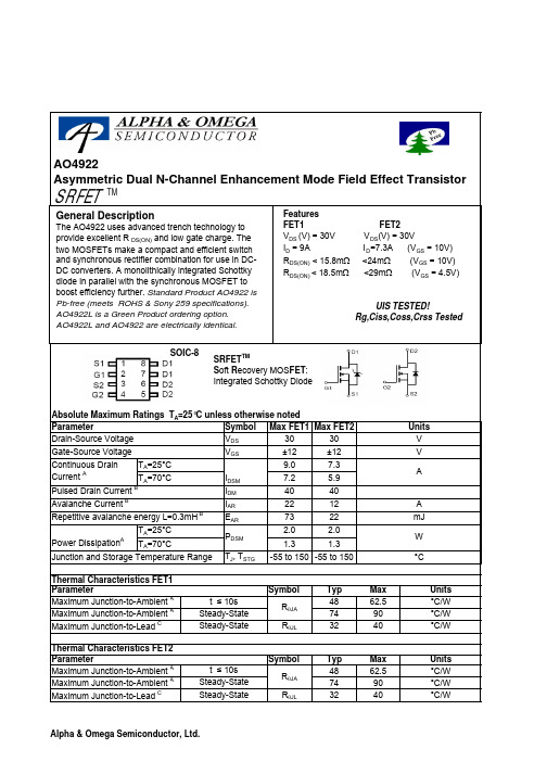
AO4922SOIC-8AO4922SymbolMin TypMaxUnits BV DSS 30V V DS =24V, V GS =0V0.010.1T J =125°C620I GSS 0.1µA V GS(th)Gate Threshold Voltage1.5 1.82.4V I D(ON)40A 1315.8T J =125°C20.225.21518.5m Ωg FS 78S V SD 0.380.5V I S4A C iss 19802574pF C oss 317pF C rss 111pF R g1.32.0ΩQ g (10V)33.043Q g (4.5V)15.0nC Q gs 5.3nC Q gd 6.0nC t D(on) 5.5ns t r 5.5ns t D(off)27.0ns t f 4.3ns t rr 1113ns Q rr7nCTHIS PRODUCT HAS BEEN DESIGNED AND QUALIFIED FOR THE CONSUMER MARKET. APPLICATIONS OR USES AS CRITICAL COMPONENTS IN LIFE SUPPORT DEVICES OR SYSTEMS ARE NOT AUTHORIZED. AOS DOES NOT ASSUME ANY LIABILITY ARISING OUT OF SUCH APPLICATIONS OR USES OF ITS PRODUCTS. AOS RESERVES THE RIGHT TO IMPROVE PRODUCT DESIGN,FUNCTIONS AND RELIABILITY WITHOUT NOTICE.Body Diode Reverse Recovery TimeBody Diode Reverse Recovery Charge I F =9A, dI/dt=300A/µsDrain-Source Breakdown Voltage On state drain currentI D =250uA, V GS =0V V GS =4.5V, V DS =5V V GS =10V, I D =9AReverse Transfer Capacitance I F =9A, dI/dt=300A/µsV DS =V GS I D =250µA FET1 Electrical Characteristics (T J =25°C unless otherwise noted)STATIC PARAMETERS Parameter Conditions I DSS Zero Gate Voltage Drain Current mA V DS =0V, V GS = ±12V Gate-Body leakage current R DS(ON)Static Drain-Source On-ResistanceForward TransconductanceDiode Forward VoltageMaximum Body-Diode + Schottky Continuous CurrentInput Capacitance Output Capacitance DYNAMIC PARAMETERS m ΩV GS =4.5V, I D =7AI S =1A,V GS =0V V DS =5V, I D =9ATurn-On Rise Time Turn-Off DelayTime V GS =10V, V DS =15V, R L =1.7Ω, R GEN =3ΩTurn-Off Fall TimeTurn-On DelayTime Total Gate Charge V GS =10V, V DS =15V, I D =9AGate Drain Charge V GS =0V, V DS =15V, f=1MHz SWITCHING PARAMETERS Total Gate Charge Gate Source Charge Gate resistanceV GS =0V, V DS =0V, f=1MHzA: The value of R θJA is measured with the device in a still air environment with T A =25°C. The power dissipation P DSM and current rating I DSM are based on T J(MAX)=150°C, using t ≤ 10s junction-to-ambient thermal resistance.B: Repetitive rating, pulse width limited by junction temperature T J(MAX)=150°C.C. The R θJA is the sum of the thermal impedence from junction to lead R θJL and lead to ambient.D. The static characteristics in Figures 1 to 6 are obtained using <300 µs pulses, duty cycle 0.5% max.E. These tests are performed with the device mounted on 1 in 2 FR-4 board with 2oz. Copper, in a still air environment with T A =25°C. The SOA curve provides a single pulse rating. Rev0:Sept 2006AO4922AO4922AO4922AO4922SymbolMin TypMaxUnits BV DSS 30V 0.0021T J =55°C5I GSS 100nA V GS(th)0.711.5V I D(ON)40A 2024T J =125°C283523.529m Ω34.748m Ωg FS 26S V SD 0.711V I S2.8A C iss 9001100pF C oss 88pF C rss 65pF R g0.95 1.5ΩQ g 1012nC Q gs 1.8nC Q gd 3.75nC t D(on) 3.2ns t r 3.5ns t D(off)21.5ns t f 2.7ns t rr 16.821ns Q rr8nCTHIS PRODUCT HAS BEEN DESIGNED AND QUALIFIED FOR THE CONSUMER MARKET. APPLICATIONS OR USES AS CRITICAL COMPONENTS IN LIFE SUPPORT DEVICES OR SYSTEMS ARE NOT AUTHORIZED. AOS DOES NOT ASSUME ANY LIABILITY ARISING OUT OF SUCH APPLICATIONS OR USES OF ITS PRODUCTS. AOS RESERVES THE RIGHT TO IMPROVE PRODUCT DESIGN,FUNCTIONS AND RELIABILITY WITHOUT NOTICE.Body Diode Reverse Recovery Time Body Diode Reverse Recovery ChargeI F =7.3A, dI/dt=100A/µsDrain-Source Breakdown Voltage On state drain currentI D =250µA, V GS =0V V GS =2.5V, I D =5AV GS =4.5V, V DS =5V V GS =10V, I D =7.3AReverse Transfer Capacitance FET2 Electrical Characteristics (T J =25°C unless otherwise noted)STATIC PARAMETERS ParameterConditions I DSS µA Gate Threshold Voltage V DS =V GS I D =250µA V DS =24V, V GS =0VV DS =0V, V GS = ±12V Zero Gate Voltage Drain Current Gate-Body leakage current R DS(ON)Static Drain-Source On-ResistanceForward TransconductanceDiode Forward Voltage I F =7.3A, dI/dt=100A/µs V GS =0V, V DS =15V, f=1MHz SWITCHING PARAMETERS Total Gate Charge V GS =4.5V, V DS =15V, I D =7.3AGate Source Charge Gate Drain Charge Turn-On Rise Time Turn-Off DelayTime V GS =10V, V DS =15V, R L =2Ω, R GEN =6ΩTurn-Off Fall TimeMaximum Body-Diode Continuous CurrentInput Capacitance Output Capacitance Turn-On DelayTime DYNAMIC PARAMETERS Gate resistanceV GS =0V, V DS =0V, f=1MHzm ΩV GS =4.5V, I D =6A I S =1A,V GS =0V V DS =5V, I D =7.3AA: The value of R θJA is measured with the device mounted on 1in 2 FR-4 board with 2oz. Copper, in a still air environment with T A =25°C. The value in any given application depends on the user's specific board design. The current rating is based on the t ≤ 10s thermal resistance rating.B: Repetitive rating, pulse width limited by junction temperature.C. The R θJA is the sum of the thermal impedence from junction to lead R θJL and lead to ambient.D. The static characteristics in Figures 1 to 6 are obtained using <300 µs pulses, duty cycle 0.5% max.E. These tests are performed with the device mounted on 1 in 2FR-4 board with 2oz. Copper, in a still air environment with T A =25°C. The SOA curve provides a single pulse rating. Rev 0 : Sept 2006AO4922AO4922。
GI852中文资料
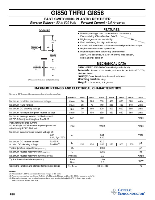
GI850 THRU GI858FAST SWITCHING PLASTIC RECTIFIERReverse Voltage -50 to 800 Volts Forward Current -3.0 AmperesFEATURES♦Plastic package has Underwriters Laboratory Flammability Classification 94V-0♦High surge current capability ♦Fast switching for high efficiency♦Construction utilizes void-free molded plastic technique ♦High forward current operation♦High temperature soldering guaranteed:250°C/10 seconds, 0.375" (9.5mm) lead length,5 lbs (2.3kg) tensionMECHANICAL DATACase:JEDEC DO-201AD molded plastic bodyTerminals:Plated axial leads, solderable per MIL-STD-750,Method 2026Polarity:Color band denotes cathode end Mounting Position:AnyWeight:0.04 ounce, 1.1 gramsMAXIMUM RATINGS AND ELECTRICAL CHARACTERISTICSRatings at 25°C ambient temperature unless otherwise specified.SYMBOLS GI850GI851GI852GI854GI856GI858UNITSMaximum repetitive peak reverse voltage V RRM 50100200400600800Volts Maximum RMS voltage V RMS 3570140280420510Volts Maximum DC blocking voltageV DC 50100200400600800Volts Maximum non-repetitive peak reverse voltage V RSM 75150250450650880Volts Maximum average forward rectified current 0.375" (9.5mm) lead length at T A =90°C I (AV) 3.0Amps Peak forward surge current8.3ms single half sine-wave superimposed on rated load (JEDEC Method)I FSM100.0AmpsMaximum instantaneous forward voltage at:3.0AV F 1.25Volts 9.4A, T J =175°C 1.10Maximum DC reverse current T A =25°C 10.0at rated DC blocking voltage T A =100°CI R 150150200250300500µA Typical junction capacitance (NOTE 1)C J 28.0pF Maximum reverse recovery time (NOTE 2) t rr 200.0ns Maximum reverse recovery current (NOTE 2)I RM(REC) 2.0Amps Typical thermal resistance (NOTE 3)R ΘJA 22.0R ΘJL 8.0°C/W Operating junction and storage temperature rangeT J , T STG-50 to +150°CNOTES :(1) Measured at 1.0 MHz and applied reverse voltage of 4.0 Volts(2) Reverse recovery test conditions: I F =1.0A, V R =30V, di/dt=50A/µs, and I rr =10% I RM for measurement of t rr (3) Thermal resistance from junction to ambient and from junction to lead at 0.375” (9.5mm) lead length,with both leads equally heat sink4/98Dimensions in inches and (millimeters)1101001002000.40.60.8 1.0 1.2 1.4 1.6 1.80.010.11101003070901101301501702.06.08.0110100101004.0010500204060801000.011100.1RATINGS AND CHARACTERISTIC CURVES GI850 THRU GI858FIG.1 - FORWARD CURRENT DERATING CURVETEMPERATURE, °CA V E R A G E F O R W A R D R E C T I F I E D C U R R E N T , A M P E R E SRESISTIVE OR INDUCTIVE LOADFIG. 3 - TYPICAL INSTANTANEOUS FORWARDCHARACTERISTICSP E A K F O R W A R D S U R G E C U R R E N T , A M P E R E SNUMBER OF CYCLES AT 60 H ZT J =25°C f=1.0 MHz Vsig=50mVp-pFIG. 2 - MAXIMUM PEAK FORWARD SURGE CURRENTINSTANTANEOUS FORWARD VOLTAGE,VOLTSJ U N C T I O N C A P A C I T A N C E , p FFIG. 4 - TYPICAL REVERSE CHARACTERISTICSPERCENT OF RATED PEAK REVERSEVOLTAGE, %FIG. 5 - TYPICAL JUNCTION CAPACITANCEREVERSE VOLTAGE, VOLTSI N S T A N T A N E O U S R E V E R S E C U R R E N T M I C R O A M P E R E SNON-REPETITIVE8.3ms SINGLE HALF SINE-WAVE (JEDEC Method)T J =50°C0.8 x 0.8 x 0.40”(20 x 20 x 1mm) COPPER HEATSINKST J =100°CI N S T A N T A N E O U S F O R W A R D C U R R E N T A M P E R E ST J =25°CPULSE WIDTH=300µs 1% DUTY CYCLET L =LEAD TEMPERATURET A =AMBIENT TEMPERATURE REPETITIVET J =25°CT J =150°CT J =25°CT J =150°C T J =25°CL=LEAD LENGTHL=0.375” (9.5mm)LEAD LENGTH0.375” (9.5mm)LEAD LENGTHL=0.25” (6.3 mm)。
PC852中文资料
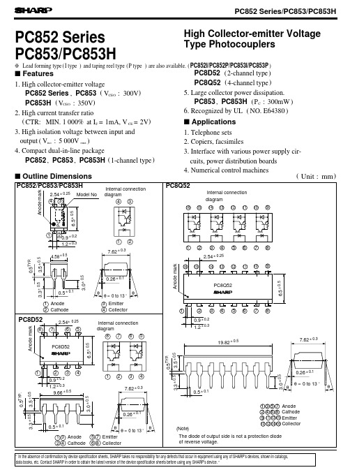
PC853/PC853HPC852 Series s Applicationss Features1. High collector-emitter voltage2. High current transfer ratio3. High isolation voltage between input and output (V iso4. Compact dual-in-line package5. Large collector power dissipation.6. Recognized by UL 1. Telephone sets 2. Copiers, facsimiles3. Interface with various power supply cir- cuits, power distribution boards4. Numerical control machinesF =1mA, V CE =2V )()PC852, PC853, PC853H (1-channel type )PC852 Series , PC853 (V CEO :300V ) PC853H (V CEO :350V ) PC8D52 (2-channel type ) PC8Q52 (4-channel type ) PC853, PC853H (P C :300mW )High Collector-emitter Voltage Type Photocouplers(CTR:MIN. 1 000% at I g Lead forming type (I type ) and taping reel type (P type ) are also available. (PC852I/PC852P/PC853I/PC853P ):5 000V rms )(NO. E64380)0-301002550751001252030405060Fig. 1 Forward Current vs. Ambient TemperatureAmbient temperature T a (˚C )0012510020050150255075100-30-250255075100125050100150200250300350C o l l e c t o r p o w e r d i s s i p a t io n P C (m W )Ambient temperature T a (˚C )Duty ratio55Pulse width <=100µs 102010050200500210-310-25210-1525Fig. 3 Peak Forward Current vs. Duty RatioP e a k f o r w a r d c u r r e n t I F M (m A )20.51.01.52.02.53.03.551020501002005001Forward voltage V F (V )Fig. 4 Forward Current vs. Forward Voltage00.1C u r r e n t t r a n s f e r r a t i o C T R (%)0.20.510125Forward current I F (mA )Ambient TemperatureAmbient TemperatureF o r w a r d c u r r e n t I F (m A )(PC852 Series )C o l l e c t o r p o w e r d i s s i p a t i o n P C (m W )(PC853/PC853H )F o r w a r d c u r r e n t I F (m A )(PC852 Series )Forward CurrentFig. 2-a Collector Power Dissipation vs.Fig. 2-b Collector Power Dissipation vs.Fig. 5-a Current Transfer Ratio vs. 1V CE =2V T a =25˚CAmbient temperature T a (˚C )10 0005 0002 0001 000T a =25˚C5 0004 0003 0002 0001 000Forward current I F (mA )00.1C u r r e n t t r a n s f e r r a t i o C T R (%)0.20.51251000100200123450.5mA1mA1.5mA 2mA2.5mA3mA 5mA Collector-emitter VoltageC o l l e c t o r c u r r e n t I C (m A )Collector-emitter voltage V CE (V )0010020012345C o l l e c t o r c u r r e n t I C (m A )Collector-emitter voltage V CE (V )Collector-emitter Voltage204060801005001001500R e l a t i v e c u r r e n t t r a n s f e r r a t i o (%)0-300.20204060801000.40.60.81.01.2Fig. 8 Collector-emitter SaturationVoltage vs. Ambient TemperatureAmbient temperature T a (˚C )C E (s a t ) (V )2004060-118010010-1010-910-810-710-610-5Fig. 9 Collector Dark Current vs.Ambient TemperatureC o l l e c t o r d a r k c u r r e n t I C E O (A )Ambient temperature T a (˚C )Forward Current(PC853/PC853H )(PC852 Series )(PC853/PC853H )P C (MAX.)Fig. 5-b Current Transfer Ratio vs.Fig. 6-a Collector Current vs.Fig. 6-b Collector Current vs.Fig. 7 Relative Current Transfer Ratio vs. Ambient TemperatureAmbient Temperature T a (˚C )C o l l e c t o r -e m i t t e r s a t u r a t i o n v o l t a g e V 0.5mA1mA1.5mA2mA2.5mA3mA5mAV CE =2V T a =25˚CT a =25˚CI F =10mA T a =25˚CP C (MAX.)I F =10mAI F =1mAV CE =2VI F =20mA I C =100mAV CE =200V5 0004 0003 0002 0001 000-30-3010R e s p o n s e t i m e (µs )2151020501002005000.010.1110Fig.11 Frequency ResponseFrequency f (kHz )00.1110100100Ω10ΩV o l t a g e g a i n A v (d B )C o l l e c t o r -e m i t t e r s a t u r a t i o n v o l t a g e V C E (s a t )(V )Forward current I F (mA )12345Fig.12 Collector-emitter Saturation Voltage vs. Forward CurrentV CE =2V I C =20mA T a =25˚Ct rt ft d t s V CE =2V I C =20mA T a =25˚CR L =1k Ω1 000 1 000-25-20-15-10-5Please refer to the chapter “Precautions for Use ”Fig.10 Response Time vs. Load ResistanceLoad resistance R L (k Ω)q。
A4989SLDTR-T;中文规格书,Datasheet资料
Selection Guide
Part Number A4989SLDTR-T Packing Tape and reel, 4000 pieces per reel
Absolute Maximum Ratings
Characteristic Supply Voltage Logic Supply Voltage Logic Inputs and Outputs SENSEx pins Sxx pins LSSx pins GHxx pins GLxx pins Cxx pins Operating Ambient Temperature Junction Temperature Storage Temperature TA TJ(max) Tstg Range S Symbol VBB VDD Notes Rating –0.3 to 50 –0.3 to 7 –0.3 to 7 –1 to 1 –2 to 55 –2 to 5 Sxx to Sxx+15 –2 to 16 –0.3 to Sxx+15 –20 to 85 150 –55 to 150 Units V V V V V V V V V ºC ºC ºC
The above-supply voltage required for the high-side N-channel MOSFETs is provided by a bootstrap capacitor. Efficiency is enhanced by using synchronous rectification and the power FETs are protected from shoot-through by integrated crossover control and programmable dead time.
S1T8528资料
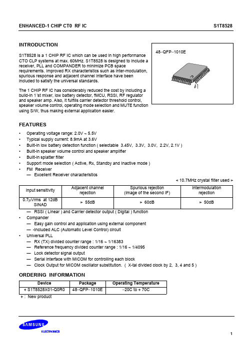
ORDERING INFORMATION
Device + S1T8528X01-Q0R0 + : New product Package 48−QFP−1010E Operating Temperature −20C to + 70C
1
元器件交易网
S1T8528
ENHANCED-1 CHIP CT0 RF IC
元器件交易网
ENHANCED-1 CHIP CT0 RF IC
S1T8528
INTRODUCTION
S1T8528 is a 1 CHIP RF IC which can be used in high performance CTO CLP systems at max. 60MHz. S1T8528 is designed to include a receiver, PLL and COMPANDER to minimize PCB space requirements. Improved RX characteristics such as inter-modulation, spurious response and adjacent channel interface have been included to satisfy the universal standards. The 1 CHIP RF IC has considerably reduced the cost by including a build-in 1’st mixer, low battery detector, fMCU, RSSI, RF regulator and speaker amp. Also, it fulfills carrier detector threshold control, speaker volume control, operating mode selection and MUTE function using S/W, thus making external application easier. 48−QFP−1010E
- 1、下载文档前请自行甄别文档内容的完整性,平台不提供额外的编辑、内容补充、找答案等附加服务。
- 2、"仅部分预览"的文档,不可在线预览部分如存在完整性等问题,可反馈申请退款(可完整预览的文档不适用该条件!)。
- 3、如文档侵犯您的权益,请联系客服反馈,我们会尽快为您处理(人工客服工作时间:9:00-18:30)。
♦ Features
• Bit rate : ~ 2.5 Gbps
• Packaging : TO-18 with 5-leads • Light wave length : 1.3 µm/1.55 µm • Fiber pigtail : 9.5 µm/125 µm SM fiber • High performance APD
• Low noise GaAs preamplifier IC • High sensitivity ~ -33 dBm
• AGC with proper time constant
♦ Applications
• High-speed optical transmission systems for OC-48/STM-16 (2.5 Gbps) and measurement instruments
♦ Functional Description
The F085 series APD-preamplifier modules are capable receiver modules with a minia-turized size and a low cost for use in the standard SONET/SDH systems. An APD is utilized to achieve extremely high sensitivity. A low noise GaAs preamplifier is built in to obtain high sensitivity and a stable operation. Differential outputs and a function of photocurrent moni-toring are available with employing the 5-lead TO-18 package.
The F0852491T is applicable for 1.3 µm/1.55 µm optical fiber communication systems for OC-48/STM-16 (2.5 Gbps), typically showing 10 dB higher sensitivity than that of the F0812484T.
02.04.24
Advance
APD Preamplifier Module
5 V Supply / 2.5 Gbps NRZ
F0852491T
♦ Block Diagram
♦ Absolute Maximum Ratings
All published data at Tc=25°C unless otherwise indicated. This device isn't guaranteed opto-electric characteristics in these range. At least, this device isn't broken in these range.
Tc=25 °C
V
C 1
OUT
OUT
APD diameter=35 um, C 1=200 pF, C 2=470 pF
Parameter
Supply Voltage
Symbol V CC
Min.4.75
Max.5.25
Units V
typ.5.00
Parameter
Supply Voltage Circuit Current APD Voltage APD Current
Operating Case Temperature Storage Temperature
Symbol V CC I CC V APD I APD Tc Tstg
Value V EE -0.5 ~ V EE +7
700 ~ V BR
2-20 ~ +85-40 ~ +90
Units V mA V mA °C °C
♦ Recommended Operating Conditions
Pins are identified by LABEL.
Unit : mm ♦ Opto-Electrical Characteristics
Tc=25 °C, V CC =+5.0 V, V EE =GND, λ=1310nm, unless specified
♦ Package Drawings
Parameter
Symbol
Test Conditions
Value Units
Min.
Typ.Max.Breakdown Voltage V BR I APD =100 µA
506877V Circuit Current I CC DC
284862mA Responsively R Pin=-30 dBm
M=1
-0.85-A/W Transimpedance Zt Pin=-30 dBm,M=10R L =50Ω, f=100 MHz
- 2.0-k ΩBandwidth
fc -3dB, M=10Pin=-30 dBm
- 1.9 -GHz Equivalent Input Noise Current Density Inoise f=100 MHz - 5.5-pA/√Hz Sensitivity
Pin min --33-dBm Maximum Optical Input Power Pin max --5-dBm Low Frequency of cut-off
f CL
C 2=470pF
-17
-kHz PRBS223-12.48832 Gbps BER=1E-10
♦ Typical Characteristics
(1)Eye Diagrams (Tc=25 °C, 50Ω Load) 2.488Gbps NRZ, PRBS 223-1, λ=1.3µm
1.00E+06 1.00E+07 1.00E+08 1.00E+09 1.00E+10
Frequency[Hz]
T r a n s i m p e d a n c e [d B Ω]
(2) Frequency Response (Tc=25 °C, 50Ω Load, Pin=-30dBm)
12m V /d i V
Average Input Optical Power : -30dBm, M=10
(4) Temperature Dependence of Breakdown Voltage
40
45
50
55
60
65
20
40
60
80
Temperature [°C]
B r e a k d o w n V o l t a g e [V ]
(3) Bit Error Rate Curve (Tc=25°C)
10-3
10-4
10-510-610-710-810-910-1010-1110-12
-36-34Average Received Power[dBm]
B i t E r r o r R a t
e
-38-32
-40
Electron Device Department
♦ Package Option
To Package
ROSA
LC receptacle
CC OUTB
UNIT : mm。