RST150524中文资料
芯片手册
功能简述 ............................................................................ 26 编程指南 ............................................................................ 26 载波通信的工作步骤 .................................................................. 27 寄存器 .............................................................................. 28
9) ISO7816 功能 ........................................................... 41
功能简述 ............................................................................ 41 编程指南 ............................................................................ 41 寄存器 .............................................................................. 42
4) LCD/LED显示驱动 ........................................................ 32
SN54LS123中文资料

RETRIGGERABLE MONOSTABLE MULTIVIBRATORSThese dc triggered multivibrators feature pulse width control by three meth-ods. The basic pulse width is programmed by selection of external resistance and capacitance values. The LS122 has an internal timing resistor that allows the circuits to be used with only an external capacitor. Once triggered, the ba-sic pulse width may be extended by retriggering the gated low-level-active (A)or high-level-active (B) inputs, or be reduced by use of the overriding clear.•Overriding Clear Terminates Output Pulse•Compensated for V CC and T emperature Variations•DC Triggered from Active-High or Active-Low Gated Logic Inputs •Retriggerable for Very Long Output Pulses, up to 100% Duty Cycle •Internal Timing Resistors on LS122SN54/74LS122 (TOP VIEW)(SEE NOTES 1 THRU 4)SN54/74LS123 (TOP VIEW)(SEE NOTES 1 THRU 4)NOTES:1.An external timing capacitor may be connected between C ext and R ext /C ext (positive).2.To use the internal timing resistor of the LS122, connect R int to V CC .3.For improved pulse width accuracy connect an external resistor between R ext /C ext and V CC with R int open-circuited.4.To obtain variable pulse widths, connect an external variable resistance between R int /C ext and V CC .R ext/CR ext/C ext 11ĂRext/2CLRC extNC Ċ NO INTERNAL CONNECTION.。
RST数字仪表选型手册
RST112-U
单相电压
RST112-dU RST112-P
一路直流电压 单相电流、电压、有功功率
面框:48×48
RST112-Q RST112-F
单相电流、电压、无功功率 电压频率
开孔:45.5×45.5
RST112-K
功率因数
RST112-W
单相电流、电压、有功电度
RST112-V
单相电流、电压、无功电度
测量参数 三相电流 三相电压 三相有功功率 三相无功功率 电压频率 功率因数
3FBMDPEF
面框、开孔(mm)
面框:96×48 开孔:90×44
面框、开孔(mm) 面框:48×48 开孔:45.5×45.5
面框、开孔(mm) 面框:96×96 开孔:85×85
3
成都瑞科电气有限公司
Realcode
成都瑞科电气有限公司
2
RST 系列数字电力仪表
RST200 系列数字电测仪表型号列表
RST210 系列单相数字电测仪表
产品图片
仪表型号
RST210-I
RST210-dI
RST210-U
RST210-dU
RST210-P
RST210-Q
RST210-F
RST210-K
选型案例:RST210-I,数码管显示、单相电流 RST210-P,数码管显示、单相有功功率
RTS-1505中文资料
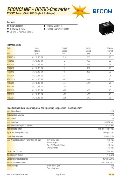
ECONOLINE - DC/DC-Converter
RTS/RTD Series, 2 Watt, SMD (Single & Dual Output) Package Style and Pinning (mm)
Dual Output Single Output
3rd angle projection
元器件交易网
ECONOLINE - DC/DC-Converter
RTS/RTD Series, 2 Watt, SMD (Single & Dual Output) Features
● ● ●
1kVDC Isolation Efficiency to 70% UL 94V-0 Package Material
Recommended Footprint Details
Pin Connections
10 12.70 1 2
Hale Waihona Puke 7 12.70 4 5 1.20 1.80
8 1 2
5 4 1.20 1.80
Pin # Single 1 –Vin 2 +Vin 4 –Vout 5 +Vout 7 No Pin 8 NC 10 No Pin NC = No Connection
2.54
RTD-0505 RECOM ****
0.50±0.5
2.57
RTS-0505 RECOM ****
0.50±0.5
15.24 14.84 7.05 1.65 7.05 1.65
12.75 12.40
9.30 9.00
0.20 2.54x4
0.20 2.54x3 8.60 10.00 11.80
RST2使用手册

☆ ☆
☆
由于产品的改进,手册内容可能变更,恕不另行通知。 驱动器及电机内不附带任何维修配件,请勿私自拆卸;对驱动器及电机 的任何改动将使其保修权利失效; 本公司也不对由此引起的后果承担任 何责任。 阅读本手册前,请遵守以下安全防范说明。
安全防范说明
以下为此说明中将用到的警示标志 ———— ————
危险:表示错误的操作将可能导致人员伤亡! 注意:表示错误的操作将可能对人员造成伤害并损 坏设备或产品!
锐普德数控
RST系列交流伺服驱动器用户手册
非常感谢您选购和使用本公司交流伺服驱动器 请爱惜、爱护本产品! 在使用本驱动器之前,请务必仔细阅读本手册,按照所示规范进行操作使用
前 言
本说明书主要为用户提供驱动器的使用方法、系统参数、技术指标。由于 使用不当或错误的操作,可能会导致意外事故发生并影响产品的性能和使用寿 命,为使本产品更好地发挥其性能和更好地为您服务,请您在使用前认真阅读 本说明书。 在产品使用过程中如遇到任何不解,请查阅本说明书或拨打我们的技术支 持电话025-83328880。请您将对交流伺服驱动器的意见和更高要求告知我们, 我们会竭诚为您服务。
ii
锐普德数控
RST系列交流伺服驱动器用户手册
伺服电机 U、V、W 端子不可反接,不可接交流电源。 不可通过调换 U、V、W 端子改变电机转向。 伺服电机与伺服驱动器之间须直连,不能接入电容、电感或滤波器。 并接在输出信号直流继电器上的续流二极管不可接反。 通电前确认伺服驱动器和伺服电机已安装妥善,固定牢固,电源电压及接线 正确。 调试时伺服电机应先空载运转,确认参数设置无误后,再作负载调试,防止 因错误的操作导致机械和设备损坏。 应接入一个紧急停止电路,确保发生事故时,设备能立即停止运转,电源立 即被切断。 在复位一个报警之前,必须确认运行信号关断,否则会突然再启动。 伺服驱动器必须与规定的伺服电机配套使用。 附近有电磁干扰时,伺服驱动器电源接入隔离变压器和滤波器。 不要频繁接通、断开伺服系统电源,防止损坏系统。 伺服驱动器和伺服电机连续运转后可能发热,运行时和断电后的一段时间 内,不能触摸驱动器散热器和电机。
PCS-222B-I_X_说明书_国内中文_国内标准版_X_R1.01
我们对本文档及其中的内容具有全部的知识产权。除非特别授权,禁止复制或向第三方分发。凡侵犯本公司版权等知识产权的,本公司必 依法追究其法律责任。 我们定期仔细检查本文档中的内容,在后续版本中会有必要的修正。但不可避免会有一些错误之处,欢迎提出改进的意见。 我们保留在不事先通知的情况下进行技术改进的权利。
i
PCS-222B-I 智能终端 残余电压
在装置电源关闭后,直流回路中仍然可能存在危险的电压。这些电压需在数秒钟后才会消失。
警示!
接地 装置的接地端子必须可靠接地。
运行环境 该装置只允许运行在技术参数所规定的大气环境中,而且运行环境不能存在不正常的震动。
额定值 在接入交流电压电流回路或直流电源回路时,请确认他们符合装置的额定参数。
本手册中将会用到以下指示标记和标准定义:
危险! 意味着如果安全预防措施被忽视,则会导致人员死亡,严重的人身伤害,或 严重的设备损坏。
警告! 意味着如果安全预防措施被忽视,则可能导致人员死亡,严重的人身伤害, 或严重的设备损坏。
警示! 意味着如果安全预防措施被忽视,则可能导致轻微的人身伤害或设备损坏。 本条特别适用于对装置的损坏及可能对被保护设备的损坏。
P/N:ZL_PCS-222B-I_X_说明书_国内中文_国网标准版_X
购买产品,请联系: 电话:025-87178911 传真:025-52100511、025-52100512
版本:R1.01
ii
南京南瑞继保电气有限公司
目录
PCS-222B-I 智能终端
前言.................................................................................................................................................... i 目录.................................................................................................................................................. iii 第 1 章 概述...................................................................................................................................... 1
复位电路,13家维第6期
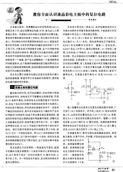
STB- 3.3V
路, V50 1 c 极产 生
复位电压 RST。 开机复位 具体
一句话维修
陆蜂峰
* LG 32LH23UR -CA 型彩电,主板型号为
主P19A EAJ(56856906( 川,蓝色电源指示灯亮,冷机
电回路,防止在极短时间内频繁开/关机复位不正常造
波小。而时钟信号的作用是控制系统的 MCU 是复杂的
数字时序电路,只有在时序脉冲的触发驱动控制下才可
正常工作,才能完成不同的指令功能,这个时序脉冲就
是我们常说的时钟信号,要实现不同功能的控制,就要
有各种不同频率的时钟信号,所以每个 MCU 处理器外 部都接有一个晶振,来产生比较精确的一个基准频率的 时钟振荡脉冲,这个基准时钟根据电路功能的需求在内
Hot line
教你全面认识液晶彩电主板中的复位电路
•
在液晶主板中,负责整机运行的控制系统 (MCU)
宋太颖·
在电视中常见的一种由 RC 延时电路组成的分立
要能正常工作,就必须要保证电源、时钟、复位这几大要
素是正常的。电源部分的作用是为电路提供所需电能, 要提供所需的稳定的直流工作电压,有足够的电流且纹
电@脚 8V 正常,@脚行激励 7 .8V 离电平无输出。由
此判断为 CPU 保护,测 CPU@脚为低电平。依次检 查保护取样电路,发现行 20QV 视放电源取样电阻
R417( 120kn; 1W)开路,换之恢复正常。
为芯片@脚提供复位电压。随着 C507 的充电, V501 b
极电压逐渐升高,当 C507 两端充电完成达到 3 . 3V 时 V501 截止, V501 c 极电压为 OV ,上电复位过程完成 。 关机时(或者 3.3V 掉电时 ) C 507 所充电荷通过
RN8209-SSOP24-天高微 单相计量芯片
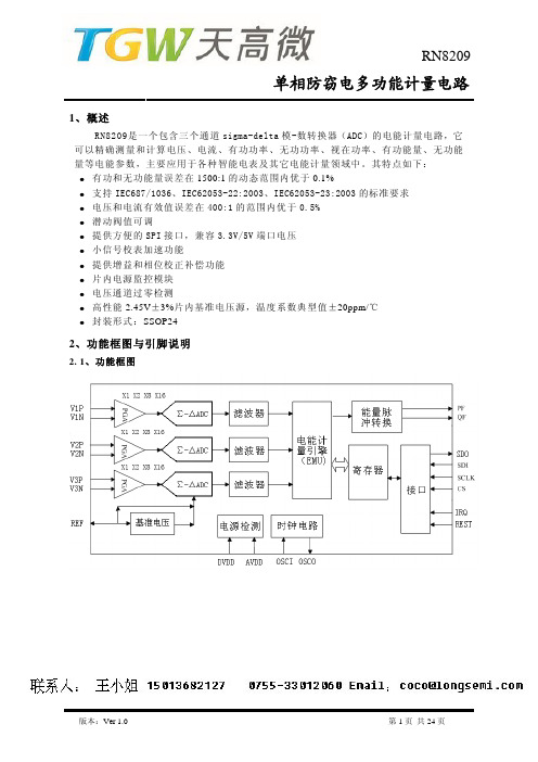
1、 关闭MCU全局中断和/INT中断; 2、 MCU通过串口读RIF寄存器,清IF和RIF寄存器,将IRQ恢复到高电平; 3、 MCU通过判断RIF的中断标志来判断RN8209的中断源,转而执行相应的中断
处理程序;在此过程中,RN8209若发生新的中断事件,IF相关标志置位, IRQ也会由高变低,触发MCU的/INT中断标志置位,记录了此事件;
CS 上升沿之间的时间间隔 t2 要大于等于半个 SCLK 周期。
注意:有写保护功能的寄存器在写操作之前要先写入写使能命令。
4. 4. 4、SPI 读操作
MCU 在 CS 有效后,先通过 SPI 写入命令字节(8bit,包含寄存器地址),RN8209收 到读命令后,在 SCLK 的上升沿将数据按位从 SDO 引脚输出。
3. 在最后一个比特移出 SDO 后,CS 由低至高时将 RIF 寄存器的内容和 IF 同步。
除了读 RIF 寄存器操作,其他情况下 IF 和 RIF 都保持一致。为了在 SPI 读中断标志 过程中不丢失中断,在中断处理程序中推荐用户使用 RIF 寄存器。
版本:Ver 1.0
第 5 页 共 24 页
用于电压采样。ADC 采用全差分方式输入,电流、电压通道最大信号输入幅度峰值为 660mV。芯片测量三个通道的真有效值参数输出,提供两路有功功率、无功功率的计算 和校正。同时提供频率测量、过零检测和能量脉冲输出。 4. 2、能量脉冲输出
RN8209带有专用的有功、无功能量的脉冲输出端口 PF、QF,可以通过这两个端口直 接进行误差比对。PF/QF 输出满足下面的时序关系:
2、功能框图与引脚说明
2. 1、功能框图
版本:Ver 1.0
第 1 页 共 2ቤተ መጻሕፍቲ ባይዱ 页
PC164S40字段式驱动芯片 高抗扰 低功耗

⏹特征●固定的1/4占空比模式,最多144点。
●低功耗设计,典型条件下电流为6uA。
●内置OSC电路●内部LCD对比度控制电路●集成上电复位电路●无需外部组件●接口:2线串口●与TTL/CMOS兼容●高EMC抗扰度⏹应用领域●家电产品●仪表设备等●玩具●PDA●钟表⏹订单信息零件号包装类型卷带式TSSOP-482500/卷⏹引脚说明名称I/O功能SDA I/O162线串行数据输入输出SCL I152线串行时钟输入VSS I12GNDVDD I11逻辑电源VLCD I10LCD偏置电压,默认为低电平。
SEG0~35O18~24,25~35,1~5LCD的部分驱动器输出COM0~3O6~9LCD的公共驱动器输出PC164S404COM段式L CD驱动器PC164S40⏹典型应用电路⏹结构图35PC164S40⏹绝对最大额定值⏹电气特性载。
⏹输入输出端等效电路图VDDT0,T1,T20VDD⏹命令寄存器说明76543210 ADSET C00P[4:0]DISCTL C01FR[1:0]LF SR[1:0] MODSET C10ULP EN/// EVRSET C1100EV[2:0]ICSET C1100P[5]RST/ BLKCTL C1111BF[2:0] APCTL C1111EV[3]AON AOF⏹功能说明●命令和数据传输方法该装置通过两线串行接口传输数据,当命令或数据通过两线串行接口输入时,必须生成“启动条件”和“停止条件”状态。
当设置sda’h’→’l’在scl’h时,它成为“启动条件”。
当设置sda’l’→’h ’在scl’h’时,它就变成了”停止条件”。
SDASCL●1.生成“开始条件”。
2.发出从站地址7C。
3.传输命令。
4.传输显示数据。
5.生成“停止条件”在生成“启动条件”之后,命令传输(command transfer)对从地址进行处理(写模式为“01111100”,读模式为“01111101”)。
RSO-0505S;RSO-0505D;RSO-2412DZ;RSO-2405SZH3;RSO-243.3S;中文规格书,Datasheet资料

ECONOLINEDC/DC-Converterwith 3 year WarrantyRSO E-95REV:1/2011EN-60950-1 Certified EN-60601-1 CertifiedDescriptionHigh-power-density, an industrial temperature range of -40°C to +85°C and extra features like On-Off-control are just some of the characteristics of this converter, ideal for highly sophisticated industrial-designs. The RSO series is available with isolation of 2kV or 3kV by chosing option "/H2"or "/H3" in which case it is also ideal for medical applications which additionally require EN-60601-1 certification. The standard version offers 2:1 input voltage range, while the “Z” version features 4:1input voltage range, which includes an input voltage range covering both 5V and 12V supplies.1 WattSIP8 Isolated Single &Dual Output●2:1 and 4:1 Wide Input Voltage Ranges ●1kVDC, 2kVD or 3kVDC Isolation ●UL94V-0 Package Material●Certified for Medical Applications ●Continuous Short Circuit Protection ●Low Noise●No External Capacitor needed ●Efficiency to 83%FeaturesRegulated ConvertersSelection GuidePart NumberInput Rated Output Output Current Efficiency Max Voltage Range Voltage typ.CapacitiveSIP8(VDC)(VDC)(mA)(%)Load (1)RSO-xx3.3S* 4.5-9**, 9-18 3.330068-723300µF18-36, 36-7270RSO-xx05S* 4.5-9**, 9-18520073-751200µF18-36, 36-7275-78RSO-xx09S* 4.5-9**, 9-18911174-78680µF18-36, 36-7278-81RSO-xx12S* 4.5-9**, 9-18128375-80680µF18-36, 36-7280-83RSO-xx15S* 4.5-9**, 9-18156775-80680µF18-36, 36-7280-83RSO-xx3.3D* 4.5-9**, 9-18±3.3±15068-72±1500µF18-36, 36-7270RSO-xx05D* 4.5-9**, 9-18±5±10073-75±470µF18-36, 36-7275-76RSO-xx09D* 4.5-9**, 9-18±9±5674-78±470µF18-36, 36-7278RSO-xx12D* 4.5-9**, 9-18±12±4275-79±330µF18-36, 36-7279-80RSO-xx15D* 4.5-9**, 9-18±15±3475-79±330µF18-36, 36-7279-80RSO-xx3.3SZ*9-36 3.330068-703300µF18-7270RSO-xx05SZ* 4.5-18**, 9-36520073-781200µF18-7275RSO-xx09SZ* 4.5-18**, 9-36911175-81680µF18-7278RSO-xx12SZ* 4.5-18**, 9-36128377-83680µF18-7280RSO-xx15SZ* 4.5-18**, 9-36156778-83680µF18-7280RSO-xx3.3DZ*9-36±3.3±15070-74±1500µF18-7270RSO-xx05DZ* 4.5-18**, 9-36±5±10073-77±470µF18-7275RSO-xx09DZ* 4.5-18**, 9-36±9±5674-78±470µF18-7278RSO-xx12DZ* 4.5-18**, 9-36±12±4275-80±330µF18-7280RSO-xx15DZ* 4.5-18**, 9-36±15±3475-80±330µF18-7280No suffix is standard isolation (1kVDC) e.g, RSO-0505S*add suffix /H2 or /H3 for 2kVDC or 3kVDC isolation, e.g, RSO-0505S/H2, RSO-0505DZ/H3** derate to 75% if Vin<5V, 12V 4:1 input also requires an external 10µF input capacitor.Refer to Application NotesRoHS2002/95/EC6/6O u t p u t P o w e r (%)100602040Operating Temperature °C80Derating-Graph(Ambient T emperature)2:1Input 4:1Input (RS0-S/D) (RSO-SZ/DZ)xx = 4.5-9Vin = 05 xx = 4.5-18Vin = 12xx = 9-18Vin = 12 xx = 9-36Vin = 24 xx = 18-36Vin = 24 xx = 18-72Vin = 48xx = 36-72Vin = 48/E-96REV: 1/2011R S 0Input Voltage Range 2:1 and 4:1Output Voltage Accuracy ±2% typ.Line Voltage Regulation 2:1±0.2% max.4:1±0.5% max.Load Voltage Regulation 2:1±0.4% max.(10% to 100% full load)4:1±0.5% typ.Minimum Load0%Output Ripple and Noise (20MHz limited)50mVp-p max.Operating Frequency 2:1200kHz min. / 500kHz max.4:1100kHz min. / 800kHz max.Efficiency at Full Load See Selection GuideQuiescent Current RSO-05xxS_D, SZ_DZ 40mA typ.Nominal input Voltage RSO-12xxS_D32mA typ.(Standard, /H2 and /H3)RSO-24xxS_D, SZ_DZ 25mA typ.RSO-48xxS_D, SZ_DZ15mA typ.CTRL Pin drive current /see Notes)3mA typ, 6mA max.Quiescent Input Current when Converter is OFF 10mA max.Isolation Voltage Standard (tested for 1 second)1000VDC(rated for 1 minute)500VAC / 60Hz/H2 Version (tested for 1 second)2000VDC(rated for 1 minute)1000VAC / 60Hz/H3 Version (tested for 1 second)3000VDC(rated for 1 minute)1500VAC / 60HzIsolation Capacitance Standard 2:1 Single 10pF min. / 40pF typ. / 60pF max.Isolation Capacitance /H2 and /H32:1 Single 5pF min. / 30pF typ. / 60pF max.Isolation Capacitance Standard 2:1 Dual 120pF min. / 170pF typ. / 250pF max.Isolation Capacitance /H2 and /H32:1 Dual 5pF min. / 30pF typ. / 60pF max.Isolation Capacitance Standard 4:1 Single/Dual 200pF max.Isolation Capacitance /H2 and /H34:1 Single/Dual 30pF max.Isolation Resistance >1G Ωmin.Short Circuit ProtectionContinuousOperating Temperature Range (free air convection)-40°C to +85°C (see Graph)Storage Temperature Range -55°C to +125°CRelative Humidity 95% RH Package Weight 4.7gPacking Quantity 22 pcs per TubeMTBF (+25°C)using MIL-HDBK 217F 1685 x 103 hours (+85°C)using MIL-HDBK 217F254 x 103 hoursSpecifications (Core Operating Area)measured at T A = 25°C, nominal input voltage, full load and after warm-up time unless otherwise specifiedTypical ApplicationE f f i c i e n c y %100040%0%100%40Efficiency / Load 60%80%20%206080Total Output current (%)RSO-24xxS}Detailed Information seeApplication Notes chapter "MTBF"-Vin-Vout+Vout+VinE f f i c i e n c y %100040%0%100%40Efficiency / Load 60%80%20%206080Total Output current (%)RSO-1205SZ/RSO E-97REV:1/20113rd angleprojection8 PIN SIP PackageXX.X ± 0.5 mm XX.XX ± 0.25 mmPin 8 (NC*)This pin is used internally and must have no external connection.Pin 5 (NC)Not connected internally.Pin 3 (CTRL)This pin provides an Off function which puts the converter into a low power mode. When the pin is ‘high’ the converter is OFF and when the pin is high ‘Z’ the converter is ON. There is no allowed low state for this pin.Package Style and Pinning (mm)Single Output Recommended Footprint DetailsPin Connections Pin #SingleDual1 –Vin –Vin2 +Vin +Vin 3CTRL CTRL 5NC NC 6+Vout +Vout7 –Vout C om8NC*–VoutNC = No ConnectionNC* = NC, but no external Connection allowed.CTRL Examples+VoutCtrlTTL Remote CTRL CircuitVoltage to be applied via a limiting resistor with a recom-mended value of 1K for RSO-05xx; 3.3K for RSO-12xx;4.7K for RSO-24xx and 10K for RSO-48xx.Control Pin Input Current: 10mA Voltage Set Point Accuracy with external input/outputcapacitors refer to typ. ± 1%recommended test circuit: max. ±2%Control Pin (CTRL) Input Current, control voltage applied via 1K resistor,output voltage must typ. 3mA reduce to 0V: max. 6mA+VoutIsolated Remote CTRL CircuitNotes Note 1Maximum capacitive load is defined as the capacitive load that will allow start up in under 1 second without damage to the converterCertifications EN General Safety Report: IL-R7109EN60950-1:2001 + A11:2004EN Medical SafetyReport: PS071001601EN60601-1:1990 + A11:1996/分销商库存信息:RECOM-POWERRSO-0505S RSO-0505D RSO-2412DZ RSO-2405SZ/H3RSO-243.3S RSO-1212S RSO-2412D RSO-2415D RSO-0505S/H2 RSO-2405SZ/H2RSO-2405DZ RSO-0505S/H3 RSO-2412SZ/H3RSO-1205DZ RSO-1212DZ RSO-2415DZ/H3RSO-2412DZ/H3RSO-4812SZ/H3 RSO-4805SZ/H3RSO-4812DZ/H3RSO-4815DZ/H3 RSO-2409S RSO-1209S RSO-1215S RSO-123.3S RSO-2415S RSO-2412S RSO-2405S RSO-0509S RSO-0512S RSO-053.3S RSO-2409SZ RSO-2412SZ RSO-2415SZ RSO-243.3SZ RSO-4805S RSO-4809S RSO-4812S RSO-4815S RSO-483.3S RSO-1205S RSO-0509D RSO-0509S/H2RSO-0512D RSO-0512S/H2 RSO-0515D RSO-0515S/H2RSO-053.3D RSO-053.3S/H2RSO-2409DZ RSO-2409SZ/H2 RSO-2412SZ/H2RSO-2415DZ RSO-2415SZ/H2 RSO-243.3DZ RSO-243.3SZ/H2RSO-1205S/H3 RSO-1209S/H3RSO-1212S/H3RSO-1215S/H3 RSO-123.3S/H3RSO-2405S/H2RSO-2409S/H2 RSO-2412S/H2RSO-2415S/H2RSO-243.3S/H2 RSO-2405D RSO-2409D RSO-243.3D RSO-2405D/H2RSO-2409D/H2RSO-2412D/H2 RSO-2415D/H2RSO-243.3D/H2RSO-1205S/H2 RSO-1209S/H2RSO-1212S/H2RSO-1215S/H2 RSO-123.3S/H2RSO-1205D RSO-1209D RSO-1212D RSO-1215D RSO-123.3D RSO-0515S RSO-2405SZ RSO-1209SZ RSO-1215SZ RSO-123.3SZ RSO-0509S/H3 RSO-0512S/H3RSO-0515S/H3RSO-053.3S/H3 RSO-1205D/H2RSO-1209D/H2RSO-1212D/H2 RSO-1215D/H2RSO-123.3D/H2RSO-2409SZ/H3 RSO-2415SZ/H3RSO-243.3SZ/H3RSO-1205SZ/H2 RSO-1209DZ RSO-1209SZ/H2RSO-1212SZ/H2 RSO-1215DZ RSO-1215SZ/H2RSO-123.3DZ RSO-123.3SZ/H2RSO-4805SZ RSO-4809SZ RSO-4812SZ RSO-4815SZ RSO-483.3SZ RSO-2409S/H3RSO-2412S/H3RSO-2415S/H3 RSO-243.3S/H3RSO-2405D/H3RSO-2409D/H3 RSO-2412D/H3RSO-2415D/H3RSO-243.3D/H3 RSO-4805D RSO-4805S/H2RSO-4809D RSO-4809S/H2RSO-4812D RSO-4812S/H2 RSO-4815D RSO-4815S/H2RSO-483.3D。
PCS-994B_X_频率电压紧急控制装置说明书_国内中文_国内标准版_X_R1.01
ES25A24-240中文资料(Mean Well)中文数据手册「EasyDatasheet - 矽搜」
20〜25W AC-DC单输出桌面
ES25A 系列
产品特点 :
通用交流输入/全范围 3极AC入口IEC320-C14
动力类(带接地引脚)
满输出5〜48V安全认证 防护护功能:短路/过载/过电压
全封闭塑胶外壳
PWM 3842控制电路和规范 LED电源指示灯 认证:UL / CUL / TUV/ BSMI / CB / FCC / CE 1年防护修
额定功率(最大)
20W
22W
25W
25W
25W
25W
25W
25W
25W
25W
输出
纹波及噪音(最大) Note.3 50mVp-p 80mVp-p 80mVp-p 80mVp-p 100mVp-p 150mVp-p 180mVp-p 240mVp-p 240mVp-p 240mVp-p
电压容差
Байду номын сангаас
Note.4 5.0%
直流电压
Note.2 5V
7.5V
9V
12V
15V
18V
24V
28V
36V
48V
额定电流
4.0A
2.93A 2.77A 2.08A 1.66A 1.38A 1.04A 0.89A 0.69A 0.52A
电流范围
0.4 ~ 4.0A 0.3 ~ 2.93A 0.2 ~ 2.77A 0.1 ~ 2.08A 0.1 ~ 1.66A 0.1 ~ 1.38A 0.1 ~ 1.04A 0.1 ~ 0.89A 0.06 ~ 0.69A 0.05 ~ 0.52A
260
输入电压
TEMP.系 数
0.03% / (0~50 )
R5F21245SNFP资料

R8C/24 Group, R8C/25 GroupSINGLE-CHIP 16-BIT CMOS MCU1.OverviewThese MCUs are fabricated using a high-performance silicon gate CMOS process, embedding the R8C/Tiny Series CPU core, and are packaged in a 52-pin molded-plastic LQFP or a 64-pin molded-plastic FLGA. It implements sophisticated instructions for a high level of instruction efficiency. With 1 Mbyte of address space, they are capable of executing instructions at high speed.Furthermore, the R8C/25 Group has on-chip data flash (1 KB x 2 blocks).The difference between the R8C/24 Group and R8C/25 Group is only the presence or absence of data flash. Their peripheral functions are the same.1.1ApplicationsElectronic household appliances, office equipment, audio equipment, consumer products, etc.REJ03B0117-0300Rev.3.00Feb 29, 20081.2Performance OverviewTable 1.1 outlines the Functions and Specifications for R8C/24 Group and Table 1.2 outlines the Functions and Specifications for R8C/25 Group.NOTES:1.I 2C bus is a trademark of Koninklijke Philips Electronics N. V.2.Specify the D version if D version functions are to be used.Table 1.1Functions and Specifications for R8C/24 GroupItem SpecificationCPU Number of fundamental instructions89 instructionsMinimum instruction execution time 50 ns (f(XIN) = 20 MHz, VCC = 3.0 to 5.5 V)100 ns (f(XIN) = 10 MHz, VCC = 2.7 to 5.5 V)200 ns (f(XIN) = 5 MHz, VCC = 2.2 to 5.5 V)Operating mode Single-chip Address space 1 Mbyte Memory capacity Refer to Table 1.3 Product Information for R8C/24 GroupPeripheral Functions Ports I/O ports: 41 pins, Input port: 3 pins LED drive ports I/O ports: 8 pinsTimers Timer RA: 8 bits × 1 channelTimer RB: 8 bits × 1 channel(Each timer equipped with 8-bit prescaler)Timer RD: 16 bits × 2 channels(Input capture and output compare circuits)Timer RE: With real-time clock and compare match functionSerial interfaces 2 channels (UART0, UART1)Clock synchronous serial I/O, UARTClock synchronous serial interface 1 channel I 2C bus Interface (1)Clock synchronous serial I/O with chip selectLIN module Hardware LIN: 1 channel (timer RA, UART0)A/D converter 10-bit A/D converter: 1 circuit, 12 channels Watchdog timer 15 bits × 1 channel (with prescaler)Reset start selectableInterrupts Internal: 11 sources, External: 5 sources, Software: 4sources, Priority levels: 7 levelsClock Clock generation circuits 3 circuits•XIN clock generation circuit (with on-chip feedback resistor)•On-chip oscillator (high speed, low speed)High-speed on-chip oscillator has a frequency adjustment function•XCIN clock generation circuit (32 kHz)Real-time clock (timer RE)Oscillation stop detection function XIN clock oscillation stop detection function Voltage detection circuit On-chip Power-on reset circuit On-chipElectrical Characteristics Supply voltage VCC = 3.0 to 5.5 V (f(XIN) = 20 MHz)VCC = 2.7 to 5.5 V (f(XIN) = 10 MHz)VCC = 2.2 to 5.5 V (f(XIN) = 5 MHz)Current consumption Typ. 10 mA (VCC = 5.0 V, f(XIN) = 20 MHz)Typ. 6 mA (VCC = 3.0 V, f(XIN) = 10 MHz)Typ. 2.0 µA (VCC = 3.0 V, wait mode (f(XCIN) = 32 kHz)Typ. 0.7 µA (VCC = 3.0 V, stop mode)Flash Memory Programming and erasure voltage VCC = 2.7 to 5.5 VProgramming and erasure endurance 100 timesOperating Ambient Temperature -20 to 85°C (N version)-40 to 85°C (D version)(2)-20 to 105°C (Y version)(3)Package 52-pin molded-plastic LQFP64-pin molded-plastic FLGATable 1.2Functions and Specifications for R8C/25 GroupNOTES:1.I 2C bus is a trademark of Koninklijke Philips Electronics N. V.2.Specify the D version if D version functions are to be used.Item SpecificationCPU Number of fundamental instructions89 instructionsMinimum instruction execution time 50 ns (f(XIN) = 20 MHz, VCC = 3.0 to 5.5 V)100 ns (f(XIN) = 10 MHz, VCC = 2.7 to 5.5 V)200 ns (f(XIN) = 5 MHz, VCC = 2.2 to 5.5 V)Operating mode Single-chip Address space 1 Mbyte Memory capacity Refer to Table 1.4 Product Information for R8C/25 GroupPeripheral Functions Ports I/O ports: 41 pins, Input port: 3 pins LED drive ports I/O ports: 8 pinsTimers Timer RA: 8 bits × 1 channelTimer RB: 8 bits × 1 channel(Each timer equipped with 8-bit prescaler)Timer RD: 16 bits × 2 channels(Input capture and output compare circuits)Timer RE: With real-time clock and compare match functionSerial interface 2 channels (UART0, UART1)Clock synchronous serial I/O, UARTClock synchronous serial interface 1 channel I 2C bus Interface (1)Clock synchronous serial I/O with chip selectLIN module Hardware LIN: 1 channel (timer RA, UART0)A/D converter 10-bit A/D converter: 1 circuit, 12 channels Watchdog timer 15 bits × 1 channel (with prescaler)Reset start selectableInterrupts Internal: 11 sources, External: 5 sources, Software: 4sources, Priority levels: 7 levelsClock Clock generation circuits 3 circuits•XIN clock generation circuit (with on-chip feedbackresistor)•On-chip oscillator (high speed, low speed)High-speed on-chip oscillator has a frequency adjustment function•XCIN clock generation circuit (32 kHz)Real-time clock (timer RE)Oscillation stop detection function XIN clock oscillation stop detection function Voltage detection circuit On-chip Power-on reset circuit On-chipElectrical Characteristics Supply voltage VCC = 3.0 to 5.5 V (f(XIN) = 20 MHz)VCC = 2.7 to 5.5 V (f(XIN) = 10 MHz)VCC = 2.2 to 5.5 V (f(XIN) = 5 MHz)Current consumption Typ. 10 mA (VCC = 5.0 V, f(XIN) = 20 MHz)Typ. 6 mA (VCC = 3.0 V, f(XIN) = 10 MHz)Typ. 2.0 µA (VCC = 3.0 V, wait mode (f(XCIN) = 32 kHz)Typ. 0.7 µA (VCC = 3.0 V, stop mode)Flash memory Programming and erasure voltage VCC = 2.7 to 5.5 VProgramming and erasure endurance 1,0000 times (data flash)1,000 times (program ROM)Operating Ambient Temperature -20 to 85°C (N version)-40 to 85°C (D version)(2)-20 to 105°C (Y version)(3)Package 52-pin molded-plastic LQFP64-pin molded-plastic FLGA1.3Block DiagramFigure 1.1 shows a Block Diagram.1.4Product InformationTable 1.3 lists the Product Information for R8C/24 Group and Table 1.4 lists the Product Information for R8C/25Group.NOTE:1.The user ROM is programmed before shipment.Table 1.3Product Information for R8C/24 GroupCurrent of Feb. 2008 Type No.ROM Capacity RAM Capacity Package Type Remarks R5F21244SNFP 16 Kbytes 1 Kbyte PLQP0052JA-A N version Blank productR5F21245SNFP 24 Kbytes 2 Kbytes PLQP0052JA-A R5F21246SNFP 32 Kbytes 2 Kbytes PLQP0052JA-A R5F21247SNFP 48 Kbytes 2.5 Kbytes PLQP0052JA-A R5F21248SNFP 64 Kbytes 3 Kbytes PLQP0052JA-A R5F21244SNLG 16 Kbytes 1 Kbyte PTLG0064JA-A R5F21246SNLG 32 Kbytes 2 Kbytes PTLG0064JA-A R5F21244SDFP 16 Kbytes 1 Kbyte PLQP0052JA-A D version Blank productR5F21245SDFP 24 Kbytes 2 Kbytes PLQP0052JA-A R5F21246SDFP 32 Kbytes 2 Kbytes PLQP0052JA-A R5F21247SDFP 48 Kbytes 2.5 Kbytes PLQP0052JA-A R5F21248SDFP64 Kbytes 3 Kbytes PLQP0052JA-A R5F21244SNXXXFP 16 Kbytes 1 Kbyte PLQP0052JA-A N version Factoryprogramming product (1)R5F21245SNXXXFP 24 Kbytes 2 Kbytes PLQP0052JA-A R5F21246SNXXXFP 32 Kbytes 2 Kbytes PLQP0052JA-A R5F21247SNXXXFP 48 Kbytes 2.5 Kbytes PLQP0052JA-A R5F21248SNXXXFP 64 Kbytes 3 Kbytes PLQP0052JA-A R5F21244SNXXXLG 16 Kbytes 1 Kbyte PTLG0064JA-A R5F21246SNXXXLG 32 Kbytes 2 Kbytes PTLG0064JA-A R5F21244SDXXXFP 16 Kbytes 1 Kbyte PLQP0052JA-A D version Factoryprogramming product (1)R5F21245SDXXXFP 24 Kbytes 2 Kbytes PLQP0052JA-A R5F21246SDXXXFP 32 Kbytes 2 Kbytes PLQP0052JA-A R5F21247SDXXXFP 48 Kbytes 2.5 Kbytes PLQP0052JA-A R5F21248SDXXXFP64 Kbytes3 KbytesPLQP0052JA-ANOTE:1.The user ROM is programmed before shipment.Table 1.4Product Information for R8C/25 GroupCurrent of Feb. 2008Type No.ROM CapacityRAMCapacity Package Type Remarks Program ROM Data flash R5F21254SNFP 16 Kbytes 1 Kbyte × 2 1 Kbyte PLQP0052JA-A N version Blank productR5F21255SNFP 24 Kbytes 1 Kbyte × 2 2 Kbytes PLQP0052JA-A R5F21256SNFP 32 Kbytes 1 Kbyte × 2 2 Kbytes PLQP0052JA-A R5F21257SNFP 48 Kbytes 1 Kbyte × 2 2.5 Kbytes PLQP0052JA-A R5F21258SNFP 64 Kbytes 1 Kbyte × 2 3 Kbytes PLQP0052JA-A R5F21254SNLG 16 Kbytes 1 Kbyte × 2 1 Kbyte PTLG0064JA-A R5F21256SNLG 32 Kbytes 1 Kbyte × 2 2 Kbytes PTLG0064JA-A R5F21254SDFP 16 Kbytes 1 Kbyte × 2 1 Kbyte PLQP0052JA-A D version Blank productR5F21255SDFP 24 Kbytes 1 Kbyte × 2 2 Kbytes PLQP0052JA-A R5F21256SDFP 32 Kbytes 1 Kbyte × 2 2 Kbytes PLQP0052JA-A R5F21257SDFP 48 Kbytes 1 Kbyte × 2 2.5 Kbytes PLQP0052JA-A R5F21258SDFP64 Kbytes 1 Kbyte × 2 3 Kbytes PLQP0052JA-A R5F21254SNXXXFP 16 Kbytes 1 Kbyte × 2 1 Kbyte PLQP0052JA-A N version Factoryprogramming product (1)R5F21255SNXXXFP 24 Kbytes 1 Kbyte × 2 2 Kbytes PLQP0052JA-A R5F21256SNXXXFP 32 Kbytes 1 Kbyte × 2 2 Kbytes PLQP0052JA-A R5F21257SNXXXFP 48 Kbytes 1 Kbyte × 2 2.5 Kbytes PLQP0052JA-A R5F21258SNXXXFP 64 Kbytes 1 Kbyte × 2 3 Kbytes PLQP0052JA-A R5F21254SNXXXLG 16 Kbytes 1 Kbyte × 2 1 Kbyte PTLG0064JA-A R5F21256SNXXXLG 32 Kbytes 1 Kbyte × 2 2 Kbytes PTLG0064JA-A R5F21254SDXXXFP 16 Kbytes 1 Kbyte × 2 1 Kbyte PLQP0052JA-A D version Factoryprogramming product (1)R5F21255SDXXXFP 24 Kbytes 1 Kbyte × 2 2 Kbytes PLQP0052JA-A R5F21256SDXXXFP 32 Kbytes 1 Kbyte × 2 2 Kbytes PLQP0052JA-A R5F21257SDXXXFP 48 Kbytes 1 Kbyte × 2 2.5 Kbytes PLQP0052JA-A R5F21258SDXXXFP64 Kbytes 1 Kbyte × 23 KbytesPLQP0052JA-A1.5Pin AssignmentsFigure 1.4 shows PLQP0052JA-A Package Pin Assignments (Top View). Figure 1.5 shows PTLG0064JA-A Package Pin Assignments.1.6Pin FunctionsTable 1.5 lists Pin Functions.I: InputO: OutputI/O: Input and outputTable 1.5Pin FunctionsTypeSymbolI/O TypeDescriptionPower supply input VCC, VSS I Apply 2.2 V to 5.5 V to the VCC pin. Apply 0 V to the VSS pin.Analog power supply input AVCC, AVSS I Power supply for the A/D converter.Connect a capacitor between AVCC and AVSS.Reset input RESET I Input “L” on this pin resets the MCU.MODE MODE I Connect this pin to VCC via a resistor.XIN clock input XIN I These pins are provided for XIN clock generation circuit I/O.Connect a ceramic resonator or a crystal oscillator between the XIN and XOUT pins. To use an external clock, input it to the XIN pin and leave the XOUT pin open.XIN clock output XOUT O XCIN clock input XCIN I These pins are provided for XCIN clock generation circuit I/O.Connect a crystal oscillator between the XCIN and XCOUT pins. To use an external clock, input it to the XCIN pin and leave the XCOUT pin open.XCIN clock output XCOUT O INT interrupt input INT0 to INT3I INT interrupt input pins.INT0 is timer RD input pin. INT1 is timer RA input pin.Key input interrupt KI0 to KI3I Key input interrupt input pins Timer RA TRAIO I/O Timer RA I/O pin TRAO O Timer RA output pin Timer RB TRBOO Timer RB output pin Timer RDTRDIOA0, TRDIOA1,TRDIOB0, TRDIOB1,TRDIOC0, TRDIOC1,TRDIOD0, TRDIOD1I/OTimer RD I/O portsTRDCLK I External clock input pin Timer RE TREO O Divided clock output pin Serial interfaceCLK0, CLK1I/O Transfer clock I/O pin RXD0, RXD1I Serial data input pins TXD0, TXD1O Serial data output pins I 2C bus interfaceSCL I/O Clock I/O pin SDAI/O Data I/O pin Clock synchronous serial I/O with chip selectSSI I/O Data I/O pinSCS I/O Chip-select signal I/O pin SSCKI/O Clock I/O pin SSOI/O Data I/O pinReference voltage input VREF I Reference voltage input pin to A/D converter A/D converter AN0 to AN11I Analog input pins to A/D converterI/O portP0_0 to P0_7, P1_0 to P1_7, P2_0 to P2_7, P3_0, P3_1,P3_3 to P3_5, P3_7, P4_3 to P4_5, P6_0 to P6_7I/OCMOS I/O ports. Each port has an I/O select direction register, allowing each pin in the port to be directed for input or output individually.Any port set to input can be set to use a pull-up resistor or not by a program.P2_0 to P2_7 also function as LED drive ports.Input port P4_2, P4_6, P4_7IInput-only portsNOTE:1.Can be assigned to the pin in parentheses by a program.Table 1.6Pin Name Information by Pin NumberPinNumber Control PinPortI/O Pin Functions for of Peripheral ModulesInterruptTimerSerial Interface ClockSynchronous Serial I/O with Chip Select I 2C busInterfaceA/D Converter2P3_5SSCK SCL 3P3_3SSI4P3_4SCSSDA5MODE 6XCIN P4_37XCOUT P4_48RESET 9XOUT P4_710VSS/AVSS11XIN P4_612VCC/AVCC13P2_7TRDIOD114P2_6TRDIOC115P2_5TRDIOB116P2_4TRDIOA117P2_3TRDIOD018P2_2TRDIOC019P2_1TRDIOB020P2_0TRDIOA0/TRDCLK21P1_7INT1TRAIO22P1_6CLK023P1_5(INT1)(1)(TRAIO)(1)RXD024P1_4TXD025P1_3KI3AN1127P4_5INT0INT028P6_6INT2TXD129P6_7INT3RXD130P1_2KI2AN1031P1_1KI1AN932P1_0KI0AN833P3_1TRBO 34P3_0TRAO35P6_5CLK136P6_437P6_338P0_7AN041P0_6AN142P0_5AN243P0_4AN344VREFP4_245P6_0TREO46P6_247P6_148P0_3AN449P0_2AN550P0_1AN651P0_0AN752P3_7SSO2.Central Processing Unit (CPU)Figure 2.1 shows the CPU Registers. The CPU contains 13 registers. R0, R1, R2, R3, A0, A1, and FB configure a register bank. There are two sets of register bank.2.1Data Registers (R0, R1, R2, and R3)R0 is a 16-bit register for transfer, arithmetic, and logic operations. The same applies to R1 to R3. R0 can be split into high-order bits (R0H) and low-order bits (R0L) to be used separately as 8-bit data registers. R1H and R1L are analogous to R0H and R0L. R2 can be combined with R0 and used as a 32-bit data register (R2R0). R3R1 is analogous to R2R0.2.2Address Registers (A0 and A1)A0 is a 16-bit register for address register indirect addressing and address register relative addressing. It is also used for transfer, arithmetic, and logic operations. A1 is analogous to A0. A1 can be combined with A0 and as a 32-bit address register (A1A0).2.3Frame Base Register (FB)FB is a 16-bit register for FB relative addressing.2.4Interrupt Table Register (INTB)INTB is a 20-bit register that indicates the start address of an interrupt vector table.2.5Program Counter (PC)PC is 20 bits wide and indicates the address of the next instruction to be executed.2.6User Stack Pointer (USP) and Interrupt Stack Pointer (ISP)The stack pointers (SP), USP, and ISP, are each 16 bits wide. The U flag of FLG is used to switch betweenUSP and ISP.2.7Static Base Register (SB)SB is a 16-bit register for SB relative addressing.2.8Flag Register (FLG)FLG is an 11-bit register indicating the CPU state.2.8.1Carry Flag (C)The C flag retains carry, borrow, or shift-out bits that have been generated by the arithmetic and logic unit.2.8.2Debug Flag (D)The D flag is for debugging only. Set it to 0.2.8.3Zero Flag (Z)The Z flag is set to 1 when an arithmetic operation results in 0; otherwise to 0.2.8.4Sign Flag (S)The S flag is set to 1 when an arithmetic operation results in a negative value; otherwise to 0.2.8.5Register Bank Select Flag (B)Register bank 0 is selected when the B flag is 0. Register bank 1 is selected when this flag is set to 1.2.8.6Overflow Flag (O)The O flag is set to 1 when an operation results in an overflow; otherwise to 0.2.8.7Interrupt Enable Flag (I)The I flag enables maskable interrupts.Interrupt are disabled when the I flag is set to 0, and are enabled when the I flag is set to 1. The I flag is set to 0 when an interrupt request is acknowledged.2.8.8Stack Pointer Select Flag (U)ISP is selected when the U flag is set to 0; USP is selected when the U flag is set to 1.The U flag is set to 0 when a hardware interrupt request is acknowledged or the INT instruction of software interrupt numbers 0 to 31 is executed.2.8.9Processor Interrupt Priority Level (IPL)IPL is 3 bits wide and assigns processor interrupt priority levels from level 0 to level 7.If a requested interrupt has higher priority than IPL, the interrupt is enabled.2.8.10Reserved BitIf necessary, set to 0. When read, the content is undefined.3.Memory3.1R8C/24 GroupFigure 3.1 is a Memory Map of R8C/24 Group. The R8C/24 group has 1 Mbyte of address space from addresses 00000h to FFFFFh.The internal ROM is allocated lower addresses, beginning with address 0FFFFh. For example, a 48-Kbyte internal ROM area is allocated addresses 04000h to 0FFFFh.The fixed interrupt vector table is allocated addresses 0FFDCh to 0FFFFh. They store the starting address of each interrupt routine.The internal RAM is allocated higher addresses, beginning with address 00400h. For example, a 2-Kbyte internal RAM area is allocated addresses 00400h to 00BFFh. The internal RAM is used not only for storing data but also for calling subroutines and as stacks when interrupt requests are acknowledged.Special function registers (SFRs) are allocated addresses 00000h to 002FFh. The peripheral function control registers are allocated here. All addresses within the SFR, which have nothing allocated are reserved for future use and cannot be accessed by users.3.2R8C/25 GroupFigure 3.2 is a Memory Map of R8C/25 Group. The R8C/25 group has 1 Mbyte of address space from addresses 00000h to FFFFFh.The internal ROM (program ROM) is allocated lower addresses, beginning with address 0FFFFh. For example, a 48-Kbyte internal ROM area is allocated addresses 04000h to 0FFFFh.The fixed interrupt vector table is allocated addresses 0FFDCh to 0FFFFh. They store the starting address of each interrupt routine.The internal ROM (data flash) is allocated addresses 02400h to 02BFFh.The internal RAM area is allocated higher addresses, beginning with address 00400h. For example, a 2-Kbyte internal RAM is allocated addresses 00400h to 00BFFh. The internal RAM is used not only for storing data but also for calling subroutines and as stacks when interrupt requests are acknowledged.Special function registers (SFRs) are allocated addresses 00000h to 002FFh. The peripheral function control registers are allocated here. All addresses within the SFR, which have nothing allocated are reserved for future use and cannot be accessed by users.4.Special Function Registers (SFRs)An SFR (special function register) is a control register for a peripheral function. Tables 4.1 to 4.7 list the special function registers.Table 4.1SFR Information (1)(1)X: Undefined NOTES:1.The blank regions are reserved. Do not access locations in these regions.2.Software reset, watchdog timer reset, and voltage monitor 1 reset or voltage monitor 2 reset do not affect this register.3.The LVD0ON bit in the OFS register is set to 1 and hardware reset.4.Power-on reset, voltage monitor 0 reset or the LVD0ON bit in the OFS register is set to 0, and hardware reset.5.Software reset, watchdog timer reset, and voltage monitor 1 reset or voltage monitor 2 reset do not affect b2 and b3.6.The CSPROINI bit in the OFS register is set to 0.Address RegisterSymbolAfter reset0000h 0001h 0002h 0003h 0004h Processor Mode Register 0PM000h 0005h Processor Mode Register 1PM100h0006h System Clock Control Register 0CM001101000b 0007h System Clock Control Register 1CM100100000b0008h 0009h 000Ah Protect RegisterPRCR 00h 000Bh 000Ch Oscillation Stop Detection Register OCD 00000100b 000Dh Watchdog Timer Reset Register WDTR XXh 000Eh Watchdog Timer Start Register WDTS XXh000Fh Watchdog Timer Control Register WDC 00X11111b 0010h Address Match Interrupt Register 0RMAD000h 0011h 00h 0012h 00h 0013h Address Match Interrupt Enable Register AIER 00h 0014h Address Match Interrupt Register 1RMAD100h 0015h 00h 0016h 00h0017h 0018h 0019h 001Ah 001Bh 001Ch Count Source Protection Mode Register CSPR00h10000000b (6)001Dh 001Eh 001Fh 0020h 0021h 0022h 0023h High-Speed On-Chip Oscillator Control Register 0FRA000h0024h High-Speed On-Chip Oscillator Control Register 1FRA1When shipping 0025h High-Speed On-Chip Oscillator Control Register 2FRA200h0026h 0027h 0028h Clock Prescaler Reset FlagCPSRF 00h0029h High-Speed On-Chip Oscillator Control Register 4FRA4When shipping 002Ah 002Bh High-Speed On-Chip Oscillator Control Register 6FRA6When shipping 002Ch High-Speed On-Chip Oscillator Control Register 7FRA7When shipping0030h 0031h Voltage Detection Register 1(2)VCA100001000b 0032h Voltage Detection Register 2(2)VCA200h (3)00100000b (4)0033h 0034h 0035h 0036h Voltage Monitor 1 Circuit Control Register (5)VW1C 00001000b 0037h Voltage Monitor 2 Circuit Control Register (5)VW2C 00h0038h Voltage Monitor 0 Circuit Control Register (2)VW0C0000X000b (3)0100X001b (4)0039h 003Ah003Eh 003FhTable 4.2SFR Information (2)(1)Address Register Symbol After reset 0040h0041h0042h0043h0044h0045h0046h0047h0048h Timer RD0 Interrupt Control Register TRD0IC XXXXX000b 0049h Timer RD1 Interrupt Control Register TRD1IC XXXXX000b 004Ah Timer RE Interrupt Control Register TREIC XXXXX000b 004Bh004Ch004Dh Key Input Interrupt Control Register KUPIC XXXXX000b 004Eh A/D Conversion Interrupt Control Register ADIC XXXXX000b 004Fh SSU/IIC Interrupt Control Register(2)SSUIC / IICIC XXXXX000b 0050h0051h UART0 Transmit Interrupt Control Register S0TIC XXXXX000b 0052h UART0 Receive Interrupt Control Register S0RIC XXXXX000b 0053h UART1 Transmit Interrupt Control Register S1TIC XXXXX000b 0054h UART1 Receive Interrupt Control Register S1RIC XXXXX000b 0055h INT2 Interrupt Control Register INT2IC XX00X000b 0056h Timer RA Interrupt Control Register TRAIC XXXXX000b 0057h0058h Timer RB Interrupt Control Register TRBIC XXXXX000b 0059h INT1 Interrupt Control Register INT1IC XX00X000b 005Ah INT3 Interrupt Control Register INT3IC XX00X000b 005Bh005Ch005Dh INT0 Interrupt Control Register INT0IC XX00X000b 005Eh005Fh0060h0061h0062h0063h0064h0065h0066h0067h0068h0069h006Ah006Bh006Ch006Dh006Eh006Fh0070h0071h0072h0073h0074h0075h0076h0077h0078h0079h007Ah007Bh007Ch007Dh007Eh007FhX: UndefinedNOTES:1.The blank regions are reserved. Do not access locations in these regions.2.Selected by the IICSEL bit in the PMR register.Table 4.3SFR Information (3)(1)Address Register Symbol After reset 0080h0081h0082h0083h0084h0085h0086h0087h0088h0089h008Ah008Bh008Ch008Dh008Eh008Fh0090h0091h0092h0093h0094h0095h0096h0097h0098h0099h009Ah009Bh009Ch009Dh009Eh009Fh00A0h UART0 Transmit/Receive Mode Register U0MR00h00A1h UART0 Bit Rate Register U0BRG XXh00A2h UART0 Transmit Buffer Register U0TB XXh00A3h XXh00A4h UART0 Transmit/Receive Control Register 0U0C000001000b 00A5h UART0 Transmit/Receive Control Register 1U0C100000010b 00A6h UART0 Receive Buffer Register U0RB XXh00A7h XXh00A8h UART1 Transmit/Receive Mode Register U1MR00h00A9h UART1 Bit Rate Register U1BRG XXh00AAh UART1 Transmit Buffer Register U1TB XXh00ABh XXh00ACh UART1 Transmit/Receive Control Register 0U1C000001000b 00ADh UART1 Transmit/Receive Control Register 1U1C100000010b 00AEh UART1 Receive Buffer Register U1RB XXh00AFh XXh00B0h00B1h00B2h00B3h00B4h00B5h00B6h00B7h00B8h SS Control Register H / IIC bus Control Register 1(2)SSCRH / ICCR100h00B9h SS Control Register L / IIC bus Control Register 2(2)SSCRL / ICCR201111101b 00BAh SS Mode Register / IIC bus Mode Register(2)SSMR / ICMR00011000b 00BBh SS Enable Register / IIC bus Interrupt Enable Register(2)SSER / ICIER00h00BCh SS Status Register / IIC bus Status Register(2)SSSR / ICSR00h / 0000X000b 00BDh SS Mode Register 2 / Slave Address Register(2)SSMR2 / SAR00h00BEh SS Transmit Data Register / IIC bus Transmit Data Register(2)SSTDR / ICDRT FFh00BFh SS Receive Data Register / IIC bus Receive Data Register(2)SSRDR / ICDRR FFhX: UndefinedNOTES:1.The blank regions are reserved. Do not access locations in these regions.2.Selected by the IICSEL bit in the PMR register.Table 4.4SFR Information (4)(1)Address Register Symbol After reset 00C0h A/D Register AD XXh00C1h XXh00C2h00C3h00C4h00C5h00C6h00C7h00C8h00C9h00CAh00CBh00CCh00CDh00CEh00CFh00D0h00D1h00D2h00D3h00D4h A/D Control Register 2ADCON200h00D5h00D6h A/D Control Register 0ADCON000h00D7h A/D Control Register 1ADCON100h00D8h00D9h00DAh00DBh00DCh00DDh00DEh00DFh00E0h Port P0 Register P0XXh00E1h Port P1 Register P1XXh00E2h Port P0 Direction Register PD000h00E3h Port P1 Direction Register PD100h00E4h Port P2 Register P2XXh00E5h Port P3 Register P3XXh00E6h Port P2 Direction Register PD200h00E7h Port P3 Direction Register PD300h00E8h Port P4 Register P4XXh00E9h00EAh Port P4 Direction Register PD400h00EBh00ECh Port P6 Register P6XXh00EDh00EEh Port P6 Direction Register PD600h00EFh00F0h00F1h00F2h00F3h00F4h Port P2 Drive Capacity Control Register P2DRR00h00F5h UART1 Function Select Register U1SR XXh00F6h00F7h00F8h Port Mode Register PMR00h00F9h External Input Enable Register INTEN00h00FAh INT Input Filter Select Register INTF00h00FBh Key Input Enable Register KIEN00h00FCh Pull-Up Control Register 0PUR000h00FDh Pull-Up Control Register 1PUR1XX00XX00b 00FEh00FFhX: UndefinedNOTE:1.The blank regions are reserved. Do not access locations in these regions.Table 4.5SFR Information (5)(1)Address Register Symbol After reset 0100h Timer RA Control Register TRACR00h0101h Timer RA I/O Control Register TRAIOC00h0102h Timer RA Mode Register TRAMR00h0103h Timer RA Prescaler Register TRAPRE FFh0104h Timer RA Register TRA FFh0105h0106h LIN Control Register LINCR00h0107h LIN Status Register LINST00h0108h Timer RB Control Register TRBCR00h0109h Timer RB One-Shot Control Register TRBOCR00h010Ah Timer RB I/O Control Register TRBIOC00h010Bh Timer RB Mode Register TRBMR00h010Ch Timer RB Prescaler Register TRBPRE FFh010Dh Timer RB Secondary Register TRBSC FFh010Eh Timer RB Primary Register TRBPR FFh010Fh0110h0111h0112h0113h0114h0115h0116h0117h0118h Timer RE Second Data Register / Counter Data Register TRESEC00h0119h Timer RE Minute Data Register / Compare Data Register TREMIN00h011Ah Timer RE Hour Data Register TREHR00h011Bh Timer RE Day of Week Data Register TREWK00h011Ch Timer RE Control Register 1TRECR100h011Dh Timer RE Control Register 2TRECR200h011Eh Timer RE Count Source Select Register TRECSR00001000b 011Fh0120h0121h0122h0123h0124h0125h0126h0127h0128h0129h012Ah012Bh012Ch012Dh012Eh012Fh0130h0131h0132h0133h0134h0135h0136h0137h Timer RD Start Register TRDSTR11111100b 0138h Timer RD Mode Register TRDMR00001110b 0139h Timer RD PWM Mode Register TRDPMR10001000b 013Ah Timer RD Function Control Register TRDFCR10000000b 013Bh Timer RD Output Master Enable Register 1TRDOER1FFh013Ch Timer RD Output Master Enable Register 2TRDOER201111111b 013Dh Timer RD Output Control Register TRDOCR00h013Eh Timer RD Digital Filter Function Select Register 0TRDDF000h013Fh Timer RD Digital Filter Function Select Register 1TRDDF100hX: UndefinedNOTE:1.The blank regions are reserved. Do not access locations in these regions.。
IRS20124S中文资料
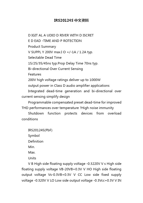
IRS20124S中文资料D IGIT AL A UDIO D RIVER WITH D ISCRETE D EAD -TIME AND P ROTECTIONProduct SummaryV SUPPL Y 200V max.I O +/-1A / 1.2A typ.Selectable Dead Time15/25/35/45ns typ.Prop Delay Time 70ns typ.Bi-directional Over Current SensingFeatures200V high voltage ratings deliver up to 1000Woutput power in Class D audio amplifier applicationsIntegrated dead-time generation and bi-directional over current sensing simplify designProgrammable compensated preset dead-time for improved THD performances over temperature ?High noise immunity Shutdown function protects devices from overload conditionsIRS20124S(PbF)SymbolDefinitionMin.Max.UnitsV B High side floating supply voltage -0.3220V V s High side floating supply voltage VB-20VB+0.3V V HO High side floating output voltage Vs-0.3VB+0.3V V CC Low side fixed supply voltage -0.320V V LO Low side output voltage -0.3Vcc+0.3V V INInput voltage-0.3Vcc+0.3V V OC OC pin input voltage-0.3Vcc+0.3V V OCSET1 OCSET1 pin input voltage -0.3Vcc+0.3V V OCSET2OCSET2 pin input voltage-0.3Vcc+0.3V dVs/dt Allowable Vs voltage slew rate-50V/ns Pd Maximum power dissipation- 1.25W Rth JA Thermal resistance, Junction to ambient -100°C/W T J Junctio n Temperature -150°C T S Storage Temperature-55150°CT LLead temperature (Soldering, 10 seconds)-300°CAbsolute Maximum RatingsAbsolute maximum ratings indicate sustained limits beyond which damage to the device may occur. All voltage parameters are absolute voltages referenced to COM. All currents are defined positive into any lead. The thermal resistance and power dissipation ratings are measured under board mounted and still air conditions.DescriptionThe IRS20124S is a high voltage, high speed power MOSFET driver with internal dead-time and shutdown functions specially designed for Class D audio amplifier applications.The internal dead time generation block provides accurate gate switch timing and enables tight dead-time settings for better THD performances.In order to maximize other audio performance characteristics,all switching times are designed for immunity from external disturbances such as VCC perturbation and incoming switching noise on the DT pin. Logic inputs are compatible with LSTTL output or standard CMOS down to 3.0V without speed degradation. The output drivers feature high current buffers capable of sourcing 1.0A and sinking 1.2A. Internal delays are optimized to achieve minimal dead-time variations. Proprietary HVIC and latch immune CMOS technologies guarantee operation down to Vs= –4V, providing outstanding capabilities of latch and surge immunities with rugged monolithic construction.Recommended Operating ConditionsFor Proper operation, the device should be used within the recommended conditions. The Vs and COM offset ratings are tested with all supplies biased at 15V differential.Symbol Definition Min.Max.Units V B High side floating supply absolute voltage Vs+10Vs+18V V S High side floating supply offset voltage Note 1200VV V HO High side floating output voltage Vs VB V CC Low side fixed supply voltage1018V V LO Low side output voltage0VCC V V IN Logic input voltage0VCC V V OC OC pin input voltage0VCC V V OCSET1OCSET1 pin input voltage0VCC V V OCSET2OCSET2 pin input voltage0VCC V T A Ambient Temperature-40125°CDynamic Electrical CharacteristicsV BIAS (V CC, V BS) = 15V, C L = 1nF and T A = 25°C unless otherwise specified. Figure 2 shows the timing definitions.IRS20124S(PbF)Lead DefinitionsSymbol DescriptionVCC Low side logic Supply voltage VB High side floating supply HO High side outputVS High side floating supply returnINLogic input for high and low side gate driver outputs (HO and LO), in phase with HODT/SD Input for programmable dead-time, referenced to COM. Shutdown LO and HO when tied to COM COM Low side supply returnLO Low side outputOC Over current output (negative logic)OC SET1Input for setting negative over current threshold OC SET2Input for setting positive over current thresholdIRS20124S(PbF)VBHOVSO O C S E T O C S E T VccLOCOM50%50%t off(L)t on(L)90%10%90%10%DT HO-LOt off(H)INHOLOt on(H)DT LO-HO DT/SDHO LOV SDT SD90%Figure 1. Switching Time Waveform Definitions Figure 2. Shutdown Waveform Definitions IRS20124S(PbF)toc filt HIGHVSOCV soct COMCOMtwocVSOCV Soc+tdocCOM COMLOV Soc-15V Vsoc+Vsoc-OCVsoc+Vsoc-COM VSOCFigure 5. OC Waveform DefinitionsFigure 3. OC Input FilterTime Definitions IRS20124S(PbF)IRS20124S(PbF)2.0()2()IRS20124S(PbF)2430()()IRS20124S(PbF)10()10()IRS20124S(PbF)。
PS5R-SE24中文资料
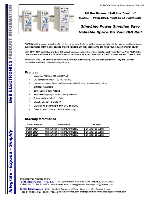
PS5R-Sx24 Slim-Line Power Supplies 0604 - 1/3a t e – E x p a n d – S i m p l i f yB &B E L EC T R O N I C S P R OD U C T I N F O R M A T I O NAll the Power, Half the Size! CEModels: PS5R-SC24, PS5R-SD24, PS5R-SE24Slim-Line Power Supplies Save Valuable Space On Your DIN RailPS5R Slim Line power supplies offer all the convenient features, all the power, at only half the size of traditional power supplies. Utilize them in tight spaces or save valuable DIN Rail space while still filling your requirements for power.With 30W, 60W and 90W and 24V DC output, you can choose the model that is exactly right for you. The PS5R Slim Line models are UL508 and UL1604 listed for hazardous locations. The 30W and 60W models are also Class 2 rated.The PS5R Slim Line series has worldwide approvals, fused inputs, and overload protection. They are DIN Rail mountable and have universal voltage inputs.Features• Universal AC input (85 to 264V AC) • DC compatible input (100 to 370V DC)• Unique spring-up, finger-safe terminals (ideal for ring lug terminated wire) • DIN Rail mountable • 30W, 60W, & 90W models• Auto resetting output overcurrent protection • Output voltage adjust (+/-10%) • UL508, UL1604, & UL1310• CE marking according to both LVD and EMC •Class 2 rated (30W and 60W models only)Ordering InformationModel NumberDescription OutputPS5R-SC24 Slim-Line DIN Rail Power Supply 24 VDC, 30 Watts PS5R-SD24 Slim-Line DIN Rail Power Supply 24 VDC, 60 Watts PS5R-SE24 Slim-Line DIN Rail Power Supply 24 VDC, 90 Watts元器件交易网PS5R-Sx24 Slim-Line Power Supplies 0604 - 2/3a t e – E x p a n d – S i m p l i f yB &B E L EC T R O N I C S P R OD U C T I N F O R M A T I O NSpecificationsModel Number:PS5R-SC24PS5R-SD24PS5R-SE24Wattage30W 60W90WInput Voltage(single-phase, 2-wire)85 to 264 VAC, 100 to 370 VDCInput Current (typical) 100VAC 200VAC0.9A 0.6A 1.7A 1.0A 2.3A 1.4A Internal Fuse Rating 3.15A 3.15A 4AInrush Current (cold start) 200VAC50A max. Leakage Current 0.75mA max.I n p u tTypical Efficiency 12VDC 24VDC78% 80% - 83% - 82%Output Current Ratings 12VDC 24VDC2.5A 1.3A - 2.5A -3.75AVoltage Adjustment ± 10% (V.ADJ control on front) Output Holding Time 20ms min. (at rated input and output) Rise Time100ms max. (at rated input and output)Line Regulation 0.4% max. Load Regulation1.5% max. Temperature Regulation 0.05% ºC max.Ripple Voltage2% peak-to-peak max.( including noise)Over-current Protection 105% or more, auto reset 103% to 110%, auto resetO u t p u t Over-voltage Protection 120% min. ShutdownDielectric Strength Between input and ground: 2000VAC, 1 minute(Between input and output: 3000VAC, 1 minute. Between output and ground: 500VAC, 1 minute)Insulation Resistance Between input and output terminals: 100M Ω min.Operating Temperature -10 to +60°C (14 to 140°F) Storage Temperature -25 to +75 °C (-13 to +167 °F)Operating Humidity 20 to 90% relative humidity (no condensation, no freezing)Vibration Resistance Frequency 10 to 55Hz, Amplitude 0.375mm Shock Resistance 300/ms 2 3 times each in 6 axes (150 m/s 2 using mounting bracket) ApprovalsEMC: EN61204-3 (EMI Class B, EMS: Industrial), LVD: EN60950,EN50178 listed, UL 1604, UL1310 (PS5R-SC. –SD), c-UL (CSA 22.2 No. 14)Harmonic Directive (EN61000-3-2) n/a n/a EN61000-3-2 A14 Class A Weight (approx.) grams ounces250 8.8 285 10.1 440 15.52Terminal Screw M3.5 slotted-Phillips head screw (screw terminal type)IP Protection IP20 (finger-safe)Dimensions HxWxDmm inches95 x 36 x 108 3.74 x 1.42 x 4.25 95 x 36 x 108 3.74 x 1.42 x 4.25 115 x 46 x 121 4.53 x 1.81 x 4.76元器件交易网PS5R-Sx24 Slim-Line Power Supplies 0604 - 3/3a t e – E x p a n d – S i m p l i f yB &B E L EC T R O N I C S P R OD U C T I N F O R M A T I O N元器件交易网。
LM124四运算放大器芯片的中文应用资料

四运算放大器芯片的中文应用资料LM124/LM224/LM324是四运放集成电路,它采用14管脚双列直插塑料(陶瓷)封装,外形如图所示。
它的内部包含四组形式完全相同的运算放大器,除电源共用外,四组运放相互独立。
每一组运算放大器可用图1所示的符号来表示,它有5个引出脚,其中“+”、“-”为两个信号输入端,“V+”、“V-”为正、负电源端,“Vo”为输出端。
两个信号输入端中,Vi-(-)为反相输入端,表示运放输出端Vo的信号与该输入端的相位相反;Vi+(+)为同相输入端,表示运放输出端Vo的信号与该输入端的相位相同。
LM124/LM224/LM324的引脚排列见图2。
图一图二lm324功能引脚图图3 LM324/LM124/LM224集成电路内部电路图1/4主要参数:参数名称测试条件最小典型最大单位输入失调电压U0≈1.4V RS=0 - 2.07.0mV输入失调电流 - - 5.050nA输入偏置电流 - -45250nA大信号电压增益U+=15V,R L=5kΩ 88k100k --电源电流U+=30V,U o=0,R L=∞ 1.5 3.0 -mA 共模抑制比R s≤10kΩ6570 -dB极限参数:LM124为陶瓷封装符号参数LM124 LM224 LM324 单位Vcc Supply Voltage 电源电压±16 or 32 V Vi Input Voltage 输入电压-0.3 to +32 VVid Differential InputVoltage -(*) 差分输入电压+32 +32 +32 VPtot PowerDissipation功耗后缀NSuffix500 500 500mW后缀DSuffix-400 400-Output Short-circuitDuration -(note 1)Infinite-Iin Input Current (note 6)输入电流50 50 50 mAToper Operating Free AirTemperature Range 工作温度-55 to+125-40 to+1050 to +70 ℃Tstg Storage TemperatureRange 储存温度范围-65 to+150-65 to+150-65 to+150℃由于LM124/LM224/LM324四运放电路具有电源电压范围宽,静态功耗小,可单电源使用,价格低廉等优点,因此被广泛应用在各种电路中。
SN74LVCH245APWLE中文资料
FEATURESSN74LVCH245A...RGY PACKAGE(TOP VIEW)I RB G NC CSN54LVCH245A...J OR W PACKAGE SN74LVCH245A...DB, DGV, DW, NS,OR PW PACKAGE(TOP VIEW)1234567891020191817161514131211DIR A1A2A3A4A5A6A7A8GNDV CC OE B1B2B3B4B5B6B7B8SN54LVCH245A...FK PACKAGE(TOP VIEW)3212019910111213456781817161514B1B2B3B4B5A3A4A5A6A7A 2A 1D I RB 7B 6O EA 8G N DB 8VC CDESCRIPTION/ORDERING INFORMATIONSN54LVCH245A,SN74LVCH245A OCTAL BUS TRANSCEIVERS WITH 3-STATE OUTPUTSSCES008O–JULY 1995–REVISED DECEMBER 2005•Operate From 1.65V to 3.6V •I off Supports Partial-Power-Down Mode Operation•Inputs Accept Voltages to 5.5V •Bus Hold on Data Inputs Eliminates the Need •Max t pd of 6.3ns at 3.3Vfor External Pullup/Pulldown Resistors•Typical V OLP (Output Ground Bounce)•Latch-Up Performance Exceeds 250mA Per <0.8V at V CC =3.3V,T A =25°CJESD 17•Typical V OHV (Output V OH Undershoot)•ESD Protection Exceeds JESD 22>2V at V CC =3.3V,T A =25°C–2000-V Human-Body Model (A114-A)•Support Mixed-Mode Signal Operation on All Ports (5-V Input/Output Voltage With –200-V Machine Model (A115-A)3.3-V V CC )The SN54LVCH245A octal bus transceiver is designed for 2.7-V to 3.6-V V CC operation,and the SN74LVCH245A octal bus transceiver is designed for 1.65-V to 3.6-V V CC operation.Inputs can be driven from either 3.3-V or 5-V devices.This feature allows the use of these devices as translators in a mixed 3.3-V/5-V system environment.These devices are designed for asynchronous communication between data buses.These devices transmit data from the A bus to the B bus or from the B bus to the A bus,depending on the logic level at the direction-control (DIR)input.The output-enable (OE)input can be used to disable the device so the buses are effectively isolated.These devices are fully specified for partial-power-down applications using I off .The I off circuitry disables the outputs,preventing damaging current backflow through the devices when they are powered down.To ensure the high-impedance state during power up or power down,OE should be tied to V CC through a pullup resistor;the minimum value of the resistor is determined by the current-sinking capability of the driver.Active bus-hold circuitry is provided to hold unused or floating data inputs at a valid logic e of pullup or pulldown resistors with the bus-hold circuitry is not recommended.The bus-hold circuitry is part of the input circuit and is not disabled by OE or DIR.Please be aware that an important notice concerning availability,standard warranty,and use in critical applications of Texas Instruments semiconductor products and disclaimers thereto appears at the end of this data sheet.GQN OR ZQN PACKAGE(TOP VIEW)1234A B C D ESN54LVCH245A,SN74LVCH245A OCTAL BUS TRANSCEIVERS WITH 3-STATE OUTPUTSSCES008O–JULY 1995–REVISED DECEMBER 2005ORDERING INFORMATIONT APACKAGE (1)ORDERABLE PART NUMBER TOP-SIDE MARKING QFN –RGY Reel of 1000SN74LVCH245ARGYR LCH245A Tube of 25SN74LVCH245ADW SOIC –DW LVCH245A Reel of 2000SN74LVCH245ADWR SOP –NS Reel of 2000SN74LVCH245ANSR LVCH245A SSOP –DBReel of 2000SN74LVCH245ADBR LCH245A–40°C to 85°CTube of 70SN74LVCH245APW TSSOP –PW Reel of 2000SN74LVCH245APWR LCH245AReel of 250SN74LVCH245APWT TVSOP –DGV Reel of 2000SN74LVCH245ADGVR LCH245A VFBGA –GQNSN74LVCH245AGQNR Reel of 1000LCH245AVFBGA –ZQN (Pb-free)SN74LVCH245AZQNR CDIP –JTube of 20SNJ54LVCH245AJ SNJ54LVCH245AJ –55°C to 125°CCFP –W Tube of 85SNJ54LVCH245AW SNJ54LVCH245AW LCCC –FKTube of 55SNJ54LVCH245AFKSNJ54LVCH245AFK (1)Package drawings,standard packing quantities,thermal data,symbolization,and PCB design guidelines are available at /sc/package.TERMINAL ASSIGNMENTS1234A A1DIR V CC OE B A3B2A2B1C A5A4B4B3D A7B6A6B5EGNDA8B8B7FUNCTION TABLEINPUTS OPERATION OE DIR L L B data to A bus L H A data to B busHXIsolationDIROEA1B1To Seven Other ChannelsAbsolute Maximum Ratings (1)SN54LVCH245A,SN74LVCH245A OCTAL BUS TRANSCEIVERS WITH 3-STATE OUTPUTSSCES008O–JULY 1995–REVISED DECEMBER 2005LOGIC DIAGRAM (POSITIVE LOGIC)over operating free-air temperature range (unless otherwise noted)MINMAX UNIT V CC Supply voltage range –0.5 6.5V V I Input voltage range (2)–0.5 6.5V V O Voltage range applied to any output in the high-impedance or power-off state (2)–0.5 6.5V V O Voltage range applied to any output in the high or low state (2)(3)–0.5V CC +0.5V I IK Input clamp current V I <0–50mA I OK Output clamp current V O <0–50mA I OContinuous output current±50mA Continuous current through V CC or GND±100mADB package (4)70DGV package (4)92DW package (4)58θJAPackage thermal impedanceGQN/ZQN package (4)78°C/W NS package (4)60PW package (4)83RGY package (5)37T stg Storage temperature range–65150°C (1)Stresses beyond those listed under "absolute maximum ratings"may cause permanent damage to the device.These are stress ratings only,and functional operation of the device at these or any other conditions beyond those indicated under "recommended operating conditions"is not implied.Exposure to absolute-maximum-rated conditions for extended periods may affect device reliability.(2)The input and output negative-voltage ratings may be exceeded if the input and output current ratings are observed.(3)The value of V CC is provided in the recommended operating conditions table.(4)The package thermal impedance is calculated in accordance with JESD 51-7.(5)The package thermal impedance is calculated in accordance with JESD 51-5.Recommended Operating Conditions (1)SN54LVCH245A,SN74LVCH245A OCTAL BUS TRANSCEIVERS WITH 3-STATE OUTPUTSSCES008O–JULY 1995–REVISED DECEMBER 2005SN54LVCH245A SN74LVCH245AUNIT MINMAX MIN MAX Operating2 3.61.65 3.6V CCSupply voltageVData retention only 1.51.5V CC =1.65V to 1.95V0.65×V CCV IHHigh-level input voltageV CC =2.3V to 2.7V 1.7VV CC =2.7V to 3.6V 22V CC =1.65V to 1.95V0.35×V CCV IL Low-level input voltage V CC =2.3V to 2.7V 0.7V V CC =2.7V to 3.6V0.80.8V I Input voltage 0 5.50 5.5V High or low state 0V CC 0V CC V OOutput voltageV 3-state 05.55.5V CC =1.65V–4V CC =2.3V –8I OHHigh-level output currentmA V CC =2.7V –12–12V CC =3V –24–24V CC =1.65V4V CC =2.3V 8I OLLow-level output currentmA V CC =2.7V 1212V CC =3V2424∆t/∆v Input transition rise or fall rate 1010ns/V T A Operating free-air temperature–55125–4085°C (1)All unused control inputs of the device must be held at V CC or GND to ensure proper device operation.Refer to the TI application report,Implications of Slow or Floating CMOS Inputs ,literature number SCBA004.Electrical CharacteristicsSN54LVCH245A,SN74LVCH245A OCTAL BUS TRANSCEIVERSWITH3-STATE OUTPUTS SCES008O–JULY1995–REVISED DECEMBER2005over recommended operating free-air temperature range(unless otherwise noted)SN54LVCH245A SN74LVCH245A PARAMETER TEST CONDITIONS V CC UNITMIN TYP(1)MAX MIN TYP(1)MAXV CC1.65V to3.6V–0.2I OH=–100µAV CC2.7V to3.6V–0.2I OH=–4mA 1.65V 1.2V OH VI OH=–8mA 2.3V 1.72.7V 2.2 2.2I OH=–12mA3V 2.4 2.4I OH=–24mA3V 2.2 2.21.65V to3.6V0.2I OL=100µA2.7V to3.6V0.2I OL=4mA 1.65V0.45V OL VI OL=8mA 2.3V0.7I OL=12mA 2.7V0.40.4I OL=24mA3V0.550.55I I Control inputs V I=0to5.5V 3.6V±5±5µAI off V I or V O=5.5V0±10µAV I=0.58V251.65VV I=1.07V–25V I=0.7V452.3VI I(hold)V I=1.7V–45µAV I=0.8V75753VV I=2V–75–75V I=0to3.6V(2) 3.6V±500±500I OZ(3)V O=0V or(V CC to5.5V) 2.3V to3.6V±15±5µAV I=V CC or GND1010I CC I O=0 3.6VµA3.6V≤V I≤5.5V(4)1010One input at V CC–0.6V,∆I CC 2.7V to3.6V500500µA Other inputs at V CC or GNDC i Control inputs V I=V CC or GND 3.3V4124pFC io A or B port V O=V CC or GND 3.3V 5.512 5.5pF(1)All typical values are at V CC=3.3V,T A=25°C.(2)This is the bus-hold maximum dynamic current required to switch the input from one state to another.(3)For the total leakage current in an I/O port,please consult the I I(hold)specification for the input voltage condition0V<V I<V CC,and theI OZ specification for the input voltage conditions V I=0V or V I=V CC to5.5V.The bus-hold current,at input voltage greater than V CC,isnegligible.(4)This applies in the disabled state only.Switching CharacteristicsSwitching CharacteristicsOperating CharacteristicsSN54LVCH245A,SN74LVCH245A OCTAL BUS TRANSCEIVERS WITH 3-STATE OUTPUTSSCES008O–JULY 1995–REVISED DECEMBER 2005over recommended operating free-air temperature range (unless otherwise noted)(see Figure 1)SN54LVCH245AFROM TO V CC =3.3V PARAMETERV CC =2.7V UNIT(INPUT)(OUTPUT)±0.3V MIN MAXMIN MAXt pd A or B B or A 817ns t en OE A or B 9.518.5ns t disOEA or B8.517.5ns over recommended operating free-air temperature range (unless otherwise noted)(see Figure 1)SN74LVCH245AFROM TO V CC =1.8V V CC =2.5V V CC =3.3V PARAMETERV CC =2.7V UNIT(INPUT)(OUTPUT)±0.15V ±0.2V ±0.3V MINMAXMINMAXMINMAX MIN MAX t pd A or B B or A (1)(1)(1)(1)7.3 1.5 6.3ns t en OE A or B (1)(1)(1)(1)9.5 1.58.5ns t dis OEA or B(1)(1)(1)(1)8.51.77.5ns t sk(o)1ns(1)This information was not available at the time of publication.T A =25°CV CC =1.8VV CC =2.5VV CC =3.3VTEST PARAMETERUNIT CONDITIONS TYPTYPTYP Outputs enabled (1)(1)47Power dissipation capacitance C pd f =10MHzpFper transceiverOutputs disabled(1)(1)2(1)This information was not available at the time of publication.PARAMETER MEASUREMENT INFORMATIONFrom Output Under TestLOAD CIRCUITOpen Data InputTiming InputV I0 VV I0 V0 VInputVOLTAGE WAVEFORMS SETUP AND HOLD TIMESVOLTAGE WAVEFORMS PROPAGATION DELAY TIMESINVERTING AND NONINVERTING OUTPUTSVOLTAGE WAVEFORMS PULSE DURATIONV OHV OHV OLV OLV I0 V InputOutput Waveform 1S1 at V LOAD (see Note B)Output Waveform 2S1 at GND (see Note B)V OLV OH V LOAD /20 V≈0 VV IVOLTAGE WAVEFORMS ENABLE AND DISABLE TIMES LOW- AND HIGH-LEVEL ENABLINGOutputOutputt PLH /t PHL t PLZ /t PZL t PHZ /t PZHOpen V LOAD GNDTEST S1NOTES: A.C L includes probe and jig capacitance.B.Waveform 1 is for an output with internal conditions such that the output is low, except when disabled by the output control.Waveform 2 is for an output with internal conditions such that the output is high, except when disabled by the output control.C.All input pulses are supplied by generators having the following characteristics: PRR ≤ 10 MHz, Z O = 50 Ω.D.The outputs are measured one at a time with, one transition per measurement.E.t PLZ and t PHZ are the same as t dis .F.t PZL and t PZH are the same as t en .G.t PLH and t PHL are the same as t pd .H.All parameters and waveforms are not applicable to all devices.Output Control V I1.8 V ± 0.15 V2.5 V ± 0.2 V2.7 V3.3 V ± 0.3 V1 k Ω500 Ω500 Ω500 ΩV CC R L 2 × V CC 2 × V CC 6 V 6 VV LOAD C L 30 pF 30 pF 50 pF 50 pF0.15 V 0.15 V 0.3 V 0.3 VV ∆V CC V CC 2.7 V 2.7 VV I V CC /2V CC /21.5 V 1.5 VV M t r /t f ≤2 ns ≤2 ns ≤2.5 ns ≤2.5 nsINPUTS SN54LVCH245A,SN74LVCH245A OCTAL BUS TRANSCEIVERS WITH 3-STATE OUTPUTSSCES008O–JULY 1995–REVISED DECEMBER 2005Figure 1.Load Circuit and Voltage WaveformsPACKAGING INFORMATIONOrderableDevice Status (1)Package Type Package Drawing Pins Package Qty Eco Plan (2)Lead/Ball FinishMSL Peak Temp (3)5962-9754301Q2A ACTIVE LCCC FK 201TBD POST-PLATE N /A for Pkg Type 5962-9754301QRA ACTIVE CDIP J 201TBD A42SNPB N /A for Pkg Type 5962-9754301QSA ACTIVE CFP W 201TBD A42N /A for Pkg Type 5962-9754301V2A ACTIVE LCCC FK 201TBD POST-PLATE N /A for Pkg Type5962-9754301VRA ACTIVE CDIP J 201TBD A42SNPB N /A for Pkg Type 5962-9754301VSA ACTIVE CFP W 201TBD A42N /A for Pkg Type SN74LVCH245ADBLE OBSOLETE SSOP DB 20TBDCall TI Call TISN74LVCH245ADBR ACTIVE SSOP DB 202000Green (RoHS &no Sb/Br)CU NIPDAU Level-1-260C-UNLIM SN74LVCH245ADBRE4ACTIVE SSOP DB 202000Green (RoHS &no Sb/Br)CU NIPDAU Level-1-260C-UNLIM SN74LVCH245ADBRG4ACTIVE SSOP DB 202000Green (RoHS &no Sb/Br)CU NIPDAU Level-1-260C-UNLIM SN74LVCH245ADGVR ACTIVE TVSOP DGV 202000Green (RoHS &no Sb/Br)CU NIPDAU Level-1-260C-UNLIM SN74LVCH245ADGVRE4ACTIVE TVSOP DGV 202000Green (RoHS &no Sb/Br)CU NIPDAU Level-1-260C-UNLIM SN74LVCH245ADGVRG4ACTIVE TVSOP DGV 202000Green (RoHS &no Sb/Br)CU NIPDAU Level-1-260C-UNLIM SN74LVCH245ADW ACTIVE SOIC DW 2025Green (RoHS &no Sb/Br)CU NIPDAU Level-1-260C-UNLIM SN74LVCH245ADWE4ACTIVE SOIC DW 2025Green (RoHS &no Sb/Br)CU NIPDAU Level-1-260C-UNLIM SN74LVCH245ADWG4ACTIVE SOIC DW 2025Green (RoHS &no Sb/Br)CU NIPDAU Level-1-260C-UNLIM SN74LVCH245ADWR ACTIVE SOIC DW 202000Green (RoHS &no Sb/Br)CU NIPDAU Level-1-260C-UNLIM SN74LVCH245ADWRE4ACTIVE SOIC DW 202000Green (RoHS &no Sb/Br)CU NIPDAU Level-1-260C-UNLIM SN74LVCH245ADWRG4ACTIVE SOIC DW 202000Green (RoHS &no Sb/Br)CU NIPDAU Level-1-260C-UNLIM SN74LVCH245AGQNRNRNDBGA MI CROSTA R JUNI ORGQN201000TBDSNPBLevel-1-240C-UNLIMSN74LVCH245ANSR ACTIVE SO NS 202000Green (RoHS &no Sb/Br)CU NIPDAU Level-1-260C-UNLIM SN74LVCH245ANSRE4ACTIVE SO NS 202000Green (RoHS &no Sb/Br)CU NIPDAU Level-1-260C-UNLIM SN74LVCH245ANSRG4ACTIVE SO NS 202000Green (RoHS &no Sb/Br)CU NIPDAU Level-1-260C-UNLIM SN74LVCH245APW ACTIVE TSSOP PW 2070Green (RoHS &no Sb/Br)CU NIPDAU Level-1-260C-UNLIM SN74LVCH245APWE4ACTIVE TSSOP PW 2070Green (RoHS &no Sb/Br)CU NIPDAU Level-1-260C-UNLIM SN74LVCH245APWG4ACTIVE TSSOP PW 2070Green (RoHS &no Sb/Br)CU NIPDAU Level-1-260C-UNLIM SN74LVCH245APWLEOBSOLETETSSOPPW20TBDCall TICall TI3-Jan-2008Orderable Device Status(1)PackageType PackageDrawingPins PackageQtyEco Plan(2)Lead/Ball Finish MSL Peak Temp(3)SN74LVCH245APWR ACTIVE TSSOP PW202000Green(RoHS&no Sb/Br)CU NIPDAU Level-1-260C-UNLIMSN74LVCH245APWRE4ACTIVE TSSOP PW202000Green(RoHS&no Sb/Br)CU NIPDAU Level-1-260C-UNLIMSN74LVCH245APWRG4ACTIVE TSSOP PW202000Green(RoHS&no Sb/Br)CU NIPDAU Level-1-260C-UNLIMSN74LVCH245APWT ACTIVE TSSOP PW20250Green(RoHS&no Sb/Br)CU NIPDAU Level-1-260C-UNLIMSN74LVCH245APWTE4ACTIVE TSSOP PW20250Green(RoHS&no Sb/Br)CU NIPDAU Level-1-260C-UNLIMSN74LVCH245APWTG4ACTIVE TSSOP PW20250Green(RoHS&no Sb/Br)CU NIPDAU Level-1-260C-UNLIMSN74LVCH245ARGYR ACTIVE QFN RGY201000Green(RoHS&no Sb/Br)CU NIPDAU Level-2-260C-1YEARSN74LVCH245ARGYRG4ACTIVE QFN RGY201000Green(RoHS&no Sb/Br)CU NIPDAU Level-2-260C-1YEARSN74LVCH245AZQNR ACTIVE BGA MICROSTAR JUNIOR ZQN201000Green(RoHS&no Sb/Br)SNAGCU Level-1-260C-UNLIMSN74LVCH245AZXYR ACTIVE BGA MICROSTAR JUNIOR ZXY202500Green(RoHS&no Sb/Br)SNAGCU Level-1-260C-UNLIMSNJ54LVCH245AFK ACTIVE LCCC FK201TBD POST-PLATE N/A for Pkg Type SNJ54LVCH245AJ ACTIVE CDIP J201TBD A42SNPB N/A for Pkg Type SNJ54LVCH245AW ACTIVE CFP W201TBD A42N/A for Pkg Type(1)The marketing status values are defined as follows:ACTIVE:Product device recommended for new designs.LIFEBUY:TI has announced that the device will be discontinued,and a lifetime-buy period is in effect.NRND:Not recommended for new designs.Device is in production to support existing customers,but TI does not recommend using this part ina new design.PREVIEW:Device has been announced but is not in production.Samples may or may not be available.OBSOLETE:TI has discontinued the production of the device.(2)Eco Plan-The planned eco-friendly classification:Pb-Free(RoHS),Pb-Free(RoHS Exempt),or Green(RoHS&no Sb/Br)-please check /productcontent for the latest availability information and additional product content details.TBD:The Pb-Free/Green conversion plan has not been defined.Pb-Free(RoHS):TI's terms"Lead-Free"or"Pb-Free"mean semiconductor products that are compatible with the current RoHS requirements for all6substances,including the requirement that lead not exceed0.1%by weight in homogeneous materials.Where designed to be soldered at high temperatures,TI Pb-Free products are suitable for use in specified lead-free processes.Pb-Free(RoHS Exempt):This component has a RoHS exemption for either1)lead-based flip-chip solder bumps used between the die and package,or2)lead-based die adhesive used between the die and leadframe.The component is otherwise considered Pb-Free(RoHS compatible)as defined above.Green(RoHS&no Sb/Br):TI defines"Green"to mean Pb-Free(RoHS compatible),and free of Bromine(Br)and Antimony(Sb)based flame retardants(Br or Sb do not exceed0.1%by weight in homogeneous material)(3)MSL,Peak Temp.--The Moisture Sensitivity Level rating according to the JEDEC industry standard classifications,and peak solder temperature.Important Information and Disclaimer:The information provided on this page represents TI's knowledge and belief as of the date that it is provided.TI bases its knowledge and belief on information provided by third parties,and makes no representation or warranty as to the accuracy of such information.Efforts are underway to better integrate information from third parties.TI has taken and continues to take reasonable steps to provide representative and accurate information but may not have conducted destructive testing or chemical analysis on incoming materials and chemicals.TI and TI suppliers consider certain information to be proprietary,and thus CAS numbers and other limited 3-Jan-2008information may not be available for release.In no event shall TI's liability arising out of such information exceed the total purchase price of the TI part(s)at issue in this document sold by TI to Customer on an annualbasis.3-Jan-2008TAPE AND REEL BOXINFORMATIONDevicePackage Pins SiteReel Diameter (mm)Reel Width (mm)A0(mm)B0(mm)K0(mm)P1(mm)W (mm)Pin1Quadrant SN74LVCH245ADBR DB 20SITE 41330168.27.5 2.51216Q1SN74LVCH245ADGVR DGV 20SITE 41330127.0 5.6 1.6812Q1SN74LVCH245ADWR DW 20SITE 413302410.813.0 2.71224Q1SN74LVCH245AGQNR GQN 20SITE 3233012 3.3 4.3 1.5812Q1SN74LVCH245AGQNR GQN 20SITE 6033012 3.3 4.3 1.6812Q1SN74LVCH245APWR PW 20SITE 4133016 6.957.1 1.6816Q1SN74LVCH245ARGYR RGY 20SITE 4118012 3.8 4.8 1.6812Q1SN74LVCH245AZQNR ZQN 20SITE 3233012 3.3 4.3 1.5812Q1SN74LVCH245AZQNR ZQN 20SITE 6033012 3.3 4.3 1.6812Q1SN74LVCH245AZXYRZXY20SITE 60330122.83.31.0412Q212-Jan-2008DevicePackage Pins Site Length (mm)Width (mm)Height (mm)SN74LVCH245ADBR DB 20SITE 41346.0346.033.0SN74LVCH245ADGVR DGV 20SITE 41346.0346.029.0SN74LVCH245ADWR DW 20SITE 41346.0346.041.0SN74LVCH245AGQNR GQN 20SITE 32346.0346.029.0SN74LVCH245AGQNR GQN 20SITE 60342.9338.120.64SN74LVCH245APWR PW 20SITE 41346.0346.033.0SN74LVCH245ARGYR RGY 20SITE 41190.5212.731.75SN74LVCH245AZQNR ZQN 20SITE 32346.0346.029.0SN74LVCH245AZQNR ZQN 20SITE 60342.9338.120.64SN74LVCH245AZXYRZXY20SITE 60342.9338.120.6412-Jan-2008IMPORTANT NOTICETexas Instruments Incorporated and its subsidiaries(TI)reserve the right to make corrections,modifications,enhancements,improvements, and other changes to its products and services at any time and to discontinue any product or service without notice.Customers should obtain the latest relevant information before placing orders and should verify that such information is current and complete.All products are sold subject to TI’s terms and conditions of sale supplied at the time of order acknowledgment.TI warrants performance of its hardware products to the specifications applicable at the time of sale in accordance with TI’s standard warranty.Testing and other quality control techniques are used to the extent TI deems necessary to support this warranty.Except where mandated by government requirements,testing of all parameters of each product is not necessarily performed.TI assumes no liability for applications assistance or customer product design.Customers are responsible for their products and applications using TI components.To minimize the risks associated with customer products and applications,customers should provide adequate design and operating safeguards.TI does not warrant or represent that any license,either express or implied,is granted under any TI patent right,copyright,mask work right, or other TI intellectual property right relating to any combination,machine,or process in which TI products or services are rmation published by TI regarding third-party products or services does not constitute a license from TI to use such products or services or a warranty or endorsement e of such information may require a license from a third party under the patents or other intellectual property of the third party,or a license from TI under the patents or other intellectual property of TI.Reproduction of TI information in TI data books or data sheets is permissible only if reproduction is without alteration and is accompanied by all associated warranties,conditions,limitations,and notices.Reproduction of this information with alteration is an unfair and deceptive business practice.TI is not responsible or liable for such altered rmation of third parties may be subject to additional restrictions.Resale of TI products or services with statements different from or beyond the parameters stated by TI for that product or service voids all express and any implied warranties for the associated TI product or service and is an unfair and deceptive business practice.TI is not responsible or liable for any such statements.TI products are not authorized for use in safety-critical applications(such as life support)where a failure of the TI product would reasonably be expected to cause severe personal injury or death,unless officers of the parties have executed an agreement specifically governing such use.Buyers represent that they have all necessary expertise in the safety and regulatory ramifications of their applications,and acknowledge and agree that they are solely responsible for all legal,regulatory and safety-related requirements concerning their products and any use of TI products in such safety-critical applications,notwithstanding any applications-related information or support that may be provided by TI.Further,Buyers must fully indemnify TI and its representatives against any damages arising out of the use of TI products in such safety-critical applications.TI products are neither designed nor intended for use in military/aerospace applications or environments unless the TI products are specifically designated by TI as military-grade or"enhanced plastic."Only products designated by TI as military-grade meet military specifications.Buyers acknowledge and agree that any such use of TI products which TI has not designated as military-grade is solely at the Buyer's risk,and that they are solely responsible for compliance with all legal and regulatory requirements in connection with such use. TI products are neither designed nor intended for use in automotive applications or environments unless the specific TI products are designated by TI as compliant with ISO/TS16949requirements.Buyers acknowledge and agree that,if they use any non-designated products in automotive applications,TI will not be responsible for any failure to meet such requirements.Following are URLs where you can obtain information on other Texas Instruments products and application solutions:Products ApplicationsAmplifiers Audio /audioData Converters Automotive /automotiveDSP Broadband /broadbandClocks and Timers /clocks Digital Control /digitalcontrolInterface Medical /medicalLogic Military /militaryPower Mgmt Optical Networking /opticalnetwork Microcontrollers Security /securityRFID Telephony /telephonyRF/IF and ZigBee®Solutions /lprf Video&Imaging /videoWireless /wirelessMailing Address:Texas Instruments,Post Office Box655303,Dallas,Texas75265Copyright2008,Texas Instruments Incorporated。
NTE5444资料
NTE5442 thru NTE5448Silicon Controlled Rectifier (SCR)8 AmpDescription:The NTE5442 thru NTE5448 are silicon controlled rectifiers (SCR’s) in a TO127 type package de-signed for high–volume consumer phase–control applications such as motor speed, temperature, and light controls, and for fast switching applications in ignition and starting systems, voltage regula-tors, vending machines, and lamp drivers.Features:D Small, Rugged ConstructionD Practical Level Triggering and Holding Characteristics @ +25°C:I GT = 7mA TypI Hold = 6mA TypD Low “ON” Voltage: V TM = 1V Typ @ 5A @ +25°CD High Surge Current Rating: I TSM = 80AAbsolute Maximum Ratings: (Note 1, T J = +100°C unless otherwise specified)Peak Repetitive Forward and Reverse Blocking Voltage (Note 2), V DRM or V RRM. . . . . . . . . . . . . . . . . . . . . . . . . . . . . . . . . . . . . . . . . . . . . . . . . . . . . . . . . . . . . . . . . . . .NTE544250V . . . . . . . . . . . . . . . . . . . . . . . . . . . . . . . . . . . . . . . . . . . . . . . . . . . . . . . . . . . . . . . . . . .NTE5444200V . . . . . . . . . . . . . . . . . . . . . . . . . . . . . . . . . . . . . . . . . . . . . . . . . . . . . . . . . . . . . . . . . . .NTE5446400V . . . . . . . . . . . . . . . . . . . . . . . . . . . . . . . . . . . . . . . . . . . . . . . . . . . . . . . . . . . . . . . . . . .NTE5448600V Non–Repetitive Peak Reverse Blocking Voltage (t = 5ms (max) duration), V RSMNTE544275V . . . . . . . . . . . . . . . . . . . . . . . . . . . . . . . . . . . . . . . . . . . . . . . . . . . . . . . . . . . . . . . . . . . .. . . . . . . . . . . . . . . . . . . . . . . . . . . . . . . . . . . . . . . . . . . . . . . . . . . . . . . . . . . . . . . . . . .NTE5444300V . . . . . . . . . . . . . . . . . . . . . . . . . . . . . . . . . . . . . . . . . . . . . . . . . . . . . . . . . . . . . . . . . . .NTE5446500V . . . . . . . . . . . . . . . . . . . . . . . . . . . . . . . . . . . . . . . . . . . . . . . . . . . . . . . . . . . . . . . . . . .NTE5448700V. . . . . . . . . . . . . . . . . . . . . . . . . . . . . . . . . . RMS On–State Current (All Conduction Angles), I T(RMS)8A. . . . . . . . . . . . . . . . . . . . . . . . . . . . . . . . . . . . . . . Average On–State Current (T C = +73°C), I T(AV) 5.1A Peak Non–Repetitive Surge Current, I TSM. . . . . . . . . . . . .(1/2 cycle, 60Hz preceeded and followed by rated current and voltage)80A. . . . . . . . . . . . . . . . . . . . . . . . . . .Circuit Fusing (T J = –40° to +100°C, t = 1ms to 8.3ms), I2t25A2sec. . . . . . . . . . . . . . . . . . . . . . . . . . . . . . . . . . . . . . . . . . . . . . . . . . . . . . . . . . . . . Peak Gate Power, P GM5W. . . . . . . . . . . . . . . . . . . . . . . . . . . . . . . . . . . . . . . . . . . . . . . . . . . . . . Average Gate Power, P G(AV)500mW. . . . . . . . . . . . . . . . . . . . . . . . . . . . . . . . . . . . . . . . . . . . . . . . . . . . . . Peak Forward Gate Current, I GM2A Peak Reverse Gate Voltage, V RGM10V. . . . . . . . . . . . . . . . . . . . . . . . . . . . . . . . . . . . . . . . . . . . . . . . . . .. . . . . . . . . . . . . . . . . . . . . . . . . . . . . . . . . .Operating Junction Temperature Range, T J–40° to +100°C. . . . . . . . . . . . . . . . . . . . . . . . . . . . . . . . . . . . . . . . . .Storage Temperature Range, T stg–40° to +150°C. . . . . . . . . . . . . . . . . . . . . . . . . . . . Maximum Thermal Resistance, Junction–to–Case, R thJC 2.5°C/W. . . . . . . . . . . . . . . . . . . . . . . . . . . . . Typical Thermal Resistance, Junction–to–Ambient, R thJA40°C/W Note 1.NTE5444 and NTE5446 are discontinued devices and are replaced by NTE5448.Note 2.Ratings apply for zero or negative gate voltage but positive gate voltage shall not be applied concurrently with a negative potential on the anode. When checking forward or reverse blocking capability, thyristor devices should not be tested with a constant current source ina manner that the voltage applied exceeds the rated blocking voltage.Electrical Characteristics: (T= +25°C unless otherwise specified)。
LTV354T-A中文资料
LTV354T-A中⽂资料FEATURES* AC input response* Current transfer ratio( CTR : MIN. 20% at I F =±1mA, V CE =5V )* Isolation voltage between input and output LTV-354T( V iso =3,750Vrms )* Employs double transfer mold technology* Subminiature type( The volume is smaller than that of conventional DIP type by as far as 30% ) * Mini-flat package : 2.0 profile : LTV-354T* UL approved ( No. E113898 )* CUL approved ( No. E113898 , 01SC19287 )* CSA approved ( No. 1243207 )* FIMKO approved ( No. FI-16420 )* NEMKO approved ( No. P0******* )* DEMKO approved ( No. 310475-01 )* SEMKO approved ( No. 0109173 / 01-08 )* VDE approved ( No. 094722 )* RoHS complianceAPPLICATIONS* Hybrid substrates that require high density mounting.* Programmable controllersOUTLINE DIMENSIONSLTV-354T :*1. 2-digit date code.*2. Factory identification mark shall be marked (Z : Taiwan, Y : Thailand, X : China). *3. Rank shall be or shall not be marked.ABSOLUTE MAXIMUM RATING( Ta = 25°C ) PARAMETER SYMBOL RATING UNIT Forward Current I F±50 mA INPUTPower Dissipation P 70 mWCollector - Emitter Voltage V CEO35 VEmitter - Collector Voltage V ECO 6 V OUTPUT Collector Current I C50 mACollector Power Dissipation P C150 mW Total Power Dissipation P tot170 mW*1 Isolation Voltage V iso3,750 Vrms Operating Temperature T opr-55 ~ +100 °C Storage Temperature T stg-55 ~ +150 °C*2 Soldering Temperature T sol260 °C*1. AC For 1 Minute, R.H. = 40 ~ 60%Isolation voltage shall be measured using the following method.(1) Short between anode and cathode on the primary side and between collector and emitter on the secondary side.(2) The isolation voltage tester with zero-cross circuit shall be used.(3) The waveform of applied voltage shall be a sine wave.*2. For 10 SecondsRANK TABLE OF CURRENT TRANSFER RATIO CTR MODEL NO. RANK MARK CTR ( % )A 50 ~ 150LTV-354TA or No mark 20 ~ 400CONDITIONS I F = ±1 mA V CE = 5 V Ta = 25 °CTEMPERATURE PROFILE OF SOLDERING REFLOW(1)One time soldering reflow is recommended within the condition of temperature and time profile shown below.。
单片机技术应用
单片机如下的发展趋势:低功耗CMOS化、微型单片化、主流与多品种共存、功能更强大。
8051芯片内部共有256个字节单、RAM存储器和4KB字节单元的ROM存储器、其中RAM 存储器又分为高128字节单元和低128个字节单元。
而高128个存储单元中的一部分被特殊功能寄存器占用,其余单元用户不能使用。
通常所说的内RAM ,就是指低128个字节单元。
而rom存储器主要用于存放程序、原始数据和表格内容,成为程序存储器,也成为片内ROM。
8051芯片内部有一个高增益反向放大器,用于构成震荡电路。
反相放大器的输入端和输出端用于外接石英晶体和微调电容构成震荡电路。
始终周期:时钟周期又称为震荡周期。
状态周期:一个状态周期等于两个时钟周期。
机器周期:1个机器周期等于6个状态周期(12震荡周期)指令周期:指令周期是指执行一条指令所需要的时间,一个指令周期又1~4个机器周期组成。
单片机每一个指令的执行都可以包括取指和执行两个过程。
CPU执行指令时,由程序储存器中读取指令代码送入指令寄存器,经译码后由定时与控制电路发出相应的控制信号,完成指令功能。
MCS-51单片机共有4个8位的准双向并行I/O端口,即P0、P1、P2、P3,这些端口既可以作为一般的输入输出口使用,也还可以用作他用。
8051单片机共有5个中断源,即2个外部中断源、两个定时器/计数器、1个串行口中断源。
全部中断源可以设定为高低2个优先级,用来满足控制应用的需要。
RST是复位信号输入端,高电平有效。
系统通电后在此引脚上至少要保持2个机器周期(24个时钟周期)以上的高电平才能有效地完成复位操作。
PSEN:该引脚的功能主要用于片外ROM读选通信号输出端。
EA为片内、外ROM选择控制引脚,当=1(接高电平)时,表示方位片内ROM;=0(接地)时,表示访问片外ROM。
MCS-51单片机低12B的数据存储器RAM,按其功能的不同,可划分为三个区域。
工作寄存器区分为4组,一次被称为第0~3组,每组都可以用R0~R7作为单元编号。
- 1、下载文档前请自行甄别文档内容的完整性,平台不提供额外的编辑、内容补充、找答案等附加服务。
- 2、"仅部分预览"的文档,不可在线预览部分如存在完整性等问题,可反馈申请退款(可完整预览的文档不适用该条件!)。
- 3、如文档侵犯您的权益,请联系客服反馈,我们会尽快为您处理(人工客服工作时间:9:00-18:30)。
EC 42
August 2002
元器件交易网
ECONOLINE - DC/DC-Converter
RXT & RYT Series, 1W, DIP14, Regulated, Isolated Outputs (Dual Output) Package Style and Pinning (mm)
● ● ● ●
No Heatsink Required Toroidal Magnetics No Extern. Components Required Input/Output Isolation 1kVDC
Selection Guide
Part Number DIP 14 RXT-XX0505 RXT-XX0909 RXT-XX1212 RXT-XX1515 RXT-XX0524 Part Number SIP 7 RYT-XX0505 RYT-XX0909 RYT-XX1212 RYT-XX1515 RYT-XX0524 Input Voltage (VDC) 5, 9, 12, 15, 24 5, 9, 12, 15, 24 5, 9, 12, 15, 24 5, 9, 12, 15, 24 5, 9, 12, 15, 24 Output Voltage (V1VDC) 5 9 12 15 24 Output Voltage (V2VDC) 5 9 12 15 24 Ouput Current (mA) 100/100 55/55 42/42 33/33 21/21 Efficiency (%) 53 58 62 65 65
元器件交易网
ECONOLINE - DC/DC-Converter
RXT & RYT Series, 1W, DIP14, Regulated, Isolated Outputs (Dual Output) Features
● ● ● ●
Isolated Outputs
Output/Output Isolation 1kVDC Power Sharing on Outputs UL 94V-0 Package Material
August 2002
EC 43
Output Power (Watts) 1.5 1.0 Safe Operating Area 0,5 0 -25 0 50 100 125 150 70 Operating Temperature ˚C 2.0
50% min. 1.000VDC min. 10 GΩ min. 40pF min./72pF max. 1.000VDC min. 1 Second 38kHz min. / 85kHz max. -25°C to +70°C (see Graph) -55°C to +125°C 2.9g
2.54
Pin Connections RXT Pin # 1 6 7 8 9 14 Dual –Vin +Vout 1 –Vout 1 –Vout 2 +Vout 2 +Vin
Pin Connections RYT Pin # 1 2 4 5 6 7 Dual +Vin –Vout +Vout 1 –Vout 1 +Vout 2 –Vout 2 XX.X ± 0.5 mm XX.XX ± 0.typ.
1 2 4 5 6 7
7.10 1.27 2.0
1 2 4 5 6 7
0.25
15.24 2.0
3.05
15.24
Recommended Footprint Details
1.00 ø+0.15/–0 1.00 ø+0.15/–0 2.54 2.54
2.54
14 PIN DIP Package 7 PIN SIP Package
d angle ojection
1 Bottom View
6 7
19.65 7.05
14
9 8
19.90 10.20
RXT-050505 RECOM **** RYT-051212 RECOM ****
0.51 typ.
RYT-051212 RECOM ****
Specifications (Core Operating Area) and Operating Temperature / Derating-Graph
Input Voltage Input Filter Output Voltage Accuracy Line Voltage Regulation Load Voltage Regulation (20% to 100% full load) Ripple and Noise (20MHz limited) Efficiency at Full Load Isolation Voltage Isolation Resistance (Viso = 500VDC) Isolation Capacitance Outputs Isolation Voltage Short Circuit Protection Switching Frequency at Full Load Operating Temperature Storage Temperature Package Weight ±5% Capacitor Type ±5% ±0.5% - ±1% ±0.5% - ±1.0% 100mV p-p max.