321632中文资料
2532中文资料

SWITCH-MODE TRANSFORMER GUIDE BY TECHNOLOGY
Ferrite
E30/15/7 ETD29X16X10 ETD29X15X10 ETD29X11X10 ETD34X13X11 ETD34X17X11 ETD39X17X13 ER48X18X18 ER54X20X18
This transformer is mainly intended to be used as a Resonant Switch-Mode Transformer for high-end 30” to 42” LCD TV sets with mains insulation. The most suitable circuit topology for this transformer is a half-bridge, quasi-resonant converter using ON Semiconductor’s ZVS controller MC34067. The common range of operation for this Switch-Mode Transformer is from 50-150 kHz.
9+9 6+6 6+6 8+8 7+7 9+9 9+9 7+7 11 +11 6+6 6+6
6+6
4+4 6+6 9+9 4+4 5+4 4+4 4+4 5+5 5+5 5+5 5+5 5+5 7+7
Slot Slot Slot Slot Slot Slot Slot Slot Slot Slot
32162丙烯腈
32162丙烯腈(抑制了的)第一部分化学品标识中文名: 丙烯腈(抑制了的); 乙烯基氰英文名: acrylonitrile; cyanoethylene第二部分成分/组成信息主要成分: 含量: 一级≥99%;二级98%。
CAS 号: 107-13-1相对分子质量: 53.06分子式: C3H3N化学类别: 丙烯酰基化合物第三部分危险性概述危险性类别: 第3.2类中闪点易燃液体危险性综述: 本品易燃,高毒,为可疑致癌物,对环境有严重危害,对水体可造成污染。
侵入途径: 吸入、食入、经皮吸收。
健康危害: 本品在体内析出氰根,抑制呼吸酶;对呼吸中枢有直接麻醉作用。
急性中毒表现与氢氰酸相似。
急性中毒:以中枢神经系统症状为主,伴有上呼吸道和眼部刺激症状。
轻度中毒有头晕、头痛、乏力、上腹部不适、恶心、呕吐、胸闷、手足麻木、意识蒙胧及口唇紫绀等。
眼结膜及鼻、咽部充血。
重者除上述症状加重外,出现四肢阵发性强直抽搐、昏迷。
液体污染皮肤,可致皮炎,局部出现红斑、丘疹或水疱。
慢性中毒:尚无定论。
长期接触,部分工人出现神衰综合征,低血压等。
对肝脏影响未肯定。
第四部分急救措施皮肤接触: 立即脱去污染的衣着,用流动清水或5%硫代硫酸钠溶液彻底冲洗至少20分钟。
就医。
眼睛接触: 提起眼睑,用流动清水或生理盐水冲洗。
就医。
吸入: 迅速脱离现场至空气新鲜处。
保持呼吸道通畅。
如呼吸困难,给输氧。
呼吸心跳停止时,立即进行人工呼吸(勿用口对口)和胸外心脏按压术。
给吸入亚硝酸异戊酯,就医。
食入: 饮足量温水,催吐。
洗胃。
用1:5000高锰酸钾或5%硫代硫酸钠溶液洗胃。
就医。
第五部分消防措施燃烧性: 易燃闪点(℃): -5 引燃温度(℃): 480爆炸下限[%(V/V)]: 2.8 爆炸上限[%(V/V)]: 28.0最小点火能(mJ): 0.16 最大爆炸压力(MPa): 无资料危险特性: 易燃,其蒸气与空气可形成爆炸性混合物。
遇明火、高热易引起燃烧,并放出有毒气体。
MAX3232中文资料zhuanzai

MAX3222/MAX3232/MAX3237/MAX32413.0V至5.5V、低功耗、1Mbps、真RS-232收发器,使用四只0.1µF外部电容________________________________________________________________Maxim Integrated Products119-0273; Rev 7; 1/07MegaBaud和UCSP是Maxim Integrated Products, Inc.的商标。
本页已使用福昕阅读器进行编辑。
M A X 3222/M A X 3232/M A X 3237/M A X 32413.0V至5.5V、低功耗、1Mbps、真RS-232收发器,使用四只0.1µF外部电容2_______________________________________________________________________________________ABSOLUTE MAXIMUM RATINGSELECTRICAL CHARACTERISTICS(V CC = +3.0V to +5.5V, C1–C4 = 0.1µF (Note 2), T A = T MIN to T MAX , unless otherwise noted. Typical values are at T A = +25°C.)Stresses beyond those listed under “Absolute Maximum Ratings” may cause permanent damage to the device. These are stress ratings only, and functional operation of the device at these or any other conditions beyond those indicated in the operational sections of the specifications is not implied. Exposure to absolute maximum rating conditions for extended periods may affect device reliability.Note 1:V+ and V- can have a maximum magnitude of 7V, but their absolute difference cannot exceed 13V.V CC ...........................................................................-0.3V to +6V V+ (Note 1)...............................................................-0.3V to +7V V- (Note 1)................................................................+0.3V to -7V V+ + V- (Note 1)...................................................................+13V Input VoltagesT_IN, SHDN , EN ...................................................-0.3V to +6V MBAUD...................................................-0.3V to (V CC + 0.3V)R_IN.................................................................................±25V Output VoltagesT_OUT...........................................................................±13.2V R_OUT....................................................-0.3V to (V CC + 0.3V)Short-Circuit DurationT_OUT....................................................................ContinuousContinuous Power Dissipation (T A = +70°C)16-Pin TSSOP (derate 6.7mW/°C above +70°C).............533mW 16-Pin Narrow SO (derate 8.70mW/°C above +70°C)....696mW 16-Pin Wide SO (derate 9.52mW/°C above +70°C)........762mW 16-Pin Plastic DIP (derate 10.53mW/°C above +70°C)...842mW 18-Pin SO (derate 9.52mW/°C above +70°C)..............762mW 18-Pin Plastic DIP (derate 11.11mW/°C above +70°C)..889mW 20-Pin SSOP (derate 7.00mW/°C above +70°C).........559mW 20-Pin TSSOP (derate 8.0mW/°C above +70°C).............640mW 28-Pin TSSOP (derate 8.7mW/°C above +70°C).............696mW 28-Pin SSOP (derate 9.52mW/°C above +70°C).........762mW 28-Pin SO (derate 12.50mW/°C above +70°C).....................1W Operating Temperature RangesMAX32_ _C_ _.....................................................0°C to +70°C MAX32_ _E_ _ .................................................-40°C to +85°C Storage Temperature Range.............................-65°C to +150°C Lead Temperature (soldering, 10s).................................+300°CMAX3222/MAX3232/MAX3237/MAX32413.0V至5.5V、低功耗、1Mbps、真RS-232收发器,使用四只0.1µF外部电容_______________________________________________________________________________________3TIMING CHARACTERISTICS—MAX3222/MAX3232/MAX3241(V CC = +3.0V to +5.5V, C1–C4 = 0.1µF (Note 2), T A = T MIN to T MAX , unless otherwise noted. Typical values are at T A = +25°C.)ELECTRICAL CHARACTERISTICS (continued)(V CC = +3.0V to +5.5V, C1–C4 = 0.1µF (Note 2), T A = T MIN to T MAX , unless otherwise noted. Typical values are at T A = +25°C.)M A X 3222/M A X 3232/M A X 3237/M A X 32413.0V至5.5V、低功耗、1Mbps、真RS-232收发器,使用四只0.1µF外部电容4________________________________________________________________________________________________________________________________________________________________典型工作特性(V CC = +3.3V, 235kbps data rate, 0.1µF capacitors, all transmitters loaded with 3k Ω, T A = +25°C, unless otherwise noted.)-6-5-4-3-2-101234560MAX3222/MAX3232TRANSMITTER OUTPUT VOLTAGEvs. LOAD CAPACITANCELOAD CAPACITANCE (pF)T R A N S M I T T E R O U T P U T V O L T A G E (V )20003000100040005000246810121416182022150MAX3222/MAX3232SLEW RATEvs. LOAD CAPACITANCELOAD CAPACITANCE (pF)S L E W R A T E (V /µs )20003000100040005000510152025303540MAX3222/MAX3232SUPPLY CURRENT vs. LOAD CAPACITANCEWHEN TRANSMITTING DATALOAD CAPACITANCE (pF)S U P P L Y C U R R E N T (m A )20003000100040005000TIMING CHARACTERISTICS—MAX3237(V CC = +3.0V to +5.5V, C1–C4 = 0.1µF (Note 2), T A = T MIN to T MAX , unless otherwise noted. Typical values are at T A = +25°C.)Note 2:MAX3222/MAX3232/MAX3241: C1–C4 = 0.1µF tested at 3.3V ±10%; C1 = 0.047µF, C2–C4 = 0.33µF tested at 5.0V ±10%.MAX3237: C1–C4 = 0.1µF tested at 3.3V ±5%; C1–C4 = 0.22µF tested at 3.3V ±10%; C1 = 0.047µF, C2–C4 = 0.33µF tested at 5.0V ±10%.Note 3:Transmitter input hysteresis is typically 250mV.MAX3222/MAX3232/MAX3237/MAX32413.0V至5.5V、低功耗、1Mbps、真RS-232收发器,使用四只0.1µF外部电容_______________________________________________________________________________________5-7.5-5.0-2.502.55.07.50MAX3241TRANSMITTER OUTPUT VOLTAGEvs. LOAD CAPACITANCELOAD CAPACITANCE (pF)T R A N S M I T T E R O U T P U T V O L T A G E (V )2000300010004000500046810121416182022240MAX3241SLEW RATEvs. LOAD CAPACITANCELOAD CAPACITANCE (pF)S L E W R A T E (V /µs )20003000100040005000510152025303545400MAX3241SUPPLY CURRENT vs. LOADCAPACITANCE WHEN TRANSMITTING DATALOAD CAPACITANCE (pF)S U P P L Y C U R R E N T (m A )20003000100040005000-7.5-5.0-2.502.55.07.50MAX3237TRANSMITTER OUTPUT VOLTAGE vs. LOAD CAPACITANCE (MBAUD = GND)LOAD CAPACITANCE (pF)T R A N S M I T T E R O U T P U T V O L T A G E (V )200030001000400050000102030504060700MAX3237SLEW RATE vs. LOAD CAPACITANCE(MBAUD = V CC )LOAD CAPACITANCE (pF)S L E W R A T E (V /µs )500100015002000-7.5-5.0-2.502.55.07.50MAX3237TRANSMITTER OUTPUT VOLTAGE vs. LOAD CAPACITANCE (MBAUD = V CC )LOAD CAPACITANCE (pF)T R A N S M I T T E R O U T P U T V O L T A G E (V )5001000150020001020304050600MAX3237SUPPLY CURRENT vs.LOAD CAPACITANCE (MBAUD = GND)LOAD CAPACITANCE (pF)S U P P L Y C U R R E N T (m A )200030001000400050000246810120MAX3237SLEW RATE vs. LOAD CAPACITANCE(MBAUD = GND)LOAD CAPACITANCE (pF)S L E W R A T E (V /µs )2000300010004000500010302040506070MAX3237SKEW vs. LOAD CAPACITANCE(t PLH - t PHL )LOAD CAPACITANCE (pF)1000150050020002500____________________________________________________________________典型工作特性(续)(V CC = +3.3V, 235kbps data rate, 0.1µF capacitors, all transmitters loaded with 3k Ω, T A = +25°C, unless otherwise noted.)M A X 3222/M A X 3232/M A X 3237/M A X 32413.0V至5.5V、低功耗、1Mbps、真RS-232收发器,使用四只0.1µF外部电容6_________________________________________________________________________________________________________________________________________________________________引脚说明MAX3222/MAX3232/MAX3237/MAX32413.0V至5.5V、低功耗、1Mbps、真RS-232收发器,使用四只0.1µF外部电容_______________________________________________________________________________________7_______________________________详细说明双电荷泵电压转换器MAX3222/MAX3232/MAX3237/MAX3241的内部电源由两路稳压型电荷泵组成,只要输入电压(V CC )在3.0V至5.5V范围以内,即可提供+5.5V (倍压电荷泵)和-5.5V (反相电荷泵)输出电压。
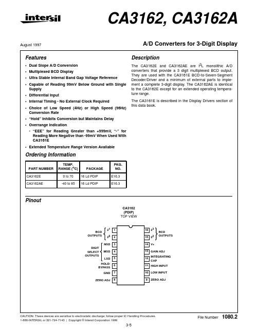
CA3162中文资料
Maximum Storage Temperature Range . . . . . . . . . .-65oC to 150oC
Maximum Lead Temperature (Soldering 10s) . . . . . . . . . . . . . 300oC
CAUTION: Stresses above those listed in “Absolute Maximum Ratings” may cause permanent damage to the device. This is a stress only rating and operation of the device at these or any other conditions above those indicated in the operational sections of this specification is not implied.
3-5
File Number 1080.2
元器件交易网 Functional Block Diagram
CA3162, CA3162A
V+
ZERO ADJ
8
9
HIGH INPUT 11 LOW INPUT 10
V/I CONVERTER
V+
BCD OUTPUTS
INTEGRATING
NOTE: 1. θJA is measured with the component mounted on an evaluation PC board in free air.
Electrical Specifications TA = 25oC, V+ = 5V, Zero Pot Centered, Gain Pot = 2.4kΩ, Unless Otherwise Specified
换热器膨胀节爆裂失效分析研究
- 67 -第3期表1 主要设计参数换热器膨胀节爆裂失效分析研究徐秀耘(江阴德尔热能机械有限公司, 江苏 无锡 214400)[摘 要] 对某在役换热器膨胀节爆裂现象进行了研究,以现场开裂断口进行分析,结合膨胀节标准进行强度校核,查找膨胀节开裂的原因,并对断口处的铁素体含量进行测试,排除疲劳破坏的可能,最终确定为膨胀节因轴向位移产生的组合应力过大,并存在应力腐蚀环境,导致膨胀节被拉伸“脆断”。
通过对换热器膨胀节爆裂失效分析的研究,为设计人员在今后的设计过程中提供参考,避免同类事件再次发生。
[关键词] 膨胀节;开裂;轴向位移作者简介:徐秀耘(1974—),女,江苏无锡人,本科,总工程师,从事压力容器设计二十年,主要研究方向为压力容器优化设计、搅拌系统优化设计、燃烧器低氮燃烧优化设计等。
1 问题描述某换热器的设计,管壳程材料均为S32168不锈钢,金属平均壁温相差较大,存在较大的温差应力,为保证换热管与管板的连接强度,避免换管程/壳程设计压力 MPa 3.6MPa/3.4MPa 管程/壳程筒体和封头材料S32168/ S32168管程/壳程设计温度 ℃320℃/400℃换热管材料S32168(GB13296)储存介质H 2、H 2S 膨胀节名义厚度 mm 14腐蚀裕量 mm 0管程/壳程金属平均壁温 ℃266/336设备内径 mm650换热管规格 mmΦ25×2×4500热管失稳,设计者在壳程设置膨胀节以降低温差应力的影响,设计参数如表1所示,设计原图如图1所示,该换热器在使用不到半年突然出现膨胀节波峰爆裂现象,如图2、图3所示。
2 开裂原因分析膨胀节爆裂使生产被迫停止,迫切需要查找膨胀节失效的原因,为后续的改造提供依据。
初步判断可能是实际工况超载,计算工况与实际不符导致开裂,也可能是因介质中含有H 2S ,导致H 2S 应力腐蚀开裂,也有可能是因热应力疲劳,导致波峰开裂等。
具体开裂原因,本文根据介质特性、膨胀节制造、强度校核等方面进行分析查找,重点考虑以下几个方面:2.1 应力腐蚀开裂应力腐蚀开裂的必要条件是要有拉应力和特定的腐蚀介质存在,裂纹的形成和扩展大致与拉应力方向垂直。
MAX3232EETE+T中文资料
For pricing, delivery, and ordering information, please contact Maxim Direct at 1-888-629-4642,or visit Maxim's website at .General DescriptionThe MAX3222E/MAX3232E/MAX3237E/MAX3241E/MAX3246E +3.0V-powered EIA/TIA-232 and V.28/V.24communications interface devices feature low power con-sumption, high data-rate capabilities, and enhanced electrostatic-discharge (ESD) protection. The enhanced ESD structure protects all transmitter outputs and receiver inputs to ±15kV using IEC 1000-4-2 Air-G ap Discharge, ±8kV using IEC 1000-4-2 Contact Discharge (±9kV for MAX3246E), and ±15kV using the Human Body Model. The logic and receiver I/O pins of the MAX3237E are protected to the above standards, while the transmit-ter output pins are protected to ±15kV using the Human Body Model.A proprietary low-dropout transmitter output stage delivers true RS-232 performance from a +3.0V to +5.5V power supply, using an internal dual charge pump. The charge pump requires only four small 0.1µF capacitors for opera-tion from a +3.3V supply. Each device guarantees opera-tion at data rates of 250kbps while maintaining RS-232output levels. The MAX3237E guarantees operation at 250kbps in the normal operating mode and 1Mbps in the MegaBaud™ operating mode, while maintaining RS-232-compliant output levels.The MAX3222E/MAX3232E have two receivers and two transmitters. The MAX3222E features a 1µA shutdown mode that reduces power consumption in battery-pow-ered portable systems. The MAX3222E receivers remain active in shutdown mode, allowing monitoring of external devices while consuming only 1µA of supply current. The MAX3222E and MAX3232E are pin, package, and func-tionally compatible with the industry-standard MAX242and MAX232, respectively.The MAX3241E/MAX3246E are complete serial ports (three drivers/five receivers) designed for notebook and subnotebook computers. The MAX3237E (five drivers/three receivers) is ideal for peripheral applications that require fast data transfer. These devices feature a shut-down mode in which all receivers remain active, while consuming only 1µA (MAX3241E/MAX3246E) or 10nA (MAX3237E).The MAX3222E, MAX3232E, and MAX3241E are avail-able in space-saving SO, SSOP, TQFN and TSSOP pack-ages. The MAX3237E is offered in an SSOP package.The MAX3246E is offered in the ultra-small 6 x 6 UCSP™package.ApplicationsBattery-Powered Equipment PrintersCell PhonesSmart Phones Cell-Phone Data Cables xDSL ModemsNotebook, Subnotebook,and Palmtop ComputersNext-Generation Device Features♦For Space-Constrained ApplicationsMAX3228E/MAX3229E: ±15kV ESD-Protected, +2.5V to +5.5V, RS-232 Transceivers in UCSP ♦For Low-Voltage or Data Cable ApplicationsMAX3380E/MAX3381E: +2.35V to +5.5V, 1µA, 2Tx/2Rx, RS-232 Transceivers with ±15kV ESD-Protected I/O and Logic PinsMAX3222E/MAX3232E/MAX3237E/MAX3241E †/MAX3246E±15kV ESD-Protected, Down to 10nA, 3.0V to 5.5V ,Up to 1Mbps, True RS-232 Transceivers________________________________________________________________Maxim Integrated Products 119-1298; Rev 11; 10/07Ordering Information continued at end of data sheet.*Dice are tested at T A = +25°C, DC parameters only.**EP = Exposed paddle.Pin Configurations, Selector Guide, and Typical Operating Circuits appear at end of data sheet.MegaBaud and UCSP are trademarks of Maxim Integrated Products, Inc.†Covered by U.S. Patent numbers 4,636,930; 4,679,134;4,777,577; 4,797,899; 4,809,152; 4,897,774; 4,999,761; and other patents pending.M A X 3222E /M A X 3232E /M A X 3237E /M A X 3241E †/M A X 3246EUp to 1Mbps, True RS-232 TransceiversABSOLUTE MAXIMUM RATINGSELECTRICAL CHARACTERISTICS(V CC = +3V to +5.5V, C1–C4 = 0.1µF, T A = T MIN to T MAX , unless otherwise noted. Typical values are at T A = +25°C.) (Notes 3, 4)Stresses beyond those listed under “Absolute Maximum Ratings” may cause permanent damage to the device. These are stress ratings only, and functional operation of the device at these or any other conditions beyond those indicated in the operational sections of the specifications is not implied. Exposure to absolute maximum rating conditions for extended periods may affect device reliability.V CC to GND..............................................................-0.3V to +6V V+ to GND (Note 1)..................................................-0.3V to +7V V- to GND (Note 1)...................................................+0.3V to -7V V+ + |V-| (Note 1).................................................................+13V Input Voltages T_IN, EN , SHDN , MBAUD to GND ........................-0.3V to +6V R_IN to GND.....................................................................±25V Output Voltages T_OUT to GND...............................................................±13.2V R_OUT, R_OUTB (MAX3241E)................-0.3V to (V CC + 0.3V)Short-Circuit Duration, T_OUT to GND.......................Continuous Continuous Power Dissipation (T A = +70°C)16-Pin SSOP (derate 7.14mW/°C above +70°C)..........571mW 16-Pin TSSOP (derate 9.4mW/°C above +70°C).......754.7mW 16-Pin TQFN (derate 20.8mW/°C above +70°C).....1666.7mW 16-Pin Wide SO (derate 9.52mW/°C above +70°C).....762mW 18-Pin Wide SO (derate 9.52mW/°C above +70°C).....762mW 18-Pin PDIP (derate 11.11mW/°C above +70°C)..........889mW 20-Pin TQFN (derate 21.3mW/°C above +70°C)........1702mW 20-Pin TSSOP (derate 10.9mW/°C above +70°C)........879mW 20-Pin SSOP (derate 8.00mW/°C above +70°C)..........640mW 28-Pin SSOP (derate 9.52mW/°C above +70°C)..........762mW 28-Pin Wide SO (derate 12.50mW/°C above +70°C).............1W 28-Pin TSSOP (derate 12.8mW/°C above +70°C)......1026mW 32-Lead Thin QFN (derate 33.3mW/°C above +70°C)..2666mW 6 x 6 UCSP (derate 12.6mW/°C above +70°C).............1010mW Operating Temperature Ranges MAX32_ _EC_ _...................................................0°C to +70°C MAX32_ _EE_ _.................................................-40°C to +85°C Storage Temperature Range.............................-65°C to +150°C Lead Temperature (soldering, 10s).................................+300°C Bump Reflow Temperature (Note 2)Infrared, 15s..................................................................+200°C Vapor Phase, 20s..........................................................+215°C Note 1:V+ and V- can have maximum magnitudes of 7V, but their absolute difference cannot exceed 13V.Note 2:This device is constructed using a unique set of packaging techniques that impose a limit on the thermal profile the devicecan be exposed to during board-level solder attach and rework. This limit permits only the use of the solder profiles recom-mended in the industry-standard specification, JEDEC 020A, paragraph 7.6, Table 3 for IR/VPR and convection reflow.Preheating is required. Hand or wave soldering is not allowed.MAX3222E/MAX3232E/MAX3237E/MAX3241E †/MAX3246EUp to 1Mbps, True RS-232 Transceivers_______________________________________________________________________________________3M A X 3222E /M A X 3232E /M A X 3237E /M A X 3241E †/M A X 3246EUp to 1Mbps, True RS-232 Transceivers4_______________________________________________________________________________________TIMING CHARACTERISTICS—MAX3237E(V CC = +3V to +5.5V, C1–C4 = 0.1µF, T A = T MIN to T MAX , unless otherwise noted. Typical values are at T A = +25°C.) (Note 3)±10%. MAX3237E: C1–C4 = 0.1µF tested at +3.3V ±5%, C1–C4 = 0.22µF tested at +3.3V ±10%; C1 = 0.047µF, C2, C3, C4 =0.33µF tested at +5.0V ±10%. MAX3246E; C1-C4 = 0.22µF tested at +3.3V ±10%; C1 = 0.22µF, C2, C3, C4 = 0.54µF tested at 5.0V ±10%.Note 4:MAX3246E devices are production tested at +25°C. All limits are guaranteed by design over the operating temperature range.Note 5:The MAX3237E logic inputs have an active positive feedback resistor. The input current goes to zero when the inputs are atthe supply rails.Note 6:MAX3241EEUI is specified at T A = +25°C.Note 7:Transmitter skew is measured at the transmitter zero crosspoints.TIMING CHARACTERISTICS—MAX3222E/MAX3232E/MAX3241E/MAX3246EMAX3222E/MAX3232E/MAX3237E/MAX3241E †/MAX3246EUp to 1Mbps, True RS-232 Transceivers_______________________________________________________________________________________5-6-4-202460MAX3237ETRANSMITTER OUTPUT VOLTAGE vs. LOAD CAPACITANCE (MBAUD = GND)LOAD CAPACITANCE (pF)T R A N S M I T T E R O U T P U T V O L T A G E (V )10001500500200025003000531-1-3-5-6-2-42046-5-31-135010001500500200025003000LOAD CAPACITANCE (pF)T R A N S M I T T E R O U T P U T V O L T A G E (V )MAX3237ETRANSMITTER OUTPUT VOLTAGEvs. LOAD CAPACITANCE-7.5-5.0-2.502.55.07.5MAX3237ETRANSMITTER OUTPUT VOLTAGE vs. LOAD CAPACITANCE (MBAUD = V CC )LOAD CAPACITANCE (pF)T R A N S M I T T E R O U T P U T V O L T A G E (V )500100015002000__________________________________________Typical Operating Characteristics(V CC = +3.3V, 250kbps data rate, 0.1µF capacitors, all transmitters loaded with 3k Ωand C L , T A = +25°C, unless otherwise noted.)-6-5-4-3-2-10123456010002000300040005000MAX3241ETRANSMITTER OUTPUT VOLTAGEvs. LOAD CAPACITANCELOAD CAPACITANCE (pF)T R A N S M I T T E R O U T P U T V O L T A G E (V)302010405060020001000300040005000MAX3241EOPERATING SUPPLY CURRENT vs. LOAD CAPACITANCELOAD CAPACITANCE (pF)S U P P L Y C U R R E N T (m A )04286121014010002000300040005000MAX3241ESLEW RATE vs. LOAD CAPACITANCEM A X 3237E t o c 05LOAD CAPACITANCE (pF)S L E W R A T E (V /μs )-6-5-4-3-2-10123456010002000300040005000MAX3222E/MAX3232ETRANSMITTER OUTPUT VOLTAGEvs. LOAD CAPACITANCELOAD CAPACITANCE (pF)T R A N S M I T T E R O U T P UT V O L T A G E (V )624108141216010002000300040005000MAX3222E/MAX3232ESLEW RATE vs. LOAD CAPACITANCELOAD CAPACITANCE (pF)S L E W R A T E (V /μs)2520155103530404520001000300040005000MAX3222E/MAX3232E OPERATING SUPPLY CURRENT vs. LOAD CAPACITANCELOAD CAPACITANCE (pF)S U P P L Y C U R R E N T (m A )M A X 3222E /M A X 3232E /M A X 3237E /M A X 3241E †/M A X 3246EUp to 1Mbps, True RS-232 Transceivers6_______________________________________________________________________________________Typical Operating Characteristics (continued)(V CC = +3.3V, 250kbps data rate, 0.1µF capacitors, all transmitters loaded with 3k Ωand C L , T A = +25°C, unless otherwise noted.)20604080100MAX3237ETRANSMITTER SKEW vs. LOAD CAPACITANCE(MBAUD = V CC )LOAD CAPACITANCE (pF)100015005002000T R A N S M I T T E R S K E W (n s )-6-2-42046-3-51-1352.03.03.52.54.04.55.0SUPPLY VOLTAGE (V)T R A N S M I T T E R O U T P U T V O L T A G E (V )MAX3237ETRANSMITTER OUTPUT VOLTAGE vs. SUPPLY VOLTAGE (MBAUD = GND)10203040502.0MAX3237E SUPPLY CURRENT vs. SUPPLY VOLTAGE (MBAUD = GND)SUPPLY VOLTAGE (V)S U P P L Y C U R R E N T (m A )3.03.52.54.04.55.0MAX3246ETRANSMITTER OUTPUT VOLTAGEvs. LOAD CAPACITANCELOAD CAPACITANCE (pF)T R A N S M I T T E R O U T P U T V O L T A G E (V )4000300010002000-5-4-3-2-101234567-65000468101214160MAX3246ESLEW RATE vs. LOAD CAPACITANCELOAD CAPACITANCE (pF)S L EW R A T E (V /μs )200030001000400050001020304050600MAX3246EOPERATING SUPPLY CURRENT vs. LOAD CAPACITANCEM A X 3237E t o c 17LOAD CAPACITANCE (pF)S U P P L Y C U R R EN T (m A )1000200030004000500055453525155024681012MAX3237ESLEW RATE vs. LOAD CAPACITANCE(MBAUD = GND)LOAD CAPACITANCE (pF)S L E W R A T E (V /μs )10001500500200025003000010203050406070MAX3237ESLEW RATE vs. LOAD CAPACITANCE(MBAUD = V CC )LOAD CAPACITANCE (pF)S L E W R A T E (V /μs )5001000150020001020304050MAX3237ESUPPLY CURRENT vs. LOAD CAPACITANCE WHEN TRANSMITTING DATA (MBAUD = GND)LOAD CAPACITANCE (pF)S U P P L Y C U R R E N T (m A )10001500500200025003000MAX3222E/MAX3232E/MAX3237E/MAX3241E †/MAX3246EUp to 1Mbps, True RS-232 Transceivers_______________________________________________________________________________________7Pin DescriptionM A X 3222E /M A X 3232E /M A X 3237E /M A X 3241E †/M A X 3246EUp to 1Mbps, True RS-232 Transceivers8_______________________________________________________________________________________MAX3222E/MAX3232E/MAX3237E/MAX3241E †/MAX3246EUp to 1Mbps, True RS-232 Transceivers_______________________________________________________________________________________9Detailed DescriptionDual Charge-Pump Voltage ConverterThe MAX3222E/MAX3232E/MAX3237E/MAX3241E/MAX3246Es’ internal power supply consists of a regu-lated dual charge pump that provides output voltages of +5.5V (doubling charge pump) and -5.5V (inverting charge pump) over the +3.0V to +5.5V V CC range. The charge pump operates in discontinuous mode; if the output voltages are less than 5.5V, the charge pump is enabled, and if the output voltages exceed 5.5V, the charge pump is disabled. Each charge pump requires a flying capacitor (C1, C2) and a reservoir capacitor (C3, C4) to generate the V+ and V- supplies (Figure 1).RS-232 TransmittersThe transmitters are inverting level translators that con-vert TTL/CMOS-logic levels to ±5V EIA/TIA-232-compli-ant levels.The MAX3222E/MAX3232E/MAX3237E/MAX3241E/MAX3246E transmitters guarantee a 250kbps data rate with worst-case loads of 3k Ωin parallel with 1000pF,providing compatibility with PC-to-PC communication software (such as LapLink™). Transmitters can be par-alleled to drive multiple receivers or mice.The MAX3222E/MAX3237E/MAX3241E/MAX3246E transmitters are disabled and the outputs are forcedinto a high-impedance state when the device is in shut-down mode (SHDN = G ND). The MAX3222E/MAX3232E/MAX3237E/MAX3241E/MAX3246E permit the outputs to be driven up to ±12V in shutdown.The MAX3222E/MAX3232E/MAX3241E/MAX3246E transmitter inputs do not have pullup resistors. Connect unused inputs to GND or V CC . The MAX3237E’s trans-mitter inputs have a 400k Ωactive positive-feedback resistor, allowing unused inputs to be left unconnected.MAX3237E MegaBaud OperationFor higher-speed serial communications, the MAX3237E features MegaBaud operation. In MegaBaud operating mode (MBAUD = V CC ), the MAX3237E transmitters guarantee a 1Mbps data rate with worst-case loads of 3k Ωin parallel with 250pF for +3.0V < V CC < +4.5V. For +5V ±10% operation, the MAX3237E transmitters guarantee a 1Mbps data rate into worst-case loads of 3k Ωin parallel with 1000pF.RS-232 ReceiversThe receivers convert RS-232 signals to CMOS-logic output levels. The MAX3222E/MAX3237E/MAX3241E/MAX3246E receivers have inverting three-state outputs.Drive EN high to place the receiver(s) into a high-impedance state. Receivers can be either active or inactive in shutdown (Table 1).Figure 1. Slew-Rate Test CircuitsLapLink is a trademark of Traveling Software.M A X 3222E /M A X 3232E /M A X 3237E /M A X 3241E †/M A X 3246EUp to 1Mbps, True RS-232 Transceivers10______________________________________________________________________________________The complementary outputs on the MAX3237E/MAX3241E (R_OUTB) are always active, regardless of the state of EN or SHDN . This allows the device to be used for ring indicator applications without forward biasing other devices connected to the receiver outputs. This is ideal for systems where V CC drops to zero in shutdown to accommodate peripherals such as UARTs (Figure 2).MAX3222E/MAX3237E/MAX3241E/MAX3246E Shutdown ModeSupply current falls to less than 1µA in shutdown mode (SHDN = low). The MAX3237E’s supply current falls to10nA (typ) when all receiver inputs are in the invalid range (-0.3V < R_IN < +0.3). When shut down, the device’s charge pumps are shut off, V+ is pulled down to V CC , V- is pulled to ground, and the transmitter out-puts are disabled (high impedance). The time required to recover from shutdown is typically 100µs, as shown in Figure 3. Connect SHDN to V CC if shutdown mode is not used. SHDN has no effect on R_OUT or R_OUTB (MAX3237E/MAX3241E).±15kV ESD ProtectionAs with all Maxim devices, ESD-protection structures are incorporated to protect against electrostatic dis-charges encountered during handling and assembly.The driver outputs and receiver inputs of the MAX3222E/MAX3232E/MAX3237E/MAX3241E/MAX3246E have extra protection against static electricity. Maxim’s engineers have developed state-of-the-art structures to protect these pins against ESD of ±15kV without damage.The ESD structures withstand high ESD in all states:normal operation, shutdown, and powered down. After an ESD event, Maxim’s E versions keep working without latchup, whereas competing RS-232 products can latch and must be powered down to remove latchup.Furthermore, the MAX3237E logic I/O pins also have ±15kV ESD protection. Protecting the logic I/O pins to ±15kV makes the MAX3237E ideal for data cable applications.SHDN T2OUTT1OUT5V/div2V/divV CC = 3.3V C1–C4 = 0.1μFFigure 3. Transmitter Outputs Recovering from Shutdown or Powering UpMAX3222E/MAX3232E/MAX3237E/MAX3241E †/MAX3246EUp to 1Mbps, True RS-232 TransceiversESD protection can be tested in various ways; the transmitter outputs and receiver inputs for the MAX3222E/MAX3232E/MAX3241E/MAX3246E are characterized for protection to the following limits:•±15kV using the Human Body Model•±8kV using the Contact Discharge method specified in IEC 1000-4-2•±9kV (MAX3246E only) using the Contact Discharge method specified in IEC 1000-4-2•±15kV using the Air-G ap Discharge method speci-fied in IEC 1000-4-2Figure 4a. Human Body ESD Test ModelFigure 4b. Human Body Model Current WaveformFigure 5a. IEC 1000-4-2 ESD Test Model Figure 5b. IEC 1000-4-2 ESD Generator Current WaveformM A X 3222E /M A X 3232E /M A X 3237E /M A X 3241E †/M A X 3246EUp to 1Mbps, True RS-232 Transceiverscharacterized for protection to ±15kV per the Human Body Model.ESD Test ConditionsESD performance depends on a variety of conditions.Contact Maxim for a reliability report that documents test setup, test methodology, and test results.Human Body ModelFigure 4a shows the Human Body Model, and Figure 4b shows the current waveform it generates when dis-charged into a low impedance. This model consists of a 100pF capacitor charged to the ESD voltage of interest,which is then discharged into the test device through a 1.5k Ωresistor.IEC 1000-4-2The IEC 1000-4-2 standard covers ESD testing and performance of finished equipment; it does not specifi-cally refer to integrated circuits. The MAX3222E/MAX3232E/MAX3237E/MAX3241E/MAX3246E help you design equipment that meets level 4 (the highest level)of IEC 1000-4-2, without the need for additional ESD-protection components.The major difference between tests done using the Human Body Model and IEC 1000-4-2 is higher peak current in IEC 1000-4-2, because series resistance is lower in the IEC 1000-4-2 model. Hence, the ESD with-stand voltage measured to IEC 1000-4-2 is generally lower than that measured using the Human Body Model. Figure 5a shows the IEC 1000-4-2 model, and Figure 5b shows the current waveform for the ±8kV IEC 1000-4-2 level 4 ESD Contact Discharge test. The Air-G ap Discharge test involves approaching the device with a charged probe. The Contact Discharge method connects the probe to the device before the probe is energized.Machine ModelThe Machine Model for ESD tests all pins using a 200pF storage capacitor and zero discharge resis-tance. Its objective is to emulate the stress caused by contact that occurs with handling and assembly during manufacturing. All pins require this protection during manufacturing, not just RS-232 inputs and outputs.Therefore, after PC board assembly, the Machine Model is less relevant to I/O ports.Table 2. Required Minimum Capacitor ValuesFigure 6a. MAX3241E Transmitter Output Voltage vs. Load Current Per TransmitterTable 3. Logic-Family Compatibility with Various Supply VoltagesMAX3222E/MAX3232E/MAX3237E/MAX3241E †/MAX3246EUp to 1Mbps, True RS-232 TransceiversApplications InformationCapacitor SelectionThe capacitor type used for C1–C4 is not critical for proper operation; polarized or nonpolarized capacitors can be used. The charge pump requires 0.1µF capaci-tors for 3.3V operation. For other supply voltages, see Table 2 for required capacitor values. Do not use val-ues smaller than those listed in Table 2. Increasing the capacitor values (e.g., by a factor of 2) reduces ripple on the transmitter outputs and slightly reduces power consumption. C2, C3, and C4 can be increased without changing C1’s value. However, do not increase C1without also increasing the values of C2, C3, C4,and C BYPASS to maintain the proper ratios (C1 to the other capacitors).When using the minimum required capacitor values,make sure the capacitor value does not degradeexcessively with temperature. If in doubt, use capaci-tors with a larger nominal value. The capacitor’s equiv-alent series resistance (ESR), which usually rises at low temperatures, influences the amount of ripple on V+and V-.Power-Supply DecouplingIn most circumstances, a 0.1µF V CC bypass capacitor is adequate. In applications sensitive to power-supply noise, use a capacitor of the same value as charge-pump capacitor C1. Connect bypass capacitors as close to the IC as possible.Operation Down to 2.7VTransmitter outputs meet EIA/TIA-562 levels of ±3.7V with supply voltages as low as 2.7V.Figure 6b. Mouse Driver Test CircuitM A X 3222E /M A X 3232E /M A X 3237E /M A X 3241E †/M A X 3246EUp to 1Mbps, True RS-232 TransceiversFigure 7. Loopback Test CircuitT1IN T1OUTR1OUT5V/div5V/div5V/divV CC = 3.3V C1–C4 = 0.1μFFigure 8. MAX3241E Loopback Test Result at 120kbps T1INT1OUTR1OUT5V/div5V/div5V/divV CC = 3.3V, C1–C4 = 0.1μFFigure 9. MAX3241E Loopback Test Result at 250kbps+5V 0+5V 0-5V +5VT_INT_OUT5k Ω + 250pFR_OUTV CC = 3.3V C1–C4 = 0.1μFFigure 10. MAX3237E Loopback Test Result at 1000kbps (MBAUD = V CC )Transmitter Outputs Recoveringfrom ShutdownFigure 3 shows two transmitter outputs recovering from shutdown mode. As they become active, the two trans-mitter outputs are shown going to opposite RS-232 levels (one transmitter input is high; the other is low). Each transmitter is loaded with 3k Ωin parallel with 2500pF.The transmitter outputs display no ringing or undesir-able transients as they come out of shutdown. Note thatthe transmitters are enabled only when the magnitude of V- exceeds approximately -3.0V.Mouse DrivabilityThe MAX3241E is designed to power serial mice while operating from low-voltage power supplies. It has been tested with leading mouse brands from manu-facturers such as Microsoft and Logitech. The MAX3241E successfully drove all serial mice tested and met their current and voltage requirements.MAX3222E/MAX3232E/MAX3237E/MAX3241E †/MAX3246EUp to 1Mbps, True RS-232 TransceiversFigure 6a shows the transmitter output voltages under increasing load current at +3.0V. Figure 6b shows a typical mouse connection using the MAX3241E.High Data RatesThe MAX3222E/MAX3232E/MAX3237E/MAX3241E/MAX3246E maintain the RS-232 ±5V minimum transmit-ter output voltage even at high data rates. Figure 7shows a transmitter loopback test circuit. Figure 8shows a loopback test result at 120kbps, and Figure 9shows the same test at 250kbps. For Figure 8, all trans-mitters were driven simultaneously at 120kbps into RS-232 loads in parallel with 1000pF. For Figure 9, a single transmitter was driven at 250kbps, and all transmitters were loaded with an RS-232 receiver in parallel with 1000pF.The MAX3237E maintains the RS-232 ±5.0V minimum transmitter output voltage at data rates up to 1Mbps.Figure 10 shows a loopback test result at 1Mbps with MBAUD = V CC . For Figure 10, all transmitters were loaded with an RS-232 receiver in parallel with 250pF.Interconnection with 3V and 5V LogicThe MAX3222E/MAX3232E/MAX3237E/MAX3241E/MAX3246E can directly interface with various 5V logic families, including ACT and HCT CMOS. See Table 3for more information on possible combinations of inter-connections.UCSP ReliabilityThe UCSP represents a unique packaging form factor that may not perform equally to a packaged product through traditional mechanical reliability tests. UCSP reliability is integrally linked to the user’s assembly methods, circuit board material, and usage environ-ment. The user should closely review these areas when considering use of a UCSP package. Performance through Operating Life Test and Moisture Resistance remains uncompromised as the wafer-fabrication process primarily determines it.Mechanical stress performance is a greater considera-tion for a UCSP package. UCSPs are attached through direct solder contact to the user’s PC board, foregoing the inherent stress relief of a packaged product lead frame. Solder joint contact integrity must be consid-ered. Table 4 shows the testing done to characterize the UCSP reliability performance. In conclusion, the UCSP is capable of performing reliably through envi-ronmental stresses as indicated by the results in the table. Additional usage data and recommendations are detailed in the UCSP application note, which can be found on Maxim’s website at .Table 4. Reliability Test DataM A X 3222E /M A X 3232E /M A X 3237E /M A X 3241E †/M A X 3246EUp to 1Mbps, True RS-232 Transceivers__________________________________________________________Pin ConfigurationsMAX3222E/MAX3232E/MAX3237E/MAX3241E †/MAX3246EUp to 1Mbps, True RS-232 TransceiversPin Configurations (continued)M A X 3222E /M A X 3232E /M A X 3237E /M A X 3241E †/M A X 3246EUp to 1Mbps, True RS-232 Transceivers__________________________________________________Typical Operating CircuitsMAX3222E/MAX3232E/MAX3237E/MAX3241E †/MAX3246EUp to 1Mbps, True RS-232 Transceivers_____________________________________Typical Operating Circuits (continued)M A X 3222E /M A X 3232E /M A X 3237E /M A X 3241E †/M A X 3246EUp to 1Mbps, True RS-232 Transceivers_____________________________________Typical Operating Circuits (continued)MAX3222E/MAX3232E/MAX3237E/MAX3241E †/MAX3246EUp to 1Mbps, True RS-232 Transceivers______________________________________________________________________________________21Selector Guide___________________Chip InformationTRANSISTOR COUNT:MAX3222E/MAX3232E: 1129MAX3237E: 2110MAX3241E: 1335MAX3246E: 842PROCESS: BICMOSOrdering Information (continued)†Requires solder temperature profile described in the AbsoluteMaximum Ratings section. UCSP Reliability is integrally linked to the user’s assembly methods, circuit board material, and environment. Refer to the UCSP Reliability Notice in the UCSP Reliability section of this datasheet for more information.**EP = Exposed paddle.。
MAX3232EPE+中文资料

________________General DescriptionThe MAX3222/MAX3232/MAX3237/MAX3241 trans-ceivers have a proprietary low-dropout transmitter out-put stage enabling true RS-232 performance from a 3.0V to 5.5V supply with a dual charge pump. The devices require only four small 0.1µF external charge-pump capacitors. The MAX3222, MAX3232, and MAX3241 are guaranteed to run at data rates of 120kbps while maintaining RS-232 output levels. The MAX3237 is guaranteed to run at data rates of 250kbps in the normal operating mode and 1Mbps in the MegaBaud™ operating mode, while maintaining RS-232output levels.The MAX3222/MAX3232 have 2 receivers and 2 drivers. The MAX3222 features a 1µA shutdown mode that reduces power consumption and extends battery life in portable systems. Its receivers remain active in shutdown mode, allowing external devices such as modems to be monitored using only 1µA supply cur-rent. The MAX3222 and MAX3232 are pin, package,and functionally compatible with the industry-standard MAX242 and MAX232, respectively.The MAX3241 is a complete serial port (3 drivers/5 receivers) designed for notebook and subnotebook computers. The MAX3237 (5 drivers/3 receivers) is ideal for fast modem applications. Both these devices feature a shutdown mode in which all receivers can remain active while using only 1µA supply current. Receivers R1(MAX3237/MAX3241) and R2 (MAX3241) have extra out-puts in addition to their standard outputs. These extra outputs are always active, allowing external devices such as a modem to be monitored without forward bias-ing the protection diodes in circuitry that may have V CC completely removed.The MAX3222, MAX3237, and MAX3241 are available in space-saving TSSOP and SSOP packages.________________________ApplicationsNotebook, Subnotebook, and Palmtop Computers High-Speed Modems Battery-Powered Equipment Hand-Held Equipment Peripherals Printers__Next Generation Device Features♦For Smaller Packaging:MAX3228E/MAX3229E: +2.5V to +5.5V RS-232Transceivers in UCSP™♦For Integrated ESD Protection:MAX3222E/MAX3232E/MAX3237E/MAX3241E*/MAX3246E: ±15kV ESD-Protected, Down to 10nA,3.0V to 5.5V, Up to 1Mbps, True RS-232Transceivers♦For Low-Voltage or Data Cable Applications:MAX3380E/MAX3381E: +2.35V to +5.5V, 1µA, 2 Tx/2 Rx RS-232 Transceivers with ±15kV ESD-Protected I/O and Logic PinsMAX3222/MAX3232/MAX3237/MAX3241*3.0V to 5.5V , Low-Power , up to 1Mbps, T rue RS-232Transceivers Using Four 0.1µF External Capacitors________________________________________________________________Maxim Integrated Products119-0273; Rev 7; 1/07*Covered by U.S. Patent numbers 4,636,930; 4,679,134; 4,777,577; 4,797,899; 4,809,152; 4,897,774; 4,999,761; and other patents pending.Typical Operating Circuits appear at end of data sheet.Ordering Information continued at end of data sheet.For pricing, delivery, and ordering information,please contact Maxim/Dallas Direct!at 1-888-629-4642, or visit Maxim’s website at .+Denotes lead-free package.M A X 3222/M A X 3232/M A X 3237/M A X 3241Transceivers Using Four 0.1µF External Capacitors2_______________________________________________________________________________________ABSOLUTE MAXIMUM RATINGSELECTRICAL CHARACTERISTICS(V CC = +3.0V to +5.5V, C1–C4 = 0.1µF (Note 2), T A = T MIN to T MAX , unless otherwise noted. Typical values are at T A = +25°C.)Stresses beyond those listed under “Absolute Maximum Ratings” may cause permanent damage to the device. These are stress ratings only, and functional operation of the device at these or any other conditions beyond those indicated in the operational sections of the specifications is not implied. Exposure to absolute maximum rating conditions for extended periods may affect device reliability.Note 1:V+ and V- can have a maximum magnitude of 7V, but their absolute difference cannot exceed 13V.V CC ...........................................................................-0.3V to +6V V+ (Note 1)...............................................................-0.3V to +7V V- (Note 1)................................................................+0.3V to -7V V+ + V- (Note 1)...................................................................+13V Input VoltagesT_IN, SHDN , EN ...................................................-0.3V to +6V MBAUD...................................................-0.3V to (V CC + 0.3V)R_IN.................................................................................±25V Output VoltagesT_OUT...........................................................................±13.2V R_OUT....................................................-0.3V to (V CC + 0.3V)Short-Circuit DurationT_OUT....................................................................ContinuousContinuous Power Dissipation (T A = +70°C)16-Pin TSSOP (derate 6.7mW/°C above +70°C).............533mW 16-Pin Narrow SO (derate 8.70mW/°C above +70°C)....696mW 16-Pin Wide SO (derate 9.52mW/°C above +70°C)........762mW 16-Pin Plastic DIP (derate 10.53mW/°C above +70°C)...842mW 18-Pin SO (derate 9.52mW/°C above +70°C)..............762mW 18-Pin Plastic DIP (derate 11.11mW/°C above +70°C)..889mW 20-Pin SSOP (derate 7.00mW/°C above +70°C).........559mW 20-Pin TSSOP (derate 8.0mW/°C above +70°C).............640mW 28-Pin TSSOP (derate 8.7mW/°C above +70°C).............696mW 28-Pin SSOP (derate 9.52mW/°C above +70°C).........762mW 28-Pin SO (derate 12.50mW/°C above +70°C).....................1W Operating Temperature RangesMAX32_ _C_ _.....................................................0°C to +70°C MAX32_ _E_ _ .................................................-40°C to +85°C Storage Temperature Range.............................-65°C to +150°C Lead Temperature (soldering, 10s).................................+300°CMAX3222/MAX3232/MAX3237/MAX3241Transceivers Using Four 0.1µF External Capacitors_______________________________________________________________________________________3TIMING CHARACTERISTICS—MAX3222/MAX3232/MAX3241(V CC = +3.0V to +5.5V, C1–C4 = 0.1µF (Note 2), T A = T MIN to T MAX , unless otherwise noted. Typical values are at T A = +25°C.)ELECTRICAL CHARACTERISTICS (continued)(V CC = +3.0V to +5.5V, C1–C4 = 0.1µF (Note 2), T A = T MIN to T MAX , unless otherwise noted. Typical values are at T A = +25°C.)M A X 3222/M A X 3232/M A X 3237/M A X 3241Transceivers Using Four 0.1µF External Capacitors4_________________________________________________________________________________________________________________________________Typical Operating Characteristics(V CC = +3.3V, 235kbps data rate, 0.1µF capacitors, all transmitters loaded with 3k Ω, T A = +25°C, unless otherwise noted.)-6-5-4-3-2-101234560MAX3222/MAX3232TRANSMITTER OUTPUT VOLTAGEvs. LOAD CAPACITANCELOAD CAPACITANCE (pF)T R A N S M I T T E R O U T P U T V O L T A G E (V )20003000100040005000246810121416182022150MAX3222/MAX3232SLEW RATEvs. LOAD CAPACITANCELOAD CAPACITANCE (pF)S L E W R A T E (V /µs )20003000100040005000510152025303540MAX3222/MAX3232SUPPLY CURRENT vs. LOAD CAPACITANCEWHEN TRANSMITTING DATALOAD CAPACITANCE (pF)S U P P L Y C U R R E N T (m A )20003000100040005000TIMING CHARACTERISTICS—MAX3237(V CC = +3.0V to +5.5V, C1–C4 = 0.1µF (Note 2), T A = T MIN to T MAX , unless otherwise noted. Typical values are at T A = +25°C.)Note 2:MAX3222/MAX3232/MAX3241: C1–C4 = 0.1µF tested at 3.3V ±10%; C1 = 0.047µF, C2–C4 = 0.33µF tested at 5.0V ±10%.MAX3237: C1–C4 = 0.1µF tested at 3.3V ±5%; C1–C4 = 0.22µF tested at 3.3V ±10%; C1 = 0.047µF, C2–C4 = 0.33µF tested at 5.0V ±10%.Note 3:Transmitter input hysteresis is typically 250mV.MAX3222/MAX3232/MAX3237/MAX3241Transceivers Using Four 0.1µF External Capacitors_______________________________________________________________________________________5-7.5-5.0-2.502.55.07.50MAX3241TRANSMITTER OUTPUT VOLTAGEvs. LOAD CAPACITANCELOAD CAPACITANCE (pF)T R A N S M I T T E R O U T P U T V O L T A G E (V )2000300010004000500046810121416182022240MAX3241SLEW RATEvs. LOAD CAPACITANCELOAD CAPACITANCE (pF)S L E W R A T E (V /µs )20003000100040005000510152025303545400MAX3241SUPPLY CURRENT vs. LOADCAPACITANCE WHEN TRANSMITTING DATALOAD CAPACITANCE (pF)S U P P L Y C U R R E N T (m A )20003000100040005000-7.5-5.0-2.502.55.07.50MAX3237TRANSMITTER OUTPUT VOLTAGE vs. LOAD CAPACITANCE (MBAUD = GND)LOAD CAPACITANCE (pF)T R A N S M I T T E R O U T P U T V O L T A G E (V )200030001000400050000102030504060700MAX3237SLEW RATE vs. LOAD CAPACITANCE(MBAUD = V CC )LOAD CAPACITANCE (pF)S L E W R A T E (V /µs )500100015002000-7.5-5.0-2.502.55.07.50MAX3237TRANSMITTER OUTPUT VOLTAGE vs. LOAD CAPACITANCE (MBAUD = V CC )LOAD CAPACITANCE (pF)T R A N S M I T T E R O U T P U T V O L T A G E (V )5001000150020001020304050600MAX3237SUPPLY CURRENT vs.LOAD CAPACITANCE (MBAUD = GND)LOAD CAPACITANCE (pF)S U P P L Y C U R R E N T (m A )200030001000400050000246810120MAX3237SLEW RATE vs. LOAD CAPACITANCE(MBAUD = GND)LOAD CAPACITANCE (pF)S L E W R A T E (V /µs )2000300010004000500010302040506070MAX3237SKEW vs. LOAD CAPACITANCE(t PLH - t PHL )LOAD CAPACITANCE (pF)1000150050020002500_____________________________Typical Operating Characteristics (continued)(V CC = +3.3V, 235kbps data rate, 0.1µF capacitors, all transmitters loaded with 3k Ω, T A = +25°C, unless otherwise noted.)M A X 3222/M A X 3232/M A X 3237/M A X 3241Transceivers Using Four 0.1µF External Capacitors6_____________________________________________________________________________________________________________________________________________________Pin DescriptionMAX3222/MAX3232/MAX3237/MAX3241Transceivers Using Four 0.1µF External Capacitors_______________________________________________________________________________________7_______________Detailed DescriptionDual Charge-Pump Voltage ConverterThe MAX3222/MAX3232/MAX3237/MAX3241’s internal power supply consists of a regulated dual charge pump that provides output voltages of +5.5V (doubling charge pump) and -5.5V (inverting charge pump), regardless of the input voltage (V CC ) over the 3.0V to 5.5V range. The charge pumps operate in a discontinuous mode; if the output voltages are less than 5.5V, the charge pumps are enabled, and if the output voltages exceed 5.5V, the charge pumps are disabled. Each charge pump requires a flying capacitor (C1, C2) and a reservoir capacitor (C3, C4) to generate the V+ and V- supplies.RS-232 TransmittersThe transmitters are inverting level translators that con-vert CMOS-logic levels to 5.0V EIA/TIA-232 levels.The MAX3222/MAX3232/MAX3241 transmitters guaran-tee a 120kbps data rate with worst-case loads of 3k Ωin parallel with 1000pF, providing compatibility with PC-to-PC communication software (such as LapLink™).Typically, these three devices can operate at data rates of 235kbps. Transmitters can be paralleled to drive multi-ple receivers or mice.The MAX3222/MAX3237/MAX3241’s output stage is turned off (high impedance) when the device is in shut-down mode. When the power is off, the MAX3222/MAX3232/MAX3237/MAX3241 permit the outputs to be driven up to ±12V.The transmitter inputs do not have pullup resistors.Connect unused inputs to GND or V CC .MAX3237 MegaBaud OperationIn normal operating mode (MBAUD = G ND), the MAX3237 transmitters guarantee a 250kbps data rate with worst-case loads of 3k Ωin parallel with 1000pF.This provides compatibility with PC-to-PC communica-tion software, such as Laplink.For higher speed serial communications, the MAX3237features MegaBaud operation. In MegaBaud operating mode (MBAUD = V CC ), the MAX3237 transmitters guar-antee a 1Mbps data rate with worst-case loads of 3k Ωin parallel with 250pF for 3.0V < V CC < 4.5V. For 5V ±10%operation, the MAX3237 transmitters guarantee a 1Mbps data rate into worst-case loads of 3k Ωin parallel with 1000pF.Figure 1. Slew-Rate Test CircuitsLapLink is a trademark of Traveling Software, Inc.M A X 3222/M A X 3232/M A X 3237/M A X 3241Transceivers Using Four 0.1µF External Capacitors8_______________________________________________________________________________________RS-232 ReceiversThe receivers convert RS-232 signals to CMOS-logic out-put levels. The MAX3222/MAX3237/MAX3241 receivers have inverting three-state outputs. In shutdown, the receivers can be active or inactive (Table 1).The complementary outputs on the MAX3237 (R1OUTB)and the MAX3241 (R1OUTB, R2OUTB) are always active,regardless of the state of EN or SHDN . This allows for Ring Indicator applications without forward biasing other devices connected to the receiver outputs. This is ideal for systems where V CC is set to 0V in shutdown to accommodate peripherals, such as UARTs (Figure 2).MAX3222/MAX3237/MAX3241Shutdown ModeSupply current falls to less than 1µA in shutdown mode (SHDN = low). When shut down, the device’s charge pumps are turned off, V+ is pulled down to V CC , V- is pulled to ground, and the transmitter outputs are dis-abled (high impedance). The time required to exit shut-down is typically 100µs, as shown in Figure 3. Connect SHDN to V CC if the shutdown mode is not used. SHDN has no effect on R_OUT or R_OUTB.MAX3222/MAX3237/MAX3241Enable ControlThe inverting receiver outputs (R_OUT) are put into a high-impedance state when EN is high. The complemen-tary outputs R1OUTB and R2OUTB are always active,regardless of the state of EN and SHDN (Table 1). EN has no effect on T_OUT.__________Applications InformationCapacitor SelectionThe capacitor type used for C1–C4 is not critical for proper operation; polarized or nonpolarized capacitors can be used. The charge pump requires 0.1µF capaci-tors for 3.3V operation. For other supply voltages, refer to Table 2 for required capacitor values. Do not use values lower than those listed in Table 2. Increasing the capaci-tor values (e.g., by a factor of 2) reduces ripple on the transmitter outputs and slightly reduces power consump-tion. C2, C3, and C4 can be increased without changing C1’s value. However, do not increase C1 without also increasing the values of C2, C3, and C4, to maintain the proper ratios (C1 to the other capacitors).When using the minimum required capacitor values,make sure the capacitor value does not degrade exces-sively with temperature. If in doubt, use capacitors with a higher nominal value. The capacitor’s equivalent series resistance (ESR), which usually rises at low tempera-tures, influences the amount of ripple on V+ and V-.Figure 2. Detection of RS-232 Activity when the UART and Interface are Shut Down; Comparison of MAX3237/MAX3241(b) with Previous Transceivers (a).MAX3222/MAX3232/MAX3237/MAX3241Transceivers Using Four 0.1µF External Capacitors_______________________________________________________________________________________9Power-Supply DecouplingIn most circumstances, a 0.1µF bypass capacitor is adequate. In applications that are sensitive to power-supply noise, decouple V CC to ground with a capacitor of the same value as charge-pump capacitor C1. Connect bypass capacitors as close to the IC as possible.Operation Down to 2.7VTransmitter outputs will meet EIA/TIA-562 levels of ±3.7V with supply voltages as low as 2.7V.Transmitter Outputs whenExiting ShutdownFigure 3 shows two transmitter outputs when exiting shutdown mode. As they become active, the two trans-mitter outputs are shown going to opposite RS-232 lev-els (one transmitter input is high, the other is low).Each transmitter is loaded with 3k Ωin parallel with 2500pF. The transmitter outputs display no ringing or undesirable transients as they come out of shutdown.Note that the transmitters are enabled only when the magnitude of V- exceeds approximately 3V.Mouse DriveabilityThe MAX3241 has been specifically designed to power serial mice while operating from low-voltage power sup-plies. It has been tested with leading mouse brands from manufacturers such as Microsoft and Logitech. The MAX3241 successfully drove all serial mice tested and met their respective current and voltage requirements.Figure 4a shows the transmitter output voltages under increasing load current at 3.0V. Figure 4b shows a typical mouse connection using the MAX3241.CC = 3.3V C1–C4 = 0.1µF50µs/divFigure 3. Transmitter Outputs when Exiting Shutdown or Powering UpM A X 3222/M A X 3232/M A X 3237/M A X 3241Transceivers Using Four 0.1µF External Capacitors10______________________________________________________________________________________Figure 4b. Mouse Driver Test Circuit Figure 4a. MAX3241 Transmitter Output Voltage vs. Load Current per TransmitterMAX3222/MAX3232/MAX3237/MAX3241Transceivers Using Four 0.1µF External Capacitors______________________________________________________________________________________11High Data RatesThe MAX3222/MAX3232/MAX3241 maintain the RS-232±5.0V minimum transmitter output voltage even at high data rates. Figure 5 shows a transmitter loopback test circuit. Figure 6 shows a loopback test result at 120kbps, and Figure 7 shows the same test at 235kbps.For Figure 6, all transmitters were driven simultaneously at 120kbps into RS-232 loads in parallel with 1000pF.For Figure 7, a single transmitter was driven at 235kbps,and all transmitters were loaded with an RS-232 receiver in parallel with 1000pF.The MAX3237 maintains the RS-232 ±5.0V minimum transmitter output voltage at data rates up to 1Mbps.Figure 8 shows a loopback test result at 1Mbps with MBAUD = V CC . For Figure 8, all transmitters were loaded with an RS-232 receiver in parallel with 250pF.CC = 3.3V5µs/divFigure 5. Loopback Test CircuitFigure 6. MAX3241 Loopback Test Result at 120kbpsCC = 3.3V2µs/divFigure 7. MAX3241 Loopback Test Result at 235kbps0V +5V 0V -5V +5V 0VT_INT_OUT = R_IN 5k R_OUT 150pF200ns/divCC = 3.3VFigure 8. MAX3237 Loopback Test Result at 1000kbps (MBAUD = V CC )M A X 3222/M A X 3232/M A X 3237/M A X 3241Transceivers Using Four 0.1µF External Capacitors__________________________________________________Typical Operating CircuitsInterconnection with 3V and 5V LogicThe MAX3222/MAX3232/MAX3237/MAX3241 can directly interface with various 5V logic families, includ-ing ACT and HCT CMOS. See Table 3 for more informa-tion on possible combinations of interconnections.Table 3. Logic-Family Compatibility with Various Supply VoltagesMAX3222/MAX3232/MAX3237/MAX3241Transceivers Using Four 0.1µF External Capacitors______________________________________________________________________________________13_____________________________________Typical Operating Circuits (continued)M A X 3222/M A X 3232/M A X 3237/M A X 3241Transceivers Using Four 0.1µF External Capacitors14___________________________________________________________________________________________________________________________________Pin Configurations (continued)MAX3222/MAX3232/MAX3237/MAX3241Transceivers Using Four 0.1µF External Capacitors______________________________________________________________________________________15______3V-Powered EIA/TIA-232 and EIA/TIA-562 Transceivers from MaximOrdering Information (continued)*Dice are tested at T A = +25°C, DC parameters only.+Denotes lead-free package.M A X 3222/M A X 3232/M A X 3237/M A X 3241Transceivers Using Four 0.1µF External Capacitors16_________________________________________________________________________________________________________Chip Topography___________________Chip InformationT1INT2IN 0.127"(3.225mm)0.087"(2.209mm)R2OUTR2IN T2OUTV CCV+C1+SHDNENC1- C2+C2-V-MAX3222TRANSISTOR COUNT: 339SUBSTRATE CONNECTED TO GNDTransceivers Using Four 0.1µF External CapacitorsPackage Information (The package drawing(s) in this data sheet may not reflect the most current specifications. For the latest package outline information, go to /packages.)Revision HistoryPages changed at Rev 7: 1, 15, 16, 17Maxim cannot assume responsibility for use of any circuitry other than circuitry entirely embodied in a Maxim product. No circuit patent licenses are implied. Maxim reserves the right to change the circuitry and specifications without notice at any time.17__________________Maxim Integrated Products, 120 San Gabriel Drive, Sunnyvale, CA 94086 (408) 737-7600©2007 Maxim Integrated Products is a registered trademark of Maxim Integrated Products, Inc.。
【江苏省自然科学基金】_现代研究_期刊发文热词逐年推荐_20140814
107 108 109 110 111 112 113 114 115 116 117 118 119 120 121 122 123 124 125 126 127 128 129 130 131 132 133 134 135 136 137 138 139 140 141 142 143 144 145 146 147 148 149 150 151 152 153 154 155 156 18 59 60 61 62 63 64 65 66 67 68 69 70 71 72 73 74 75 76 77 78 79 80 81 82 83 84 85 86 87 88 89 90 91 92 93 94 95 96 97 98 99 100 101 102 103 104 105 106
干预 工艺 工作流 嵌合抗体 屈曲稳定 小麦 射频识别 实时 契约 大孔树脂 大功率超声波电源 多光谱图像 夏枯草 复方野马追胶囊 声场 垂跨比 地区经济 图像融合 图像复原 商业化背景 含水率 合理性 合成 可见光 可溶性表达 受体亚型 反相高效液相色谱 参数优选 压电泵 南方红豆杉 单克隆抗体 协调发展 力学特性 分子标记 分割 冠状动脉粥样硬化 内皮细胞 内皮功能 光催化 储藏 信息熵 伺服系统 仿真 人工湿地 产量 乌骨藤 主动队列管理 丹顶鹤 临床应用 专家自适应pid控制 不变量 β -淀粉样蛋白 α 1肾上腺素受体 tio2
遮荫 遗传多样性 逻辑网格 通脉益智方 近红外光谱法 输送性 轴流风送 身份认证 路由算法 距离估计 足细胞 超连续光谱 超细涂料 超支化聚(酰胺-酯)分散剂 超支化分散剂 超微结构 超声波辅助蠕动磨削 资源共享 谷蛋白大聚合体(gmp) 谷粒 调制不稳 诱导抗性 误报率 评价指标 计算机数字控制 观察指标 覆盖 表面活性素 表面形态 表达效率 补肾活血舒筋 血管生成 血管性痴呆 血管内皮生长促进因子 血清型 蛋白质含量 蒙特卡罗 营养需求 药理作用 药敏试验 药对 茶叶 苯酚 自动信任协商 膜分离 脱氢枞酸(β -甲基丙烯酰氧基丙基)酯 脑源性神经营养因子 胃癌 肿瘤 肾上腺素受体 肺癌 肉类产业 聚合物 羟基萘酚
AP3216SYC;中文规格书,Datasheet资料
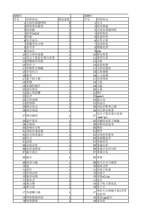
Note: 1. θ1/2 is the angle from optical centerline where the luminous intensity is 1/2 the optical centerline value.
Description
The Super Bright Yellow device is made with DH InGaAlP (on GaAs substrate) light emitting diode chip.
Package Dimensions
Notes: 1. All dimensions are in millimeters (inches). 2. Tolerance is ±0.2(0.008") unless otherwise noted. 3. Specifications are subject to change without notice.
SPEC NO: DSAB1130 APPROVED: J. Lu
REV NO: V.5 CHECKED: Allen Liu
DATE: MAR/10/2005 DRAWN: Y.CHENG
PAGE: 1 OF 4 ERP: 1203000427
/
Selection Guide
DATE: MAR/10/2005 DRAWN: Y.CHENG
PAGE: 3 OF 4 ERP: 1203000427
落实语用,提升表达
语文课堂YuWenKeTang教师·TEACHER0202019年8月Aug.2019常年在低段教学中笔者发现,有些学生上课不举手,缺乏表达的勇气;有些学生思路清楚但是表达非所想;还有的学生在写话中语言枯燥,表达无序。
一方面与这个学段的学生认知积累有关,另一方面则是由于学生习得知识却不会运用。
《义务教育语文课程标准(2011年版)》(以下简称《课标》)明确提出:“语文课程致力于培养学生的语言文字运用能力,提升学生的综合素养。
”也就是说,语文教学要让学生在课堂实践中树立语用意识,掌握语言运用的方法,提高学生口头和书面语言的表达能力。
低年级学生正处于表达发展的启蒙阶段,是儿童学习书面表达的开始。
因此语用教学有必要从低年级课堂展开。
笔者立足文本,从基础的“字词句”出发,指导学生语言文字的运用。
本文以部编版低年级教材为例谈谈几点做法:一、巧借字理,激活表达在课堂上语言文字的运用常见于阅读教学或者作文教学中,而在识字教学中却常常被忽略。
对于低年级的学生,识字是一块重要的学习内容。
教师应更加有意识地将识字和迁移运用相结合。
中国的汉字是集音、形、义于一体的表意文字,具有图画性、表义性,富有丰富文化意蕴。
教师孤立地将汉字的音、形、义拆解开,让学生生硬地识记字形,学生难以真正地理解汉字的意思。
对于低年级的学生来说,形象思维占主导地位,借助字理教学,追溯字源,启发学生想象,形象感知汉字的意思,既符合低段学生学习的心理特点,又高效拓展识字量,激发学生的表达兴趣。
例如,在一年级下册《四个太阳》“道”字的教学中,笔者是这样实施的:先是出示“道”的生字和拼音,请小老师带读。
然后出示图片,让学生观察图上画了什么。
学生回答一个人在路上走。
笔者联系旧知“首”的本义:“仔细看‘道’字,走,我们已经学过表示走路的意思,哪一部分表示人的意思呢?” 接着教授学生“道”的意思:“首的古义指头,在这儿表示人。
因此‘道’的本义是路的意思。
32169化学成分
32169化学成分
32169不锈钢,也称为S32169,是一种具有优秀耐腐蚀性的高合金奥氏体不锈钢。
这种不锈钢在各种腐蚀环境中表现出色,如氯化物、氯气、硫酸等。
化学成分是决定32169不锈钢性能的关键因素。
在标准范围内,其化学成分如下:
* 铬(Cr):24.00% - 26.00%
* 镍(Ni):13.00% - 15.00%
* 钼(Mo):3.00% - 5.00%
* 铜(Cu):0.50% - 2.00%
* 氮(N):0.24% - 0.32%
* 铁(Fe):余量
这些元素在不锈钢中的比例决定了其耐腐蚀性、强度和加工性能。
例如,铬元素有助于形成保护性的氧化膜,防止腐蚀;镍元素则有助于提高耐腐蚀性和韧性;而氮和钛的加入则有助于提高强度和焊接性能。
此外,32169不锈钢还含有一定量的钛(Ti)和铝(Al),这些元素有助于细化钢的组织结构,提高其机械性能。
需要注意的是,化学成分的含量会根据不同的生产厂家和工艺略有差异。
因此,在实际应用中,需要根据具体的使用环境和要求选择合适的32169不锈钢产品。
329332资料
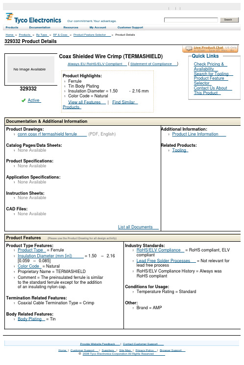
329332 Product DetailsHome | Customer Support | Suppliers | Site Map | Privacy Policy | Browser Support© 2008 Tyco Electronics Corporation All Rights Reserved SearchProducts Documentation Resources My Account Customer Support Home > Products > By Type > RF & Coax > Product Feature Selector > Product DetailsNo Image Available329332Active Coax Shielded Wire Crimp (TERMASHIELD)Always EU RoHS/ELV Compliant (Statement of Compliance)Product Highlights:?Ferrule?Tin Body Plating?Insulation Diameter = 1.50 - 2.16 mm?Color Code = NaturalView all Features | Find SimilarProductsCheck Pricing &AvailabilitySearch for ToolingProduct FeatureSelectorContact Us AboutThis ProductQuick LinksDocumentation & Additional InformationProduct Drawings:?conn coax rf termashield ferrule(PDF, English)Catalog Pages/Data Sheets:?None AvailableProduct Specifications:?None AvailableApplication Specifications:?None AvailableInstruction Sheets:?None AvailableCAD Files:?None AvailableList all Documents Additional Information:?Product Line InformationRelated Products:?ToolingProduct Features (Please use the Product Drawing for all design activity)Product Type Features:?Product Type = Ferrule?Insulation Diameter (mm [in]) = 1.50 – 2.16[0.059 –0.085]?Color Code = Natural?Proprietary Name = TERMASHIELD?Comment = The preinsulated ferrule is similarto the standard ferrule except for the additionof an insulating nylon cap.Termination Related Features:?Coaxial Cable Termination Type = CrimpBody Related Features:?Body Plating = Tin Industry Standards:?RoHS/ELV Compliance = RoHS compliant, ELVcompliant?Lead Free Solder Processes = Not relevant forlead free process?RoHS/ELV Compliance History = Always wasRoHS compliantConditions for Usage:?Temperature Rating = StandardOther:?Brand = AMPProvide Website Feedback | Contact Customer Support。
T8163-2008无缝钢管标准与规格表

本标准与10216-1:2004《用于
压力的无缝钢管交货技术条件
第一部分:规定室温性能的非合
金钢管》的一致性程度为非等
效。
无缝钢管
本标准代替GB/T8163-1999《输
送流体用无缝钢管》。
本标准与
GB/T8163-1999相比,主要变化
如下:
——增加了订货内容;
——修改了尺寸允许偏差;
——增加了全长弯曲度要
求;
——增加了端头切斜要求;
——取消了标记示例;
——增加了钢牌号;
——修改了Q345的屈服强
度;
——对按钢级交货,质量等
级B及以上的铜牌号增加了冲击
试验要求;
——修改了组批规则。
本标准所代替标准的历次
版本发布情况为:
——GB/T8163-1987、
GB/T8163-1999
———2008-08-19发布20
材质:20# GB
/T8163-2008
无缝钢管
材质:20# GB
/T8163-2008
无缝钢管。
- 1、下载文档前请自行甄别文档内容的完整性,平台不提供额外的编辑、内容补充、找答案等附加服务。
- 2、"仅部分预览"的文档,不可在线预览部分如存在完整性等问题,可反馈申请退款(可完整预览的文档不适用该条件!)。
- 3、如文档侵犯您的权益,请联系客服反馈,我们会尽快为您处理(人工客服工作时间:9:00-18:30)。
Industry Standards: Government/Industry Qualification = No RoHS/ELV Compliance = RoHS compliant, ELV compliant Lead Free Solder Processes = Not relevant for lead free process RoHS/ELV Compliance History = Always was RoHS compliant Packaging Related Features: Packaging Method = Loose Piece Other: Brand = AMP
Ring and Spade Tongue Terminals
Always EU RoHS/ELV Compliant (Statement of Compliance)
Quick Links
Check Pricing & Availability Search for Tooling Product Feature Selector Contact Us About This Product
Product Highlights:
321632
Active
Terminal Shape = Hook Tongue Receptacle Style = Straight Body Style = SOLISTRAND Barrel Type = Closed Barrel Wire/Cable Type = Regular Wire View all Features | Find Similar Products
Documentation & Additional Information Product Drawings: TERMINAL, HOOK TONGUE, SOLISTRAND (PDF, English) Catalog Pages/Data Sheets: SOLISTRAND BUDGET AND DIAMOND GRIP UNINSULATED TERMI... (PDF, English) Product Specifications: None Available Application Specifications: None Available Instruction Sheets: None Available CAD Files: (CAD Format & Compression Information) 2D Drawing (DXF, Version D) 3D Model (IGES, Version D) 3D Model (STEP, Version D) Additional Information: Product Line Information Related Products: Tooling
/TE/bin/TE.Connect?C=1&M=BYPN&TCPN=321632&RQPN=321632
2/5/2008
2/5/2008
元器件交易网
321632 Product Details - Tyco Electronics
Page 2 of 2
Product Type Features: Terminal Shape = Hook Tongue Receptacle Style = Straight Body Style = SOLISTRAND Barrel Type = Closed Barrel Wire/Cable Type = Regular Wire Insulation = No Insulation Support = Non-Insulation Support Stud Size = 1/4 [M6] Stud Diameter (mm [in]) = 6.35 [0.250] Shape = SPADE-050 Heavy Duty = No Material = Copper Finish = Tin Body Related Features: Wire Range (mm [AWG]) = 3.00-6.00² [12-10] Wire Range (CMA) = 5,180 – 13,100 Barrel I.D. Min. (mm [in]) = 3.28 [0.129] Stock Thickness (mm [in]) = 1.07 [0.042]
List all Documents
Product Features (Please use the Product Drawing for all design activity)
/TE/bin/TE.Connect?C=1&M=BYPN&TCPN=321632&RQPN=321632
321632 Product Details - Tyco 元器件交易网 Electronics
Page 1 of 2
Corporate Home |
Electronic Components | Segments | Who We Ar32 Product Details
Provide Website Feedback | Contact Customer Support
Home | Customer Support | Suppliers | Site Map | Privacy Policy | Browser Support © 2008 Tyco Electronics Corporation All Rights Reserved