MPC8349EMITXUG
常用机型四配套匹配表
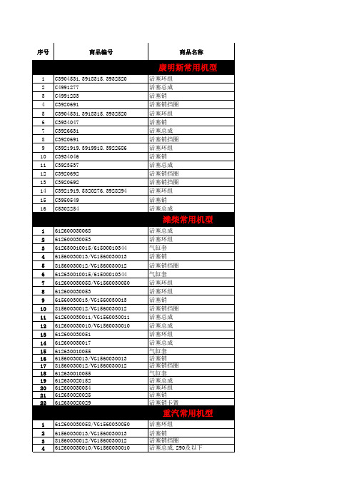
活塞总成.290以上 活塞总成.290以上升级版1 活塞总成.290以上升级版2 气缸套 活塞环组 活塞销 活塞销挡圈 活塞总成.290及以下 活塞总成.290以上 活塞总成.290以上升级版1 活塞总成.290以上升级版2 气缸套 活塞环组 活塞销 活塞销挡圈 活塞总成 气缸套 活塞环组 活塞销 活塞销挡圈 活塞总成 气缸套 活塞环组 活塞销 活塞销挡圈 活塞总成.290及以下 活塞总成.290以上 活塞总成.290以上升级版1 活塞总成.290以上升级版2 活塞总成.380 气缸套 活塞环组 活塞销 活塞销挡圈 活塞总成 气缸套
612600030011/VG1560030011 VG1560037011 VG1560037011A 612630010015/61500010344 VG1540030005 61560030013/VG1560030013 81560030012/VG1560030012 612600030010/VG1560030010 612600030011/VG1560030011 VG1560037011 VG1560037011A VG1540010006 VG1540030005 61560030013/VG1560030013 81560030012/VG1560030012 VG1540030004 VG1540010006 VG1540030005 61560030013/VG1560030013 81560030012/VG1560030012 VG1540030004 VG1540010006 612600030058/VG1560030050 61560030013/VG1560030013 81560030012/VG1560030012 612600030010/VG1560030010 612600030011/VG1560030011 VG1560037011 VG1560037011A VG1560030004 VG1540010006 VG1246030020 VG1246030002 VG1246030003 VG1246030001 VG1246010028
ROTAN CHD Pumps CHD service 说明书

CHD service manualROTAN CHD PumpsAnnex to Manual T1456DESMI Pumping Technology A/S Tagholm 1 – DK-9400 Nørresundby – DanmarkTel.: +45 96 32 81 11Fax: +45 98 17 54 99E-mail: ***************Internet: T1507UK-V.2.01. INTRODUCTIONS .................................................................................................................................... ‐ 2 ‐2. BEFORE START‐UP .................................................................................................................................. ‐ 7 ‐3. MAINTENANCE ..................................................................................................................................... ‐ 10 ‐4. REPLACEMENT OF SOFT PACKING RINGS .............................................................................................. ‐ 11 ‐5. REPLACEMENT OF LIP SEAL ................................................................................................................... ‐ 12 ‐6. INSPECTION OF IDLER PIN/BUSHING ..................................................................................................... ‐ 14 ‐7. INSPECTION/ADJUSTMENT OF AXIAL CLEARANCE ................................................................................. ‐ 16 ‐8. SPARE PARTS LIST ................................................................................................................................. ‐ 17 ‐9. ASSEMBLY DRAWINGS ......................................................................................................................... ‐ 18 ‐10. SERVICE CENTRES – DENMARK ......................................................................................................... ‐ 21 ‐11. SUBSIDIARY COMPANIES – DESMI PUMPING TECHNOLOGY A/S ....................................................... ‐ 22 ‐ Illustrations in this manual are only used to demonstrate the different working procedures. To a degree they are dependent on the size of the pump as there are different model constructions used for different applicationsWhen ordering spare parts the following information must be provided:- The pump serial number- The pump SX number- The spare part Position numberThe above information can be found on the pump flanges or the pump’s nameplate1. IntroductionsThis service manual only contains information about startup, service and maintains of Rotan CHD pumps.For general information about Rotan pumps please refer to manual T1456Rotan pumps are designed for pumping media with high viscosity such as chocolate, Cocoa Mass , Cocoa Butter, sugar powder etc. The Pump are equipped with heating jacket on the front and rear end. The Rotor, Idler and idler bushing are with special clearances.The Rotan CHD pumps are not Pressure or flow tested from the factory.The front cover and rear cover is pressure tested separately.CHD pumps are preserved with vegetable oil.Rotan CHD pumps are not approved for pumping foods requiring FDA and 3 A approval.DESMI Pumping Technology A/SDESMI Pumping Technology A/SEC Declaration of ConformityThe Machinery Directive 2006/42/ECManufacturer: DESMI Pumping Technology A/SAddress: Tagholm 1, DK-9400 Nørresundby, Denmark Tel.: +45 96 32 81 11 E-mail:***************DESMI Pumping Technology A/S hereby declares that the product in question has been produced in accordance with the following essential health and safety requirements of the Machinery Directive 2006/42/EC Annex I.Product: ROTAN pumps complete with motor Type: HD, CD, PD, GP, CC, ED(MD) Serial No: From 10000-xx-xx to 999999-xx-xxThe following harmonized standards have been applied:EN 809 + A1/AC:2010 Pumps and pump units for liquids DS/EN 12162 + A1:2009 Procedures for hydrostatic testing of liquid pumpsNørresundby 2015Claus Dietz Hansen Technical DirectorDESMI Pumping Technology A/SDESMI Pumping Technology A/SDeclaration of Incorporation”Manufacturer: DESMI Pumping Technology A/S Address: Tagholm 1, DK-9400 Nørresundby, Denmark. Tel.: +45 96 32 81 11 E-mail: ***************Product: ROTAN pumps Type: HD, CD, PD, GP, CC, ED(MD) Serial No: From 10000-xx-xx to 999999-xx-xxDESMI Pumping Technology A/S hereby declares that the product in question has been produced in accordance with the following essential health and safety requirements of the Machinery Directive 2006/42/EC Annex I:The following harmonized standards have been applied:EN 809:2002 + AC – Pumps and pump units for liquidsEN 12162 + A1:2009 – Procedures for hydrostatic testing of liquid pumpsThe pump must not be put into service until the final machinery into which the pump has been incorporated into, is declared in conformity with the provisions of the machinery directive 2006/42/EC.Nørresundby 2015Claus Dietz Hansen Technical DirectorDESMI Pumping Technology A/SDESMI Pumping Technology A/SEC Declaration of ConformityATEX – 94/9/ECManufacturer: DESMI Pumping Technology A/S Address: Tagholm 1, DK-9400 Nørresundby, Denmark. Tel.: +45 96 32 81 11 E-mail: ***************Product: ROTAN pumps Type: HD, CD, PD, GP, CC, ED(MD) which are marked: II category 2 or 3, ”c” X and with temperature class andinstalled and applied in conformity with DESMI Pumping Technology A/S’ user manualThe entire user manual must be read thoroughly before a ROTAN ATEX pump is installed and put into useD E S M I P u m p i n g T e c h n o l o g y A /S h e r e b y d e c l a r e s t h a t t h e p r o d u c t i n q u e s t i o n h a s b e e n p r o d u c e d i n a c c o r d a n c e w i t h A T E X D i r e c t i v e 94/9/E C .T h e f o l l o w i n g h a r m o n i s e d s t a n d a r d s h a v e b e e n a p p l i e d : E N 13463-1:2009 E N 13463-5:2011T h e p r o d u c t i s d e s i g n e d f o r u s e w h e n c o n n e c t e d t o a n e l e c t r i c m o t o r , w i t h t h e a i m o f c r e a t i n g a j o i n t m a c h i n e . T h e c o n f o r m i t y a l s o a p p l i e s t o c o m p l e t e p u m p s w i t h m o t o r i f , a c c o r d i n g t o t h e m a n u f a c t u r e r , t h e m o t o r c o n f o r m s t o a c o r r e s p o n d i n g c a t e g o r y a n d t e m p e r a t u r e c l a s s a n d h a s b e e n f i t t e d i n c o n f o r m i t y w i t h D E S M I P u m p i n g T e c h n o l o g y A /S ’ u s e r g u i d e .If DESMI Pumping Technology A/S supplies pump and electric motor connected, the EC Declaration of Conformity and user manual for the electric motor will be attached.Nørresundby 2015Claus Dietz Hansen Technical DirectorDESMI Pumping Technology A/SDESMI Pumping Technology A/SDESMI Pumping Technology A/S2. Before start-upRotan CHD pumps are preserved with vegetable oil at the factory, If this oil is not compatible with the media that is pumped, the pump should be cleaned before startup.Rotan CHD pumps is fitted with a special shaft seal, and may not be mistaken for a standard soft shaft packing (see Figure 1)The main bushing and the soft packing rings are not lubricated from the factory.The main bushing and the soft packing is to be lubricated before startup. Make sure that the lubrication media is compatible with the media that’s is pumpedWhen lubricating the main bushing and the soft packing, the lubrication pressure must notexceed 20 bar / 290 psi. If the lubrication pressure exceeds this, there is a risk of damaging the Lip seal and the packing gland.Prelubrication amounts of main bearingPrelubrication amount for main bearingPump sizeHD - CDGrease in cm3 (cubic centimeters)33 5,0 41 7,5 51/66 25,5 81/101 27,0 126 24,0 151 28,0 152 42,0Remember to close the pet cock valve after lubricationFigure 1. Shows Construction of CHD shaft seal DESMI Pumping Technology A/SDESMI Pumping Technology A/SBefore starting the pump, check:∙ That the main bushing and soft packing is lubricated with Food grade grease That the pump is correctly aligned with the gear and motor. See chapter: “Aligning the ∙ pump and gear/motor” Main manual T1456∙ That the pump is heated, to secure a free rotation of the shaft∙ That the ball bearings maximum service life is observed See main manual T1456 ∙ That all isolating valves in the suction and pressure pipe are fully open, to avoid thepressure being too high, and the pump running dry ∙ That there is no coagulated liquid in the pump or pipe system, after last operation,that can cause blockage or breakdown ∙ That all necessary monitoring and safety system are connected and adjustedaccording to the operation conditionsAfter starting the pump, check:∙ That the pump is drawing the liquid∙ That there are no signs of cavitation i.e. excessive noise and or vibration ∙ That the speed is correct∙ That the direction of rotation is correct ∙ That there is no leakage from the pump ∙ That the shaft seal not leaking(the shaft seal on a CHD pump is a isolated construction and there for leak free) ∙That the operation pressure is correct∙ That the pressure in the heating jackets not exceeds 10 bar∙ That the magnetic clutch (type ED) is not slipping and then causing an inadequateflow. And that the temperature in the magnetic clutch does not exceed the permitted l ∙ That the power consumption is correct∙ That all surveillance equipment is working correctly∙ That any pressurized water pipes, Heating/cooling and lubricating systems, etc. are working correctly3. MaintenanceNormal Maintenance of the Rotan CHD pumps will typically include the following.1. Lubrication of the soft shaft seal and main bushing2. Inspection of leakage from the lip seal (the lip seal is leak free)3. Inspection of wear on the idler pin and idler bushingThe implementation of the above mentioned maintenance points, can vary a lot, depending of the operations conditions.DESMI Pumping Technology A/S recommend that the soft packing and main bushing is lubricated at an 8 hour intervals (see diagram below) it is important that the lubrication interval is adjusted to the operations conditions, so that the media is kept away from the main bushing and lip seal. Automatic grease pots may be fittedAfter roughly one month operation it is recommended that the front cover is removed for inspection for wear on the idler pin/bushing, and disassembly of the rear end for inspection of wear on the shaft – main bushing and the lip seal if there is traces of the pumped media in the main bushing, it is recommended that the lubrication interval is adjusted.The operating conditions, can be very different, so it is recommended that the company work out a procedure for servicing the pumps (lubrications interval, inspection of wear) that is adjusted to the pump operation conditions.Lubrication of slide bearings CHDFat quantity in gramsPump type: HD – CD – ED Relubrication intervalin hours Main bearing338 hours 141 151 1,566 1,581 2101 2,5126 4151 6152 10DESMI Pumping Technology A/SDESMI Pumping Technology A/S4. Replacement of soft packing ringsThe Rotan CHD pumps are constructed with a split packing gland follower, which allows the main bearing bushing to be pulled out of the pump and the soft packing rings can be replaced.Remove the nut (pos. BE) and pull back the packing gland (pos. BB) along with the mainbushing (pos. BC). Remove the bolts in the packing gland (pos. EJ), pull the main bushing as far back as possible. Gently Use a Flexible Packing Extractor for pulling out the soft packing rings (poss. CJ). Clean the area before, replacing them with new ones.If the nuts (pos. BE) are tightened too hard it can result in high heat generation, and poor lubrication of the soft packing rings. Under these conditions there is a very high risk of damaging the soft packing rings and the shaft5. Replacement of Lip sealWhen replacing the Lip seal (pos. EG) in the main bushingThe rear end is to be dismantled. See Array figure 2Rotan pumps are constructed with a backpull out systemthat allows the pump casing to remain inthe pipe systemWhilst the rear end is removed as show infigure. aRemove the bolts pos. FRemove the rear end.The rear end is now ready to bedismantled.The Lip seal pos. EG. Can be replaced.Use the proper tools to remove the ballbearing.Clean all components before assembling them.The rear end is now ready to be mounted in the pump casing, Remember to check/adjust the axial clearance see chapter “Inspection/adjustment of axial clearance”.Remember to lubricate the soft packing and main bushing before starting up the pump.Figure. aDESMI Pumping Technology A/SDESMI Pumping Technology A/SFigure. 2 Exploded view of rear endDESMI Pumping Technology A/S6. Inspection of Idler pin/BushingRemove the bolts pos. E. and gently pull out the front cover including the Heating jackets (figure. 3)Be careful that the idler doesn’t fall down when removing the front coverPump size 81 to 201 use proper lifting equipment.Clean the front cover, and inspect the idler pin Poss. AC For Wear (figure. 4)Clean the idler busing pos. AD and inspect it for wear (figure. 5) See figure 7 for measuring wear on idler pin and busingClean the packing surface on the front cover and pump before mounting the front cover on the pump againFrom the size 81 to 152 the Idler is manufactured with a tapered surface between the teeth, the idler is placed on the idler pin with the tapered surface pointing against the front cover. See Figure 6Figure. 3 Removing of front cover Figure.4 Front coverFigure. 6Figure. 5 IdlerDESMI Pumping Technology A/SMeasuring of wearMeasure the diameter on the idler pin and the diameter on the idler bushing the clearance must not exceed measurements stated in the above table (Figure 8)Pump Size RecommendedClearance after wearD+D max(mm)41 1,5 51 1,7 66 1,7 81 1,7 101 1,7 126 1,8 151 1,8 152 1,8Figure. 7Figure. 8DESMI Pumping Technology A/S7. Inspection/adjustment of axial clearanceThe axial clearance is the distance between rotor and front cover Type ED: Adjustments screws pos. E/NMThe adjustments screws is to be turned in pairs and in the same angle. Figure:11 Show the axial clearance in mm for the different pump sizes.** Pumps in stainless steel is to be adjusted with 0,10mm larger clearance than stated above. Pumps in stainless steel is recognized by a 3 in the pump code example: CD26EFCHD-3M22BAxial clearence CHDPump size26/33 41 51/66 81/101 126/151 152 CHD*Min.0,20 0,250,20 0,300,30 0,400,40 0,500,60 0,750,70 0,90Max.Stainless pumps**Is adjusted with 0,10mm larger clearance than stated aboveIdler°8. Spare parts List Position numberA = Pump casingB = GasketC = GasketD = BoltE = BoltF = BoltG = Pipe plugJ = Drive screw S = Blind cover AA = Front cover AB = IdlerAC = Idler pinAD = Idler bushing AF = GasketAJ = Heating jacket AK = BoltAL = Pipe plugBA = Rear coverBB = Packing glandBC = Main bearing bushing BD = Stud boltBE = NutBF = WasherBG = Pipe plugBH = Pipe plugBJ = BoltBK = Pipe plugBL = Lubrication sign CHD BU = RotorBV = ShaftBY = Ball bearing nutBZ = Ball bearing lock ring CA = KeyCB = KeyCE = Snap ringCJ = Packing coilCQ = BracketCR = Bearing coverCS = Bearing coverCT = BoltCU = Ball bearingEF = O-ringEG = Seal ringEJ = Bolt EK = NippleEK = NippleEL = BibcockEM = lubricating nippleER = Support ringFP = Welding sleeveHE = BoltHG = Cover plate for idler pin HH = ScrewHE = BoltHF = WasherHR = GasketJL = GasketKM = Spacer ringWhen ordering spare parts the following information must be provided:- The pumps serial number- The pumps SX number- The spare part Possession numberThe above information can be found on the pump flanges or the pump’s nameplateDESMI Pumping Technology A/SDESMI Pumping Technology A/S9. Assembly drawingsAssembly drawings for Rotan CHD pumps Size 33 to 201DESMI Pumping Technology A/SDESMI Pumping Technology A/S10. Service centres – DenmarkService center - DenmarkNøresundby Tagholm 1DK-9400 Nørresundby Tel: +45 70236363 Fax: +45 9817 5499 KoldingAlbuen 18 CDK-6000 Kolding Tel: +45 7023 6363 Fax: +45 75 58 34 65Århus Lilleringvej 20DK-8462 Harlev J Tel: +45 7023 6363 Fax: +45 8694 2292 Hvidovre Stamholmen 173 DK-2650 Hvidovre Tel: +45 70236363 Fax: +45 3677 3399OdenseHestehaven 61DK-5260 Odense STel: +45 70236363Fax: +45 6595 7565DESMI Pumping Technology A/S11. Subsidiary companies – DESMI Pumping Technology A/SSubsidiary companies – DESMI Pumping Technology A/SDESMI Denmark A/SAddress: Tagholm 1,DK-9400 Nørresundby DenmarkTel: +45 7244 0250Fax: +45 9817 5499 DESMI Inc.Address: 4021 Holland Blvd, Chesapeake Virginia 23323, USATel.: +1 757 857 7041Fax.: +1 757 857 6989DESMI Contracting A/SAddress: Tagholm 1,DK-9400 Nørresundby DenmarkTel.: +45 96 32 81 11Fax: +45 98 17 54 99 DESMI Pumping Technology (Suzhou) Co., Ltd Address: No 740 Fengting avenue,Weiting Sub-District 215122 SIP Suzhou, ChinaTel.: +86 512 6274 0400Fax.: +86 512 6274 0418DESMI GmbHAddress: An der Reitbahn 1521218 Seevetal, Germany Tel.: +49 40 7519 847Fax: +49 40 7522 040 DESMI KoreaAddress: 905 ,Western Tower I, Janghang-dong 867, Ilsandong-gu, Goyang,Gyeonggi 410-838, KoreaTel.: +82 31 931 5701Fax.: +82 31 931 5702DESMI Ltd.Address: “Norman House” Rosevale Business Park, Parkhouse industrialEstate (West) Newcasle, StaffordshireST5 7UB, EnglandTel.: +44 1782 566 900Fax.: +44 1782 563 666 DESMI Singapore Pte.LtdAddress: No. 8 Kaki Bukit Road 2,Ruby Warehouse ComplexUnit no: # 02-16 Singapore 417841 Tel.: +65 6748 2481Fax.: +65 6747 6172DESMI B.VAddress: Texasdreef 7,3565 CL Utrech NetherlandsTel.: +31 3026 610 024Fax.: +31 302 623 314 DESMI IndiaAddress: 413,Adity Trade CentreAmeerpet, Hyderabad - 500016 Tel.: +91 9949339054DESMI Norge ASAddress: Vigevejen 46,4633 Kristiansand S, Norway Tel.: +47 38 122 180Fax.: +47 38 122 181 DESMI AfricaAddress: Plot No.1848 Yarht Club RoadMsasani Peninsular, Dar esSalaam,TanzaniaTel. +255 769756919DESMI Pumping Technology A/SDESMI Pumping Technology A/S。
1734系列数字电流输入模块说明书
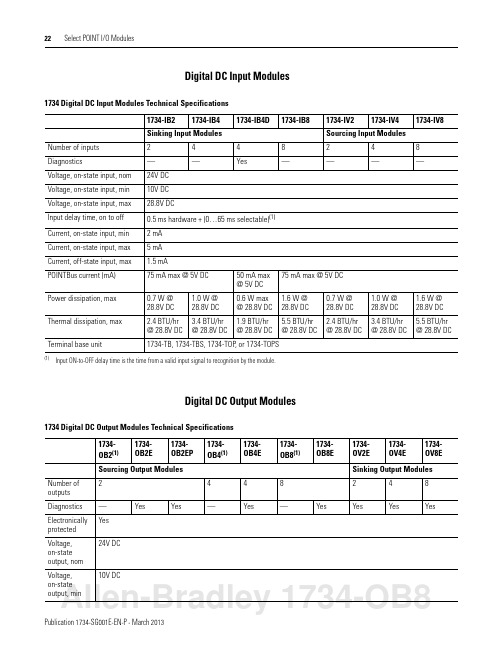
22 Select POINT I/O ModulesDigital DC Input ModulesDigital DC Output Modules1734 Digital DC Input Modules Technical Specifications1734-IB21734-IB41734-IB4D 1734-IB81734-IV21734-IV41734-IV8Sinking Input Modules Sourcing Input ModulesNumber of inputs 2448248Diagnostics——Yes————Voltage, on-state input, nom 24V DC Voltage, on-state input, min 10V DC Voltage, on-state input, max 28.8V DCInput delay time, on to off 0.5 ms hardware + (0…65 ms selectable)(1)Current, on-state input, min 2 mA Current, on-state input, max 5 mA Current, off-state input, max 1.5 mAPOINTBus current (mA)75 mA max @ 5V DC 50 mA max @ 5V DC 75 mA max @ 5V DC Power dissipation, max 0.7 W @ 28.8V DC1.0 W @ 28.8V DC0.6 W max @ 28.8V DC 1.6 W @ 28.8V DC 0.7 W @ 28.8V DC 1.0 W @ 28.8V DC 1.6 W @ 28.8V DC Thermal dissipation, max 2.4 BTU/hr @ 28.8V DC 3.4 BTU/hr @ 28.8V DC1.9 BTU/hr @ 28.8V DC5.5 BTU/hr @ 28.8V DC2.4 BTU/hr @ 28.8V DC3.4 BTU/hr @ 28.8V DC5.5 BTU/hr @ 28.8V DCTerminal base unit1734-TB, 1734-TBS, 1734-TOP , or 1734-TOPS(1)Input ON-to-OFF delay time is the time from a valid input signal to recognition by the module.1734 Digital DC Output Modules Technical Specifications1734-OB2(1)1734-OB2E1734-OB2EP1734-OB4(1)1734-OB4E1734-OB8(1)1734-OB8E1734-OV2E1734-OV4E1734-OV8ESourcing Output ModulesSinking Output Modules Number of outputs 2448248Diagnostics —YesYes—Yes—Yes YesYesYesElectronically protected Yes Voltage, on-state output, nom 24V DCVoltage, on-state output, min10V DCAllen-Bradley 1734-OB8Select POINT I/O Modules 23Digital Contact ModulesVoltage, on-state output, max28.8V DCOutput current rating, max 2.0 A per module, 1.0A per channel4.0 A per module, 2.0 A per channel3.0 A per module, 1.0 A per channel2.0 A max per module, 1.0 A per output3.0 A per module, 1.0 A per output 3.0 A per module, 1.0 A per channelPOINTBus current (mA) 75Power dissipation, max ************3.4 W @ 28.8V DC************************0.8 W max @ 28.8V DC 1.2 W max @ 28.8V DC 2.0 W max @ 28.8V DC Thermal dissipation, max2.7BTU/********DC 11.6 BTU/hr @ 28.8V DC4.1BTU/********DC 6.8BTU/********DC2.7 BTU/hr @ 28.8V DC 4.1 BTU/hr @ 28.8V DC 6.8BTU/hr @ 28.8V DCTerminal base unit1734-TB, 1734-TBS, 1734-TOP , or 1734-TOPS (1)Non-diagnostic, standard output modules.1734 Digital DC Output Modules Technical Specifications1734-OB2(1)1734-OB2E1734-OB2EP1734-OB4(1)1734-OB4E1734-OB8(1)1734-OB8E1734-OV2E1734-OV4E1734-OV8E1734 Digital Contact Modules Technical Specifications1734-OW21734-OW4 1734-OX2Number of outputs2 N.O. relays4 N.O. relays2 Form C (N.O./N.C.) relays, isolated Output delay time, on to off, max 26 ms (1)10 ms (1)Contact resistance, initial 30 m ΩLeakage current, off-state output, max1.2 mA and bleed resistor through snubber circuit @ 240V AC 1.2 mA and bleed resistor through snubber circuit @ 240V AC POINTBus current (mA) 80 100Power dissipation, max 0.5 W Thermal dissipation, max 1.7 BTU/hrTerminal base unit1734-TB, 1734-TBS, 1734-TOP , or 1734-TOPS(1)Time from valid output off signal to relay deenergization by module.Mounting Requirements 63 Approximate Mounting DimensionsPOINT I/O with 1734-PDN Mounting DimensionsIMPORTANT When mounting the 1734-IB8S, 1734-OB8S, and 1734-IE4S modules, ensure that there is 2in. of clearance space above thePOINT rail.Allen-Bradley 1734-OB8。
(OA自动化)GEPLC机组自动化装置编程使用说明书
DMP-300F型中小型水电站触摸式机组自动化屏(GE Fanuc PLC+Pro-face 或Weintek触摸屏) 编程使用说明书文件编号:__________________版本号:__________________发放编号:__________________持册人:__________________长沙华能自控集团有限公司目录一、GE FANUC PLC介绍 (1)(一)、GE FANUC 90-30系列PLC介绍 (1)1、机架底板 (1)⏹机架底板外形 (1)⏹机架底板型号 (2)2、电源模块 (2)⏹外形 (2)⏹电源模块指示器具体含义 (2)⏹电源模块型号及性能 (3)⏹使用注意 (3)⏹电源模块上的通信端口 (3)⏹电源模块上的通信端口RS422接线图: (3)3、CPU模块 (4)⏹350型CPU(IC693CPU350)外形 (4)⏹350型CPU(IC693CPU350)性能参数 (4)4、通信模块 (5)⏹串口通信模块(IC693CMM311) (5)⏹以太网通信模块(IC693CMM321) (6)⏹可编程协处理器模块(IC693PCM301或IC693PCM311) (6)⏹现场总线模块 (7)Profibus-DP总线模块 (7)DeviceNet总线模块 (8)机组自动化现场总线配置原则 (8)5、AD模块 (9)普通AD输入模块 (9)普通AD混合模块 (11)热电阻AD模块 (12)6、开关量输入模块 (13)7、开关量输出模块 (14)(二)、GE FANUC VERSAMAX系列PLC介绍 (15)1、系统基本构成 (16)2、CPU模块 (17)⏹外形 (17)⏹特性 (17)3、网络接口单元(NIU) (18)⏹Profibus NIU(IC200PBI001) (18)⏹DeviceNet NIU(IC200DBI001) (19)4、通信模块 (19)⏹Profibus-DP网从模块(IC200BEM002) (19)⏹DeviceNet网控制模块(IC200BEM103) (20)5、AD模块 (21)普通AD输入模块 (21)普通AD混合模块 (22)IC200ALG620(四通道RTD热电阻AD模块,分辨率16位) (23)6、开关量输入模块 (24)IC200MDL640(24VDC 16点[2个8点组]的正/负逻辑输入模块) (24)IC200MDL650(24VDC 32点[4个8点组]的正/负逻辑输入模块) (24)7、开关量输出模块 (25)IC200MDL730(24VDC 正逻辑的8点输出模块,每点2.0A[1组8个点]) (25)IC200MDL740(24VDC 正逻辑的16点输出模块,每点0.5A[1组16个点]) (25)IC200MDL750(24VDC 正逻辑的32点输出模块,每点0.5A[2组16个点]) (26)IC200MDL930(2.0A每点均隔离的8点继电器输出) (26)IC200MDL940(2.0A每点均隔离的16点继电器输出) (26)二、GE FANUC PLC机组自动化常用指令介绍 (27)(一)、梯形图指令 (27)1、触点 (27)⏹常开触点 (27)⏹常闭触点 (27)⏹一些系统触点的含义(只能做触点用,不能做线圈用) (27)2、线圈 (28)⏹常开线圈 (28)⏹求反线圈 (29)⏹保持线圈 (29)⏹非保持线圈 (29)⏹正向变换线圈 (29)⏹反向变换线圈 (29)⏹置位线圈 (30)⏹复位线圈 (30)⏹保持置位线圈 (30)⏹保持复位线圈 (30)⏹链回路 (31)⏹特别注意 (31)(二)、定时器和计数器指令 (31)1、定时器和计数器指令所需的数据 (31)2、简单接通延时定时器(TMR) (31)3、保持接通延时定时器(ONDTR) (32)4、断开延时定时器(OFDT) (33)5、加计数器(UPCTR) (34)6、减计数器(DNCTR) (34)(三)、比较(关系运算)指令 (35)1、普通比较指令(EQ、NE、GT、GE、LT、LE) (35)2、区间比较指令(R ANGE) (36)(四)、数学运算指令 (36)1、四则运算和求余指令(ADD、SUB、MUL、DIV、MOD) (37)2、平方根指令(SQRT) (38)3、三角函数指令(SIN、COS、TAN、ASIN、ACOS、ATAN) (38)4、特别说明 (39)(五)、位操作指令 (39)1、与(AND)和或(OR)指令 (39)2、异或(XOR)指令 (40)3、求非(NOT)指令 (41)4、左移位(SHIFTL)、右移位(SHIFTR)指令 (41)5、左循环移位(ROL)、右循环移位(ROR)指令 (42)6、位测试(BIT_TEST指令) (43)7、位置位(BIT_SET指令)和位清零(BIT_CLR)指令 (44)8、位定位指令(BIT_POS)指令 (44)9、屏蔽比较(MASK_COMP_WORD、MASK_COMP_DWORD)指令 (45)(六)、数据传送指令 (46)1、数据移动(MOVE_**,其中**为数据类型)指令 (46)2、块移动(BLKMOV_**,其中**为数据类型)指令 (47)3、块清零(BLKCLR_**,其中**为数据类型)指令 (48)4、移位寄存器(SHFR_**,其中**为数据类型)指令 (48)(七)、数据表格指令 (49)1、数据移动(ARRAY_MOVE_**,其中**为数据类型)指令 (49)2、数据搜索(SEARCH_$$_**_**,其中$$为搜索关系,**为数据类型)指令 (50)(八)、数据转换指令 (51)1、变换成BCD4(INT_TO_BCD4、UINT_TO_BCD4)指令 (51)2、其他数据转换指令 (52)3、特别说明 (52)(九)、控制指令 (52)1、调用子程序(CALL)指令: (53)2、服务请求(SVC_REQ)指令: (53)3、程序结束(END)指令: (55)三、GE FANUC PLC编程软件操作 (55)(一)、CIMPLICITY MACHINE EDITION 5.0 (55)1、CIMPLICITY M ACHINE E DITION简介 (56)2、创建、编辑工程 (56)3、工具栏 (57)4、变量定义 (58)5、编写程序 (59)(二)、VERSAPRO 2.03 (63)四、机组自动化装置中硬件配置 (63)(一)、CPU模块配置 (63)1.IC693CPU350(90-30系列)配置 (63)2.IC200CPU001(V ERSA M AX系列)配置 (64)3.IC200CPUE05(V ERSA M AX系列)带以太网配置 (65)(二)、90-30系列以太网通信模块(IC693CMM321)设置 (66)(三)、90-30系列串口通信模块(IC693CMM311)设置 (66)(四)、90-30系列可编程协处理器(IC693PCM301、IC693PCM311)设置 (67)(五)、AD模块(以IC693ALG223为例)设置 (67)(六)、开关量输入模块(以IC693MDL655为例)设置 (68)(七)、开关量输出模块(以IC693MDL753为例)设置 (68)(八)、PROFIBUS-DP现场总线通信设置 (69)1.主站设置(IC693PBM200设置) (69)2.从站设置(IC200BEM002设置) (71)(九)、DEVICENET现场总线通信设置 (72)1.主站设置(IC693DNM200设置) (72)2.从站设置(CPM1A-DRT21设置) (73)五、机组自动化装置中程序结构 (73)六、机组自动化装置与DMP保护器通信程序 (74)1.程序代码: (74)2.使用TERMF下装程序到可编程协处理模块(IC693PCM301) (87)七、机组自动化装置寄存器分配 (87)(一)、%R:内部数据寄存器 (87)(二)、%I:输入位寄存器 (91)(三)、%Q:输出位寄存器 (91)(四)、%M:内部位寄存器 (91)(五)、%AI:输入AD采样寄存器 (93)(六)、%AQ:DA模块寄存器 (93)八、台湾WEINTEK触摸屏连接GE FANUC PLC (93)九、PRO-FACE触摸屏连接GE FANUC PLC (94)(一)、慨述 (94)画面类型 (94)GP内部的存储器(LS)地址 (94)GP-Setup(初始化设置) (96)(二)、画面编辑器 (98)菜单 (98)Draw的应用 (99)Part的功能介绍 (99)Tag的功能介绍 (115)D-Script/Global-Script (123)(三)、工程管理器之其它编辑器和应用程序 (125)(四)、画面说明 (130)(五).OFF-LINE方式 (131)(六)、工程的传送、保护与模拟 (140)一、GE Fanuc PLC介绍目前根据市场的需要,公司新开发了一套基于美国通用公司GE Fanuc 90-30系列或者VersaMax系列PLC为控制核心的机组自动化装置。
Motorola 3.5 kHz 产品说明书
RVN4126 3.59100-386-9100-386/T DEVICERVN41772-CD2-3.5MCS/MTSRVN41821-CD2-3.5XTS3000/SABER PORTABLE YES RKN4046KHVN9085 3.51-20 R NO HLN9359 PROG. STAND RVN4057 3.532 X 8 CODEPLUG NO3080385B23 & 5880385B30 MDVN4965 3.59100-WS/T CONFIG KITRVN4053 3.5ASTRO DIGITAL INTERFACE NO3080385B23RVN41842-CD RKN4046A (Portable) 2-3.5ASTRO PORTABLE /MOBILE YES3080369B73 or0180300B10 (Mobile) RVN41831-CD3080369B732-3.5ASTRO SPECTRA MOBILE YES(Low / Mid Power)0180300B10 (High Power) RVN4185CD ASTRO SPECTRA PLUS MOBILE NO MANY OPTIONS; SEESERVICE BRIEF#SB-MO-0101RVN4186CD ASTRO SPECTRA PLUS MANY OPTIONS;MOBILE/PORTABLE COMB SEE SERVICE BRIEF#SB-MO-0101RVN4154 3.5ASTROTAC 3000 COMPAR.3080385B23RVN5003 3.5ASTROTAC COMPARATORS NO3080399E31 Adpt.5880385B34RVN4083 3.5BSC II NO FKN5836ARVN4171 3.5C200RVN4029 3.5CENTRACOM SERIES II NO VARIOUS-SEE MANUAL6881121E49RVN4112 3.5COMMAND PLUS NORVN4149 3.5COMTEGRA YES3082056X02HVN6053CD CT250, 450, 450LS YES AAPMKN4004RVN4079 3.5DESKTRAC CONVENTIONAL YES3080070N01RVN4093 3.5DESKTRAC TRUNKED YES3080070N01RVN4091 3.5DGT 9000 DESKSET YES0180358A22RVN4114 3.5GLOBAL POSITIONING SYS.NO RKN4021AHVN8177 3.5GM/GR300/GR500/GR400M10/M120/130YES3080070N01RVN4159 3.5GP60 SERIES YES PMLN4074AHVN9128 3.5GP300 & GP350RVN4152 3.5GP350 AVSRVN4150 3.5GTX YES HKN9857 (Portable)3080070N01(Mobile) HVN9025CD HT CDM/MTX/EX SERIES YES AARKN4083/AARKN4081RiblessAARKN4075RIBLESS NON-USA RKN4074RVN4098H 3.5HT1000/JT1000-VISAR YES3080371E46(VISAR CONV)RVN4151 3.5HT1000 AVSRVN4098 3.5HT1000/ VISAR CONV’L.YES RKN4035B (HT1000) HVN9084 3.5i750YES HLN-9102ARVN4156 3.5LCS/LTS 2000YES HKN9857(Portable)3080070N01(Mobile) RVN4087 3.5LORAN C LOC. RECV’R.NO RKN4021ARVN4135 3.5M100/M200,M110,M400,R100 includesHVN9173,9177,9646,9774YES3080070N01RVN4023 3.5MARATRAC YES3080070N01RVN4019 3.5MAXTRAC CONVENTIONAL YES3080070N01RVN4139 3.5MAXTRAC LS YES3080070N01RVN4043 3.5MAXTRAC TRK DUPLEX YES3080070N01RVN4178CD MC SERIES, MC2000/2500DDN6124AW/DB25 CONNECTORDDN6367AW/DB9 CONNECTOR RVN41751-CD Rib to MIC connector 1-3.5MCS2000 RKN4062BRVN41131-3.5MCS2000RVN4011 3.5MCX1000YES3000056M01RVN4063 3.5MCX1000 MARINE YES3000056M01RVN4117 3.5MDC/RDLAP DEVICESRVN4105 3.5MOBILE PROG. TOOLRVN4119 3.5MOBITEX DEVICESRVN4128 3.5MPT1327-1200 SERIES YES SEE MANUALRVN4025 3.5MSF5000/PURC/ANALOG YES0180355A30RVN4077 3.5MSF5000/10000FLD YES0180355A30RVN4017K 3.5MT 1000YES RTK4205CRVN4148 3.5MTR 2000YES3082056X02RVN4140 3.5MTRI 2000NORVN41761-CD MTS2000, MT2000*, MTX8000, MTX90001-3.5*programmed by DOS which is included in the RVN4176RVN4131 3.5MTVA CODE PLUG FIXRVN4142 3.5MTVA DOCTOR YES3080070N01RVN4131 3.5MTVA3.EXERVN4013 3.5MTX800 & MTX800S YES RTK4205CRVN4097 1-CD MTX8000/MTX9000,MTS2000,MT2000*,* programmed by DOS which is included in the RVN4176HVN9067CD MTX850/MTX8250MTX950,MTX925RVN4138 3.5MTX-LS YES RKN4035DRVN4035 3.5MX 1000YES RTK4203CRVN4073 3.5MX 800YES RKN4006BHVN9395 P100, P200 LB, P50+, P210, P500, PR3000RVN4134 3.5P100 (HVN9175)P200 LB (HVN9794)P50+ (HVN9395)P210 (HVN9763)P500 (HVN9941)PR3000 (HVN9586)YES RTK4205HVN9852 3.5P110YES HKN9755A/REX1143 HVN9262 3.5P200 UHF/VHF YES RTK4205RVN4129 3.5PDT220YVN4051 3.5PORTABLE REPEATER Portable rptr.P1820/P1821AXRVN4061C 3.5PP 1000/500NO3080385B23 & 5880385B30 RVN5002 3.5QUANTAR/QUANTRO NO3O80369E31RVN4135 3.5R100 (HVN9177)M100/M200/M110/M400YES0180358A52RVN4146 3.5RPM500/660RVN4002 3.5SABER YES RTK4203CRVN4131 3.5SETTLET.EXEHVN9007 3.5SM50 & SM120YESRVN4039 3.5SMART STATUS YES FKN5825AHVN9054 3.5SOFTWARE R03.2 P1225YES3080070N01HVN9001 3.5SOFTWARE R05.00.00 1225LS YES HLN9359AHVN9012 3.5SP50RVN4001N 3.5SPECTRA YES3080369B73 (STANDARD)0180300B10 (HIGH POWER) RVN4099 3.5SPECTRA RAILROAD YES3080369B73RVN4110 3.5STATION ACCESS MODULE NO3080369E31RVN4089A 3.5STX TRANSIT YES0180357A54RVN4051 3.5SYSTEMS SABER YES RTK4203BRVN4075 3.5T5600/T5620 SERIES NO3080385B23HVN9060CD TC3000, TS3000, TR3000RVN4123 3.5VISAR PRIVACY PLUS YES3080371E46FVN4333 3.5VRM 100 TOOLBOX FKN4486A CABLE &ADAPTORRVN4133 3.5VRM 500/600/650/850NORVN4181CD XTS 2500/5000 PORTABLES RKN4105A/RKN4106A RVN41002- 3.5XTS3000 ASTRO PORTABLE/MOBILERVN4170 3.5XTS3500YES RKN4035DRIB SET UPRLN4008E RADIO INTERFACE BOX (RIB)0180357A57RIB AC POWER PACK 120V0180358A56RIB AC POWER PACK 220V3080369B71IBM TO RIB CABLE (25 PIN) (USE WITH XT & PS2)3080369B72IBM TO RIB CABLE (9 PIN)RLN443825 PIN (F) TO 9 PIN (M) ADAPTOR (USE W/3080369B72 FOR AT APPLICATION) 5880385B308 PIN MODULAR TO 25 PIN ”D” ADAPTOR (FOR T5600 ONLY)0180359A29DUPLEX ADAPTOR (MOSTAR/TRAXAR TRNK’D ONLY)Item Disk Radio RIB Cable Number Size Product Required Number Item Disk Radio RIB Cable Number Size Product Required NumberUtilizing your personal computer, Radio Service Software (RSS)/Customer Programming Software (CPS)/CustomerConfiguration Software (CCS) enables you to add or reprogram features/parameters as your requirements change. RSS/CPS/CCS is compatible with IBM XT, AT, PS/2 models 30, 50, 60 and 80.Requires 640K RAM. DOS 3.1 or later. Consult the RSS users guide for the computer configuration and DOS requirements. (ForHT1000, MT/MTS2000, MTX838/8000/9000, Visar and some newer products —IBM model 386, 4 MEG RAM and DOS 5.0 or higher are recommended.) A Radio Interface Box (RIB) may be required as well as the appropriate cables. The RIB and cables must be ordered separately.Licensing:A license is required before a software (RVN) order is placed. The software license is site specific (customer number and ultimate destination tag). All sites/locations must purchase their own software.Be sure to place subsequent orders using the original customer number and ship-to-tag or other licensed sites; ordering software without a licensed customer number and ultimate tag may result in unnecessary delays. To obtain a no charge license agreement kit, order RPX4719. To place an order in the U.S. call 1-800-422-4210. Outside the U.S., FAX 847-576-3023.Subscription Program:The purchase of Radio ServiceSoftware/Customer Programming/Customer ConfigurationSoftware (RVN & HVN kits) entitles the buyer/subscriber to three years of free upgrades. At the end of these three years, the sub-scriber must purchase the same Radio Service Software kit to receive an additional three years of free upgrades. If the sub-scriber does not elect to purchase the same Radio Service Software kit, no upgrades will be sent. Annually a subscription status report is mailed to inform subscribers of the RSS/CPS/CCS items on our database and their expiration dates.Notes:1)A subscription service is offered on “RVN”-Radio Service Software/Customer Programming/Customer Configuration Software kits only.2)“RVN” software must only be procured through Radio Products and Services Division (RPSD). Software not procured through the RPSD will not be recorded on the subscription database; upgrades will not be mailed.3)Upgrades are mailed to the original buyer (customer number & ultimate tag).4)SP software is available through the radio product groups.The Motorola General Radio Service Software Agreement is now available on Motorola Online. If you need assistance please feel free to submit a “Contact Us” or call 800-422-4210.SMART RIB SET UPRLN1015D SMART RIB0180302E27 AC POWER PACK 120V 2580373E86 AC POWER PACK 220V3080390B49SMARTRIB CABLE (9 PIN (F) TO 9 PIN (M) (USE WITH AT)3080390B48SMARTRIB CABLE (25 PIN (F) TO 9 PIN (M) (USE WITH XT)RLN4488ASMART RIB BATTERY PACKWIRELESS DATA GROUP PRODUTS SOFTWARERVN4126 3.59100-386/9100T DEVICES MDVN4965 3.59100-WS/T CONFIG’TN RVN41173.5MDC/RDLAP DEVICESPAGING PRODUCTS MANUALS6881011B54 3.5ADVISOR6881029B90 3.5ADVISOR ELITE 6881023B20 3.5ADVISOR GOLD 6881020B35 3.5ADVISOR PRO FLX 6881032B30 3.5BR8506881032B30 3.5LS3506881032B30 3.5LS5506881032B30 3.5LS7506881033B10 3.5LS9506881035B20 3.5MINITOR III8262947A15 3.5PAGEWRITER 20008262947A15 3.5PAGEWRITER 2000X 6881028B10 3.5TALKABOUT T3406881029B35 3.5TIMEPORT P7308262947A15 3.5TIMEPORT P930NLN3548BUNIVERSAL INTERFACE KITItem Disk Radio NumberSize Product。
Allwinner R8 Datasheet

REVISION HISTORYDECLARATIONTABLE OF CONTENTS5.3. DC Electrical Characteristics2.6.Memory Subsystem&Touch G-SENSORSPI1_CLK UART3_RX42 DDR3_D743 VCC3_DRAM79 AGND80 VRPSDC0_CMD 111PF3PE9 CSI_D6LCD_D10 141PD10PC19 163 VCC4function 0);3)Type: signal directionPC7 Input PC8 InputPE4 Input PE5 InputSignal Name DescriptionOthersVRP Reference voltageV IH High-Level Input Voltage V IL Low-Level Input VoltageFigure 5-1. Power Up Sequence5.5.2.Power Up Reset Sequence RequirementsThe device has a system reset signal to reset the board. When asserted, the following steps give an example of power up reset sequence supported by the R8 device.•AVCC ,VDD_CPU and VCC_DRAM can be powered up simultaneously.•VDD_INT can be powered up after VDD_CPU is powered up, the time difference is T1ms.•VCC can be powered up after VDD_INT is powered up, the time difference is T2ms.Figure 5-2. Power Up Reset Sequence5.5.3.Resume Power Up Sequence from Super Standby ModeTo resume a power up sequence when the device is in Super Standby mode:•VCC_DRAM and AVCC remains powered up always.•VDD_CPU can be powered up firstly.•VDD_INT can be powered up after VDD_CPU is powered up, the time difference is T1ms.•VCC can be powered up after VDD_INT is powered up, the time difference is T2ms.Figure 5-3. Exit Super Standby and Resume Power Up Sequence5.5.4.Power Down Sequence RequirementsTo reduce power consumption,the R8 can be partially powered down.The section lists the power down requirements in each mode.In Super Standby mode,•VCC_DRAM and AVCC must be kept powered up.•VDD_CPU,VDD_INT and VCC are powered down simultaneously.•VCC voltage fall time is more longer than VDD_INT.VDD_CPUVDD_CPU6.PIN ASSIGNMENT6.2.PACKAGE DIMENSIONThe following diagram shows the package dimension of R8.。
PMAC技术培训初级

E-MOTION PMAC多轴运动控制卡
Machine I/O
A B C
Amplifier
A BC
interface
PMAC
Motor
Enc. Halls
Soft轴运动控制卡
指令8轴同时运动 使用功能强大的数字信号处理芯片 (DSP) PMAC的 CPU 使用 Motorola DSP56001 或 DSP56002
常用接线板
ACC8P ACC8D
32IN/OUT +8IN 8 OUT
ACC8F ACC8S ACC8E
32IN/OUT 8IN+8OUT
ACC-1 ACC-2
E-MOTION PMAC2 相对 PMAC(1)
直接 PWM 输出 在板 MACRO 接口 更完善的正弦波信号输出控制 更完善的模拟量编码器信号分频能力 更强大的脉冲加方向信号输出控制 更出众的 磁致伸缩 MLDT 接口 增强的位置比较输出功能 更高的 DAC 信号输出分辨率(18-bit vs. 16-bit) 更多的在板功能选项:
JDISP ACC12 402 LCD Display
3
E-MOTION PMAC多轴运动控制卡
PMAC 关于特定的应用,可如下配置: 编写运动程序和PLC程序 选择硬件设定 (通过选项和附件)
每个PMAC固件有8轴的能力. 这8轴可以: 完全联动于一个坐标系下 可以独立的运行于各自的坐标系下 可以几个组合,实现某个功能 可以与其他的 15块PMAC级联,实现128轴的 完全同步运动
BUFFERS
E-MOTION
PMAC多轴运动控制卡
PMAC 1型卡与2型卡的主要区别:
PMAC 1
PMAC2
MGate MB3480 Quick Installation Guide

P/N: 1802034800016 *1802034800016*MGate MB3480Quick Installation GuideVersion 7.1, October 2019Technical Support Contact Information/supportMoxa Americas:Toll-free: 1-888-669-2872 Tel: 1-714-528-6777 Fax: 1-714-528-6778 Moxa China (Shanghai office): Toll-free: 800-820-5036 Tel: +86-21-5258-9955 Fax: +86-21-5258-5505 Moxa Europe:Tel: +49-89-3 70 03 99-0 Fax: +49-89-3 70 03 99-99 Moxa Asia-Pacific:Tel: +886-2-8919-1230 Fax: +886-2-8919-1231 Moxa India:Tel: +91-80-4172-9088 Fax: +91-80-4132-10452019 Moxa Inc. All rights reserved.OverviewThe MGate MB3480 is a 4-port Modbus gateway that converts between Modbus TCP and Modbus RTU/ASCII protocols. It can be used to allow Ethernet masters to control serial slaves, or to allow serial masters to control Ethernet slaves. Up to 16 TCP masters and 124 serial slaves can be connected simultaneously.Package ChecklistBefore installing the MGate MB3480 Modbus gateway, verify that the package contains the following items:• 1 MGate MB3480 Modbus gateway•Power adapter• 4 Stick-on pads•Quick installation guide (printed)•Warranty cardOptional Accessory•DK-35A: DIN-rail mounting kit (35 mm)•Mini DB9F-to-TB Adapter: DB9 female to terminal block adapter Notify your sales representative if any of the above items is missing or damaged.NOTE This product is designed to be powered by a listed power source marked "LPS" and is rated 12 to 48 VDC and 0.25 Aminimum. The device's operating temperature when using thepower adapter is 0 to 40°C (32 to 104°F), and 0 to 60°C (32 to140°F) when using an alternative DC power source. If you needadditional assistance purchasing a power source, please contactMoxa for more information.Hardware IntroductionAs shown in the following figures, the MGate MB3480 has 4 DB9 male ports for transmitting serial data.Reset Button—The reset button is used to load factory defaults. Hold the reset button down for five seconds using a pointed object such as a straightened paper clip. Release the reset button when the Ready LED stops blinking in order to load the factory defaults.LED Indicators—Six LED indicators are located on the top panel: Name Color FunctionReadyRedSteady on: Power is on and the unit is booting up. Blinking: IP conflict exists, or DHCP or BOOTPserver did not respond properly.GreenSteady on: Power is on and the unit is functioningnormally.Blinking: Unit has found by the Locationcommand in MGate Manager.OffPower is off or power error condition exists. LinkOrange 10 Mbps Ethernet connection. Green 100 Mbps Ethernet connection.OffEthernet cable is disconnected or has a short. P1/P2/ P3/P4Orange Unit is receiving data from device. Green Unit is transmitting data to device.OffNo data is being exchanged with device.Hardware Installation ProcedureSTEP 1: After unpacking the unit, connect the power supply or poweradapter to the unit. Make sure that the adapter is connected to an earthed socket outlet. STEP 2: Use a standard straight-through Ethernet cable to connect theunit to a network hub or switch. Use a cross-over Ethernet cable if you are connecting the gateway directly to a PC. STEP 3: Connect your device to the desired port on the unit.STEP 4: Place or mount the unit. The unit may be placed on ahorizontal surface such as a desktop, mounted on a DIN-rail, or mounted on the wall. Wall or Cabinet MountingTwo metal plates are provided for mounting the unit onto a wall or inside a cabinet.Attach the plates to the unit’s rear panel with the provided screws. With the platesattached, use screws to mount the unit on a wall.Mounting the MGate MB3480 onto a wall requires two screws. The head of the screws should be 5.0 to 7.0 mm in diameter, the shaft should be 3.0 to 4.0 mm in diameter, and the length of the screws should be at least 10.5 mm.DIN-rail MountingDIN rail attachments can be purchased separately to mount the MGate MB3480 on a DIN rail. When mounting the unit on a DIN rail, make sure that it is oriented with the metal springs on top.Wall MountingDIN-rail MountingTermination Resistor and Adjustable Pull High/Low Resistors For some RS-485 environments, you may need to add termination resistors to prevent the reflection of serial signals. When usingtermination resistors, it is important to set the pull high/low resistors correctly so that the electrical signal is not corrupted. For each serial port, DIP switches are used for termination resistor and pull high/low resistor settings. To enable the 120 Ω termination resistor, set switch 3 on the assigned DIP switch to ON; set it to OFF (the default setting) to disable the termination resistor. To set the pull high/low resistors to 150 K Ω (the default setting), set switches 1 and 2 on the assigned DIP switch to the OFF position; set them both to ON for 1 K Ω.MGate MB3480 DIP SwitchesPull High/low Resistors for the RS-485 Port SW 1 2 3Pull High Pull Low TerminatorON 1 K Ω 1 K Ω 120 Ω DefaultOFF150 K Ω150 K Ω–Software InstallationYou can download the MGate Manager, User's Manual, and DeviceSearch Utility (DSU) from Moxa's website: . Please refer to the User’s Manual for additional details on using the MGate Manager and DSU.The MGate MB3480 also supports login via a web browser. Default IP address: 192.168.127.254 Default account: admin Default password: moxaPin AssignmentsEthernet Port (RJ45)Pin Signals 1 Tx+ 2 Tx- 3 Rx+ 6Rx-Serial Port (Male DB9)Pin RS-232 RS-422/485 (4-Wire) RS-485 (2-Wire) 1DCD TxD-(A) – 2 RxD TxD+(B) – 3 TxD RxD+(B) Data+(B) 4 DTR RxD-(A) Data-(A) 5 GND GND GND 6 DSR – – 7 RTS – – 8 CTS – – 9–– –Environmental SpecificationsPower RequirementsPower Input 12 to 48 VDCPower Consumption 385 mA @ 12 VDC, 110 mA @ 48 VDC Operating Temperature 0 to 60°C (32 to 140°F)Storage Temperature -40 to 85°C (-40 to 185°F) Operating Humidity 5 to 95% RHDimensionsWith ears: Without ears: 35.5 x 102.7 x 181.3 mm (1.40 x 4.04 x 7.14 inch) 35.5 x 102.7 x 157.2 mm (1.40 x 4.04 x 6.19 inch)。
海尔电子洗衣机产品说明书

Section 6: Parts DataDC50X264310131211216547Cabinet GroupKey Part Number Description Quantity * 9960-285-008Door Assy., Loading Complete-Wht (2)* 9960-285-011Door Assy., Loading Complete-SS (2)* 9960-285-007Door Assy., Loading Complete-Chrome/BLK/SS (2)1 9960-284-002Door Assy., Loading-SS(ring only) (2)1 9960-284-004Door Assy., Loading-Chrome(ring only) (2)2 9982-353-002Plate Assy., Hinge (Wht) No Pin (2)2 9982-353-001Plate Assy., Hinge (SS) No Pin (2)* 9545-012-015Screw, Hinge to Door (8)* 8640-413-002Nut, Hinge to Door (8)3 9212-002-004Glass, Door (2)4 9206-413-002Gasket, Glass Black (2)* 9548-117-000Support, Door Glass (2)5 9206-420-005Gasket, Outer Rim Black (2)6 9244-082-001Handle, Loading Door (2)* 9545-018-017Screw, Handle 1/4-20 x 3/8 (4)* 9531-033-003Stud, Door Catch (2)* 8640-413-001Nut, Hex (2)* 8640-413-003Nut, Acorn (2)* 9086-015-002Catch, Loading Door (2)* 8638-190-009Pop Rivet for mtg. catch (4)* 8641-582-006Lockwasher (4)* 8640-399-001Spring Nut (6)7 9989-521-003Panel Assy., Front- Lower (Wht) (1)7 9989-521-001Panel Assy., Front- Lower (SS) (1)8 9989-517-003Panel Assy., Front- Upper (Wht) (1)8 9989-517-001Panel Assy., Front- Upper (SS) (1)* 9277-054-001Insulation Front Panel, half moon (top) (2)* 9277-054-002Insulation Front Panel, half moon (bottom) (2)9 9545-008-014Screw, FLHDCR, 10B x 1 (14) (6)* 8641-585-001 Lockwasher* 8640-399-001Nut, Spring (12)10 9544-069-002Strap, Hinge (Wht) (2)10 9544-069-005Strap, Hinge (SS/Black) (2)* 9545-012-028Screw, Hinge to Panel (8)11 9545-052-001Screw, Door to Hinge Strap (Special Black Type) (2)12 8641-436-003Washer, Fiber (2)13 9021-041-001Acceptor, Coin (1)* 9486-149-001Retainer, Coin Acceptor (2)14 9545-053-002Screw (4)* 9801-099-001Switch, Optical (1)Cabinet Group ContinuedKey Part Number Description Quantity15 9994-032-001Escutcheon, Upper (1)16 9435-039-002Trim, Overlay-Upper Blue (1)16 9435-039-001 Trim, Overlay-Upper Black (1)17 9994-033-001Escutcheon, Lower (1)18 9435-023-001Trim, Overlay-Lower Blue (1)18 9435-031-001Trim, Overlay-Lower Black (1)* 9545-020-009Screw (20)19 9412-167-002Nameplate Stack Dryer Express Blue (1)19 9412-167-001Nameplate Stack Dryer Express Black (1)20 9866-005-001Lint Drawer Assembly Blue (2)20 9866-005-004Lint Drawer Assembly Black (2)21 9435-024-001Overlay Trim, Lint Drwr-Blue (1)21 9435-032-001Overlay Trim, Lint Drwr-Black (1)* 9532-074-003Felt Seal ( back of lint screen assembly ) (2)* 9805-033-002Lint Screen Assembly ONLY (no front) (2)* 9555-057-008Replaceable Lint Screen Only (2)22 8650-012-004Lock and Key, Lint Drawer (2)* 6292-006-010Key 6101 only (2)* 9095-043-001Cam, Lock (2)* 9545-008-001Lint Screen Strap Hold Down Screws 10Bx 1/4 (32)23 9857-198-001Controls Assy, Blue (1)23 9857-198-003Controls Assy, Black (1)* 9627-869-001Harness, Electronic Control (1)24 8650-012-003Lock and Key, Control (1)* 9095-041-001Cam, Lock (1)* 6292-006-007Key only 6324 (1)* 9627-855-003Harness, Heat Sensor (1)* 8640-276-002Wire Nut Connector Grey (4)25 9501-004-003Sensor Temp Control (2)26 9501-008-001Bracket for Heat Sensor Mounting (Under Basket) w/ sensor..2* 9545-045-005Screw, Round Head (Mounts sensor; phillips head) (2)* 9209-037-002Gromm.et, 3/16 ID (2)* 8544-006-001Leg, Leveling 1/2” (4)* 9074-320-001 Cover, Cabinet (Top) (1)* 9277-041-017 Insulation Cabinet Cover (1)* 9732-276-001Kit for Dryers without Neutral and using 208-240 volt (1)* 9732-102-013LP Kit for 50Lb Stk Dryers (1)* 9732-243-001Stack Dryer Trunion Puller (1)* 9544-041-002 Strap - Bead Tie (1)27 9942-038-005 Vault, Coin Box (1)* 9545-008-024 Screws, Mounting-Coin Vault (2)28 9897-099-002 Coin Box Assy, Large Blue (1)28 9807-099-004 Coin Box Assy, Large Black (1)191526252792531089Control Parts GroupKey Part Number Description Quantity * 9857-198-001Controls Assy, Electronic Mounted With Membrane Switch, BLU (1)* 9857-198-003Controls Assy, Electronic Mounted With Membrane Switch, BLK (1)1 9826-008-001 Trough Assembly (1)2 9032-062-002 Button-Push, Control, Blue (2)2 9032-062-001 Button-Push, Control, Black (2)3 9538-166-011Spacer-Metal, 4mm (4)4 9486-158-001 Retainer-Push Button (2)5 8640-424-002Nut-Hex, Elastic stop, #4-40 (4)6 8652-130-038Terminal-Grounding clip (1)7 9534-365-001Spring-Flat, Control (1)8 9545-008-001Screw-Hex, #10B x 1/4 (2)9 9545-044-010 Screw-Hex, #10B x 1/4 (10)9 8641-582-005Washer-External tooth, #6 (10)10 9435-038-001Overlay-Control, Coin, Black (1)10 9435-038-002Overlay-Control, Coin, Blue (1)11 9021-041-001Acceptor-Coin, Optical (1)* 9486-149-001Retainer, Coin Acceptor (1)12 9545-053-002Screw (4)* 9801-099-001 Optical Sensor, Replacement (1)Note: Jumpers required if using 1.5 Control on Older Machines (P9 Connection)* 8220-155-001 Wire Assy, Jumper, 30Lb Stack Coin (1)* 8220-155-002 Wire Assy, Jumper, 50Lb Stack Coin (1)Door Switch GroupPart NumberDescription Quantity9539-487-001Door Switches (2)Hinge Plate Cover1 9074-340-002 Cover-Hinge, Black .....................................................................22 8636-008-010 Screw-TRHDCR, 10B x 3/8, Black.. (4)12Bearing Housing GroupKey Part Number Description Quantity J1 9241-189-002 Housing, Bearing (2)J2 9036-159-003Bearing, Ball Rear..................................................................... .2 * 9538-183-001 Spacer, Bearing (2)* 9036-159-001Bearing, Ball Front .................................................................... .2 J5 9545-017-017Bolt, 1/2 x 3/4 . (8)J7 8640-417-002Nut, 1/2 (8)* 9803-201-001Bearing Housing Complete Ass’y (includes bearings,spacer) (2)J4 9545-017-018Screw 1/2 x 1 1/2 (4)Burner Housing GroupKey Part Number Description Quantity * 9803-207-001 Housing Assembly, Burner (2)1a 9452-730-001Service Burner Plate Front... (2)1 9452-729-001 Service Plate baffl e Recirculation Chamber Clean Out (2)* 9545-008-006Screws (8)2 9545-008-001Screw (16)18 9003-220-001Angle, Burner Support (2)* 9545-008-006Screw (4)17 9048-020-002Burner, Main (4)* 9545-008-006Screw 10AB x 3/8” (4)* 9454-824-001 Panel, Back Burner Housing (2)4 9545-008-001Screw 10B x1/4” (8)5 9875-002-003Electrode Assy, Ignition (2)19 9545-045-001Screw, Electrode Mtg 8B x 1/4” (4)7 9379-186-001Valve, Gas Shut Off (1)8 9857-134-001Control Assy, Gas (2)9 9381-012-001Manifold, Assy (2)* 9425-069-021Orifi ce, Burner-Natural #27 (4)* 9425-069-022Orifi ce, Burner-LP #44 (4)10 9029-175-001Bracket, Manifold (2)22 8615-104-038Pipe Plug in end of Burner Manifold (2)* 9545-008-006Screw (4)12 9576-203-002Thermostat, Hi-Limit (2)* 9538-142-001Spacer, Hi-Limit (4)* 9545-045-007 Screw 8B x 3/4” (4)13 9074-329-001Cover, Hi-Limit Stat Ignitor (2)* 9545-008-006Screw (6)* 9576-207-008Thermostat, Safety Shutoff (2)* 9545-008-006Screw (4)15 9825-062-001Cover, Safety Stat (2)* 9545-008-024Screw (6)16 9857-116-003Control, Ignition Fenwall (3 trybox) (2)* 9732-102-013Kit, LP Conversion 50Lb Stack Kit (2)* 9838-018-003Welded One Piece Gas Pipe Assembly (1)Part # 8533-085-001 9/14Burner Housing Group Photos10221092221851A141594851613Rear ViewKey Part Number Description Quantity * 9627-861-001Wire Harness Overtemperature Switch/Air Switch (2)* 9801-098-001Switch Assy, Air Flow (2)1 9539-461-009Switch, Air Flow (2)2 9029-200-001 Bracket, Switch- Air Flow (2)3 9008-007-001Actuator, Switch (2)4 9451-169-002Pin, Cotter (2)5 9545-020-001Screw 4-40 x 5/8” (4)* 8640-401-001Nut, Special Twin .#4-40 (2)* 9550-169-003Shield, Switch (2)6 9376-322-001Motor, Drive (2)7 9452-770-001Plate, Motor Mounting (1)* 9545-029-008Bolt 3/8” - 16 x 3/4” (8)* 8641-582-003Lockwash Spring 3/8 (8)8 9545-018-019Screw, Motor Plate to Back Assy. 1/4-20x 2 1/2 (8)* 8641-582-007Lockwasher 1/4 (8)9 9538-163-006Spacr (8)* 8641-581-017Flat Washer 1/4 x 7/8 (24)* 9209-086-002Rubber Grommet (8)* 9538-166-006Grommet Spacers (8)* 9545-028-013Screw, Set (4)10 9962-018-002Back Assy, Blower Hsg (2)11 9991-053-001Support Assy, Intermed. Pulley (2)12 9545-029-010Bolt, Rd Hd 3/8-16 x 1 1/4 (6)12 8640-415-004Nut Flange Wizlock 3/8” - 16 (6)12 8641-581-035Washer, Flat (6)13 9545-029-003Bolt, 3/8-16 x 1 1/2 (2)14 9861-022-001Arm Assy-Tension, Complete (2)* 9487-200-003Ring-Retaining (6)15 9908-048-003Pulley Assy, Intermediate with bronze fl ange bearing (2)* 9036-145-002Bronze Flange Bearing (4)16 9908-047-002Pulley Driven Tumbler (2)17 9040-076-009Belt, Drive Motor (2)18 9040-073-011Belt, Driven Intermediate to Tumbler (2)19 9534-151-000Spring, Tension (2)20 9099-012-005Chain, Tension (2)21 9248-022-002Hook, Tension (2)* 9451-146-001Pin, Damper Hinge (2)* 9074-334-001 Cover Duct Upper (1)22 9973-032-001 Heat Recirculation Assembly Duct (2)* 9453-169-013Motor Pulley - Driver (1)* 9545-028-013Set Screws (2) (2)* 9278-043-001Impeller23 8641-581-026Washer, Flat 1/2” for Tumbler Pulley (2)24 9545-017-009Bolt, 1/2”-13 x 1 1/4 (2)25 8641-582-016Washer, Star 1/2” for Tumbler Pulley (2)* 9545-008-001Screw 10 Bx 1/4” (6)* 9545-014-004Bolt, 5/16-18 x 5/8” (8) (8)5/16-18* 8640-400-003Nut,* 9538-184-001Spacer, Shaft (2)* 9487-234-005Ring Tolerance (2)* 9125-007-001Damper Inside Duct Exhaust (2)* 9125-007-002Damper Inside Duct Exhaust (1)* 8520-141-000Nut, Spring (4)* 9074-335-001Cover Duct Lower (1)* 9545-008-024Screw 10ABx 3/8” (72)* 9029-173-001Bracket for Wire Harness Under Burner Housing (2)Part # 8533-085-001 9/14Part # 8533-085-001 9/14Rear View Photos1264722Rear Panel & Cover GroupKey Part Number Description Quantity19208-090-001Rear Guard Side Panel 1 (2)4 9545-008-024Screws 10 AB x 3/8 (30)5 8502-649-001Label - Connection Electrical (1)8 9208-089-001Rear Guard Back Panel (2)10 8502-600-001Label Warning & Notice (1)11 8502-645-001Label - Instructions (1)12 9109-113-001Transition Assembly Outlet (1)13 9074-320-001 Top Cover Dryer Panel (1)14 9550-188-001 Top Burner Housing Heat Shield Inlet (1)15 9074-321-001 Top Panel Burner Housing Cover (1)Part # 8533-085-001 9/141851113121514Tumbler GroupKey Part Number Description Quantity 9848-131-001Tumbler Assembly Galvanized w/spider (2)G2 9568-013-001Spider Assembly (2)G3 9497-226-002Rod, Tumbler (6)G4 8640-417-005Nut, 1/2 - 13 (6)G6 8641-590-002Washer, Special (6).............................................................................AR G7 9552-013-000Shim* 9848-130-002Tumbler Assembly Stainless Steel (2)G1 9848-130-001Tumber Assembly Galvanized (2)Part # 8533-085-001 9/14Control Assembly GroupKey Part Number DescriptionQuantity* 9857-189-001 Control Assmbly Complete (all below included) .............................1* 9108-117-001 Control Box Cover ..................................................................... 1* 8220-001-478 Wire Assembly Green 7” ............................................................ 1* 8639-621-007 Screw #10-32 x 12 Green ............................................................1* 8641-582-006 Lockwasher Ext Tooth #10 ..........................................................13 9897-026-002 Terminal Block Main Power Middle ...............................................14 9897-026-001 Terminal Block ............................................................................2* 9545-045-012 Screw #8 ABx 1/2 for terminal block ............................................6 5 8711-011-001 Transformer Ignition ...................................................................2* 9545-008-024 Screws 10AB x 3/8” ...................................................................46 9982-348-001 Plate Assembly MTG Ignition Control............................................2* 9545-008-024 Screws 10B x 1/4” MTG Above Plate and Others ...........................47 9857-116-003 Ignition Control ..........................................................................2* 8640-411-003 #6-32 Nuts ................................................................................48 9631-403-009 Wire Assembly High Voltage Upper ..............................................19 9627-860-001 Wire Harness Ignition Control Upper ............................................110 9627-860-002 Wire Harness Ignition Control Lower ............................................1* 9053-067-002 Bushing Wire 7/8” .......................................................................413 9200-001-002 Fuseholder Assembly ..................................................................314 8636-018-001 Fuse 1.5 Amp .............................................................................315 5192-299-001 Relay Power ...............................................................................216 9897-035-001 Terminal Block Assembly Main Power Inlet ...................................1* 9545-008-024 Screw #8 AB x 1/2” ....................................................................2* 8220-062-036 Wire Assembly Red/Black 14” ......................................................1* 8220-062-037 Wire Assembly Red/White 14” .....................................................1* 8220-062-038 Wire Assembly White 14” ............................................................221 9627-864-004 Wire Harness Motor Extension .....................................................2* 9527-007-001 Stand Off - Wire Saddle / Arrowhead ..........................................13* 9545-031-005 Screw 6 B x 3/8” ........................................................................422 9558-029-003 Strip Terminal Marker (Behind Input Power) ..................................124 9627-863-001 Wire Harness Main Extension Access Under Burner Housing .........123 9631-403-008 Wire Ass’y - High Voltage Lower ..................................................125 9627-859-001 Wire Harness - Main Power (1)Part # 8533-085-001 9/14Control Assembly GroupPart # 8533-085-001 9/1416252223245Coin AccecptorKey Part Number Description Quantity1 9021-041-001Coin Accecptor, Optical (1)Replacement (1)2 9801-099-001Sensor-Optical,3 9545-039-002Screw, Heighth Bar, 3mm (2)* 9486-136-001 Retainer, Coin Acceptor (1)* 9545-053-002 Screw (4)Part # 8533-085-001 9/14NotesPart # 8533-085-001 9/14NotesPart # 8533-085-001 9/14Section 7: VoltageConversionPart # 8533-085-001 9/14Part # 8533-085-001 9/14Instructions - Convert a Dual Voltage Stack Dryer from 120V to 208-240V with Neutral Wire Only1. Remove incoming power from the dryer. Use a known working voltmeter to check power.2. Remove the cover of both the upper and lower control box assemblies from the dryer using a 5/16” wrench.3. Move the black/blue wire from the N position of the main power terminal block to the L2 position of the mainpower terminal block in the upper control box assembly. See Figure 6 below.4. Move the white wire of the upper motor harness to an upper inner left terminal in the middle terminal block in thelower control box assembly. See Figure 6 below.5. Move the orange wire of the upper motor harness to an upper inner left terminal in the middle terminal block inthe lower control box assembly. See Figure 6 below.6. Move the white wire of the lower motor harness to a lower inner left terminal in the middle terminal block in thelower control box assembly. See Figure 6 below.7. Move the orange wire of the lower motor harness to a lower inner left terminal in the middle terminal block in thelower control box assembly. See Figure 6 below.8. Reconnect power to the dryer and test to ensure proper operation; one line voltage to L1, one line voltage to L2,the neutral to N, and the earth ground to E.9. Reinstall the cover of both the upper and lower control box assemblies from the dryer using a 5/16” wrench.Part # 8533-085-001 9/14NotesPart # 8533-085-001 9/14Section 9: MaintenancePart # 8533-085-001 9/14MaintenanceDaily1. Clean lint screen by unlocking and sliding out in their tracks for access. Use soft brush ifnecessary. Failure to do so will slow drying and increase gas usage and temperatures through out the dryer.2. Check lint screen for tears. Replace if necessary.Monthly1. Remove lint accumulation from end bells of motor.2. Clean lint from lint screen compartment.3. Remove lint and dirt accumulation from top of the dryer and all areas above, and around theburners and burner housing. Failure to keep this portion of the dryer clean can lead to a buildup of lint creating a fi re hazard.4. Inspect Recirculation burner housing for excessive buildup.5. Place a few drops of light oil on top and bottom pivots of the clothes door hinge.6. Grease bearings and shaft of intermediate drive pulley.Quarterly1. Check belts for looseness, wear or fraying.2. Inspect gasket of door glass for excessive wear.3. Check tightness of all fasteners holding parts to support channel.4. Check tightness of tumbler shaft retaining nut. MUST MAINTAIN 150 FOOT LBS.5. Remove lint accumulation from primary air ports in burners.6. Grease pivot pins and tension arms where in contact with each other.Semiannually1. Remove and clean main burners.2. Remove all orifi ces and examine for dirt and hole obstruction.3. Remove all lint accumulation. Remove front panel, lint screen housing and remove lintaccumulation.Annually1. Check intermediate pulley bearings for wear.2. Check and remove any lint accumulation from exhaust system.NOTE: DRYER MUST NOT BE OPERATED WITHOUT LINT SCREEN IN PLACE。
mps430G2553中文资料

时钟
I/O 封装类型
16
512 2x TA3
8
8
512 2x TA3
8
4
256 2x TA3
8
2
256 2x TA3
8
1
256 2x TA3
8
24
32 引脚 QFN 封装
28 引脚
24 TSSOP 封
LF,
装
-
1
DCO,
VLO
20 引脚
16 TSSOP 封
装
16
20 引脚 PDIP 封装
24
32 引脚 QFN 封装
引导加 载器 (BSL)
嵌入式 仿真模
块 (EEM)
1
1
1
1
1
1
1
1
1
1
表 1. 提供的选项(1)(2) (接下页)
ZHCS178E – APRIL 2011 – REVISED JANUARY 2012
闪存 (KB)
RAM (B)
Timer_A
COMP_A+ 通道
10 通道 ADC
USCI A0/B0
典型应用包括低成本传感器系统,此类系统负责捕获模拟信号、将之转换为数字值、随后对数据进行处理以进行显 示或传送至主机系统。
1
Please be aware that an important notice concerning availability, standard warranty, and use in critical applications of Texas Instruments semiconductor products and disclaimers thereto appears at the end of this data sheet.
NXP mcu

TinyM0核心板电路为LPC111x芯片的最小系统,硬件支持2.54mm间距的 标准排针。用户可以将TinyM0核心板配套自行设计的底板进行产品开发。 ● 支持多款芯片
和16位竞争产品的2至4倍。
Cortex-M0内核
● 32位ARM RISC处理器,16位Thumb指令集; ● 功耗与面积高度优化,设计专用于低成本、低功耗场合; ● 24位SysTick定时器; ● 32位硬件乘法器; ● 中断现场自动保存,有处理决定性、固定延迟的中断能力; ● 系统接口支持小端或字节不变的大端数据访问; ● SWD串行线调试。
LPC1300选型表:
器件型号 LPC1343 LPC1342 LPC1313 LPC1311
Flash (KB) 32 16 32 8
SRAM(KB) 8 4 8 2
USB 2.0 Device Device
-
I2C(Fast+) 1 1 1 1
ADC 8ch/10bit 8ch/10bit 8ch/10bit 8ch/10bit
置的新型开漏工作模式
LPC1100
◎ 四个通用计数器/计数器 ◎ 可编程的看门狗定时器(WDT),带锁死功能 ◎ 系统计时器 ◎ 各外设自带时钟分频器,有利于降低功耗
芯片特色:
Cortex-M0处理器性能 ● Cortex-M0微控制器可以轻松超越高端8位和16位器件的
性能水平; ● 内核额定性能为0.9DMIPS/MHz,相当于与其最接近的8位
域天狗型号

域之天加密狗东莞市域天软件开发有限公司(原东莞市域天软件开发有限公司)是一间新兴的高科技民营企业,位于资讯发达,交通便利的国际制造业名城――东莞市内,主要从事版权保护,产品防伪,软硬件开发等业务。
主要产品:域天加密锁(俗称加密狗或软件狗)。
东莞市域天软件开发有限公司是东莞市认可的高科技民营企业,拥有三项国家申请专利及自主开发的软件多项,并在第三届东莞市电博会上荣获高新技术产品奖,优秀展示奖。
我们公司的宗旨是:你们的需要,让我们来做。
我们公司的信念是:坚信财富永远在于您的头脑中;只有不断创造发明,才能不断利己利人。
东莞域天软件开发有限公司作为软件加密行业中的一分子,在加密领域首创了许崭新的技术,为软件加密做出的许多贡献。
以下我们公司在加密技术上的发展历程。
域天加密锁产品介绍域天加密锁由本公司独家研发生产,其中采用了获得国家发明专利的加密技术。
本公司的域天加密锁分为两个系列:智能型、专业型、经济易用型、简单型。
每个系列又分开多种型号切合不同用户的需要。
一、加密锁系列(由软件开发商随软件发布给软件用户)1、32位智能锁(UPL-32R,UPL-32C)2、易用版智能锁(UPL-8)3、下载型智能锁(DSmart)4、专业型加密锁(UPL-E)--可选带1GU盘5、经济易用型加密锁(UEL-1M)--可选带1GU盘6、网络授权型加密锁(NCL-1)--可选带1GU盘7、F2K加密锁(F2K)--可选带1GU盘8、F16K加密锁(F16K)9、YT699加密锁(YT699)10、YT88加密锁(YT88)--可选带1GU盘二、身份认证系列(由软件开发商随软件发布给软件用户)1、一次性密码身份认证锁(U8-24K)2、网络授权型加密锁(NCL-1)--可选带1GU盘3、F2K加密锁(F2K)--可选带1GU盘4、F16K加密锁(F16K)5、YT699加密锁(YT699)6、YT88加密锁(YT88)--可选带1GU盘关键字:域之天。
NCP4390GEVB高功率电源评估板用户手册说明书
NCP4390GEVBImplementing High Power Supply Evaluation Board User's ManualHigh Power Supply with the NCP1616, NCP1072 and NCP4390DescriptionThis evaluation board user’s manual provides elementary information about a high efficiency, low light load power consumption reference design that is targeting power adapter or similar type of equipments that accepts 24 V.The design utilizes NCP1616 for PFC front stage to assure unity power factor, NCP4390 for current mode LLC power stage with secondary side SR drive. And NCP1072 control the fly−back converter for secondary side VCC power supply.The NCP1616 is a high voltage PFC controller with CrM operation. Additionally, it has an innovative Current Controlled Frequency Foldback (CCFF) method to maximizes the efficiency at both nominal and light load condition.The NCP1072 integrate a fixed frequency current mode controller with a 700 V MOSFET. The NCP1072 offer a high level of integration, including soft−start, frequency−jittering, short−circuit protection, skip−cycle, a maximum peak current set point, ramp comensation, and a Dynamin Self−Supply.The NCP4390 is an advanced Pulse Frequency Modulated (PFM) controller for LLC resonant converters with Synchronous Rectification (SR) that offers best in class efficiency for isolated DC/DC converters. It employs a current mode control technique based on a charge control, where the triangular waveform from the oscillator is combined with the integrated switch current information to determine the switching frequency. Closed−loop soft start prevents saturation of the error amplifier and allows monotonic rising of the output voltage regardless of load condition. A dual edge tracking adaptive dead time control minimizes the body diode conduction time thus maximizing efficiency.Key Features•High V oltage Start−Up Circuit with Integrated Brownout Detection •Wide Input voltage Range•High Efficiency•Fast Line / Load Transient Compensation•PWM operation mode in light load condition for Improved Efficiency •Overvoltage Protection•Auto recovery Overload Protection•Auto recovery Over Current Protection•Auto recovery Output Short Circuit Protection•Adaptive Synchronous Rectification Control with Dual Edge Tracking•Programmable Dead Times for primary side switches and secondaryside Synchronous RectifiersEVAL BOARD USER’S MANUAL Figure 1. NCP4390GEVB Evaluation BoardTable 1. GENERAL INFORMATIONSParameter Test Conditions Min Typ Max Unit Input Voltage V AC90−264V AC Input Voltage Brown Ouput−70−V AC Output voltage No Load Condition−24−V DCFull Load Condition−24−V DC Maximum Output Current−12−A Output Power−312−W Operating Frequency of LLC Full Load Condition100105110kHz System Efficiency110V AC @ Full Load−92.74−%220V AC @ Full Load−95.05−% Power Factor90 VAC ~ 264 VAC @ Over 50% Load−0.950.99h Board Dimension−215 x 125−mmCIRCUIT DESCRIPTIONFor the PFC front stage, utilizes the NCP1616 to optimize the efficiency and Power Factor throughout the load range. NCP1616 has an integrated high voltage start up circuit accessible by the HV pin. The rectified input voltage supplies to HV pin at start up. After then Supply to VCC directly from the auxilirary winding of LLC transformer. In operation mode, the NCP1616 achieves power factor correction using the Current Controlled Frequency Foldback (CCFF) topology. In CCFF the circuit operates in the classical Critical Conduction Mode (CrM) when the inductor current exceeds a programmable value. Once the current falls below this preset level, the frequency is linearly reduced, reaching about 26 kHz when the current is zero. Also NCP1616 enter to skip mode at the Input current near the line zero crossing where the current is very low. Both CCFF and Skip mode optimize PFC stage efficiency. To protect the application system under abnormal condition, the NCP1616 has OVP, OCP, Brown Out and FB pin open protection.In the secondary side, the NCP4390 LLC controller provides a high efficiency and high power density by zero voltage switching (ZVS) of half−bridge MOSFETs. The power stage operates in above resonance area at around the resonant frequency caused by a resonant capacitor Cr and a resonance inductor Lr. It can provide PWM operation for higher efficiency with less frequency variation for light load condition.The NCP4390 included secondary side SR driver for higher efficiency without additional circuit. It uses a dual edge tracking adaptive gate drive method that anticipates the SR current zero crossing instant with respect to two different time references. The first tracking circuit measures SR conduction time using dv/dt of SR MOSFET drain voltage and uses this information to generate the first adaptive drive signal. The second tracking circuit measures the turn−off extension time which is defined as time duration from the falling edge of the primary side drive to the corresponding SR turn−off instant. This information is then used to generate the second adaptive darive signal and compensation next switching cycle.To protect the application system under abnormal condition, the NCP4390 has OLP, OCP, OVP and OSP protection.EVALUATION BOARD SCHEMATICFigure 2. Evaluation Board SchematicPCB LAYOUT Board Dimension: 215 mm x 125 mmPCB material: FR4Copper Thickness: 2 ozFigure 3. TOP Side ViewFigure 4. BOTTOM Side ViewBOARD PICTURES Board Dimension: 170 mm x 100 mmPCB material: FR4Copper Thickness: 2 ozFigure 5. TOP Side ViewFigure 6. BOTTOM Side ViewTable 2. BILL OF MATERIALSReference Vendor Part Number Type Value PC/Board BD101, BD102ON Semiconductor DFB2560TS−6P−4L600 V / 25 A2MKP RADIAL275 Vac / 470 nF1 CX101PILKO PCX2 337 / 470 nF(Pitch: 22.5 mm)CX102PILKO PCX2 337 / 1 m FMKP RADIAL275 Vac / 1 m F1(Pitch: 22.5 mm)CY103TDK CD45B2GA472K Y−Cap400 V / 4.7 nF1 CY104, CY105TDK CD45B2GA222K Y−Cap400 V / 2.2 nF2MKP RADIAL500 V / 1 m F1 C101PILKOR PCMP 372J / 1 m F(Pitch: 22.5 mm)C102SAMYOUNG KMF−series: 35 x 37KMF450 V / 330 m F1C105, C119, C222, C225SAMYOUNG KMF−series: 5 x 11KMF50 V / 47 m F4TDK C2012X7R1E105K085AB MLCC_201225 V / 1 m F10C106, C107, C113, C117,C205, C206, C210, C211,C213, C219C108, C112TDK C2012CH1H472J085AA MLCC_201250 V / 4.7 nF2 C109, C216TDK C2012X7R1H224K125AE MLCC_201250 V / 220 nF2 C110, C123TDK C2012C0G1H103J060AA MLCC_201250 V / 10 nF2 C111, C208TDK C2012 C0G1E101J060AA MLCC_201225 V / 100 pF2 C114, C115Yageo RC1206JR−07000RL CHIP_R_32160 R2 C116Rubicon FILM Capacitor (10 mm Pitch)Lead type650 V / 2.2 nF133 nF630 V/ 33 nF1C118PILKOR PCMP 384 / 33 nF 630 V(Pitch: 15 mm)C120TDK C2012C0G1H153J060AA MLCC_201225 V / 15 nF1C121PILKOR PCMP 384 / 15 nF 630 VMMKP RADIAL 630 V / 15 nF1(Pitch: 15 mm)C201, C202, C203, C204SAMYOUNG NXB−series: 12.5 x 25NXH35 V / 1200 m F4 C207, C209TDK C2012C0G1H152J060AA MLCC_201225 V / 1.5 nF2 C212TDK C2012 C0G1E200J060AA MLCC_201225 V / 20 pF1C214TDK C2012 C0G1E471J060AA MLCC_201225 V / 470 pF1C215TDK C2012C0G1H102J060AA MLCC_201225 V / 1 nF1 C217, C218Yageo RC0805JR−075R6L CHIP_R_2012 5.6 R2 C221, C224TDK C2012X7R1H154K125AE MLCC_201250 V / 150 nF2 C223TDK C2012X7R1H104K125AE MLCC_201250 V / 100 nF1 D101, D102, D116ON Semiconductor US1MFA SOD−123FA1000 V / 1 A3D103, D105, D118, D219ON Semiconductor S210FA SOD−123FA100 V / 2 A4 D104ON Semiconductor S3MB SMB1000 V / 3 A1D106ON Semiconductor FFPF30UA60S TO−220F−2L600 V / 30 A1D107ON Semiconductor MMSZ18T1G (Zener Diode)SOD−12318 V / 0.5 W1ON Semiconductor MBR0540SOD−12340 V / 0.5 A5 D108, D109, D201,D202, D207D117ON Semiconductor UF4007DO−411000 V / 1 A1 D205, D206ON Semiconductor OPEN OPEN OPEN2 F101 (Fuse)Little Fuse021 7004.MXP5 x 20250 Va / 4 A1Fast−actingF101 (Holder)STELVIO PTF78 5 x 20Fuse Holder1ISO1ON Semiconductor FOD817B4−pin DIP Optocoupler1 J1MOLEX5273−03A3−pin Connector1 LF101EMC parts CV240260SK133T−F300 Va / 4 A1 LF102, LF103TNC NVL200N−60150Vertical150 m H / 6 A2 PT101, PT102FEELUX EE10/11 2 mH2 Q101, Q107ON Semiconductor FCPF125N65S3TO−220F650 V / 24 A2 Q102, Q105, Q106ON Semiconductor NSS20200L SOT−23−20 A / 4 A3 Q103, Q104ON Semiconductor FCB199N65S3D2 PAK650 V / 14 A2 Q108, Q109ON Semiconductor2N7002SOT−2360 V / 115mA2 Q201, Q202ON Semiconductor FDB045AN08A0D2 PAK75 V / 235 A2 R101Yageo RC1206JR−07272RL CHIP_R_3216 2.7 k W1 R106Yageo RC0805JR−07622RL CHIP_R_2012 6.2k W1 R107Yageo RC1206JR−07620RL CHIP_R_321662 W1 R108, R124Yageo RC0805JR−07100RL CHIP_R_201210 W2Yageo RC0805JR−07103RL CHIP_R_201210 k W5 R109, R125, R128,R135, R234R110PILKO MPR5W 0.02J Metal plate R0.02 W1 R111, R112Yageo RC0805JR−07185RL CHIP_R_2012 1.8 M W2 R113, R114Yageo RC0805JR−07155RL CHIP_R_2012 1.5 M W2 R115Yageo RC0805JR−07184RL CHIP_R_2012180 k W1 R116Yageo RC0805JR−07433RL CHIP_R_201243 k W1 R117, R214, R219Yageo RC0805JR−07303RL CHIP_R_201230 k W3 R118Yageo RC0805JR−07753RL CHIP_R_201275 k W1 R119Yageo RC0805JR−07154RL CHIP_R_2012150 k W1 R120, R232, R238Yageo RC0805JR−07203RL CHIP_R_201220 k W3 R121, R137, R138, R139Yageo RC0805JR−07204RL CHIP_R_2012200 k W4 R122Yageo RC0805JR−07392RL CHIP_R_2012 3.9 k W1 R126Yageo Axial type 1/2W Axial 1/2W150 k W1 R127Yageo RC1206JR−07100RL CHIP_R_321610 W1 R129, R131Yageo RC1206JR−07103RL CHIP_R_321610 k W2 R130, R132Yageo RC1206JR−07560RL CHIP_R_321656 W2 R133, R134Yageo RC0805JR−07301L CHIP_R_2012300 W2 R136Yageo RC0805JR−07474RL CHIP_R_2012470 k W1 R140Yageo RC0805JR−07622RL CHIP_R_2012 6.2 k W1 R141Yageo RC1206JR−07302RL CHIP_R_3216 3 k W1 R204Yageo RC0805JR−07203RL CHIP_R_201220 k W1 R205, R206Yageo RC0805JR−07153L CHIP_R_201215 k W2 R207Yageo RC0805JR−07332L CHIP_R_2012 3.3 k W1 R208Yageo RC0805JR−07222L CHIP_R_2012 2.2 k W1 R209Yageo RC0805JR−07223L CHIP_R_201222 k W1 R211Yageo RC0805JR−07513RL CHIP_R_201251 k W1 R212, R213Yageo RC1206JR−07203RL CHIP_R_321620 k W2R215, R216Yageo RC0805JR−07000RL CHIP_R_20120 W2 R217, R218Yageo RC0805JR−072R2L CHIP_R_2012 2.2 W2 R220Yageo RC0805JR−07272L CHIP_R_2012 2.7 k W1 R221Yageo RC0805JR−07303L CHIP_R_201230 k W1 R222Yageo RC0805JR−07300RL CHIP_R_201230 W1 R223, R229Yageo RC0805JR−07201L CHIP_R_2012200 W2 R224Yageo RC0805JR−07302L CHIP_R_2012 3 k W1 R227, R233Yageo RC0805JR−07122L CHIP_R_2012 1.2 k W2 R230Yageo RC0805JR−07152L CHIP_R_2012 1.5 k W1 R231Yageo RC0805JR−07183L CHIP_R_201218 k W1 R235, R237Yageo RC0805JR−07823L CHIP_R_201282 k W1 R236Yageo RC0805JR−07472L CHIP_R_2012 4.7 k W1 R239Yageo RC0805JR−07102RL CHIP_R_2012 1 k W1 R240, R241PILKO MPR5W 0.01 W J Metal plate R0.01 W2 SW101DECO AT1D−2M3Toggle SW 3 pin1 CT101FEELUX EE10/1145:11 T101FEELUX PQ4121230 m H1 T102FEELUX SRV5018300 m H1 T103FEELUX RM6−8pin 1.2 mH1 U101ON Semiconductor NCP1616SOIC−9PFC1 U102ON Semiconductor NCP1072SOT−223Flyback1 U103ON Semiconductor NCP4390SOIC−16LLC1 U202ON Semiconductor LM431SBCM3X SOT−23Shunt1 U203, U204ON Semiconductor FAN3225SOIC−8Gate Driver2 U205ON Semiconductor NCP4352TSOP−6CC/CV1 VA101HIEL HVR431D10VARISTOR1TRANSFORMER SPECIFICATIONS There are five kinds of transformer used in this EVB.PFC,LLC,Fly−back,Current Sensing transformer and PulseTransformer.PQ4121Figure 7. Transformer Dimension and Shapes (PFC) Table 3. TRANSFORMER SPECIFICATION (PFC)Pin(Start " Finish)Wire Turns Winding MethodBarrier Tape TOP BOT TsN p 6 → 80.1 φ x 60 USTC44Solenoid winding−−−Insulation: Polyester Tape t = 0.025 mm, 2 LayersN A4→30.2 φ2 3 mm 3 mm1 Insulation: Polyester Tape t = 0.025 mm, 2 LayersN B1→20.2 φ6 3 mm 3 mm1 Insulation: Polyester Tape t = 0.025 mm, 2 LayersCopper Tape→5Copper19 mm−−−Insulation: Polyester Tape t = 0.025 mm, 2 LayersPin Spec.Remark Inductance 6 − 8230 m H100 kHz, 1 VSRV5018EVFigure 8. Transformer Dimension and Shapes (LLC)Table 4. TRANSFORMER SPECIFICATION (LLC)Pin(Start " Finish)Wire Turns Winding MethodBarrier Tape TOP BOT TsN p1→20.1 φ x 60 USTC28Solenoid winding−−−Insulation: Polyester Tape t = 0.025 mm, 2 LayersN s4→712→150.10 φ x 150 USTC3Bifilar−−−Insulation: Polyester Tape t = 0.025 mm, 2 LayersN s6→914→170.10 φ x 150 USTC3Bifilar−−−Insulation: Polyester Tape t = 0.025 mm, 2 LayersPin Spec.Remark Inductance Lm 1 − 2 (other pin open)330 m H100 kHz, 1 VInductance Llkg 1 − 2 (secondary side pins allshort))58 m H100 kHz, 1 VFigure 9. Transformer Dimension and Shapes (Fly−back) Table 5. TRANSFORMER SPECIFICATION (FLY−BACK)Pin(Start " Finish)Wire Turns Winding MethodBarrier Tape TOP BOT TsN p1→ 40.2 φ48Solenoid winding−−−Insulation: Polyester Tape t = 0.025 mm, 2 LayersN A3→20.2 φ6 2 mm 2 mm1 Insulation: Polyester Tape t = 0.025 mm, 2 LayersN S5→80.2 φ7 2 mm 2 mm1 Insulation: Polyester Tape t = 0.025 mm, 2 LayersPin Spec.Remark Inductance 1 − 4 1.2 mH100 kHz, 1 VFigure 10. Transformer Dimension and Shapes (Current Sensing Transformer) Table 6. TRANSFORMER SPECIFICATION (CURRENT SENSING TRANSFORMER)Pin (S " F)Wire Turns Winding MethodBarrier Tape TOP BOT TsN s8→50.15 φ44Solenoid 1.5 1.53 Insulation: Polyester Tape t, 3 LayersN p1→ 40.6 φ1Solenoid 1.5 1.51 Insulation: Polyester Tape t, 3 LayersPin Spec.Remark Inductance8 − 5−100 kHz, 1 VFigure 11. Transformer Dimension and Shapes (Pulse Transformer) Table 7. TRANSFORMER SPECIFICATION (PULSE TRANSFORMER)Pin (S " F)Wire Turns Winding MethodBarrier Tape TOP BOT TsN p1→ 40.15 φ50Solenoid000 Insulation: Polyester Tape t, 3 LayersN s5→80.15 φ50Solenoid 1.5 1.53 Insulation: Polyester Tape t, 3 LayersPin Spec.Remark Inductance 1 − 4, 5 − 8 2 mH100 kHz, 1 VSTART UP PFC STAGEFigure 12 show that the NCP1616 start up waveforms by high voltage start up circuit. The output voltage reflects rectifiered voltage around 150 V by bridge diodes until the V CC voltage reaches start up threshold 17 V . Once V CC is charged to the start up threshold voltage, the HV start upregulator is disabled and the controller is enabled. After PFC start up switching by Dynamic Self Supply of NCP1616,V CC bias comes from the auxiliary winding of PFC transformer. After then PFC stage operating by Vcc supply of PFC transformer auxiliary winding and the PFC output voltage regulated target voltage.Figure 12. PFC Stage Start Up Waveforms(CH1: HV , CH2: V CC , CH3: V DRV , CH4: PFC output )START UP FLY −BACK STAGEWhen the power supply is first powered from the Drain pin, the internal current source is biased and charges up the Vcc capacitor. Once the voltage on this Vcc reaches the Vcc on level, the current source turns off and pulses are delivered by the output stage. And then auxiliary Vcc winding supply to the Vcc. But the PFC output detection circuit is include forstable start up LLC stage. When the Vcc voltage reaches turn on threshold level, PFC output detection circuit pull down the FB pin voltage til the output voltage reaches around 370V . During this time, NCP1072 is not transfer to the output.After then the PFC output voltage over than around 370 V ,Fly −back start up and supply Vcc voltage for LLC stage.Figure 13. Flyback Stage Start Up Waveforms(CH1: V CC , CH2: V FB , CH3: V DRAIN , CH4: Output Voltage )START UP LLC STAGEThe NCP4390 located in the secondary side and the supply voltage is charged by the NCP1072. To prevent OCP at start up condition, the V CC voltage should be supply after the PFC output voltage reaches around target level. As youcan see the below waveforms, V CC voltage supply to the LLC stage after the PCB voltage reaches around target level.When the V CC voltage reaches turn on threshold level,NCP4390 start up switching and the LLC output start with Soft Start function.Figure 14. LLC Stage Start Up Waveforms(CH1: V CC , CH2: V PROUT2, CH3: LLC Output , CH4: PFC Output )START UP SR STAGEThe NCP4390 integrated in SR driver with LLC controller and directly driving SR MOSFET in secondary side. During no load or light load condition, NCP4390 is not generate SR gate signal. When the output load increased, the CurrentSensing Transformer reflect a primary side average current information to Vics pin. When the Vics pin peak voltage reaches threshold level around 0.2 V , NCP4390 generate SR gate signal as like below waveforms.Figure 15. SR Stage Start Up Waveforms(CH1: V CC , CH2: V ICS , CH3: SROUT1, CH4: Output Voltage )CURRENT CONTROLLED FREQUENCY FOLDBACKThe NCP1616 PFC controller achieves power factor correction using the novel Current Controlled Frequency Foldback (CCFF) topology. In this mode, the circuit operates in classical Critical Conduction Mode (CrM) with ZCD when the inductor current exceeds a programmable value. When the current falls below this preset level, the NCP1616 linearly reduces the operating frequency down to a minimum of about 26 kHz when input current reaches zero.Figure 16. Critical Conduction Mode OperationFigure 17. Current Controlled Frequency Foldback Operation (CH2: V DS, CH3: DRV, CH4: Input Current)PWM OPERATION AT LIGHT LOAD CONDITIONThe conventional PFM control method at the light load condition, it has a poor efficiency due to the high frequency operation and the large circulating primary side current. To improve the light load efficiency, NCP4390 employs PFM operation at light load condition. In the PWM control, the switching frequency is fixed by the clamped internal COMP voltage and the duty cycle is determined by the difference between COMP voltage and the PWM mode threshold voltage. The PWM operation threshold can be programmed between 1.5 V and 1.9 V using a resistor on the PWM pin.Figure 18. PWM Control Operation Waveforms(CH1: PROUT1, CH2: PROUT2, CH3: V COMP, CH4: Output Voltage)LLC OPERATIONBelow waveform is normal operation mode of LLC inheavy load condition. The LLC operated in above resonancearea.Figure 19. LLC Operation Waveforms(CH1: PROUT1, CH2: PROUT2, CH4: Primary Current)SYNCHRONOUS RECTIFICATION CONTROL AND NORMAL OPERATIONThe NCP4390 controls the SR MOSFET using the dv/dt of SR MOSFET drain voltage. Before SR gate is turned on,SR body diode conducts as the conventional diode rectifier.When the Vics peak voltage reaches threshold level around 0.2 V , NCP4390 generate the SR gate signal. At this time, toguarantee stable SR operation during light load operation,the NCP4390 operate in Shrink mode. During this time, the SR dead time is increased resulting in SR gate shink. And then, the SR dead time is reduced to the programmed value when Vics peak value rises about 0.25 V .Figure 20. SR Operation at Light Load ConditionFigure 21. SR Gate Operation at Light Load Condition(CH1: SROUT1, CH2: SROUT2, CH3: V ICS , CH4: SR1DS )(CH1: SROUT1, CH2: SROUT2, CH3: V ICS , CH4: SR1DS )Figure 22. SR Gate Operation at Middle Load ConditionFigure 23. SR Gate Operation at Heavy Load Condition(CH1: SROUT1, CH2: SROUT2, CH3: V ICS , CH4: SR1DS )(CH1: SROUT1, CH2: SROUT2, CH3: V ICS , CH4: SR1DS )SYSTEM EFFICIENCY & PFFigure 24 presents the system efficiency of the EVB with various input voltage. The EVB demonstrated that the 288W power application can approach 95% peak system efficiency at high line. Also the PF is over 0.96 at wide input range.Figure 24. System Efficiency by the Input VoltageTable 8. MEASURING RESULTS OF EFFICIENCY & PFVac90110130150170190220240264 Efficiency91.52%92.74%93.70%94.20%94.57%94.82%95.04%95.21%95.38% PF99.60%99.50%99.20%98.80%98.70%98.60%98.50%98.00%96.60%Figure 25 and Figure 26 show system efficiency & PF bythe output load condition, respectively.Figure 25. Comparison Efficiency by the Low and High LineTable 9. MEASURING RESULTS OF EFFICIENCY BY LOAD CONDITIONOutput Current 1 A 2 A 3 A 4 A 5 A 6 A Efficiency @ 110 Vac80.27%87.65%89.73%91.31%92.14%92.67% Efficiency @ 220 Vac78.45%88.77%91.72%92.88%93.11%93.57% Output Current7 A8 A9 A10 A11 A12 A Efficiency @ 110 Vac92.91%93.01%93.01%92.99%93.15%92.82% Efficiency @ 220 Vac94.02%94.34%94.55%94.59%94.73%94.93%Figure 26. Comparison PF by the Low and High LineTable 10. MEASURING RESULTS OF PF BY LOAD CONDITIONOutput Current 1 A 2 A 3 A 4 A 5 A 6 A PF @ 110 Vac92.2%98.2%98.6%98.8%98.9%99.1% PF @ 220 Vac63.9%85.0%89.6%93.0%95.0%96.5% Output Current7 A8 A9 A10 A11 A12 A PF @ 110 Vac99.2%99.3%99.4%99.4%99.5%99.5%PF @ 220 Vac97.2%97.6%97.9%98.1%98.3%98.4%CONDUCTED EMISSIONThe following figures illustrate conducted EMI signaturesunder full loading for different input line voltage levels.Figure 27. EMI Result both 110 VAC and 220 VAC & Full−LoadADDITIONAL INFORMATIONTECHNICAL PUBLICATIONS :Technical Library: /design/resources/technical−documentation onsemi Website: ONLINE SUPPORT : /supportFor additional information, please contact your local Sales Representative at /support/sales。
Freescale - MPC8360E-RDK 产品概述说明书

Freescale - MPC8360E-RDK - MPC8360E-RDK ReferenceDesign KitProduct Overview:The Reference Design Kit (MPC8360E-RDK )highlights the capabilities of the MPC83xxPowerQUICC® processors for applications thatrequire high-performance connectivity anddeterminism. The platform supports graphics andtouch screen capability in addition to popularinterfaces such as Ethernet, 64-bit PCI controllers,UARTS, integrated security engine, USB, SPI, I2C,and (GPIO) pins. The platform ships with a Linux®board support package, boot loader,production-ready protocols for evaluation, and issupported by Freescale CodeWarrior® tools, WindRiver Linux and VxWorks® and Green HillsINTEGRITY®/velocity™. The protocols include:EtherNet/IP™ and Device Net™ which is licensablefrom Real Time Automation, ETHERNET Power linkand IEEE® 1588 which are licensable from IXXAT. Additional protocols are under development for this platform. This platform utilizes the industry-standard COM-Express module for the MPC8360 microprocessor which allows for future MPC83xx modules to be offered for this development environment.Kit Contents:∙Type 3 module∙Supports full MPC83xx PowerQUICC processor family∙256 MB of DDR2 SDRAM∙8 MB Boot NOR Flash∙2x 10/100/1000 Mbps Ethernet∙2x 10/100 fast Ethernet∙Graphics and touch screen capable∙4x full functional UART∙32-bit PCI connectionSPI∙ 1x∙ 1xI2C∙ 4 port USB HUB∙8 pins General Purpose Input/Output∙ 2 x PCI Express® (x1 type)∙ 1 x PCI slots (32 bit / 66 MHz or 33 MHz)∙Common I/O routed to back panel4 USB 2.04 Ethernet2 RS4852 RS2324 SATA∙Wireless connectivity through 1x mini-PCI802.11 or ZigBee Technology®Key Features:●Platform/HWCarrier Board FlexATXMPC8360E COM Express modulePower SupplyNull-modem serial cable●Protocols – Optimized Binaries **Ethernet/IP™ (RTA)Device Net™ (RTA)Ethernet Power link (IXXAT)IEEE® 1588 (IXXAT)●ToolsCodeWarrior® IDE & USB TAP for DebugLinux® BSP & Optimized device Drivers *U-Boot Boot loader installed on resident flash *Wind River Linux® and VxWorks **Green Hills INTEGRITY®/velocity™ and MULTI® **●Design Files – downloadable for COM Express module onlyPDF of Schematics, LayoutBOMDocumentation Quick Start Guide Users Guide **Ordering Information: Products:Part NumberManufacturerFarnell P/NNewark P/NMPC8360E-RDK Freescale 1692119 47M2113 MPC8360E-RDK. FreescaleNA NAAssociated Products:Part Number ManufacturerDescriptionFarnell P/N Newark P/N SPC4800 SPC Technology USB 2.0 Cable Assembly4556604 83K3790 SPC19944SPC TechnologyShielded Serial Cable Assembly1702769 83K3689 CWA-STANDARD-N FreescaleSoftware, suite licence, c/w,standard 1750496 26R5712 USBMLCF FreescaleUSB ColdFire Multilink153588401M6486 MPC8360EVVAJDGA Freescale Embedded NetworkingProcessor IC NA69M3964 MPC8360EVVAGDGA Freescale Embedded NetworkingProcessor IC NA69M3963 MPC8360EVVALFHA Freescale Embedded NetworkingProcessor IC NA69M3965 MAX3232CDBE4 TIRS-232 Transceiver IC147045726M0603Similar Products:Part NumberManufacturerDescriptionSupport DeviceFarnell P/NNewark P/N MPC8313E-RDB Freescale MPC8313E ReferenceDesign KitMPC8313E 1692097NAMPC8313E-RDB. Freescale MPC8313E Reference MPC8313E 1690052 NADesign KitMPC8349E-MITX -GPFreescaleMPC8349E Hardware / Software - Reference Design KitMPC8349E,MPC8321E, MPC83231692095 14M6286MPC8315E-RDB Freescale MPC8315E Hardware /Software - Reference Design KitMPC8315E 1750497NAMPC8323E-RDB Freescale MPC8323E Hardware /Software - Reference Design KitMPC8323E 1692093NAASP 8347Analogue & MicroMPC8347 Development KitMPC8347149622261M4869Document List: Datasheets:Part Number DescriptionSize MPC8360 MPC8360E/MPC8358E PowerQUICC II Pro Processor Revision 2.x TBGA Silicon Hardware Specifications1.23MB HIN202 +5V Powered RS-232 Transmitters/Receivers with 0.1Microfarad External Capacitors493KB DP83848 DP83848VYB PHYTER® - Extended Temperature Single Port 10/100 Mb/s Ethernet Physical Layer Transceiver 148KB USB3300 High speed USB host or device phy345KBMAX3232RS-232 Transceiver IC 609KBApplication Notes:File NameSize MPC8360EMDSUM : MPC8360 Modular Development System Processor Board User's Manual3.51MBAN2859SW_FPM Frequency Pulse Measurement (FPM) eTPU Function API 2KB AN2858SW_PPA Pulse Period Accumulate (PPA) eTPU Function API 2KBAN2583 Programming the PowerQUICC III/PowerQUICC II Pro DDR SDRAM Controlle 572KBAN3645 SEC 2/3x Descriptor Programmer’s Guide 1MBAN3939 DDR Interleaving for PowerQUICC® and QorIQ™ Processors 590KB AN3538 Enabling and Checking DDR ECC on PowerQUICC II 449KBAN2859SW_FPM Frequency Pulse Measurement (FPM) eTPU Function API 2KB MPC8360EMDSUMAD : MPC8360 Modular Development System Processor Board1.04MBHardware Getting Started GuideAN3097 : MPC8360/MPC8358E PowerQUICC Design Checklist 282KB3.67MBMPC8360EAMDSUM : MPC8360EA Modular Development System Processor BoardUser's ManualAN3830 Hardware Debugging Using the CodeWarrior IDE 1.57MBAN3880 Ethernet Extended Frame Filtering 553KBAN2755: SEC 2.0 Descriptor Programmer's Guide 806KB605KBAN2915 Design Migration from the PowerQUICC II Family to the PowerQUICC II ProFamilyAN3373 PowerQUICC II Pro (MPC83xx) PCI Agent Initialization 449KBAN3097 MPC8360/MPC8358E PowerQUICC Design Checklist 281KB525KBAN3536 Enhanced Serial Interface Mapping: 16 E1/T1 QUICC Engine™ Solution for TDMConnectivityAN2129 Instruction and Data Cache Locking on the e300 Processor Core 474KBHardware & Software:File Name Size25.5MBService Pack 1 for 837x Rev.2.1 for CodeWarrior Development Studio for Netcom PowerArchitecture...Evaluation: CodeWarrior for Power Architecture, Linux Applications Edtn (Linux) 420MBEvaluation: CodeWarrior for Power Architecture, Professional Edtn (Windows) 467MBCode Warrior for Power Architecture - v8.7.1 Patch (Linux) 52MBCode Warrior for Power Architecture - v8.7.1 Patch (Windows) 25MBLinux BSP for Freescale MPC8360EA-MDS-PB 810MB CodeWarrior Ethernet TAP RoHS Debug Probe Update (Windows) 14.7MBCodeWarrior Ethernet TAP RoHS Debug Probe Update (Linux) 14.7MBU-Boot for MPC8560 on MSC8144ADS 91.4MB Netcom Device Drivers Package includes Rev 3.0 executable 431MB590KBSEC 2.x and SEC 3.x Security Core Device Driver Package This archive contains theinitial issueUPM Tool for PowerQUICC II Pro and PowerQUICC III Processors 2.7MBFree MASTER Communication Driver 4.3MB SEC2.x Security Core Device Driver 85xx/83xx SEC 2.x Device Drivers 75KBSEC2.x Security Core Driver Examples and Test Suite 151KB805KBSEC2XSWUG Security Engine 2.x Reference Device Driver User's Guide: For SEC2.xDeviceMPC8360EA Boundary Scan Description Language File (for revision 2.1 silicon) 83KBMPC8360E Boundary Scan Description Language File 31KB503KBSlow Protocols RAM Package This microcode RAM package enables the UCC slowprotocols: UART258KBRAM Microcode Patches for PowerQUICC II Pro Family QE ErrataMicrocode patches for QUICC EngineMPC8360E Orcad Symbol File 64KB。
IPC-7351B & PCBL Land Pattern Naming Convention

I P C-7351B N a m i n g C o n v e n t i o n f o r S t a n d a r d S M T L a n d P a t t e r n sSurface Mount Land PatternsComponent, Category Land Pattern Name Ball Grid Array’s...............................BGA + Pin Qty + C or N + Pitch P + Ball Columns X Ball Rows _ Body Length X Body Width X Height BGA w/Dual Pitch.BGA + Pin Qty + C or N + Col Pitch X Row Pitch P + Ball Columns X Ball Rows _ Body Length X Body Width X Height BGA w/Staggered Pins..................BGAS + Pin Qty + C or N + Pitch P + Ball Columns X Ball Rows _ Body Length X Body Width X Height BGA Note: The C or N = Collapsing or Non-collapsing BallsCapacitors, Chip, Array, Concave..........................................................CAPCAV + Pitch P + Body Length X Body Width X Height - Pin Qty Capacitors, Chip, Array, Flat..................................................................CAPCAF + Pitch P + Body Length X Body Width X Height - Pin Qty Capacitors, Chip, Non-polarized.................................................................................................CAPC + Body Length + Body Width X Height Capacitors, Chip, Polarized.....................................................................................................CAPCP + Body Length + Body Width X Height Capacitors, Chip, Wire Rectangle........................................................................................CAPCWR + Body Length + Body Width X Height Capacitors, Molded, Non-polarized...........................................................................................CAPM + Body Length + Body Width X Height Capacitors, Molded, Polarized.................................................................................................CAPMP + Body Length + Body Width X Height Capacitors, Aluminum Electrolytic ............................................................................................................CAPAE + Base Body Size X Height Ceramic Flat Packages.....................................................................................................CFP127P + Lead Span Nominal X Height - Pin Qty Column Grid Array’s.....................................................CGA + Pitch P + Number of Pin Columns X Number of Pin Rows X Height - Pin Qty Crystals (2 leads)........................................................................................................................XTAL + Body Length X Body Width X Height Dual Flat No-lead..........................................................................................................DFN + Body Length X Body Width X Height – Pin Qty Diodes, Chip................................................................................................................................DIOC + Body Length + Body Width X Height Diodes, Molded...........................................................................................................................DIOM + Body Length + Body Width X Height Diodes, MELF................................................................................................................................DIOMELF + Body Length + Body Diameter Fuses, Molded............................................................................................................................FUSM + Body Length + Body Width X Height Inductors, Chip.............................................................................................................................INDC + Body Length + Body Width X Height Inductors, Molded........................................................................................................................INDM + Body Length + Body Width X Height Inductors, Precision Wire Wound................................................................................................INDP + Body Length + Body Width X Height Inductors, Chip, Array, Concave..............................................................INDCAV + Pitch P + Body Length X Body Width X Height - Pin Qty Inductors, Chip, Array, Flat......................................................................INDCAF + Pitch P + Body Length X Body Width X Height - Pin Qty Land Grid Array, Round Lead............................LGA + Pin Qty - Pitch P + Pin Columns X Pin Rows _ Body Length X Body Width X Height Land Grid Array, Square Lead........................LGAS + Pin Qty - Pitch P + Pin Columns X Pin Rows _ Body Length X Body Width X Height LED’s, Molded............................................................................................................................LEDM + Body Length + Body Width X Height Oscillators, Side Concave........................................................................OSCSC + Pitch P + Body Length X Body Width X Height - Pin Qty Oscillators, J-Lead.......................................................................................OSCJ + Pitch P + Body Length X Body Width X Height - Pin Qty Oscillators, L-Bend Lead.............................................................................OSCL + Pitch P + Body Length X Body Width X Height - Pin Qty Oscillators, Corner Concave....................................................................................................OSCCC + Body Length X Body Width X Height Plastic Leaded Chip Carriers..................................................PLCC + Pitch P + Lead Span L1 X Lead Span L2 Nominal X Height - Pin Qty Plastic Leaded Chip Carrier Sockets Square.......................PLCCS + Pitch P + Lead Span L1 X Lead Span L2 Nominal X Height - Pin Qty Quad Flat Packages..................................................................QFP + Pitch P + Lead Span L1 X Lead Span L2 Nominal X Height - Pin Qty Ceramic Quad Flat Packages.................................................CQFP + Pitch P + Lead Span L1 X Lead Span L2 Nominal X Height - Pin Qty Quad Flat No-lead................................................................QFN + Pitch P + Body Width X Body Length X Height - Pin Qty + Thermal Pad Pull-back Quad Flat No-lead..............................................PQFN + Pitch P + Body Width X Body Length X Height - Pin Qty + Thermal Pad Quad Leadless Ceramic Chip Carriers..........................................................LCC + Pitch P + Body Width X Body Length X Height - Pin Qty Quad Leadless Ceramic Chip Carriers (Pin 1 on Side)...............................LCCS + Pitch P + Body Width X Body Length X Height - Pin Qty Resistors, Chip...........................................................................................................................RESC + Body Length + Body Width X Height Resistors, Molded......................................................................................................................RESM + Body Length + Body Width X Height Resistors, MELF...........................................................................................................................RESMELF + Body Length + Body Diameter Resistors, Chip, Array, Concave............................................................RESCAV + Pitch P + Body Length X Body Width X Height - Pin Qty Resistors, Chip, Array, Convex, E-Version (Even Pin Size)...............RESCAXE + Pitch P + Body Length X Body Width X Height - Pin Qty Resistors, Chip, Array, Convex, S-Version (Side Pins Diff)................RESCAXS + Pitch P + Body Length X Body Width X Height - Pin Qty Resistors, Chip, Array, Flat.....................................................................RESCAF + Pitch P + Body Length X Body Width X Height - Pin Qty Small Outline Diodes, Flat Lead...................................................................................SODFL + Lead Span Nominal + Body Width X Height Small Outline IC, J-Leaded........................................................................................SOJ + Pitch P +Lead Span Nominal X Height - Pin Qty Small Outline Integrated Circuit, (50 mil Pitch SOIC)......................................................SOIC127P +Lead Span Nominal X Height - Pin Qty Small Outline Packages............................................................................................SOP + Pitch P +Lead Span Nominal X Height - Pin Qty Small Outline No-lead...........................................................SON + Pitch P + Body Width X Body Length X Height - Pin Qty + Thermal Pad Pull-back Small Outline No-lead.........................................PSON + Pitch P + Body Width X Body Length X Height - Pin Qty + Thermal Pad Small Outline Transistors, Flat Lead....................................................................SOTFL + Pitch P + Lead Span Nominal X Height - Pin Qty SOD (Example: SOD3717X135 = JEDEC SOD123)........................................................SOD + Lead Span Nominal + Body Width X Height SOT89 (JEDEC Standard Package).......................................................................................................................................................SOT89 SOT143 & SOT343 (JEDEC Standard Package)..............................................................................................................SOT143 & SOT343 SOT143 & SOT343 Reverse (JEDEC Standard Package)...........................................................................................SOT143R & SOT343R SOT23 & SOT223 Packages (Example: SOT230P700X180-4)...............................SOT + Pitch P + Lead Span Nominal X Height - Pin Qty TO (Generic DPAK - Example: TO228P970X238-3).................................................................TO + Pitch P + Lead Span X Height - Pin QtyI P C-7351B L a n d P a t t e r n N a m i n g C o n v e n t i o n N o t e s•All dimensions are in Metric Units•All Lead Span and Height numbers go two places past the decimal point and “include” trailing Zeros•All Lead Span and Body Sizes go two place before the decimal point and “remove” leading Zeros•All Chip Component Body Sizes are one place to each side of the decimal point•Pitch Values are two places to the right & left of decimal point with no leading Zeros but include trailing zeros N a m i n g C o n v e n t i o n S p e c i a l C h a r a c t e r U s e f o r L a n d P a t t e r n sThe _ (underscore) is the separator between pin Qty in Hidden & Deleted pin componentsThe – (dash) is used to separate the pin qty.The X (capital letter X) is used instead of the word “by” to separate two numbers such as height X width like “Quad Packages”.P C B L i b r a r i e s S u f f i x N a m i n g C o n v e n t i o n f o r L a n d P a t t e r n sCommon SMT Land Pattern to Describe Environment Use (This is the last character in every name)Note: This excludes the BGA component family as they only come in the Nominal Environment Condition •M.................Most Material Condition (Level A)•N..................Nominal Material Condition (Level B)•L.................Least Material Condition (Level C)Alternate Components that do not follow the JEDEC, EIA or IEC Standard•A..................Alternate Component (used primarily for SOP & QFP when Component Tolerance or Height is different) •B..................Second Alternate ComponentReverse Pin Order•-20RN..........20 pin part, Reverse Pin Order, Nominal EnvironmentHidden Pins•-20_24N......20 pin part in a 24 pin package. The pins are numbered 1 – 24 the hidden pins are skipped. The schematic symbol displays up to 24 pins.Deleted Pins•-24_20N......20 pin part in a 24 pin package. The pins are numbered 1 – 20. The schematic symbol displays 20 pins. JEDEC and EIA Standard parts that have several alternate packages•AA, AB, AC.JEDEC or EIA Component IdentifierGENERAL SUFFIXES_HS.........................HS = Land Pattern with Heat Sink attachment requiring additional holes or padsExample: TO254P1055X160_HS-6N_BEC......................BEC = Base, Emitter and Collector (Pin assignments used for three pin Transistors)Example: SOT95P280X160_BEC-3N_SGD......................SGD = Source, Gate and Drain (Pin assignments used for three pin Transistors)Example: SOT95P280X160_SGD-3N_213........................213 = Alternate pin assignments used for three pin TransistorsExample: SOT95P280X160_213-3NP C B L i b r a r i e s N a m i n g C o n v e n t i o n f o r N o n-S t a n d a r d S M T L a n d P a t t e r n s Surface Mount Land PatternsComponent, Category Land Pattern Name Amplifiers....................................................................................................................................................AMP_ Mfr.’s Part Number Batteries......................................................................................................................................................BAT_ Mfr.’s Part Number Capacitors, Variable..................................................................................................................................CAPV_Mfr.’s Part Number Capacitors, Chip, Array, Concave (Pins on 2 or 4 sides)..............................................................CAPCAV_Mfr Series No. - Pin Qty Capacitors, Chip, Array, Flat (Pins on 2 sides)..............................................................................CAPCAF_Mfr Series No. - Pin Qty Capacitors, Miscellaneous............................................................................................................................CAP_Mfr.’s Part Number Crystals......................................................................................................................................................XTAL_Mfr.’s Part Number Diodes, Miscellaneous...................................................................................................................................DIO_Mfr.’s Part Number Diodes, Bridge Rectifiers............................................................................................................................DIOB_Mfr.’s Part Number Ferrite Beads..................................................................................................................................................FB_Mfr.’s Part Number Fiducials......................................................................................................................................FID + Pad Size X Solder Mask Size Filters..............................................................................................................................................................FIL_Mfr.’s Part Number Fuses..........................................................................................................................................................FUSE_Mfr.’s Part Number Fuse, Resettable.....................................................................................................................................FUSER_Mfr.’s Part Number Inductors, Miscellaneous...............................................................................................................................IND_Mfr.’s Part Number Inductors, Chip, Array, Concave (Pins on 2 or 4 sides)..................................................................INDCAV_Mfr Series No. - Pin Qty Inductors, Chip, Array, Flat (Pins on 2 sides).................................................................................INDCAF_Mfr Series No. - Pin Qty Keypad.................................................................................................................................................KEYPAD_Mfr.’s Part Number LEDS............................................................................................................................................................LED_Mfr.’s Part Number LEDS, Chip...................................................................................................................................................LED_Mfr.’s Part Number Liquid Crystal Display...................................................................................................................................LCD_Mfr.’s Part Number Microphones..................................................................................................................................................MIC_Mfr.’s Part Number Opto Isolators............................................................................................................................................OPTO_Mfr.’s Part Number Oscillators......................................................................................................................................OSC_Mfr.’s Part Number - Pin Qty Quad Flat Packages w/Bumper Corners, Pin 1 Side.............BQFP + Pitch P + Lead Span L1 X Lead Span L2 Nominal X Height - Pin Qty Quad Flat Packages w/Bumper Corners, 1 Center..............BQFPC + Pitch P + Lead Span L1 X Lead Span L2 Nominal X Height - Pin Qty Resistors, Chip, Array, Concave (Pins on 2 or 4 sides).................................................................RESCAV_Mfr Series No. - Pin Qty Resistors, Chip, Array, Convex Type E (Pins on 2 sides)...........................................................RESCAXE_Mfr Series No. - Pin Qty Resistors, Chip, Array, Convex Type S (Pins on 2 sides)...........................................................RESCAXS_Mfr Series No. - Pin Qty Resistors, Chip, Array, Flat (Pins on 2 sides)................................................................................RESCAF_Mfr Series No. - Pin Qty Relays.....................................................................................................................................................RELAY_Mfr.’s Part Number Speakers....................................................................................................................................................SPKR_Mfr’s Part Number Switches........................................................................................................................................................SW_Mfr.’s Part Number Test Points, Round......................TP + Pad Size (1 place left of decimal and 2 places right of decimal, Example TP100 = 1.00mm) Test Points, Square...............................................................TPS + Pad Size (1 place left of decimal and 2 places right of decimal) Test Points, Rectangle....................................TP + Pad Length X Pad Width (1 place left of decimal and 2 places right of decimal) Thermistors.............................................................................................................................................THERM_Mfr.’s Part Number Transceivers.............................................................................................................................................XCVR_ Mfr.’s Part Number Transducers (IRDA’s)................................................................................................................................XDCR_Mfr.’s Part Number Transient Voltage S_Mfr.’s Part Number Transient Voltage Suppressors, SP_Mfr.’s Part Number Transistor Outlines, Custom....................................................................................................................TRANS_Mfr.’s Part Number Transformers.............................................................................................................................................XFMR_Mfr.’s Part Number Trimmers & Potentiometers........................................................................................................................TRIM_Mfr.’s Part Number Tuners.....................................................................................................................................................TUNER_Mfr.’s Part Number Varistors.......................................................................................................................................................VAR_Mfr.’s Part Number Voltage Controlled Oscillators.....................................................................................................................VCO_Mfr.’s Part Number Voltage Regulators, Custom......................................................................................................................VREG_Mfr.’s Part NumberI P C-7251N a m i n g C o n v e n t i o n f o r T h r o u g h-H o l e L a n d P a t t e r n sThe land pattern naming convention uses component dimensions to derive the land pattern name.The first 3 – 6 characters in the land pattern name describe the component family.The first number in the land pattern name refers to the Lead Spacing or hole to hole location to insert the component lead.All numbers that follow the Lead Spacing are component dimensions.These characters are used as component body identifiers that precede the value and this is the priority order of the component body identifiers –P = Pitch for components with more than two leadsW = Maximum Lead Width (or Component Lead Diameter)L = Body Length for horizontal mountingD = Body Diameter for round component bodyT = Body Thickness for rectangular component bodyH = Height for vertically mounted componentsQ = Pin Quantity for components with more than two leadsR = Number of Rows for connectorsA, B & C = the fabrication complexity level as defined in the IPC-2221 and IPC-2222Notes:All component body values are in millimeters and go two places to the right of the decimal point and no leading zeros.All Complexity Levels used in the examples are “B”.Component, Category Land Pattern Name Capacitors, Non Polarized Axial Diameter Horizontal Mounting.........CAPAD + Lead Spacing + W Lead Width + L Body Length + D Body Diameter Example: CAPAD800W52L600D150BCapacitors, Non Polarized Axial Diameter; Lead Spacing 8.00; Lead Width 0.52; Body Length 6.00; Body Diameter 1.50Capacitors, Non Polarized Axial Rectangular.........CAPAR + Lead Spacing + W Lead Width + L Body Length + T Body thickness + H Body Height Example: CAPAR800W52L600T50H70BCapacitors, Non Polarized Axial; Lead Spacing 8.00; Lead Width 0.52; Body Length 6.00; Body Thickness 0.50; Body Height 0.70Capacitors, Non Polarized Axial Diameter Vertical Mounting .........CAPADV + Lead Spacing + W Lead Width + L Body Length + D Body Diameter Example: CAPADV300W52L600D150BCapacitors, Non Polarized Axial; Lead Spacing 3.00; Lead Width 0.52; Body Length 6.00; Body Diameter 1.50mmCapacitors, Non Polarized Axial Rect. Vert. Mtg.CAPARV + Lead Spacing + W Lead Width + L Body Length + T Body Thickness + H Body Height Example: CAPARV300W52L600T50H70BCapacitors, Non Polarized Axial Rect. Vertical; Lead Spacing 8.00; Lead Width 0.52; Body Length 6.00; Body Thickness 0.50; Body Height 0.70 Capacitors, Non Polarized Radial Diameter.......................................CAPRD + Lead Spacing + W Lead Width + D Body Diameter + H Body Height Example: CAPRD200W52D300H550BCapacitors, Non Polarized Radial Diameter; lead spacing 2.00; lead width 0.52; Body Diameter 3.00; Height 5.50Capacitors, Non Polarized Radial Rectangular.......CAPRR + Lead Spacing + W Lead Width + L Body Length + T Body thickness + H Body Height Example: CAPRR200W52L50T70H550BCapacitors, Non Polarized Radial Rectangular; lead spacing 2.00; lead width 0.52; Body Length 0.50; Body thickness 0.70; Height 5.50 Capacitors, Non Polarized Radial Disk Button........CAPRB + Lead Spacing + W Lead Width + L Body Length + T Body thickness + H Body Height Example: CAPRB200W52L50T70H550BCapacitors, Non Polarized Radial Rectangular; lead spacing 2.00; lead width 0.52; Body Length 0.50; Body thickness 0.70; Height 5.50 Capacitors, Polarized Axial Diameter Horizontal Mounting................CAPPA + Lead Spacing + W Lead Width + L Body Length + D Body Diameter Example: CAPPAD800W52L600D150BCapacitors, Polarized Axial Diameter; Lead Spacing 8.00; Lead Width 0.52; Body Length 6.00; Body Diameter 1.50Capacitor, Polarized Radial Diameter.................................................CAPPR + Lead Spacing + W Lead Width + D Body Diameter + H Body Height Example: CAPPRD200W52D300H550BCapacitors, Polarized Radial Diameter; lead spacing 2.00; lead width 0.52; Body Diameter 3.00; Height 5.50Diodes, Axial Diameter Horizontal Mounting.......................................DIOAD + Lead Spacing + W Lead Width + L Body Length + D Body Diameter Example: DIOAD800W52L600D150BCapacitors, Non Polarized Axial Diameter; Lead Spacing 8.00; Lead Width 0.52; Body Length 6.00; Body Diameter 1.50Diodes, Axial Diameter Vertical Mounting .........................................DIOADV + Lead Spacing + W Lead Width + L Body Length + D Body Diameter Example: DIOADV300W52L600D150BCapacitors, Non Polarized Axial; Lead Spacing 8.00; Lead Width 0.52; Body Length 6.00; Body Diameter 1.50Dual-In-Line Packages...................................DIP + Lead Span + W Lead Width + P Pin Pitch + L Body Length + H Component Height + Q Pin Qty Example: DIP762W52P254L1905H508Q14BDual-In-Line Package: Lead Span 7.62; Lead Width 0.52; Pin Pitch 2.54; Body Length 19.05; Body Height 5.08; Pin Qty 14Component, Category Land Pattern Name Dual-In-Line Sockets....................................DIPS + Lead Span + W Lead Width + P Pin Pitch + L Body Length + H Component Height + Q Pin Qty Example: DIPS762W52P254L1905H508Q14BDual-In-Line Package Socket: Lead Span 7.62; Lead Width 0.52; Pin Pitch 2.54; Body Length 19.05; Body Height 5.08; Pin Qty 14Headers, Vertical....... HDRV + Lead Span + W Lead Width + P Pin Pitch + R Pins per Row + L Body Length + T Body Thickness + H Component HeightExample: HDRV200W52P200R2L4400T400H900BHeader, Vertical: Lead Span 2.00; Lead Width 0.52; Pin Pitch 2.00; 2 Rows; Body Length 44.00; Body Thickness 4.00; Body Height 9.00 Headers, Right Angle...............HDRRA + Lead Span + W Lead Width + P Pin Pitch + R Pins per Row + L Body Length + T Body Thickness + H Component HeightExample: HDRRA200W52P200R2L4400T400H900BHeader, Vertical: Lead Span 2.00; Lead Width 0.52; Pin Pitch 2.00; 2 Rows; Body Length 44.00; Body Thickness 4.00; Body Height 9.00 Inductors, Axial Diameter Horizontal Mounting....................................INDAD + Lead Spacing + W Lead Width + L Body Length + D Body Diameter Example: INDAD800W52L600D150BInductors, Axial Diameter; Lead Spacing 8.00; Lead Width 0.52; Body Length 6.00; Body Diameter 1.50Inductors, Axial Diameter Vertical Mounting .....................................INDADV + Lead Spacing + W Lead Width + L Body Length + D Body Diameter Example: INDADV300W52L600D150BInductors, Axial Diameter Vertical Mounting; Lead Spacing 3.00; Lead Width 0.52; Body Length 6.00; Body Diameter 1.50Jumpers, Wire...................................................................................................................................................JUMP + Lead Spacing + W Lead Width Example: JUMP500W52BJumper; Lead Spacing 5.00; Lead Width 0.52Mounting Holes Plated With Support Pad..........................................................................MTGP + Pad Size + H Hole Size + Z Inner Layer Pad Size Example: MTGP700H400Z520This is a Mounting hole for a #6-32 screw using a circular 7.00 land on the primary and secondary side of the board, a 4.00 diameter hole with the internal lands are smaller that the external and are also circular 5.20 in diameter.Mounting Holes Non-Plated With Support Pad................................................................MTGNP + Pad Size + H Hole Size + Z Inner Layer Pad Size Example: MTGNP700H400Z520This is a Mounting hole for a #6-32 screw using a circular 7.00 land on the primary and secondary side of the board, a 4.00 diameter hole with the internal lands are smaller that the external and are also circular 5.20 in diameter.Mounting Holes Non-Plated Without Support Pad.....................MTGNP + Pad Size + H Hole Size + Z Inner Layer Pad Size + K Keep-out Diameter Example: MTGNP100H400Z520K700This is a Mounting hole for a #6-32 screw using a circular 1mm land on the primary and secondary side of the board, a 4.00 diameter hole with the internal lands are smaller that the external and are also circular 5.20 in diameter and a 7.00 diameter keep-out.Mounting Holes Plated with 8 Vias .....................................................................MTGP + Pad Size + H Hole Size + Z Inner Layer Pad Size + 8 Vias Example: MTGP700H400Z520V8This is a Mounting hole for a #6-32 screw using a circular 7mm land on the primary and secondary side of the board, a 4mm diameter hole with the internal lands are smaller that the external and are also circular 5.2mm in diameter, with 8 vias.Pin Grid Array’s.............................PGA + Pin Qty + P Pitch + C Pin Columns + R Pin Rows + L Body Length X Body Width + H Component Height Example: PGA84P254C10R10L2500X2500H300BPin Grid Array: Pin Qty 84; Pin Pitch 2.54; Columns 10; Rows 10; Body Length 25.00 X 25.00; Component Height 3.00Resistors, Axial Diameter Horizontal Mounting...................................RESAD + Lead Spacing + W Lead Width + L Body Length + D Body Diameter Example: RESAD800W52L600D150BResistors, Axial Diameter; Lead Spacing 8.00; Lead Width 0.52; Body Length 6.00; Body Diameter 1.50Resistors, Axial Diameter Vertical Mounting ....................................RESADV + Lead Spacing + W Lead Width + L Body Length + D Body Diameter Example: RESADV300W52L600D150BResistors, Axial Diameter Vertical Mounting; Lead Spacing 3.00; Lead Width 0.52; Body Length 6.00; Body Diameter 1.50Resistors, Axial Rectangular Horizontal Mounting...RESAR + Lead Spacing + W Lead Width + L Body Length + T Body thickness + H Body Height Example: RESAR800W52L600T50H70BResistors, Axial Rectangular; Lead Spacing 8.00; Lead Width 0.52; Body Length 6.00; Body Thickness 0.50; Body Height 0.70Test Points, Round Land......................................................................................................................................................................TP + Lead Width Example: TP52Test Points, Square Land..................................................................................................................................................................TPS + Lead Width Example: TPS52Test Points, Top Land Round & Bottom Land Square.....................................................................................................................TPRS + Lead Width Example: TPRS52 Wire....................................................................................................................................................................................................PAD + Wire Width Example: PAD52。
天宇正恒产品最新报价

特价硒鼓
碳 10 8 18 粉 系
兄弟2050(120克) 兄弟2050(100克) 惠普1215彩粉
填充 墨水
填 充 墨 水 50 28毫升 2 70 100毫升 4 500毫升 25
9 8 30
惠普388(90克) 惠普388(80克) 佳能290
列 13 (100克) 惠普2600彩粉
12 兰博2612A硒鼓 9 兰博388A硒鼓 50
硒 鼓 系 列
TY-2612A TY-2613A TY-435A TY-436A TY-388A TY-505A TY-278A TY-7115A TY-4092A TY-3906F TY-5942A TY-5949A TY-7551A TY-7553A TY-4129X TY-7516A TY-1338A TY-1339A TY-4127X TY-4096A TY-3903F TY-92274A TY-6511A 惠普 硒鼓 65 TY-2610A 80 TY-2624A 85 TY-364 80 TY-8061X 80 TY6001-6003 100 TY530-533 95 TY540-543 70 TY3960-3963 80 联想 硒鼓 75 TY-1600硒鼓 190 TY-1800粉盒 90 TY-1800鼓架 180 TY-1900粉盒 95 TY-0112粉盒 190 TY-0225粉盒 220 TY-2312鼓架 240 TY-2020粉盒 240 TY-2020鼓架 180 TY-2822粉盒 180 TY-2822鼓架 140 TY-2435粉盒 140 TY-2922粉盒 180 TY-2922鼓架 175 85 280 170 150 200 160 160 130 130 240 95 95 95 190 90 160 90 160 110 95 160 兄弟 硒鼓 TY-2050粉盒 TY-2050鼓架 TY-2115粉盒 TY-2125粉盒 TY-2150鼓架 TY-2880粉盒 TY-3135粉盒 TY-3175粉盒 TY-3150鼓架 TY-4150粉盒 TY-4150鼓架 TY-8050鼓架 施乐 硒鼓 TY-3110 TY-3115 TY-3116 TY-3117 TY-3119 TY-P8E TY-PE220 TY-203 TY-204 90 160 90 90 160 40 95 100 245 130 245 260 100 100 100 100 100 130 100 130 130 佳能 硒鼓 TY-E-16 TY-EP-22 TY一EP25 TY-EP-26 TY-EP-62 TY-FX-3 TY-FX-9 TY-912 TY-303 TY-U鼓 TY-W鼓 TY-307BK TY-307C/M/Y TY-308 TY-309 爱普生硒鼓 TY-5700粉盒 TY-5900硒鼓 TY-6200粉盒 TY-6200鼓架 TY-2180 TY-2020 130 85 80 105 200 80 80 80 80 100 90 160 170 100 220 130 190 135 195 三星 硒鼓 TY-1210 100 TY-1610 100 TY-1710 100 TY-2010 105 TY-4100 100 TY-4200 100 TY-4216 105 TY-4521 100 TY-4500 105 TY-4725 110 TY-5100 105 TY-550 105 TY-560R 110 TY-5800 160 TY-2250 150 TY-CLP300黑 70 TY-CLP300彩 70 TY-2150 160 TY-1666 140 TY-108S 130 TY-109S原芯片 140 TY-209S 195 109s带盘 120 松下 硒鼓 TY-76A粉盒 TY-78A鼓架 TY-83E粉盒 TY-84E鼓架 TY-90E粉盒 TY-91E鼓架 TY-94E粉盒 TY-95E鼓架 利盟 硒鼓 TY-E210 TY-E230 TY-X215 其它 型号
UGT-PCE430-2C 4C User Manual

Dual/Quad Chip 4-Port Dedicated 5Gbps USB 3.0 PCIe Host CardUser ManualModel: UGT-PCE430-2C/4CAll brand names and trademarks are properties of their respectiveowners.Contents:Contents: (2)Chapter 1: Introduction (3)1.1 Features (3)1.2 System Requirements (4)1.3 Package Contents (4)Chapter 2: Getting Started (5)2.1 Hardware Installation (5)2.2 Driver Installation (6)2.3 To verify the Hardware device (8)2.4 To Uninstall Drivers (9)Chapter 3: Troubleshooting Tips (10)Chapter 1: Introduction1.1F eatures∙Support PCI-Express 2.0 specifications using x4 Connection.∙Provides four Super Speed USB 3.0 Type-A ports to support 5Gbps each for a total transfer bandwidth up to 10Gb/s for Dual Bus or 20Gb/s for Quad Bus∙Provides 2/4 Chip for Dedicated bandwidth for Very High Speed Connection∙Support USB Battery Charging Specification Revision1.2∙Compliant with Intel’s eXtensible Host Controller Interface (xHCI) Specification Revision 1.0∙Supports simultaneous operation of multiple USB 3.0, USB 2.0 and USB 1.1 devices∙Supports data rates from 1.5Mbps to 5Gbps.∙Supports 4 downstream ports for all speeds∙Flexible LP4 or SATA power connector for receiving extra power from system power supply∙Hot-swapping feature allows you toconnect/disconnect devices without powering down the system∙Support UASP Devices on all 4 ports to further enhance performance∙Support Windows XP,7,8,8.1, Server 2012, 2008 R2, 2003, and Linux Kernel 2.6.31 or later∙Included Standard and Low Profile bracket for easy installation into standard or small form factor system1.2S ystem Requirements∙Windows XP, Vista, 7, 8, 8.1 (32/64 bit), Server 2003, 2008 R2, 2012, Linux 2.6.31 or later∙PCI Express x4, x8 or x16 slots1.3 Package Contents∙ 1 x Dual/Quad Chip 4-Port Dedicated 5Gbps USB 3.0 PCIe Host Card.∙ 1 x Driver CD∙ 1 x Installation Guide∙ 1 x Low Profile BracketChapter 2: Getting Started2.1 Hardware Installation1.Verify the package contents to make sure you haveeverything that you need to install this card.2.This card comes standard with the full height bracketinstalled, if you are using a low profile system (Slim Line system), please replace the bracket with the provided low profile bracket by first removing the two screws holding the full height bracket, replace the bracket with the low profile bracket and secure the screws back on the card.3.Turn off the power to your computer, unplug the powercord and remove the cover of the computer system.4.Remove the slot bracket from an available PCI-Express x4(x8, x16) slot.5.To install the card, carefully align the card’s bus connectorwith the selected PCIe slot on the motherboard. Push theboard down firmly.6.Replace the slot brack et’s holding screw to secure the card.7.Connect the SATA power OR Molex power from thecomputer system power supply to this expansion card.8.Secure the computer cover; reconnect the power cord andpower ON the system.9.Once the computer is powered ON, proceed with theinstalling the necessary drivers.NOTE: If you are using Windows 8 or 8.1, your system will automatically detect the device and install the necessary drivers for you. You do not have to use the CD to start the manual installation process.2.2 Driver Installation1.Insert the provided CD into your disk drive. Browse to thefolder “UGT-PCE430-2C_4C” for the setup program.2.Run the Setup.exe program to start the installation program.*Note: Actual image may varies3.When the installation is done, se lect “Finish”.4.Your device is now ready for use.2.3 To verify the Hardware device1.Click on the “Device Manager” tab in the Windows ControlPanel.Start > Control Panel > Device Manager2.Double click on the “Universal Serial Bus controllers”device and it will expand the subset showing “Renesas Electronics USB 3.0 Host Controller” and “Renesas Electronics USB 3.0 Root Hub” in the Device Manager.2.4 To Uninstall Drivers1.Click on the “Programs and Features”tab in the WindowsControl Panel.Start > Control Panel > Programs and Features2.Entry “Uninstall or change a program” page, and doubleclick “Renesas Electronics USB 3.0 Host Controller Driver”to process driver uninstallation procedure.Chapter 3: Troubleshooting Tips●If card and devices connected to the computer do not seemto be working properly, please perform below basic troubleshooting steps:1.Check that all cables are correct and securely connected.2.Make sure USB device’s power is turned on.3.Make sure the devices are getting enough power.4.Make sure there is no problem with the card installation.●Computer failed to start after inserting the USB 3.0 PCIExpress card.Turn off the computer, remove the USB 3.0 PCI Express Card, and try to restart the computer. If the computer starts successfully, it means that the card has not been inserted into the PCI Express slot correctly. Please clean slot contact with a dry cloth and try another PCIe x4 slot. This PCIe x4 card will also fit into the PCIe x8 or x16 slot.●Getting a yellow exclamation point on controller1.Please shutdown your computer and move the card toanother available slot then re-install USB 3.0 driver.2.Select the device then right-click on the mouse.Selecting “Update Driver” to update with the latest USB driver.3.This exclamation point usually means there is a resourceconflict between this card and another card in your system.Please move the card to another available slot. Restart your computer. Windows will re-configure itself and re-assign resources. Check your device manager again.● A message is displayed stating that not enough power canbe given to the connected device.Make sure to plug 4-pin power cable on board to provide enough power to USB devices.●Is it possible to connect current USB 1.1 or 2.0 devices tothe USB 3.0 PCI Express card?Yes it will work. Device will not be running at USB 3.0 speed, but at USB 2.0/1.1 speed.。
会议室设备连接系统CAD图
- 1、下载文档前请自行甄别文档内容的完整性,平台不提供额外的编辑、内容补充、找答案等附加服务。
- 2、"仅部分预览"的文档,不可在线预览部分如存在完整性等问题,可反馈申请退款(可完整预览的文档不适用该条件!)。
- 3、如文档侵犯您的权益,请联系客服反馈,我们会尽快为您处理(人工客服工作时间:9:00-18:30)。
Freescale Semiconductor User’s GuideThe MPC8349E-mITXE reference design platform is a system featuring the powerful PowerQUICC™ II Pro processor, which includes a built-in security accelerator. This low-cost, high-performance system solution consists of a printed circuit board (PCB) assembly known as theMPC8349E-mITXE Board, a hard disk, plus a board support package (BSP), distributed in a CD image. This BSP enables fastest possible time-to-market for development orintegration of applications including media servers, network attached storage devices, and next-generation small office home office/small medium business gateways.Section 1, “MPC8349E-mITXE Board,” describes the board in terms of its hardware: the features, specifications, block diagram, connectors, interface specification, and hardware straps.Section 2, “Getting Started,” describes the board settings and physical connections needed to boot the MPC8349E-mITXE board.Section 3, “MPC8349E-mITXE Software,” describes the software that is shipped with the platform.Document Number:MPC8349EMITXUGRev. 3, 2/2007Contents1.MPC8349E-mITXE Board . . . . . . . . . . . . . . . . . . . . . 22.Getting Started . . . . . . . . . . . . . . . . . . . . . . . . . . . . . 423.MPC8349E-mITXE Software . . . . . . . . . . . . . . . . . . 484.Revision History . . . . . . . . . . . . . . . . . . . . . . . . . . . . 50NOTEThis equipment has been tested and found to comply with the limits for a Class A digital device, pursuant to Part 15 of the FCC Rules. These limits are designed to provide reasonable protection against harmfulinterference when the equipment is operated in a commercial environment. This equipment generates, uses, and can radiate radio frequency energy and, if not installed and used in accordance with the instruction manual, may cause harmful interference to radio communications. Operation of this equipment in a residential area is likely to cause harmful interference in which case the user will be required to correct the interference at his own expense.CAUTIONThis is a class A product. In a domestic environment this product may cause radio interference in which case the user may be required to take adequate measures.MPC8349E-mITXEReference Design Platform User’s GuideMPC8349E-mITXE BoardUse this manual in conjunction with the following documents:•MPC8349E PowerQUICC™ II Pro Integrated Host Processor Family Reference Manual (MPC8349ERM)•MPC8349E PowerQUICC II Pro Integrated Host Processor Hardware Specifications (MPC8349EEC)•Hardware and Layout Design Considerations for DDR Memory Interfaces (AN2582)•MC9S08QG8 Data Sheet1MPC8349E-mITXE BoardThis section presents the features and block diagram, specifications, and mechanical data for theMPC8349E-mITXE board.1.1FeaturesThis section presents the features, specification, and block diagram of the MPC8349E-mITXE board. The features are as follows:•CPU: Freescale MPC8349E running at 533/266 MHz (CPU/CSB (Coherent System Bus))•Memory subsystem:—256 MByte unbuffered DIMM SDRAM that is expandable to 1 Gbyte—16 MByte Flash memory (two Macronix™ MX29LV640M Flash memory banks or two ESSI EN29LV640 Flash memory banks)—Type I Compact Flash connector to interface with the compact Flash storage card in true IDE mode (3.3 mm thick)•Interfaces:—10/100/1000 BaseT Ethernet ports:–TSEC1, GMII interface: one 10/100/1000 BaseT RJ-45 with RJ-45 interface using Vitesse™VSC8201 single port 10/100/1000 BaseT PHY–TSEC 2, GMII interface: five 10/100/1000 BaseT RJ-45 with Vitesse VSC7385 SparX-G5™ 5 + 1 port Gigabit Ethernet integrated PHY switch—USB 2.0 host and OTG and hub:–USB1, ULPI interface: four USB2.0 type A receptacle connectors, with Genesys Logic™ GL850A 4-PORT USB 2.0 hub controller–USB2, ULPI interface: one USB2.0 type mini-AB receptacle connector, with SMSC™USB3300 Hi-Speed USB host/device/OTG PHY—Serial ATA controller:–Silicon Image™ SiI3114 PCI to serial ATA controller that connects to a 66 MHz PCI-1–Supports four independent serial ATA channels—PCI2: 32-bit PCI interface running at up to 66 MHz–One 32-bit 3.3V PCI slot connected to PCI-2MPC8349E-mITXE Board–One 32-bit 3.3V miniPCI slot connected to PCI-2—ST M24256 Serial EEPROM—Dallas ™ DS1339 RTC with battery holder—Freescale MC9S08QG8 MCU (20 MHz HCS08 CPU) for fan control and soft power control •Board connectors:—Expansion connectors: 16-bit local bus expansion connector, 9-bit addressing for external Local Bus Expansion (LEXP) module —LCD interface using GPIO—2 × 10 ATX power supply connector —RS-232 connectors– 1 × 9 pin DB9 receptacle– 1 × 10 pin 2.54 mm connector –JTAG/COP for debugging—Form factor: Mini-ITX form factor (170 mm × 170 mm, or 6692 mils × 6692 mils)•6-layer Printed Circuit Board (4-layer signals, 2-layer power and ground)Figure 1 shows the MPC8349E-mITXE board block diagram.Figure 1. MPC8349E-mITXE Board Block DiagramSA TA x 4USB GbE PHY5-Port GbE SwitchRTC EEPROMRS-232 x 2PowerMini-PCI Slot 33/66 MHzPCI66 MHzPCIG M I II 2CDDR BusUSB1 x GbE5 x GbEPower4 x SA TA ConnectorsLocal Bus32-Bit PCI SlotU L P I 1JTAG/COP MCU PB SWsFan LEDs64 Mbyte ~ 1 Gbyte DDR 16 Mbyte FlashCompact Flash LCD GPIOUSB PHYHubUSB PHY U L P I 0MPC8349ELocal Bus ExpansionMPC8349E-mITXE Board1.2Board-Level FunctionsThe board-level functions discussed in this section are reset, interrupts, and clock distribution.1.2.1Reset and Reset ConfigurationsThe MPC8349E-mITXE reset module generates a single reset to reset the MPC8349E and other peripherals on the board. The reset unit provides power-on reset, hard reset, and soft reset signals in compliance with the MPC8349E hardware specification. Figure 2 shows the reset circuitry.Figure 2. Reset Circuitry of the MPC8349E•Hard reset is generated either by the COP/JTAG port or the MPC8349E.•Power-on reset is generated by the Maxim MAX811 device. When MR is deasserted and 3.3 V is ready, the MAX811 internal timeout guarantees a minimum reset active time of 150 ms before PORESET is deasserted. This circuitry guarantees a 150 ms PORESET pulse width after 3.3 V reaches the right voltage level, and this meets the specification of the PORESET input of MPC834x.•COP/JTAG port reset provides convenient hard-reset capability for a COP/JTAG controller. The RESET line is available at the COP/JTAG port connector. The COP/JTAG controller can directly generate the hard-reset signal by asserting this line low.•Push button reset interfaces the MR signal with a debounce capability to produce a manual master reset of the processor card.•Soft reset is generated by the COP/JTAG port. Assertion of SRESET causes the MPC8349E to abort all current internal and external transactions and set most registers to their default values.MAX8113.3 VMRPush ButtonGNDHRESET from COPSRESET from COP TRST from COP SRESET to MPC8349E TRST to MPC8349E PORESET to MPC8349E10/100/1000 PHY MPC8349E CF-CARDUSB PHYsMCUDefaultMPC8349E-mITXE Board1.2.2External InterruptsFigure 3 shows the external interrupt circuitry to the MPC8349E.Figure 3. MPC8349E Interrupt CircuitryFollowing are descriptions of the interrupt signals shown in Figure 3:•Local bus connector interrupt (LEXP_IRQ1, LEXP_IRQ0). The local bus expansion connector has two interrupt signals that are ORed on the MPC8349E-mITXE board and generate an interrupt to the MPC8349E IRQ1.•PHY interrupt (GBE1_IRQ) and RTC interrupt (RTC_IRQ).The VSC8201 GBE PHY interrupt isORed with the DS1339 RTC interrupt and connected to IRQ2 of the MPC8349E. Therefore, the system software can detect the status of the Ethernet link, the PHY internal status, and the RTC status.•PCI interrupt (PCI_INTA, PCI_INTB). The 32-bit PCI slot INTA and INTB are connected to the IRQ4 and IRQ5 of the MPC8349E, respectively, and the MiniPCI INTA is connected to IRQ5 of the MPC8349E.•SATA interrupt (SATA_INTA). The on-board SATA controller (SiI3114) interrupt signal isconnected to the IRQ6 of the MPC8349E.•USB over current (USB1_IRQ, USB2_IRQ). The USB1 and USB2 power supplies have an overcurrent detection circuit and generate an interrupt when the current limit reaches (2A) or a thermal shutdown or under voltage lockout (UVLO) condition occurs. These two interrupt pins are ORed to generate an interrupt to IRQ3 of the MPC8349E.•Compact Flash interrupt (PCCARD_IRQ) and L2 Switch (VSC7385) interrupt (L2_IRQ1, L2_IRQ0). The L2 Switch (VSC7385) has two IRQs that are ORed with the compact Flash interrupt signal and generate an interrupt to the MPC8349E via the IRQ7 signal.LEXP_IRQ1LEXP_IRQ0GBE1_IRQ RTC_IRQ USB1_IRQ USB2_IRQ L2_IRQ0L2_IRQ1PCCARD_IRQPCI_INTA PCI_INTB SA TA_INTA IRQ1IRQ2IRQ3IRQ4IRQ5IRQ6IRQ7MPC8349EExternal LogicMPC8349E-mITXE Board1.2.3Clock DistributionFigure 4 and Table 1 show the clock distribution on the MPC8349E-mITXE board.Figure 4. MPC8349E-mITXE Clock SchemeMPC8349ELocal Bus CLKDDR SDRAMCLKLCLKxMCKxDS1339GND GND32.768 KHz CrystalMCKx125 MHz133 MHz 33 MHz to 133 MHz TSEClocal bus DLLDDR DLLPCI DIV 66.666 MHzOSC CLKIN 33/66 MHz 33/66 MHz 32-bit PCI Slot Mini PCI SlotOCCR2GPL5PCI_SYNC_OUTPCI_SYNC_IN System PLLCFG_CLKIN_DIVUSB3300GND GND 24 MHz CrystalUSB3300GND GND 24 MHz CrystalGL850AGND GND 12 MHz Crystal25 MHz OSCSil3114VSC7385VSC8201MPC8349E-mITXE Board1.2.4DDR SDRAM ControllerMPC8349E uses DDR SDRAM as the system memory. The DDR interface uses the SSTL2 driver/receiver and 2.5 V power. A Vref 2.5V/2 is needed for all SSTL2 receivers in the DDR interface. For details on DDR timing design and termination, refer to the Freescale application note entitled Hardware and Layout Design Considerations for DDR Memory Interfaces (AN2582). The termination scheme uses one series resistor (R S ) from the MPC8349E to the memory and one termination resistor (R T ) attached to the termination rail (V TT ). This approach is used in commodity PC motherboard designs.The MPC8349E reads the DIMM SPD data using the DIMM SCL (clock) and the SDA (data) signals through the I2C2 interface. Figure 5 shows the DDR SDRAM controller connection.Table 1. Clock DistributionClock Frequency ModuleGenerated by Description66.666 MHzMPC8349E CLKIN66.666 MHz oscillatorThe MPC834x uses CLKIN to generate the PCI_SYNC_OUT clock signal, which is fed back on the board through the PCI_SYNC_IN signal to the internal system PLL. From the power-on reset configuration, the CSB clock is generated by the internal PLL and is fed to the e300 core PLL for generating the e300 core clock. The GPL5 (CFG_CLKIN_DIV) configuration input selects whether CLKIN or CLKIN/2 is driven on the PCI_SYNC_OUT signal. The GPL5 is tied to jumper J22.D.125 MHz MPC8349E TSEC VSC8201For TSEC operation, a 125 MHz clock is provided by the gigabit Ethernet PHY (VSC8201) on the board.133/166 MHz DDR SDRAM MPC8349EThe DDR memory controller is configured to use the 1:1 mode CSB to DDR clock for the DDR interface. The local bus clock uses CCB/n clock, where n is configured from the LCRR register.25 MHzSA TA Controller (SiI3114)GBE PHY (VSC8201)GBE L2 Switch (VSC7385)125 MHz oscillatorThe 25 MHz oscillator generates the clock for the SiI3114, VSC7385, and VSC820133/66 MHz PCI 32-bit slot and MiniPCI slotMPC8349EThe PCI module uses the PCI_SYNC_IN as its clock source. The trace of the PCI_SYNC_IN/ PCI_SYNC_OUT signal is synchronized with all the PCI signals of the PCI slots. The trace length of the PCI_SYNC_IN/PCI_SYNC_OUT clock is 2.5 inches from the pin of the PowerQUICC II Pro device to the PCI sockets.24 MHz USB PHY1 and PHY2 (USB3300)24 MHz crystal 12 MHz USB HUB (GL850A)12 MHz crystal 32.768 KHzRTC (DS1339)32.768 KHz crystalMPC8349E-mITXE BoardFigure 5. DDR SDRAM Connection1.2.5Local Bus ControllerThe MPC8349E local bus controller has a 32-bit LAD[0–31] address that consists of data multiplex bus and control signals. The local bus speed is up to 133 MHz. To interface with the standard memory device, an address latch must provide the address signals. The LALE is used as the latching signal. To reduce the load of the high speed 32-bit local bus interface, there is a data buffer for all low-speed devices attached to the memory controller. The followings modules are connected to the local bus:•On-board single bank 2/4/8/16 Mbyte Flash memory •Compact Flash interface•GBE L2 switch (VSC7385) parallel interface (PI)•Expansion connector for the 32-bit local bus interfaceDDR SDRAM ControllerV ref GeneratorV ref 1.25 V2.5 V InputV refDDR SDRAM DIMM184DQ[0:63]DQM[0:7]DQS[0:7]A[0:13], BA[0,1],CTRL MCK[0:3] pairsMSYNC_OUT MSYNC_IN MPC8349EVTT Generator2.5 V InputI2C– SCK2I2C–SDA2VTT 1.25 VMPC8349E-mITXE BoardFigure 6 shows the block diagram and connections for the local bus.Figure 6. Local Bus Connections1.2.6On-Board Flash MemoryThrough the general-purpose chip-select machine (GPCM), the MPC8349E-mITXE provides a total of 2/4/8/16 Mbyte of 90 ns Flash memory using one chip-select signal. The Flash memory is used with the 16-bit port size. As Table 2 shows, either of the two Flash memory devices can be selected as the boot Flash.A[21:0]CSMX29LV640MFlash Memory MPC834E Control Signals LAD[0:31]BADDR[27:29]D[15:0]ALEAddressLE LBCTLLocal Bus LCS0ControlData DIR OEOEGNDA[21:0]CS Flash Memory D[15:0]Control D[0:15]A[9:30]A[9:30]L C L K 0L C L K 1L C K EL S Y N C _O U T L S Y N _I N F0CS F1CS Latch Buffer LCS0Boot FlashSelectF0CS F1CSControlControlMX29LV640MLAD[8:31]LAD[0:15]D[0:15]A[16:0]CS VSC7385D[7:0]ControlA[2:0]CE1CF Connector D[15:0]ControlLCS3LCS3 Compact FlashChip-SelectCE1 CE2CE2LCS1LCS1LCS2LCS2LBC ExpansionLCS2A[23:31]D[0:15]ControlControllerJumpers LogicMPC8349E-mITXE BoardTable2. Boot Flash SelectionJ22.E BOOT1Boot Flash Backup FlashJumper Off1U4 U7Jumper On0U7 U4A boot Flash selector jumper allows the user to select between two different boot images in each bank of Flash memory.Table3. Flash Memory Map16 Mbyte MX29LV640M(2 × 8 Mbyte)Boot Flash0xFE80_0000 to 0xFEFF_FFFFBackup Flash0xFE00_0000 to 0xFE7F_FFFF1.2.7I2CThe MPC8349E has two I2C interfaces. On the MPC8349E-mITXE board, the MPC8349E acts as I2C master for both I2C buses (I2C1 and I2C2). I2C1 is connected to the M24256 serial EEPROM, and I2C2 is connected to the DDR DIMM module SPD (serial presence detect) EEPROM, the two PCF8574 I2C expanders, the DS1339 RTC (real time clock) and the I2C interface of the MC9S08QG8. Table4 lists all the I2C devices and their I2C addresses.Table4. MPC8349E I2C Devices and I2CAddressesBus Address Part Number Description Align Length Board LocationI2C10x0A MC9S08QG8MCU I2C Registers 0U63I2C10x50M24256-BWMN6P Board EEPROM2U64I2C20x20PCF8574I2C Expander0U8I2C20x21PCF8574I2C Expander0U10I2C20x38PCF8574A I2C Expander0 U8I2C20x39PCF8574A I2C Expander0U10I2c20x51(DDR)DDR EEPROM1U1I2C20x68DS1339RTC1U68The M24256 serial EEPROM can be used to store the reset configuration word of the MPC8349E, as well as storing the configuration registers values if boot sequencer of MPC8349E is enabled. If user wants to load the reset configuration word from the I2C1 M24256 EEPROM, the jumper J22 should be set to ABCDEFGH=01011110, with 1=jumper removed and 0=jumper installed. For more details on how toprogram the reset configuration word value in I 2C EEPROM and the boot sequencer mode, please refer to the MPC8349ERM. The I 2C address of the M24256 EEPROM on I2C1 bus is 0x50.The DDR SPD EEPROM is connected to the I2C2 of MPC8349E. The bootload program optionally reads the SPD EEPROM data to determine the DDR DIMM physical structure (e.g. number of rows and columns), the DDR timings (e.g. CAS latency, re-fresh timing), and setup the configuration registers of the MPC8349E DDR memory controller. The I 2C address of the DDR SPD EEPROM on I2C2 bus is 0x51. There are two PCF8574A I 2C I/O expander on the MPC8349E-mITXE board to provide general purpose I/O expansion via the I2C2 interface. The first PCF8574A (U8) has I2C2 address 0x38 and it is able to control the Green LED (D1) and Yellow LED (D2), set the VSC8201 to powerdown mode, set the logic level of PCI_PME signal of the miniPCI card, and enable the LCD interface of the MPC8349E-mITXE board. The bit definition of this PCF8574A (U8) is defined as in Table 5.The second PCF8574A (U10) has I2C2 address 0x39 and it is able to detect the board revision number, the compact Flash presence (card detect), the miniPCI clock run signal level, the PCI (slot and miniPCI) M66EN signal level and detect which Flash is currently used to boot. The bit definition of this PCF8574A (U10) is defined as in Table 6.Table 5. PCF8574A (U8) Bit DescriptionsPCF8574A (U8)Bit[0..7]Name Read/Write DescriptionLED0Write only,read returns 1LED0 control 0: LED is on 1: LED is off 1LED1Write only, read returns 1LED1 control 0: LED is on 1: LED is off2VSC8201_PWNWrite only,read returns 1VSC8201 power down control 0: VSC8201 PHY is powerdown 1: VSC8201 PHY in normal mode3MPCI_PMEWrite only, read returns 1Output from the miniPCI card to indicate power management event 0: power management event has occurred 1: power management event has not occurred 4LCD_ENWrite only, read returns 1Enable/disable the LCD interface 0: LCD interface is enabled 1: LCD interface is disabled 5Not used ——6Not used ——7Not used——The DS1339 RTC is connected to I 2C with address 0x68. The software running on PowerPC core can read or write to the RTC through the I2C2 interface.1.2.8Compact Flash InterfaceA compact Flash interface connects directly to the local bus without a PCMCIA controller. The true IDE mode is the only compact Flash operating mode supported by this connection. Hot insertion and removal is not supported. The MPC8349E universal programmable machine A (UPMA) is used to generate the required timing for IORD and IOWR through the LGPL0 and LGPL1 signals.The true IDE mode requires three address signals (A[0:2]) and two chip-enable signals (CE[1:2]) to address the 10 registers in the AT task file. Therefore, glue logic is used to split CS3 into two regions. One chip-select signal (CS3) is assigned to the compact Flash interface. Glue logic is used to generate the CE1 and CE2 signals required by the compact Flash. The logic simply uses the local bus address A22 to determine which chip-enable signal is generated. See Figure 7.Table 6. PCF8574A (U10) Bit DescriptionsPCF8574A (U10) bit[0..7]Name Read/Write DescriptionREV1Read only, write has no effectBoard revision number REV[0:1] definition 00: revision 0.001: revision 0.110: revision 1.011: reserved1REV02ReservedRead only, write has no effect Reserved for future use3CF_CDRead only, write has no effect Compact Flash Card Detect 0: Compact Flash is installed 1: Compact Flash is removed4MPCI_CLKRUNRead/WriteMiniPCI clock run signal level, defined by the PCI Mobile Design Guide.0: MiniPCI clock is in normal operating frequency 1: MiniPCI clock is stopped or running very low5PCI_M66ENRead only, write has no effectPCI M66EN Signal0: PCI M66EN signal is low, indicates the PCI cards on PCI slot andminiPCI slot are not 66 MHz capable1: PCI M66EN signal is high, indicates the PCI cards on PCI slot andminiPCI slot are 66 MHz capable 6BOOT0Read only, write has no effectUsed to determine which Flash is used for boot Flash 0: Flash 0 (U4) is the boot Flash 1: Flash 1 (U7) is the boot Flash 7Not used——Figure The AT task file and the corresponding address/chip-enable signal level are shown in Table 7.Figure 8 shows the UPM timing diagram for LGPL0 (IORD) and LGPL1(IOWR). The UPM table of these two signals is listed in Table 8.Table 7. AT Task FileCE2CE1Compact FlashAddressRead(IORD=L)Write(IOWR=L)Local Bus Address 100h Data register (16 bits)Data register (16 bits)0x nnnn _n 000101h Error register Feature register 0x nnnn _n 001102h Sector count register Sector count register 0x nnnn _n 002103h Sector number register Sector number register 0x nnnn _n 003104h Cylinder low register Cylinder low register 0x nnnn _n 004105h Cylinder high register Cylinder high register 0x nnnn _n 005106h Drive head register Drive head register 0x nnnn _n 006107h Status registerCommand register 0x nnnn _n 007016h Alternate status register Device control register 0x nnnn _n 106017hDrive address registerReserved0x nnnn _n 107CS3LBA22CE1CE2Figure 8. Read/Write UPM Timing of Compact FlashThe UPM RAM words of compact Flash read/write are shown in Table 8.1.2.9GBE L2 Switch (VSC7385) Parallel InterfaceThe Gigabit Ethernet L2 switch (VSC7385) parallel interface, connected to the local bus of theMPC8349E, gives the MPC8349E the ability to load program into the internal instruction memory of the switch at boot up, and to allow access of the internal registers of the L2 switch by the MPC8349E. TheTable 8. UPM RAM Word for Compact Flash Read/WriteReadWrite AddressAddress (Hexadecimal)RAM Word Address Address (Hexadecimal)RAM Word 00x000xCFFF_FC00240x180xCFFF_FC0010x010x0FFF_FF00250x190x0FFF_FF0020x020x0FAF_FF00260x1A 0x0FF3_FF0030x030x0FAF_FF00270x1B 0x0FF3_FF0040x040x0FAF_FD00280x1C 0x0FF3_FE0050x050x0FAF_FC04290x1D 0x0FFF_FC0060x060x0FFF_FC00300x1E0x3FFF_FC0570x070x3FFF_FC01LBCLKTA CS LGPL0LGPL1Compact Flash Read Cycle (T rue IDE Mode)LBCLKTA CS LGPL0LGPL1Compact Flash Write Cycle (True IDE Mode)MPC8349E general-purpose chip-select machine (GPCM) generates the timing of read/write accesses. Read/write accesses to the VSC7385 are terminated by the DONE signal, which is connected to the LGTA of the GPCM and generates the internal TA for the PowerPC™ core. Figure 9 shows the connection between the VSC7385 and the MPC8349E.Figure 9. Parallel Interface of VSC73851.2.10Local Bus Expansion ConnectorThe local bus expansion connector (J2) provides the signals listed in Table 9 to interface external devices.Table 9. Local Bus Expansion Connector (J2) Pin AssignmentPin Signal Pin Signal 1LBD152WE 3LBD144LWE05LBD136LEXP_IRQ17LBD128LEXP_IRQ09LBD1110LWE111LBD1012 3.3V 13LBD914 3.3V 15LBD816 3.3V 17LBD718 3.3V 19LBD620GPIO021LBD522GPIO123LBD424GPIO225LBD326GPIO327LBD228GPIO4A[16:0]CS VSC7385D[7:0]WR LCS1 A[15:31]D[0:7]OE DoneWEGPL2(OE)GPL4(LGT A)ICPU_Pi_En ICPU_SI_Boot_EnPull Low1.2.11SATA ControllerA SATA controller device for storage applications, SiI3114, is attached to the PCI1 interface withIDSEL = AD16. There are four SATA channels, as shown in Figure 10. The SiI3114 requires a 25 MHz input clock, which is provided by the a 25 MHz oscillator. It requires 3.3 V and 1.8 V supply voltages.Figure 10. SiI3114 Connections1.2.1210/100/1000 BaseT InterfaceOn the MPC8349E-mITXE board, GMII mode is used on TSEC1 and TSEC2, which are connected to the on-board 10/100/1000 PHY (VSC8201) and the 5-port GBE switch (VSC7385), respectively. The TSEC I/O voltage is set to 3.3 V . The GMII (1000 BaseT) is a source synchronous bus. For a transmit bus connection, it is synchronous to GTX_CLK from the TSEC module. The receive bus connection issynchronous to RX_CLK generated from the PHY device. When the speed is 10/100 BaseT (MII), both transmit and receive clocks are generated by the VSC8201 PHY device. The VSC7385 GMII interface cannot be downgraded to MII mode, so only GMII (1000BaseT) mode is supported as the interface to the29LBD130GPIO531LBD032CS233LBA3134CS235LBA3036GND 37LBA2938GND 39LBA2840GND 41LBA2742GND 43LBA2644SPISEL 45LBA2546SPICLK 47LBA2448SPIMISO 49LBA2350SPIMOSITable 9. Local Bus Expansion Connector (J2) Pin AssignmentPin Signal Pin Signal BSH ConnectorSiI3114PCI1IDSEL = AD16SA TA Channels x4HDD ACT LEDsMPC8349E. The MPC8349E MII management interface is connected to the VSC8201 only. Figure 11 shows the connection between the MPC8349E TSEC1 to the VSC8201 and TSEC2 to the VSC7385.Figure 11. GMII Interface Connection for 10/100/1000 BaseT Ethernet1.2.13RS-232 PortFigure 12 illustrates the serial port connection using a MAX3232 3.3 V RS-232 driver to interface with a 9-pin D type female connector. This serial connection runs at up to 115.2 Kbps.RJ-45TSEC1MPC8349E TXEN VSC8201TXD[0:7]TXC COL RXDV RXER RXD[0:7]MDIO MDCRX_CLK TX_EN TXD[0:7]TX_CLKTX_ER COL RX_DV RX_ER RXD[0:7]RX_CLK GTX_CLK TXER GTX_CLK CRS CRS EC_MDIO EC_MDC GMII interfacePHY addr = 0x1CTSEC2TX_EN TXD[0:7]TX_CLKTX_ER COL RX_DV RX_ER RXD[0:7]RX_CLK GTX_CLK CRS GMII Interface3.3 VLVDDxCOL RXDV RXER RXD[0:7]RX_CLK CRS TXEN TXD[0:7]TXER GTX_CLK TX_CLK GMII InterfacePort 0Port 1Port 2Port 3Port 4VSC7385RJ-45MDIO MDC(Enet0)(Enet1)RJ-45(Enet2)RJ-45(Enet3)RJ-45(Enet4)RJ-45(Enet5)Figure 12. RS-232 Port Connection1.2.14Secondary RS-232 PortFigure 13 illustrates the auxiliary or second serial port which may be used on the MPC8349E-mITXE. This port is utilized by connecting the provided cable (the 10-pin to DB-9 ribbon cable assembly) to J16 on the board. The second port may be connected to the MCU’s UART or to UART2 on the MPC8349E processor.MAX3232TXD RXD CTS RX TX TXDO DIDI MPC8349ERTSDB-9RS-232Serial PortRX RXD RTSTXD CTS DO UART11.2.15USB 2.0 InterfaceThe MPC8349E has two internal USB modules (USB0 and USB1), a multi-port host (MPH) module, and a dual-role (DR) module. On the MPC8349E-mITXE board, both USB0 and USB1 connect to USB PHY (USB3300) through the 8-bit UTMI low pin count interface (ULPI). For USB0, the USB3300 PHY connects to an on-board USB2.0 hub controller (GL850A) to expand the USB interfaces to four USB2.0 host ports. For USB1, the USB3300 PHY connects to a USB Mini-AB type receptacle connector that serves as a host/device/OTG USB interface. Table 10 shows the USB0 and USB1 configuration. Note that OTG software support is subject to Linux kernel support.Figure 14 shows the connection of USB port 0 and port 1.Figure 14. USB Port 0 and Port 1 ConnectionsTable 10. USB Port 0 and Port 1 ConfigurationsPort Interface TypeUSB PHY Operating ModeUSB Hub Connector Type USB Port 0ULPI USB3300MPH Host GL850A 4 x Type B Receptacle USB Port 1ULPIUSB3300DR Host/Device/OTGNil1 x Type Mini-AB ReceptacleDIR USB3300D[7:0]STP NXTCLKOUTCPENMPC8349EULPI_D[7:0]ULPI_STP ULPI_NXT ULPI_CLKP o r t 1DIR USB3300D[7:0]STP NXTCLKOUTCPENULPI_DIR ULPI_D[7:0]ULPI_STP ULPI_NXT ULPI_CLKULPI_DIR MIC2505GL850ADM DPVBUS USB Type B x 4MIC2505VBUS DM DP IDDMx4DPx4USB Type Mini-AB5V5 V1.2.16PCI SubsystemThe MPC8349E has two PCI interfaces (PCI1 and PCI2). PCI1 interface signals connect only to the SATA controller (SiI3114). PCI2 connects to a 32-bit 3.3V PCI slot and the MiniPCI slot. If a plug-in PCI card is used, please consult the card vendor's documentation on the proper orientation of the card before inserting it. Refer to Figure 15 for the PCI connector pin-out.Figure 15. PCI Subsystem1.2.17MCU SubsystemThe Freescale MC9S08QG8 is a highly integrated, low-power microcontroller that offers 8 Kbyte Flash memory, 512 bytes of SRAM, I 2C, SCI, SPI, 10-bit A/D, timers, and on-chip debugging. It can use an external 32.768 KHz crystal oscillator or an internal oscillator (trim-able to +/– 2%), with an on-chip frequency locked loop multiplier to 8 MHz bus clock operation. In this design, it provides push button soft power-up, software-controlled power-down, and fan and LED control. With additional microcontroller firmware, it can provide an I 2C real-time clock and EEPROM emulation capability, thermal measurement, IR remote control, and other advanced features. The main connection to the MPC8349E is I 2C (1), but an alternative UART (2) connection is also available.MPC8349E32-Bit PCI1PCI1-AD[0:31]PCI1-CBE[0:3]PCI1-REQ0PCI1-GNT0 PCI1-CTRL SiI311432-Bit PCI2PCI2-AD[0:31]PCI2-CBE[0:3]PCI2-REQ0PCI2-GNT0 PCI2-CTRL 32-Bit 3.3 V PCI Slot32-Bit 3.3 V MiniPCI SlotPCI2-REQ0PCI2-GNT0。