S8204B_C
8204产品使用说明书(中文)-产品使用说明书
产品使用说明书DVR DVR--8204/ 8204V / 8204SVDVR DVR--8204T/ 8204ST 8204T/ 8204ST中国专利产品:(200730174963.4)号颜色与外观均以实物为准,若有任何设计和技术规格上的变动,恕不另行通知。
目 录录第一章 产品简介产品简介……………………………………………………………………… ……………………………………………………………………… 3 第二章第二章 技术指标和主要功能技术指标和主要功能………………………………………………………… ………………………………………………………… ………………………………………………………… 44 第三章第三章 主机使用说明主机使用说明………………………………………………………………… ………………………………………………………………… 6 3.0 菜单说明 ……………………………………………………………………… 6 3.1 网络配置 ……………………………………………………………………… 9 3.2 硬盘管理……………………………………………………………………… 11 3.3 录像管理……………………………………………………………………… 11 3.4 回放管理……………………………………………………………………… 13 3.5 告警配置……………………………………………………………………… 16 3.6 云台配置……………………………………………………………………… 17 3.7 云台控制……………………………………………………………………… 17 3.8 日志管理……………………………………………………………………… 17 3.9 系统管理……………………………………………………………………… 18 第四章第四章 显示屏操作说明显示屏操作说明显示屏操作说明 ………………………………………………………………………………………………………………………… 1919 第五章第五章 客户端操作说明客户端操作说明客户端操作说明 ………………………………………………………………………………………………………………………… 2 2 2225.1 必要条件................................................................................. 22 5.2 登录系统................................................................................. 23 5.3 网络远程监控台........................................................................ 23 5.4 网络远程回放........................................................................... 25 5.5 远程云台控制........................................................................... 26 5.6 远程云台设置........................................................................... 26 5.7 客户端卸载 ..............................................................................27 第六章第六章 升级操作升级操作................................................................................. ................................................................................. ................................................................................. 272727 附录1 主机背面示意图........................................................................ 32 附录2 报警、继电器、云台接口示意图................................................... 33 附录3 8204码流统计........................................................................... 34 附录4 前面板按键说明........................................................................ 34 附录5 遥控器功能说明........................................................................ 36 DVR 产品常见问题的处理 (38)第一章第一章 产品简介产品简介嵌入式数字硬盘录像机采用嵌入式结构设计,具备高清晰度、系统启动快速、功耗低、性能稳定、操作简单等特点,支持四路音/视频实时监控及录像,广泛运用于超市、停车场、高速公路、小区、城镇街道等公共场所和各种私家住宅,它会成为你买得放心、用得安心的全新高科技安防数码产品。
锂电池温度保护
五. 温度保护对电池温度保护也是许多产品设计时需要考虑的。
在高温环境锂离子电池充放电,会有过热现象。
对温度保护采用多种方式,有PTC (自恢复温度控制器);FUSE; BREAKER 等,其原理是把控制器件连接在充放电主回路中,当通过一定电流时,器件会因电流而产生高温断开,从而达到保护效果,这类保护器件分熔断式和自恢复两种。
另一类通过温度敏感器件(NTC )检测关键区域温度,通过MCU 的控制切断主回路电流达到保护效果。
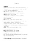
以下是典型的温度保护应用实例:1. 在电芯的正负极间串接PTC2. 电芯外电路主回路串接Breaker(断路器-可恢复)/Fuse.详细介绍一下保护芯片级联的具体工作情况。
还是以S-8204B为例,其CTLC端子可由芯片外部控制COP端子的输出电压、而CTLD端子则可由芯片外部控制DOP 端子的输出电压。
通过CTLC端子以及CTLD端子可以分别单独控制COP端子与DOP端子的输出电压。
并且,这些控制功能优先于芯片内部的电池充放电保护功能。
如果8节电池中的某一节电池发生过充,与该电池相连接的S-8204B的COP 端子输出电压会发生变化,该电压变化会传递到与其相连接的另一个S-8204B的CTLC端子,使得另一个S-8204B的COP端子输出电压也发生变化,从而控制充电控制用MOSFET关断,实现锂离子电池的过充电保护。
如果8节电池中的某一节电池发生过放电时,则由与该电池相连接的S-8204B的DOP端子向另一个S-8204B芯片的CTLD端子发出过放信号,改变其DOP端子的状态,最终使得放电控制用MOSFET关断,结束放电。
图2给出了采用两个S-8204B实现过充电保护的电路工作原理图(在N沟道MOSFET控制情况下),图3是过放电保护工作原理图。
图2锂离子电池过充电时的保护电路工作原理图图3锂离子电池过放电时的保护电路工作原理图充放电时的温度控制另外,对充放电过程的温度控制也是许多设计者需要考虑的。
高压包直接代换型号

原型号47105648 47105731 2385205300 2385205700 2385205900 2385206700 23852074002385210300 2385211900 154-195E 154-195Q 154-382A 154-382B 154-388F 154-388G 19.70009.001 19.70026.001 19.70032.001 19.70038.A01 19.70038.A11 19.70038.A21 19.70043.A01 19.70052.001 19.70052.011 19.70052.011 19.70056.S01 19.70060.001 35L515AZT 39L2024AZ 39L499AZT 490-170-6802 490-170-6802 6174T13011A 6174Z-1003D 6174Z-1003G6174Z-1008F 6174Z-1008J 6174Z-1012B6174Z-1012C 6174Z-1017H 6174Z-1024A 6174Z-1031A 6174Z-1031E6174Z-1036A 6174Z-1038A 6174Z-1038C 6174Z-1038D 6174Z-1038G6174Z-1045A 6174Z-1048A 6174Z-1054A 6174Z-1055A 6174Z-1057A 6174Z-1063A 6174Z-2001B 6174Z-2001C 6174Z-2001J 6174Z-2002A 6174Z-2002E 6174Z-2002F 6174Z-2002J 6174Z-2003C 6174Z-2003F 730-302-0564A 730-302-1433A 730-302-7681A 730-302-770VC 730-302-768FD 730-302-769FD 730-302-850M 730-302-X570A 759Z002-10 759Z003-1079A110-2-L79A355-179A355-379A355-4-A79A355-4-AS 79A-361-A79A761-2-B79A763B504 79A769-2-A79A769-2-C79A785F-1-AH 79A785F-2-AH 79A790-279A790-2-A79A790-2-AH9 79A9110-279A995-6-A79AS762-2 884-49602-34A 9602-44A99-40-60020001 AT20097/07A AT2009/33AT2090/36AT2090/38AT2090/39AT2094/02AT2094/03AT2094/23AT2094/24AT2097/01AT2097/05B AT2097/07A AT2097/14BAT2097/15AT2097/146 AT2097/18B AT2097/19AT2097/19AAT2097/21AT2097/33AT2097/34AT2097/36AT2097/38BH26-00017A BH26-00108A BH26-00109A BSC24-1402 BSC24-1402BSC24-1438BSC24-1445 BSC24-1448 BSC24-1454 BSC24-4005 BSC24-5375BSC24-5378BSC24-N2321S BSC24-N2330S BSC24-N2333S BSC24-N2360S BSC24-N2361S BSC24-N2374S BSC24-N2375S BSC25-0134 BSC25-0202A BSC25-0202C-1 BSC25-0208M BSC25-0218BSC25-0237MBSC25-024MBSC25-0251MBSC25-0252MBSC25-0405BSC25-0405ABSC25-1447BSC25-1448BSC25-1454BSC25-1459BSC25-1558SBSC25-6503B/37-SC2565-03BOX BSC25-M02H4 BSC25-M0A8N BSC25-N2310S BSC25-N2318SBSC25-Z2504BSC25-Z2505BSC26-0202BSC26-1450BSC26-1451BSC26-1453BSC26-1460BSC26-M02C1 BSM26-0202BSM26-0401BSM31-3305BSM31-3905BSM35-3219BSM35-3315BSM35-3316 /F770D BSM35-3316D /F772 BSM35-3316D/Q770 BSM54-320719.70038.A01BSM75-3707BSM75-3708BSM75-3709K/730-302--P6SEBSM75-3709M /730-302-796FDBSM75-3709N /730-302-796PFBSM75-3714BBTT550C7N44/ETF39L3005CZ CA-0215CF2154/LC-11/6174T11005ECFB-4/069CFB-4/120CTB-4/121C-FBT-1527C-FBT-1558SC-FBT-1770DFC-FBT-720AC-FBT-V770BC-FBT-V786ACJ28540ACJP28634-00ACT-8151CT-8204ACT-8255CT-8350CT-8355CT-8459CT-8459CT-8479CT-8662CT-8670CT-8821CT-9563C-THF-1466DG30000004021 DG96Q15848 DNF-FL2700DNF-FL2727DNF-FL2732A DNF-FL2732B ETF35L510AZT/313811878501 ETF35L7018AZ ETF35L7037AZ ETF39L2001AZ/313812874601 ETF39L2075AZB /313817876342 ETF39L3005AZ ETF39L3005BZ ETF39L3005CZ ETF39L3029AZ/2385210200ETF39L462AZT ETF39L639AZT/313811877581 ETF39L639AZT/313811877581 ETF39L86AZETF39L90AZETF40L2011AZ 3138 178 72201 FAO0019AFAO0135A /79A761-1-CFAO0200/79A763A FB-5B/CF1465FB-5B/CF1486 FBT-023FBT-025/FEA654 FCO-14A030C FCO-14A042FEA185AFEA237AFEA241FEA287BFEA287C /730-302-0564AFEA374FEA374FFEA382FEA383FEA469FEA469DFEA531AFEA531CFEA557FEA565AFEA602B /79A371-1C-TCFEA603A/79A371-1C-BFEA634/79A355-1FEA636FEA626/LZ250A.000PFEA662A/LZ250A.013PFEA677TBC000* 277FEA677/TBC000 * 277 FEA687FEA689/79A569-1FEA689/79A569-1DFEA689B/79A569-1-BFEA711A/79A769-1-AFEA711C/79A769-1-BFEA755FEA759DG3000008800 FEA780730-302-7681A FEA780B / 730-302-7601D FEA800A/79A955-1-A FEA800B/79A995-1-AH FEA817FEA824FEA825AFEA826FEA827FEA830FEA831FEA833FEA836FEA848AFEA850 / 2385208600 FEA850AFEA861/730-302-X975 FEA861 / 730-302-X975C FEA867A/ TFB-7012 FEA880FEA883FEA886/ 313816874001 FEA886A/313816878051 FEA888FEA888AFEA906FEA907FEA908/TFB-8503FEA915/79A769-1-C FEA937FEA937/79A371-1C-C FEA945B FEA946FEA946A FEA953/ TFB-7015 FEA976FEA978FEA73015H FFA76017U FFA76028U FFA76028U/F FFA79014U FFA81024U FFA81045 FFA81045H FFA81049H FFA82012H FFA82022H FFA82025H FFA86012D FJ2672FKD-14A001 FKD-15A001 FKD-15C003 FKD-15D002 FKG-15A001 FKG-15A006 FKG-15A007 FKG-15D001 FKH-17A001 FKH-17A002 FLO0108/ TFB-7021 FN/DNF1528 FN1434FPH0213 FQA-15A001FQB-17A001 FQB-17B015 FQM-15A007 FQM-15A007B FQM-15A009/B FQM-15B003 FQM-17A008 FQM-17A001 FQM-17A012 FQM-17B002FQM-17B007FQM-15B015 FQM-17B019 FQM-17B021 FSA0188FSA0210FSA0298FSA-15A002 FSA-15A003 FSD-15B002 FSD-15B002A FSN-14A024 FSN-14A029S FSN-15A008 FSN-15A008S FSN-15A019S FSN-15B027N FSN-15C004NFSW-17A001 FSW-17A002 FTX-14A015 FUA-17A010FUA-17A019 FUA-17C003 FUA-17C004 FUA-17C006 FWK0030 FWK0030A FWK0062BHFT264MKD-1731KD-1732PF-A KFS-60807A KFS-60854 KFS-61101 KFS-61140A KFS-61376 KFS-61410 KFS-61432 KFS-61478 KJF-9203D KJF-9215B KJF-9320C KJF-9458A KJF-9902B/F KJF-9902B/P LBCH011-000 LCE CF0394 LCE CF0590A LCE CF0590B LCE CF0612 /313811877590 LCE CF0612A /313811879410 LCE CF0612A /313811879410 LCE CF0625 /19.70026.001 LCE CF0689 /19.70028.001 LCE CF0698A LCE CF0706 LCE CF0710 LCE CF0724A LCE CF0754B LCE CF0801 LCE CF0821 LCE CF0857 LCE CF0857A LCE CF0883 LCE CF0910 LCE CF0929LCE CF0959 LCE CF0960 LCE CF0969 LCE CF0969A LCE CF0969B LCE CF0969C LCE CF1027 LCE CF1033A LCE CF1043 LCE CF1043E LCE CF1119A/313817875452 LCE CF1143 LCE CF1263/2850004510 LCE CF1280 LCE CF1285 LCE CF1380B / TFB-7010LCE CF1388B LCE CF1388C LCE CF1433 LCE CF1517 LCE CF1570 LCE CF1611 LCE CF1628 LCE CF1628 / 730-302-770VC LCE CF1648 LCE CF1737 LCE CF1741 LCE CF1781 LCE CF1821 LCE CF1827B LCE CF1873 LCE CF1920 LCE CF1921 LCE CF1938 LCE CF2091S LCE CF2101C/ 79A763ALZ250A 013J MF-2095MF-3131MF-3323MF-3323A MF-6114MF-6398MF-6407MF-6421MF-6540MF-6540B MF-6581/ 730-302-797N MF-6623 MSU1FVH002 TAD53712/LZ250A.013T TBC000*007 TBC000*033 TFB-016TFB023TFB025TFB-251T TFB-274T TFB-3501 TFB-3502 TFB-7002A/ FEA766A TRAN-6515 TRAN-8693V770Y265065CY265161Y265163Y265275Y265382Y265387Y265432BY265434 ZTFJ3385A ZTFJ73345A ZTFJ73369A/ 8000370直接代换型号47105647471057332385206700、39L2065AZ、FEA565A2385205900、CJ28540A、9502-20-100A、2385207400CJ28540A、2385205700、2385207400FEA565A、39L1057AZ、23852057002385205900、CJ28540A、39L2029AZ、2385205700LCE-CF1398、FEA850A、2385211800、9602-26A、2385211900、FEA850、2385208600、CJP28634-00A、2385208800、ETF39L3029AZ、2385210200 LCE、CF1938、FEA850A、2385211800、9602-26A、FEA850、2385208600、CJP28634-00A、2385208800、ETF39L3029AZ、2385210200、2385210300154-195Q154-195E6174Z-2001B、6174Z-2001CKFS-61410、KFS-61101、KFS-60807A、LCE、CF0710KJF-9458A、KJF-9320C、FEA2416174Z-2003C、FSN-15A008S、FSN-15A008、CFB-4/085A19.70038.A11、BSM54-3207、19.70026.00119.70038.A11、BSM54-3207、19.70009.001LCE、CF0754B19.70060.00119.70038.A01、19.70009.001、19.70026.00119.70038.A0119.70056.011、19.70052.011、19.70056.S01、FEA906、FEA907FEA906、FEA907、19.70056.S01、19.70056.01119.70043.A01、19.70056.011、19.70056.S01、FEA906、FEA90719.70052.001、FEA906、FEA907、19.70043.A01、19.70052.011、19.70056.S01 19.70052.001、FEA906、FEA907、19.70056.011、19.70043.A01、19.70052.011 19.70038.A01730-302-1433A.B、730-302-1433A、ETF39L462AZTLCE、CF0960、FEA47739L518AZT、FEA383、410-F013A、LCE CF1143、39L499AZT、410-F012B 79A769-2-A、MF-6540B、MF-6540、490-170-6540BSC25-Z25056174Z-1031E6174Z-2001J6174Z-1017H6174Z-1008J、FEA780、730-302-7681A、FUA-17A019、730-302-7681B、FUA-17A010、BSC25-14596174Z1008F、FEA780、730-302-7681A、FUA-17A019、730-302-7681B、FUA19A010、BSC25-14596174Z-1012C、6174Z-1031A6174Z-1012B、6174Z-1031A6174Z-1003G、39L1023AZY265434、Y2653826174Z-1012B、6174Z-1012C6174T13011A、JF0501-1754、BSM26-0401、6174T13005A、6174Z-1048A、6174Z1038DFEA826、79A355-4-A、FEA469、BSC25-6503/C-FBT-1527、79A355-1、FEA469D 、79A355-503、BSC24-1438、6174Z-1045A6174Z-1038D6174Z-1038G6174Z-1038A、6174Z-1048A、6174Z-1031E、BSM26-0401、6174T13005A6174Z-1038CBSC25-6503/C-FBT-1527、FEA469D、79A355-503、BSC24-1438、6174Z-1036A、79A355-5BSM26-0401、6174Z-1038D、6174Z-1031E、BSM26-0401、6174T13005A、6174T13011A6174Z-1055A、6174T11004A、6174Z-1057A、6174T11004C、6174Z-1063A6174T11005E、6174Z-1063A、6174T11004C、6174Z-1054A、6174Z-1057A、6174T11003E、LCE CF2154 / LC-116174T1055A、6174T11004A、6174Z-1054A、6174T11003E、6174Z-1063A、LCE CF2154/LC-11、6174T11004C6174Z-1055A、6174T11004A、6174Z-1057A、6174T11003E、6174Z-1054A、6174T11003E、LCE CF2154/LC-116174Z-2001C、154-382A6174Z-2001B、154-382A6174Z-1003D6174Z-2002FKFS-614326174Z-2002AKFS-61432730-302-0564A、FSN-15A008/、CFB-4/085A、154-388G、730-302-0564ABSM31-3305、730-302-850M、FSN-14A029S6174Z-2003C、730-302-0564A、FSN-15A008、FSN-15A008S 、CFB-4/085A、154-388G730-302-1433A(B)154-311B、ETF39L462AZT、730-302-1433、35L515AZT ETF35L7018AZ、630-302-1781、BSM75-3708LCE CF1628LCE CF1920、730-302-769FD、LCE CF1821LCE CF1920、730-302-786FD、LCE CF1821FSN-14A029S、730-302-850M、6174Z-2003F、FSN-14A003SFSN-15A019S、FSN-15B045N、6174Z-2003M759Z003-10759Z002-1079A99579A355-4-A、FEA826、FEA469、6174Z-1036A、79A355-5、BSC25-6503/C-FBT-152779A355-4-A、FEA634、79A355-1、79A355-4-AS、BSC25-6503/C-FBT-1527FEA634、79A355-1、79A355-3、CT-8492、79A355-4-AS、FEA826、FEA469、6174Z-1036A、79A355-5、BSC25-6503/C-FBT-1527、BSC24-N2330SFEA634、79A355-1、79A355-3、CT-8492、79A355-4-A、FEA826、FEA469、6174A-1036A、79A355-5、BSC25-6503/C-FBT-1527、BSC24-N2330SBSC25-M0A8N79A7902-2-A、79A761-1-A、FAO0019A、FAO0153A、79A761-1-C、79AS762-2、79A790-2、79A9110-2、79A790-2-AH9、FEA711A、FEA711C、FEA817ALCE CF2101C/79A736A、FAO0220 / 79A736A79A769-1-A FEA711A 79A769-2-C 79A769-1-C FEA915 490-170-6687FEA711A 79A769-1-A 79A769-2-A 79A769-1-C FEA915 79A995-6-AETF35L7019AZ79A785F-2-AH79A785F-1-AH79A9110-2 79A790-2-A 79A790-2-AH9 79A761-2-B79A761-2-B 79A761-1-A FAO0019A 79A790-2 79A9110-2 79A790-2-AH9 79A790-2-A 79A761-2-B 79A761-1-A FAO0019A 79A790-2 79A9110-279A790-2-A 79A761-2-B 79A761-1-A FAO0019A 79A790-2 79A790-2-AH9 79A769-6-C ETF39L3039AX79A761-2-BDG96Q1584819.70065.00119.70056.011CFB-4/069FEA636AT2094/01 ETF39L639AZT 313811877581 AT2090/36 AT2090/39 AT2094/03 AT2094/01 ETF39L639AZT 313811877581 AT2090/33 AT2090/39AT2094/03AT2094/01 ETF39L639AZT 313811877581 AT2090/33 AT2090/36AT2094/03 AT2090/39AT2094/01 AT2090/38 ETF39L639AZT 313811877581 AT2090/33AT2090/36 AT2094/03ETF39L639AZT 313811877851 LCE CF0612A 313811 79410 ETF35L510AZT 3138118778501 AT2094/03 AT2094/01ETF39L639AZT 313811877581 AT2090/33 AT2090/36 AT2090/39AT2094/02AT2094/24AT2094/23AT2097/15 AT2097/36ETF40L2011AZ 313817872201FEA636AT2097/18BAT2097/01 AT2097/36FEA557AT2097/14BETF39L2001AZ 31382874610FB-5B/CF1465 313816873091313816873121 313817876342 LCE CF1119A 313817875452 AT2097/38AT2097/33 AT2097/34 FSN-15C004NFSN-15C004N AT2097/21 AT2097/34 AT2097/38 313816873121 313817876342 LCE CF1119A 313817875452FSN-15C004N AT2097/21 AT2097/38 313816873121 313817876342 LCECF1119A 313817875452 AT2097/33AT2097/01、AT209715AT2097/21、AT2097/33、AT2097/34、FSN-15C004NFQA-15A001FEA831、FQB-17A001、LCE CF1648FQM-18B002、LCE CF1781、FSA0188BSC25-0202A、BSC26-M02C1、FEA237A、79A361-379A371-1T、FEA67878A355-502、FFA81049H、BSC25-6503/C-FBT-1527、79A566-1A、FEA469D、6174Z-1036A、79A355-5、6174Z-1045ABSC25-0202C-1、BSM35-3315BSC25-1447BSC25-1454TBC000*033、TBC000*00779A355-502、FFA81049H、BSC25-6503/C-FBT-1527、79A556-1A、FEA469D、6174Z-1036A、79A355-5、6174Z-1045A、79A355-4-ABSC26-145079A355-502、FFA81049H、BSC25-6503/C-FBT-1527、79A566-1A、FEA469D、6174Z-1036A、79A355-5、6174Z-1045A、79A355-4-A79A355-4-A、79A355-502、FEA81049H、BSC25-6503/C-FBT-1527、79A566-1A、FEA469D、6174Z-1036A、79A355-5、6174Z-1045AFEA771、DG300008800、TFB-7002A、FEA766A、BSC25-6503/C-FBT-1770DF BSC25-0208MBSM75-3709K、730-302-P6SELCE CF1827B BSM75-3709N 730-302-796PFBSM75-3709M 730-302-796FD BSC25-N2310S 730-302-786FD LCE CF1821 MF-3323A FFA79014U MF-3323BSC26-M02C1 FEA237A 79A361-3 BSC24-1402 79A361-1BSC24-1445 BSM35-3315LCE CF1517 BSC24N2360SFFA81045 FFA73015HBSC25-6503B/37-SC2565-03B0X BSC25-N2318S BSC25-0252M BSC25-6503/C-FBT-720A BSC25-0240M BSC25-Z2504/490-170-6707BSC25-6503B/37-SC2565-03B0X BSC25-N2318S BSC25-0252M BSC25-6503/C-FBT-720A BSC25-0237M BSC25-Z2504/490-170-6707TFB-016 MF-6114BSC25-6503B/37-SC2565-03B0X BSC25-N2318S BSC25-0240M BSC25-6503/C-FBT-720A BSC25-0237M BSC25-Z2504/490-170-6707BSC25-0405A BSC25-M02A4 BSC25-M02H4BSC25-M02A4 BSC25-M02H4 BSC25-0405BSC24-1448FQM17A008 6174T13010GBSC24-1454FUA-17A019/730-302-7681B FUA-17A010 BSC25-1459 6174Z-1008F/730-302-7681ABSC25-6503/C-FBT-1527BSC25-N2318S BSC25-0237M BSC25-0252M BSC25-0240M BSC25-6503/C-FBT-720A BSC25-Z2504/490-170-6707BSC25-0405A BSC25-M02A4 BSC25-040579A361-1BSC24-N2375S 730-302-786FD BSM75-3709M 730-302-796FDBSC25-6503B/37-SC2565-03B0X BSC25-0237M BSC25-0252M BSC25-0240M BSC25-6503/C-FBT-720A BSC25-Z2504BSC25-N2318S BSC25-0237M NSC25-0252M BSC25-0240M BSC25-6503/C-FBT-720A BSC25-6503B/37-SC2565-03B0X490-170-6802 CT-8662BSM37-3707 ETF39L3005CZBSC24-5378MF-6421 BSC26-1460 BSM26-0202 BSM75-3707 CT-8670 MF-6407BSC6503/C-FBT-V770B BSC25-6503/C-FBT-786ABSM75-3707 MF-6421 BSC26-1451BSC25-0202A FEA237A 79A361-3 BSC24-1402ETF35L7037AZ ETF35L7018AZ BSM75-3707 CT-8670 MF6407 BSC26-1451 ETF39L3005AZ ETF39L3005BZ ETF39L3005CZ6174Z-1048A 6174Z-1031E 6174Z1038D6174Z-2003F FSN-14A024 730-302-850D 730-302-850MFEA677 TBC000*277MF-3131 FFA81045H FFA73015HBSC25-0202C-1 BSC24-1445BSM35-3316D/Q770 V770 BSM35-3316D/F772 FQM-17B007BSM35-3316D/Q770 V770 BSM35-3316/F770D FQM-17B007V770 BSM35-3316D/F772 BSM35-3316/F770D FQM-17B00719.7003.001、LCE CF0698A LCE CF0625、19.70026.001 19.70038.A1119.70009.001 LCE CF0689 19.70028.001 19.70038.A21 19.70060.001BSC26-0202 BSC26-1460 BTT550C7N44 ETF39L3005CZ BSC26-1451CT-8670 MF-6470 BSC26-14517730-320-7681A ETF35L7018AZBSC24-N2361S 730-302-770VCBSC24-N2375S 730-302-786FD BSC25-N2310S 730-302-796FDBSC24-N2374S 730-302-796PF LCE CF1827B19.70043.A01 19.70052.011 19.70056.001 19.70056.S01 FEA906 FEA907BSM75-3707MSU1FVH0026174Z-1055A 6174Z-1063A 6174T11004C 6174Z-1054A 6174Z-1057A 6174T11003E99-40-60020001CT-8255FFA82025H FFA82022H LCE CF0801BSC24-N2321S BSC24-1438 79A355-4-A FEA826 FEA469 6174Z-1036A 79A355-5 79A355-1 BSC24-1438 79A355-503 BSC24-5375 6174Z-1045A BSC25-1558S 79A566-1A FEA469D(外7脚接7脚) BSC25-6503/C-THF-1466 79A355-4-ASBSC25-6503/C-THF-1466 BSC25-6503/C-FBT-1527BSC24-N2333S FEA771 DG300008800 TFB-7002A FEA766ABSC25-0252M BSC25-0240M BSC25-6503B/37-SC2565-03B0X BSC25-Z2504/490- 170-670 BSC25-0237MBSC25-6503/C-FBT-V786A BSC26-1453BSC25-6503/C-FBT-V770B BSC26-14532385205900 39L2029AZ 2385205700 23852074002385210300 2385208800LCE CF1873/730-302-566NBSC25-6503/C-FBT-1527 79A355-4-A FEA526 FWA469 6174Z-1036A79A355-5 79A355-1 BSC24-1438 79A355-503 BSC24-5375 6174Z-1045A BSC25-1558SCFB-4/120LFT0006-BFEA374 FEA374F 79A348-3FEA827 FEA825ACT-8221FBT-025 FEA654 6174Z2004EBSC25-Z2505/490-170-6802BSM26-0202 BSM75-3707 BSC26-1451CT-8459BSM31-3305 730-302-850M79A355-4-A 79A355-502 FFA81049H BSC25-6503/C-FBT-1527 79A566-1A FEA469D 6174Z-1036A 79A355-5 6174Z1045AFEA185A DG3000005311848-4FCO-14A030C KFS-61140AFCO-14A042 FTX-14A015DNF-FL2732BDNF-FL2732AWTF39L639AZT、313811877581 AT2094/02 LCE CF0612A、313811879410 730-302-7681A BSM75-3708 BSM26-0202 ETF35L7037AZBSM26-0202 ETF35L7018AZ 730-302-7681A BSM75-3708AT2097-19AT2097-21 FB-5B-CF1486 LCE CF1119A、313817875452BSM26-0202 ETF39L3005BZ ETF39L3005CZ BSM75-3707BSM26-2502 ETF39L3005AZ ETF39L3005CZ BSM75-3707BSM26-0202 ETF39L3005AZ ETF39L3005BZ BSM75-37072385210300 2385211900730-302-1433A.B 35L515AZTAT2090/33 AT2090/36 AT2090/39 AT2094/03AT2094/02 LCE CF0612A、313811879410 ETF35L510AZT、313811878501 ETF39L90AZETF39L86AZAT2097/05B79A761-2-B 79A790-2 79A9110-2 79A790-2-A 79A790-2-AH979A761-2-B FAO0153A、79A761-1-C 79A761-2-B 79A790-2-ALCE CF2101C、79A763A 79A763B504AT2097-19AAT2097-21 ETF39L2075AZB、313817876342 LCE CF1119A、313817875452 FBT-025、FEA654 CT-8479 6174Z-2004ECT-8479 6174Z-2004E FBT-023DNF-FL2700 KFS-61140AFTX-14A015 DNF-FL2727DG300004021BSC25-0202A BSC26-M02C1 BSC24-1402、79A361-1KJF-9458A KJF-9320C 730-302-1433BFEA86012D LCE CF0724A ZTFJ73345AFEA287C、730-302-0564AFEA287BCT-8355、79A348-3 FEA374F 79A348-1AFEA374 CT-8355、79A348-3 79A348-1ALCE CF091039L518AZT LCE CF1143 39L499AZTFEA826 75A355-4-A 6174Z-1036A 79A355-5 79A355-1 BSC25-6503/C-FBT-1527 6174Z-1045A BSC24-1438BSC25-6503/C-FBT-1527 79A355-503 BSC24-1438 6174Z-1036A 79A355-5 6174Z-1045A、79A355-1FEA531CFEA531AAT2097/1639L2065AZ、2385206700 39L1057AZ、2385205300FEA603A、79A371-1C-BFEA602B、79A371-1C-TCFEA826 79A355-4-A(S) 6174Z-1036A 79A355-5 79A355-1 BSC25-6503/C-FBT-1527 6174Z-1045A BSC24-1438AT2097/07AFEA662A、LZ250A.013P LZ250A013J TAD53712、LZ250A.013TFEA662、LZ250A.000P LZ250A 013J TAD53712、LZ250A.013TBSM31-3905、TBC000 *150ABSM31-3905、TBC000 * 150ABSC24-1420 730-312-1434BSC25-6503/CFBT-1527 CT-8204A 6174Z-1045A BSC24-1438 79A355-4-A(S) 6174Z-1036AFEA689B、79A569-1-B FEA937、79A371-1C-CFEA689、79A569-1D79A769-2-A 79A769-2-C 79A769-1-C 79A761-2-B FEA817A 79A769T-1-B FEA945B FEA915 FEA711C、79A769-1-B79A769T-1-B FEA945B 79A761-2-B FEA817A FEA915、79A769-1-CFEA711A、79A769-1-A 79A769-2-AFKG-15A001 FN1434FKH-17A002 FKH-17A001BSC24-N2333S FEA766A BSC25-6503/C-FBT-1770DFFEA880 6174Z-1008F、730-302-7681A MF-6398 FEA780BFEA780、730-302-7681A FEA880 61714Z-1008F、730-302-7681A MF-6398 FEA780BFEA800B/79A995-1-AHFEA800A、79A955-1-A79A769-1-B、FEA711C 79A769T-1-B、FEA945B FEA711A 79A761-2-BFKD-15D002FEA827 CT-8459、LFT000779A355-4-A FEA469 6174Z-1036A、79A355-5 79A355-1 BSC25-6503/C-FBT-1527 6174Z-1045A 79A355-4-AHCT-8459、LFT0007 FEA825AFKG-15A001 FKG15A006FQB-17A001 LCE CF1648、BH26-00108A FSA0188LCE CF1741/730-302-572CFEA861A/730-302-X975C FEA861/730-302-X975FSN-15B052N/730-302-566DA2385210300 LCE CF1938 FEA850A 2385211800 23852119002385210300 LCE CF1938 FEA850 2385211800 2385211900FEA836、730-306-X759 FEA861 、730-302-X975CFEA836、730-302-X975 FEA861、730-302-X975FEA908、TFB-8503 FEA883 LCE CF1380B、TFB-7010 FEA976 FEA978FEA780FEA867A、TFB-7012 FEA908、TFB-8503 LCE CF1380B、TFB-7010 FEA976 FEA978FSN-15C004N FEA888 FEA88A、313816878061FEA888A、313816878061FEA886、313816874001 FSN-15C004N FEA888 FEA888AFEA886、313816874001 FSN-15C004N FEA888 FEA886A、313816878051 FEA907 19.70052.001 19.70056.S01 19.70056.00179.70052.001 FEA906 19.70056.S01 19.70056.011FEA867A、TFB-7012 FEA883 LCE CF1380B、TFB-7010 FEA976 FEA97879A769-2-A 79A769-1-A FEA711A 79A769-2-CFEA711A、79A769-1-A、9602-04-101A FEA711C、79A769-1-BHFT264MFEA689、79A569-1D79A769-1-B FEA711C FEA711A FEA817AFWK0062B、730-302-797N MF-6581、730-302-797N FEA946A LCE CF1737 FEA946 FWK0062B、730-302-797N MF-6581、730-302-797N LCE CF1737 FLO0108、TFB-7021FEA867A、TFB-7012 FEA883A FEA908 FEA978 LCE CF1380B、TFB-7010 FEA867A、TFB-7012 FEA883A FEA908 FEA976 LCE CF1380B、TFB-7010 MF-3131、5RH0000108 BSM35-3219 FFA81045H BSC25-0218FFA76028U FFA76028U/FFFA76017U FFA76028U/FFFA76028U FFA76017UMF-3323A MF-3323 BSC25-0134LCE CF0883BSC25-0218 FFA81045H FFA73015H BSM35-3219MF-3131、5RH0000108 BSM35-3219 FFA73015H79A355-503 BSC24-1438 BSC25-6503/C-FBT-1527 79A355-4-AFFA82022HFFA82025H CFB-4/121、M374392 LCE CF0801 FFA82012HFFA82022H CFB-4/121、M374392 LCE CF0801FEA284、5RH0000060 LCE CF0724A ZTFJ73345AKJF-9215BFKD-15A001 FKD-15C003 FN/DNF1528FKD-14A001 FKD-15C003 FN/DNF1528FKD-14A001 FKD-15A001 FN/DNF1528FEA824FEA755 FN1434 FKG-15A006(3、4脚对换)FEA830 FKG-15A001(3、4脚对换)FQM-15A009FKG-15D002(将聚焦盒引脚向下右两脚连接)FKH-17A002 FEA759FEA759 FKH-17A001FEA953、TFB-7015FKD-14A001 FKD-15A001 FKD-15C003FEA755 FKG-15A001LCE CFT2091SBH26-00017AFEA831 LCE CF1648、BH26-00108A FSA0298FSA0188 FQB-17B002FQM-15A007B FQM-15A009/BFQM-15A007 FQM-15A009/BFQM-15A007B FQM-15A007FSA0210BSC25-1448、6174T11006BFQM-17A012FQM-17A011BH26-00109A LCE CF1781 FQM-17B015 FSA0188BSM35-3316DQ770 V770 BSM35-3316D/F772 BSM35-3316/F770D LCE CF1570、2850007210FQM-15B002FQM-17B021FQM-17B019BH26-00109A LCE CF1781 FQM-17B015 FQM-17B002FQM-15B003FQB-17A001 FEA831 LCE CF1648、BH26-00108AFSA-15A003FSA-15A002FSD-15B002AFSD-15B002BSM31-3305、730-302-850M 6174Z-2003H6174Z-2003F 6174Z-2003H6174Z-2003C FSN-15A008S 154-388G CFB-4/085A6174Z-2003C FSN-15A008 CFB-4/085A 154-388G730-302-X570A FEA708ATFB-274T FEA848A、730-302-566DBFEA886、313816874001 FEA888 FEA888A、3138 168 78061 AT2097-33 AT2097-34 AT2097-21 AT2097-38FSW-17A002FSW-17A001FCO-14A042 DNF-FL2727TRAN-8693、530-302-700SA BSC25-1459 MF-6623 FUA-17A019 6174Z-1008F MF-6398FUA-17A010 TRAN-8693、530-302-700SA BSC25-1459 MF-6623 6174Z-1008F MF-6398FUA-17C004 FUA-17C006FUA-17C003 FUA-17C006FUA-17C003 FUA-17C004LCE CF1628、730-302-770VC FWK0030AFWK0030 LCE CF1628、730-302-770VCFEA946 MF-6581、730-302-797N LCE CF161179A371-1C-C FEA937KD-1732PF-A(5,7脚空)FSA0298KD-1731 FSA0298KFS-61410 KFS-61101 154-382B LCE CF0710LCE CF0394KFS-61410 154-382B LCE CF0710 KFS-60807AFCO-14A030C DNF-FL2700LCE CF1280KFS-61101 154-382B LCE CF0710 KFS-60807A6174Z-2002E 6174Z-2002JLCE CF0929LBCH0110-000FJ2672KJF-9458A 154-388F、730-302-1433B FEA241、730-302-1433KJF-9320C 154-388F、730-302-1433B FEA241、730-302-1433KJF-9902B/PKJF-9902B/FKJF-9203DKFS-60854LCE CF0590BLCE CF0590ALCE CF0612A、313811879410ETF39L639AZT、313811877581 ETF35L510AZT、313811878501 AT2094-02 LCE CF0612/313811877590BSM54-3207、19.70038.A01 LCE CF0698A、19.70034.001 LCE CF0689、19.70028.001BSM54-3207、19.70038.A01 LCE CF0698A、19.70034.001 LCE CF0625、19.70026.001LCE CF0625 BSM54-3207、19.70038.A01 LCE CF0698Y265161 Y265163KFS-61410 KFS-61101 154-382B KFS-60807AFEA284、5RH0000060 FFA86012D ZTFJ73345A19.70032.001FFA82025H FFA82022H CFB-4/121/M374392TFB-251T、5062625120LCE CF0857A、313812875530LCE CF0857FFA81024UFEA382、HH00002KFS-61478HH00000139L2024AZ、HH000005 FEA477、HH00005LCE CF0969B LCE CF0969C LCE CF1033A LCE CF0969ALCE CF1033A LCE CF0969B LCE CF0969C LCE CF0969LCE CF0969 LCE CF0969C LCE CF0969A LCE CF1033ALCE CF0969 LCE CF0969B LCE CF0969A LCE CF1033ALCE CF1263、2850004510LCE CF0969 LCE CF0969B LCE CF0969A LCE CF0969CLCE CF1043ELCE CF1043、0480-0000-0040AT2097-21 FB-5B/CF1486、313816873121 AT2097-33 AT2097-34ETF39L2075AZB、313817876342 AT2097-3839L518AZT FEA383 39L499AZT、410-F012BLCE CF1027KFS-61376LCE CF1433、47F13-0911A LCE CF1611、47F13-1090BFEA867A、TFB-7012 FEA908、TFB-8503 FEA883LCE CF1388CLCE CF1388BLCE CF1611 LCE CF1285BSC25-0208M TRAN-6516 BSC25-0208MFQM-17B007LCE CF1433、47F13-0911A LCE CF1285、47F13-0910A730-302-770VCFWK0030 FWK0030AFEA831 FQB-17A001 BH26-00108AFEA946A、47F13-1091S MF-6581、730-302-797NFEA833、730-302-566DHBH26-00109A FQM-17B002 FSA0188BSC24-N2375S、730-302-786FD LCE CF1920 730-302-796FDBSC24-N2374S、730-302-796PF BSM75-3709N、730-302-796PF LCE CF1921 CT-8151、331100000107LCE CF1821 730-302-786FD 730-302-796FDLCE CF1827B BSC24-N2374S BSM75-3709N2385210300 FEA850 FEA850A 2385211900FPH021379A763B504 FAO0220/79A763AFEA662、LZ250A.000P FEA662A、LZ250A.013P LZ250A.013TY265065CBSM35-3219 FFA81045H FFA73015HMF-3323A FFA79014U BSC25-0134FFA79014U BSC25-0134 MF-3323BSC25-0251M、37-SC25M0-2510X TFB-016、5062601600FEA780、730-302-7681A FUA-17A010 FEA880BSM26-0202 BSM75-3707 CT-8670、KTC9970 BSC26-1451BSC26-1451 BSC26-1460490-170-6540 MF-6540B 490-170-6687490-170-6687 490-1706540 MF-6540FWK0062B、730-302-797N FEA946 FEA946A LCE CF1737FUA17010 TRAN-8693 、530-302-700SACA-0215FEA662、LZ250A.000P FEA662A、L250A.013P LZ250A 013JTBC000*033 BSC24-4005BSC24-4005 TBC000*007BSC25-0251M、37-SC25M0-2510X MF-6114TFB025TFB023LCE CF0821FSN-15B027NTFB-3502TFB-3501BSC24-N233S FEA771 BSC25-6503/C-FBT-1770DFLCE CF1517FUA17010 MF-6623BSM35-3316D/Q770 BSM35-3316D/F772 BSM35-3316/F770D FQM-17B007 MF-2095LCE CF0706 Y265163Y265161 LCE CF0706Y265387 Y265432BY265434 6174Z-1024AY265275 Y265432BY265387 Y2652756174Z-1024A Y265382ZTFJ73369A、80000371FEA284、5RH0000060 FFA86012D LCE CF0724AZTFJ3385A。
2009年到2012年电池市场发展透析(内容涉及锂电池、铅酸、及镍氢电池)
第一章锂电池相关概述1.1 锂电池的定义及分类1.1.1 锂电池的定义锂电池是一类由锂金属或锂合金为负极材料、使用非水电解质溶液的电池。
最早出现的锂电池来自于伟大的发明家爱迪生,使用以下反应:Li+MnO2=LiMnO2该反应为氧化还原反应,放电。
由于锂金属的化学特性非常活泼,使得锂金属的加工、保存、使用,对环境要求非常高。
所以,锂电池长期没有得到应用。
但现在锂电池已经成为了主流。
1.1.2 锂电池的分类锂电池分成两大类:不可充电的和可充电的两类。
不可充电的电池称为一次性电池,它只能将化学能一次性地转化为电能,不能将电能还原回化学能。
如锂二氧化锰一次电池、锂-亚硫酰氯一次电池。
而可充电的电池称为二次性电池(也称为蓄电池)。
它能将电能转变成化学能储存起来,在使用时,再将化学能转换成电能,它是可逆的,如市面上常见的锂离子手机电池。
1.锂电池外型分:有方型锂电(如常用的手机电池电芯)和柱形(如18650);2.锂电池外包材料分:铝壳锂电池,钢壳锂电池,软包电池;3.锂电池从正负极材料(添加剂)分:沽酸锂(LiCoO2)电池或锰酸锂(LiMn2O4),磷酸铁锂电池,一次性二氧化锰锂电池;另一分:锂离子LIB,聚合物PLB4.不同的性能用途方面分:一次性---锂锰电池--扣式3伏电池高容量(高平台)--用在手机数码产品上高倍率;---用在电动车和电动工具上及飞机模型高温;---矿灯,室上灯饰,机器内置后备电源;低温;---室外环境,北方(冬天)南极;- - 111.1.3 锂电池的主要特点1、具有更高的重量能量比、体积能量比;2、电压高,单节锂电池电压为3.6V,等于3只镍镉或镍氢充电电池的串联电压;3、自放电小可长时间存放,这是该电池最突出的优越性;4、无记忆效应。
锂__________电池不存在镍镉电池的所谓记忆效应,所以锂电池充电前无需放电;5、寿命长。
正常工作条件下,锂电池充/放电循环次数远大于500次;6、可以快速充电。
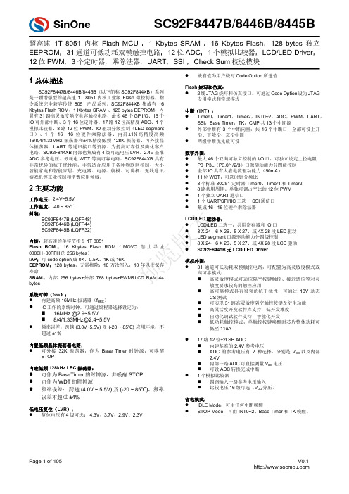
TDA8204B资料
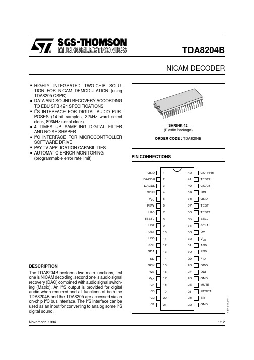
TDA8204BNICAM DECODERNovember 1994PIN CONNECTIONS.HIGHLY INTEGRATED TWO-CHIP SOLU-TION FOR NICAM DEMODULATION (using TDA8205 QSPK).DATA AND SOUND RECOVERY ACCORDING TO EBU SPB 424 SPECIFICATIONS.I 2S INTERFACE FOR DIGITAL AUDIO PUR-POSES (14-bit samples, 32kHz word select clock, 896kHz serial clock).4 TIMES UP SAMPLING DIGITAL FILTER AND NOISE SHAPER.I 2C INTERFACE FOR MICROCONTROLLER SOFTWARE DRIVE.PAY TV APPLICATION CAPABILITIES .AUTOMATIC ERROR MONITORING (programmable error rate limit)DESCRIPTIONThe TDA8204B performs two main functions, first one is NICAM decoding, second one is audio signal recovery (DAC) combined with audio signal switch-ing (Matrix). An I 2S output is provided for digital audio when required and all functions of both the TDA8204B and the TDA8205 are accessed via an on-chip I 2C bus interface. The I 2S interface can be used as an input for converting to analog some I 2S digital sound.1/12PIN ASSIGMENT8204B -01.T B LBLOCK DIAGRAMABSOLUTE MAXIMUM RATINGSTHERMAL DATATDA8204B2/12ELECTRICAL CHARACTERISTICS (T amb = 25o C, V DD = 5V, unless otherwise specified)SUPPLYOUTPUTSINPUTSBI-DIRECTIONALI C INTERFACETDA8204B3/12ELECTRICAL CHARACTERISTICS (continued)I C BUS TIMINGFigure 1 : I 2C Serial Bus TimingFigure 2 : I 2S Bus Timing DiagramTDA8204B4/12Figure 3 : NICAM Decoder Block DiagramFUNCTION DESCRIPTIONThe TDA8204B is partitioned into 6 major parts shown in the block diagram.The NICAM Decoder performs data and sound recovery from the signals specified in EBU SPB 424. The expanded digital audio signals (14-bit) are made available at the digital audio interface (I 2S) in a serial multiplex of left and right channels. They are also processed by a 4 times upsampling digital filter and noise shaper which results in a high speed digital data stream at the output pins DACDL/DACDR. This data stream can be applied to the 1-bit D-A convertors contained in the TDA8205.The TDA8204B is I 2C bus controlled and provides control over the functions of the TDA8205 by means of a serial inter-chip bus.1 - NICAM Decoder1.1 - BLOCK DIAGRAM (see Figure 3)1.2 - DESCRIPTIONNICAM frame alignment requires searching out a frame alignment word (FAW) and a 16 frame se-quence conveyed by C0 bit. Because of noise,interferences, errors in the incoming NICAM Data,aliases of the FAW, a robust scheme is imple-mented. It ensures the decoder will align, and stay aligned, to signals beyond the limit of maximum useable error rate. Thanks to a 511 bit PRBS syn-chronized by the recovered clock and a modulo 2adder, original data are recovered. This data stream can be processed externaly for de-encryp-tion in Pay TV applications using descrambled data Pins DDO, DDI.To allow simultaneous reading and writing of mono/stereo samples, de-interleaved data frames are stored in a 3 page RAM.The 10-bit input audio samples are expanded to 14-bit using scale factor bits according to NICAM decoding rules. Samples in error by the parity check are replaced by interpolated one or re-peated.Mute is set according to an error counter when the error rate exceeds error rate limit (ERL) and reset when the error rate is below ERL/4.Application control information (bit C1, C2, C3, C4)is recovered by majority decision logic over 16frames. the C1, C2, C3 , C4 bits can be read in SR0register and are set on the C1, C2, C3, C4 pins according to the state of bit 0 (BEA) of the CR2register.2 - Digital Filter and Noise ShaperA digital filter performs 4X upsampling in two stages. The main FIR 2x upsampler is followed by a smaller 2x FIR upsampler. Digital upsampling means a much simpler post-DAC reconstruction filter can be used thus saving on external compo-nent count and cost.A noise shaper converts the samples from the digital filter into two high speed serial bitstreams which can be applied to the DACs in the TDA8205.3 - I 2S BusA standard three-wire interface, conforming to the I 2S bus protocol, is provided, allowing connection of an external DAC or DAT interface. Audio samples contain 14-bit, so 16-bit DACs will pad the two LSBs with 0. The word select clock operates at 32kHz and the serial clock at 896kHz.By setting SDI bit of CR2 to 1, the I 2S interface can receive the digital I 2S sound. This prevents dupli-cating the dual D/A converter.TDA8204B5/124 - Interchip BusA one-line serial bus provides interchip communi-cations allowing control of all functions through the single I 2C bus interface.5 - I 2C BusAn I 2C bus interface provides access to control and status registers within the two chips to allow control of their functions and monitoring of status. A digital filter is included to improve noise immunity.5.1 - DATA FLAGS (see Figure 4)These indicate the status of the descrambled data on the DDO pin. They are inhibited if the decoder is out of alignement.-FID : Frame alignment word (scrambled)-PDV : Parity Data Valid. CIB0 and CIB1 overwrite the first 2 bits of FAW-ADV : 11 additional data bits-DV : Data valid (mode dependant)5.2 - DECRYPTION (see Figure 5)The PRBS generator (used for descrambling) is normally preset to all ones at the start of each frame. However, it is possible to preset it to any value on each frame by means of a code word clock (CWC) and serial code word data (CWD) interface on pins SEL0 and SEL1.CWD, which is clocked in on the negative going edges of the CWC clock, can be sent anywhere during the frame except when FID = 1. The CWC is asynchronous with respect to the Nicam clock and the CWD will be used on the following frame.During the time FID = 1, the levels on the SEL0,SEL1 pins are read for language selection. Code words for descrambler presetting may be sent in either an 8-bit or 9-bit formats. There are four possibilities :-if 7 or less clock cycles are counted on CW-clock during a frame, the PRBS generator is preset to all ones ;-if 8 clock cycles are counted, 8 bits of CW-data are clocked into the shift register, the first bit of the previous transfer now moving to bit 9 position in the shift register. The resulting value is used to preset the PRBS generator on the next frame.-if 9 clock cycles are counted, the CW-data (which has been clocked into a 9-bit shift register) is used to preset the PRBS generator on the next frame.-if 10 or more clock cycles are counted, only the first 9 bits of the CW-data are used and loaded into the PRBS generator on the next frame.Figure 4 :Data FlagsFigure 5 : PRBS PresetterTDA8204B6/125.3 - SOFTWARE SPECIFICATIONSoftware control of IC’s is given by programming four registers, one read only status register (SR0)and three read and write control registers (CR1,CR2, CR3).Transmit format :S = Start, A = AcknowledgeP = stopReceive format :Note :All registers are read sequentially; device status and thecontents of all registers may be read. The sequence may be terminated by not acknowledging (NOACK) the slave.Chip addressHAO : Hardware address selection pinRegister addressesRegister contentsSR0 : NICAM status (read only)L/S :•If FN1 bit of CR2 is 0, LS bit is loss of frame alignment status LS =1, FAW is lostLS = 0 FAW is identified•If FN1 bit of CR2 is 1, LS bit is selected system statusLS = 1, B/G standard LS = 0, I standardLA2:Loss of sub-frame alignment (1 = loss of alignment)MUT :NICAM mute (1 = DAC outputs muted)C4:Reserve sound flag (1 = FM backup)C3:Application control bit 3C2:Application control bit 2C1:Application control bit 1US2:User bit 2 (input)US2 bit indicates the state of US2 input PinCR1 : Matrix and mutes (read and write register)Qn :Output select (see tables)In :Input select (see tables)G0:Auxiliary output gain, 0 = 0dB, 1 = 6dB AUM:Auxiliary output mute, 0 = no-mute,1 = mutedFRE :Free run clock VCXO for set up,0 = normal, 1 = free runTo set crystal series capacitorSwitches and Matrix DescriptionFigure 6Output selectionMute and gain selection* Mute is activated by left channel selection ** Gain is activated by right channel selectionInput selectionExample of programming First step :0 0 1 0 0 X X X INTL connected to AOL, mute ON onAOL/AORSec-ond step :0 1 0 1 1 X X XEAIR connected to AOR, gain 0dB on AOL/AORThrird step :0 0 0 0 0 X X X INTL connected to AOL, mute OFF onAOL/AORThe power up default configuration is 0dB and unmute for both channels AOL/R, and INTL con-nected to AOL, and INTR connected to AOR.TDA8204B7/12CR2 : NICAM control (read and write register)SDI :I 2S direction0 = Output, 1 = InputECT :Bit error rate counting time 0 = 128ms, 1 = 64ms MAE :Max allowed errors 0 = 511, 1 = 255FN1:Set function of bit 0 in SR0, 0 = loss of alignment (status), 1 = system status (I or B/G)UMT :Un-mute NICAM, 1 = un-mute, 0 = mute LA1:Language select 1 (LA1 ⊕ SEL1)LA0:Language select 0 (LA0 ⊕ SEL0)BEA:Set C1-C3 functionUn-mute at BER/4.Note :C4 pin remains unchanged. The function of C1-C4 in SR0remains unchanged.CR3 : Switches (read and write register)US1:User bit 1 (output)US0:User bit 0 (output)AUT :Automatic selection, 1 = enable IBG :Select system I or B/G, 1 = B/G FSn :Force switch (see table)SYN :1 = synthesiser, 0 = dual VCXO(carrier loop)NICAM STAND-ALONE APPLICATIONThe NICAM kit has been designed to be monitored by the I 2C bus; nevertheless stand-alone working capability is offered to the designer for low costapplications.In order to know the status of the kit in stand-alone mode, consider the contents of the four I 2C regis-ters at power-ON (4 registers : SR0 - CR1 - CR2 -CR3). Hardware configurable pins will be described later.1 - Power-ON ConfigurationSR0 (status)US2:Not used in stand-alone C1:Application control bit status for NICAM signalC2:C3:C4:Reserve Sound FlagMUT :DAC outputs muted (demuted as soon as NICAM appears)LA2:the subframe alignment is been lost L/S:FAW status (FN1 of CR2 = 0)CR1 (R/W)Q1:NICAM sound is sent on all matrix outputs and on AMOx pins Q0:I2:I1:G0:Gain = 0dB on AMOx AUM :AMOx pins un-muted FRE:VCXO in normal modeCR2 (R/W)SDA :Normal mode ECT &MAE :BER = 1/112FN1:Bit L/S of SR0 set to alignment loss statusUMT :TDA8204B mute pin 25 to 0LA1:Result depending of SEL1LA0:Result depending of SEL0BEA :Beacon decoding mode but all diodesare OFF until a NICAM signal has been foundCR3 (R/W)US1:Not used in stand-by mode US0:Not used in stand-by mode AUT :Automatic standardTDA8204B8/12Figure 7IBG :Standard I (don’t care)FSn :Set to Auto NICAM (if NICAM fails, FM mono is selected)FN2:Not usedSYN:Synthesizer selected2 - Hardware Configurable Pins 2.1 - TDA8204B - PIN 6 - (RSW)-as an output :status of the RSW switch -0 = FM mono -1 = NICAM-as an input :-0 = FM mono (forced)2.2 - TDA8204B - PINS 34/35 - (SEL0/SEL1)(see Figure 7)-to select the language in case of bilingual opera-tion-selected value is related to LA0 and LA1As the I 2C bus is not used LA0 and LA1 = 0(power-ON condition) / SEL0 = Q0, SEL1 = Q1The 4 choices are summarized in the table below.M1 = Mono 1M2 = Mono 2VII - 2.3. TDA8204B - PIN 25 - (MUTE)-as an output :status of the DAC -0 = unmuted -1 = muted-as an input :-0 = unmute DAC (forced)TDA8204B9/12APPLICATION DIAGRAMSFigure 8 : Stand Alone Application (I standard)TDA8204B10/12Figure 9 : I 2C Bus Controlled Application (I and B/G standard)TDA8204B11/12PACKAGE MECHANICAL DATA42 PINS - PLASTIC SHRINKInformation furnished is believed to be accurate and reliable. However, SGS-THOMSON Microelectronics assumes no responsibil-ity for the consequences of use of such information nor for any infringement of patents or other rights of third parties which may result from its use. No licence is granted by implication or otherwise under any patent or patent rights of SGS-THOMSON Micro-electronics. Specifications mentioned in this publication are subject to change without notice. This publication supersedes and replaces all information previously supplied. SGS-THOMSON Microelectronics products are not authorized for use as critical com-ponents in life support devices or systems without express written approval of SGS-THOMSON Microelectronics.© 1994 SGS-THOMSON Microelectronics - All Rights ReservedPurchase of I 2C Components of SGS-THOMSON Microelectronics, conveys a license under the Philips I 2C Patent. Rights to use these components in a I 2C system, is granted provided that the system conforms tothe I 2C Standard Specifications as defined by Philips.SGS-THOMSON Microelectronics GROUP OF COMPANIESAustralia - Brazil - China - France - Germany - Hong Kong - Italy - Japan - Korea - Malaysia - Malta - Morocco The Netherlands - Singapore - Spain - Sweden - Switzerland - Taiwan - Thailand - United Kingdom - U.S.A.TDA8204B12/12。
S和DWA主流锂电池保护板原理图说明
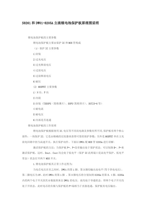
S8261和DW01-8205A主流锂电池保护板原理图说明锂电池保护板的主要参数锂电池保护板主要由保护IC和MOS管构成(1)保护IC主要参数1)封装2)过充电压3)过充释放电压4)过放电压5)过放释放电压6)耐压(2) MOSFET主要参数1) N沟、P沟2)内阻3)封装(TSSOP8 <简称薄片>、SOP8<简称厚片>、SOT23-6等)4)耐电流5)耐电压6)内部是否连通锂电池保护板的工作原理锂电池保护板根据使用IC,电压等不同而电路及参数有所不同,保护板有两个核心部件:一块保护IC,它是由精确的比较器来获得可靠的保护参数;另外是MOSFET串在主充放电回路中担当高速开关,执行保护动作。
下面以DW01配MOS管8205A进行讲解:激活保护板的方法:当保护板P+、P-没有输出处于保护状态,可以短路B-、P-来激活保护板,这时,Dout、Cout均会处于低电平(保护IC此两端口是高电平保护,低电平常态)状态打开两个MOS开关。
1.锂电池保护板其正常工作过程为:当电芯电压在至之间时,DW01的第1脚、第3脚均输出高电平(等于供电电压),第二脚电压为0V。
此时DW01的第1脚、第3脚电压将分别加到8205A的第5、4脚,8205A 内的两个电子开关因其G极接到来自DW01的电压,故均处于导通状态,即两个电子开关均处于开状态。
此时电芯的负极与保护板的P-端相当于直接连通,保护板有电压输出。
2.保护板过放电保护控制原理:当电芯通过外接的负载进行放电时,电芯的电压将慢慢降低,同时DW01内部将通过R1电阻实时监测电芯电压,当电芯电压下降到约时DW01将认为电芯电压已处于过放电电压状态,便立即断开第1脚的输出电压,使第1脚电压变为0V,8205A内的开关管因第5脚无电压而关闭。
此时电芯的B-与保护板的P-之间处于断开状态。
即电芯的放电回路被切断,电芯将停止放电。
保护板处于过放电状态并一直保持。
开关电源IC芯片

开关电源IC芯片Fairchild仙童(飞兆)系列开关电源驱动芯片FAN100MY、FAN102MY、FAN103MY、FAN6208、FAN6300AMY、FAN6754AMRMY、FAN6862TY、FAN6921MRMY、FAN6961SZ、FAN7346MX、FAN7384MX、FAN7319MX、FAN7527BMX、FAN7527BN、FAN7554N、FAN7554D FAN7621、FAN7621SSJ、FAN7621B、FAN7631、FAN7930CMX;FAN6204MY FL103、FL6300A即FAN6300、FL6961、FL7701、FL7730、FL7732、FL7930B、FL7930C、FLS0116、FLS3217、FLS3247、FLS1600XS、FLS1700XS、FLS1800XS、FLS2100XSFSFR1600、FSFR1600XSL、FSFR1700、FSFR1700XS、FSFR1700XSL、FSFR1800、FSFR1800XS、FSFR1800XSL、FSFR2100XSL、FSFR2100FSCQ0565RTYDTU、FSCQ0765RTYDTU、FSCQ1265RTYDTU、FSCQ1565RTYDTU FSDL321、FSDH321、FSDL0165RN、FSDM0265RNB、FSDH0265RN、FSDM0365RNB、FSDL0365RN、FSDM0465REWDTU、FSDM0565REWDTU、FSDM07652REWDTU、FSDM311、FSDM311A、FSEZ1016AMY、FSEZ1317NY、FSEZ1317MYFSGM0465RWDTU、FSGM0565RWDTU、FSGM0765RWDTUFSL106HR、FSL106MR、FSL116LR、FSL206MRN、FSL126MR、FSL136MR、FSQ100、FSQ110、FSQ321、FSQ510、FSQ0165RN、FSQ0170RNA、FSQ0265RN、FSQ0270RNA、FSQ0365RN、FSQ0370RNA、FSQ0565RSWDTUSG6105ADZ、SG6859ATZ、SG5842KA5L0380RYDTU、KA5M0365RYDTU、KA5M0365RTU、KA5M0380RYDTU、KA3525A、KA3842AC、KA3842AE、KA3842B、KA3843B、KA3844B、KA7500Con-bright昂宝系列电源驱动芯片超低待机功耗产品系列:OB5269、OB5269B、OB2273、OB2273A、OB2273B、OB2273F、OB2273N、OB2276、OB2276A原边控制系列产品:OB2520、OB2520D、OB2520M、OB2532、OB2531;OB2535/OB2535E、OB2536/OB2536E、OB2538/OB2538E、OB2539、OB2211、OB2211H、OB2212、OB2216准谐振模式控制芯片系列:OB2201/T、OB2202、OB2203PWM控制芯片系列产品:OB5269、OB5269B、OB2273、OB2273A、OB2273B、OB2273F、OB2273N、OB2361、OB2361P、OB2262、OB2263、OB2268、OB2269、OB2278、OB2279、OB2287、OB2288、OB2298、OB5222、OB5225、OB2353/L、OB2354/L、OB2356/L、OB2357/L、OB2358/L功率因子校正控制芯片:OB6573、OB6572、OB6561P、OB6563、OB6663 LED照明驱动系列:OB3330、OB3340、OB3390/T、OB3391、OB3394、OB3396、OB3380、SN03ABCD系列电源驱动芯片PSR Controller:AP3703、AP3706、AP3708N、AP3760、AP3765、AP3766、AP3768、AP3769S、AP3770、AP3771、AP3772Voltage Mode PWM Controller:AZ494A、AZ494C、AZ7500B、AZ7500C、AZ7500E、AZ7500FGreen Mode PWM Controller:AP3101、AP3102/AP3102V/AP3102L、AP3103、AP3105/AP3105V/AP3105L/AP3105R、AP3106、AP3105/AP3105H;AP3700、AP3700A、AP3700E、AP3710Secondary Side Controller:AP4305、AP4306A、AP4306B、AP4313、AP4310A、AP4340LED照明PFC controller:AP1661/AP1661E、AP1661A、AP1662;PSR controller:AP1681(可调光)、AP1682、AP1686microne南京微盟系列开关电源驱动芯片ME8100(兼容ATC30B)、ME8101(内置13003兼容THX203/RM6203/GW6203/CR6203)、ME8105(内置13003兼容THX203/RM6203/GW6203/CR6203,具有防炸机功能)、ME8109A(内置2N65兼容OB2358/AP8022)、ME8109B(内置2N60兼容OB2358/AP8022)、ME8119(内置4N60)、ME8110(内置2N65兼容OB2358)、ME8200(兼容SG6848、OB2263、LD7535、GR8835、SD456)、ME8202(兼容SG5841、OB2269、LD7552、GR8841、SD4569)、ME8204(兼容SG6848、OB2263、OB2273、LD7535、GR8835、SD456)、ME8300(兼容AP3708)、ME8302(兼容AP3768)、ME8304(兼容AP3765,AP3706(SOP8))、ME8305(内置13003兼容AP3765,AP3706(SOP8))、ME8315chiprail成都启达系列开关电源驱动芯片绿色节能PWM/PFC控制器:CR6848、CR6850D、CR6853、CR6842、CR6845、CR6855、CR6232C、CR6233、CR5201、CR6562绿色节能PWM功率开关:CR5335、CR5336、CR5337、CR5202、CR5223、CR5224、CR5228、CR5229reactor-micro陕西亚成微系列开关电源驱动芯片LED照明驱动系列:RM3253S、RM3253D、RM3263S、RM3263D、RM3261S、RM3261D、RM3262D、RM3260T、RM3260D、RM6203、RM6204、RM6221S、RM6221D、RM6222D、RM6220T、RM6401S、RM6401S、RM337X(1/2/3)、RM3370T、RM6901SPWM功率开关芯片系列:RM6203D、RM6204D、RM6221S、RM6221D、RM6222D;PWM控制芯片系列:RM6220TPFM功率开关芯片系列:RM3253S、RM3253D、RM3263S、RM3263D、RM3261S、RM3261D、RM3262D;PFM控制芯片系列:RM3252T、RM3260T、RM3260D QR控制芯片系列:RM6401S、RM6401D;PFC+QR+PWM控制芯片系列:RM6901S、RM6901Dchiplink-semi南京芯联系列开关电源驱动芯片AC/DC PSR:CL1132、CL1128、CL1101、CL1100;PSR+MOS:CL1129、CL1112、CL1107、CL1103;PFC:CL6562;Flyback with MOSFET:CL1152;Flyback:CL1156、CL1160、CL1158Lighting LED Driver:CL0122、CL0119A、CL0118、CL0116A、CL0117、CL6563A、CL1158、CL1112、CL1129、CL1128、CL1101、CL1100、CL6809、CL6808、CL6807、CL6804;Back Light Driver:CL6201sifirsttech南海赛威系列开关电源驱动芯片AC/DC PWM Controller:SF1530、SF1530U、SF1531、SF1531S、SF1560、SF1563、SF1565、SF1580、SF1585、SF1590、SF1595、SF5580;超低待机功耗AC/DC PWM 控制器IC:SF5533、SF5534、SF5545B、SF5545、SF5547AC/DC PWM Power Switch:SF1532、SF1533、SF1536、SF1537、SF1538、SF1539、SF1539HT、SF1548、SF1549、SF5582H、SF5582、SF5590;原边反馈控制器/功率开关IC:SFL628、SFL629、SFL900、SF5920S、SF5920、SF5922、SF5922T、SF5922S、SF5922SV、SF5926SV、SF5926、SF5928SV、SF5928S、SF5928、SF6010L、SF6010F、SF6018、SF6040、SF6070、SF6072、SF6771、SF6772、SF6778、SF6781、SF6782、SF6788功率因子校正器IC:SFL320、SF6562、SF6563、SF6566;LED照明驱动IC:SFL330、SFL500、SFL520、SFL668、SFL669、SFL678、SF6010power-rail西安民展微系列开关电源驱动芯片绿色节能PWM功率转化器系列(PWM控制芯片+600V MOSFET)初级端调节:PR6237、PR6239、CR6235S、CR6236T、CR6238T绿色节能PWM功率转化器系列(PWM控制芯片+600V MOSFET)反激式PR8224、PR8224H、CR6221T、CR6224S、CR6224T、CR6228T、CR6229T、PR8612绿色节能PWM控制器系列Primary Side Regulation初级端调节PR6234、CR6232 PR6863、PR9853、CR6850C、PR8278、PR8278B、PR8275、PR6599、PR6562、CR6561、CR6563、PR8910、PR3845Bbpsemi上海晶丰明源系列开关电源驱动芯片高功率因数高效率隔离恒流驱动芯片:BP3309、BP3308高效率非隔离恒流驱动芯片:BP2808、BP2802、BP2808B、BP2818、BP2812、BP2822高精度高效率隔离恒流驱动芯片:BP3105、BP3102、BP3122、BP3123、BP3115、BP3125、BP3108BP2309、BP5118、BP1360、BP1361、BP1601maxictech美芯晟系列开关电源驱动芯片MT7933、MT7930、MT7952、MT7953、MT7955、MT7950、MT7801、MT7838、MT7200、MT7201、MT7261、MT7281、MT7004Bsdc-semi绍兴光大系列开关电源驱动芯片SDC602、SDC603、SDC606、SDC608、SDC3842、SDC3843、SDC3844、SDC3845、SDC4108、SDC4108L、SDC4109、SDC4109L、SDC4563、SDC4565、SDC4569si-power无锡硅动力系列开关电源驱动芯片SP5629P、SP5619P、SP5876P、SP5876F、SP5875P、SP5875F、SP5518F、SP5808F、5508F、SP5506、SP5505SP5615/6/8可以代替OB2535/6/8用于低功耗AC/DC适配器的详细描述:SP5615是一颗高精度离线式开关电源电路,应用于低功耗AC/DC充电器与适配器。
西门子S7-1200 1500 FB284控制S120实现基本定位功能说明书
/CN/view/zh/109765580C o p y r i g h t ãS i e m e n s A G C o p y r i g h t y e a r A l l r i g h t s r e s e r v e d目录1概述 ............................................................. 32SINA_POS(FB284)介绍 .. (33)SINA_POS 功能说明 ................................................. 63.1概述 ........................................................ 63.2功能块的运行模式介绍 ........................................ 63.2.1运行条件 .................................................... 63.2.2相对定位运行模式 ............................................ 63.2.3绝对定位运行模式 ............................................ 73.2.4连续运行模式(按指定速度运行) ................................ 83.2.5主动回零 .................................................... 93.2.6直接设置回零位置 ........................................... 103.2.7运行程序段 ................................................. 103.2.8按指定速度点动 ............................................. 113.2.9按指定距离点动 ............................................. 123.2.10运行中回零(被动回零) ....................................... 123.3基于ModePos 值的运行模式切换说明 (12)4项目配置 ........................................................ 134.1S120项目配置要点 ........................................... 134.2S7-1500项目配置步骤 (17)C o p y r i g h t ãS i e m e n s A G C o p y r i g h t y e a r A l l r i g h t s r e s e r v e d1概述S7-1200/1500可以通过PROFINET 通信连接SINAMICS S120伺服驱动器,PLC 通过西门子提供的驱动库中的功能块FB284可实现S120的基本定位(EPOS )控制。
S8204B_AN_C

3. 1 6节串联保护电路(具备放电过电流保护功能)............................................................................................... 11 3. 2 6节串联保护电路(具备放电过电流保护功能、自动复原功能) ...................................................................... 12 3. 3 7节串联保护电路(具备放电过电流保护功能)............................................................................................... 13 3. 4 7节串联保护电路(具备放电过电流保护功能、自动复原功能) ...................................................................... 14 3. 5 8节串联保护电路(具备放电过电流保护功能)............................................................................................... 15 3. 6 8节串联保护电路(具备放电过电流保护功能、自动复原功能) ...................................................................... 16 3. 7 外接元器件一览(6 ~ 8节电池串联保护电路)................................................................................................ 17
8204产品使用说明书(中文)-产品使用说明书
产品使用说明书DVR DVR--8204/ 8204V / 8204SVDVR DVR--8204T/ 8204ST 8204T/ 8204ST中国专利产品:(200730174963.4)号颜色与外观均以实物为准,若有任何设计和技术规格上的变动,恕不另行通知。
目 录录第一章 产品简介产品简介……………………………………………………………………… ……………………………………………………………………… 3 第二章第二章 技术指标和主要功能技术指标和主要功能………………………………………………………… ………………………………………………………… ………………………………………………………… 44 第三章第三章 主机使用说明主机使用说明………………………………………………………………… ………………………………………………………………… 6 3.0 菜单说明 ……………………………………………………………………… 6 3.1 网络配置 ……………………………………………………………………… 9 3.2 硬盘管理……………………………………………………………………… 11 3.3 录像管理……………………………………………………………………… 11 3.4 回放管理……………………………………………………………………… 13 3.5 告警配置……………………………………………………………………… 16 3.6 云台配置……………………………………………………………………… 17 3.7 云台控制……………………………………………………………………… 17 3.8 日志管理……………………………………………………………………… 17 3.9 系统管理……………………………………………………………………… 18 第四章第四章 显示屏操作说明显示屏操作说明显示屏操作说明 ………………………………………………………………………………………………………………………… 1919 第五章第五章 客户端操作说明客户端操作说明客户端操作说明 ………………………………………………………………………………………………………………………… 2 2 2225.1 必要条件................................................................................. 22 5.2 登录系统................................................................................. 23 5.3 网络远程监控台........................................................................ 23 5.4 网络远程回放........................................................................... 25 5.5 远程云台控制........................................................................... 26 5.6 远程云台设置........................................................................... 26 5.7 客户端卸载 ..............................................................................27 第六章第六章 升级操作升级操作................................................................................. ................................................................................. ................................................................................. 272727 附录1 主机背面示意图........................................................................ 32 附录2 报警、继电器、云台接口示意图................................................... 33 附录3 8204码流统计........................................................................... 34 附录4 前面板按键说明........................................................................ 34 附录5 遥控器功能说明........................................................................ 36 DVR 产品常见问题的处理 (38)第一章第一章 产品简介产品简介嵌入式数字硬盘录像机采用嵌入式结构设计,具备高清晰度、系统启动快速、功耗低、性能稳定、操作简单等特点,支持四路音/视频实时监控及录像,广泛运用于超市、停车场、高速公路、小区、城镇街道等公共场所和各种私家住宅,它会成为你买得放心、用得安心的全新高科技安防数码产品。
锂电池保护IC选型表(单双节、多节、均衡)
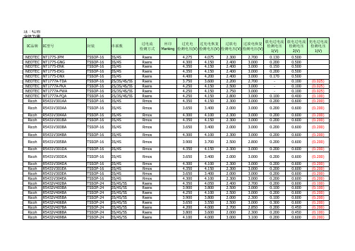
Ricoh Ricoh Ricoh Ricoh Ricoh
Ricoh
R5432V410BC R5432V412BA R5432V413BA R5432V416BA R5432V418BC
R5432V419BD
Ricoh
Ricoh Ricoh
Ricoh
R5432V420BD
R5432V501BA R5432V502BA
过电流 检测方式
Rsens Rsens Rsens Rsens Rsens Rsens Rsens Rsens Rsens Rmos
Rmos
Rmos Rmos
Rmos
Rmos
Rmos
Rmos
Rmos
Rmos Rmos Rmos Rmos Rsens Rsens Rsens Rsens Rsens Rsens Rsens Rsens
注:红色 字体为重
IC品牌 IC型号
NEOTEC NEOTEC NEOTEC NEOTEC NEOTEC NEOTEC NEOTEC NEOTEC NEOTEC
Ricoh
NT1775-JPM NT1775-GNG NT1775-ENK NT1775-EXG NT1775-DNX NT1777A-TDA NT1777A-FKA NT1777A-FWA NT1777A-FQA R5431V301AA
3S/4S/5S 3S/4S/5S 3S/4S/5S 3S/4S/5S 3S/4S/5S 3S/4S/5S
3S/4S/5S 3S/4S/5S 3S/4S/5S 3S/4S/5S
3S/4S/5S
3S/4S/5S
3S/4S/5S 3S/4S/5S 3S/4S/5S
3S/4S/5S 3S/4S/5S 3S/4S/5S 3S/4S/5S 3S/4S/5S 3S/4S/5S 3S/4S/5S 3S/4S/5S 3S/4S/5S 3S/4S/5S 3S/4S/5S 3S/4S/5S
锂电池保护IC S8204
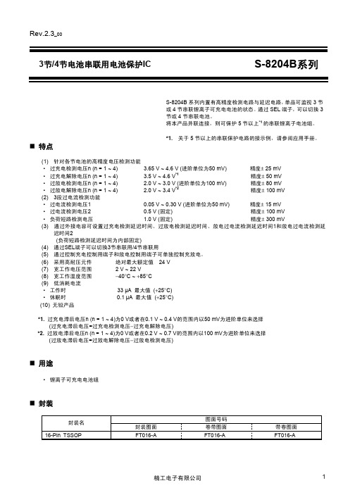
S-8204BAN-TCT1S 4.100 ± 0.025 V 4.100 ± 0.025 V 2.00 ± 0.080 V 2.50 ± 0.100 V S-8204BAO-TCT1S 3.900 ± 0.025 V 3.600 ± 0.050 V 2.50 ± 0.080 V 2.70 ± 0.100 V
过放电 解除电压 [VDU]
2.70 ± 0.100 V 3.00 ± 0.100 V
S-8204BAD-TCT1S 3.800 ± 0.025 V 3.600 ± 0.050 V 2.00 ± 0.080 V 2.30 ± 0.100 V S-8204BAE-TCT1S 4.350 ± 0.025 V 4.150 ± 0.050 V 2.50 ± 0.080 V 3.00 ± 0.100 V
(除特殊注明以外: Ta = 25 °C)
S-8204BAF-TCT1S 4.350 ± 0.025 V 4.150 ± 0.050 V 2.30 ± 0.080 V 3.00 ± 0.100 V S-8204BAG-TCT1S 4.350 ± 0.025 V 4.150 ± 0.050 V 2.80 ± 0.080 V 3.30 ± 0.100 V
S-8204BAH-TCT1S 4.200 ± 0.025 V 4.000 ± 0.050 V 2.60 ± 0.080 V 3.00 ± 0.100 V S-8204BAI-TCT1S 3.900 ± 0.025 V 3.800 ± 0.050 V 2.00 ± 0.080 V 2.00 ± 0.080 V
S-8204BAZ-TCT1S 4.250 ± 0.025 V 4.100 ± 0.050 V 3.00 ± 0.080 V 3.30 ± 0.100 V
IGBT
STGW40N120KD
STGW40NC60WD
FGH60N60UFDTU
FSAM15SM60A
STGY50NC60WD
HGTG27N120BN
IRG4PC30FDPBF
IRGP4066DPBF
HGTG40N60A4
STGD7NC60HT4
STGW20NC60VD
FGA25N120ANTDTU
2SC0435T2A0-17
STGF7NB60SL
FNA41560
STGW60H65F
STGB20NC60V
STGIPL14K60
STGW35NC120HD
HGTP10N120BN
STGIPS14K60T
IRG7PH46UDPBF
IRG4RC10UTRPBF
IRGP4062DPBF
FGPF4533
SKW15N60
IRG7I313UPBF
IRG4PC40UD-EPBF
FGH80N60FD2TU
IRG4PC30FPBF
STGP18N40LZ
IRG7PH42U-EP
IRGP4066-EPBF
HGTG10N120BND
IRGP4063DPBF
FGH75N60UFTU
STGD10NC60KT4
STGIPL20K60
STGIPS20K60
STGWA45HF60WDI
FGL60N100BNTD
STGD18N40LZT4
STGIPS10K60T
IRG7PH42UPBF
HGTG30N60A4
STGW45HF60WD
SinOne SC92F844XB 超高速1T 8051内核工业级Flash微控制器说明书
超高速1T 8051内核Flash MCU ,1 Kbytes SRAM ,16 Kbytes Flash ,128 bytes 独立EEPROM ,31通道可低功耗双模触控电路,12位ADC ,1个模拟比较器,LCD/LED Driver ,12位PWM ,3个定时器,乘除法器,UART ,SSI ,Check Sum 校验模块Page 1 of 105 V0.1SinOneSC92F8447B/8446B/8445B1 总体描述SC92F8447B/8446B/8445B (以下简称SC92F844XB )系列是一颗增强型的超高速1T 8051内核工业级Flash 微控制器,指令系统完全兼容传统8051产品系列。
SC92F844XB 集成有16 Kbytes Flash ROM 、1 Kbytes SRAM 、128 bytes EEPROM 、内置有31路高灵敏度隔空电容触控电路、最多46个 GP I/O 、16个IO 可外部中断、3个16位定时器、17路12位高精度ADC 、1个模拟比较器、8路12位PWM 、IO 驱动分级控制(LED segment 口)、1个16 ×16位硬件乘除法器、内部±1%高精度高频16/8/4/1.33MHz 振荡器和±4%精度低频128K 振荡器、可外接晶体振荡器、UART 等通讯接口等资源。
为提高可靠性及简化客户电路,SC92F844XB 内部也集成有4级可选电压LVR 、2.4V 基准ADC 参考电压、低耗电WDT 等高可靠电路。
SC92F844XB 具有非常优异的抗干扰性能,非常适合应用于各种物联网控制、大小智能家电和智能家居、充电器、电源、航模、对讲机、无线通讯、游戏机等工业控制和消费应用领域。
2 主要功能工作电压:2.4V~5.5V工作温度:-40 ~ 85℃ 封装:SC92F8447B (LQFP48) SC92F8446B (LQFP44) SC92F8445B (LQFP32)内核:超高速的单字节指令 1T 8051Flash ROM :16 Kbytes Flash ROM (MOVC 禁止寻址0000H~00FFH 的256 bytes )IAP :可code option 成0K 、0.5K 、1K 或16KEEPROM :128 bytes ,无需擦除,10万次写入,10年以上保存寿命SRAM :内部256 bytes+外部768 bytes+PWM&LCD RAM 44 bytes系统时钟(f SYS ): ● 内建高频 16MHz 振荡器(f HRC )● IC 工作的系统时钟,可通过编程器选择设定为:⏹ *********~5.5V⏹8/4/***********~5.5V●频率误差:跨越 (3.0V~5.5V) 及 (-20 ~ 85℃) 应用环境,不超过 ±1%内置低频晶体振荡器电路: ● 可外接32K 振荡器,作为Base Timer 时钟源,可唤醒STOP内建低频 128kHz LRC 振荡器:● 可作为BaseTimer 的时钟源,并唤醒STOP ● 可作为WDT 的时钟源●频率误差: 跨越 (4.0V ~ 5.5V) 及 (-20 ~ 85℃),频率误差不超过 ±4%低电压复位(LVR ): ● 复位电压有4级可选: 4.3V 、3.7V 、2.9V 、2.3V● 缺省值为用户烧写Code Option 所选值Flash 烧写和仿真: ● 2线JTAG 烧写和仿真接口。
自控专业工程设计用标准及规范

自控专业工程设计用标准及规范!自控专业工程设计用标准及规范1 行业法规及管理规定1.1 化工厂初步设计内容深度规定[(88)化基设字第251号]1.2 化工厂初步设计内容深度规定中有关内容更改的补充[(92)化基发字第695号]1.3 自控专业施工图设计内容深度规定(HG 20506)1.4 化工装置自控工程设计规定(HG/T 20636~20639)1.4.1 自控专业设计管理规定(HG/T 20636)1 自控专业的职责范围(HG/T 20636.1)2 自控专业与工艺、系统专业的设计条件关系(HG/T 20636.2)3 自控专业与管道专业的设计分工(HG/T 20636.3)4 自控专业与电气专业的设计分工(HG/T 20636.4)5 自控专业与电信、机泵及安全(消防)专业的设计分工(HG/T 20636.5)6 自控专业工程设计的任务(HG/T 20636.6)7 自控专业工程设计的程序(HG/T 20636.7)8 自控专业工程设计质量保证程序(HG/T 20636.8)9 自控专业工程设计文件校审提要(HG/T 20636.9)10 自控专业工程设计文件的控制程序(HG/T 20636.10)1.4.2 自控专业工程设计文件的编制规定(HG/T 20637)1 自控专业工程设计文件的组成和编制(HG/T 20637.1)2 自控专业工程设计用图形符号和文字代号(HG/T 20637.2)3 仪表设计规定的编制(HG/T 20637.3)4 仪表施工安装要求的编制(HG/T 20637.4)5 仪表请购单的编制(HG/T 20637.5)6 仪表技术说明书的编制(HG/T 20637.6)7 仪表安装材料的统计(HG/T 20637.7)8 仪表辅助设备及电缆、管缆的编号(HG/T 20637.8)1.4.3 自控专业工程设计文件的深度规定(HG/T 20638)1.4.4 自控专业工程设计用典型图表及标准目录(HG/T 20639)1 自控专业工程设计用典型表格(HG/T 20639.1)2 自控专业工程设计用典型条件表(HG/T 20639.2)3 自控专业工程设计用标准目录(HG/T 20639.3)1.5 化工装置工艺系统工程设计规定(HG 20557-20559)1.5.1 工艺系统设计管理规定(HG 20557)1.5.2 工艺系统设计文件内容的规定(HG 20558)1.5.3 管道仪表流程图设计规定(HG 20559)1.6 石油化工装置基础设计(初步设计)内容规定(SHSG-033)1.7 石油化工自控专业工程设计施工图深度导则(SHB-Z01)2 图形符号2.1 过程检测和控制流程图用图形符号和文字代号(GB 2625)2.2 过程检测和控制系统用文字代号和图形符号(HG 20505)2.3 Instrumentation Symbols and Identification 仪表符号和标志[SHB-Z02 (等同于ISA S5.1)]2.4 Binary Logic Diagrams for Process Operations用于过程操作的二进制逻辑图[SHB-Z03 (等同于ISA S5.2)]2.5 Graphic Symbols for Distributed Control/Shared Display Instrumentation, Logic and Computer Systems 分散控制/共用显示仪表、逻辑和计算机系统用图形符号[SHB-Z04 (等同于ISA S5.3)]2.6 Instrument Loop Diagrams仪表回路图图形[SHB-Z05 (等同于ISA S5.4)]2.7 Graphic Symbols for Process Displays (ISA S5.5) 过程显示图形符号2.8 分散型控制系统硬件设备的图形符号(JB/T5539)2.9 Process Measurement Control Function and Instrumentation-Symbolic Representation (ISO 3511)过程测量控制功能及仪表符号说明2.10 Recommended Graphical Symbols Part 15: Binary Logic Elements (IEC 117-15)推荐的图形符号:二进制逻辑元件2.11 Graphic Symbols for Logic Diagrams (two state devices) (ANSI Y32.14)逻辑图用图形符号(二状态元件) 2.12 Symbolic Representation for Process Measurement Control Functions and Instrumentation (BS 1646)过程测量控制功能及仪表用符号说明2.13 Bildzeichen fü r messen, steuern, regeln: Allgemeine bildzeichen. 自控图例:一般图形 (DIN 19228)2.14 仪表符号 (JIS Z8204)3 工程设计规范3.1 计算站场地技术要求(GB 2887)3.2 计算机机房用活动地板技术条件(GB 6650 )3.3 城乡燃气设计规范(GB 50028)3.4 氧气站设计规范(GB 50030)3.5 乙炔站设计规范(GB 50031)3.6 工业企业照明设计标准(GB 50034)3.7 锅炉房设计规范(GB 50041)3.8 小型火力发电厂设计规范(GB 50049)3.9 电子计算机机房设计规定(GB 50174)3.10 氢气站设计规范(GB 50177)3.11 压缩空气站设计规范(GBJ 29)3.12 冷库设计规范(GBJ 72)3.13 洁净厂房设计规范(GBJ 73)3.14 石油库设计规范(GBJ 74)3.15 工业用软水除盐设计规范(GBJ 109)3.16 工业电视系统工程设计规范(GBJ 115)3.17 化工厂控制室建筑设计规范(HG 20556)3.18 石油化工储运系统罐区设计规范(SH3007)3.19 炼油厂燃料油燃气锅炉房设计技术规定(SHJ 1026)3.20 加油站建设规定(SHQ1)4 自动化仪表4.1 工业自动化仪表电源、电压(GB 3368)4.2 不间断电源设备(GB 7260)4.3 工业自动化仪表用模拟气动信号(GB 777)4.4 工业自动化仪表用模拟直流电流信号(GB 3369)4.5 工业过程测量和控制系统用电动和气动模拟记录仪和指示仪性能测定方法(GB 3386)4.6 工业过程测量和控制用检测仪表和显示仪表精度等级(GB/T 13283)4.7 工业自动化仪表用气源压力范围和质量(GB 4830)4.8 工业自动化仪表工作条件温度和大气压(ZBY 120)4.9 工业自动化仪表电磁干扰电流畸变影响试验方法(ZBY 092)4.10 工业自动化仪表工作条件~振动(GB 4439)4.11 工业自动化仪表盘基本尺寸及型式(GB 7353)4.12 工业自动化仪表盘盘面布置图绘制方法(JB/T 1396)4.13 工业自动化仪表盘接线接管图的绘制方法(JB/T 1397)4.14 工业自动化仪表公称通径值系列(ZBN 10004)4.15 工业自动化仪表工作压力值系列(ZBN 10005)4.16 流量测量仪表基本参数(GB 1314)4.17 工业自动化仪表通用试验方法-接地影响(ZBN 10003.26)4.18 Quality Standard for Instrument Air (ISA S7.3)仪表空气的质量标准5 自控专业工程设计规范5.1 流量测量节流装置用孔板、喷嘴和文丘里测量充满圆管的流体流量(GB/T 2624 等同于ISA 5167)5.2 自动化仪表选型规定(HG 20507)5.3 控制室设计规定(HG 20508)5.4 仪表供电设计规定(HG 20509)5.5 仪表供气设计规定(HG 20510)5.6 信号报警联锁系统设计规定(HG 20511)5.7 仪表配管配线设计规定(HG 20512)5.8 仪表系统接地设计规定(HG 20513)5.9 仪表及管线伴热和绝热保温设计规定(HG 20514)5.10 仪表隔离和吹洗设计规定(HG 20515)5.11 自动分析器室设计规定(HG 20516)5.12 分散控制系统工程设计规定(HG/T 20573)5.13 自控设计常用名词术语5.14 石油化工自动化仪表选型设计规范(SH 3005)5.15 石油化工控制室和自动分析器室设计规范(SH 3006)5.16 石油化工仪表配管配线设计规范(SH 3019)5.17 石油化工仪表接地设计规范(SH 3081)5.18 石油化工仪表供电设计规范(SH 3082)5.19 石油化工分散控制系统设计规范(SH/T 3092)5.20 石油化工企业信号报警、联锁系统设计规范(SHJ 18)5.21 石油化工企业仪表供气设计规范(SHJ 20)5.22 石油化工仪表保温及隔离吹洗设计规范(SH 3021)5.23 石油化工紧急停车及安全联锁设计导则(SHB-Z06)5.24 Environmental Conditions for Process Measurement and Control Systems: Temperature and Humidity 过程测量和控制系统的环境条件:温度和湿度(ISA S71.01)5.25 Control Centers Facilities (ISA RP60.1) 控制中心设施5.26 Human Engineering for Control Centers (ISA RP60.3) 控制中心的人类工程5.27 Documentation for Control Centers (ISA RP60.4) 控制中心的文件5.28 Electrical Guide for Control Centers (ISA RP60.8)控制中心的电气导则5.29 Piping Guide for Control Centers (ISA RP60.9) 控制中心的配管导则5.30 Recommended Practice for the Design and Installation of Pressure-Relieving Systems in Refineries (API RP 520)炼油厂压力泄压系统的设计和安装5.31 Vibration, Axial Position, and Bearing Temperature Monitoring Systems.(API 670)非接触式振动和轴位移监测系统5.32 Control Valve Sizing Equations for Incompressible Fluids (ISA S39.1) 不可压缩流体用调节阀的口径计算公式5.33 Flow Equations for Sizing Control Valves (ISA S75.01)控制阀口径计算公式5.34 Control Valve Terminology (ISA S75.05 )控制阀术语5.35 Control Valve Manifold Designs (ISA RP75.06)控制阀的阀组设计5.36 调节阀口径计算(ANSI FCI62-1)5.37 Control Valve Seat Leakage (ANSI B16.104/FCI70-2)控制阀泄漏量规定5.38 Terminology for Automatic Control (ANSI C85.1) 自动控制术语6 通用图册和设计手册6.1 自控安装图册(HG/T 21581)6.2 仪表单元接线接管图册(TC 50B1)6.3 仪表回路接线图册(TC 50B2)6.4 自控设计防腐蚀手册(CADC 051)6.5 仪表修理车间设计手册(CADC 052)6.6 石油化工企业仪表修理车间设计导则(SHB-Z002)6.7 仪表维护设备选用手册(SHB-Z003)6.8 Manual on Installation of Refinery Instruments and Control systems (API RP550) 炼油厂仪表及调节系统安装手册6.9 Part Ⅱ Installation Operation and Maintenance of Combustible Gas Detection Instruments (ISA S12.13) 可燃气体检测仪表的安装、操作和维护7 管法兰与管螺纹7.1 钢制管法兰国家标准汇编(GB 9112~9128)7.2 钢制管法兰、垫片、紧固件(HG 20592~20635~97)7.3 高压管、管件及紧固件通用设计(H1~37)7.4 石油化工企业钢制管法兰(SH 3406)7.5 管路法兰及垫片(JB/T 74~90)7.6 用螺纹密封的管螺纹(GB 7306,相应于55°圆锥管螺纹)7.7 非螺纹密封的管螺纹(GB 7307,相应于55°圆柱管螺纹)7.8 60°圆锥管螺纹(GB/T 12716)7.9 钢管螺纹[ISO 7/1 (R.RC)]7.10 直管螺纹[ISO 228/1 (G.Ga)]7.11 Pipe Flanges and Falanged Fittings Flange surface shall be smooth. (ANSI B16.5)管法兰和法兰连接件7.12 Steel Orifice Flanges (ANSI B16.36、B16.36a)钢制孔板法兰7.13 Flange Mounted Sharp Edged Orifice Plates for Flow Measurement (ISA RP3.2)流量测量用法兰安装式锐孔板7.14 管螺纹(ASME B1.20.1)8 安全8.1 爆炸性环境用防爆电气设备(GB 3836)8.2 外壳防护等级的分类(GB 4208)8.3 电气设备安全设计导则(GB 4064)8.4 电子测量仪器安全要求(GB 4793)8.5 爆炸和火灾危险环境电力设计规范(GB 50058)8.6 石油化工企业设计防火规范(GB 50160)及1999年筑物抗震设计8.7 构筑物抗震设计规范(GB 50191)8.8 建筑抗震设计规范(GBJ 11)8.9 建筑设计防火规范(GBJ 16)8.10 火灾自动报警系统设计规范(GBJ 116)8.11 化工企业爆炸和火灾危险环境电力设计规范(HGJ 21)8.12 化工企业静电接地设计规程(HGJ 28)8.13 石油化工企业可燃气体和有毒气体检测报警设计规范(SH 3063)8.14 Electrical Instrument in Hazardous Atmospheres (ISA RP12.1) 危险大气里的电气仪表8.15 Instrument Purging for Reduction of Hazardous Area Classification (ISA S12.4) 用于降低危险区域等级的仪表吹气法8.16 Installation of Intrinsically safe Systems for Hazardous (Classified) Locations (ISA RP12.6) 本安系统在危险区的安装8.17 Area Classification in Hazardous (Classified) Dust Locations (ISA S12.10) 危险粉尘场所的区域分类8.18 Electrical Equipment for Use in Class1, Division 2 Hazardous (Classified) Locations (ISA S12.12) 1区2类危险场所的电气设备8.19 Classification of Degrees of Protection Provided by Enclosures. (IEC 529) 外壳防护标准8.20 Electrical apparatus for explosive gas atmospheres part10: Classification of hazardous areas.(IEC 79-10)爆炸气体场所的电力设备第10部分:危险场所的划分8.21 Part14: Electrical installations in explosive gas atmospheres.(IEC 79-14)爆炸气体环境的电力设备(除矿用外)8.22 Intrinsically Safe Apparatus in Division I Hazardous Locations (NFPA 493) I区危险场所中的本安设备8.23 Classification of Areas for Electrical Installations in Petroleum Refineries (API RP500A)炼油厂电气安装用防爆场所的划分9 环境卫生9.1 密封放射源一般规定(GB 4076)9.2 放射卫生防护基本标准(GB 4792)9.3 电磁辐射防护规定(GB 8702)9.4 辐射防护规定(GB 8703)9.5 放射性物质安全运输规定(GB 11806)9.6 低、中水平放射性固体废物暂时贮存规定(GB 11928)9.7 操作开放型放射性物质的辐射防护规定(GB 11930)9.8 环境核辐射监测规定(GB 12379)9.9 放射性防护规范(GBJ 211)9.10 a 、g 射线外照射个人剂量监测规定(EJ 269)9.11 工业噪声控制设计规范(GBJ 87)9.12 工业企业噪声测量规定(GBJ 122)9.13 化工建设项目噪声控制设计规定(HG 20503)9.14 石油化工企业环境保护设计规范(SHJ 24)9.15 炼油厂卫生防护距离(SHJ 1070)9.16 Methods for the Measurement of Sound Pressure Levels (ANSI S1.13)声压级的测量方法9.17 石油化工企业职业安全卫生设计规范(SH3047)10 施工验收10.1 工业自动化仪表工程施工及验收规范(GBJ 93)10.2 自动化仪表安装工程质量检验评定标准(GBJ 131)10.3 电气装置安装工程接地装置施工及验收规范(GB 50169)10.4 电气装置安装工程低压电器施工及验收规范(GB 50254)10.5 洁净室施工及验收规范(HGJ 71)10.6 石油化工仪表工程施工技术规程(SH3521)10.7 长输管道仪表工程施工及验收规范(SYJ 4005)10.8 工业控制计算机系统验收大纲(JB/T 5234)附录A 标准代号对照表A.1 GB(GB/T) 中华人民共和国国家标准A.2 JB(JB/T) 机械工业部行业标准A.3 HG(HG/T) 化学工业部行业标准A.4 HGJ 化学工业部工程建设标准A.5 H 原化学工业部标准A.6 CD 原化学工业部基本建设局标准A.7 TC(CADC) 化学工业部自动控制设计技术中心站标准A.8 SH 中国石化总公司行业标准A.9 SHJ(SYJ) 中国石化总公司工程建设标准A.10 SHB- Z 中国石化总公司自动控制设计技术中心站标准A.11 SYJ 中国石油天然气工业总公司工程建设标准A.12 NDGJ 电力工业部工程建设标准A.13 JGJ 建设部工程建设标准A.14 FJJ 纺织总会工程建设标准A.15 EJ 中国核工业总公司行业标准A.16 JJG 国家计量总局标准A.17 ZBY 仪器仪表专业标准A.18 ZBN 仪器仪表行业标准A.19 JB/YQ 仪器仪表行业内部标准A.20 ISO 国际标准化组织 INTERNATIONAL ORGANIZITION FOR STANDARDIZA TIONA.21 IEC 国际电工委员会 INTERNATIONAL ELECTROTECHNICAL COMMISIONA.22 ISA 美国仪表协会 INSTRUMENT SOCIETY OF AMERICAA.23 API 美国石油学会 AMERICAN PETROLEUM INSTITUTEA.24 ANSI 美国国家标准协会 AMERICAN NATIONAL STANDARDS INSTITUTEA.25 ASME 美国机械工程师协会 AMERICAN SOCIETY OF MECHANICAL ENGINEERSA.26 NEPA 美国国家防火协会、美国流体动力协会 NATIONAL FIRE PROTECTION ASSOCIATION A.27 NEC 美国国家电气规程 NATIONAL ELECTRICAL CODEA.28 NEMA 美国电气制造商协会 NATIONAL ELECTRICAL MANUFACTURES ASSOCIATIONA.29 DIN 德国国家标准 DEUTSCHE INDUSTRIE NORMA.30 BS 英国国家标准 BRITISH STANDARDSA.31 JIS 日本国家标准 JAPANESE INDUSTRIAL STANDARDS。
TTP控制器
AS8202BTTP-C2NF Communication Controller1 General DescriptionThe AS8202B communication controller is an integrated device supporting serial communication according to the TTP specification version 1.1. It performs all communication tasks such as reception and transmission of messages in a TTP cluster without interaction of the host CPU. TTP provides mechanisms that allow the deployment in high-dependability distributed real-time systems. It provides the following services:⏹ Predictable transmission of messages with minimal jitter⏹ Fault-tolerant distributed clock synchronization⏹ Consistent membership service with small delay⏹ Masking of single faults2 Key Features⏹ Dual-channel controller for redundant data transfers⏹ Dedicated controller supporting TTP (time-triggered protocolclass C standardized in SAE 6003)⏹ Suited for dependable distributed real-time systems withguaranteed response time⏹ Asynchronous data rate up to 4 Mbit/s (MFM/Manchester)⏹ Synchronous data rate 20 to 25 Mbit/s⏹ Bus interface (speed, encoding) for each channel selectableindependently⏹ 40 MHz oscillator clock support⏹ 16 MHz bus guardian clock with support for 16 MHz crystal or16 MHz oscillator⏹ Single power supply 3.3V, 0.35µm CMOS process⏹ Full automotive temperature range (-40ºC to 125ºC)⏹ 16k x 16 SRAM for message, status, control area(communication network interface) and for schedulinginformation (MEDL)⏹ 4k x 16 (plus parity) instruction code RAM for protocol executioncode⏹ Datasheet conforms to protocol revision 2.05⏹ 16k x 16 instruction code ROM containing startup executioncode and deprecated protocol code revision 1.00⏹ 16-bit non-multiplexed asynchronous host CPU interface⏹ 16-bit RISC architecture⏹ Software tools, design support, development boards availableVisit ⏹ Certification support package according to RTCA/DO-254 DALA available – Visit ⏹ RoHS conform3 ApplicationsThe device is ideal for application fields such as, aerospace according to DO-254 level A (e.g. flight control, power distribution, engine control), industrial systems, and railway systems.Contents1 General Description (1)2 Key Features (1)3 Applications (1)4 Pin Assignments (3)4.1 Pin Descriptions (3)5 Absolute Maximum Ratings (6)6 Electrical Characteristics (7)7 Detailed Description (9)7.1 Host CPU Interface (9)7.1.1 Synchronous READYB Generation (12)7.2 Reset and Oscillator (13)7.2.1 External Reset Signal (13)7.2.2 Integrated Power-On Reset (13)7.2.3 Oscillator Circuitry (13)7.2.4 Built-in Characteristics (14)7.3 TTP Bus Interface (14)7.4 TTP Asynchronous Bus Interface (15)7.5 TTP Synchronous Bus Interface (15)7.6 Test Interface (16)7.7 LED Signals (16)8 Package Drawings and Markings (17)9 Ordering Information (19)4 Pin Assignments4.1 Pin DescriptionsTable 1. Pin DescriptionsPin Name Pin Number Dir DescriptionVDD4, 12, 29, 49, 59, 74Power pin Positive Power SupplyVSS13, 30, 41, 50, 60,75, 80Negative Power SupplyVDDBG70Positive Power Supply for Bus Guardian (connect to VDD) VSSBG73Negative Power Supply for Bus Guardian (connect to VSS)RAM_CLK_TESTSE21TTL Input with internal weak pull-downRAM_CLK when STEST=0 and USE_RAM_CLK=1, else Test Input, connect to VSS if not usedSTEST 22Test Input, connect to VSSFTEST 24Test Input, connect to VSSFIDIS 25Test Input, connect to VSSTTEST 61TTL Input with internal weak pull-upTest Input, connect to VDDUSE_RAM_CLK34TTL Input with internal weak pull-downRAM_CLK Pin Enable, connect to VSS if not usedXIN02Analog CMOS pinMain Clock: 40MHz external clock input CTEST 3Test input, to be unconnectedOSCMODE 23TTL Input with internal weak pull-downConnect to VDD 1XIN172Analog CMOS pinBus Guardian Clock: Analog CMOS Oscillator Input, use as input when providing external clockXOUT171Bus Guardian Clock: Analog CMOS Oscillator Output, leave open when providing external clockRESETB 26TTL Input with internal weak pull-up Main Reset Input, active lowTxD05TTL output with internal weak pull-up at tristate TTP Bus Channel 0: Transmit DataCTS06TTL output with internal weak pull-down at tristate TTP Bus Channel 0: Transmit EnableRxD011TTL Input with internal weak pull-upTTP Bus Channel 0: Receive DataTxCLK07TTL Input with internal weak pull-down TTP Bus Channel 0: Transmit Clock (MII mode)RxER08TTL Input with internal weak pull-up TTP Bus Channel 0: Receive Error (MII mode)RxCLK09TTL Input with internal weak pull-down TTP Bus Channel 0: Receive Clock (MII mode)RxDV010TTL Input with internal weak pull-up TTP Bus Channel 0: Receive Data Valid (MII mode)TxD114TTL output with internal weak pull-up at tristate TTP Bus Channel 1: Transmit DataCTS115TTL output with internal weak pull-down at tristate TTP Bus Channel 1: Transmit EnableRxD120TTL Input with internal weak pull-upTTP Bus Channel 1: Receive DataTxCLK116TTL Input with internal weak pull-down TTP Bus Channel 1: Transmit Clock (MII mode)RXER117TTL Input with internal weak pull-up TTP Bus Channel 1: Receive Error (MII mode)RXCLK118TTL Input with internal weak pull-down TTP Bus Channel 1: Receive Clock (MII mode)RxDV119TTL Input with internal weak pull-upTTP Bus Channel 1: Receive Data Valid (MII mode)Table 1. Pin DescriptionsPin Name Pin NumberDirDescriptionA[11:0]48-42, 39-35TTL InputHost Interface (CNI) Address Bus2D[15:0]69-62, 58-51TTL input/output with tristate Host Interface (CNI) Data Bus, tristateCEB 76TTL Input with internal weak pull-upHost Interface (CNI) chip enable, active lowOEB 77Host interface (CNI) output enable, active lowWEB 78Host interface (CNI) write enable, active lowREADYB 79TTL output with internal weak pull-up at tristateHost interface (CNI) transfer finish signal, active low, opendrain3INTB 28Host interface (CNI) time signal (interrupt), active low, open drain LED[2:0]33-31TTL output with internal weak pull-down at tristateConfigurable generic output portNC1, 27, 40Not connected, leave open1.This pin selects a clock multiplier of 1. This is the only supported operation mode.2.The device is addressed at 16-bit data word boundaries. If the device is connected to a CPU with a byte-granular address bus, remem-ber that A[11:0] of the AS8202B device has to be connected to A[12:1] of the CPU (considering a little endian CPU address bus)3.At de-assertion READYB is driven to the inactive value (high) for a configurable time.Table 1. Pin DescriptionsPin Name Pin Number Dir DescriptionDatasheet - A b s o lu t e M a x im u m R a ti n gs5 Absolute Maximum RatingsStresses beyond those listed in Table 2 may cause permanent damage to the device. These are stress ratings only. Functional operation of the device at these or any other conditions beyond those indicated in Electrical Characteristics on page 7 is not implied. Exposure to absolute maximum rating conditions for extended periods may affect device reliability.Table 2. Absolute Maximum RatingsSymbol Parameter Min Max Unit NotesElectrical ParametersV DD DC Supply voltage-0.3 5.0VV IN Input voltage-0.3V DD+0.3V any pinI IN Input current-100100mA any pin, T AMB=25ºC Electrostatic DischargeESD Electrostatic discharge1000V HBM: 1KV Mil.std.883, Method 3015.7 Temperature Ranges and Storage ConditionsT STRG Storage temperature-55+150ºCT BODY Package body temperature260ºC The reflow peak soldering temperature (body temperature) specified is in accordance with IPC/JEDEC J-STD-020 “Moisture/Reflow Sensitivity Classification for Non-HermeticSolid State Surface Mount Devices”. The lead finish for Pb-free leaded packages ismatte tin (100% Sn).H Humidity non-condensing585%MSL Moisture sensitivity level3Represents a maximum floor life time of 168h6 Electrical CharacteristicsT AMB= -40 to +125 ºC, V DD = 3V to +3.6V, V SS = 0V unless otherwise specified.Table 3. Electrical CharacteristicsSymbol Parameter Conditions Min Typ Max Unit Operating ConditionsI DDs Static Supply CurrentAll inputs tied to V DD/V SS,clocks stopped, exclusive of I/Odrive requirements, V DD=3.6V5900µAI DD Operating Supply Current(see note 1)VDD=3.3V,exclusive of I/O drive requirements100mACLK1Clock Period of Bus Guardian Clock(see note 1)62.5nsTTL Input Pins and TTL Bidirectional Pins in Input/Tristate ModelV IL Input Low Voltage0.8V V IH Input High Voltage 2.0VI INleak Input Leakage Current Pins without pad resistors,V DD=3.6V-11µAI IL Input Low Current Pins with pull-downresistors, V DD=3.0VV IN=0.4V4.9(see note 2)µAV IN=0.8V8.8(see note 2)Pins with pull-upresistorsV DD=3.6VV IN=0V-15-75I IH Input High Current Pins with pull-downresistorsV DD=3.6VV IN=3.6V1575µA Pins with pull-upresistors, V DD=3.0VV IN=2.0V-10.7(see note 2)V IN=2.5V-6(see note 2)C IN Input Capacitance4.5(see note2)pFRxD Pint ASYM_Rxt(V IN=0.5*V DD)Asymmetric Receiver Delay RxDT=125ºC, V DD=3.0V,C LOAD=35pF RxD[1,0]-2(see note 3)2(see note 3)nsCMOS Inputs (XIN), drive from external clock generatorDrive at XINC XIN Input Capacitance 1.9 2.5pFI XIN Input Current±1(see note 3)µA V IL_XIN Input Low Voltage00.3* V DD V V IH_XIN Input High Voltage0.7* V DD V DD V Outputs and TTL Bi-directional Pins in Output ModeI OL Output Low Current V DD=3.0V, Vo = 0.4V-4mAI OH Output High Current V DD=3.0V, Vo = 2.5V4mANotes:1. Typical values: CLK0=40 MHz (duty cycle 45-55%), CLK1=16 MHz.2. Implicitly tested.3. Guaranteed by design; not tested during production.I OZOutput Tristate CurrentV DD =3.6V±10(see note 3)µAt RISEt(V OUT =0.1*V DD )tot(V OUT =0.9*V DD )Transition Time – RiseT = 125 ºC, V DD =3.0V, C LOAD =35pFCTS[1,0], LED[2:0], INTB 8.1(see note 2)nsD[15:0], READYB 8.9(see note 2)t FALLt(V OUT =0.9*V DD )tot(V OUT =0.1*V DD )Transition Time – FallT = 125 ºC, V DD =3.0V, C LOAD =35pFCTS[1,0], LED[2:0], INTB 6(see note 2)nsD[15:0], READYB7(see note 2)TxD Pins t RISEt(V OUT =0.3*V DD )tot(V OUT =0.7*V DD )Transition Time – Rise TxDT = 125 ºC, V DD =3.0V, C LOAD =35pF TxD[1,0]4.5(see note 3)nst FALLt(V OUT =0.7*V DD )tot(V OUT =0.3*V DD )Transition Time – Fall TxD T = 125 ºC, V DD =3.0V, C LOAD =35pF TxD[1,0]3(see note 3)nst ASYM_Rxt(V OUT =0.5*V DD ) Asymmetric Driver Delay TxD T = 125 ºC, V DD =3.0V, C LOAD =35pFTxD[1,0]-3(see note 3)3(see note 3)nsTable 3. Electrical CharacteristicsSymbol Parameter Conditions Min Typ Max Unit7 Detailed DescriptionThe AS8202B is the first TTP controller to support both MFM and Manchester coding. Manchester coding is important for DC-free data transmission, which allows the use of transformers in the data stream. The AS8202B is pin-compatible with its predecessor, the AS8202. The AS8202B provides support for fault-tolerant, high-speed bus systems in a single device. The communication controller is qualified for the full temperature range required for automotive applications and is certifiable according to RTCA standards. It offers superior reliability and supports data transfer rates of 25 Mbit/s with MII and up to 4 Mbit/s with MFM/Manchester.The CNI (communication network interface) forms a temporal firewall. It de-couples the controller network from the host subsystem by use of a dual ported RAM (CNI). This prevents the propagation of control errors. The interface to the host CPU is implemented as a 16-bit wide non-multiplexed asynchronous bus interface.The TTP follows a conflict-free media access strategy called time division multiple access (TDMA). This means, TTP deploys a time slot technique based on a global time that is permanently synchronized. Each node is assigned a time slot in which it is allowed to perform transmit operation. The sequence of time slots is called TDMA round, a set of TDMA rounds forms a cluster cycle. The operation of the network is repeated after one cluster cycle. The sequence of interactions forming the cluster cycle is defined in a static time schedule, called message descriptor list (MEDL). The definition of the MEDL in conjunction with the global time determines the response time for a service request.The membership of all nodes in the network is evaluated by the communications controller. This information is presented to all correct cluster members in a consistent fashion. During operation, the status of all other nodes is propagated within one TDMA round. Please read more about TTP and request the TTP specification at .7.1 Host CPU InterfaceThe host CPU interface, also referred to as CNI (Communication Network Interface), connects the application circuitry to the AS8202B TTP controller. All related signal pins provide an asynchronous read/write access to a dual ported RAM located in the AS8202B. There are no setup/ hold constraints referring to the microtick (main clock “CLK0”).All accesses have to be executed on a granularity of 16-bit (2 byte), the device does not support byte-wide accesses. The pin A0 (LSB) of the device differentiates even and odd 16-bit word addresses and is typically connected to A1 of a little-endian host CPU. The A0 of host CPU is not connected to the device, and the application/driver on the host CPU should force all accesses to be 16-bit. For efficiency reasons, the host CPU application/driver may access some memory locations of the AS8202B using wider accesses (e.g. 32-bit), and the bus interface of the host CPU will automatically split the access into two consecutive 16-bit wide accesses to the TTP controller. Note that particularly in such a setup all timing parameters of the host CPU interface must be met, especially the inactivity timeouts described as symbols 16–19.The host interface features an interrupt or time signal INTB to notify the application circuitry of programmed and protocol-specific, synchronous and asynchronous events.The host CPU interface allows access to the internal instruction code memory. This is required for proper loading of the protocol execution code into the internal instruction code RAM, for extensive testing of the instruction code RAM and for verifying the instruction code ROM contents. INTB is an open-drain output, i.e. the output is only driven to '0' and is weak-pull-up at any other time, so external pull-up resistors or transistors may be necessary depending on the application.READYB is also an open-drain output, but with a possibility to be driven to ‘1’ for a defined time (selectable by register) before weak-pull-up at any other time.The LED port is software-configurable to automatically show some protocol-related states and events, see below for the LED port configuration. Table 4. Host Interface PortsPin Name Mode Width CommentA[11:0]in12CNI address bus, 12-bit (A0 is LSB)D[15:0]inout (tri)16CNI data bus, 16-bit (D0 is LSB)CEB in1CNI chip enable, active lowWEB in1CNI write enable, active lowOEB In1CNI output enable, active lowREADYB out (open drain)1CNI ready, active lowINTB out (open drain)1CNI interrupt, time signal, active low RAM_CLK_TESTSE in1HOST clockUSE_RAM_CLK in1HOST clock pin enableAsynchronous READYB permits the shortest possible bus cycle but eventually requires signal synchronization in the application. Connect USE_RAM_CLK to VSS to enable this mode of operation.Synchronous READYB uses an external clock (usually the host processor’s bus clock) for synchronization of the signal, eliminating external synchronization logic. Connect USE_RAM_CLK to VDD and RAM_CLK_TESTSE to the host processor's bus clock to enable this mode of operation.Note:Due to possible metastability occurrence, it is not recommended to be used in safety critical systems.Table 5. Asynchronous DPRAM InterfaceSymbol Parameter Conditions Min Typ Max Units Tc Controller Cycle Time25ns1aInput Valid to CEB, WEB (Setup Time)A[11:0]5ns2a D[15:0]1bCEB, WEB to Input Invalid (Hold Time)A[11:0]3ns2b D[15:0]43Input Rising to CEB, WEB Falling CEB, WEB, OEB5(see note 1)ns4CEB, WEB Rising to Input Falling CEB, WEB, OEB5(see note 1,2)ns5Write Access Time (CEB, WEB toREADYB)Min = 1 Tc, Max = 4 Tc25100ns6CEB, WEB de-asserted to READYBde-asserted9.4ns 7a Input Valid to CEB, OEB (Setup Time)A[11:0]5ns 7b CEB, OEB to Input Invalid (Hold Time)A[11:0]2ns8Input Rising to CEB, OEB Falling CEB, WEB, OEB5(see note 1)ns9CEB, OEB Rising to Input Falling CEB, WEB, OEB5(see note 1)ns10Read Access Time (CEB, OEB toREADYB)Min = 1.5 Tc, Max = 8 Tc37.5200ns 11a CEB, OEB asserted to signal asserted D[15:0] 4.08.4ns11b CEB, OEB de-asserted to signal de-asserted D[15:0] 3.88ns11c READYB8.812READYB, D skew±2ns13RAM_CLK_TESTSE Rising toREADYB Falling USE_RAM_CLK=1 3.713.5ns14RAM_CLK_TESTSE Rising toREADYB Rising USE_RAM_CLK=139.7ns15RAM_CLK_TESTSE Rising toREADYB Deactivated 1->Z USE_RAM_CLK=1Readydelay=00 3.612.9nsReadydelay=01 4.515.4Readydelay=10 5.418.8Readydelay=11 6.422.216Read to Read Access Inactivity Time(CEB, OEB low to CEB, OEB low)Min = 1.5 Tc37.5(see note 1)nsNotes:1. Prior to starting a read or write access, CEB, WEB and OEB have to be stable for at least 5 ns (see symbol 3, 4, 8, 9). In addition the designer has to consider the minimum inactivity time according to symbols 16, 17, 18, 19. For more information on the inactivity times (see Figure 3).2. To allow proper internal initialization, after finishing any write access (CEB or WEB is high) to the internal CONTROLLER_ON register, CEB OEB and WEB have to be stable high within 200 ns (min = 8 Tc).3. All values not tested during production, guaranteed by design.Figure 3. Read/Write Access Inactivity Time17Read to Write Access Inactivity Time (CEB, OEB low to CEB, WEB low)5(see note 1)ns 18Write to Write Access Inactivity Time (CEB, WEB low to CEB, WEB low)5(see note 1,2)ns 19Write to Read Access Inactivity Time (CEB, WEB low to CEB, OEB low)5(see note 1,2)nsTable 5. Asynchronous DPRAM InterfaceSymbol ParameterConditionsMin Typ Max UnitsFigure 5. Write Access Timing (WEB Controlled)Figure 6. Read Access Timing (CEB Controlled)Figure 7. Read Access Timing (OEB Controlled)7.1.1 Synchronous READYB GenerationSynchronous READYB is aligned to host clock (with pulse duration of one host clock cycle) to fulfill the required host timing constraints for input setup and input hold time to/after host clock rising edge.Note:Connect USE_RAM_CLK to VDD and RAM_CLK_TESTSE to the host processor's bus clock to enable this mode of operation. Due topossible metastability occurrence, it is not recommended to be used in safety critical systems.7.2 Reset and Oscillator7.2.1 External Reset SignalTo issue a reset of the chip the RESETB port has to be driven low for at least 1µs. Pulses under 50ns duration are discarded. At power-up the reset must overlap the build-up time of the power supply. This reset may only be used if a proper power-on reset can be ensured (refer to Section 7.2.2 Integrated Power-On Reset).7.2.2 Integrated Power-On ResetThe device has an internal Power-On-Reset generator. When supply voltage ramps up, the internal reset signal is kept active (low) for 33µs typical.Note:In case of non-compliance keep the external reset (RESETB) active for min. 5 ms after supply voltage is valid and main clock is stable.7.2.3 Oscillator CircuitryThe main clock requires an external oscillator. The bus guardian requires an external oscillator or an external quartz.Figure 9. Main Clock SetupXIN0 of the main clock shall be supplied by a 40MHz clock provided by an oscillator IC.Table 6. Pin ModePin Name Mode CommentXIN1analog Bus guardian oscillator input (external clock input)RESETBinExternal resetTable 7. ParametersSymbol Parameter Min Typ Max Unit dV/dt supply voltage slope551--V/ms tporespower on reset active time after VDD > 1,0V253349µsExternal oscillator 40MHz square waveX I N OFigure 10. Bus Guardian Clock SetupThe bus guardian clock (XIN1/XOUT1) supports driving a quartz crystal oscillation, as well as a clock input by an external oscillator.7.2.4 Built-in Characteristics7.3 TTP Bus InterfaceThe AS8202B contains two TTP bus units, one for each TTP channel, building the TTP bus interface. Each TTP bus channel contains atransmitter and a receiver and can be configured to be either in the asynchronous or synchronous mode of operation. Note that the two channels (channel 0 and channel 1) can be configured independently for either of these modes.The drivers of the TxD and CTS pins are actively driven only during a transmission window, all the other time the drivers are switched off and the weak pull resistors are active. External pull resistors must be used to define the signal levels during idle phases.Note:The transmission window may be different for each channel.Table 8. CharacteristicsSymbol Pin Parameter MinTypMax Unit Note Tosc_startup1XIN1/XOUT1Oscillator startup time (Bus Guardian clock)20msFrequency: 16MHzTable 9. Bus Interface ConnectionsPin Name Tx inactive TxD[0]weak pull-up CTS[0]weak pull-down TxD[1]weak pull-up CTS[1]weak pull-down7.4 TTP Asynchronous Bus InterfaceWhen in asynchronous mode of operation the channel's bus unit uses a self-clocking transmission encoding which can be either MFM orManchester at a maximum data rate of 4 Mbit/s on a shared media (physical bus). The pins can either be connected to drivers using recessive/dominant states on the wire as well as drivers using active push/pull functionality.The RxD signal uses '1' as the inactivity level. In the so-called RS485 compatible mode longer periods of '0' are treated as inactivity. If the RS485 compatible mode is not used, the application must care to drive RxD to '1' during inactivity on the bus.7.5 TTP Synchronous Bus InterfaceWhen in synchronous mode of operation, the bus unit uses a synchronous transfer method to transfer data at a rate between 20 and 25 Mbit/s. The interface is designed to run at 25 Mbit/s and to be fully compatible with the commercial 100 Mbit/s Ethernet MII (Media Independent Interface) according to IEEE standard 802.3 (Ethernet CSMA/CD).Connecting the synchronous TTP bus unit to a 100 Mbit/s Ethernet PHY is done by connecting TxD, CTS, TxCLK, RXER, RXCLK, RxDV and RxD of any channel to TxD0TxD0, TxEN, TxCLK, RXER, RXCLK, RxDV and RxD0 of the PHY's MII. The pins TxD1, TxD2 and TxD3 of the PHY's MII should be linked to VSS. The signals RxD1, RxD2, RxD3, COL and CRS as well as the MMII (Management Interface) should be left open or can be used for diagnostic purposes by the application.Note that the frames sent by the AS8202B are not Ethernet compatible and that an Ethernet Hub (not a Switch) can be used as a 'star coupler' for proper operation. Also note that the Ethernet PHY must be configured for Full Duplex operation (even though the Hub does not support full duplex), because TTP has its own collision management that should not interfere with the PHY's Half-Duplex collision management. In general, the PHY must not be configured for automatic configuration ('Auto negotiation') but be hard-configured for 100 Mbit/s, Full Duplex operation.Note:To run the interface at a rate other than 25 Mbit/s other transceiver PHY components have to be used.Table 10. Asynchronous Bus Interface ConnectionsPin Name Mode Connect to PHYNoteTxD[0]out TxD Transmit data channel 0CTS[0]out CTSTransmit enable channel 0TxCLK[0]in No function (do not connect)RXER[0]in No function (do not connect)RXCLK[0]in No function (do not connect)RxDV[0]in No function (do not connect)RxD[0]in RxD Receive data channel 0TxD[1]out TxD Transmit data channel 1CTS[1]out CTS Transmit enable channel 1TxCLK[1]in No function (do not connect)RXER[1]in No function (do not connect)RXCLK[1]in No function (do not connect)RxDV[1]in No function (do not connect)RxD[1]inRxD Receive data channel 1Table 11. Synchronous Bus Interface ConnectionsPin Name Mode Connect to PHY NoteTxD[0]out TxD0TxD0Transmit data channel 0CTS[0]out TxEN Transmit enable channel 0TxCLK[0]in TxCLK Transmit clock channel 0RXER[0]in RXER Receive error channel 0RXCLK[0]in RXCLK Receive clock channel 0RxDV[0]inRxDVReceive data valid channel 07.6 Test InterfaceThe Test Interface supports the manufacturing test and characterization of the chip. In the application environment test pins have to be connected as following:⏹ STEST, FTEST, FIDIS: connect to VSS ⏹ TTEST: connect to VDD7.7 LED SignalsThe LED port consists of three pins. Via the MEDL each of these pins can be independently configured for any of the three modes of operation. At Power-Up and after Reset the LED port is inactive and only weak pull-down resistors are connected. After the controller is switched on by the host and when it is processing its initialization, the LED port is initialized to the selected mode of operation.Each LED pin can be configured to be either a push/pull driver (drives both LOW and HIGH) or to be only an open-drain output (drives only LOW).RxD[0]in RxD0Receive data channel 0TxD[1]out TxD0Transmit data channel 1CTS[1]out TxEN Transmit enable channel 1TxCLK[1]in TxCLK Transmit clock channel 1RXER[1]in RXER Receive error channel 1RXCLK[1]in RXCLK Receive clock channel 1RxDV[1]in RxDV Receive data valid channel 1RxD[1]inRxD0Receive data channel 1Caution:Any other connection of these pins may cause permanent damage to the device and to additional devices of the application.Table 12. LED SignalsPin Name Protocol Mode Timing Mode Bus Guardian ModeLED2RPV 1orProtocol activity 71.RPV is Remote Pin Voting. RPV is a network-wide agreed signal used typically for agreed power-up or power-down of the application's external drivers.Time Overflow 22.Time Overflow is active for one clock cycle at the event of an overflow of the internal 16-bit time counter. Time Tick is active for one clock cycle when the internal time is counted up. Time Overflow and Time Tick can be used to externally clone the internal time control unit (TCU). With this information the application can precisely sample and trigger events, for example.Action Time 33.Action Time signals the start of a bus access cycle.LED1Sync Valid44.The controller sets this output when cluster synchronization is achieved (after integration from the LISTEN state, after acknowledge in the COLDSTART state).Time Tick 2BDE1 55.BDE0 and BDE1 show the Bus Guardian's activity, '1' signals an activated transmitter gate on the respective channel.LED0Protocol activity 6 or RPV76.Protocol activity is typically connected to an optical LED. The flashing frequency and rhythm give a simple view to the internal TTP pro-tocol state.7.LED2's RPV mode and LED0's Protocol activity mode can be swapped with a MEDL parameter.Microtick88.Microtick is the internal main clock signal.BDE05Table 11. Synchronous Bus Interface ConnectionsPin Name Mode Connect to PHYNote。
8路温度巡检系统
计
技
术
参
数
检测对象:温度8点,检测范围是-50℃┈+100℃;检测精度为±0.5℃;
功能要求:
LED显示器4位:左边1位显示通道号,右边2位显示温度,中间显示符号。
定时采集8点温度,求平均值送显示器显示。每分钟更新一次。
设
计
要
求
1、完成8通道温度检测及A/D转换。
2、完成显示电路的设计
3、开机或复位后,在LED最右端显示“OH”,以提示系统正常。
2.1.2 时钟电路的设计
图2.2 单片机时钟电路
AT89C5l中有一个用于构成内部振荡器的高增益反相放大器,引脚XTAL1和XTAL2分别是该放大器的输入端和输出端。这个放大器与作为反馈元件的片外石英晶体或陶瓷谐振器一起构成自激振荡器,振荡电路参见图2.2。
外接石英晶体(或陶瓷谐振器)及电容C1、C2接在放大器的反馈回路中构成并联振荡电路。对外接电容C1、C2虽然没有十分严格的要求,但电容容量的大小会轻微影响振荡频率的高低、振荡器工作的稳定性、起振的难易程序及温度稳定性,如果使用石英晶体,电容使用30pF±10pF,而如使用陶瓷谐振器应选择40pF±10F。
图2.7温度采集部分电路的构成
2.
2.3.1显示器电路的设计
本系统采用四位LED数码管作为显示器,其中第一位显示通道号码,与P2口连接。第二位作为符号显示位,如果采集某一通道温度为负值,则此位显示“—”(负号),如果采集某一通道温度位正值,则此位留空,不显示。第三位与第四位显示所测得的温度数值。
图2.8LED数码管显示器原理图
2.2
2.2.1温度传感器的选择
本系统温度采集部分选用单线数字温度传感器DS18B20,其测温值可以直接以9位数字量读出,无需采集信号的放大与A/D转换,减少了器件及接线,优化了硬件电路部分的设计,使得单片机的数据处理更加直接化,简单化。
- 1、下载文档前请自行甄别文档内容的完整性,平台不提供额外的编辑、内容补充、找答案等附加服务。
- 2、"仅部分预览"的文档,不可在线预览部分如存在完整性等问题,可反馈申请退款(可完整预览的文档不适用该条件!)。
- 3、如文档侵犯您的权益,请联系客服反馈,我们会尽快为您处理(人工客服工作时间:9:00-18:30)。
· 工作时 · 休眠时 (10) 无铅产品
*1. 过充电滞后电压n (n = 1 ~ 4)为0 V或者在0.1 ~ 0.4 V的范围内以50 mV为进阶单位来选择 (过充电滞后电压=过充电检测电压−过充电解除电压) *2. 过放电滞后电压n (n = 1 ~ 4)为0 V或者在0.2 ~ 0.7 V的范围内以100 mV为进阶单位来选择 (过放电滞后电压=过放电解除电压−过放电检测电压)
4
精工电子有限公司
Rev.1.0_00 绝对最大额定值
表3
3节/4节电池串联用电池保护IC S-8204B系列
(除特殊注明以外: Ta = 25 °C) 项目 VDD–VSS间输入电压 输入端子电压 VMP输入端子电压 DOP输出端子电压 COP输出端子电压 容许功耗 工作环境温度 保存温度 *1. 基板安装时 [安装基板] (1) 基板尺寸: (2) 名称: 注意 114.3 mm×76.2 mm×t1.6 mm JEDEC STANDARD51-7 记号 VDS VIN VVMP VDOP VCOP PD Topr Tstg 适用端子 VC1, VC2, VC3, VC4, CTLC, CTLD, SEL, CCT, CDT, CIT, VINI VMP DOP COP VSS − 0.3 ~ VSS + 24 VSS − 0.3 ~ VDD + 0.3 VDD − 24 ~ VDD + 0.3 1100 *1 − 40 ~ + 85 − 40 ~ + 125 V V V mW °C °C VSS − 0.3 ~ VDD + 0.3 V 绝对最大额定值 VSS − 0.3 ~ VSS + 24 单位 V
[延迟时间功能]*3 CCT端子电阻 CDT端子电阻 CIT端子电阻1 CIT端子电阻2 CCT端子检测电压 CDT端子检测电压 CIT端子检测电压 负荷短路检测 延迟时间 [向0 V电池充电功能] 开始向0 V电池充电电压 禁止向0 V电池充电电池电 压 [内部电阻] VMP–VDD间电阻 VMP–VSS间电阻 RVMD RVMS 0.5 450 1 900 1.5 1800 MΩ kΩ 4 4 V0CHA V0INH 向0 V电池充电功能「可能」 向0 V电池充电功能「禁止」 0 1.2 0.7 2.0 1.1 V V 2 2
3节/4节电池串联用电池保护IC S-8204B系列
封装简称和IC的包装规格
*1
TCT1:16-Pin TSSOP、卷带产品 序列号*2 按AA ~ ZZ顺序设置 *1. *2. 2. 请参阅卷带图。 请参阅“2. 产品名目录”。
产品名目录 表1 过充电 产品名/项目 S-8204BAB-TCT1G S-8204BAC-TCT1G 检测电压 [VCU] 4.350 ± 0.025 V 4.225 ± 0.025 V 过充电 解除电压 [VCL] 4.150 ± 0.050 V 4.075 ± 0.050 V 过放电 检测电压 [VDL] 2.00 ± 0.080 V 2.30 ± 0.080 V 过放电 解除电压 [VDU] 2.70 ± 0.100 V 3.00 ± 0.100 V 放电过电流 检测电压1 [VDIOV1] 0.25 ± 0.015 V 0.10 ± 0.015 V 向0 V电池 充电功能 可能 可能
绝对最大额定值是指无论在任何条件下都不能超过的额定值。万一超过此额定值,有可能造成产品劣化等物理 性损伤。
1200 1000 容许功耗 PD (mW) 800 600 400 200 0 0 50 100 150
环境温度 Ta (°C)
图3 封装容许功耗 (基板安装时)
精工电子有限公司
5
3节/4节电池串联用电池保护IC S-8204B系列 电气特性
通过SEL端子可以切换3节串联用/4节串联用 通过控制充电控制用端子和放电控制用端子可单独控制充放电。 采用高耐压元件 宽工作电压范围 宽工作温度范围 低消耗电流 33 µA 最大值 (+ 25 °C) 0.1 µA 最大值 (+ 25 °C) 绝对最大额定值 2 ~ 22 V − 40 ~ + 85 °C 24 V
tSHORT FET门极电容 = 2000 pF
6
精工电子有限公司
Rev.1.0_00
3节/4节电池串联用电池保护IC S-8204B系列
表4 (2/2) (除特殊注明以外: Ta = 25°C) 项目 [输入电压] VDD–VSS间工作电压 CTLC输入电压“H” CTLC输入电压“L” CTLD输入电压“H” CTLD输入电压“L” SEL输入电压“H” SEL输入电压“L” [输入电流] 消耗电流 休眠时消耗电流 VC1端子电流 VC2端子电流 VC3端子电流 VC4端子电流 CTLC端子电流“H” CTLC端子电流“L” CTLD端子电流“H” CTLD端子电流“L” SEL端子电流“H” SEL端子电流“L” [输出电流] COP端子源极电流 COP端子泄露电流 DOP端子源极电流 DOP端子吸收电流 *1. *2. *3. ICOH ICOL IDOH IDOL VCOP = VDD − 0.5 V VCOP = 0 V VDOP = VDD − 0.5 V VDOP = VSS + 0.5 V 10 10 10 0.1 µA µA µA µA 4 4 4 4 IOPE IPDN IVC1 IVC2 IVC3 IVC4 ICTLCH ICTLCL ICTLDH ICTLDL ISELH ISELL V1 = V2 = V3 = V4 = 3.5 V V1 = V2 = V3 = V4 = 1.5 V V1 = V2 = V3 = V4 = 3.5 V V1 = V2 = V3 = V4 = 3.5 V V1 = V2 = V3 = V4 = 3.5 V V1 = V2 = V3 = V4 = 3.5 V V1 = V2= V3 = V4 = 3.5 V, VCTLC = VDD V1 = V2 = V3 = V4 = 3.5 V, CTLC端子的最大流出电流 V1 = V2= V3 = V4 = 3.5 V, VCTLD = VDD V1 = V2 = V3 = V4 = 3.5 V, CTLD端子的最大流出电流 V1 = V2 = V3 = V4 = 3.5 V, VSEL = VDD V1 = V2 = V3 = V4 =3.5 V, VSEL = VSS 0.5 − 0.3 − 0.3 − 0.3 0.4 − 20.0 0.4 − 20.0 − 0.1 15 1.5 0 0 0 0.6 − 10.0 0.6 − 10.0 33 0.1 3.0 0.3 0.3 0.3 0.8 − 3.0 0.8 − 3.0 0.1 µA µA µA µA µA µA µA µA µA µA µA µA 1 1 4 4 4 4 4 4 4 4 4 4 VDSOP VCTLCH VCTLCL VCTLDH VCTLDL VSELH VSELL DOP, COP输出电压确定 V1 = V2 = V3 = V4 = 3.5 V V1 = V2 = V3 = V4 = 3.5 V V1 = V2 = V3 = V4 = 3.5 V V1 = V2 = V3 = V4 = 3.5 V VDS = 14.0 V、 V1 = V2 = V3 = V4 = 3.5 V VDS = 14.0 V、 V1 = V2 = V3 = V4 = 3.5 V 2 10.1 10.1 VDS × 0.8 22 13.2 13.2 VDS × 0.2 V V V V V V V 2 2 2 2 2 2 2 记号 条件 最小值 典型值 最大值 单位 测定 电路
VCLn
VDLn
VDUn
放电过电流检测电压1 放电过电流检测电压2 负荷短路检测电压 温度系数1 温度系数2
*1 *2
VDIOV1 0.05 ~ 0.25 V, 可调整 VDIOV2 VSHORT TCOE1 TCOE2 RCCT RCDT RCIT1 RCIT2 VCCT VCDT VCIT Ta = 0 ~ 50°C Ta = 0 ~ 50°C V1 = 4.7 V、V2 = V3 = V4 = 3.5 V V1 = 1.5 V、V2 = V3 = V4 = 3.5 V V1 = V2 = V3 = V4 = 3.5 V V1 = V2 = V3 = V4 = 3.5 V VDS = 15.2 V、 V1 = 4.7 V、V2 = V3 = V4 = 3.5 V VDS = 12.0 V、 V1 = 1.5 V、V2 = V3 = V4 = 3.5 V VDS = 14.0 V、 V1 = V2 = V3 = V4 = 3.5 V
精度± 25 mV 精度± 50 mV 精度± 80 mV 精度± 100 mV 精度± 15 mV 精度± 100 mV 精度± 300 mV
2.0 ~ 3.0 V (进阶单位为100 mV)
*2
0.05 ~ 0.25 V (进阶单位为50 mV) 0.5 V (固定) 1.0 V (固定)
通过外接电容可设置过充电检测延迟时间、过放电检测延迟时间、放电过电流检测延迟时间1和放电过电流检测延
Rev.1.0_00
3节/4节电池串联用电池保护IC
S-8204B系列
S-8204B 系列内置有高精度检测电路与延迟电路, 单品可监视 3 节 或 4 节串联锂离子可充电电池的状态。通过 SEL 端子,可以切换 3 节或 4 节串联电池。 将本产品并联连接,则可保护 5 节以上的串联锂离子电池组。
特点
VC1
DOP
VINI
+ − 放电过电流 1 + − 放电过电流 2 + − 负载短路
VC3
CDT
过充电 4 − + 过放电 4 + −
CCT
CIT