DF6A6.8FUT1G中文资料
无线收发模块原理-详解

用途DF无线数据收发模块无线数据传输广泛地运用在车辆监控、遥控、遥测、小型无线网络、无线抄表、门禁系统、小区传呼、工业数据采集系统、无线标签、身份识别、非接触RF智能卡、小型无线数据终端、安全防火系统、无线遥控系统、生物信号采集、水文气象监控、机器人控制、无线232数据通信、无线485/422数据通信、数字音频、数字图像传输等领域中。
my own ears I clearly heard the heart beat of the nuclear bomb.我亲耳清楚地听到原子弹的心脏的跳动。
2.Next year the bearded bear will bear a dear baby in the rear.3.明年,长胡子的熊将在后方产一头可爱的小崽.4.3. Early I searched through the earth for earth ware so as to research inearthquake.早先我在泥土中搜寻陶器以研究地震.这是DF发射模块,体积:19x19x8毫米,右边是等效的电路原理图主要技术指标:1。
通讯方式:调幅AM2。
工作频率:315MHZ (可以提供433MHZ,购货时请特别注明)3。
频率稳定度:±75KHZ4。
发射功率:≤500MW5。
静态电流:≤6。
发射电流:3~50MA7。
工作电压:DC 3~12V315MHZ发射模块8元一个433MHZ发射模块8元一个DF数据发射模块的工作频率为315M,采用声表谐振器SAW稳频,频率稳定度极高,当环境温度在-25~+85度之间变化时,频飘仅为3ppm/度。
特别适合多发一收无线遥控及数据传输系统。
声表谐振器的频率稳定度仅次于晶体,而一般的LC振荡器频率稳定度及一致性较差,即使采用高品质微调电容,温差变化及振动也很难保证已调好的频点不会发生偏移。
DF发射模块未设编码集成电路,而增加了一只数据调制三极管Q1,这种结构使得它可以方便地和其它固定编码电路、滚动码电路及单片机接口,而不必考虑编码电路的工作电压和输出幅度信号值的大小。
DF6A6.8FUT1中文资料
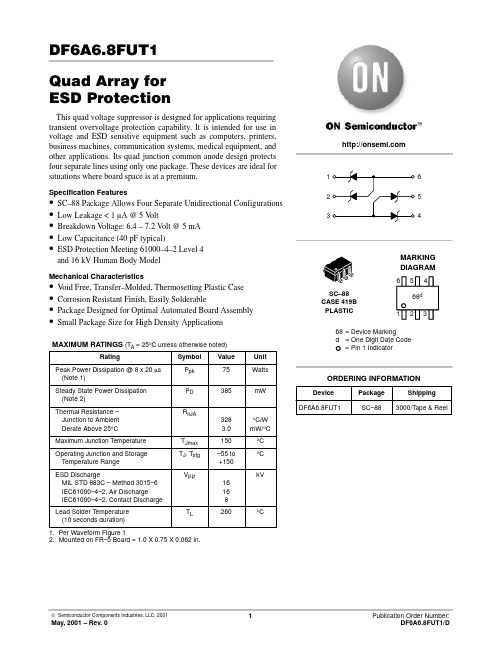
DF6A6.8FUT1Quad Array for ESD ProtectionThis quad voltage suppressor is designed for applications requiring transient overvoltage protection capability. It is intended for use in voltage and ESD sensitive equipment such as computers, printers,business machines, communication systems, medical equipment, and other applications. Its quad junction common anode design protects four separate lines using only one package. These devices are ideal for situations where board space is at a premium.Specification Features•SC–88 Package Allows Four Separate Unidirectional Configurations •Low Leakage < 1 m A @ 5 V olt•Breakdown V oltage: 6.4 – 7.2 V olt @ 5 mA •Low Capacitance (40 pF typical)•ESD Protection Meeting 61000–4–2 Level 4and 16 kV Human Body ModelMechanical Characteristics•V oid Free, Transfer–Molded, Thermosetting Plastic Case •Corrosion Resistant Finish, Easily Solderable•Package Designed for Optimal Automated Board Assembly •Small Package Size for High Density ApplicationsMAXIMUM RATINGS (T= 25°C unless otherwise noted)1.Per Waveform Figure 12.Mounted on FR–5 Board = 1.0 X 0.75 X 0.062 in.6413Device Package Shipping ORDERING INFORMATIONDF6A6.8FUT1SC–883000/T ape & Reel52V–I CurveVELECTRICAL CHARACTERISTICSFigure 1. 8 × 20 m s Pulse Waveform1009080706050403020100020406080t, TIME (m s)% O F P E A K P U L S E C U R R E N TFigure 2. Capacitance454035305025152010135BIAS VOLTAGE (VOLTS)T Y P I C A L C A P A C I T AN C E (p F )421 M H z F R E Q U E N C Y Figure 3. Forward VoltageFigure 4. Clamping Voltage versus PeakPulse CurrentV F , FORWARD VOLTAGE (VOLTS)V C , CLAMPING VOLTAGE (VOLTS)I , F O R W A R D C U R R E N T (A )F 0.010.110.001PACKAGE DIMENSIONSSC–88 (SOT–363)CASE 419B–010.5 mm (min)0.4 m m (m i n )NOTES:1.DIMENSIONING AND TOLERANCING PER ANSI Y14.5M, 1982.2.CONTROLLING DIMENSION: INCH.DIM A MIN MAX MIN MAX MILLIMETERS1.802.200.0710.087INCHES B 1.15 1.350.0450.053C 0.80 1.100.0310.043D 0.100.300.0040.012G 0.65 BSC 0.026 BSC H ---0.10---0.004J 0.100.250.0040.010K 0.100.300.0040.012N 0.20 REF 0.008 REF S 2.00 2.200.0790.087V0.300.400.0120.016ON Semiconductor and are trademarks of Semiconductor Components Industries, LLC (SCILLC). SCILLC reserves the right to make changes without further notice to any products herein. SCILLC makes no warranty, representation or guarantee regarding the suitability of its products for any particular purpose, nor does SCILLC assume any liability arising out of the application or use of any product or circuit, and specifically disclaims any and all liability, including without limitation special, consequential or incidental damages. “Typical” parameters which may be provided in SCILLC data sheets and/or specifications can and do vary in different applications and actual performance may vary over time. All operating parameters, including “Typicals” must be validated for each customer application by customer’s technical experts. SCILLC does not convey any license under its patent rights nor the rights of others.SCILLC products are not designed, intended, or authorized for use as components in systems intended for surgical implant into the body, or other applications intended to support or sustain life, or for any other application in which the failure of the SCILLC product could create a situation where personal injury or death may occur. Should Buyer purchase or use SCILLC products for any such unintended or unauthorized application, Buyer shall indemnify and hold SCILLC and its officers, employees, subsidiaries, affiliates, and distributors harmless against all claims, costs, damages, and expenses, and reasonable attorney fees arising out of, directly or indirectly, any claim of personal injury or death associated with such unintended or unauthorized use, even if such claim alleges that SCILLC was negligent regarding the design or manufacture of the part. SCILLC is an Equal Opportunity/Affirmative Action Employer. PUBLICATION ORDERING INFORMATIONCENTRAL/SOUTH AMERICA:Spanish Phone:303–308–7143 (Mon–Fri 8:00am to 5:00pm MST)Email:ONlit–spanish@Toll–Free from Mexico: Dial 01–800–288–2872 for Access –then Dial 866–297–9322ASIA/PACIFIC: LDC for ON Semiconductor – Asia SupportPhone:1–303–675–2121 (Tue–Fri 9:00am to 1:00pm, Hong Kong Time)Toll Free from Hong Kong & Singapore:001–800–4422–3781Email: ONlit–asia@JAPAN: ON Semiconductor, Japan Customer Focus Center4–32–1 Nishi–Gotanda, Shinagawa–ku, Tokyo, Japan 141–0031Phone: 81–3–5740–2700。
富斯-i6遥控器中文说明书

富斯-i6遥控器中⽂说明书Digital proportional radio control system1. Introduction (2)简介2. Service (2)服务3. Special symbols (3)特殊标志4. Safety guide (3)安全指导5. 2.4GHz System 2.4G (5)系统6.System characteristic s 系统特征 (6)7. Transmitter specifications 发射机参数 (7)8.FS-iA6Receiver FS -iA6接收机..................................................................................................................7-109. FS-IA6B Receiver operation instruction 接收机操作说明.10-16..................................................................................10. O n Off 开机关机17 ........................................................................................................................................11. Definition of key functions 按键定义. (17) 12. Warning 警告 ..............................................................................................................................................1813. ...................................................................................Right and left stick can be adjustable. 左右⼿摇杆模式调整1914. Main screen 开机画⾯ (20)15. Main menu (21)主菜单16. System settings ............................................................................................................................21 系统设置 16.01. Model select .........................................................................................................................模型选择2116.02. Model name 模型名称 (22)Type select 类型选择.........................................................................................................................16.03.22Model copy 模型复制....................................................................................................................... ..16.04.22 Model reset 模型重置16.05. ...................................................................................................................... ...23 16.06. Trainer mode 教练模式......................................................................................................................23 16.07. Student mode ..................................................................................................................... 学员模式23 16.08. Sticks mode 摇杆模式........................................................................................................................ 24 RX setup 接收机设置.....................................................................................................................16.09. 24-2616.10. LCD brightness 显⽰屏亮度 (27)Firmware version 固件版本................................................................................................................16.11. 27Firmware update 固件升级.................................................................................................................16.12. 2717. Functions settings (28)功能设置 17.01.Reverse .................................................................................................................................. 正逆转2817.02. End points .................................................................................................................... 舵机最⼤⾏程2917.03. Display ....................................................................................................................................... 显⽰2917.04. Auxiliary channels ............................................................................................................... 辅助通道2917.05.Sub trim ..................................................................................................................................... 微调3017.06.Dual rate / exponential .............................................................................................. 双重⽐例/指数3017.07.Throttle curve ..................................................................................................................... 油门曲线3017.08. Pitch curve (variable pitch helicopter only).............................. 螺距曲线(仅适⽤于螺距可变直升机)31 17.09. Swash AFR ................................................................................................. .. 直升机螺距混控系统 3117.10. Mix ............................................................................................................................................. 混控31 升降舵(仅适⽤于飞机)17.11.Elevon (airplane only) (32)17.12.V tail (airplane only)..................................................................................... V 型尾翼(仅适⽤于飞机)3217.13.Gyroscope (helicopter only)....................................................................... 陀螺仪(仅适⽤于直升机)3217.14.Switches assign ................................................................................................................. 开关分配 3317.15. Throttle hold ........................................................................................................................ 油门锁定3318. Packaging content 34包装内容.....................................................................................................................19. FCC Statement 声明.. (34)Table of contentsDigital proportional radio control system多⼈⼀起操作的时候间距⾄少要20CM以上。
G680资料
VRESET VRESET
VOH VOL VOH VOL
tRST
Propagation delays not shown for clarity.
Functional Diagram
VDD Low-Voltage Detect
+
LTH R High-Voltage Detect HTH One Shot S Delay Line Q RESET Q RESET
VCC
HTH 1
5
Vcc
VCC HTH RPULL-UP * VCC
GND
2
G680/G681
G680/G681
LTH RESET (RESET) GND
µP
RESET INPUT GND
LTH 3 SOT23-5
() is for G680H
4
RESET(RESET)
*G681 ONLY
Ver: 03 Preliminary
元器件交易网
Global Mixed-mode Technology Inc.
G680/G681
Microprocessor Reset IC
Features
High ±2% Voltage Threshold Accuracy Independently Adjustable High- and Low-
Electrical Characteristics
(VCC = full range, TA = -40°C to +105°C, unless otherwise noted. Typical values are at TA = +25°C, VCC = 3.3V (Note 1) PARAMETER
5806 中文资料(6849)
綠色PWM control IC---SG6848特色支持”Blue Angle”之Green-Mode5μA低啟動电流3mA低操作电流脈衝上升沿遮沒定功率輸出保護内置同步斜率補償最少外部组件低成本解決方案超小型SOT-26 封装应用功率低于20W的通用开关式电源Adapter:打印机, 游戏机, 随身听电池充电器:可攜電子產品电视机、DVD、家电产品中的开关电源概述绿色工作模式PWM控制器SG6848具有许多特殊的功能和完善的保护特性。
因为它是用Bi-CMOS工艺制造的,可大幅度降低了启动和运作时功耗,启动电流仅30μA,工作时仅吸收电流3mA。
SG6848在正常工作时的频率是固定的,但是当输出功率下降到额定值的四分之一时,频率便随着输出功率的减小而下降,从而减少了在负载电流很小或者待机状态时的功耗。
该器件中还采用了同步斜率补偿技术,它可以确保连续模式工作时电流回路的稳定性。
该器件内含电源电压补偿电路,因此输入电压在很宽范围内变化时,开关电源可维持恒定输出功率,该器件还具有过热保护功能。
SG6848内部还具有限功率控制器,因此具有超功率保护功能,从而可实现限制电源功率的安全要求.SG6848用于功率低于20W的通用开关式电源和回扫式转换器,打印机、游戏机、随身听的电源转接器,电池充电器,电视机、DVD、家电产品中的开关电源2. 引脚排列及引脚功能SG6848引脚排列如图1所示。
各引脚的功能如下:SG6848T* DIP括號內為SOT261脚(6) GATE:驱动器输出。
内部推挽输出驱动器的输出脚。
该脚输出信号可驱动外接的功率MOSFET。
2腳VDD:电源输入.起动电流输入脚。
在电源输入和该脚之间应接入一只起动电阻。
在离线式开关变换器中,起动电阻的阻值应为1.5MΩ。
调整起动电阻的阻值,可以改变恒定输出功率限制的电源电压补偿。
3脚ncc.4脚SENSE:电流取样。
外接电流取样电阻两端的压降加到该脚。
Futaba 6EX-2.4G 遥控设备中文说明书(pdf)
Futaba6EX-2.4GHzFutaba 6EX-2.4GHz六通道FASST遥控设备(飞机/直升机通用)使用说明书(C) 版权所有2007技术支持: Futaba公司1M23N12014--------------------------------------------------------------------------------------------------------------------------------- 介绍、服务、注意事项。
3规格和内容、术语表。
46EX-2.4GHz设备介绍、发射机控制介绍。
5设备安装.。
7接收机与舵机连接.。
10镍镉电池充电.。
11LCD和程序控制.。
12T6EX-2.4GHz无线电编程.。
14MODL模型选择功能.。
14MODL模型选择功能、REST 数据复位功能。
14ACRO/HELI固定翼/直升机类型选择功能、TRNR教练功能。
15Model模型名设置。
16REVR舵机反向。
16D/R Dual双重比率和指数设置.。
16D/R Dual双重比率设置.。
16EXPO指数.。
17EPA终点调整.。
17TRIM微调设置.。
18FS安全控制(仅油门通道).。
30(固定翼功能)PMX1程序混控#1、PMX2程序混控#2。
19FLPR襟副翼混控、FLTR襟翼微调。
20V-TL V-尾混控.。
21ELVN升降舵混控。
22(直升机功能)N-TH常规油门曲线、N-PI常规螺距曲线、T-TH怠速油门曲线功能。
24I-PI怠速螺距曲线功能、HOLD油门保持功能。
25REVO螺距-方向舵混控功能、GYRO陀螺仪混控功能。
26SW-T十字盘-油门混控、SWSH十字盘模式选择与十字盘最大舵角调整。
28流程图(固定翼).。
31流程图(直升机).。
32其他T6EX-2.4GHz功能.。
33教练功能、油门关闭功能。
33可调长度的控制杆、改变控制杆模式。
34飞行安全指导.。
1.5KE6.8CA中文资料

1.5KE6.8CA Series1500 Watt Mosorb™ Zener Transient Voltage Suppressors Bidirectional*Mosorb devices are designed to protect voltage sensitive components from high voltage, high–energy transients. They haveexcellent clamping capability, high surge capability, low zener impedance and fast response time. These devices are ON Semiconductor’s exclusive, cost-effective, highly reliable Surmetic axial leaded package and are ideally-suited for use in communication systems, numerical controls, process controls, medical equipment, business machines, power supplies and many other industrial/ consumer applications, to protect CMOS, MOS and Bipolar integrated circuits.Specification Features:•Working Peak Reverse V oltage Range – 5.8 V to 214 V •Peak Power – 1500 Watts @ 1 ms•ESD Rating of Class 3 (>16 KV) per Human Body Model •Maximum Clamp V oltage @ Peak Pulse Current•Low Leakage < 5 µA above 10 V•UL 497B for Isolated Loop Circuit Protection•Response Time is typically < 1 nsMechanical Characteristics:CASE:V oid-free, transfer-molded, thermosetting plasticFINISH:All external surfaces are corrosion resistant and leads are readily solderableMAXIMUM LEAD TEMPERATURE FOR SOLDERING PURPOSES: 230°C, 1/16″ from the case for 10 secondsPOLARITY:Cathode band does not imply polarityMOUNTING POSITION:AnyMAXIMUM RATINGSA Figure 2.*Please see 1N6267A to 1N6306A (1.5KE6.8A – 1.5KE250A)for Unidirectional DevicesDevice Packaging ShippingORDERING INFORMATION1.5KExxCA Axial Lead500 Units/Box 1.5KExxCARL4Axial Lead1500/T ape & ReelELECTRICAL CHARACTERISTICS(T= 25°C unless otherwise noted)ELECTRICAL CHARACTERISTICS (T = 25°C unless otherwise noted.)RWM greater than the dc or continuous peak operating voltage level.2.V BR measured at pulse test current I T at an ambient temperature of 25°C.3.Surge current waveform per Figure 4 and derate per Figures 1 and 2.Figure 1. Pulse Rating Curve1008060402000255075100125150175200P E A K P U L S E D E R A T I N G I N % O F P E A K P O W E R O R C U R R E N T @ T A = 25C T A , AMBIENT TEMPERATURE (_C)Figure 2. Pulse Derating Curve255075100125150175200P D , S T E A D Y S T A T E P O W E R D I S S I P A T I O N (W A T T S )T L , LEAD TEMPERATURE (_C)Figure 3. Steady State Power Derating 0t, TIME (ms)Figure 4. Pulse Waveform1µs 10µs 100µs 1 ms 10 ms100101t P , PULSE WIDTHP P K , P E A K P O W E R (k W )0.1µs_1N6373, ICTE-5, MPTE-5,through1N6389, ICTE-45,C, MPTE-45,C1.5KE6.8CA through 1.5KE200CAFigure 5. Dynamic Impedance10005002001000.30.50.712357102030∆V BR , INSTANTANEOUS INCREASE IN V BRABOVE V BR(NOM) (VOLTS)0.30.50.712357102030∆V BR , INSTANTANEOUS INCREASE IN V BRABOVE V BR(NOM) (VOLTS)I T , T E S T C U R R E N T (A M P S )Figure 6. Typical Derating Factor for Duty CycleD E R A T I N G F A C T O R10.70.50.30.050.10.010.020.030.07D, DUTY CYCLE (%)APPLICATION NOTESRESPONSE TIMEIn most applications, the transient suppressor device is placed in parallel with the equipment or component to be protected. In this situation, there is a time delay associated with the capacitance of the device and an overshoot condition associated with the inductance of the device and the inductance of the connection method. The capacitance effect is of minor importance in the parallel protection scheme because it only produces a time delay in the transition from the operating voltage to the clamp voltage as shown in Figure 7.The inductive effects in the device are due to actual turn-on time (time required for the device to go from zero current to full current) and lead inductance. This inductive effect produces an overshoot in the voltage across the equipment or component being protected as shown in Figure 8. Minimizing this overshoot is very important in the application, since the main purpose for adding a transient suppressor is to clamp voltage spikes. These devices have excellent response time, typically in the picosecond range and negligible inductance. However, external inductive effects could produce unacceptable overshoot. Propercircuit layout, minimum lead lengths and placing the suppressor device as close as possible to the equipment or components to be protected will minimize this overshoot.Some input impedance represented by Z in is essential to prevent overstress of the protection device. This impedance should be as high as possible, without restricting the circuit operation.DUTY CYCLE DERATINGThe data of Figure 1 applies for non-repetitive conditions and at a lead temperature of 25°C. If the duty cycle increases,the peak power must be reduced as indicated by the curves of Figure 6. Average power must be derated as the lead or ambient temperature rises above 25°C. The average power derating curve normally given on data sheets may be normalized and used for this purpose.At first glance the derating curves of Figure 6 appear to be in error as the 10 ms pulse has a higher derating factor than the 10 µs pulse. However, when the derating factor for a given pulse of Figure 6 is multiplied by the peak power value of Figure 1 for the same pulse, the results follow the expected trend.TYPICAL PROTECTION CIRCUITVFigure 7. Figure 8.UL RECOGNITION*The entire series has Underwriters Laboratory Recognition for the classification of protectors (QVGV2) under the UL standard for safety 497B and File #116110. Many competitors only have one or two devices recognized or have recognition in a non-protective category. Some competitors have no recognition at all. With the UL497B recognition, our parts successfully passed several tests including Strike V oltage Breakdown test, Endurance Conditioning, Temperature test, Dielectric V oltage-Withstand test, Discharge test and several more. Whereas, some competitors have only passed a flammability test for the package material, we have been recognized for much more to be included in their Protector category.*Applies to 1.5KE6.8CA – 1.5KE250CACLIPPER BIDIRECTIONAL DEVICES1.Clipper-bidirectional devices are available in the1.5KEXXA series and are designated with a “CA”suffix; for example, 1.5KE18CA. Contact your nearest ON Semiconductor representative.2.Clipper-bidirectional part numbers are tested in bothdirections to electrical parameters in preceeding table (except for V F which does not apply).3.The 1N6267A through 1N6303A series are JEDECregistered devices and the registration does not includea “CA” suffix. To order clipper-bidirectional devicesone must add CA to the 1.5KE device title.OUTLINE DIMENSIONS1500 Watt Mosorb tTransient Voltage Suppressors – Axial LeadedMOSORB CASE 41A–04ISSUE DDIMA MIN MAX MIN MAX MILLIMETERS0.3350.3748.509.50INCHES B 0.1890.209 4.80 5.30D 0.0380.0420.96 1.06K 1.000---25.40---P---0.050--- 1.27NOTES:1.DIMENSIONING AND TOLERANCING PER ANSI Y14.5M, 1982.2.CONTROLLING DIMENSION: INCH.3.LEAD FINISH AND DIAMETER UNCONTROLLED IN DIMENSION P.4.041A-01 THRU 041A-03 OBSOLETE, NEW STANDARD 041A-04.Mosorb is a trademark of Semiconductor Components Industries, LLC.ON Semiconductor and are trademarks of Semiconductor Components Industries, LLC (SCILLC). SCILLC reserves the right to make changes without further notice to any products herein. SCILLC makes no warranty, representation or guarantee regarding the suitability of its products for any particular purpose, nor does SCILLC assume any liability arising out of the application or use of any product or circuit, and specifically disclaims any and all liability, including without limitation special, consequential or incidental damages. “Typical” parameters which may be provided in SCILLC data sheets and/or specifications can and do vary in different applications and actual performance may vary over time. All operating parameters, including “Typicals” must be validated for each customer application by customer’s technical experts. SCILLC does not convey any license under its patent rights nor the rights of others.SCILLC products are not designed, intended, or authorized for use as components in systems intended for surgical implant into the body, or other applications intended to support or sustain life, or for any other application in which the failure of the SCILLC product could create a situation where personal injury or death may occur. Should Buyer purchase or use SCILLC products for any such unintended or unauthorized application, Buyer shall indemnify and hold SCILLC and its officers, employees, subsidiaries, affiliates, and distributors harmless against all claims, costs, damages, and expenses, and reasonable attorney fees arising out of, directly or indirectly, any claim of personal injury or death associated with such unintended or unauthorized use, even if such claim alleges that SCILLC was negligent regarding the design or manufacture of the part. SCILLC is an Equal Opportunity/Affirmative Action Employer. PUBLICATION ORDERING INFORMATIONJAPAN: ON Semiconductor, Japan Customer Focus Center4–32–1 Nishi–Gotanda, Shinagawa–ku, Tokyo, Japan 141–0031Phone: 81–3–5740–2700Email: r14525@。
AD8648中文资料
FEATURES
Low offset voltage: 2.5 mV max Single-supply operation: 2.7 V to 5.5 V Low noise: 6 nV/√Hz Wide bandwidth: 24 MHz Slew rate: 12 V/μs High output current: 150 mA No phase reversal Low input bias current: 1 pA Low supply current: 2 mA max Unity-gain stable
APPLICATIONS
Barcode scanners Battery-powered instrumentation Multipole filters Sensors ASIC input or output amplifiers Audio Photodiode amplification
GENERAL DESCRIPTION
Min Typ Max Unit
0.7 2.5 mV
3.2 mV
2.0 7.5 μV/°C
0.2 1
pA
50 pA
550 pA
0.1 0.5 pA
Symbol Conditions
VOS
ΔVOS/ΔT IB
IOS
VCM CMRR AVO CDIFF CCM
VCM = 0 V to 5 V −40°C < TA < +125°C −40°C < TA < +125°C
−40°C < TA < +85°C −40°C < TA < +125°C
FUT1基因对大长杂交母猪产仔数的影响
13 DNA提 取 采 用苯 酚 一氯 仿一 异 戊 醇抽 提方 法 提 取 .
> .5 。 00 )
关键 词 :
1 因 ; 殖性 能 ; 长 杂交 母 猪 基 繁 大
文献 标 识 码 : A 文 章顺 序 编 号 : 6 2 5 9 2 1 1 — 1 1 叭 1 7 — 1 0( 0 0) 0 0 1 一
中 图分 类 号 :8 82 ¥ 2 .
Efe t f f c o F lGe eo te ieo wswih Hy rd z to t e r h r n n r c n n Lit rS z f So t b i i a i n bewe n Yo ks iea d La d a e
随 着 分 子 生 物 学 在 动 物 遗 传 育 种 中 的 应 用 .对 数 量 性 状 主 效 基 因 的 研 究 成 为 必 然 。产 仔 数 是 猪 最 为 重 要 的 经 济
T q聚 合酶 、 h 等 购 自石 河子 超科 生 物器 材 公 司 。引 a H aI酶
物 根 据 , 上 海 生 工 生 物 有 限 公 CI C G C G G T C r A G一 反 向 U正 5一 A C A G C C T r A 3 : T
( . 石 河 子 市畜 牧兽 医工 作站 , 疆 1 新疆 新 石河 子 8 2 0 ;. 3 0 0 2石河 子 大学 动 物科 技 学 院 , 疆 新 石河 子 820 ) 3 00
摘要 : 用 P R R L 利 C — F P技 术 检 测 了 18头 大 长 杂 交 母 猪 刚 基 因 多 态性 , 析 了 l 1 分 1基 因 与 产 仔 数 的 关 系。 1 基 因A 、 G、 G 基 因 型 频 率 分 别 为 O1 , - ,.2 G .103 05 。刚 7 1三 种 基 因 型 母 猪 在 总 产 仔 数 和 产 活 仔 数 方 面 都 无 显 著 差 异 ( P
8ETX06中文资料
T J = 25˚C 1
100
Junction Capacitance - C T (pF)
0.1 0 0.5 1 1.5 2 2.5 3 3.5 4 4.5 Forward Voltage Drop - VFM (V)
Fig. 1 - Typical Forward Voltage Drop Characteristics
2 4.3 70
12 10
Units
°C
°C/W
g (oz) Kg-cm lbf.in
Typical Socket Mount Mounting Surface, Flat, Smooth and Greased
2
元器件交易网
Instantaneous Forward Current - I F (A)
Fig. 6 - Max. Allowable Case Temperature Vs. Average Forward Current
160
140
DC
120
100
Square wave (D = 0.50)
80 Rated Vr applied
60
see note (3)
40 0 2 4 6 8 10 12 Average Forward Current - IF(AV)(A) Fig. 7 - Max. Allowable Case Temperature
Parameters
Min Typ Max Units Test Conditions
trr
Reverse Recovery Time
IRRM
Peak Recovery Current
Qrr
Reverse Recovery Charge
TD62081APG中文资料

Unit V
mA/ch V mA V mA
W
°C °C
2
2006-06-13
元器件交易网
Recommended Operating Conditions (Ta = −40 to 85°C)
Characteristics
Symbol
Type TD62081APG/AFG TD62082APG/AFG TD62083APG/AFG TD62084APG/AFG
Input Base Resistor External
10.5-kΩ + 7 V Zenner diode
2.7 kΩ
10.5 kΩ
Designation
General purpose 14 V to 25 V PMOS
Features
Output current (single output) 500 mA (max) (TD62081APG/AFG series) High sustaining voltage output 50 V (min) (TD62081APG/AFG series) Output clamp diodes Inputs compatible with various types of logic. Package type-APG: DIP-18 pin Package type-AFG: SOP-18 pin
IIN (OFF)
Open
7. VF
VF Open
5. VIN (ON)
IOUT VIN (ON)
IF
Open VCE
6. IR
IOUT
Open
Open
6A8-T中文资料
DS28009 Rev. 7 - 2
2 of 3
6A05 - 6A10
元器件交易网
Ordering Information
Device 6A05-T 6A1-T 6A2-T 6A4-T 6A6-T 6A8-T 6A10-T
Notes:
(Note 2) Packaging R-6 R-6 R-6 R-6 R-6 R-6 R-6 Shipping 500/Tape & Reel, 13-inch 500/Tape & Reel, 13-inch 500/Tape & Reel, 13-inch 500/Tape & Reel, 13-inch 500/Tape & Reel, 13-inch 500/Tape & Reel, 13-inch 500/Tape & Reel, 13-inch
DS28009 Rev. 7 - 2
1 of 3
6A05 - 6A10
ã Diodes Incorporated
元器件交易网
AVERAGE RECTIFIED CURRENT (A)
6 5 4 3 2 1
B A
Recommended Method (See Derating "A")
INSTANTANEOUS FORWARD VOLTAGE (V) Typical Forward Characteristics
25
THERMAL RESISTANCE JUNCTION TO AMBIENT RqJA - °C/WATT
20
15
10
5
0 0 5 10 15 20 25
LEAD LENGTH TO HEAT SINK (mm) Typical Thermal Resistance (Using Standard Mounting Method "B")
本松材料选型

PA6,玻纤/矿粉35%,阻燃 PA6,玻纤/矿粉35%,阻燃 PA6,玻纤/矿粉35%,阻燃 PA6,玻纤/矿粉35%,阻燃 PA66,玻纤20%,阻燃 PA66,玻纤25%,阻燃 PA66,玻纤30%,阻燃 PA66,玻纤30%,阻燃 PA66,玻纤30%,阻燃 PA66,玻纤30%,阻燃 PA66,玻纤30%,阻燃 PA66,玻纤35%,阻燃 PA66,玻纤35%,阻燃 PA66,玻纤35%,阻燃 PA66,玻纤40%,阻燃 PA66,玻纤40%,阻燃 PA66,玻纤40%,阻燃 PA66,玻纤45%,阻燃 PA66,玻纤50%,阻燃
PA6
A190M6 TD
PA6-MD30 FR
PA6,矿粉30%,阻燃
PA66 PA66 PA66 PA66 PA66 PA66
A280G5 R A280G5 RT A280G6 N A280G6 A A280G7 N A280G9 H
PA66-GF25 PA66-GF25 PA66-GF30 PA66-GF30 PA66-GF35 PA66-GF45 HTN-GF45 HTN-GF45 HTN-GF45 HTN-GF45 PPA-GF30 PPA-GF40 PPA-GF45 PPA-GF35 FR PPA-GF35 FR
PA6-(GF+MD)35 FR PA6-(GF+MD)35 FR PA6-(GF+MD)35 FR PA6-(GF+MD)35 FR PA66-GF20 FR PA66-GF25 FR PA66-GF30 FR PA66-GF30 FR PA66-GF30 FR PA66-GF30 FR PA66-GF30 FR PA66-GF35 FR PA66-GF35 FR PA66-GF35 FR PA66-GF40 FR PA66-GF40 FR PA66-GF40 FR PA66-GF45 FR PA66-GF50 FR
FAR-G6CH-1G8425-L222-R中文资料
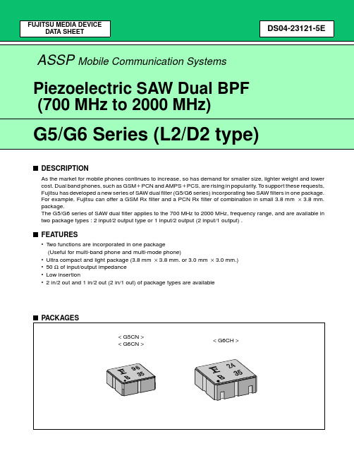
s PACKAGES
< G5CN > < G6CN > < G6CH >
元器件交易网
G5/G6 Series
s PIN ASSIGNMENTS
< BOTTOM VIEW > G5CN package G6CN package
1 2 3 1
G6CH package
2 3
8
2
元器件交易网
G5/G6 Series
s INTERNAL BLOCK DIAGRAM
1 in/2 out type 2 in/2 out type
1
BPF1
7
1
BPF1
7
BPF2
5
3
BPF2Βιβλιοθήκη 51−7 : Pin number
3
元器件交易网
4
8
4
7
6
5 7 6 5
s PIN DESCRIPTIONS
• 1 in/2 out type Pin Pin name 1 2 3 4 5 6 7 8 IN GND GND GND OUT GND OUT GND Description Input Pin (Common) Ground Pin Ground Pin Ground Pin Filter 2 Output Pin Ground Pin Filter 1 Output Pin Ground Pin
s FEATURES
• Two functions are incorporated in one package (Useful for multi-band phone and multi-mode phone) • Ultra compact and light package (3.8 mm × 3.8 mm. or 3.0 mm × 3.0 mm.) • 50 Ω of input/output impedance • Low insertion • 2 in/2 out and 1 in/2 out (2 in/1 out) of package types are available
futaba cgy750中文版说明书

介绍Futaba CGY750是一个组合的3轴陀螺仪,在一个盒子里装上了AVCS陀螺和磁头调速器。
它的尖端MEMS(微电子机械系统)传感器设计,超高速处理速度和先进的PID控制算法使其在尺寸、重量和性能方面领先于其他所有的陀螺仪。
CGY750已经被优化为无人直升机的工作。
保修和服务(美国)如果在设置或操作你的CGY750时候遇到任何的困难,请先查阅说明书,其次你也可以和你的经销商联系或者联系futaba的服务中心,传真和电话如下:或fax(217)-398-7721,tel (217)398-0007如果你无法解决这个问题,请将这个系统放置在它的原包装中,并附上一张纸条,对这些问题进行详细的描述。
在你的纸条上包括以下的内容:症状(包括出现的问题)系统(发射器、接收机、伺服器和模型号)模型(模型的名称)模型编号和数量你的名字,地址和电话号码将各自的问题发送到futaba授权服务中心双叶服务中心阿波罗1号3002号伊利诺伊州61822特征三轴陀螺和调速器在一个盒子里高速运转操作和极小的延迟具有更大的稳定性低姿态、小尺寸和轻重量陀螺仪和控制器的尺寸为44x29x12mm,13g使用128X36点的黑白OLED屏(有光显示),即使在阳光直射下仍有高亮度和对比度。
设置分为基础和专业的菜单,这基础的菜单是为初始设置,专业的菜单是为更多高级的设置。
当使用CIU-2接口时,固件可以从windows系统上跟新。
SBUS是兼容的,只需要一个的在这个总线接收机和CGY750控制盒之间为了操作陀螺部分采用先进的和自适应的PID控制回路小和低姿态三轴陀螺仪,21x21x8.5mm,8g舵(偏航)部分能够感应到角的速度,升到+/-1200度/秒。
兼容1520的模拟(70Hz),1520数字(280Hz)和760数字(560Hz)的尾转子伺服系统。
3D和飞行运动模式前馈选项允许CGY750可以在操作期间进行其它的操作,这就导致了更精确的修正和精确的操作。
DF8A6.2FK资料
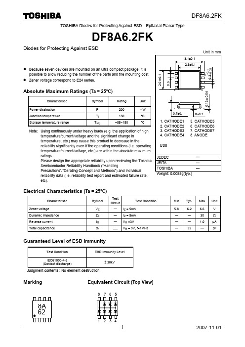
TOSHIBA Diodes for Protecting Against ESD Epitaxial Planar TypeDF8A6.2FKDiodes for Protecting Against ESDz Because seven devices are mounted on an ultra compact package, it ispossible to allow reducing the number of the parts and the mounting cost. z Zener voltage correspond to E24 series.Absolute Maximum Ratings (Ta = 25°C)Characteristic Symbol Rating UnitPower dissipation P 200mWJunction temperature T j 150 °CStorage temperature rangeT stg−55~150 °C Note: Using continuously under heavy loads (e.g. the application of hightemperature/current/voltage and the significant change in temperature, etc.) may cause this product to decrease in thereliability significantly even if the operating conditions (i.e. operating temperature/current/voltage, etc.) are within the absolute maximum ratings.Please design the appropriate reliability upon reviewing the Toshiba Semiconductor Reliability Handbook (“HandlingPrecautions”/“Derating Concept and Methods”) and individual reliability data (i.e. reliability test report and estimated failure rate, etc).Electrical Characteristics (Ta = 25°C)Characteristic SymbolTestCircuitTest ConditionMin Typ. Max Unit Zener voltage V Z ― I Z = 5mA 5.8 6.26.6VDynamic impedance Z Z ― I Z = 5mA ― ― 30 Ω Reverse current I R ―V R =3V― ― 1.0 μA Total capacitanceC T―V R = 0V, f=1MHz―55⎯ pFGuaranteed Level of ESD ImmunityTest Condition ESD Immunity LevelIEC61000-4-2(Contact discharge)± 30kVJudgment contents : No element destructionMarkingEquivalent Circuit (Top View)RESTRICTIONS ON PRODUCT USE20070701-EN GENERAL •The information contained herein is subject to change without notice.•TOSHIBA is continually working to improve the quality and reliability of its products. Nevertheless, semiconductor devices in general can malfunction or fail due to their inherent electrical sensitivity and vulnerability to physical stress. It is the responsibility of the buyer, when utilizing TOSHIBA products, to comply with the standards of safety in making a safe design for the entire system, and to avoid situations in which a malfunction or failure of such TOSHIBA products could cause loss of human life, bodily injury or damage to property.In developing your designs, please ensure that TOSHIBA products are used within specified operating ranges as set forth in the most recent TOSHIBA products specifications. Also, please keep in mind the precautions and conditions set forth in the “Handling Guide for Semiconductor Devices,” or “TOSHIBA Semiconductor Reliability Handbook” etc.• The TOSHIBA products listed in this document are intended for usage in general electronics applications (computer, personal equipment, office equipment, measuring equipment, industrial robotics, domestic appliances, etc.).These TOSHIBA products are neither intended nor warranted for usage in equipment that requires extraordinarily high quality and/or reliability or a malfunction or failure of which may cause loss of human life or bodily injury (“Unintended Usage”). Unintended Usage include atomic energy control instruments, airplane or spaceship instruments, transportation instruments, traffic signal instruments, combustion control instruments, medical instruments, all types of safety devices, etc.. Unintended Usage of TOSHIBA products listed in his document shall be made at the customer’s own risk.•The products described in this document shall not be used or embedded to any downstream products of which manufacture, use and/or sale are prohibited under any applicable laws and regulations.• The information contained herein is presented only as a guide for the applications of our products. No responsibility is assumed by TOSHIBA for any infringements of patents or other rights of the third parties which may result from its use. No license is granted by implication or otherwise under any patents or other rights of TOSHIBA or the third parties.• Please contact your sales representative for product-by-product details in this document regarding RoHS compatibility. Please use these products in this document in compliance with all applicable laws and regulations that regulate the inclusion or use of controlled substances. Toshiba assumes no liability for damage or losses occurring as a result of noncompliance with applicable laws and regulations.。
Futaba T6J简明中文说明书
Futaba T6J 中文手册本手册由Kyle翻译制作,Email:****************因水平有限,文中可能存在错误,如果您发现翻译不当的地方请发Email或通过QQ告诉我,谢谢!更改油门摇杆顺滑度程序设置更改摇杆长度更改摇杆模式(改手)6J-2.4GHZ系统说明重要说明!任何时候都要先开发射机,然后再开接收机,关机时先关接收机,再关发射机。
在发射机没有打开的情况下,接收机无法开启。
更改油门摇杆顺滑度遥控器提供两种油门顺滑度,通过更换两个金属薄片来实现。
控买来的时候默认装的是直板式的“直升机油门阻尼调节片”,下图则是附带提供的“固定翼油门阻尼调节片”。
打开遥控器电池盖,拔下左边的插头,然后拆下整个后盖,看到右边那个金属薄片,可根据自己的喜好决定是否更换“阻尼调节片”。
拉距测试1)按住MODE键开机,屏幕会显示POWR DOWN,表示进入“低功率拉距测试模式”,这时候发射机会降低无线信号发射功率,并会每隔3秒发出一次“哔”声,正常情况在该模式下,离开飞机30-50步的距离不会失控,否则请检查发射机电池或飞机各组件,直到故障排除再起飞。
2)“低功率拉距测试模式”会在90秒后发出两声连续的“哔”声,然后自动恢复为正常模式。
3)任何时候都不要在“低功率拉距测试模式”下飞行。
接收机连线报警和警告T6J提供几种不同的警告和报警声。
举例说,不管是固定翼或直升机模式,当电池电压下降到推荐的最低电压时会发出报警声。
在直升机模式下,会有一些额外的警告/报警声:摇杆位置,油门锁定,idle up被激活。
这些内置的安全特性可确保你的模型安全与模型爱好的乐趣。
发射机电池电压T6J发射机提供可编程的低电压报警,当发射机电压低于预设的电池电压时能警告操作者。
当飞行时听到此报警声,请尽快安全降落以避免各种可能的困境。
设置发射机电池电压报警1)同时按住MODE和END键,然后开机。
2)按-/+选择报警电压值。
如果使用4节AA碱性(干电池),请将报警电压设置为4.2V。
免疫球蛋白A肾病患者血清FUT8水平与肾小管间质损伤相关性分析
免疫球蛋白A肾病患者血清FUT8水平与肾小管间质损伤相关性分析姜欣佐;宋国良;田雪山【期刊名称】《国际检验医学杂志》【年(卷),期】2024(45)7【摘要】目的探讨免疫球蛋白A肾病(IgAN)患者血清α1-6-岩藻糖基转移酶(FUT8)水平与肾小管间质损伤的关系。
方法选取2020年3月至2022年12月佳木斯大学宏大医院收治的89例IgAN患者作为IgAN组和63例性别和年龄匹配的健康志愿者作为对照组。
根据小管萎缩及间质纤维化(T)分级将IgAN组患者分为T0组(28例)、T1组(39例)、T2组(22例),根据间质性炎症指数(Inf I)将患者分为轻度组(0~1分,30例)、中度组(2~3分,42例)、重度组(4分,17例)。
检测各组血清FUT8水平,并分析血清FUT8水平与IgAN临床参数、T分级、Inf I的相关性。
结果IgAN组收缩压、血肌酐、尿素氮、FUT8水平高于对照组(P<0.05),血清白蛋白和估算肾小球滤过率(eGFR)低于对照组(P<0.05)。
不同T分级、间质性炎症细胞浸润程度IgAN患者血清FUT8水平比较差异有统计学意义(P<0.05),T2组血清FUT8水平高于T1组和T0组(P<0.05),重度组血清FUT8水平高于中度组、轻度组(P<0.05)。
IgAN患者血清FUT8水平与血肌酐、T分级、Inf I呈正相关(P<0.05),与eGFR呈负相关(P<0.05)。
结论IgAN患者血清FUT8水平升高,且与肾小管间质损伤加重、肾功能下降有关。
【总页数】5页(P809-812)【作者】姜欣佐;宋国良;田雪山【作者单位】佳木斯大学宏大医院检验科;佳木斯中心医院检验科【正文语种】中文【中图分类】R446.6;R692【相关文献】1.慢性肾脏病合并急性肾小管间质损伤患者血清NGAL和尿KIM-1水平变化及临床意义2.IgA肾病肾组织诱骗受体2表达变化与肾小管、间质损伤的相关性分析3.血清三项指标的表达水平与原发性肾病综合征肾小管间质纤维化的相关性研究4.尿白介素-6水平与IgA肾病肾小管间质损伤的相关性研究5.IgA肾病患者血清sIL-2R的测定与肾小管间质病变临床病理相关性分析因版权原因,仅展示原文概要,查看原文内容请购买。
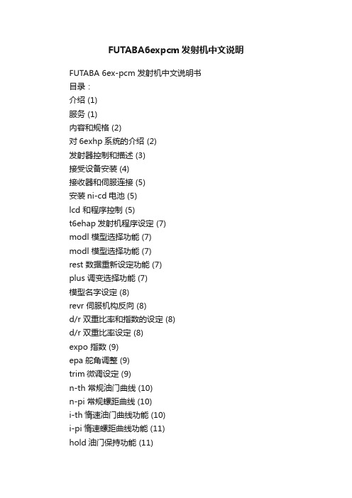
FUTABA6expcm发射机中文说明
FUTABA6expcm发射机中文说明FUTABA 6ex-pcm 发射机中文说明书目录:介绍 (1)服务 (1)内容和规格 (2)对6exhp系统的介绍 (2)发射器控制和描述 (3)接受设备安装 (4)接收器和伺服连接 (5)安装ni-cd电池 (5)lcd 和程序控制 (5)t6ehap发射机程序设定 (7)modl 模型选择功能 (7)modl 模型选择功能 (7)rest 数据重新设定功能 (7)plus 调变选择功能 (7)模型名字设定 (8)revr 伺服机构反向 (8)d/r 双重比率和指数的设定 (8)d/r 双重比率设定 (8)expo 指数 (9)epa 舵角调整 (9)trim微调设定 (9)n-th 常规油门曲线 (10)n-pi 常规螺距曲线 (10)i-th惰速油门曲线功能 (10)i-pi惰速螺距曲线功能 (11)hold油门保持功能 (11)revo 螺距-方向舵混控功能 (12)gyro 陀螺仪 (12)swsh 十字盘模式选择和舵角调整(swash afr) (13)fs 安全控制(仅pcm模式下有效) (14)流程图 (15)t6exhp 的其他功能 (16)教练功能 (16)可调长度的操纵杆 (16)改变手柄模式 (16)飞行安全指导方针 (17)飞行准备 (17)模型数据记录页 (19)介绍非常感谢你购买futaba 6exhp数字比例r/c直升飞机控制系统。
如果这是你的第一台“微电脑”遥控设备,并且是你用于直升飞机领域的初级装备,这台设备会比"非微电脑"遥控设备更精确和更容易使用。
虽然这是智能的飞行遥控系统,但为了使你的futaba 6exhp设备更好地被好使用和安全地操作它,你一定要仔细地阅读以下所有说明。
提议: 如果,当你读指令的时候,你对一些程序或功能是不是很了解的时候,或者显示“stuck”的时候,请查阅本说明书。
通常,有些功能或程序在另外的环境中才会被使用。
- 1、下载文档前请自行甄别文档内容的完整性,平台不提供额外的编辑、内容补充、找答案等附加服务。
- 2、"仅部分预览"的文档,不可在线预览部分如存在完整性等问题,可反馈申请退款(可完整预览的文档不适用该条件!)。
- 3、如文档侵犯您的权益,请联系客服反馈,我们会尽快为您处理(人工客服工作时间:9:00-18:30)。
DF6A6.8FUT1Quad Array forESD ProtectionThis quad voltage suppressor is designed for applications requiring transient overvoltage protection capability. It is intended for use in voltage and ESD sensitive equipment such as computers, printers, business machines, communication systems, medical equipment, and other applications. Its quad junction common anode design protects four separate lines using only one package. These devices are ideal for situations where board space is at a premium.Specification Features•SC−88 Package Allows Four Separate Unidirectional Configurations •Low Leakage < 1 m A @ 5 V olt•Breakdown V oltage: 6.4 − 7.2 V olt @ 5 mA•Low Capacitance (40 pF typical)•ESD Protection Meeting 61000−4−2 Level 4and 16 kV Human Body Model•Pb−Free Package is AvailableMechanical Characteristics•V oid Free, Transfer−Molded, Thermosetting Plastic Case •Corrosion Resistant Finish, Easily Solderable•Package Designed for Optimal Automated Board Assembly •Small Package Size for High Density ApplicationsMAXIMUM RATINGS (T A = 25°C unless otherwise noted)Rating Symbol Value Unit Peak Power Dissipation @ 8 x 20 m s(Note 1)P pk75WattsSteady State Power Dissipation(Note 2)P D385mWThermal Resistance −Junction−to−Ambient Derate Above 25°C R q JA3283.0°C/WmW/°CMaximum Junction T emperature TJmax150°COperating Junction and Storage Temperature Range T J, T stg−55 to+150°CESD DischargeMIL STD 883C − Method 3015−6 IEC61000−4−2, Air DischargeIEC61000−4−2, Contact Discharge V PP16168kVLead Solder Temperature(10 seconds duration)T L260°CMaximum ratings are those values beyond which device damage can occur. Maximum ratings applied to the device are individual stress limit values (not normal operating conditions) and are not valid simultaneously. If these limits are exceeded, device functional operation is not implied, damage may occur and reliability may be affected.1.Per Waveform Figure 12.Mounted on FR−5 Board = 1.0 X 0.75 X 0.062 in.6413Device Package Shipping†ORDERING INFORMATIONDF6A6.8FUT1SC−88(Pb−Free)3000/T ape & Reel52DF6A6.8FUT1G3000/T ape & ReelSC−88†For information on tape and reel specifications, including part orientation and tape sizes, please refer to our T ape and Reel Packaging Specifications Brochure, BRD8011/D.V−I CurveVELECTRICAL CHARACTERISTICSDevice Device Marking Breakdown Voltage V BR @ 5 mA (Volts)Leakage Current I RM @ V RWM = 5 VTypical Capacitance @ 0 V BiasMaxV F @ I F = 10 mAMax Z Z @5 mA Max Z ZK @0.5 mA Min Nom Max (m A)(pF)(V)(W )(W )DF6A6.8FUT1686.46.87.21.0401.2530300Figure 1. 8 × 20 m s Pulse Waveform1009080706050403020100t, TIME (m s)% O F P E A K P U L S E C U R R E N TFigure 2. Capacitance454035305025152010135BIAS VOLTAGE (VOLTS)T Y P I C A L C A P A C I T A NC E (p F )421 M H z F R E Q U E N C Y Figure 3. Forward VoltageFigure 4. Clamping Voltage versus PeakPulse CurrentV F , FORWARD VOLTAGE (VOLTS)V C , CLAMPING VOLTAGE (VOLTS)I , F O R W A R D C U R R E N T (A )F 0.010.110.001PACKAGE DIMENSIONSSC−88/SC70−6/SOT−363CASE 419B−02NOTES:1.DIMENSIONING AND TOLERANCING PER ANSI Y14.5M, 1982.2.CONTROLLING DIMENSION: INCH.3.419B−01 OBSOLETE, NEW STANDARD 419B−02.DIM MIN NOM MAX MILLIMETERS A 0.800.95 1.10A10.000.050.10A3b 0.100.210.30C 0.100.140.25D 1.80 2.00 2.200.0310.0370.0430.0000.0020.0040.0040.0080.0120.0040.0050.0100.0700.0780.086MIN NOMMAX INCHES0.20 REF 0.008 REFH EE 1.15 1.25 1.35e 0.65 BSC L 0.100.200.302.00 2.10 2.200.0450.0490.0530.026 BSC0.0040.0080.0120.0780.0820.086*For additional information on our Pb−Free strategy and solderingdetails, please download the ON Semiconductor Soldering and Mounting Techniques Reference Manual, SOLDERRM/D.SOLDERING FOOTPRINT*SC−88/SC70−6/SOT−363ON Semiconductor and are registered trademarks of Semiconductor Components Industries, LLC (SCILLC). SCILLC reserves the right to make changes without further notice to any products herein. SCILLC makes no warranty, representation or guarantee regarding the suitability of its products for any particular purpose, nor does SCILLC assume any liability arising out of the application or use of any product or circuit, and specifically disclaims any and all liability, including without limitation special, consequential or incidental damages.“Typical” parameters which may be provided in SCILLC data sheets and/or specifications can and do vary in different applications and actual performance may vary over time. All operating parameters, including “Typicals” must be validated for each customer application by customer’s technical experts. SCILLC does not convey any license under its patent rights nor the rights of others. SCILLC products are not designed, intended, or authorized for use as components in systems intended for surgical implant into the body, or other applications intended to support or sustain life, or for any other application in which the failure of the SCILLC product could create a situation where personal injury or death may occur. Should Buyer purchase or use SCILLC products for any such unintended or unauthorized application, Buyer shall indemnify and hold SCILLC and its officers, employees, subsidiaries, affiliates, and distributors harmless against all claims, costs, damages, and expenses, and reasonable attorney fees arising out of, directly or indirectly, any claim of personal injury or death associated with such unintended or unauthorized use, even if such claim alleges that SCILLC was negligent regarding the design or manufacture of the part. SCILLC is an Equal Opportunity/Affirmative Action Employer. This literature is subject to all applicable copyright laws and is not for resale in any manner.PUBLICATION ORDERING INFORMATION。