XCF32PVO48C中文资料
FPGA可编程逻辑器件芯片XC7A100T-2FGG484C中文规格书
IntroductionArtix®-7 FPGAs are available in -3, -2, -1, -1LI, and -2L speed grades, with -3 having the highest performance. The Artix-7FPGAs predominantly operate at a 1.0V core voltage. The -1LI and -2L devices are screened for lower maximum static power and can operate at lower core voltages for lower dynamic power than the -1 and -2 devices, respectively. The -1LI devices operate only atV CCINT=V CCBRAM=0.95V and have the same speed specifications as the -1 speed grade. The -2L devices can operate at either of two V CCINT voltages, 0.9V and 1.0V and are screened for lower maximum static power. When operated at V CCINT=1.0V, the speed specification of a -2L device is the same as the -2 speed grade. When operated at V CCINT=0.9V, the -2L static and dynamic power is reduced. Artix-7 FPGA DC and AC characteristics are specified in commercial, extended, industrial, expanded (-1Q), and military (-1M) temperature ranges. Except the operating temperature range or unless otherwise noted, all the DC and AC electrical parameters are the same for a particular speed grade (that is, the timing characteristics of a -1M speed grade military device are the same as for a -1C speed grade commercial device). However, only selected speed grades and/or devices are available in each temperature range. For example, -1M is only available in the defense-grade Artix-7Q family and -1Q is only available in XA Artix-7FPGAs.All supply voltage and junction temperature specifications are representative of worst-case conditions. The parameters included are common to popular designs and typical applications.Available device and package combinations can be found in:•7Series FPGAs Overview (DS180)•Defense-Grade 7Series FPGAs Overview (DS185)•XA Artix-7 FPGAs Overview (DS197)DC CharacteristicsArtix-7 FPGAs Data Sheet: DC and AC Switching CharacteristicsDS181 (v1.25) June 18, 2018Product SpecificationTable 1:Absolute Maximum Ratings(1)Symbol Description Min Max Units FPGA LogicV CCINT Internal supply voltage–0.5 1.1VV CCAUX Auxiliary supply voltage–0.5 2.0VV CCBRAM Supply voltage for the block RAM memories–0.5 1.1VV CCO Output drivers supply voltage for HR I/O banks–0.5 3.6VV REF Input reference voltage–0.5 2.0VV IN(2)(3)(4)I/O input voltage–0.4V CCO+0.55V I/O input voltage (when V CCO=3.3V) for V REF and differential I/O standardsexcept TMDS_33(5)–0.4 2.625VV CCBATT Key memory battery backup supply–0.5 2.0V GTP TransceiverV MGTAVCC Analog supply voltage for the GTP transmitter and receiver circuits–0.5 1.1V V MGTAVTT Analog supply voltage for the GTP transmitter and receiver termination circuits–0.5 1.32V V MGTREFCLK Reference clock absolute input voltage–0.5 1.32V V IN Receiver (RXP/RXN) and Transmitter (TXP/TXN) absolute input voltage–0.5 1.26VVersion In:Typical V CCINTDeviceISE 14.7Vivado 2018.2(Table2)N/A 1.22 1.0V XC7A12T, XC7A15T, XC7A25T, XC7A35T, XC7A50T, XC7A75TN/A 1.220.95V XC7A12T, XC7A15T, XC7A25T, XC7A35T, XC7A50T, XC7A75T, XC7A100T,XC7A200TN/A 1.140.9V XC7A12T, XC7A15T, XC7A25T, XC7A35T, XC7A50T, XC7A75T1.10 1.22 1.0V XC7A100T, XC7A200T1.07 1.140.9V XC7A100T, XC7A200TN/A 1.15 1.0V XA7A12T, XA7A15T, XA725T, XA7A35T, XA7A50T, XA7A75T1.07 1.15 1.0V XA7A100T1.06 1.11 1.0V XQ7A100T, XQ7A200TN/A 1.11 1.0V XQ7A50TDeviceSpeed Grade1.0V0.95V0.9V -3-2-2LE-1-1Q-1M-1LI-2LEXC7A12T Vivado tools2018.2 v1.22Vivado tools 2017.4 v1.20N/A N/A Vivado tools2017.4 v1.20Vivado tools2018.1 v1.14XC7A15T Vivado tools 2014.4 v1.14N/A N/A Vivado tools2014.4 v1.14Vivado tools 2014.4 v1.10XC7A25T Vivado tools2018.2 v1.22Vivado tools 2017.4 v1.20N/A N/A Vivado tools2017.4 v1.20Vivado tools2018.1 v1.14XC7A35T Vivado tools 2013.4 v1.11N/A N/A Vivado tools2014.4 v1.14Vivado tools 2013.4 v1.08Selecting the Correct Speed Grade and Voltage in the Vivado ToolsIt is important to select the correct device speed grade and voltage in the Vivado tools for the device that you are selecting.To select the 1.0V speed specifications in the Vivado tools, select the Artix-7, XA Artix-7, or Defense Grade Artix-7Q sub-family, and then select the part name that is the device name followed by the package name followed by the speed grade. For example, select the xc7a100tfgg676-3 part name for the XC7A100T device in the FGG676 package and -3 (1.0V) speed grade or select the xc7a100tfgg676-2L part name for the XC7A100T device in the FGG676 package and -2LE (1.0V) speed grade.To select the -1LI (0.95V) speed specifications in the Vivado tools, select the Artix-7 sub-family and then select the part name that is the device name followed by an “i” followed by the package name followed by the speed grade. For example, select the xc7a100tifgg676-1L part name for the XC7A100T device in the FGG676 package and -1LI (0.95V) speed grade. The -1LI (0.95V) speed specifications are not supported in the ISE tools.To select the -2LE (0.9V) speed specifications in the Vivado tools, select the Artix-7 Low Voltage sub-family and then select the part name that is the device name followed by an “l” followed by the package name followed by the speed grade. For example, select the xc7a100tlfgg676-2L part name for the XC7A100T device in the FGG676 package and -2LE (0.9V) speed grade.XC7A50T Vivado tools 2013.4 v1.11N/A N/A Vivado tools 2014.4 v1.14Vivado tools 2013.4 v1.08XC7A75T Vivado tools 2013.3 v1.10N/A N/A Vivado tools 2014.4 v1.14Vivado tools 2013.3 v1.07XC7A100T ISE tools 14.4 or Vivado tools 2012.4 with the14.4/2012.4 device pack v1.07N/A N/A Vivado tools 2014.4 v1.14ISE tools 14.5 or Vivado tools 2013.1 v1.05XC7A200T ISE tools 14.4 or Vivado tools 2012.4 with the14.4/2012.4 device pack v1.07N/AN/A Vivado tools 2014.4 v1.14XA7A12T N/A Vivado tools 2018.1 v1.15N/A Vivado tools 2018.1 v1.15N/A N/A N/A XA7A15T N/A Vivado tools 2014.4 v1.14N/A Vivado tools 2014.4 v1.14N/A N/A N/A XA7A25T N/A Vivado tools 2018.1 v1.15N/A Vivado tools 2018.1 v1.15N/A N/A N/A XA7A35T N/A Vivado tools 2014.1 v1.09N/A Vivado tools 2014.1 v1.09N/A N/A N/A XA7A50T N/A Vivado tools 2014.1 v1.09N/A Vivado tools 2014.1 v1.09N/A N/A N/A XA7A75T N/A Vivado tools 2014.1 v1.09N/A Vivado tools 2014.1 v1.09N/A N/A N/A XA7A100TN/AISE tools 14.5 or Vivado tools 2013.1 v1.05N/AISE tools 14.5 or Vivado tools 2013.1 v1.05ISE tools 14.6 or Vivado tools2013.2 v1.06N/AN/AN/AXQ7A50T N/A Vivado tools 2014.2 v1.08N/A Vivado tools2014.2 v1.08N/A Vivado tools 2014.2 v1.08Vivado tools 2015.4 v1.11N/A XQ7A100TN/AISE tools 14.5 or Vivado tools 2013.1 v1.04N/AISE tools 14.5 or Vivado tools 2013.1 v1.04N/AISE tools 14.6 or Vivado tools 2013.2 v1.05Vivado tools 2015.4 v1.11N/AXQ7A200T N/A ISE tools 14.5 or Vivado tools 2013.1 v1.04N/A ISE tools 14.5 or Vivado tools 2013.1 v1.04N/A ISE tools 14.6 or Vivado tools 2013.2 v1.05Vivado tools 2015.4 v1.11N/ATable 14:Artix-7 Device Production Software and Speed Specification Release (Cont’d)DeviceSpeed Grade1.0V0.95V0.9V -3-2-2LE-1-1Q -1M -1LI -2LEDescriptionSpeed GradeUnits1.0V0.95V0.9V-3-2/-2LE-1-1LI-2LESDR LVDS transmitter (using OSERDES; DATA_WIDTH=4 to 8)680680600600600Mb/s DDR LVDS transmitter (using OSERDES; DATA_WIDTH=4 to 14)12501250950950950Mb/s SDR LVDS receiver (SFI-4.1)(1)680680600600600Mb/s DDR LVDS receiver (SPI-4.2)(1)12501250950950950Mb/sMemory StandardSpeed GradeUnits1.0V0.95V0.9V-3-2/-2LE-1-1Q/-1M-1LI-2LE4:1 Memory ControllersDDR31066(3)800800667800800Mb/s DDR3L800800667N/A667667Mb/s DDR2800800667533667667Mb/s 2:1 Memory ControllersDDR3800700620620620620Mb/s DDR3L800700620N/A620620Mb/s DDR2800700620533620620Mb/s LPDDR2667667533400533533Mb/s。
XCF32PVOG48中文资料
• Design Support Using the Xilinx Alliance ISE and Foundation ISE Series Software Packages
Table 1: Platform Flash PROM Features
Device Density VCCINT VCCO Range VCCJ Range
Packages
XCF01S XCF02S XCF04S
XCF08P
1 Mbit 2 Mbit 4 Mbit
8 Mbit
XCF16P 16 Mbit
XCF32P 32 Mbit
3.3V 3.3V 3.3V 1.8V
1.8V
1.8V
1.8V – 3.3V 2.5V – 3.3V 1.8V – 3.3V 2.5V – 3.3V 1.8V – 3.3V 2.5V – 3.3V 1.5V – 3.3V 2.5V – 3.3V
1.5V – 3.3V 2.5V – 3.3V
• XCF08P/XCF16P/XCF32P ♦ 1.8V supply voltage ♦ Serial or parallel FPGA configuration interface (up to 33 MHz) ♦ Available in small-footprint VO48, VOG48, FS48, and FSG48 packages ♦ Design revision technology enables storing and accessing multiple design revisions for configuration ♦ Built-in data decompressor compatible with Xilinx advanced compression technology
FPGA可编程逻辑器件芯片XC7A200T-1FBG484C中文规格书
Pin DefinitionsTable1-12 lists the pin definitions used in 7series FPGAs packages.Note:There are dedicated general purpose user I/O pins listed separately in Table1-12. There are also multi-function pins where the pin names start with either IO_LXXY_ZZZ_# or IO_XX_ZZZ_#, where ZZZ represents one or more functions in addition to being general purpose user I/O. If not used for their special function, these pins can be user I/O.user I/O after stage 2 configuration is complete.CFGBVS_0Dedicated(1)Input This pin selects the preconfiguration I/O standard type for the dedicated and multi-function configuration banks 0, 14, and 15. If the V CCO for banks 0, 14, or 15 is 2.5V or 3.3V, then this pin must be connected to V CCO_0. If the V CCO for banks 0, 14, and 15 are less than or equal to 1.8V, then this pin should be connected to GND.Note:To avoid device damage, this pin must be connected correctly. See the Configuration Banks Voltage Select section in UG470, 7Series FPGAs Configuration User Guide for more information.D00 through D31Multi-function Bidirectional Configuration data pinsADV_B Multi-function Output BPI Flash address valid output (active Low)A00 through A28Multi-function Output Address A00–A28 BPI address outputRS0 or RS1Multi-function Output RS0 and RS1 revision select outputFCS_B Multi-function Output BPI and SPI flash chip select (active Low)FOE_B Multi-function Output BPI flash output enable (active Low)MOSI Multi-function Output SPI flash command output. Also known as the SPI busmaster output, slave input signal.FWE_B Multi-function Output BPI flash write enable (active Low)DOUT Multi-function Output Data output for serial daisy-chain configuration CSO_B Multi-function Output Chip-select output for parallel daisy-chain (active Low) CSI_B Multi-function Input SelectMAP chip-select input (active Low)PUDC_B Multi-function Input Pull-Up During Configuration (bar)PUDC_B input enables internal pull-up resistors on the SelectIO pins after power-up and during configuration (active Low).°When PUDC_B is Low, internal pull-up resistors are enabled on each SelectIO pin°When PUDC_B is High, internal pull-up resistors are disabled on each SelectIO pinPUDC_B must be tied either directly (or through a 1KΩ or less resistor) to V CCO_14 or GND.Do not allow this pin to float before and during configuration.RDWR_B Multi-function Input SelectMAP data bus direction control signal for reading(active High) or writing (active Low) configuration data EMCCLK Multi-function Input External master configuration clock Pin Name Type Direction DescriptionPower/Ground PinsGND Dedicated N/A GroundRSVDGND Dedicated N/A Reserved pins, tie to GNDVCCAUX Dedicated N/A 1.8V power-supply pins for auxiliary circuits VCCAUX_IO_G#(2)Dedicated N/A 1.8V/2.0V power-supply pins for auxiliary I/O circuits VCCINT Dedicated N/A0.9V/1.0V power-supply pins for the internal core logic VCCO_#(3)Dedicated N/A Power-supply pins for the output drivers (per bank) VCCBRAM Dedicated N/A 1.0V power-supply pins for the FPGA logic block RAMVCCBATT_0Dedicated N/A Decryptor key memory backup supply; this pin should be tied to the appropriate V CC or GND when not used(4). Specific Spartan-7 devices (XC7S6 and XC7S15) do not support AES encryption. In these devices, connect VCCBATT_0 to VCCAUX or GND.VREF Multi-function N/A These are input threshold voltage pins. They become user I/Os when an external threshold voltage is not needed (per bank).Analog to Digital Converter (XADC) PinsFor more information, see the XADC Package Pins table in UG480, 7Series FPGAs and Zynq-7000 All Programmable SoC XADC Dual 12-Bit 1 MSPS Analog-to-Digital Converter User GuideVCCADC_0(5)(6)Dedicated N/A XADC analog positive supply voltageThe XC7S6 and XC7S15 Spartan-7 devices do not support the XADC. In these devices, connect the VCCADC_0 pin to VCCAUX.GNDADC_0(5)(6)Dedicated N/A XADC analog ground referenceThe XC7S6 and XC7S15 Spartan-7 devices do not support the XADC. In these devices, connect the GNDADC_0 pin to GND.VP_0(5)Dedicated Input XADC dedicated differential analog input (positive side) VN_0(5)Dedicated Input XADC dedicated differential analog input (negative side) VREFP_0(5)Dedicated N/A 1.25V reference inputVREFN_ 0(5)Dedicated N/A 1.25V reference GND referenceAD0P through AD15PAD0N through AD15N Multi-function Input XADC (analog-to-digital converter) differential auxiliary analog inputs 0–15.Auxiliary channels 6, 7, 13, 14, and 15 are not supported on Kintex-7 devices.Pin Name Type Direction DescriptionSRCCMulti-function Input These are the clock capable I/Os driving BUFRs, BUFIOs, BUFGs, and MMCMs/PLLs. These pins become regular user I/Os when not needed for clocks. When connecting a single-ended clock to the differential CC pair of pins, it must be connected to the positive (P) side of the pair. The SRCC (single region) pins can drive four BUFIOs and four BUFRs in a single bank.VRN (8)Multi-function N/A This pin is for the DCI voltage reference resistor of N transistor (per bank, to be pulled High with reference resistor)VRP (8)Multi-function N/A This pin is for the DCI voltage reference resistor of P transistor (per bank, to be pulled Low with reference resistor)DXP_0, DXN_0Dedicated N/A Temperature-sensing diode pins (Anode: DXP; Cathode: DXN). The thermal diode is accessed by using the DXP and DXN pins in bank 0. When not used, tie to GND.To use the thermal diode an appropriate external thermal monitoring IC must be added. Consult the external thermal monitoring IC data sheet for usage guidelines.The recommended temperature monitoring solution for 7series FPGAs uses the temperature sensor in the XADC block.T0, T1, T2, or T3Multi-function N/A This pin belongs to the memory byte group 0-3T0_DQS, T1_DQS, T2_DQS, or T3_DQS Multi-function BidirectionalThe DDR DQS strobe pin that belongs to the memory byte group T0–T3Pin Name Type Direction Description。
XCF32PVOG48C中文资料

the PROMs DATA (D0-D7) pins. New data is available a short access time after each rising clock edge. The data is clocked into the FPGA on the following rising edge of the CCLK. A free-running oscillator can be used in the Slave Parallel /Slave SelecMAP mode.
support Master Serial and Slave Serial FPGA configuration modes (Figure 1, page 2). The XCFxxP version includes 32-Mbit, 16-Mbit, and 8-Mbit PROMs that support Master Serial, Slave Serial, Master SelectMAP, and Slave SelectMAP FPGA configuration modes (Figure 2, page 2). A summary of the Platform Flash PROM family members and supported features is shown in Table 1.
• I/O Pins Compatible with Voltage Levels Ranging From 1.5V to 3.3V
• Design Support Using the Xilinx Alliance ISE and Foundation ISE Series Software Packages
模拟器件ADVFC32电压转频 频率转电压转换器使用手册说明书
REV.AInformation furnished by Analog Devices is believed to be accurate and reliable. However, no responsibility is assumed by Analog Devices for its use, nor for any infringements of patents or other rights of third parties which may result from its use. No license is granted by implication oraVoltage-to-Frequency and Frequency-to-Voltage ConverterADVFC32One Technology Way, P.O. Box 9106, Norwood, MA 02062-9106, U.S.A.FEATURES High Linearity؎0.01% max at 10 kHz FS ؎0.05% max at 100 kHz FS ؎0.2% max at 500 kHz FS Output TTL/CMOS Compatible V/F or F/V Conversion 6 Decade Dynamic Range Voltage or Current InputReliable Monolithic ConstructionMIL-STD-883 Compliant Versions AvailablePRODUCT DESCRIPTIONThe industry standard ADVFC32 is a low cost monolithic voltage-to-frequency (V/F) converter or frequency-to-voltage (F/V) converter with good linearity (0.01% max error at 10 kHz) and operating frequency up to 0.5 MHz. In the V/F configuration, positive or negative input voltages or currents can be converted to a proportional frequency using only a few exter-nal components. For F/V conversion, the same components are used with a simple biasing network to accommodate a wide range of input logic levels.TTL or CMOS compatibility is achieved in the V/F operating mode using an open collector frequency output. The pullup re-sistor can be connected to voltages up to 30 volts, or to +15 V or +5 V for conventional CMOS or TTL logic levels. This resis-tor should be chosen to limit current through the open collector output to 8 mA. A larger resistance can be used if driving a high impedance load.Input offset drift is only 3ppm of full scale per °C, and full-scale calibration drift is held to a maximum of 100 ppm/°C (ADVFC32BH) due to a low T.C. Zener diode.The ADVFC32 is available in commercial, industrial, and ex-tended temperature grades. The commercial grade is packaged in a 14-pin plastic DIP while the two wider temperature range parts are packaged in hermetically sealed TO-100 cans.PRODUCT HIGHLIGHTS1.The ADVFC32 uses a charge balancing circuit technique (see Functional Block Diagram) which is well suited to high accuracy voltage-to-frequency conversion. The full-scale operating frequency is determined by only one precision re-sistor and capacitor. The tolerance of other support compo-nents (including the integration capacitor) is not critical.Inexpensive ±20% resistors and capacitors can be used with-out affecting linearity or temperature drift.PIN CONFIGURATION(TOP VIEW)“N” Package“H” Package – TO-100NC = NO CONNECT2.The ADVFC32 is easily configured to satisfy a wide range of system requirements. Input voltage scaling is set by selecting the input resistor which sets the input current to 0.25 mA at the maximum input voltage.3.The same components used for V/F conversion can also be used for F/V conversion by adding a simple logic biasing net-work and reconfiguring the ADVFC32.4.The ADVFC32 is intended as a pin-for-pin replacement for VFC32 devices from other manufacturers.5.The ADVFC32 is available in versions compliant with MIL-STD-883. Refer to the Analog Devices Military Products Databook or current ADVFC32/883B data sheet for detailed specifications.查询ADVFC32SH供应商捷多邦,专业PCB打样工厂,24小时加急出货ADVFC32–SPECIFICATIONS (typical @ +25؇C with V S= ؎15 V unless otherwise noted)Specifications shown in boldface are tested on all production units at final electrical test. Results from those tests are used to calculate outgoing quality levels. All min and max specifications are guaranteed,although only those shown in boldface are tested on all production units.ADVFC32KADVFC32BADVFC32SModelMin TypMax Min TypMax Min TypMax Units DYNAMIC PERFORMANCE Full Scale Frequency Range 050005000500kHz Nonlinearity 1f MAX = 10 kHz –0.01±0.01–0.01+0.01–0.01+0.01%f MAX = 100 kHz –0.05+0.05–0.05+0.05–0.05+0.05%f MAX = 0.5 MHz–0.20±0.05+0.20–0.20±0.05+0.20–0.20±0.05+0.20%Full-Scale Calibration Error (Adjustable to Zero)±5±5±5%vs. Supply(Full Scale Frequency = 100 kHz)–0.015+0.015–0.015+0.015–0.015+0.015%of FSR%vs. Temperature(Full Scale Frequency = 10 kHz)±75–100+100+150+150ppm/°CDYNAMIC RESPONSEMaximum Settling Time for Full Scale Step Input1 Pulse of New Frequency Plus 1 µs 1 Pulse of New Frequency Plus 1 µs 1 Pulse of New Frequency Plus 1 µs Overload Recovery Time 1 Pulse of New Frequency Plus 1 µs 1 Pulse of New Frequency Plus 1 µs 1 Pulse of New Frequency Plus 1 µsANALOG INPUT AMPLIFIER (V/F Conversion)Current Input Range 0+0.250+0.250+0.25mA Voltage Input Range–100–100–10V 20.250.250.25mA× R IN 3× R IN 3× R IN 3Differential Impedance 300 k Ω||10 pF 2 M Ω||10 pF 300 k Ω||10 pF 2 M Ω||10 pF 300 k Ω||10 pF 2 M Ω||10 pF Common-Mode Impedance 300 M Ω||3 pF750 M Ω||3 pF 300 M Ω||3 pF 750 M Ω||10 pF300 M Ω||3 pF 750 M Ω||10 pFInput Bias Current Noninverting Input 402504025040250nA Inverting Input –100±8+100–100±8+100 –100±8+100nA Input Offset Voltage(Trimmable to Zero)2, 3444mV vs. Temperature (T MIN to T MAX )303030µV/°CSafe Input Voltage±V S±V S±V SCOMPARATOR (F/V Conversion)Logic “0” Level –V S –0.6–V S –0.6–V S –0.6V Logic “1” Level +1+V S+1+V S+1+V S V Pulse Width Range 40.10.15/f MAX0.10.15/f MAX0.10.15/f MAX µsInput Impedance 50 k Ω||10 pF250 k Ω50 k Ω||10 pF250 k Ω50 k Ω||10 pF250 k ΩOPEN COLLECTOR OUTPUT (V/F Conversion)Output Voltage in Logic “0”I SINK = 8 mA0.40.40.4V Output Leakage Current in Logic “1”111µA Voltage Range+300+300+30V Fall Times (Load = 500 pF and I SINK = 5 mA)400400400ns AMPLIFIER OUTPUT (F/V Conversion)Voltage Range (0 mA ≤I O ≤7 mA)0+100+100+10V Source Current (0≤V O ≤7 V)101010mA Capacitive Load (Without Oscillation)100100100pF Closed Loop Output Impedance 111ΩPOWER SUPPLY Rated Voltage ±15±15±15V Voltage Range ±9±18±9±18±9±18V Quiescent Current 686868mA TEMPERATURE RANGE Specified Range 0+70–25+85–55+125°C Operating Range –25+85–55+125–55+125°C Storage –25+85–65+150–65+150°CPACKAGE OPTIONS Plastic DIP (N-14)ADVFC32KNTO–100 (H-10A)ADVFC32BH ADVFC32SHNOTES 1Nonlinearity defined as deviation from a straight line from zero to full scale, expressed as a percentage of full scale.2See Figure 3.3See Figure 1.4f MAX expressed in units of MHz.Specifications subject to change without notice.ADVFC32UNIPOLAR V/F, POSITIVE INPUT VOLTAGEWhen operated as a V/F converter, the transformation from voltage to frequency is based on a comparison of input signal magnitude to the 1 mA internal current source.A more complete understanding of the ADVFC32 requires a close examination of the internal circuitry of this part. Consider the operation of the ADVFC32 when connected as shown inFigure 1. At the start of a cycle, a current proportional to theFigure 1.Connection Diagram for V/F Conversion,Positive Input Voltageinput voltage flows through R3 and R1 to charge integration capacitor C2. As charge builds up on C2, the output voltage of the input amplifier decreases. When the amplifier output volt-age (Pin 13) crosses ground (see Figure 2 at time t 1), thecomparator triggers a one shot whose time period is determinedFigure 2.Voltage-to-Frequency Conversion Waveformsby capacitor C1. Specifically, the one shot time period (in nano-seconds) is:t OS ≅ (C l + 44 pF ) × 6.7 k ΩDuring this period, a current of (1 mA – I IN ) flows out of the in-tegration capacitor. The total amount of charge depleted during one cycle is, therefore (1 mA – I IN ) × t OS . This charge is replacedduring the remainder of the cycle to return the integrator to its original voltage. Since the charge taken out of C2 is equal to the charge that is put on C2 every cycle,(1 mA – I IN ) × t OS = I IN ×1FOUT–t OSor, rearranging terms,F OUT =I IN1mA ×t OS The complete transfer equation can now be derived by substi-tuting I IN = V IN /R IN and the equation relating C1 and t OS . The final equation describing ADVFC32 operation is:V II N /R IN1mA ×C 1+44pF ()×6.7k ΩComponents should be selected to optimize performance over the desired input voltage and output frequency range using the equations listed below:3.7×10⁷pF /secF OUT FS –44pFC 2 =10–4Farads /secF OUT FS1000pF minimum ()R IN =V IN FS 0.25mA R 2 ≥+V LOGIC 8mABoth R IN and C 1 should have very low temperature coefficients as changes in their values will result in a proportionate change in the V/F transfer function. Other component values and tem-perature coefficients are not critical.CAUTIONESD (electrostatic discharge) sensitive device. Electrostatic charges as high as 4000V readily accumulate on the human body and test equipment and can discharge without detection.Although the ADVFC32 features proprietary ESD protection circuitry, permanent damage may occur on devices subjected to high energy electrostatic discharges. Therefore, proper ESD precautions are recommended to avoid performance degradation or loss of functionality.ORDERING GUIDEPartGain Tempco Temp Range Package Number 1ppm/؇C ؇C Option ADVFC32KN ±75 typ 0 to +7014-Pin Plastic DIP ADVFC32BH ±100 max –25 to +85TO-100ADVFC32SH±150 max–55 to +125TO-100NOTE 1For details on grade and package offerings screened in accordance withMIL-STD-883, refer to the Analog Devices Military Products Databook or current ADVFC32/883B data sheet.Table I. Suggested Values for C 1, R IN and C 2V IN FS F OUT FS C 1R IN C 21 V 10 kHz 3650 pF 4.0 k Ω0.01 µF 10 V 10 kHz 3650 pF 40 k Ω0.01 µF 1 V 100 kHz 330 pF 4.0 k Ω1000 pF 10 V100 kHz330 pF40 k Ω1000 pFADVFC32F/V CONVERSIONAlthough the mathematics of F/V conversion can be very com-plex, the basic principle is easy to understand. Figure 4 shows the connection diagram for F/V conversion with TTL input logic levels. Each time the input signal crosses the comparator threshold going negative, the one shot is activated and switches 1 mA into the integrator input for a measured time period (de-termined by C1). As the frequency increases, the amount of charge injected into the integration capacitor increases propor-tionately. The voltage across the integration capacitor is stabi-lized when the leakage current through R1 and R3 equals the average current being switched into the integrator. The net re-sult of these two effects is an average output voltage which is proportional to the input frequency. Optimum performance can be obtained by selecting components using the same guidelinesand equations listed in the V/F conversion section.Figure 4.Connection Diagram for F/V Conversion, TTL InputDECOUPLINGDecoupling power supplies at the device is good practice in any system, but absolutely imperative in high resolution applica-tions. For the ADVFC32, it is important to remember where the voltage transients and ground currents flow. For example,the current drawn through the output pulldown transistor origi-nates from the logic supply, and is directed to ground through Pin 11 (Pin 8 of TO-100). Therefore, the logic supply should be decoupled near the ADVFC32 to provide a low impedance re-turn path for switching transients. Also, if there is a separate digital ground it should be connected to the analog ground at the ADVFC32. This will prevent ground offsets that could be created by directing the full 8 mA output current into the analog ground, and subsequently back to the logic supply.Although some circuits may operate satisfactorily with the power supplies decoupled at only one location on each board,this practice is not recommended for the ADVFC32. For best results, each supply should be decoupled with 0.1 µF capacitor at the ADVFC32. In addition, a larger board level decoupling capacitor of 1 µF to 10 µF should be located relatively close to the ADVFC32 on each power supply.COMPONENT TEMPERATURE COEFFICIENTSThe drift specifications of the ADVFC32 do not include tem-perature effects of any of the supporting resistors or capacitors.The drift of the input resistors R1 and R3 and the timing ca-pacitor C1 directly affect the overall temperature stability. In theInput resistance R IN is composed of a fixed resistor (R1) and a variable resistor (R3) to allow for initial gain error compensa tion.To cover all possible situations, R3 should be 20% of R IN , and R1 should be 90% of R IN . This allows a ±10% gain adjustment to compensate for the ADVFC32 full-scale error and the toler-ance of C1.If more accurate initial offset is required, the circuit of R4 and R5 can be added. R5 can have a value between 10 k Ω and 100 k Ω, and R4 should be approximately 10 M Ω. The amount of current required to trim zero offset will be relatively small, so the temperature coefficients of these resistors are not critical. If large offsets are added using this circuit, temperature drift of both of these resistors is much more important.BIPOLAR V/FBy adding another resistor from Pin 1 (Pin 2 of TO-100 can) to a stable positive voltage, the ADVFC32 can be operated with a bipolar input voltage. For example, an 80 k Ω resistor to +10 V causes an additional current of 0.125 mA to flow into the inte-grator so that the net current flow to the integrator is positive even for negative input voltages. At negative full-scale input voltage, 0.125 mA will flow into the integrator from V IN cancel-ling out the 0.125 mA from the offset resistor, resulting in an output frequency of zero. At positive full scale, the sum of the two currents will be 0.25 mA and the output will be at its maxi-mum frequency.UNIPOLAR V/F, NEGATIVE INPUT VOLTAGEFigure 3 shows the connection diagram for V/F conversion of negative input voltages. In this configuration full-scale output frequency occurs at negative full-scale input, and zero outputfrequency corresponds to zero input voltage.Figure 3.Connection Diagram for V/F Conversion,Negative Input VoltageA very high impedance signal source may be used since it only drive the noninverting integrator input. Typical input imped-ance at this terminal is 250 M Ω or higher. For V/F conversion of positive input signals the signal generator must be able to source 0.25 mA to properly drive the ADVFC32, but for nega-tive V/F conversion the 0.25 mA integration current is drawn from ground through R1 and R3.Circuit operation for negative input voltages is very similar to positive input unipolar conversion described in the previous sec-tion. For best operating results use component equations listedADVFC32100 ppm/°C capacitor may result in a maximum overall circuit gain drift of:100 ppm/°C (ADVFC32BH) + 100 ppm/°C (C1)+ 10 ppm/°C (R IN ) = 210 ppm/°CAlthough R IN and C1 have the most pronounced effect on tem-perature stability, the offset circuit of resistors R4 and R5 may also have a slight effect on the offset temperature drift of the cir-cuit. The offset will change with variations in the resistance of R4 and supply voltage changes. In most applications the offset adjustment is very small, and the offset drift attributable to this circuit will be negligible. In the bipolar mode, however, both the positive reference and the resistor used to offset the signal range will have a pronounced effect on offset drift. A high quality reference and resistor should be used to minimize offset drift errors.Other circuit components do not directly influence temperature performance as long as their actual values are not so different from nominal value as to preclude operation. This includes integration capacitor C2. A change in the capacitance value of C2 results in a different rate of voltage change across C2, but this is compensated by an equal effect when C2 is discharged by the switched 1 mA current source so that no net effect occurs.The temperature effects of the components described above are the same when the ADVFC32 is configured for negative or bi-polar input ranges, or F/V conversion.OTHER CIRCUIT CONSIDERATIONSThe input amplifier connected to Pins 1, 13, and 14 is not a standard operational amplifier. Although it operates like an op amp in most applications, two key differences should be noted.First, the bias current of the positive input is typically 40 nAwhile the bias current of the inverting input is ±8 nA. Therefore,any attempt to cancel input offset voltage due to bias currents by matching input resistors will create worse offsets. Second, the output of this amplifier will sink only 1 mA, even though it will source as much as 10 mA. When used in the F/V mode, the am-plifier must be buffered if large sink currents are required.MICROPROCESSOR OPERATED A/D CONVERTERWith the addition of a few external components the ADVFC32can be used as a ±10 V A/D microprocessor front end. Although the nonlinearity of the ADVFC32 is only 0.05% maximum (0.01% typ), the resolution is much higher, allowing it to be used in 16-bit measurement and control systems where a mono-tonic transfer function is essential. The resolution of the circuit shown in Figure 5 is dependent on the amount of time allowed to count the ADVFC32 frequency output. Using a full scale fre-quency of 100 kHz, an 8-bit conversion can be made in about 10 ms, and a 2 second time period allows a 16-bit measurement,including offset and gain calibration cycles.As shown in Figure 5, the input signal is selected via the AD7590input multiplexer. Positive and negative references as well as a ground input are provided to calibrate the A/D. This is very im-portant in systems subject to moderate or extreme temperature changes since the gain temperature coefficient of the ADVFC32is as high as ±150 ppm/°C. By using the calibration cycles, the A/D conversion will be as accurate as the references provided.The AD542 following the input multiplexer provides a high im-pedance input (1012 ohms) and buffers the switch resistance from the relatively low impedance ADVFC32 input.If higher linearity is required, the ADVFC32 can be operated at 10 kHz, but this will require a proportionately longer conver-sion, time. Conversely, the conversion time can be decreased at the expense of nonlinearity by increasing the maximum fre-quency to as high as 500 kHz.HIGH NOISE IMMUNITY, HIGH CMRR ANALOG DATA LINKIn many applications, a signal must be sensed at a remote site and sent through a very noisy environment to a central location for further processing. In these cases, even a shielded cable may not protect the signal from noise pickup. The circuit of Figure 6provides a solution in these cases. Due to the optocoupler andFigure 5.High Resolution, Self-Calibrating, Microprocessor Operated A/D Convertervoltage-to-frequency conversion, this data link is extremelyinsensitive to noise and common-mode voltage interference. For even more protection, an optical fiber link substituted for the HCPL2630 will provide common-mode rejection of more than several hundred kilovolts and virtually total immunity to electri-cal noise. For most applications, however, the frequency modu-lated signal has sufficient noise immunity without using an opticalADVFC32C 754c –5–2/89P R I N T E D I N U .S .A.Figure 6.High Noise Immunity Data Linkfiber link, and the optocoupler provides common-mode isolation up to 3000 V dc.The data link input voltage is changed in a frequency modulated signal by the first ADVFC32. A 42.2 k Ω input resistor and a 100 k Ω offset resistor set the scaling so that a 0 V input signal corresponds to 50 kHz, and a 10 V input results in the maxi-mum output frequency of 500 kHz. A high frequency opto-coupler is then used to transmit the signal across any common-mode voltage potentials to the receiving ADVFC32. The opto-coupler is not necessary in systems where common-mode noise is either very small or a constant low level dc voltage. In systems where common-mode voltage may present a problem, the con-nection between the two locations should be through the opto-coupler; no power or ground connections need to be made.The output of the optocoupler drives an ADVFC32 hooked up in the F/V configuration. Since the reconstructed signal at Pin 10 has a considerable amount of carrier feedthrough, it is desir-able to filter out any frequencies in the carrier range of 50 kHz to 500 kHz. The frequency response of the F/V converter is only 3 kHz due to the pole made by the integrator, so a second 3 kHz filter will not significantly limit the bandwidth. With the simple one pole filter shown in Figure 6, the input to output 3 dB point is approximately 2 kHz, and the output noise is less than15 mV. If a lower output impedance drive is needed, a two pole active filter is recommended as an output stage.Although the F/V conversion technique used in this circuit is quite simple, it is also very limited in terms of its frequency re-sponse and output ripple. The frequency response is limited by the integrator time constant and while it is possible to decrease that time constant, either signal range or output ripple must be sacrificed. The performance of the circuit of Figure 6 is shown in the photograph below. The top trace is the input signal, the middle trace is the frequency-modulated signal at theoptocoupler’s output, and the bottom trace is the recoveredsignal at the output of the F/V converter.OUTLINE DIMENSIONSDimensions shown in inches and (mm).14-Pin Plastic DIP PackageTO-100 Package。
FPGA可编程逻辑器件芯片XCF32PVOG48C中文规格书
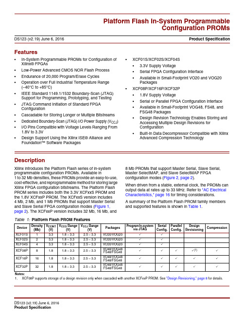
• Endurance of 20,000 Program/Erase Cycles
• Operation over Full Industrial Temperature Range (–40°C to +85°C)
DS123 (v2.19) June 6, 2016
Platform Flash In-System Programmable Configuration PROMs
Product Specification
Features
• In-System Programmable PROMs for Configuration of Xilinx® FPGAs
• Available in Small-Footprint VO20 and VOG20 Packages
• XCF08P/XCF16P/XCF32P
• 1.8V Supply Voltage
• Serial or Parallel FPGA Configuration Interface
• Available in Small-Footprint VOG48, FS48, and FSG48 Packages
–
+3.3V Supply. Positive 3.3V supply voltage for internal logic.
18
+3.3V, 2.5V, or 1.8V I/O Supply. Positive 3.3V, 2.5V, or 1.8V
–
supply voltage connected to the output voltage drivers and
信捷XC3系列PLC特殊寄存器一览表
M8000 运行常ON线圈M8001 运行常OFF线圈M8002 初始正向脉冲线圈M8003 初始负向脉冲线圈M8005 电池电压过低M8011 10ms 时钟脉冲: 5ms ON 5ms OFF M8012 100ms 时钟脉冲: 50msON 50msOFF M8013 1s 时钟脉冲:M8014 1min 时钟脉冲: 30sON 30s OFF M8018 年的位数:缺省为OFF(OFF:2 ON:4) M8020 零标志:加减运算结果为0时M8021 借位标志:减法运算发生借位M8022 进位标志:加法运算发生进位M8026 RAMP模式M8027 PR模式M8030 PLC初始化M8031 非保持寄存器清除M8032 保持寄存器清除M8033 存储器保持停止M8034 所有输出禁止M8038 通讯参数设定M8045 所有输出复位禁止M8046 STL状态动作M8050 禁止输入中断0M8051 禁止输入中断1M8052 禁止输入中断2M8053 禁止输入中断3M8054 禁止输入中断4M8055 禁止输入中断5M8056 禁止定时中断0M8057 禁止定时中断1M8058 禁止定时中断2M8059 禁止所有中断M8067 运算错误M8070 扫描超时M8071 没有用户程序M8072 用户程序错误M8122 串口1RS232正在发送标志M8124 串口1RS232正在接收标志M8125 串口1接收不完整标志M8127 串口1接收错误标志M8128 串口1接收正确标志M8132 串口2RS232正在发送标志M8134 串口2RS232正在接收标志M8135 串口2接收不完整标志M8137 串口2通讯错误结束信号M8138 串口2通讯正常结束信号M8142 串口3RS232正在发送标志M8144 串口3RS232正在接收标志M8145 串口3接收不完整标志M8147 串口3通讯错误结束信号M8148 串口3通讯正常结束信号M8150 C600计数完成标志(24段)M8151 C602计数完成标志(24段)M8152 C604计数完成标志(24段)M8153 C606计数完成标志(24段)M8154 C608计数完成标志(24段)M8155 C610计数完成标志(24段)M8156 C612计数完成标志(24段)M8157 C614计数完成标志(24段)M8158 C616计数完成标志(24段)M8159 C618计数完成标志(24段)M8160 C620计数完成标志(24段)M8161 C622计数完成标志(24段)M8162 C624计数完成标志(24段)M8163 C626计数完成标志(24段)M8164 C628计数完成标志(24段)M8165 C630计数完成标志(24段)M8166 C632计数完成标志(24段)M8167 C634计数完成标志(24段)M8168 C636计数完成标志(24段)M8169 C638计数完成标志(24段)M8170 Y0正在发出脉冲标志M8171 32位脉冲发送溢出标志M8172 方向标志1为正向,对应输出口为ON M8173 PULSE_2正在发出脉冲标志M8174 32位脉冲发送溢出标志M8175 方向标志1为正向,对应输出口为ON M8176 PULSE_3正在发出脉冲标志M8177 32位脉冲发送溢出标志M8178 方向标志1为正向,对应输出口为ON M8179 PULSE_4正在发出脉冲标志M8180 32位脉冲发送溢出标志M8181 方向标志1为正向,对应输出口为ON M8238 C300~C498计数控制 0为加,1为减D8002 寄存器容量D8005 PLC内部电池电压D8010 当前扫描周期:为单位D8011 扫描时间的最小值:为单位D8012 扫描时间的最大值:为单位D8013 万年历时钟秒:0-59D8014 万年历时钟分钟:0-59D8015 万年历时钟小时:0-23D8016 万年历时钟日:1-31D8017 万年历时钟月:1-12D8018 万年历时钟年:00-99D8019 万年历时钟星期:日-6D8021 机型(低8)系列号(高8)D8022 兼容系统版本号(低)系统版本号(高) D8023 兼容机型版本号(低)机型版本号(高) D8024 机型信息D8025 机型信息D8026 机型信息D8027 适用的上位机版本D8028 适用的上位机版本D8029 适用的上位机版本D8067 运算错误代码序号(除0错)D8068 锁存发生错误代码序号D8070 超时的扫描时间(1ms单位)D8074 偏移寄存器D的编号D8123 串口1RS232接收数据数D8127 串口1通讯错误代码D8133 串口2RS232接收数据数D8137 串口2通讯错误代码D8143 串口3RS232接收数据数D8147 串口3通讯错误代码D8150 C600当前段(表示第n段)D8151 C602当前段(表示第n段)D8152 C604当前段(表示第n段)D8153 C606当前段(表示第n段)D8154 C608当前段(表示第n段)D8155 C610当前段(表示第n段)D8156 C612当前段(表示第n段)D8157 C614当前段(表示第n段)D8158 C616当前段(表示第n段)D8159 C618当前段(表示第n段)D8160 C620当前段(表示第n段)D8161 C622当前段(表示第n段)D8162 C624当前段(表示第n段)D8163 C626当前段(表示第n段)D8164 C628当前段(表示第n段)D8165 C630当前段(表示第n段)D8166 C632当前段(表示第n段)D8167 C634当前段(表示第n段)D8168 C636当前段(表示第n段)D8169 C638当前段(表示第n段)D8170 PULSE_1累计脉冲个数低16位D8171 PULSE_1累计脉冲个数高16位D8172 PULSE_1当前段(表示第n段)D8173 PULSE_2累计脉冲个数低16位D8174 PULSE_2累计脉冲个数高16位D8175 PULSE_2当前段(表示第n段)D8176 PULSE_3累计脉冲个数低16位D8177 PULSE_3累计脉冲个数高16位D8178 PULSE_3当前段(表示第n段)D8179 PULSE_4累计脉冲个数低16位D8180 PULSE_4累计脉冲个数高16位D8181 PULSE_4当前段(表示第n段)D8190 PULSE_1当前次脉冲个数低16位D8191 PULSE_1当前次脉冲个数高16位D8192 PULSE_2当前次脉冲个数低16位D8193 PULSE_2当前次脉冲个数高16位D8194 PULSE_3当前次脉冲个数低16位D8195 PULSE_3当前次脉冲个数高16位D8196 PULSE_4当前次脉冲个数低16位D8197 PULSE_4当前次脉冲个数高16位FD8000 X端口输入滤波时间(单位ms) FD8010 X00对应输入映像I**的编号FD8011 X01对应输入映像I**的编号FD8012 X02对应输入映像I**的编号FD8013 X03对应输入映像I**的编号FD8014 X04对应输入映像I**的编号FD8015 X05对应输入映像I**的编号FD8016 X06对应输入映像I**的编号FD8017 X07对应输入映像I**的编号FD8018 X10对应输入映像I**的编号FD8019 X11对应输入映像I**的编号FD8020 X12对应输入映像I**的编号FD8021 X13对应输入映像I**的编号FD8022 X14对应输入映像I**的编号FD8023 X15对应输入映像I**的编号FD8024 X16对应输入映像I**的编号FD8025 X17对应输入映像I**的编号FD8026 X20对应输入映像I**的编号FD8027 X21对应输入映像I**的编号FD8028 X22对应输入映像I**的编号FD8030 X24对应输入映像I**的编号FD8031 X25对应输入映像I**的编号FD8032 X26对应输入映像I**的编号FD8033 X27对应输入映像I**的编号FD8034 X30对应输入映像I**的编号FD8035 X31对应输入映像I**的编号FD8036 X32对应输入映像I**的编号FD8037 X33对应输入映像I**的编号FD8038 X34对应输入映像I**的编号FD8039 X35对应输入映像I**的编号FD8040 X36对应输入映像I**的编号FD8041 X37对应输入映像I**的编号FD8042 X40对应输入映像I**的编号FD8043 X41对应输入映像I**的编号FD8044 X42对应输入映像I**的编号FD8045 X43对应输入映像I**的编号FD8046 X44对应输入映像I**的编号FD8047 X45对应输入映像I**的编号FD8048 X46对应输入映像I**的编号FD8049 X47对应输入映像I**的编号FD8050 X50对应输入映像I**的编号FD8051 X51对应输入映像I**的编号FD8052 X52对应输入映像I**的编号FD8053 X53对应输入映像I**的编号FD8054 X54对应输入映像I**的编号FD8055 X55对应输入映像I**的编号FD8056 X56对应输入映像I**的编号FD8057 X57对应输入映像I**的编号FD8058 X60对应输入映像I**的编号FD8059 X61对应输入映像I**的编号FD8060 X62对应输入映像I**的编号FD8061 X63对应输入映像I**的编号FD8062 X64对应输入映像I**的编号FD8063 X65对应输入映像I**的编号FD8064 X66对应输入映像I**的编号FD8065 X67对应输入映像I**的编号FD8066 X70对应输入映像I**的编号FD8067 X71对应输入映像I**的编号FD8068 X72对应输入映像I**的编号FD8069 X73对应输入映像I**的编号FD8070 X74对应输入映像I**的编号FD8071 X75对应输入映像I**的编号FD8072 X76对应输入映像I**的编号FD8074 Y00对应输出映像O**的编号FD8075 Y01对应输出映像O**的编号FD8076 Y02对应输出映像O**的编号FD8077 Y03对应输出映像O**的编号FD8078 Y04对应输出映像O**的编号FD8079 Y05对应输出映像O**的编号FD8080 Y06对应输出映像O**的编号FD8081 Y07对应输出映像O**的编号FD8082 Y10对应输出映像O**的编号FD8083 Y11对应输出映像O**的编号FD8084 Y12对应输出映像O**的编号FD8085 Y13对应输出映像O**的编号FD8086 Y14对应输出映像O**的编号FD8087 Y15对应输出映像O**的编号FD8088 Y16对应输出映像O**的编号FD8089 Y17对应输出映像O**的编号FD8090 Y20对应输出映像O**的编号FD8091 Y21对应输出映像O**的编号FD8092 Y22对应输出映像O**的编号FD8093 Y23对应输出映像O**的编号FD8094 Y24对应输出映像O**的编号FD8095 Y25对应输出映像O**的编号FD8096 Y26对应输出映像O**的编号FD8097 Y27对应输出映像O**的编号FD8098 Y30对应输出映像O**的编号FD8099 Y31对应输出映像O**的编号FD8100 Y32对应输出映像O**的编号FD8101 Y33对应输出映像O**的编号FD8102 Y34对应输出映像O**的编号FD8103 Y35对应输出映像O**的编号FD8104 Y36对应输出映像O**的编号FD8105 Y37对应输出映像O**的编号FD8106 Y40对应输出映像O**的编号FD8107 Y41对应输出映像O**的编号FD8108 Y42对应输出映像O**的编号FD8109 Y43对应输出映像O**的编号FD8110 Y44对应输出映像O**的编号FD8111 Y45对应输出映像O**的编号FD8112 Y46对应输出映像O**的编号FD8113 Y47对应输出映像O**的编号FD8114 Y50对应输出映像O**的编号FD8115 Y51对应输出映像O**的编号FD8116 Y52对应输出映像O**的编号FD8118 Y54对应输出映像O**的编号FD8119 Y55对应输出映像O**的编号FD8120 Y56对应输出映像O**的编号FD8121 Y57对应输出映像O**的编号FD8122 Y60对应输出映像O**的编号FD8123 Y61对应输出映像O**的编号FD8124 Y62对应输出映像O**的编号FD8125 Y63对应输出映像O**的编号FD8126 Y64对应输出映像O**的编号FD8127 Y65对应输出映像O**的编号FD8128 Y66对应输出映像O**的编号FD8129 Y67对应输出映像O**的编号FD8130 Y70对应输出映像O**的编号FD8131 Y71对应输出映像O**的编号FD8132 Y72对应输出映像O**的编号FD8133 Y73对应输出映像O**的编号FD8134 Y74对应输出映像O**的编号FD8135 Y75对应输出映像O**的编号FD8136 Y76对应输出映像O**的编号FD8137 Y77对应输出映像O**的编号FD8138 X00输入属性 0:常开 1:常闭FD8139 X01输入属性 0:常开 1:常闭FD8140 X02输入属性 0:常开 1:常闭FD8141 X03输入属性 0:常开 1:常闭FD8142 X04输入属性 0:常开 1:常闭FD8143 X05输入属性 0:常开 1:常闭FD8144 X06输入属性 0:常开 1:常闭FD8145 X07输入属性 0:常开 1:常闭FD8146 X10输入属性 0:常开 1:常闭FD8147 X11输入属性 0:常开 1:常闭FD8148 X12输入属性 0:常开 1:常闭FD8149 X13输入属性 0:常开 1:常闭FD8150 X14输入属性 0:常开 1:常闭FD8151 X15输入属性 0:常开 1:常闭FD8152 X16输入属性 0:常开 1:常闭FD8153 X17输入属性 0:常开 1:常闭FD8154 X20输入属性 0:常开 1:常闭FD8155 X21输入属性 0:常开 1:常闭FD8156 X22输入属性 0:常开 1:常闭FD8157 X23输入属性 0:常开 1:常闭FD8158 X24输入属性 0:常开 1:常闭FD8159 X25输入属性 0:常开 1:常闭FD8160 X26输入属性 0:常开 1:常闭FD8161 X27输入属性 0:常开 1:常闭FD8162 X30输入属性 0:常开 1:常闭FD8163 X31输入属性 0:常开 1:常闭FD8164 X32输入属性 0:常开 1:常闭FD8165 X33输入属性 0:常开 1:常闭FD8166 X34输入属性 0:常开 1:常闭FD8167 X35输入属性 0:常开 1:常闭FD8168 X36输入属性 0:常开 1:常闭FD8169 X37输入属性 0:常开 1:常闭FD8170 X40输入属性 0:常开 1:常闭FD8171 X41输入属性 0:常开 1:常闭FD8172 X42输入属性 0:常开 1:常闭FD8173 X43输入属性 0:常开 1:常闭FD8174 X44输入属性 0:常开 1:常闭FD8175 X45输入属性 0:常开 1:常闭FD8176 X46输入属性 0:常开 1:常闭FD8177 X47输入属性 0:常开 1:常闭FD8178 X50输入属性 0:常开 1:常闭FD8179 X51输入属性 0:常开 1:常闭FD8180 X52输入属性 0:常开 1:常闭FD8181 X53输入属性 0:常开 1:常闭FD8182 X54输入属性 0:常开 1:常闭FD8183 X55输入属性 0:常开 1:常闭FD8184 X56输入属性 0:常开 1:常闭FD8185 X57输入属性 0:常开 1:常闭FD8186 X60输入属性 0:常开 1:常闭FD8187 X61输入属性 0:常开 1:常闭FD8188 X62输入属性 0:常开 1:常闭FD8189 X63输入属性 0:常开 1:常闭FD8190 X64输入属性 0:常开 1:常闭FD8191 X65输入属性 0:常开 1:常闭FD8192 X66输入属性 0:常开 1:常闭FD8193 X67输入属性 0:常开 1:常闭FD8194 X70输入属性 0:常开 1:常闭FD8195 X71输入属性 0:常开 1:常闭FD8196 X72输入属性 0:常开 1:常闭FD8197 X73输入属性 0:常开 1:常闭FD8198 X74输入属性 0:常开 1:常闭FD8199 X75输入属性 0:常开 1:常闭FD8200 X76输入属性 0:常开 1:常闭FD8201 X77输入属性 0:常开 1:常闭FD8202 D断电保存区域起始标号FD8203 M断电保存区域起始标号FD8204 T断电保存区域起始标号FD8205 C断电保存区域起始标号FD8206 S断电保存区域起始标号FD8210 通讯口1通讯模式和站号FD8211 通讯口1通讯格式FD8212 通讯口1字符超时判断时间(ms) FD8213 通讯口1回复超时判断时间(ms) FD8214 通讯口1起始符(高8位无效) FD8215 通讯口1终止符(高8位无效) FD8216 通讯口1自由格式设置FD8220 通讯口2通讯模式和站号FD8221 通讯口2通讯格式FD8222 通讯口2字符超时判断时间(ms) FD8223 通讯口2回复超时判断时间(ms) FD8224 通讯口2起始符(高8位无效) FD8225 通讯口2终止符(高8位无效) FD8226 通讯口2自由格式设置FD8230 通讯口3通讯模式和站号FD8231 通讯口3通讯格式FD8232 通讯口3字符超时判断时间(ms) FD8233 通讯口3回复超时判断时间(ms) FD8234 通讯口3起始符(高8位无效) FD8235 通讯口3终止符(高8位无效) FD8236 通讯口3自由格式设置FD8892 0轴脉冲率FD8894 1轴脉冲率FD8896 2轴脉冲率FD8898 3轴脉冲率FD8900 0轴电机分辨率FD8902 1轴电机分辨率FD8904 2轴电机分辨率FD8906 3轴电机分辨率FD8908 设定频率(hz)FD8910 上升时间(ms)FD8912 下降时间(ms)FD8914 0轴电气原点FD8916 1轴电气原点FD8918 2轴电气原点FD8920 3轴电气原点FD8922 0轴机械原点FD8924 1轴机械原点FD8926 2轴机械原点FD8928 3轴机械原点FD8930 回机械原点速度(hz)FD8932 回机械原点爬行速度(hz)FD8934 0轴回机械零点Z向脉冲个数FD8935 1轴回机械零点Z向脉冲个数FD8936 2轴回机械零点Z向脉冲个数FD8937 3轴回机械零点Z向脉冲个数FD8938 回机械原点设定寄存器FD8942 0轴AB相反馈脉冲率FD8944 1轴AB相反馈脉冲率FD8946 2轴AB相反馈脉冲率FD8948 3轴AB相反馈脉冲率FD8950 随动前馈比例FD8952 0轴AB相反馈分辨率FD8954 1轴AB相反馈分辨率FD8956 2轴AB相反馈分辨率FD8958 3轴AB相反馈分辨率FD8960 追踪设定参数模式FD8961 刀辊周长(允许移动范围2Lm)FD8963 同步区长度(随动段(2L))FD8965 "料件位置信息X"的编码器每转脉冲数FD8966 "追件位置信息Ycur"的编码器每转的脉冲数(AB向反馈) FD8967 "追件控制信息"的电机每转的脉冲数(驱动轴)FD8968 "料件位置信息X"的编码器每转的单位距离FD8969 "追件位置信息Ycur"的编码器每转的单位距离(AB向反馈) FD8970 "追件控制信息"的电机每转的单位距离(驱动轴)FD8971 追件校准信号传感器距中心点的距离dadjFD8973 料件标记信号距追件校准信号的距离dmarkFD8975 追件最大加速度VMax(单位长度/S)FD8977 追件加减速时间(ms)FD8978 学习时追件速度VLearn(单位长度/S)FD8979 前馈参数FD8980 飞锯时主轴脉冲输出方向信号YnFD8981 停止位置FD8983 刀的数量(未开放)FD8984 刀与滚刀的夹角(未开放)FD8985 料件反馈位置信息电机每转脉冲数FD8986 料件反馈位置信息X"的电机每转的距离。
ADVFC32及应用

电压频率和频率电压转换器ADVFC32及应用一、概述ADVFC32是ADI公司生产的一种低成本的单片集成的实现电压频率转换或频率电压转换的器件。
它具有很好的线性(10KHz时的最大误差时0.01%),最大的工作频率可以达到0.5MHz。
只需要外接很少的器件就可以把输入的正、负电压或电流转换为与之成比例的频率。
频率电压转换的模式所用的器件与电压频率转换的相同,只是要有一个简单的逻辑偏压或网络组合来保证输入逻辑电平有较大的范围。
在V/F模式下用一个开放的输出频率收集器可以实现TTL和CMOS兼容。
上拉电阻可以接到30V、15V的电压,或者5V标准CMOS和TTL逻辑电平。
应选取这个电阻值限制输出集电极的电流不超过8毫安。
低输入电压失调漂移,仅有满度的3ppm/℃。
ADVFC32具有以下的一些优点:1、ADVFC32采用的是电荷平衡电路技术,这使得它的电压频率转换具有很高的精度。
它的工作频率的范围仅仅由一个精密电阻和电容决定,其它的元件对频率范围影响不大。
所以可以采用比较便宜的,精度±20%的电阻和电容,这样并不会影响线性和温度漂移。
2、ADVFC32可以很容易满足系统工作范围要求。
选择不同的输入电阻可以实现不同的输入电压缩放比。
输入电阻还可以在最大的输入电压时使输入电流达到0.25mA。
3、频率电压转换的模式所用的器件与电压频率转换的相同,只是要有一个简单的逻辑偏置、网络相加和重新组合即可。
4、ADVFC32和其它公司生产的VFC32具有引脚的兼容性。
5、ADVFC32与军用标准MIL_STD_883兼容。
二、封装结构ADVFC32有两种封装方式:一种是14管脚的双列直插式,另一种是10管脚的金属罐式。
图1(A)给出的是ADVFC32的14脚封装结构及引脚排布,图1(B)给出的是ADVFC32的10脚封装结构及引脚排布。
(A):14引脚封装结构(B ):10引脚封装结构图1:ADVFC32的两种封装结构三、工作原理及应用设计ADVFC32应用广泛,除了用于电压频率转换和频率电压转换,还可以用于微处理器控制的A/D 转换及其他的电路。
N32G4FRxC xE 数据手册说明书

N32G4FRxC/xE数据手册N32G4FR系列采用32 bit ARM Cortex-M4F内核,最高工作主频144MHz,支持浮点运算和DSP指令,集成多达512KB Flash,可用于安全存储指纹信息,144KB SRAM,2x12bit 5Msps ADC,2x1Msps 12bit DAC,集成多路U(S)ART、I2C、SPI、QSPI、USB、CAN通信接口,1xSDIO接口,数字摄像头(DVP)接口,支持主流的半导体指纹及光学传指纹感器,内置密码算法硬件加速引擎关键特性●内核CPU―32位ARM Cortex-M4 内核+ FPU,单周期硬件乘除法指令,支持DSP指令和MPU―内置8KB 指令Cache缓存,支持Flash加速单元执行程序0 等待―最高主频144MHz,180DMIPS●加密存储器―高达512KByte片内Flash,支持加密存储、多用户分区管理及数据保护,支持硬件ECC校验,10万次擦写次数,10年数据保持―144KByte片内SRAM(包含16KByte Retention RAM),Retention RAM支持硬件奇偶校验●时钟―HSE:4MHz~32MHz外部高速晶体―LSE:32.768KHz外部低速晶体―HSI:内部高速RC OSC 8MHz―LSI:内部低速RC OSC 40KHz―内置高速PLL―支持1路时钟输出,可配置系统时钟、HSE、HSI或PLL后分频输出●复位―支持上电/掉电/欠压/外部引脚复位―支持看门狗复位,软件复位●通信接口―7个U(S)ART接口, 最高速率达4.5 Mbps,其中3个USART接口(支持ISO7816,IrDA,LIN),4个UART接口―3个SPI接口,速率高达36 MHz,其中2个支持I2S―1个QSPI接口,速率高达144 Mbps―4个I2C接口,速率高达1 MHz,主从模式可配,从机模式下支持双地址响应―1个USB2.0 Full Speed Device接口―2个CAN 2.0A/B总线接口―1个SDIO接口,支持SD/MMC格式―1个DVP (Digital Video Port)接口●高性能模拟接口―2个12bit 5Msps高速ADC,可配置为12/10/8/6bit模式,6bit 模式下采样率高达9Msps,多达16路外部单端输入通道,支持差分模式―2个12bit DAC,采样率1Msps―支持外部输入独立参考电压源―所有模拟接口支持1.8~3.6V全电压工作●最大支持65个支持复用功能的GPIOs,大多数GPIO支持5V耐压.●2个高速DMA控制器,每个控制器支持8通道,通道源地址及目的地址任意可配●RTC实时时钟,支持闰年万年历,闹钟事件,周期性唤醒,支持内外部时钟校准●定时计数器― 2 个16bit高级定时计数器,支持输入捕获、输出比较、PWM输出以及正交编码输入等功能,最高控制精度6.9ns。
FPGA可编程逻辑器件芯片XC3S100E-5FG484C中文规格书
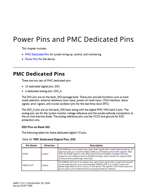
Power Pins and PMC Dedicated Pins This chapter includes:•PMC Dedicated Pins for system bring-up, control, and monitoring•Power Pins for the devicePMC Dedicated PinsThere are two sets of PMC dedicated pins:•15 dedicated digital pins, DIO• 4 dedicated analog pins, DIO_AThe DIO pins are on the bank_503 package bank. These pins provide functions such as bootmode selection, external reference clock input, power-on reset input, JTAG interface, statussignals, error signals, and crystal oscillator pins for the real-time clock (RTC).The DIO_A pins are on the bank_500 bank along with the digital PMC MIO bank 0 pins. Theanalog pins are for the system monitor voltage reference and the anode/cathode connections to the on-chip thermal diode. The analog reference pins use the VCCO and ground for ESDprotection only.DIO Pins on Bank 503The following table lists these dedicated digital I/O pins.Table 42: PMC Dedicated Digital Pins, DIOPin Name Direction DescriptionDONE Output The DONE pin is an output-only, open-drain signal with a weak internal pull-up. An external pull-up is recommended. DONE is controlled by the DONE register. After POR, the DONE signal is Low. When the PLM successfully completes the boot sequence, the software sets the [DONE] bit High, which causes the output buffer to float and be pulled High externally.ERROR_OUT Output The ERROR_OUT pin is an output-only, open-drain signal with a weak internal pull-up. An external pull-up is recommended. ERROR_OUT is in a High-Z state and pulled High when an error occurs in the device. The specific errors that cause this pin to assert can be determined and programmed by software.Section V: Signals, Interfaces, Pins, and ControlsChapter 21: Power Pins and PMC Dedicated PinsSection IV: Address Maps and Programming InterfacesChapter 20: Programming Interfaces The memory-mapped registers are accessed using 32-bit words as described in ProgrammingInterfaces.The programming registers for the blocks in the PMC, PS, and CPM are accessed using 32-bitR/W transactions to APB programming interface ports on each unit. The AXI interconnect ofeach subsystem has an APB switch that connects to the APB programming interface of thefunctional units. Interrupts are signaled directly to the system interrupt controllers in the FPD,LPD, PMC, and to the PL fabric.Address MapsThe APB, AXI interfaces are divided into several address maps for the FPD, LPD, and PMC.AccessibilityThe accessibility of the APB programming interfaces depends on the configuration of the XPPUs that are protecting them.Memory-mapped Register Access TypesThe memory-mapped (MM) register can be read, write, or have another access type as shown in the following table.Table 41: Memory-mapped Register Access TypesAccess Type DescriptionR Read-onlyW Write-onlyRW Read or writeWTC or W1C Write 1 to clear (readable unless noted)NPI Programming InterfaceThe NoC structure includes a register programming interface (NPI) to configure the NoCcomponents, AI Engine, DDR memory controller, and integrated hardware peripherals in the PL.The NPI also transports interrupts from the subsystem unit back to the NPI controller where they are signaled as system interrupts.The host NPI controller is accessible on the PMC AXI main switch. Accesses to the NPI host and the programming interfaces attached to it are accessed through the NPI_XPPU protection unit.The NPI bus structure is in the SoC power domain, same as the NoC, but it functions completely independently of the NoC interconnect. The NPI supports burst accesses to reduce registerprogramming time.Section IV: Address Maps and Programming InterfacesChapter 20: Programming InterfacesFeaturesThe NPI features include:•Read/write pathway to the programming control and status registers (PCSRs)•Burst read/write transactions•Ordered reads and writes•APB error interrupt (programming interface)Errors and InterruptsIf a subsystem unit detects an access error, or generates a system interrupt, it is signaled back to the NPI host controller. The interrupts are routed to the system interrupt controllers, includingthe RPU and APU GICs, the PMC system interrupt controller, and to PL outputs in the fabric. The errors are routed to the system error controller in the PMC and to PL outputs in the fabric.AccessibilityThe NPI controller is attached to the AXI main switch in the PMC. Accesses are monitored by the PMC_XPPU_NPI protection unit.Configuration Frame Programming Interface The PL adaptable engines, fabric, clocks, and integrated hardware is programmed usingconfiguration frames (CFRAME). The configuration frames are written to the configuration frame unit (CFU). The CFU receives data files and generates configuration packets out on to theconfiguration frame interface (CFI) to program the device.The PL building blocks are introduced in Programmable Logic with references to relateddocuments.。
VFC32BM资料
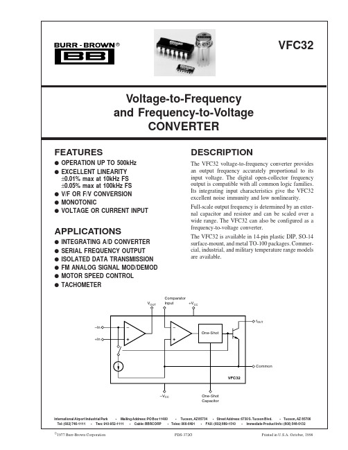
©1977 Burr-Brown Corporation PDS-372G Printed in U.S.A. October, 19982VFC32SPECIFICATIONSAt T A = +25°C and V CC = ±15V, unless otherwise noted.V Specification the same as VFC32KP.NOTES: (1) A 25% duty cycle (0.25mA input current) is recommended for best linearity. (2) Adjustable to zero. See Offset and Gain Adjustment section. (3) Linearity error is specified at any operating frequency from the straight line intersecting 90% of full scale frequency and 0.1% of full scale frequency. See Discussion of Specifications section. Above 200kHz,it is recommended all grades be operated below +85°C. (4) ±0.015% of FSR for negative inputs shown in Figure 5. Positive inputs are shown in Figure 1. (5) FSR = Full Scale Range (corresponds to full scale frequency and full scale input voltage). (6) Exclusive of external components’ drift. (7) Positive drift is defined to be increasing frequency with increasing temperature. (8) For operations above 200kHz up to 500kHz, see Discussion of Specifications and Installation and Operation sections. (9) One pulse of new frequency plus 1µs.3VFC32Supply Voltage...................................................................................±22V Output Sink Current (F OUT )................................................................50mA Output Current (V OUT )......................................................................+20mA Input Voltage, –Input.....................................................................±Supply Input Voltage, +Input.....................................................................±Supply Comparator Input ..........................................................................±Supply Storage Temperature Range:VFC32BM, SM.............................................................–65°C to +150°C VFC32KP, KU................................................................–25°C to +85°CABSOLUTE MAXIMUM RATINGSThe information provided herein is believed to be reliable; however, BURR-BROWN assumes no responsibility for inaccuracies or omissions. BURR-BROWN assumes no responsibility for the use of this information, and all use of such information shall be entirely at the user’s own risk. Prices and specifications are subject to change without notice. No patent rights or licenses to any of the circuits described herein are implied or granted to any third party. BURR-BROWN does not authorize or warrant any BURR-BROWN product for use in life support devices and/or systems.PIN CONFIGURATIONSThis integrated circuit can be damaged by ESD. Burr-Brown recommends that all integrated circuits be handled with appropriate precautions. Failure to observe proper handling and installation procedures can cause damage.ESD damage can range from subtle performance degradation to complete device failure. Precision integrated circuits may be more susceptible to damage because very small parametric changes could cause the device not to meet its published specifi-cations.PACKAGE DRAWING TEMPERATUREPRODUCT PACKAGE NUMBER (1)RANGE VFC32KP 14-Pin Plastic DIP 0100°C to 70°C VFC32BM TO-100 Metal 007–25°C to +85°C VFC32SM TO-100 Metal 007–55°C to +125°C VFC32KUSO-14 SOIC2350°C to +70°CNOTE: (1) For detailed drawing and dimension table, please see end of data sheet, or Appendix C of Burr-Brown IC Data Book.PACKAGE/ORDERING INFORMATION4VFC32TYPICAL PERFORMANCE CURVESAt T A = +25°C and V CC = ±15V, unless otherwise noted.1k1MFull Scale Frequency (Hz)0.100.001T y p i c a l L i n e a r i t y E r r o r (% o f F S R )10k100k0.01LINEARITY ERROR vs FULL SCALE FREQUENCY10kOperating Frequency (Hz)1–1.0L i n e a r i t y E r r o r (H z )1k7kLINEARITY ERROR vs OPERATING FREQUENCY2k3k4k5k6k8k9k0.5–0.51k1MFull Scale Frequency (Hz)100010F u l l S c a l e T e m p D r i f t (p p m o f F S R /°C )10k100k100FULL SCALE DRIFT vs FULL SCALE FREQUENCY5VFC32APPLICATION INFORMATIONFigure 1 shows the basic connection diagram for frequency-to-voltage conversion. R 1 sets the input voltage range. For a 10V full-scale input, a 40k Ω input resistor is recommended.Other input voltage ranges can be achieved by changing the value of R 1.R 1should be a metal film type for good stability. Manufac-turing tolerances can produce approximately ±10% variationin output frequency. Full-scale output frequency can be trimmed by adjusting the value of R 1—see Figure 3.The full-scale output frequency is determined by C 1. Values shown in Figure 1 are for a full-scale output frequency of 10kHz. Values for other full-scale frequencies can be read from Figure 2. Any variation in C 1—tolerance, temperature drift, aging—directly affect the output frequency. Ceramic NPO or silver-mica types are a good choice.For full-scale frequencies above 200kHz, use larger capaci-tor values as indicated in Figure 2, with R 1 = 20k Ω.The value of the integrating capacitor, C 2, does not directly influence the output frequency, but its value must be chosen within certain bounds. Values chosen from Figure 2 produceapproximately 2.5Vp-p integrator voltage waveform. If C 2’s value is made too low, the integrator output voltage can exceed its linear output swing, resulting in a nonlinear response. Using C 2 values larger than shown in Figure 2 is acceptable.Accuracy or temperature stability of C 2 is not critical be-cause its value does not directly affect the output frequency.For best linearity, however, C 2 should have low leakage and low dielectric absorption. Polycarbonate and other film capacitors are generally excellent. Many ceramic types are adequate, but some low-voltage ceramic capacitor types may degrade nonlinearity. Electrolytic types are not recom-mended.FREQUENCY OUTPUT PINThe frequency output terminal is an open-collector logic output. A pull-up resistor is usually connected to a 5V logic supply to create standard logic-level pulses. It can, however,be connected to any power supply up to +V CC . Output pulses have a constant duration and positive-going during the one-shot period. Current flowing in the open-collector output transistor returns through the Common terminal. This termi-nal should be connected to logic ground.(1)FIGURE 1. Voltage-to-Frequency Converter Circuit.R 1=V FS0.25mA6VFC32PRINCIPLES OF OPERATIONThe VFC32 operates on a principle of charge balance. The signal input current is equal to V IN /R 1. This current is integrated by input op amp and C 2, producing a downward ramping integrator output voltage. When the integrator out-put ramps to the threshold of the comparator, the one-shot is triggered. The 1mA reference current is switched to the integrator input during the one-shot period, causing the integrator output ramp upward. After the one-shot period,the integrator again ramps downward.The oscillation process forces a long-term balance of charge (or average current) between the input signal current and the reference current. The equation for charge balance is:Where:f O is the output frequencyt OS is the one-shot period, equal to t OS = 7500 C 1 (Farads)(4)The values suggested for R 1 and C 1 are chosen to produce a 25% duty cycle at full-scale frequency output. For full-scale frequencies above 200kHz, the recommended values pro-duce a 50% duty cycle.FREQUENCY-TO-VOLTAGE CONVERSION Figure 4 shows the VFC32 connected as a frequency-to-voltage converter. The capacitive-coupled input network C 3,R 6 and R 7 allow standard 5V logic levels to trigger the comparator input. The comparator triggers the one-shot on the falling edge of the frequency input pulses. Threshold voltage of the comparator is approximately –0.7V. For frequency input waveforms less than 5V logic levels, the R 6/R 7 voltage divider can be adjusted to a lower voltage to assure that the comparator is triggered.The value of C 1 is chosen from Figure 2 according to the full-scale input frequency. C 2 smooths the output voltage waveform. Larger values of C 2 reduce the ripple in the output voltage. Smaller values of C 2 allow the output voltage to settle faster in response to a change in input frequency.Resistor R 1 can be trimmed to achieve the desired output voltage at the full-scale input frequency.I IN =I R(AVERAGE)(2)V INR 1=f O t OS (1mA)(3)FIGURE 2. Capacitor Value Selection.FIGURE 3. Gain and Offset Voltage Trim Circuit.FIGURE 4. Frequency-to-Voltage Converter Circuit.FIGURE 5. V/F Converter—Negative Input Voltage.7VFC32。
FPGA可编程逻辑器件芯片XC3S400A-4FGG320C中文规格书
In the eMMC1 boot mode, the RCU BootROM runs at an eMMC1 device clock frequency between 8.7 MHz and 19.3 MHz dependent on the REF_CLK setting. The eMMC1 boot mode supports 1.8V and 1-bit, 4-bit, and 8-bit data interfaces. The BootROM uses auto-width detection to determine the data bus width for initial boot. The auto-bus width detection starts by checking the 8-bit data bus width, followed by 4-bit data bus width, and then 1-bit data bus width.Note: When connecting to the eMMC1 controller using a 1-bit data bus width, note the detection order because the remainder of the 8-bit data bus MIO data pins toggle during the initial bus-width detection. For additional information on the SD/eMMC controller, see SD/eMMC Controller. eMMC1 SignalsIn eMMC1 boot mode, the MIO[0, 3:12] are configured by the BootROM to use:•Default drive strength (8 mA)•Default slew rate (slow)•Default weak pull-ups (enabled)•Enables the Schmitt trigger•Disables the 3-state overrideThe remaining MIOs are not set by the BootROM and remain at their default state. If a secure lockdown occurs during boot, the BootROM sets the to 0xFFFFFFFF to 3-state all I/Os. See Versal ACAP Register Reference (AM012) for details.The following table lists the bidirectional PMC multiplexed I/Os (MIOs) and their functions used in the eMMC1 boot mode setup.Table 23: eMMC1 Boot Mode SignalsPMC MIO Pin Signal Name Description0EMMC1_CLK eMMC1 clock output3EMMC1_CMD eMMC1 command4EMMC1_DATA[0]Data pin used in eMMC1 boot mode (1-bit, 4-bit, 8-bit)5EMMC1_DATA[1]Data pin used in eMMC1 boot mode (4-bit, 8-bit)6EMMC1_DATA[2]Data pin used in eMMC1 boot mode (4-bit, 8-bit)7EMMC1_DATA[3]Data pin used in eMMC1 boot mode (4-bit, 8-bit)8EMMC1_DATA[4]Data pin used in eMMC1 boot mode (8-bit)9EMMC1_DATA[5]Data pin used in eMMC1 boot mode (8-bit)10EMMC1_DATA[6]Data pin used in eMMC1 boot mode (8-bit)11EMMC1_DATA[7]Data pin used in eMMC1 boot mode (8-bit)12EMMC1_RST Reset output that resets the eMMC flasheMMC1 InterfaceThe following figure shows an example setup for eMMC1 boot mode from a single flash device.Figure 26: eMMC1 Interface ExampleX22630-102020Octal SPI Boot ModeThe octal SPI (OSPI) boot mode has an SPI compatible serial bus interface with extended octal commands. The OSPI boot mode supports an 8-bit data bus width and single transfer rate (STR) during the RCU BootROM execution. The BootROM runs at an OSPI device clock frequencybetween 11 MHz and 24.5 MHz dependent on the REF_CLK setting.After the BootROMexecution, the PLM can support the double data rate (DDR) with strobe for higher performance.The OSPI boot mode can be configured to a OSPI single or dual-stacked setup. For additionalinformation on the OSPI controller, see Octal SPI Controller.Note: When using OSPI dual-stacked mode, the BootROM can only access the lower OSPI0 addressable flash memory space for boot. After boot, the PLM can access the upper OSPI1 for additional imagestorage.The following table lists the STR OSPI commands supported by the RCU BootROM.Table 24: OSPI Commands Supported by RCU for BootBoot Mode Data Width Read Command Command Code Dummy Cycles OSPI1Read03h-OSPI14-byte read13h-Table 24: OSPI Commands Supported by RCU for Boot (cont'd)Boot Mode Data Width Read Command Command Code Dummy Cycles OSPI84-byte octal output fast read7Ch8In OSPI boot mode, the device initiates the boot sequence with the default 4-byte address octal output fast read command code 7Ch and the BootROM searches for a valid boot header. If a valid boot header is not found, the Versal ACAP attempts to load the image using the 4-byte alternate addressing read command code 13h. If a valid boot header is still not detected, the basic read command 03h is tried. If the boot attempt is unsuccessful after the third command, the BootROM increments the image header address register by 32 KB and tries the OSPI command sequence again to locate a valid boot header. If the OSPI boot mode search limit is reached without a successful boot, the RCU goes into lockdown and the ERROR_OUT pin is set. The image search limit for each boot mode is listed in Table 15: Boot Mode Search Limit. Octal SPI SignalsIn OSPI boot mode, MIO[0:5, 7:12] are configured by the BootROM to use:•Default drive strength (8 mA)•Default slew rate (slow)•Default weak pull-ups (enabled)•Enables the Schmitt trigger•Disables the 3-state overrideThe remaining MIOs are not set by the BootROM and remain at their default state. If a secure lockdown occurs during boot, the BootROM sets the to 0xFFFFFFFF to 3-state all I/Os. See Versal ACAP Register Reference (AM012) for details.The following table lists the bidirectional PMC multiplexed I/Os (MIOs) and their functions used in the OSPI boot mode setup.Table 25: Octal SPI Boot Mode SignalsPMC_MIO Pin Signal Name Description0OSPI_CLK OSPI clock output for OSPI0 in single setup, or OSPI clock output for OSPI0 and OSPI1in dual-stacked setup.1OSPI_IO[0]Data pin used for OSPI single or dual-stacked boot mode setup2OSPI_IO[1]Data pin used for OSPI single or dual-stacked boot mode setup3OSPI_IO[2]Data pin used for OSPI single or dual-stacked boot mode setup4OSPI_IO[3]Data pin used for OSPI single or dual-stacked boot mode setup5OSPI_IO[4]Data pin used for OSPI single or dual-stacked boot mode setup。
FPGA可编程逻辑器件芯片XC7A35T-2FGG484C中文规格书
Chapter2 Power Distribution SystemThis chapter documents the power distribution system (PDS) for 7series FPGAs,including decoupling capacitor selection, placement, and PCB geometries. A simpledecoupling method is provided for each 7series FPGA. Basic PDS design principles arecovered, as well as simulation and analysis methods. This chapter contains the followingsections:•PCB Decoupling Capacitors•Basic PDS Principles•Simulation Methods•PDS Measurements•TroubleshootingPCB Decoupling CapacitorsRecommended PCB Capacitors per DeviceA simple PCB-decoupling network for the Spartan®-7devices is listed in Table2-1, for theArtix™-7devices in Table2-2, for the Kintex™-7 devices in Table2-3, and for theVirtex®-7devices in Table2-4.In Table2-1, Table2-2, Table2-3, and Table2-4, the optimized quantities of PCBdecoupling capacitors assume that the voltage regulators have stable output voltages andmeet the regulator manufacturer’s minimum output capacitance requirements.Decoupling methods other than those presented in these tables can be used, but thedecoupling network should be designed to meet or exceed the performance of the simpledecoupling networks presented here. The impedance of the alternate network must be lessthan or equal to that of the recommended network across frequencies from 100KHz to10MHz.Because device capacitance requirements vary with CLB and I/O utilization, PCBdecoupling guidelines are provided on a per-device basis based on very high utilization soas to cover a majority of use cases. Resource usage consists (in part) of:•80% of LUTs and registers at 245MHz•80% block RAM and DSP at 491MHz•50% MMCM and 25% PLL at 500MHz•100% I/O at SSTL 1.2/1.35 at 1,200/800MHzThe Xilinx Power Estimator (XPE) tool is used to estimate the current on each power rail.DS189, Spartan 7 FPGAs Data Sheet: DC and AC Switching Characteristics, DS181, Artix 7Chapter 2:Power Distribution SystemPCB Decoupling CapacitorsTable 2-2 lists the PCB decoupling capacitor guidelines per V CC supply rail for Artix-7devices.CSGA324XC7S5001351111123124FTGB196XC7S5001351111113124FGGA484XC7S5001351111124124FGGA484XC7S7501471111137124FGGA676XC7S7501471111137124FGGA484XC7S10001581111137124FGGA676XC7S1001581111137124Notes:1.PCB capacitor specifications are listed in Table 2-5.2.Total includes all capacitors for all supplies. The values in this table account for the number of I/O banks in the device.3.One 47µF (or 100µF) capacitor is required for up to four V CCO banks when powered by the same voltage.4.Decoupling capacitors cover down to approximately 100KHz.Table 2-1:Required PCB Capacitor Quantities per Device: Spartan-7Devices (1)(2) (Continued)PackageDeviceV CCINTV CCBRAMV CCAUXV CCO (per Bank)330µF 100µF 4.7µF 0.47µF 100µF 47µF 4.7µF 0.47µF 47µF 4.7µF 0.47µF47µF or100µF (3)4.7µF 0.47µFTable 2-2:Required PCB Capacitor Quantities per Device: Artix-7Devices (1)(2)PackageDeviceV CCINTV CCBRAM V CCAUXV CCO Bank 0V CCO all other Banks(per Bank)680µF 330µF 100µF 47µF 4.7µF 0.47µF 100µF 47µF 4.7µF 0.47µF 47µF 4.7µF 0.47µF 47µF47µF or100µF (3)4.7µF 0.47µFCPG238XC7A12T 00101201011121124CSG325XC7A12T 00101201011121124CPG236XC7A15TXA7A15T 0122111121124CPG238XC7A25T 00102301011121124CSG325XC7A25T 00102301011121124CPG236XC7A35T XA7A35T 0123111121124CPG236XC7A50T XA7A50T 01003510011121124FTG256XC7A15T 00102201011231124FTG256XC7A35T 00102301011231124FTG256XC7A50T 01003510011231124FTG256XC7A75T 01004610021231124FTG256XC7A100T 01006810021231124CSG324XC7A15T XA7A15T 0122111241124CSG324XC7A35T XA7A35T 00102301011241124CSG324XC7A50T XA7A50T01003510011241124Basic PDS PrinciplesSingle-Ended Signaling。
FPGA可编程逻辑器件芯片XC3S100E-5FGG484C中文规格书
Chapter 9Programmable LogicThe programmable logic (PL) is a scalable structure that provides the ability to create manypossible functions. The PL logic regions include DSP engines, configurable logic blocks, and two types of RAM arrays. These are configured together to create almost any type of hardwarefunctionality including accelerators, processors, functional pipeline units, and peripherals. The PL includes connections for the integrated hardware and peripherals, ports to the NoC interconnect,access to CMOS and gigabit high-speed I/O, and interface channels to the PS.The PL complements the functionality of the PS, AI Engine, and other integrated hardware to improve application performance. The PL instantiates system functionality and provides connectivity between the system and integrated hardware and peripherals.The PMC and PS have many signal connections and bus interfaces to the PL. These aresummarized in the Boundary Interface Signals chapter.PL ConfigurationThe connections and configuration of the PL elements are captured in the Vivado ® design suite and the Vitis ™ unified software platform tool chain using a programmable device image (PDI).The PDI contains PL configuration frames (CFRAME), which are sent by the PLM to theconfiguration frame unit (CFU) for processing. The CFU interfaces to the PL via the configuration frame interface (CFI). The PL can be configured during the boot process and can be re-configured during normal system operation. The PL configuration can be read-back for debug and functional safety applications. The CFU is described in Configuration Frame Unit and the CFI is described in Configuration Frame Interface .Building BlocksThe PL includes building blocks and provides several types of connections to many parts of the device including several subsystems and I/O. The PL has AXI interfaces to the PS, CPM, AI Engine, and the integrated controllers. The PL also has port interface signals and parameter configuration inputs to the PS, PMC, and other parts of the system.The PL building blocks include the DSP Engine, configurable logic block (CLB), Block RAM, and UltraRAM integrated components. These components are surrounded by clocking structures and wiring pathways. The PL makes connection between PS, CPM, PMC, NoC, AI Engine, GTs, XPIO banks, high-density I/O (HDIO) buffers, and components instantiated within the PL.The PL building blocks include:Section II: Hardware ArchitectureChapter 9: Programmable LogicAM011 (v1.1) November 30, 2020Versal ACAP TRM○ULPI is routed via the PMC MIO (not LPD MIO or EMIO)For more information, see Section XII: I/O Peripheral Controllers .Flash Memory ControllersThe flash memory controllers are located in the PMC and include:•Quad SPI Controller•Octal SPI Controller•SD/eMMC Controller (two in PMC)Flash memory controllers can serve as primary boot devices. The options are listed in Boot Modes .Section II: Hardware ArchitectureChapter 8: PS and PMC I/O PeripheralsAM011 (v1.1) November 30, 2020Versal ACAP TRM•DSP Engine (intelligent)•CLB (adaptable)•Block RAM and UltraRAM (adaptable)Additional FeaturesThe PL also contains clocking structures and PLL-enabled clocks for the PL fabric and I/O. The PL also includes connections to the Arm CoreSight™ debug hardware for data monitoring and collection.Tool SupportThe Vivado tools provide a large library of complex functional components (microprocessors,peripherals, filters, etc.) that can be instantiated and connected to create a design. Additionally, a hardware description language can be used to describe specific functions in the design. The Vivado tools then translate the design into the building blocks of the PL. The PL can be partially or fully programmed during the boot start-up and as a service operation when the system is operating.Block DiagramThe PL building blocks and clock structures provide the foundation for instantiating functionality.The PL is provided with port interface signals attached to nearly every part of the device.The high-level PL perspective of the system is shown in the following figure.Section II: Hardware ArchitectureChapter 9: Programmable LogicAM011 (v1.1) November 30, 2020Versal ACAP TRM。
FPGA可编程逻辑器件芯片XC3S4000-4FT256C中文规格书
Integrated 100G Ethernet Subsystem v2.6 PG165 February 4, 2021Appendix A:Auto-Negotiation and Link TrainingThe functions of each bit are defined in IEEE 802.3 Clause 72, “72.6.10.2 Training frame structure”. Their purpose is to communicate the adjustments of the transmit equalizer during the process of link training. The corresponding signal names are defined in Port Descriptions.Training SequenceThe training sequence consists of a Pseudo Random Bit Sequence (PRBS) of 4094 bits followed by two 0s, for a total of 4096 bits. The PRBS is transmitted at the line rate of 10.3125 Gb/s. The PRBS generator receives an 11-bit seed from an external source. Subsequent to the initial seed being loaded, the PRBS generator continues to run with no further intervention being required.The PRBS generator itself is implemented with a circuit that corresponds to this polynomial: G(x) = 1 + x9 + x11ReceiveThe receive block implements the frame alignment state diagram illustrated in IEEE 802.3, Clause 72, Figure 72-4.Frame Lock State MachineThe frame lock state machine searches for the frame marker, consisting of 16 consecutive 1s followed by 16 consecutive 0s. This functionality is fully specified in IEEE 802.3, Clause 72, Figure 72-4. When frame lock is achieved, the frame_lock signal is set to a value of TRUE.Received DataThe receiver outputs the control channel with the bit definitions defined in Table A-1 and Table A-2.If a DME error occurs during the reception of a particular DME frame, the control channel outputs are not updated but retain the value of the last received good DME frame. They are updated when the next good DME frame is received.Port DescriptionsAuto-Negotiation SignalsTable A-3 lists the additional signals available when the auto-negotiation feature is present.Integrated 100G Ethernet Subsystem v2.6 PG165 February 4, 2021Appendix A:Auto-Negotiation and Link TrainingTable A-3:Auto-Negotiation SignalsName I/O ClockDomain Descriptionctl_autoneg_enable I init_clk Enable signal for auto-negotiation.ctl_autoneg_bypass I init_clk This input disables auto-negotiation and bypasses the auto-negotiation function. When this input is asserted, auto-negotiation is turned off, but the PCS is connected to the output to allow operation.ctl_an_nonce_seed[7:0]I init_clk8-bit seed to initialize the nonce field polynomialgenerator.ctl_an_pseudo_sel I init_clk Selects the polynomial generator for the bit 49 random bit generator. If this input is 1, then the polynomial is x7+x6+1. When this input is Low, the polynomial is x7+x3+1.ctl_restart_negotiation I init_clk This input triggers a restart of theauto-negotiation, regardless of what state the circuit is currently in.ctl_an_local_fault I init_clk This input signal sets the local_fault bit of thetransmit link codeword.Signals Used for PAUSE Ability Advertisingctl_an_pause I init_clk This input sets the PAUSE bit, (C0), of the transmitlink codeword.ctl_an_asmdir I init_clk This input sets the ASMDIR bit, (C1), of thetransmit link codeword.ctl_an_loc_np I init_clk Local Next Page indicator. If this bit is 1, the ANIPC transfers the next page word at input loc_np_data to the remote link partner. If this bit is 0, the ANIPC does not initiate the next page protocol. If the link partner has next pages to send, and the loc_np bit is clear, the ANIPC transfers null message pages.ctl_an_loc_np_ack I init_clk Link Partner Next Page Acknowledge. This is used to signal the ANIPC that the next page data from the remote link partner at output pin lp_np_data has been read by the local host.When this signal goes High, the ANIPC acknowledges reception of the next page codeword to the remote link partner and initiates transfer of the next codeword. During this time, the ANIPC removes the lp_np signal until the new next page information is available.Integrated 100G Ethernet Subsystem v2.6PG165 February 4, 2021Appendix A:Auto-Negotiation and Link Training Ability Signal Inputs ctl_an_ability_1000base_kx I init_clkThese inputs identify the Ethernet protocol abilities that are advertised in the transmit link codeword to the link partner. A value of 1 indicates that the interface advertises that it supports the protocol.ctl_an_ability_10gbase_kr I init_clkctl_an_ability_10gbase_kx4I init_clkctl_an_ability_25gbase_krcr I init_clkctl_an_ability_25gbase_krcr_s I init_clkctl_an_ability_25gbase_kr1I init_clkctl_an_ability_25gbase_cr1I init_clkctl_an_ability_40gbase_cr4I init_clkctl_an_ability_40gbase_kr4I init_clkctl_an_ability_50gbase_cr2I init_clkctl_an_ability_50gbase_kr2I init_clkctl_an_ability_100gbase_cr10I init_clkctl_an_ability_100gbase_cr4I init_clkctl_an_ability_100gbase_kp4I init_clkctl_an_ability_100gbase_kr4I init_clkctl_an_cl91_fec_request I init_clkThis bit is used to request clause 91 FEC.ctl_an_cl91_fec_ability I init_clkThis bit is used to indicate clause 91 FEC ability.stat_an_link_cntl_10gbase_kx4[1:0]O init_clkLink Control outputs from the auto-negotiation controller auto-negotiation controller. The valid settings are as follows: •00: DISABLE; PCS is disconnected;•01: SCAN_FOR_CARRIER; RX is connected to PCS;•11: ENABLE; PCS is connected for mission mode operation.•"10: not used.stat_an_link_cntl_10gbase_kr[1:0]O init_clkstat_an_link_cntl_40gbase_kr4[1:0]O init_clkstat_an_link_cntl_40gbase_cr4[1:0]O init_clkstat_an_link_cntl_100gbase_cr10[1:0]O init_clkstat_an_link_cntl_100gbase_kp4[1:0]O init_clkstat_an_link_cntl_100gbase_kr4[1:0]O init_clkstat_an_link_cntl_100gbase_cr4[1:0]O init_clkstat_an_link_cntl_25gbase_krcr_s[1:0]O init_clkstat_an_link_cntl_25gbase_krcr[1:0]O init_clkstat_an_link_cntl_25gbase_kr1[1:0]O init_clkstat_an_link_cntl_25gbase_cr1[1:0]O init_clkstat_an_link_cntl_50gbase_kr2[1:0]O init_clkstat_an_lnk_cntl_50gbase_cr2[1:0]O init_clkstat_an_fec_enable Oinit_clk This output enables the use of clause 74 FEC on the link.Table A-3:Auto-Negotiation Signals (Cont’d)Name I/O Clock DomainDescription。
FPGA可编程逻辑器件芯片XC3S400A-5FG320C中文规格书
Register Descriptions 0x03D4STAT_RX_FRAMING_ERR_LANE9_MSB 0x03D8STAT_RX_FRAMING_ERR_LANE10_LSB 0x03DCSTAT_RX_FRAMING_ERR_LANE10_MSB 0x03E0STAT_RX_FRAMING_ERR_LANE11_LSB 0x03E4STAT_RX_FRAMING_ERR_LANE11_MSB 0x3E4 – 0x07FF ReservedTable 5-8:CORE_VERSION_REG Address BitsDefault Type Description 0x00007:0minor R Current version of the core in the format “major.minor”.For example, core version 1.9.Bits [7:0] represents minor version that is 9.Bits [15:8] represents major version that is 1.15:8major R 31:160NA Reserved Table 5-9:GT_RESET_REG AddressBits Default Type Description 0x000400RW gt_reset_all. A write of 1 issues a RESET to the GTs. This is a clear on write register.31:10NA ReservedTable 5-10:RESET_REG Address BitsDefault Type Description 0x000811:00RW usr_rx_serdes_reset. Unused PCS bits are RESERVED. A write of 1 in a given bit location puts that PCS lane logic into reset.120RW usr_tx_serdes_refclk_reset. A write of 1 puts the TX Serdes Refclk path in reset.29:130NA Reserved 300RW usr_rx_reset. RX core reset. A write of 1 puts the RX path in reset.310RW usr_tx_reset. TX core reset. A write of 1 puts the TX path in reset.Table 5-7:Status and Statistics Register Map (Cont’d)AddressRegister NameTable 5-11:CONFIGURATION_TX_REGAddress Bits Default Type Description0x000C 00RW ctl_tx_enable 8:10RW ctl_tx_mubits 31:90NA ReservedTable 5-12:CONFIGURATION_TX_DIAGWORD_REGAddress Bits Default Type Description0x001000RW ctl_tx_diagword_intfstat 12:10RW ctl_tx_diagword_lanestat 31:130NA ReservedTable 5-13:CONFIGURATION_RX_REGAddress Bits Default Type Description0x001400RW ctl_rx_force_resync 31:10NA ReservedTable 5-14:GT_LOOPBACK_REGAddress Bits Default Type Description0x001800RWaxi_gt_loopback0 is for Normal operation1 is for Near End PMA loopback 31:10NA ReservedTable 5-15:STAT_TX_STATUS_REGAddress Bits Default Type Description0x020000R/LH stat_tx_underflow_err10R/LH stat_tx_overflow_err20R/LH stat_tx_burst_err31R/LL stat_tx_errinj_biterr_done 31:40NA ReservedChapter 5:Example DesignTable 5-16:STAT_RX_STATUS_REGAddress Bits Default Type Description0x020401R/LL stat_rx_aligned. Default value is the value after reset. 10R/LH stat_rx_aligned_err20R/LH stat_rx_misaligned30R/LH stat_rx_msop_err40R/LH stat_rx_meop_err50R/LH stat_rx_burst_err60R/LH stat_rx_burstmax_err70R/LH stat_rx_overflow_err19:812’hFFF R/LL stat_rx_word_sync31:200NA ReservedTable 5-17:STAT_RX_DIAGWORD_REGAddress Bits Default Type Description0x020811:012’hFFF R/LL stat_rx_diagword_lanestat 23:1212’hFFF R/LL stat_rx_diagword_intfstat 31:240NA ReservedTable 5-18:STAT_RX_MUBITS_REGAddress Bits Default Type Description0x020C 7:00R/LH stat_rx_mubits 31:80NA ReservedTable 5-19:STAT_RX_SYNCED_REGAddress Bits Default Type Description0x021011:012’hFFF R/LL stat_rx_synced 31:120NA ReservedTable 5-20:STAT_RX_SYNCED_ERR_REGAddress Bits Default Type Description0x021411:00R/LH stat_rx_synced_err 31:120NA Reserved。
- 1、下载文档前请自行甄别文档内容的完整性,平台不提供额外的编辑、内容补充、找答案等附加服务。
- 2、"仅部分预览"的文档,不可在线预览部分如存在完整性等问题,可反馈申请退款(可完整预览的文档不适用该条件!)。
- 3、如文档侵犯您的权益,请联系客服反馈,我们会尽快为您处理(人工客服工作时间:9:00-18:30)。
CE
EN_EXT_SEL
OE/RESET BUSY
OSC
TCK TMS TDI TDO
Control and JTAG
Interface
Data Address
Memory
Data
Decompressor
Serial or
Parallel Interface
CLKOUT
CEO
DATA (D0) (Serial/Parallel Mode)
• XCF08P/XCF16P/XCF32P ♦ 1.8V supply voltage ♦ Serial or parallel FPGA configuration interface (up to 33 MHz) ♦ Available in small-footprint VO48, VOG48, FS48, and FSG48 packages ♦ Design revision technology enables storing and accessing multiple design revisions for configuration ♦ Built-in data decompressor compatible with Xilinx advanced compression technology
Parallel Config.
Design Revisioning
Compression
✓ ✓ ✓
✓
✓
✓
✓
✓
✓
✓
✓
✓
✓
✓
✓
✓
✓
✓
Description
Xilinx introduces the Platform Flash series of in-system programmable configuration PROMs. Available in 1 to 32 Megabit (Mbit) densities, these PROMs provide an easy-to-use, cost-effective, and reprogrammable method for storing large Xilinx FPGA configuration bitstreams. The Platform Flash PROM series includes both the 3.3V XCFxxS PROM and the 1.8V XCFxxP PROM. The XCFxxS version includes 4-Mbit, 2-Mbit, and 1-Mbit PROMs that
Table 1: Platform Flash PROM Features
Device Density VCCINT VCCO Range VCCJ Range
Packages
XCF01S XCF02S XCF04S
XCF08P
1 Mbit 2 Mbit 4 Mbit
8 Mbit
XCF16P 16 Mbit
© 2003-2006 Xilinx, Inc. All rights reserved. All Xilinx trademarks, registered trademarks, patents, and disclaimers are as listed at /legal.htm. PowerPC is a trademark of IBM, Inc. All other trademarks are the property of their respective owners. All specifications are subject to change without notice.
the PROMs DATA (D0-D7) pins. New data is available a short access time after each rising clock edge. The data is clocked into the FPGA on the following rising edge of the CCLK. A free-running oscillator can be used in the Slave Parallel /Slave SelecMAP mode.
元器件交易网
<BL Blue>
R
DS123 (v2.9) May 09, 2006
0
Features
• In-System Programmable PROMs for Configuration of Xilinx FPGAs
• Low-Power Advanced CMOS NOR FLASH Process
1.5V – 3.3V 2.5V – 3.3V
VO20/VOG20
VO20/VOG20
VO20/VOG20
VO48/VOG48 FS48/FSG48
VO48/VOG48 FS48/FSG48
VO48/VOG48 FS48/FSG48
Program In-system via JTAG
✓
✓
✓
Serial Config.
• JTAG Command Initiation of Standard FPGA Configuration
• Cascadable for Storing Longer or Multiple Bitstreams
• Dedicated Boundary-Scan (JTAG) I/O Power Supply (VCCJ)
• Endurance of 20,000 Program/Erase Cycles
• Operation over Full Industrial Temperature Range (–40°C to +85°C)
• IEEE Standard 1149.1/1532 Boundary-Scan (JTAG) Support for Programming, Prototyping, and Testing
XCF32P 32 Mbit
3.3V 3.3V 3.3V 1.8V
1.8V
1.8V
1.8V – 3.3V 2.5V – 3.3V 1.8V – 3.3V 2.5V – 3.3V 1.8V – 3.3V 2.5V – 3.3V 1.5V – 3.3V 2.5V – 3.3V
1.5V – 3.3V 2.5V – 3.3V
• I/O Pins Compatible with Voltage Levels Ranging From 1.5V to 3.3V
• Design Support Using the Xilinx Alliance ISE and Foundation ISE Series Software Packages
Data
and
Memory
JTAG Interface
Address
Data
Serial Interface
TDO
CEO
DATA (D0) Serial Mo Platform Flash PROM Block Diagram
ds123_01_30603
FI
CLK
Platform Flash In-System Programmable Configuration
PROMS
Product Specification
• XCF01S/XCF02S/XCF04S ♦ 3.3V supply voltage ♦ Serial FPGA configuration interface (up to 33 MHz) ♦ Available in small-footprint VO20 and VOG20 packages.
D[1:7] (Parallel Mode)
CF
REV_SEL [1:0]
Figure 2: XCFxxP Platform Flash PROM Block Diagram
ds123_19_122105
When the FPGA is in Master Serial mode, it generates a configuration clock that drives the PROM. With CF High, a short access time after CE and OE are enabled, data is available on the PROM DATA (D0) pin that is connected to the FPGA DIN pin. New data is available a short access time after each rising clock edge. The FPGA generates the appropriate number of clock pulses to complete the configuration.
The XCFxxP version of the Platform Flash PROM also supports Master SelectMAP and Slave SelectMAP (or Slave Parallel) FPGA configuration modes. When the FPGA is in Master SelectMAP mode, the FPGA generates a configuration clock that drives the PROM. When the FPGA is in Slave SelectMAP Mode, either an external oscillator generates the configuration clock that drives the PROM and the FPGA, or optionally, the XCFxxP PROM can be used to drive the FPGA’s configuration clock. With BUSY Low and CF High, after CE and OE are enabled, data is available on