35507-0800;中文规格书,Datasheet资料
MRF7S35015HSR3;MRF7S35015HSR5;中文规格书,Datasheet资料
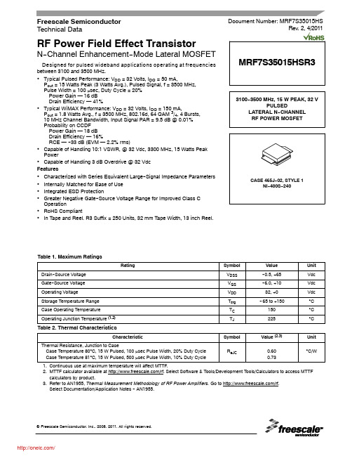
RF Power Field Effect TransistorN--Channel Enhancement--Mode Lateral MOSFETDesigned for pulsed wideband applications operating at frequencies between 3100and 3500MHz.•Typical Pulsed Performance:V DD =32Volts,I DQ =50mA,P out =15Watts Peak (3Watts Avg.),Pulsed Signal,f =3500MHz,Pulse Width =100μsec,Duty Cycle =20%Power Gain —16dB Drain Efficiency —41%•Typical WiMAX Performance:V DD =32Volts,I DQ =150mA,P out =1.8Watts Avg.,f =3500MHz,802.16d,64QAM 3/4,4Bursts,10MHz Channel Bandwidth,Input Signal PAR =9.5dB @0.01%Probability on CCDF Power Gain —18dB Drain Efficiency —16%RCE —--33dB (EVM —2.2%rms)•Capable of Handling 10:1VSWR,@32Vdc,3300MHz,15Watts Peak Power•Capable of Handling 3dB Overdrive @32Vdc Features•Characterized with Series Equivalent Large--Signal Impedance Parameters •Internally Matched for Ease of Use •Integrated ESD Protection•Greater Negative Gate--Source Voltage Range for Improved Class C Operation•RoHS Compliant•In Tape and Reel.R3Suffix =250Units,32mm Tape Width,13inch Reel.Table 1.Maximum RatingsRatingSymbol Value Unit Drain--Source Voltage V DSS --0.5,+65Vdc Gate--Source Voltage V GS --6.0,+10Vdc Operating VoltageV DD 32,+0Vdc Storage Temperature Range T stg --65to +150°C Case Operating Temperature T C 150°C Operating Junction Temperature (1,2)T J225°CTable 2.Thermal CharacteristicsCharacteristicSymbol Value (2,3)Unit Thermal Resistance,Junction to CaseCase Temperature 80°C,15W Pulsed,100μsec Pulse Width,20%Duty Cycle Case Temperature 81°C,15W Pulsed,500μsec Pulse Width,10%Duty CycleR θJC0.600.73°C/W1.Continuous use at maximum temperature will affect MTTF.2.MTTF calculator available at /rf.Select Software &Tools/Development Tools/Calculators to access MTTF calculators by product.3.Refer to AN1955,Thermal Measurement Methodology of RF Power Amplifiers.Go to /rf.Select Documentation/Application Notes --AN1955.Document Number:MRF7S35015HSRev.2,4/2011Freescale Semiconductor Technical DataMRF7S35015HSR3Table 3.ESD Protection CharacteristicsTest MethodologyClass Human Body Model (per JESD22--A114)1B (Minimum)Machine Model (per EIA/JESD22--A115)A (Minimum)Charge Device Model (per JESD22--C101)IV (Minimum)Table 4.Electrical Characteristics (T C =25°C unless otherwise noted)CharacteristicSymbolMinTypMaxUnitOff CharacteristicsGate--Source Leakage Current (V GS =5Vdc,V DS =0Vdc)I GSS ——1μAdc Zero Gate Voltage Drain Leakage Current (V DS =32Vdc,V GS =0Vdc)I DSS ——2μAdc Zero Gate Voltage Drain Leakage Current (V DS =65Vdc,V GS =0Vdc)I DSS——10μAdcOn CharacteristicsGate Threshold Voltage(V DS =10Vdc,I D =33.5μAdc)V GS(th) 1.22 2.7Vdc Gate Quiescent Voltage(V DD =32Vdc,I D =50mAdc,Measured in Functional Test)V GS(Q) 1.8 2.5 3.3Vdc Drain--Source On--Voltage(V GS =10Vdc,I D =300mAdc)V DS(on)0.11.70.3VdcDynamic Characteristics (1)Reverse Transfer Capacitance(V DS =32Vdc ±30mV(rms)ac @1MHz,V GS =0Vdc)C rss —0.12—pF Output Capacitance(V DS =32Vdc ±30mV(rms)ac @1MHz,V GS =0Vdc)C oss —92—pF Input Capacitance(V DS =32Vdc,V GS =0Vdc ±30mV(rms)ac @1MHz)C iss—46—pFFunctional Tests (In Freescale Test Fixture,50ohm system)V DD =32Vdc,I DQ =50mA,P out =15W Peak (3W Avg.),f =3100MHz and f =3500MHz,Pulsed,100μsec Pulse Width,20%Duty Cycle,25ns Input Rise Time Power Gain G ps 131619dB Drain Efficiency ηD 3841—%Input Return LossIRL—--12--7dBPulsed RF Performance (In Freescale Application Test Fixture,50ohm system)V DD =32Vdc,I DQ =50mA,P out =15W Peak (3W Avg.),f =3100MHz and f =3500MHz,Pulsed,100μsec Pulse Width,20%Duty Cycle,25ns Input Rise Time Output Pulse Droop(500μsec Pulse Width,10%Duty Cycle)DRP out —0.2—dBLoad Mismatch Tolerance(VSWR =10:1at all Phase Angles)VSWR--TNo Degradation in Output Power1.Part internally matched both on input and output.MRF7S35015HSR3Z180.078″x 0.454″Microstrip Z190.055″x 0.244″Microstrip Z200.630″x 0.073″Microstrip Z210.218″x 0.038″Microstrip Z220.060″x 0.552″Microstrip Z230.079″x 0.038″Microstrip Z240.062″x 0.526″Microstrip Z250.032″x 0.070″Microstrip Z260.110″x 0.526″Microstrip Z270.053″x 0.072″Microstrip Z280.028″x 0.070″Microstrip Z290.098″x 0.148″Microstrip Z300.062″x 0.526″Microstrip Z310.529″x 0.070″MicrostripPCBArlon CuClad 250GX--0300--55--22,0.030″,εr =2.55*Line length includes microstrip bendsZ10.375″x 0.071″Microstrip Z20.126″x 0.524″Microstrip Z30.079″x 0.016″Microstrip Z40.153″x 0.071″Microstrip Z50.076”x 0.520″Microstrip Z60.037″x 0.252″Microstrip Z70.322″x 0.073″Microstrip Z80.123″x 0.440″Microstrip Z90.048″x 0.073″Microstrip Z100.081″x 0.184″Microstrip Z110.030″x 0.262″Microstrip Z120.525″x 0.336″Microstrip Z130.182″x 0.466″Microstrip Z140.077″x 0.466″Microstrip Z15*0.603″x 0.048″Microstrip Z160.063″x 0.618″Microstrip Z17*0.534″x 0.040″MicrostripFigure 1.MRF7S35015HSR3Test Circuit SchematicTable 5.MRF7S35015HSR3Test Circuit Component Designations and ValuesPartDescriptionPart NumberManufacturer B1*Long Ferrite Bead 2743021447Fair--Rite B2,B3Short Ferrite Beads2743019447Fair--Rite C1470μF,63V Electrolytic Capacitor 477KXM063M Illinois Cap C247μF,50V Electrolytic Capacitor 476KXM050M Illinois Cap C3,C922μF,35V Tantalum Capacitors T491X226K035AT Kemet C4,C5,C10 2.7pF Chip Capacitors ATC100B2R7BT500XT ATC C60.8pF Chip Capacitor ATC100B0R8BT500XT ATC C70.1μF Chip CapacitorCDR33BX104AKYS AVX C822μF,25V Tantalum CapacitorT491D226K025ATKemet*B1is removed for WiMAX circuit performance.MRF7S35015HSR3Figure2.MRF7S35015HSR3Test Circuit ComponentLayoutMRF7S35015HSR3TYPICAL CHARACTERISTICS0.11000C ,C A P A C I T A N C E (p F )101100G p s ,P O W E R G A I N (d B )132011716P out ,OUTPUT POWER (WATTS)PULSEDFigure 7.Pulsed Power Gain versusOutput Power G p s ,P O W E R G A I N (d B )101530Figure 8.Pulsed Power Gain versusOutput PowerP out ,OUTPUT POWER (WATTS)PULSED11030141819MRF7S35015HSR3TYPICAL CHARACTERISTICS0302015P o u t ,O U T P U T P O W E R (W A T T S )P U L S E D251050605030ηD ,D R A I N E F F I C I E N C Y (%)4020101P out ,OUTPUT POWER (WATTS)PULSEDFigure 12.Pulsed Power Gain and Drain Efficiencyversus Output Power —3500MHz3010MRF7S35015HSR3TYPICAL CHARACTERISTICS15.2517.25--36444341G p s ,P O W E R G A I N (d B )ηD ,D R A I N E F F I C I E N C Y (%)174216.251615.7515.5--2716.7516.5--18--9I R L ,I N P U T R E T U R N L O S S (d B )18G A I N (d B )28P out ,OUTPUT POWER (dBm)Figure 14.Single--Channel OFDM Relative Constellation Error,Drain Efficiency and Gain versus Output Power17.918.318.218.1--45--25--27--294242220181412108ηD ,D R A I N E F F I C I E N C Y (%)R C E (R E L A T I V E C O N S T E L L A T I O N E R R O R (d B )--31--33--37--39--41--4329303132333616617.8--35343525010890T J ,JUNCTION TEMPERATURE (°C)Figure 15.MTTF versus Junction TemperatureThis above graph displays calculated MTTF in hours when the device is operated at V DD =32Vdc,P out =15W Peak,Pulse Width =100μsec,Duty Cycle =20%,and ηD =41%.MTTF calculator available at /rf.Select Software &Tools/Development Tools/Calculators to access MTTF calculators by product.107106105110130150170190M T T F (H O U R S )210230MRF7S35015HSR3Z o=50ΩZ loadf=3500MHzf=3100MHzZ sourcef=3100MHzf=3500MHzV DD=32Vdc,I DQ=50mA,P out=15W PeakfMHzZ sourceΩZ loadΩ310048.6+j16.1 5.6--j5.2330011.8+j3.15 6.36--j6.833500 6.43--j6.797.41--j15.5Z source=Test circuit impedance as measured fromgate to ground.Z load=Test circuit impedance as measuredfrom drain to ground.Figure16.Series Equivalent Source and Load ImpedanceZ source Z loadOutputMatchingNetworkMRF7S35015HSR3PACKAGEDIMENSIONSMRF7S35015HSR3分销商库存信息:FREESCALEMRF7S35015HSR3MRF7S35015HSR5。
NLSX3373MUTAG;中文规格书,Datasheet资料
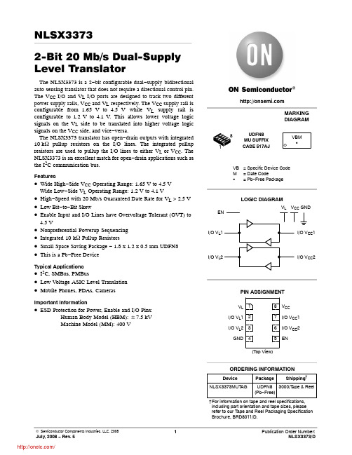
NLSX33732-Bit 20 Mb/s Dual-Supply Level TranslatorThe NLSX3373 is a 2−bit configurable dual−supply bidirectional auto sensing translator that does not require a directional control pin. The V CC I/O and V L I/O ports are designed to track two different power supply rails, V CC and V L respectively. The V CC supply rail isconfigurable from 1.65 V to 4.5 V while V L supply rail is configurable to 1.2 V to 4.1 V. This allows lower voltage logic signals on the V L side to be translated into higher voltage logic signals on the V CC side, and vice−versa.The NLSX3373 translator has open−drain outputs with integrated 10 k W pullup resistors on the I/O lines. The integrated pullup resistors are used to pullup the I/O lines to either V L or V CC. The NLSX3373 is an excellent match for open−drain applications such as the I2C communication bus.Features•Wide High−Side V CC Operating Range: 1.65 V to 4.5 VWide Low−Side V L Operating Range: 1.2 V to 4.1 V •High−Speed with 20 Mb/s Guaranteed Date Rate for V L > 2.5 V •Low Bit−to−Bit Skew•Enable Input and I/O Lines have Overvoltage Tolerant (OVT) to 4.5 V•Nonpreferential Powerup Sequencing•Integrated 10 k W Pullup Resistors•Small Space Saving Package − 1.8 x 1.2 x 0.5 mm UDFN8•This is a Pb−Free DeviceTypical Applications•I2C, SMBus, PMBus•Low V oltage ASIC Level Translation•Mobile Phones, PDAs, CamerasImportant Information•ESD Protection for Power, Enable and I/O Pins:Human Body Model (HBM): $7.5 kVMachine Model (MM): 400 VMARKINGDIAGRAMV L V CC GND I/O V L1I/O V L2CC1CC2LOGIC DIAGRAMUDFN8MU SUFFIXCASE 517AJVB= Specific Device CodeM= Date CodeG= Pb−Free PackageVBMGDevice Package Shipping†ORDERING INFORMATIONNLSX3373MUT AG UDFN8(Pb−Free)3000/T ape & ReelPIN ASSIGNMENT(T op View)V CCI/O V CC1I/O V CC2ENV LI/O V L1I/O V L2GND†For information on tape and reel specifications, including part orientation and tape sizes, please refer to our T ape and Reel Packaging Specification Brochure, BRD8011/D.87651234Figure 1. Block Diagram (1 I/O Line)R I/O V LI/O V CCWPIN ASSIGNMENTPins DescriptionV CC V CC Input Voltage V L V L Input Voltage GND Ground EN Output EnableI/O V CC n V CC I/O Port, Referenced to V CC I/O V L nV L I/O Port, Referenced to V LFUNCTION TABLEEN Operating ModeL Hi −ZHI/O Buses ConnectedMAXIMUM RATINGSSymbol Parameter Value Condition Unit V CC High−side DC Supply Voltage−0.3 to +7.0VV L High−side DC Supply Voltage−0.3 to +7.0VI/O V CC V CC−Referenced DC Input/Output Voltage−0.3 to (V CC + 0.3)VI/O V L V L−Referenced DC Input/Output Voltage−0.3 to (V L + 0.3)VV EN Enable Control Pin DC Input Voltage−0.3 to +7.0VI I/O_SC Short−Circuit Duration (I/O V L and I/O V CC to GND)40Continuous mA T STG Storage T emperature−65 to +150°C Stresses exceeding Maximum Ratings may damage the device. Maximum Ratings are stress ratings only. Functional operation above the Recommended Operating Conditions is not implied. Extended exposure to stresses above the Recommended Operating Conditions may affect device reliability.RECOMMENDED OPERATING CONDITIONSSymbol Parameter Min Max Unit V CC High−side Positive DC Supply Voltage 1.65 4.5V V L High−side Positive DC Supply Voltage 1.2 4.1V V EN Enable Control Pin Voltage GND 4.5V V IO Enable Control Pin Voltage GND 4.5V T A Operating T emperature Range−40+85°CDC ELECTRICAL CHARACTERISTICS (V CC = 1.65 V to 4.5 V and V L = 1.2 V to 4.1 V, unless otherwise specified)Symbol Parameter Test Conditions−405C to +855CUnit MinTyp(Notes 1, 2)MaxV IHC I/O V CC Input HIGH Voltage V CC− 0.4−−V V ILC I/O V CC Input LOW Voltage−−0.15V V IHL I/O V L Input HIGH Voltage V L− 0.2−−V V ILL I/O V L Input LOW Voltage−−0.15V V IH Control Pin Input HIGH Voltage V L− 0.2−−V V IL Control Pin Input LOW Voltage−−0.15V V OHC I/O V CC Output HIGH Voltage I/O V CC Source Current = 20 m A2/3 * V CC−−V V OLC I/O V CC Output LOW Voltage I/O V CC Sink Current = 20 m A−−1/3 * V CC V V OHL I/O V L Output HIGH Voltage I/O V L Source Current = 20 m A2/3 * V L−−V V OLL I/O V L Output LOW Voltage I/O V L Sink Current = 20 m A−−1/3 * V L V I QVCC V CC Supply Current I/O V CC and I/O V L Unconnected,V EN = V L−4575m AI QVL V L Supply Current I/O V CC and I/O V L Unconnected,V EN = V L− 1.0 5.0m AI TS−VCC V CC Tristate Output Mode Supply Current I/O V CC and I/O V L Unconnected,V EN = GND−0.1 2.5m AI TS−VL V L Tristate Output Mode Supply Current I/O V CC and I/O V L Unconnected,V EN = GND−0.1 2.5m AI OZ I/O Tristate Output Mode Leakage Current T A = +25°C−− 2.5m AR PU Pullup Resistor I/O V L and V CC T A = +25°C−10−k W1.Typical values are for V CC = +2.8 V, V L = +1.8 V and T A = +25°C.2.All units are production tested at T A = +25°C. Limits over the operating temperature range are guaranteed by design.Symbol Parameter Test Conditions−405C to +855C(Notes 3 and 4)Unit Min Typ Max+1.2 v V L v V CC v +4.5 Vt RVCC I/O V CC Risetime25ns t FVCC I/O V CC Falltime37ns t RVL I/O V L Risetime30ns t FVL I/O V L Falltime30ns t PDVL−VCC Propagation Delay (Driving I/O V L)30ns t PDVCC−VL Propagation Delay (Driving I/O V CC)30ns t PPSKEW Part−to−Part Skew20nS Maximum Data Rate8Mb/s +1.2 v V L v V CC v +3.3 Vt RVCC I/O V CC Risetime25ns t FVCC I/O V CC Falltime30ns t RVL I/O V L Risetime30ns t FVL I/O V L Falltime30ns t PDVL−VCC Propagation Delay (Driving I/O V L)20ns t PDVCC−VL Propagation Delay (Driving I/O V CC)20ns t PPSKEW Part−to−Part Skew10nS Maximum Data Rate10Mb/s +1.8 v V L v V CC v +2.5 Vt RVCC I/O V CC Risetime15ns t FVCC I/O V CC Falltime15ns t RVL I/O V L Risetime15ns t FVL I/O V L Falltime15ns t PDVL−VCC Propagation Delay (Driving I/O V L)15ns t PDVCC−VL Propagation Delay (Driving I/O V CC)15ns t PPSKEW Part−to−Part Skew10nS Maximum Data Rate16Mb/s +2.5 v V L v V CC v +3.3 Vt RVCC I/O V CC Risetime15ns t FVCC I/O V CC Falltime15ns t RVL I/O V L Risetime15ns t FVL I/O V L Falltime15ns t PDVL−VCC Propagation Delay (Driving I/O V L)15ns t PDVCC−VL Propagation Delay (Driving I/O V CC)15ns t PPSKEW Part−to−Part Skew10nS Maximum Data Rate20Mb/s3.Typical values are for V CC = +3.3 V, V L = +1.8 V and T A = +25°C.4.All units are production tested at T A = +25°C. Limits over the operating temperature range are guaranteed by design.Symbol Parameter Test Conditions−405C to +855C(Notes 5 and 6)Unit Min Typ Max+1.2 v V L v V CC v +4.5 Vt RVCC I/O V CC Risetime400ns t FVCC I/O V CC Falltime50ns t RVL I/O V L Risetime400ns t FVL I/O V L Falltime60ns t PDVL−VCC Propagation Delay (Driving I/O V L)1000ns t PDVCC−VL Propagation Delay (Driving I/O V CC)1000ns t PPSKEW Part−to−Part Skew50nS MDR Maximum Data Rate2Mb/s5.Typical values are for V CC = +3.3 V, V L = +1.8 V and T A = +25°C.6.All units are production tested at T A = +25°C. Limits over the operating temperature range are guaranteed by design. Limits over the operatingtemperature range are guaranteed by design.TEST SETUPSFigure 2. Rail −to −Rail Driving I/O V L I/O V CC CC C SourceCCFigure 3. Rail −to −Rail Driving I/O V CCFigure 4. Open −Drain Driving I/O V L I/O V CC CCFigure 5. Open −Drain Driving I/O V CCFigure 6. Definition of Timing Specification ParametersLOADV CCCOPENV 2xV CC TestSwitch t PZH , t PHZ Open t PZL , t PLZ2 x V CCC L = 15 pF or equivalent (Includes jig and probe capacitance)R L = R 1 = 50 k W or equivalentR T = Z OUT of pulse generator (typically 50 W )Figure 7. Test Circuit for Enable/Disable Time MeasurementV CC GNDGND HIGHIMPEDANCEV OL V OHHIGHIMPEDANCEFigure 8. Timing Definitions for Propagation Delays and Enable/Disable MeasurementENInputV L OutputOutputOutputAPPLICATIONS INFORMATIONLevel Translator ArchitectureThe NLSX3373 auto sense translator provides bi−directional voltage level shifting to transfer data in multiple supply voltage systems. This device has two supply voltages, V L and V CC, which set the logic levels on the input and output sides of the translator. When used to transfer data from the V L to the V CC ports, input signals referenced to the V L supply are translated to output signals with a logic level matched to V CC. In a similar manner, the V CC to V L translation shifts input signals with a logic level compatible to V CC to an output signal matched to V L. The NLSX3373 consists of two bi−directional channels that independently determine the direction of the data flow without requiring a directional pin. The one−shot circuits are used to detect the rising or falling input signals. In addition, the one shots decrease the rise and fall time of the output signal for high−to−low and low−to−high transitions. Each input/output channel has an internal 10 k W pull. The magnitude of the pullup resistors can be reduced by connecting external resistors in parallel to the internal 10 k W resistors.Input Driver RequirementsThe rise (t R) and fall (t F) timing parameters of the open drain outputs depend on the magnitude of the pull−up resistors. In addition, the propagation times (t PD), skew (t PSKEW) and maximum data rate depend on the impedance of the device that is connected to the translator. The timing parameters listed in the data sheet assume that the output impedance of the drivers connected to the translator is less than 50 k W.Enable Input (EN)The NLSX3373 has an Enable pin (EN) that provides tri−state operation at the I/O pins. Driving the Enable pin to a low logic level minimizes the power consumption of the device and drives the I/O V CC and I/O V L pins to a high impedance state. Normal translation operation occurs when the EN pin is equal to a logic high signal. The EN pin is referenced to the V L supply and has Overvoltage Tolerant (OVT) protection.Power Supply GuidelinesDuring normal operation, supply voltage V L should be less than or equal to V CC. The sequencing of the power supplies will not damage the device during the power up operation.The enable pin should be used to enter the low current tri−state mode, rather than setting either the V L or V CC supplies to 0 V. The NLSX3373 will not be damaged if either V L or V CC is equal to 0 V while the other supply voltage is at a nominal operating value; however, the operation of the translator cannot be guaranteed during single supply operation.For optimal performance, 0.01 m F to 0.1 m F decoupling capacitors should be used on the V L and V CC power supply pins. Ceramic capacitors are a good design choice to filter and bypass any noise signals on the voltage lines to the ground plane of the PCB. The noise immunity will be maximized by placing the capacitors as close as possible to the supply and ground pins, along with minimizing the PCB connection traces.PACKAGE DIMENSIONSUDFN8 1.8 x 1.2, 0.4P CASE 517AJ −01ISSUE ONOTES:1.DIMENSIONING AND TOLERANCING PER ASME Y14.5M, 1994.2.CONTROLLING DIMENSION: MILLIMETERS.3.DIMENSION b APPLIES TO PLATEDTERMINAL AND IS MEASURED BETWEEN 0.15 AND 0.30 mm FROM TERMINAL TIP .4.MOLD FLASH ALLOWED ON TERMINALS ALONG EDGE OF PACKAGE. FLASH MAY NOT EXCEED 0.03 ONTO BOTTOM SURFACE OF TERMINALS.5.DETAIL A SHOWS OPTIONALCONSTRUCTION FOR TERMINALS.DIM MIN MAX MILLIMETERS A 0.450.55A10.000.05A30.127 REF b 0.150.25D 1.80 BSC E 1.20 BSC e 0.40 BSC L 0.450.55b20.30 REF L10.000.03L20.40 REFNOTE 5L1DETAIL A0.328XDIMENSIONS: MILLIMETERSMOUNTING FOOTPRINT 7XSOLDERMASK DEFINEDON Semiconductor and are registered trademarks of Semiconductor Components Industries, LLC (SCILLC). SCILLC reserves the right to make changes without further notice to any products herein. SCILLC makes no warranty, representation or guarantee regarding the suitability of its products for any particular purpose, nor does SCILLC assume any liability arising out of the application or use of any product or circuit, and specifically disclaims any and all liability, including without limitation special, consequential or incidental damages. “Typical” parameters which may be provided in SCILLC data sheets and/or specifications can and do vary in different applications and actual performance may vary over time. All operating parameters, including “Typicals” must be validated for each customer application by customer’s technical experts. SCILLC does not convey any license under its patent rights nor the rights of others. SCILLC products are not designed, intended, or authorized for use as components in systems intended for surgical implant into the body,or other applications intended to support or sustain life, or for any other application in which the failure of the SCILLC product could create a situation where personal injury or death may occur. Should Buyer purchase or use SCILLC products for any such unintended or unauthorized application, Buyer shall indemnify and hold SCILLC and its officers, employees,subsidiaries, affiliates, and distributors harmless against all claims, costs, damages, and expenses, and reasonable attorney fees arising out of, directly or indirectly, any claim of personal injury or death associated with such unintended or unauthorized use, even if such claim alleges that SCILLC was negligent regarding the design or manufacture of the part.SCILLC is an Equal Opportunity/Affirmative Action Employer. This literature is subject to all applicable copyright laws and is not for resale in any manner.PUBLICATION ORDERING INFORMATION分销商库存信息: ONSEMINLSX3373MUTAG。
OP580;中文规格书,Datasheet资料
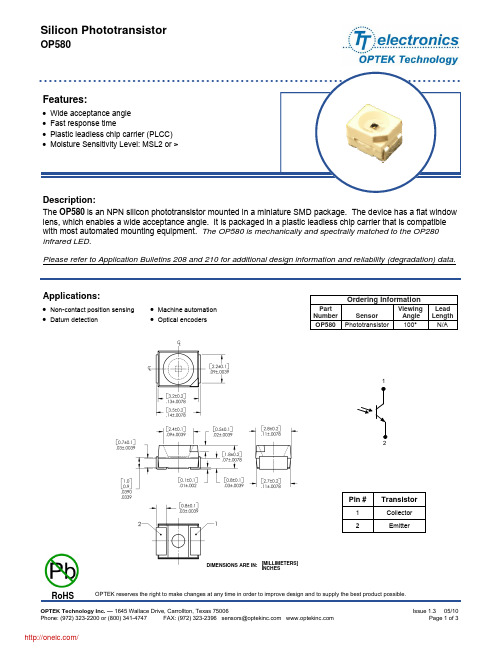
Silicon PhototransistorOP580Pin # Transistor1 Collector2 EmitterDescription:The OP580 is an NPN silicon phototransistor mounted in a miniature SMD package. The device has a flat window lens, which enables a wide acceptance angle. It is packaged in a plastic leadless chip carrier that is compatible with most automated mounting equipment. The OP580 is mechanically and spectrally matched to the OP280 infrared LED.Please refer to Application Bulletins 208 and 210 for additional design information and reliability (degradation) data.Ordering InformationPart Number Sensor Viewing Angle Lead LengthOP580 Phototransistor 100°N/AApplications:• Non-contact position sensing•Datum detection1• Machine automation • Optical encodersINCHES[MILLIMETERS]DIMENSIONS ARE IN:Silicon PhototransistorOP580Absolute Maximum Ratings (T A =25°C unless otherwise noted)Storage Temperature Range -40o C to +85o C Operating Temperature Range -25o C to +85o CLead Soldering Temperature 260° C (1)Collector-Emitter Voltage 30 V Collector Current 20 mA Power Dissipation75 mW (2)Emitter-Collector Voltage 5 V Notes:1. Solder time less than 5 seconds at temperature extreme.2. Derate linearly at 2.17 mW/° C above 25° C.3. E E(APT) is an unfiltered GaAs LED with a peak emission wavelength of 935 nm and a radiometric intensity level which varies less than10% over the entire lens surface of the phototransistor being tested.4. To calculate typical collector dark current in µA, use the formula I CEO = 10(0.04 Ta-3.4) where T a is the ambient temperature in ° C.Electrical Characteristics (T A = 25°C unless otherwise noted)SYMBOL PARAMETER MIN TYP MAX UNITS TEST CONDITIONS I C(ON)On-State Collector Current1.0 - - mA V CE = 5.0 V, E E = 5.0 mW/cm 2(3) V CE(SAT) Collector-Emitter Saturation Voltage - - 0.4 V I C = 100 µA, E E =2.0 mW/cm 2(3) I CE0Collector-Emitter Dark Current- - 100 nAV CE = 5.0 V, E E = 0(4)V (BR)CEOCollector-EmitterBreakdown Voltage 30 - - V I C = 100 µA V (BR)ECO Emitter-Collector Breakdown Voltage 5 - - V I E = 100 µA t r , t fRise Time , Fall Time-15-µsI C = 1 mA, R L = 1 K ΩR e l a t i v e R e s p o n s e (%)R e l a t i v e R e s p o n s e (%)Angular Position (Degrees)Relative Response vs Angular Position-90 30 600 -30 -60 90Silicon PhototransistorOP580Relative On-State Collector Current vsIrradianceEE rradiance (mW/cm 2)R e l a t i v e C o l l e c t o r C u r r e n t (%)0 1 2 3 4 5 6 7 8R e l a t i v e C o l l e ct o r C u r r e n t (%)Relative On-State Collector Current vsI C (O N ) - O n -S t a t e C o l l e c t o r C u r r e n t (m A )Relative On-State Collector Current vsCollector-Emitter VoltageCollector-Emitter Voltage (V)0 0.1 0.2 0.3 0.4 0.5Collector-Emitter Dark Current vsTemperatureTemperature (°C)C o l l e c t o r -E m i t t e rD a rk C u r r e n t (n A )-250 25 50 75 100分销商库存信息: OPTEK-TECHNOLOGY OP580。
RO3075A;中文规格书,Datasheet资料
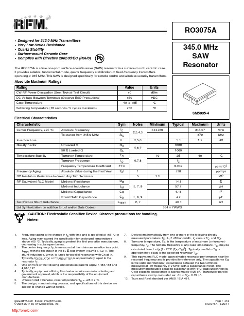
Electrical Characteristics CharacteristicSymNotesMinimumTypical MaximumUnitsCenter Frequency, +25 °C Absolute Frequency f C 2,3,4,5344.930345.07MHz Tolerance from 345.0 MHz∆f C ±70kHz Insertion Loss IL 2,5,6 1.3 1.7dBQuality Factor Unloaded Q Q U 5,6,7800050 Ω Loaded Q Q L 1000Temperature StabilityTurnover Temperature T O 6,7,8102540°C Turnover Frequencyf O f C Frequency Temperature CoefficientFTC 0.032ppm/°C 2Frequency AgingAbsolute Value during the First Year |f A |1≤10ppm/yr DC Insulation Resistance between Any Two Terminals51.0M ΩRF Equivalent RLC ModelMotional Resistance R M 5, 7, 914.1ΩMotional Inductance L M 57.7µH Motional Capacitance C M 4.11fF Shunt Static CapacitanceC O 5, 6, 9 4.2pF Test Fixture Shunt InductanceL TEST2, 749.8nHLid Symbolization (in addition to Lot and/or Date Codes)664 // YWWS•Designed for 345.0MHz Transmitters •Very Low Series Resistance •Quartz Stability•Surface-mount Ceramic Case•Complies with Directive 2002/95/EC (RoHS)The RO3075A is a true one-port, surface-acoustic-wave (SAW) resonator in a surface-mount, ceramic case. It provides reliable, fundamental-mode, quartz frequency stabilization of fixed-frequency transmittersoperating at 345MHz. This SAW is designed specifically for remote control and wireless security transmitters.Absolute Maximum Ratings RatingValueUnitsCW RF Power Dissipation (See: Typical Test Circuit)+0dBm DC Voltage Between Terminals (Observe ESD Precautions)±30VDC Case Temperature-40 to +85°C Soldering Temperature (10 seconds / 5 cycles maximum)260°C345.0 MHz SAW ResonatorRO3075ACAUTION: Electrostatic Sensitive Device. Observe precautions for handling.Notes:1.Frequency aging is the change in f C with time and is specified at +65 °C or less. Aging may exceed the specification for prolonged temperaturesabove +65 °C. Typically, aging is greatest the first year after manufacture, decreasing in subsequent years.2.The center frequency, f C , is measured at the minimum insertion loss point, IL MIN , with the resonator in the 50Ω test system (VSWR ≤ 1.2:1). The shunt inductance, L TEST , is tuned for parallel resonance with C O at f C . Typically, f OSCILLATOR or f TRANSMITTER is approximately equal to the resonator f C .3.One or more of the following United States patents apply: 4,454,488 and 4,616,197.4.Typically, equipment utilizing this device requires emissions testing and government approval, which is the responsibility of the equipment manufacturer.5.Unless noted otherwise, case temperature T C =+25±2°C.6.The design, manufacturing process, and specifications of this device are subject to change without notice.7.Derived mathematically from one or more of the following directly measured parameters: f C , IL, 3dB bandwidth, f C versus T C , and C O .8.Turnover temperature, T O , is the temperature of maximum (or turnover) frequency, f O . The nominal frequency at any case temperature, T C , may be calculated from: f =f O [1-FTC (T O -T C )2]. Typically oscillator T O is approximately equal to the specified resonator T O .9.This equivalent RLC model approximates resonator performance near the resonant frequency and is provided for reference only. The capacitance C O is the static (nonmotional) capacitance between the two terminals measured at low frequency (10MHz) with a capacitance meter. Themeasurement includes parasitic capacitance with "NC” pads unconnected. Case parasitic capacitance is approximately 0.05pF. Transducer parallel capacitance can by calculated as: C P ≈C O -0.05pF.10.Tape and Reel standard per ANSI / EIA 481.PbElectrical ConnectionsThe SAW resonator is bidirectional and may beinstalled with either orientation. The two terminalsare interchangeable and unnumbered. The calloutNC indicates no internal connection. The NC padsassist with mechanical positioning and stability.External grounding of the NC pads isrecommended to help reduce parasiticcapacitance in the circuit.Typical Test CircuitThe test circuit inductor, L TEST, is tuned to resonate with the static capacitance, C O, at F C.Typical Application Circuits Equivalent Model Temperature Characteristics The curve shown on the right accounts for resonator contribution only and does not include LC component temperature contributions.CaseDimensionsMillimeters InchesMin Nom Max Min Nom MaxA 4.87 5.00 5.130.1910.1960.201B 3.37 3.50 3.630.1320.1370.142C 1.45 1.53 1.600.0570.0600.062D 1.35 1.43 1.500.0400.0570.059E0.670.800.930.0260.0310.036 F0.370.500.630.0140.0190.024G 1.07 1.20 1.330.0420.0470.052H- 1.04--0.041-I- 1.46--0.058-J-0.50--0.019-K- 1.05--0.041-L- 1.44--0.057-M-0.71--0.028-PCB Land PatternTop View分销商库存信息: RFMRO3075A。
AM2520SRC03;中文规格书,Datasheet资料

Notes: 1.Wavelength: +/-1nm. 2. Forward Voltage: +/-0.1V.
Absolute Maximum Ratings at TA=25°C
Parameter Power dissipation DC Forward Current Peak Forward Current [1] Reverse Voltage Operating Temperature Storage Temperature
DATE: APR/14/2011 DRAWN: J.Yu
PAGE: 5 OF 5 ERP: 1202000669
/
分销商库存信息:
KINGBRIGHT AM2520SRC03
Part No. Dice Lens Type Iv (mcd) [2] @ 20mA Min. AM2520SRC03 Super Bright Red (GaAlAs) Water Clear 600 Typ. 800 Viewing Angle [1] 2θ1/2 20°
Notes: 1. θ1/2 is the angle from optical centerline where the luminous intensity is 1/2 of the optical peak value. 2. Luminous intensity/ luminous Flux: +/-15%.
SPEC NO: DSAA4194 APPROVED: WYNEC
REV NO: V.8 CHECKED: Allen Liu
DATE: APR/14/2011 DRAWN: J.Yu
PAGE: 1 OF 5 ERP: 1202000669
RTQ035N03TR;中文规格书,Datasheet资料

Appendix1-Rev1.1
/
分销商库存信息:
ROHM RTQ035N03TR
2.9 1.9 0.95 0.95
(6) (5) (4)
1.6 2.8
0~0.1
(3)
1/2
/
RTQ035N03
Transistors
zElectrical characteristics (Ta=25°C)
Parameter Symbol IGSS Gate-source leakage Drain-source breakdown voltage V(BR) DSS IDSS Zero gate voltage drain current VGS (th) Gate threshold voltage
The products listed in this document are designed to be used with ordinary electronic equipment or devices (such as audio visual equipment, office-automation equipment, communications devices, electrical appliances and electronic toys). Should you intend to use these products with equipment or devices which require an extremely high level of reliability and the malfunction of with would directly endanger human life (such as medical instruments, transportation equipment, aerospace machinery, nuclear-reactor controllers, fuel controllers and other safety devices), please be sure to consult with our sales representative in advance. About Export Control Order in Japan Products described herein are the objects of controlled goods in Annex 1 (Item 16) of Export Trade Control Order in Japan. In case of export from Japan, please confirm if it applies to "objective" criteria or an "informed" (by MITI clause) on the basis of "catch all controls for Non-Proliferation of Weapons of Mass Destruction.
cisco3550配置手册
产品特性3550EMI是支持二层、三层功能(EMI)的交换机支持VLAN〃 到1005 个VLAN〃 支持VLAN ID从1到4094(IEEE 802.1Q 标准)〃 支持ISL及IEEE 802.1Q封装安全〃 支持IOS标准的密码保护〃 静态MAC地址映射〃 标准及扩展的访问列表支持,对于路由端口支持入出双向的访问列表,对于二层端口支持入的访问列表〃 支持基于VLAN的访问列表3层支持(需要多层交换的IOS)〃 HSRP〃 IP路由协议o RIP versions 1 and 2o OSPFo IGRP及EIGRPo BGP Version 4监视〃 交换机LED指示端口状态〃 SPAN及远端SPAN (RSPAN) 可以监视任何端口或VLAN的流量〃 内置支持四组的RMON监控功能(历史、统计、告警及事件)〃 Syslog功能其它功能:支持以下的GBIC模块:〃 1000BASE-T GBIC: 铜线最长100 m〃 1000BASE-SX GBIC: 光纤最长1804 feet (550 m)〃 1000B ASE-LX/LH GBIC: 光纤最长32,808 feet (6 miles or 10 km) 〃 1000BASE-ZX GBIC: 光纤最长328,084 feet (62 miles or 100 km) 配置端口配置一组端口命令目的Step 1 configure terminal 进入配置状态Step 2 interface range {port-range} 进入组配置状态Step 3 可以使用平时的端口配置命令进行配置Step 4 end 退回Step 5 show interfaces [interface-id] 验证配置Step 6 copy running-config startup-config 保存当使用interface range命令时有如下的规则:〃 有效的组范围:o vlan从1 到4094o fastethernet 槽位/{first port} - {last port}, 槽位为0o gigabitethernet槽位/{first port} - {last port},槽位为0o port-channel port-channel-number - port-channel-number, port-channel号从1到64〃 端口号之间需要加入空格,如:interface range fastethernet 0/1 – 5 是有效的,而interface range fastethernet 0/1-5 是无效的.〃 interface range 命令只能配置已经存在的interface vlan〃 所有在同一组的端口必须是相同类别的。
STPS30100ST;中文规格书,Datasheet资料
October 2006 Rev 11/7STPS30100STPower Schottky rectifierMain product characteristicsFeatures and Benefits■Avalanche rated ■Low V F■Good trade off between leakage current and forward voltage drop ■High frequency operation ■Avalanche capability specifiedDescriptionSingle Schottky rectifier, suited for high frequency switch mode power supply.Packaged in TO-220AB, this device is intended to be used in notebook and game station adaptors, providing in these applications a good efficiency at both low and high load.I F(AV)30 A V RRM 100 V T j (max)150° C V F (typ)0.385 VTable 1.Absolute Ratings (limiting values)Symbol ParameterValue Unit V RRM Repetitive peak reverse voltage 100V I F(RMS)RMS forward current60A I F(AV)Average forward current δ = 0.5T c = 125° C 30A I FSM Surge non repetitive forward current t p = 10 ms sinusoidal 300A P ARM Repetitive peak avalanche power t p = 1 µs T j = 25° C26400W T stg Storage temperature range-65 to + 175°C T jMaximum operating junction temperature (1)1. condition to avoid thermal runaway for a diode on its own heatsink150°CdPtot dTj---------------1Rth j a –()-------------------------<Characteristics STPS30100ST2/71 CharacteristicsTo evaluate the conduction losses use the following equation:P = 0.475 x I F(AV) + 0.006 x I F 2(RMS)Table 2.Thermal resistanceSymbol ParameterValue Unit R th(j-c)Junction to case1°C/WTable 3.Static electrical characteristics (per diode)SymbolParameterTest Conditions Min.Typ.Max.Unit I R (1)1.Pulse test: t p = 5 ms, δ < 2%Reverse leakage currentT j = 25° CV R = V RRM175µA T j = 125° C 2050mA T j = 25° C V R = 70 V 60µA T j = 125° C 1020mAV F (2)2.Pulse test: t p = 380 µs, δ < 2%Forward voltage dropT j = 25° C I F = 5 A0.475VT j = 125° C 0.385T j = 25° C I F = 10 A0.555T j = 125° C 0.475T j = 25° C I F = 15 A 0.6200.660T j = 125° C 0.5250.565T j = 25° C I F = 30 A0.7400.800T j = 125° C0.6050.655STPS30100STCharacteristics3/7Figure 1.Conduction losses versus average Figure 2.Average forward current versusTδ=t /Tp tTδ=t p /Tt Figure 3.Normalized avalanche power derating versus pulse durationFigure 4.Normalized avalanche power derating versus junction Figure 5.Non repetitive surge peak forward current versus overload duration Figure 6.Relative variation of thermalimpedance junction to case versusCharacteristicsSTPS30100ST4/7Figure 7.Reverse leakage current versusreverse voltage applied (typicalFigure 8.Junction capacitance versus reverse voltage applied (typical Figure 9.Forward voltage drop versusFigure 10.Forward voltage drop versusSTPS30100ST Package Information5/72 Package InformationEpoxy meets UL94,V0In order to meet environmental requirements, ST offers these devices in ECOP ACK®packages. These packages have a lead-free second level interconnect. The category of second level interconnect is marked on the package and on the inner box label, in compliance with JEDEC Standard JESD97. The maximum ratings related to soldering conditions are also marked on the inner box label. ECOP ACK is an ST trademark. ECOP ACK specifications are available at: .Ordering Information STPS30100ST6/73 Ordering Information4 Revision HistoryOrdering type Marking Package Weight Base qtyDelivery modeSTPS30100STSTPS30100STTO-220AB2.23 g50TubeDate RevisionChanges24-Oct-20061First issueSTPS30100STPlease Read Carefully:Information in this document is provided solely in connection with ST products. STMicroelectronics NV and its subsidiaries (“ST”) reserve the right to make changes, corrections, modifications or improvements, to this document, and the products and services described herein at any time, without notice.All ST products are sold pursuant to ST’s terms and conditions of sale.Purchasers are solely responsible for the choice, selection and use of the ST products and services described herein, and ST assumes no liability whatsoever relating to the choice, selection or use of the ST products and services described herein.No license, express or implied, by estoppel or otherwise, to any intellectual property rights is granted under this document. If any part of this document refers to any third party products or services it shall not be deemed a license grant by ST for the use of such third party products or services, or any intellectual property contained therein or considered as a warranty covering the use in any manner whatsoever of such third party products or services or any intellectual property contained therein.UNLESS OTHERWISE SET FORTH IN ST’S TERMS AND CONDITIONS OF SALE ST DISCLAIMS ANY EXPRESS OR IMPLIED WARRANTY WITH RESPECT TO THE USE AND/OR SALE OF ST PRODUCTS INCLUDING WITHOUT LIMITATION IMPLIED WARRANTIES OF MERCHANTABILITY, FITNESS FOR A PARTICULAR PURPOSE (AND THEIR EQUIVALENTS UNDER THE LAWS OF ANY JURISDICTION), OR INFRINGEMENT OF ANY PATENT, COPYRIGHT OR OTHER INTELLECTUAL PROPERTY RIGHT. UNLESS EXPRESSLY APPROVED IN WRITING BY AN AUTHORIZED ST REPRESENTATIVE, ST PRODUCTS ARE NOT RECOMMENDED, AUTHORIZED OR WARRANTED FOR USE IN MILITARY, AIR CRAFT, SPACE, LIFE SAVING, OR LIFE SUSTAINING APPLICATIONS, NOR IN PRODUCTS OR SYSTEMS WHERE FAILURE OR MALFUNCTION MAY RESULT IN PERSONAL INJURY, DEATH, OR SEVERE PROPERTY OR ENVIRONMENTAL DAMAGE. ST PRODUCTS WHICH ARE NOT SPECIFIED AS "AUTOMOTIVE GRADE" MAY ONLY BE USED IN AUTOMOTIVE APPLICATIONS AT USER’S OWN RISK.Resale of ST products with provisions different from the statements and/or technical features set forth in this document shall immediately void any warranty granted by ST for the ST product or service described herein and shall not create or extend in any manner whatsoever, any liability of ST.ST and the ST logo are trademarks or registered trademarks of ST in various countries.Information in this document supersedes and replaces all information previously supplied.The ST logo is a registered trademark of STMicroelectronics. All other names are the property of their respective owners.© 2006 STMicroelectronics - All rights reservedSTMicroelectronics group of companiesAustralia - Belgium - Brazil - Canada - China - Czech Republic - Finland - France - Germany - Hong Kong - India - Israel - Italy - Japan - Malaysia - Malta - Morocco - Singapore - Spain - Sweden - Switzerland - United Kingdom - United States of America7/7分销商库存信息: STMSTPS30100ST。
MBR0530;中文规格书,Datasheet资料

Thermal Characteristics
Symbol
Parameter
RθJA RθJL
Thermal Resistance, Junction to Ambient * Thermal Resistance, Junction to Lead
* 1 inch square pad size on FR-4 board.
¥
Saving our world, 1mW/W/kW at a time™ SignalWise¥ SmartMax¥ SMART START¥ Solutions for Your Success¥ SPM® STEALTH¥ SuperFET® SuperSOT¥-3 SuperSOT¥-6 SuperSOT¥-8 SupreMOS® SyncFET¥ Sync-Lock™
ANTI-COUNTERFEITING POLICY
Fairchild Semiconductor Corporation's Anti-Counterfeiting Policy. Fairchild's Anti-Counterfeiting Policy is also stated on our external website, , under Sales Support.
March 2012
SOD123 Color Band Denotes Cathode
Mark: B3
Absolute Maximum Ratings *
Values are at TA=25°C unless otherwise noted.
Symbol
Parameter
Value
Unit
VRRM Maximum Repetitive Reverse Voltage
RFC3550中文版
RFC3550RTP:实时应用程序传输协议摘要本文描述RTP(real-time transport protocol),实时传输协议。
RTP在多点传送(多播)或单点传送(单播)的网络服务上,提供端对端的网络传输功能,适合应用程序传输实时数据,如:音频,视频或者仿真数据。
RTP没有为实时服务提供资源预留的功能,也不能保证QoS(服务质量)。
数据传输功能由一个控制协议(RTCP)来扩展,通过扩展,可以用一种方式对数据传输进行监测控制,该协议(RTCP)可以升级到大型的多点传送(多播)网络,并提供最小限度的控制和鉴别功能。
RTP和RTCP被设计成和下面的传输层和网络层无关。
协议支持RTP标准的转换器和混合器的使用。
本文的大多数内容和旧版的RFC1889相同。
在线路里传输的数据包格式没有改变,唯一的改变是使用协议的规则和控制算法。
为了最小化传输,发送RTCP数据包时超过了设定的速率,而在这时,很多的参与者同时加入了一个会话,在这样的情况下,一个新加入到(用于计算的可升级的)计时器算法中的元素是最大的改变。
目录(Table of Contents)1. 引言(Introduction)1 1 术语(Terminology)2 RTP使用场景(RTP Use Scenarios)2 1 简单多播音频会议( Simple Multicast Audio Conference)2 2 音频和视频会议(Audio and Video Conference)2 3 混频器和转换器(Mixers and Translators)2 4 分层编码(Layered Encodings)3 定义(Definitions)4 字节序,校正和时间格式(Byte Order, Alignment, and Time Format)5 RTP数据传输协议(RTP Data Transfer Protocol)5 1 RTP固定头域(RTP Fixed Header Fields)5 2 多路复用RTP会话(Multiplexing RTP Sessions)5 3 RTP头的配置文件详细变更(Profile-Specific Modifications to the RTP Header)5 3 1 RTP报头扩展(RTP Header Extension)6 RTP控制协议(RTP Control Protocol) -- RTCP6 1 RTCP包格式(RTCP Packet Format)6 2 RTCP传输间隔(RTCP Transmission Interval)6 2 1 维护会话成员数目(Maintaining the number of session members)6 3 RTCP包的发送与接收规则(RTCP Packet Send and Receive Rules)6 3 1 计算RTCP传输间隔(Computing the RTCP Transmission Interval)6 3 2 初始化(Initialization)6 3 3 接收RTP或RTCP(非BYE)包(Receiving an RTP or Non-BYE RTCP Packet)6 3 4 接收RTCP(BYE)包(Receiving an RTCP BYE Packet)6 3 5 SSRC计时失效(Timing Out an SSRC)6 3 6 关于传输计时器的到期(Expiration of Transmission Timer)6 37 传输一个 BYE 包(Transmitting a BYE Packet)6 3 8 更新we_sent(Updating we_sent)6 3 9 分配源描述带宽(Allocation of Source Description Bandwidth)6 4 发送方和接收方报告(Sender and Receiver Reports)6 4 1 SR:发送方报告的RTCP包(SR: Sender report RTCP packet)6 4 2 RR:接收方报告的RTCP包(RR: Receiver Report RTCP Packet)6 4 3 扩展发送方和接收方报告(Extending the Sender and Receiver Reports )6 4 4 分析发送方和接收方报告(Analyzing Sender and Receiver Reports )6 5 SDES:源描述RTCP包(SDES: Source description RTCP packet)6 5 1 CNAME:规范终端标识符的SDES数据项(CNAME: Canonical End-Point Identifier SDES Item)6 5 2 NAME:用户名的SDES数据项(NAME: User name SDES item)6 5 3 EMAIL:电子邮件地址的SDES数据项(EMAIL: Electronic Mail Address SDES Item) 6 5 4 PHONE:电话号码的SDES数据项(PHONE: Phone Number SDES Item)6 5 5 LOC:地理用户地址的SDES数据项(LOC: Geographic User Location SDES Item)6 5 6 TOOL:应用程序或工具名字的SDES数据项(TOOL: Application or Tool Name SDES Item) 6 57 NOTE:通知/状态的SDES数据项(NOTE: Notice/Status SDES Item)6 5 8 PRIV:私有扩展的SDES数据项(PRIV: Private Extensions SDES Item)6 6 BYE:Goodbye RTCP包(BYE: Goodbye RTCP packet)6 7 APP:定义应用程序的RTCP包(APP: Application-Defined RTCP Packet)7 RTP转换器和混频器(RTP Translators and Mixers)7 1 概述(General Description )7 2 在转换器中的RTCP数据处理(RTCP Processing in Translators)7 3 在混频器中的RTCP数据处理(RTCP Processing in Mixers )7 4 级联混频器(Cascaded Mixers)8 SSRC标识符的分配和使用(SSRC Identifier Allocation and Use)8 1 冲突概率(Probability of Collision )8 2 冲突解决和循环检测(Collision Resolution and Loop Detection)8 3 在分层编码中使用(Use with Layered Encodings)9 安全(Security )9 1 机密性(Confidentiality)9 2 身份验证和消息完整性(Authentication and Message Integrity)10 拥塞控制(Congestion Control)11 网络和传输协议之上的RTP(RTP over Network and Transport Protocols)12 协议常量摘要(Summary of Protocol Constants)12 1 RTCP 包类型(RTCP Packet Types)12 2 SDES 类型(SDES Types)13 RTP概况和负载格式详细说明(RTP Profiles and Payload Format Specifications)14 安全考虑(Security Considerations)15 IANA考虑(IANA Considerations)16 知识产权声明(Intellectual Property Rights Statement)17 鸣谢(Acknowledgments)附录 A 算法(Algorithms)附录 A 1 RTP数据头有效性检查(RTP Data Header Validity Checks )附录 A 2 RTCP数据头有效性检查(RTCP Header Validity Checks)附录 A 3 确定RTP包预期数目和丢失数目(Determining Number of Packets Expected and Lost)附录 A 4 生成SDES RTCP包(Generating RTCP SDES Packets)附录 A 5 解析RTCP SDES包(Parsing RTCP SDES Packets)附录 A 6 生成32位随机标识符(Generating a Random 32-bit Identifier附录 A 7 计算RTCP传输间隔(Computing the RTCP Transmission Interval)附录 A 8 估测两次到达间隔的抖动(Estimating the Interarrival Jitter)附录 B 与RFC1889不同之外(Changes from RFC 1889)参考书目(References)标准化引用(Normative References )资料性引用(Informative References)作者地址完整的版权声明1.绪论本文详细的介绍实时传输协议RTP,RTP提供带有实时特性的端对端数据传输服务,传输的数据如:交互式的音频和视频。
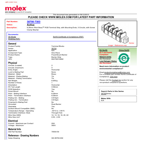
0387007303;中文规格书,Datasheet资料
This document was generated on 09/12/2012PLEASE CHECK FOR LATEST PART INFORMATIONPart Number:38700-7303Status:ActiveDescription:8.26mm Pitch Beau™ PCB Terminal Strip, with Mounting Ends, 3 Circuits, with Screw Clamp WasherDocuments:3D ModelRoHS Certificate of Compliance (PDF)Drawing (PDF)GeneralProduct Family Terminal Blocks Series38700ApplicationN/AComponent Type One PieceProduct Name Fixed Mount Barrier Type Barrier Strip UPC800756316802PhysicalCircuits (Loaded)3Circuits (maximum)3Entry AngleHorizontal Lock to Mating Part None Material - MetalBrass Material - Plating MatingTin Material - Plating Termination Tin Net Weight8.950/g Number of Rows 1Orientation Horizontal PC Tail Length 3.56mm PCB Retention Yes Panel MountNoPitch - Mating Interface8.26mm Pitch - Termination Interface 8.26mm Plating min - Mating3.810µm Plating min - Termination 3.810µm Polarized to Mating Part NoShrouded Dual-Barrier StackableYes Surface Mount Compatible (SMC)NoTemperature Range - Operating -40°C to +130°C Termination Interface: Style Through HoleWire Size AWG 12, 14, 16, 18, 20, 22Wire Size mm²0.50 - 2.50ElectricalCurrent - Maximum per Contact 20A Voltage - Maximum300V Material InfoOld Part Number70503-50Reference - Drawing NumbersSales DrawingSD-38700-002Seriesimage - Reference onlyEU RoHSChina RoHSELV and RoHS Compliant REACH SVHC Not ReviewedLow-Halogen Status Not ReviewedNeed more information on product environmental compliance?Email productcompliance@For a multiple part number RoHS Certificate of Compliance, click herePlease visit the Contact Us section for any non-product compliance questions.Search Parts in this Series 38700Series Mates With N/AThis document was generated on 09/12/2012PLEASE CHECK FOR LATEST PART INFORMATION分销商库存信息: MOLEX 0387007303。
AA3528QBSD, 规格书,Datasheet 资料
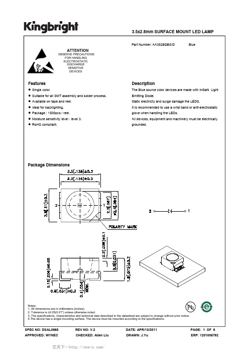
SPEC NO: DSAL0865 APPROVED: WYNEC
REV NO: V.2 CHECKED: Allen Liu
DATE: APR/13/2011 DRAWN: J.Yu
PAGE: 1 OF 6 ERP: 1201006792
芯天下--/
Handling Precautions
2. Do not directly touch or handle the silicone lens surface. It may damage the internal circuitry.
3. Do not stack together assembled PCBs containing exposed LEDs. Impact may scratch the silicone lens or damage the internal circuitry.
Electrical / Optical Characteristics at TA=25°C
Symbol λpeak λD [1] Δλ1/2 C VF [2] IR Parameter Peak Wavelength Dominant Wavelength Spectral Line Half-width Capacitance Forward Voltage Reverse Current Device Blue Blue Blue Blue Blue Blue Typ. 468 470 25 100 3.3 4 50 Max. Units nm nm nm pF V uA Test Conditions IF=20mA IF=20mA IF=20mA VF=0V;f=1MHz IF=20mA VR=5V
15-000803;中文规格书,Datasheet资料

05.10.09 15.04.09
HS HS
d-old
15K1A319
part no:
A3 sh: 2
A
APPROVAL # FREIGABE # DEBLOCAGE # AUTORIZACION # APPROVAL
rev. description
D
date
name
C
see sheet 1
/
A
scale: material: title: 3:1 see sheet 1
A
APPROVAL # FREIGABE # DEBLOCAGE # AUTORIZACION
APPROVAL # FREIGABE # DEBLOCAGE # AUTORIZACION # APPROVAL
CUSTOMER APPROVAL DATE:
0,3 78 + -0
c
0,02 8+ - 0,23
C
63,5 `0,13
0 54,96 + - 0,25
0,3 21,1 + -0
10°
PRESS FOR FIXING ON PCB
B
METAL BRACKET
3,2 `0,2 SEALING COMPOUND
B
O-RING
15-00080o CONEC ABC
DO NOT ALTER CAD DRAWING BY HAND
tolerance
dim. in mm
date
drawn appd. norm
APPROVAL # FREIGABE # DEBLOCAGE # AUTORIZACION
A
name
MBRA140T3G;MBRA140T3;中文规格书,Datasheet资料

Figure 5. Current Derating
R (T) , TRANSIENT THERMAL RESISTANCE (NORMALIZED) T, TIME (s) 1.0E+0
Figure 6. Forward Power Dissipation
中文规格书datasheet资料datasheetdatasheet网站l298ndatasheeticdatasheetpl2303datasheetds18b20datasheetdatasheetcomlm324datasheetrt5350datasheet
MBRA140T3G, NRVBA140T3G Surface Mount Schottky Power Rectifier
vF, INSTANTANEOUS FORWARD VOLTAGE (VOLTS)
Figure 1. Typical Forward Voltage
Figure 2. Maximum Forward Voltage
100E-3 I R , REVERSE CURRENT (AMPS)
100E-3 I R , MAXIMUM REVERSE CURRENT (AMPS)
†For information on tape and reel specifications, including part orientation and tape sizes, please refer to our Tape and Reel Packaging Specifications Brochure, BRD8011/D.
10E-3
TJ = 125C TJ = 85C
10E-3 TJ = 85C 1.0E-3 TJ = 25C
IOM HM0800 技术手册说明书

IOMHM0800技术手册目录1 概述 (1)1.1 简介 (1)1.2 特性 (1)2 输入/输出 (2)2.1 端子定义 (2)2.2 电源输入(L、、N) (3)2.3 通用输入(UI1~UI8) (3)2.4 通讯接口(RS485) (4)2.5 安装尺寸图 (4)2.6 安装指导 (5)2.7 面板按键 (5)2.7.1 EOL开关 (5)2.7.2 复位开关(RESET按键) (5)2.7.3 拨码开关 (6)3 规格和技术参数 (7)3.1 规格 (7)3.2 连接端子 (7)3.3 辅助工具 (8)3.4 环境条件和保护 (8)3.5 标准、指令和审核 (8)3.6 常规信息表 (9)3.7 通讯协议 (9)4 选型清单 (12)1 概述1.1 简介HM0800拓展模块用于拓展控制器的I/O点位,具备RS485通讯总线,支持ModBus RTU与BACnet MS/TP协议,推荐与海林HD系列DDC搭配使用,也可兼容第三方控制器或平台。
1.2 特性·支持交直流24V供电·支持ModBus RTU、BACnet MS/TP通讯协议·具备1路RS485通讯接口,波特率支持最大115200bps·具备实体终端电阻按钮(EOL),无需外置总线匹配电阻·具备通用输入接口·具备独立的配置软件,既可与HD系列DDC搭配使用,也可快速接入其他平台2 输入/输出2.1 端子定义2.2 电源输入(L、PE、N)支持AC/DC 24V(±10%)供电2.3 通用输入(UI1~UI8)具备8路UI输入,每路UI可支持0~10V模拟电压、4~20mA模拟电流、电阻类(NTC 10K、NTC 2.25K、PT1000、LG Ni 1000)和干接点通断共4类输入信号2.4 通讯接口(RS485)具备1路带隔离保护的RS485接口2.5 安装尺寸图2.6 安装指导步骤 1:将HM0800挂在导轨上,使产品底部的卡勾与导轨完全贴合;步骤 2:同时按压导轨与产品表面,听到“咔”一声,表示产品与导轨安装成功;板子上的MOS器件对静电敏感,需做好防护措施2.7 面板按键2.7.1 EOL开关EOL开关:按下时,RS485终端电阻(120Ω)接通,弹起时,终端电阻(120Ω)不接通。
