Design and Analysis of High-Power LED Car Headlamps Radiator
高功率密度激发荧光材料的反常热猝灭效应
1456㊀发㊀㊀光㊀㊀学㊀㊀报第42卷[8]HAGEMANN V,SEIDL A,WEIDMANN G.Ceramic phosphor wheels for high luminance SSL-light sources with>500Wof laser power for digital projection[C].Proceedings of SPIE10940,Light-Emitting Devices,Materials,and Applications, San Francisco,2019:1094017-1-16.[9]YANG Y,ZHUANG S L,KAI B.High brightness laser-driven white emitter for Etendue-limited applications[J].Appl.Opt.,2017,56(30):8321-8325.[10]金伟其,王霞,廖宁放,等.辐射度光度与色度及其测量[M].第2版.北京:北京理工大学出版社,2016.JIN W Q,WANG X,LIAO N F,et al.Photometry,Radiometry,Colorimetry&Measurement[M].2nd ed.Beijing:Beijing Institute of Technology Press,2016.(in Chinese)[11]ZHENG P,LI S X,WANG L,et al.Unique color converter architecture enabling phosphor-in-glass(PiG)films suitable forhigh-power and high-luminance laser-driven white lighting[J].ACS Appl.Mater.Interfaces,2018,10(17):14930-14940.㊀[12]WANG J C,TANG X Y,ZHENG P,et al.Thermally self-managing YAGʒCe-Al2O3color converters enabling high-bright-ness laser-driven solid state lighting in a transmissive configuration[J].J.Mater.Chem.C,2019,7(13):3901-3908.[13]YOU S H,LI S X,ZHENG P,et al.A thermally robust La3Si6N11ʒCe-in-glass film for high-brightness blue-laser-drivensolid state lighting[J].Laser Photonics Rev.,2019,13(2):1800216-1-10.[14]ZHENG P,LI S X,WEI R,et al.Unique design strategy for laser-driven color converters enabling superhigh-luminance andhigh-directionality white light[J].Laser Photonics Rev.,2019,13(10):1900147-1-10.[15]SONG Y H,JI E K,JEONG B W,et al.High power laser-driven ceramic phosphor plate for outstanding efficient white lightconversion in application of automotive lighting[J].Sci.Rep.,2016,6:31206-1-7.[16]SONG Y H,JI E K,JEONG B W,et al.Design of laser-driven high-efficiency Al2O3/YAGʒCe3+ceramic converter for au-tomotive lighting:fabrication,luminous emittance,and tunable color space[J].Dyes Pigm.,2017,139:688-692. [17]SONG Y H,KWON S B,JUNG M K,et al.Fabrication design for a high-quality laser diode-based ceramic converter for alaser headlamp application[J].Ceram.Int.,2018,44(1):1182-1186.[18]XU Y R,LI S X,ZHENG P,et al.A search for extra-high brightness laser-driven color converters by investigating thermal-ly-induced luminance saturation[J].J.Mater.Chem.C,2019,7(37):11449-11456.[19]SHCHEKIN O B,SCHMIDT P J,JIN F H,et al.Excitation dependent quenching of luminescence in LED phosphors[J].Phys.Status Solidi(RRL),2016,10(4):310-314.[20]KRASNOSHCHOKA A,THORSETH A,DAM-HANSEN C,et al.Investigation of saturation effects in ceramic phosphors forlaser lighting[J].Materials(Basel),2017,10(12):1407-1-9.[21]XU J,THORSETH A,XU C,et al.Investigation of laser-induced luminescence saturation in a single-crystal YAGʒCe phos-phor:towards unique architecture,high saturation threshold,and high-brightness laser-driven white lighting[J].J.Lu-min.,2019,212:279-285.[22]KANG J,ZHANG L,LI Y B,et al.Luminescence declining behaviors in YAGʒCe transparent ceramics for high power laserlighting[J].J.Mater.Chem.C,2019,7(45):14357-14365.[23]XU J,YANG Y,GUO Z Q,et parative study of Al2O3-YAGʒCe composite ceramic and single crystal YAGʒCephosphors for high-power laser lighting[J].Ceram.Int.,2020,46(11):17923-17928.[24]WIEG A T,PENILLA E H,HARDIN C L,et al.Broadband white light emission from CeʒAlN ceramics:high thermal con-ductivity down-converters for LED and laser-driven solid state lighting[J].APL Mater.,2016,4(12):126105-1-8.[25]YOU S H,LI S X,WANG L,et al.Ternary solid solution phosphors Ca1-x-y Li x Al10-x-y Si1+x+y N3-y O yʒCe3+with enhancedthermal stability for high-power laser lighting[J].Chem.Eng.J.,2021,404:126575-1-11.[26]LI S X,ZHU Q Q,TANG D M,et al.Al2O3-YAGʒCe composite phosphor ceramic:a thermally robust and efficient colorconverter for solid state laser lighting[J].J.Mater.Chem.C,2016,4(37):8648-8654.[27]LI S X,ZHU Q Q,WANG L,et al.CaAlSiN3ʒEu2+translucent ceramic:a promising robust and efficient red color converterfor solid state laser displays and lighting[J].J.Mater.Chem.C,2016,4(35):8197-8205.[28]KANG T W,PARK K W,RYU J H,et al.Strong thermal stability of Lu3Al5O12ʒCe3+single crystal phosphor for laserlighting[J].J.Lumin.,2017,191:35-39.[29]PARK J,KIM J,KWON H.Phosphor-aluminum composite for energy recycling with high-power white lighting[J].Adv.Opt.Mater.,2017,5(19):1700347-1-6.㊀第10期郑㊀鹏,等:Ce 3+和Eu 2+掺杂荧光材料的光猝灭机理研究进展1457㊀[30]LENEF A,KELSO J,ZHENG Y,et al .Radiance limits of ceramic phosphors under high excitation fluxes [C].Proceedings of SPIE 8841,Current Developments in Lens Design and Optical Engineering ⅩⅣ,San Diego ,2013:884107-1-20.[31]LENEF A,RAUKAS M,WANG J,et al .Phosphor performance under high intensity excitation by InGaN laser diodes [J].ECS J.Solid State Sci.Technol .,2020,9(1):016019-1-16.[32]JANSEN T,BÖHNISCH D,JÜSTEL T.On the photoluminescence linearity of Eu 2+based LED phosphors upon high excita-tion density [J].ECS J.Solid State Sci.Technol .,2016,5(6):R91-R97.[33]VAN DER HEGGEN D,JOOS J J,SMET P F.Importance of evaluating the intensity dependency of the quantum efficien-cy:impact on LEDs and persistent phosphors [J].ACS Photonics ,2018,5(11):4529-4537.[34]BICANIC K T,LI X Y,SABATINI R P,et al .Design of phosphor white light systems for high-power applications [J].ACS Photonics ,2016,3(12):2243-2248.[35]SIJBOM H F,JOOS J J,MARTIN L I D J,et al .Luminescent behavior of the K 2SiF 6ʒMn 4+red phosphor at high fluxes and at the microscopic level [J].ECS J.Solid State Sci.Technol .,2015,5(1):R3040-R3048.[36]NITTA M,NAGAO N,NOMURA Y,et al .High-brightness red-emitting phosphor La 3(Si,Al)6(O,N)11ʒCe 3+for next-generation solid-state light sources [J].ACS Appl.Mater.Interfaces ,2020,12(28):31652-31658.[37]ZHENG P,LI S X,TAKEDA T,et al .Unraveling the luminescence quenching of phosphors under high-power-density exci-tation [J].Acta Mater .,2021,209:116813.[38]BRIL A.On the saturation of fluorescence with cathode-ray excitation [J].Physica ,1949,15(3-4):361-379.[39]DE LEEUW D M,HOOFT G W T.Method for the analysis of saturation effects of cathodoluminescence in phosphors;ap-plied to Zn 2SiO 4ʒMn and Y 3Al 5O 12ʒTb [J].J.Lumin .,1983,28(3):275-300.[40]JACOBS R R,KRUPKE W F,WEBER M J.Measurement of excited-state-absorption loss for Ce 3+in Y 3Al 5O 12and impli-cations for tunable 5d ң4f rare-earth lasers [J].Appl.Phys.Lett .,1978,33(5):410-412.[41]MINISCALCO W J,PELLEGRINO J M,YEN W M.Measurements of excited-state absorption in Ce 3+ʒYAG [J].J.Appl.Phys .,1978,49(12):6109-6111.[42]OWEN J F,DORAIN P B,KOBAYASI T.Excited-state absorption in Eu +2ʒCaF 2and Ce +3ʒYAG single crystals at 298and 77K [J].J.Appl.Phys .,1981,52(3):1216-1223.[43]HAMILTON D S,GAYEN S K,POGATSHNIK G J,et al .Optical-absorption and photoionization measurements from the excited states of Ce 3+ʒY 3Al 5O 12[J].Phys.Rev .B,1989,39(13):8807-8815.[44]LAWSON J K,PAYNE S A.Excited-state absorption of Eu 2+-doped materials [J].Phys.Rev .B,1993,47(21):14003-14010.[45]AUZEL F.Upconversion and anti-Stokes processes with f and d ions in solids [J].Chem.Rev .,2004,104(1):139-174.[46]VAN DER HEGGEN D,JOOS J J,BURBANO D C R,et al .Counting the photons:determining the absolute storage capacity ofpersistent phosphors [J].Materials (Basel ),2017,10(8):867-1-13.[47]STRUCK C W,FONGER W H.Unified model of the temperature quenching of narrow-line and broad-band emissions [J].J.Lumin .,1975,10(1):1-30.[48]BLEIJENBERG K C,BLASSE G.QMSCC calculations on thermal quenching of model phosphor systems [J].J.Solid State Chem .,1979,28(3):303-307.[49]DORENBOS P.Thermal quenching of Eu 2+5d-4f luminescence in inorganic compounds [J].J.Phys .:Condens.Mat-ter .,2005,17(50):8103-8111.[50]UEDA J,DORENBOS P,BOS A J J,et al .Insight into the thermal quenching mechanism for Y 3Al 5O 12ʒCe 3+through ther-moluminescence excitation spectroscopy [J].J.Phys.Chem .C,2015,119(44):25003-25008.[51]BACHMANN V,RONDA C,MEIJERINK A.Temperature quenching of yellow Ce 3+luminescence in YAGʒCe [J].Chem.Mater .,2009,21(10):2077-2084.郑鹏(1991-),男,安徽亳州人,博士研究生,2014年于北京科技大学获得硕士学位,主要从事激光照明与显示用荧光材料的研究㊂E-mail:zheng_peng@foxmail.com解荣军(1969-),男,江苏镇江人,博士,教授,1998年于中国科学院上海硅酸盐研究所获得博士学位,主要从事稀土发光材料㊁量子点和发光器件的研究㊂E-mail:rjxie@第42卷㊀第10期2021年10月发㊀光㊀学㊀报CHINESE JOURNAL OF LUMINESCENCEVol.42No.10Oct.,2021文章编号:1000-7032(2021)10-1458-24㊀㊀收稿日期:2021-06-02;修订日期:2021-07-01㊀㊀基金项目:国家自然科学基金(61975070,51902143,61971207);江苏省高校优势学科建设项目(PAPD);江苏省重点研发项目(BE2018062,BE2019033);江苏省自然科学基金(BK20191467);江苏省国际科技合作项目(BZ2019063,BZ2020045,BZ2020030);徐州市技术创新专项(KC19250,KC20201,KC20244);江苏省研究生科研与实践创新计划项目(SJCX21_1137)资助Supported by National Natural Science Foundation of China(61975070,51902143,61971207);Priority Academic Program Devel-opment of Jiangsu Higher Education Institutions (PAPD );Key Research and Development Project of Jiangsu Province (BE2018062,BE2019033);Natural Science Foundation of Jiangsu Province(BK20191467);International S&T Cooperation Pro-gram of Jiangsu Province (BZ2019063,BZ2020045,BZ2020030);Special Project for Technology Innovation of Xuzhou City (KC19250,KC20201,KC20244);Postgraduate Research &Practice Innovation Program of Jiangsu Province(SJCX21_1137)高功率密度激发荧光材料的反常热猝灭效应张曦月1,张㊀乐1∗,孙炳恒2,马跃龙1,3,康㊀健1,侯㊀晨1,姜本学2∗,刘永福4∗,陈㊀浩1(1.江苏师范大学物理与电子工程学院,江苏省先进激光材料与器件重点实验室,江苏徐州㊀221116;2.中国科学院上海光学精密机械研究所,上海㊀201800;3.江苏大学机械工程学院,江苏镇江㊀212013;㊀4.中国科学院宁波材料技术与工程研究所,浙江宁波㊀315201)摘要:荧光转换材料普遍存在的发光强度随温度升高而降低的热猝灭现象严重影响了器件的性能,限制了其在高功率发光二极管(LED)/激光二极管(LD)照明中的应用㊂然而,部分荧光材料却会出现随着温度升高发光强度增大的现象,即反常热猝灭效应㊂反常热猝灭作为提升发光材料及其器件应用性能的有效途径得到了广泛研究㊂本文总结了目前反常热猝灭效应在发光领域的研究现状及应用,阐述了发光反常热猝灭的机理,并对其未来发展趋势进行了展望,以期开发出具有更优反常热猝灭特性的新型发光材料,满足高效高功率LED /LD 照明器件的应用需求㊂关㊀键㊀词:高功率密度;LED /LD 照明;热猝灭现象;反常热猝灭效应中图分类号:O482.31㊀㊀㊀文献标识码:A㊀㊀㊀DOI :10.37188/CJL.20210202Abnormal Thermal Quenching Effect ofHigh Power Density Excited Fluorescent MaterialsZHANG Xi-yue 1,ZHANG Le 1∗,SUN Bing-heng 2,MA Yue-long 1,3,KANG Jian 1,HOU Chen 1,JIANG Ben-xue 2∗,LIU Yong-fu 4∗,CHEN Hao 1(1.Jiangsu Key Laboratory of Advanced Laser Materials and Devices ,School of Physics Electronic Engineering ,Jiangsu Normal University ,Xuzhou 221116,China ;2.Shanghai Institute of Optics Fine Mechanics ,Chinese Academy of Sciences ,Shanghai 201800,China ;3.School of Mechanical Engineering ,Jiangsu University ,Zhenjiang 212013,China ;4.Ningbo Institute of Materials Technology &Engineering ,Chinese Academy of Sciences ,Ningbo 315201,China )∗Corresponding Authors ,E-mail :zhangle @ ;jiangsic @ ;liuyongfu @Abstract :Thermal quenching is a phenomenon that the luminescence intensity of fluorescent con-version materials decreases with the increase of temperature,and it seriously affects the performance of the devices and limits the applications in high power LED /LD lighting.However,the lumines-cence intensity of some fluorescent materials often increases with the rise of temperature,which is named as the abnormal thermal quenching effect.As an effective way to improve the performance ofluminescent materials and devices,the abnormal thermal quenching effect has been widely studied.㊀第10期张曦月,等:高功率密度激发荧光材料的反常热猝灭效应1459㊀In this paper,the research status and application of fluorescent materials with abnormal thermal quenching effect was reviewed,the mechanism of abnormal thermal quenching effect was illustrated, and its future development trend was prospected.This review will help to develop new luminescent materials with better abnormal thermal quenching characteristics to meet the application requirements of high efficiency and high power LED/LD lighting devices.Key words:high power density;LED/LD lighting;thermal quenching phenomenon;abnormal thermal quenching effect1㊀引㊀㊀言白光发光二极管(Light emitting diodes,LED)作为第四代照明光源,在固态照明与显示领域已经得到了长时间的发展与应用[1-13]㊂相比LED,基于激光二极管(Laser diode,LD)芯片的照明技术因其体积小㊁亮度高㊁照射距离远等优点在高功率照明㊁显示和光通讯等众多领域具有广泛的应用前景[14-17]㊂目前,蓝光芯片搭配黄色荧光材料是白光LED/LD的主流实现方案[18],荧光材料作为LD器件的主要组成部分,其性能直接决定了照明器件的品质㊂然而,在激光照明等应用场景中,高功率密度激发会引起荧光材料温度上升,导致发光离子的激发态电子非辐射分布增加[1,19],在150~200ħ的范围内发射强度降低至其初始状态60%~70%以下,即产生显著的热猝灭(Ther-mal quenching,TQ)现象㊂高功率密度激发下温度上升带来的热猝灭行为严重影响着LED/LD用荧光材料的服役稳定性,包括发光强度降低㊁色度漂移㊁发光饱和等一系列问题,从而导致目前已有荧光材料的商业应用受到限制[20]㊂因此,解决荧光材料的热猝灭问题,寻找和开发在高功率密度激发下拥有更优耐热特性的荧光材料以缓解高功率密度激发下热效应带来的不利影响,将成为新的研究热点㊂反常热猝灭效应,即在一定温度范围内,随着工作温度上升,荧光材料的发射强度保持不变或逐渐增加的发光现象㊂在高功率密度激发下,荧光材料的反常热猝灭效应有利于提高材料的发光量子效率和热稳定性,避免由于光转换过程中积累的热量带来的荧光材料运行温度不断升高,最终引起激光照明器件的发光强度达到峰值,并开始骤降的问题;亦可以缓解由于功率增加造成的色光比例改变,导致色温㊁色坐标㊁显色指数发生显著变化的问题,提升高功率密度激发下荧光材料的发光品质㊂自从2017年Kim等[13]发现了一种在200ħ温度下仍能保持室温发射强度100%的蓝光Na3Sc2(PO4)3ʒ0.03Eu2+荧光粉,反常热猝灭荧光材料便受到了广泛关注㊂在高功率密度激发下出现反常热猝灭效应㊁保持优越的发光性能的荧光材料无疑具有非常光明的发展前景㊂本文从材料组分掺杂改性㊁复合结构设计方面概述了近年来反常热猝灭效应机理的研究进展,对几种典型的反常热猝灭体系的结构㊁发光性质及其实际应用进行了详细介绍,并讨论了目前本领域研究中存在的问题及发展趋势,以期可以采用新的方法与角度更好地理解高功率密度激发下荧光材料的反常热猝灭效应,设计开发出新型的无热猝灭或负热猝灭的高效荧光材料,满足其在高功率密度激发照明与显示等领域的应用㊂2㊀反常热猝灭效应机理相关研究一般来说,热猝灭现象与高温工作状态下激活离子激发态和基态能级间的交叉弛豫㊁热离化等过程密切相关[19,21-22]㊂研究表明,较大的电离能(激活剂离子的发射能级和导带底之间的能量差)㊁较大的热猝灭活化能㊁较宽的禁带宽度等条件下更容易抑制热猝灭现象,减少无辐射跃迁过程[23-24]㊂科研人员对于缓解热猝灭效应做出的诸多努力催生了荧光材料中反常热猝灭效应的发现,有效改善了高功率密度激发下荧光材料的发光性能㊂全面分析荧光材料的电子结构和光学性质有助于认识热猝灭现象的形成机制,更深入理解反常热猝灭效应的作用机理,并指导开发热猝灭性能更加良好的新型荧光材料㊂结合存在反常热猝灭效应荧光材料的相关文献报道,增强反常热猝灭效应的工作主要围绕材料组分设计(掺杂改性)和复合结构设计两个途径开展㊂因此,本文对反常热猝灭机理的解释将按照以上两个方面进行归纳总结㊂1460㊀发㊀㊀光㊀㊀学㊀㊀报第42卷2.1㊀荧光材料组分设计目前LED /LD 用稀土荧光材料主要是使用稀土发光离子中属于非禁戒的f-d 电子跃迁的激活剂,包括Eu 2+㊁Ce 3+和Yb 2+㊂由于其5d 轨道裸露在4f 电子层外,极易受到外部环境的影响,因此通过调节基质的晶体结构可以实现荧光材料性能的调节和优化[25]㊂对稀土荧光材料进行离子掺杂或原子取代调整其化学结构组分,调控影响其热稳定性的关键参数,利用不同的作用机制实现反常热猝灭效应㊂目前通过荧光材料组分设计实现反常热猝灭效应的机制可以分为下述5种㊂2.1.1㊀缺陷能级到发光中心激发能级的能量转移对于下转移或下转换发光,其过程是在短波激发下,发光离子的基态电子跃迁至激发态,随后跃迁至基态并产生长波发射㊂然而,在高功率密度激发特别是激光照明应用中,过高的工作温度与过强的激发光泵浦密度使得处于激发态能级的电子二次跃迁至导带上,随后以无辐射跃迁的形式回到基态,造成热猝灭现象㊂图1为荧光材料中典型的缺陷能级向发光中心激发能级能量传递示意图㊂在低温范围内,通过在荧光材料中引入缺陷作为陷阱能级,部分电子被诱导捕获并存储在陷阱能级里㊂热刺激后,被捕获电子从陷阱能级跃出,随后通过导带转移到发光离子的激发态能级从而实现发光过程㊂因此,电子被陷阱能级俘获与电子从陷阱解俘的过程达到动态平衡,此时便出现零猝灭甚至负猝灭现象[26]㊂从陷阱到发光中心发生了有效的能量转移,形式上为发光离子提供了额外的激发能,从图1㊀缺陷能级向发光中心激发能级的能量传递示意图Fig.1㊀Schematic diagram of energy transfer from defect levelto excitation level of emission center而产生更强的发光㊂因此,陷阱能级的深度和浓度成为影响反常热猝灭效应的关键㊂在荧光材料中,充当电子陷阱的缺陷能级可以通过以下方式引入:(1)离子非等价取代引入缺陷作为电子陷阱晶格内部离子半径相近的情况下易发生非等价取代,即高价离子取代低价离子形成正缺陷,或低价离子取代高价离子形成负缺陷㊂而非等价的格点取代导致的电荷不平衡会诱导带电属性相反的缺陷产生,增加电子陷阱深度和数量,在热激活下充当陷阱的晶格缺陷释放载流子,抑制热猝灭现象的出现㊂北京科技大学夏志国教授团队[23]采用Eu 2+离子取代K +离子产生正缺陷Eu ㊃K ,加之制备过程中存在的V ㊃㊃O ,都会诱导负缺陷Vᶄk 的产生,合成的K 2BaCa(PO 4)2ʒ3%Eu 2+蓝光荧光粉在275ħ时TQ 为零㊂如图2所示,结合PBE0杂化泛函的密度泛函(DFT)计算得到的缺陷转变能级与热释光谱的测量结果,推测在零热猝灭的初始上升阶段所涉及的缺陷最有可能是基体材料中的氧空位㊂氧空位作为导带的电子陷阱中心捕获电子,通过能量传递补偿热猝灭效应㊂之后,该团队[27]将Li +掺杂进NaAlSiO 4ʒEu实现了量子效率(QE)的提高㊁光致发光(PL)特性的可调谐和热稳定性的提升,当N ѲASOʒy Li,Eu 中(Ѳ表示V NA )y =0.15时,在150ħ时仍能保持室温条件下94.6%㊂DFT 计算结果表明,Li 倾向的占位为Li Al -2Li VNa ,Li 含量越多,发光热稳定性越高㊂这是由于Li 的相关陷阱(如位于V Na 格点的Li)受热释放出更多电子与Eu 2+重组,传递至Eu 2+的5d 激发态能级㊂兰州大学王育华教授团队[28]采用Eu 2+离子取代K +离子,Sc 3+离子取代Hf 4+离子形成缺陷Eu ㊃K 和ScᶄHf ,进而分别诱导产生负空位缺陷Vᶄk 和正空位缺陷V ㊃㊃O 以保持电中性㊂合成的近紫外和蓝光激发绿光荧光粉K 2HfSi 3O 9ʒ2%Eu 2+,6%Sc 3+在200ħ时仍不存在发光损耗㊂结合25~250ħ的热释光谱和衰减曲线分析,陷阱能级的存在使其与Eu 2+的5d 能级之间发生能量转移㊂之后,该团队[29]采用Ce 3+离子不等价取代Li 2CaSi 2N 4的Ca 2+格点,产生Ce ㊃Ca 和VᵡCa 缺陷㊂合成的Li 2CaSi 2N 4ʒCe 3+荧光粉在200ħ时零热猝㊀第10期张曦月,等:高功率密度激发荧光材料的反常热猝灭效应1461㊀图2㊀(a)KBCPʒ3%Eu 2+的热释光曲线;(b)DFT 计算KBCP 中V K2,3和V O1,2的热力学转变能级示意图[23]㊂Fig.2㊀(a)TL curve and its deconvolutions of KBCPʒ3%Eu 2+.(b)Schematic representation of calculated thermodynamiccharge transition levels for V K2,3and V O1,2in KBCP using the DFT-PBE0method [23].灭㊂在150ħ时,Li 2CaSi 2N 4ʒ0.05Ce 3+在507nm 和557nm 处的发射峰仍然保持初始强度的95%和104%,表现出良好的热稳定性㊂昆明理工大学邱建备教授团队[30]通过在Sr 3SiO 5ʒEu 2+中引入Tm 3+占据Sr 2+格点,Tm 3+的引入产生了一种具有更深陷阱深度的缺陷结构,可以有效地捕获载流子,从而抑制了非辐射过程中声子形式的能量损失㊂热扰动产生的载流子补偿了热猝灭行为,在120ħ内仍零猝灭㊂西北农林科技大学周文明教授团队[31]采用Eu 3+离子取代Ca 2+离子的格点,不平衡的电荷取代导致了空位缺陷(VᵡCa )缺陷和间隙缺陷(Oᵡi )的产生,晶格缺陷作为电子陷阱受热释放载流子,补偿了热猝灭效应㊂合成的红色荧光粉Ca 2InSbO 6ʒEu 3+在207ħ时的发射强度是27ħ时的1.1倍㊂因此,采取非等价取代引入缺陷作为电子陷阱是一种有效的方法㊂然而,过高的非等价取代浓度会对晶格结构产生不利影响㊂同时,缺陷浓度增大也将不可避免地会造成发光湮灭,反而达不到捕获电荷的效果㊂(2)阳离子无序化增加陷阱的深度和数量通过引入阳离子取代晶格中部分初始阳离子的格位,实现一定程度的阳离子无序化,实际上改变了平均离子半径,以调整晶格应变㊂引入阳离子无序化不仅会导致材料结构刚性的变化,通过破坏晶格振动来抑制无辐射过程,而且导致作为电子陷阱的缺陷数量和深度增加㊂在有序化合物中,有序度可以用来表征不同原子在晶格格点中的优先占位情况㊂在固溶体A 1-xB x 中,有序度η根据以下公式计算[32-33]:η=O CC A A -O CC B A =O CC B B -O CC AB ,(1)O CC A A ㊁O CC B A ㊁O CC B B 和O CC AB 表示A 原子和B 原子分别占据A 格点或B 格点㊂刘泉林教授团队[33]计算了在(Ba 1-x Sr x )2SiO 4ʒEu 2+中Sr 2+取代Ba 2+的阳离子有序度,当x 为0.5时,其在150ħ时的发射光强度仍保持在90%以上㊂中国台湾大学刘如熹教授团队[34]通过Ca 0.55Ba 0.45组合取代Sr 1.98Si 5N 8ʒEu 0.02中的Sr 2+,在一定程度上引入阳离子创造无序环境,在25~200ħ工作温度范围内,发光强度增加了20%~26%㊂在此基础上,Kim 等[35]通过在固溶体荧光粉Lu 2.8Ca 0.1Ce 0.1Al 1.8Ba 0.2Al 2.7Si 0.3O 12中掺杂Ba 2+部分取代Al 3+引入阳离子无序效应,将其发光强度提升至商用LuAG ʒCe 3+(Lu 3Al 5O 12ʒCe 3+)的116%㊂引入阳离子无序化可以增加陷阱的深度和数量,有效抑制无辐射过程㊂相比异价离子取代,同价离子取代的浓度可相对较高㊂然而,当引入的阳离子与晶格中初始阳离子半径差值超过一定值时会在晶格中产生杂相,且原子占位的优先级往往不易调控㊂此外,引入阳离子无序化在产生电子陷阱的同时有可能对晶格结构刚性产生负面影响㊂因此,该方法研究相对较少㊂(3)特定温度下的结构相变形成空位等缺陷当阳离子无序化增大到一定阶段时,晶格将产生结构相变㊂随着温度的升高,荧光材料从有序到无序的相变带来的结构差异导致电导率㊁发射强度和缺陷数量都发生变化,从而影响荧光材1462㊀发㊀㊀光㊀㊀学㊀㊀报第42卷料的性能㊂2017年,Kim等[13]将Eu2+离子掺入蓝光荧光粉合成了Na3Sc2(PO4)3ʒ0.03Eu2+,温度升高使得Na+无序化导致了α相ңβ相ңγ相的相变,增加了阳离子空位缺陷,从而形成了作为电子捕获中心的缺陷能级的产生,在200ħ时实现了零猝灭㊂这一过程可通过方程式2Na++Eu2+ңEu㊃Na+VᶄNa进行简单描述㊂这有利于能量从包含电子空穴对的陷阱到Eu2+5d能级的转移,从而补偿非辐射跃迁引起的发射损失,在温度上升时维持发射强度,展示出了零猝灭的性质㊂电子陷阱的深度可以通过如下公式估计:E=T M/500,(2)其中E代表激活能,即陷阱深度,单位为eV;T M代表热释光曲线中峰值对应的温度,单位为K[36]㊂随后,天津理工大学王达健教授团队[37]也对Na3Sc2(PO4)3ʒEu2+荧光材料中出现反常热猝灭效应进行了研究,也得到了升温过程导致相变㊁抑制无辐射跃迁过程的结论㊂荧光材料在特定温度下的结构相变有助于形成空位等缺陷,结构差异会导致作为电子陷阱的缺陷数量增加,有效补偿热猝灭效应㊂然而,研究特定温度下荧光材料的相变对其发光性能的影响相对较少,且研究的材料体系相对单一㊂目前,由于涉及缺陷态的热猝灭现象往往难以通过实验手段进行微观层面上的深度研究,而理论计算可以作为一种深入了解和分析缺陷的辅助手段㊂苏州大学孙洪涛教授团队[38]采用DFT 计算分析了(C9NH20)2SnBr4晶体的能级情况,发现引入Br1和/或Br2空位会在带隙中产生缺陷能级,而单独引入C9NH20空位则不会,这直接导致了在270nm激发下,在-268~25ħ的温度区间内仅加入溴源的(C9NH20)2SnBr4单晶出现负猝灭现象,在25~50ħ的温度区间内热猝灭现象也有明显改善㊂该材料仅在11ħ的室温下即可制备,且展现出优异的抗热猝灭性能,具有较好的应用前景㊂近期,瑞典Linderälv等[39]借助第一性原理计算得到了Ce与氧空位间电荷转移的最低能量路径,从理论层面研究了CeʒYAG中氧空位作为深度缺陷态参与发光热猝灭的复合机制㊂基于密度泛函理论的第一性原理计算可以弥补实验的不足,但是由于稀土离子4f电子具有开壳层特征,当其共掺杂入荧光材料中,会大大增加理论模拟的计算量,因此往往需要经验模型辅助,这导致理论计算存在一定的局限性㊂2.1.2㊀提升晶格结构刚性来抑制无辐射跃迁过程荧光材料的结构刚性是判断材料晶格骨架结构是否稳定的有效指标,尤其是在高功率密度激发下,高结构刚性和晶格对称性的荧光材料有利于降低晶格振动频率,抑制无辐射衰减过程,减少声子损耗㊂影响发光材料的晶格刚性主要包括晶格联通程度㊁化学键健能等㊂此外,依据 尺寸匹配原则 以及 泡利经验式I=1-exp(-Δx2/4) (Δx为泡利电负性差)[40],选取与所替换离子半径差在15%以内并且与氧原子间具有更强键能以及共价性的离子,可有效提升晶格排列紧实程度,抑制极端服役条件下由热量引发的晶格振动,缓解无辐射跃迁效应,提升发光材料的热稳定性能,这使得其在高功率密度激发下往往易出现反常热猝灭效应㊂通过实验和DFT计算得到的德拜温度(ΘD)可以作为衡量晶体结构刚性的关键参数[41-43],荧光材料的高德拜温度对应于低晶格振动频率和小斯托克斯位移[12],这往往会降低无辐射跃迁的可能性,因此德拜温度可以帮助衡量和筛选猝灭性能相对较好的基质材料㊂通过准谐德拜模型可以得到德拜温度(ΘD),可由公式(3)和(4)计算得到[44-45]:ΘD=h kB(6π2V1/2n)1/3f(σ)B s M,(3) f(σ)={32231+σ1-2σ()3/2+131+σ1-σ()3/2[]-1}1/3,(4)其中k B和h分别表示简化后的波尔兹曼常数和普朗克常数,M为原胞的相对分子质量,B s为晶体的绝热体弹模量,n是每个原胞中包含的原子数, V表示原胞的体积,σ是泊松比㊂Brgoch等[46]指出,荧光材料中多面体连通度高的晶格可以有效限制振动自由度,降低声子参与的无辐射弛豫过程,这使得这类荧光材料通常具有良好的猝灭特性㊂基于此,荧光材料中石榴石型㊁UCr4C4型和β-K2SO4型都是结构刚性较优异的结构㊂(1)石榴石型石榴石型矿物结构原型属于立方晶系,空间㊀第10期张曦月,等:高功率密度激发荧光材料的反常热猝灭效应1463㊀群为Ia 3d ㊂其一般公式是A 3B 2C 3O 12,其中A ㊁B 和C 是位于不同对称位置的阳离子㊂A 原子占据了8配位十二面体的24(c)格点,B 原子占据了6配位八面体的16(a)格点,C 原子占据了四配位四面体的24(d)格点㊂每个八面体与6个四面体相连,而每个四面体通过公共角与4个[AlO 6]八面体相连[47-50]㊂正是由于三种不同阳离子格位的存在,使得掺Ce 3+的石榴石可以通过不同阳离子的替代灵活地调整和优化特定应用场景下所需的发光性能㊂作为石榴石的主要体系,YAG 的德拜温度高达726K,这大大降低了无辐射跃迁的概率,也使其保持了较高的量子产率,从而使其在激光领域作为增益介质的基质材料具有广泛应用[51-52]㊂该结构的典型应用将在3.1部分介绍㊂(2)β-K 2SO 4型β-K 2SO 4矿物结构原型属于正交晶系,空间群为Pnam [53]㊂典型的两类包括正硅酸盐A 2SiO 4型(A =Sr,Ba)ʒEu(Eu 取代Sr 或Ba 位)和磷酸盐AB PO 4型(A 是一价阳离子如Na +,K +;B 是二价阳离子如Ca 2+,Sr 2+,Ba 2+)[43,54-55]㊂在AB PO 4型磷酸盐体系中,随着A ㊁B 离子半径的变化而有所不同,其结构也会有所不同(橄榄石结构㊁钾芒硝结构等)㊂针对该体系,苏州大学黄彦林教授团队[54]的研究表明NaSrPO 4的热猝灭温度相较KBaPO 4低了200ħ,作者认为KBaPO 4和NaSrPO 4不同的热稳定性是由于在NaSrPO 4中Eu 2+占据多个Sr 2+格位导致分布在整个晶格上的 高度无序环境 中,而KBaPO 4ʒEu 2+离子单一格位在晶格中具有较高的 有序态 ㊂β-K 2SO 4矿物结构的典型应用将在3.2部分介绍㊂(3)UCr 4C 4型UCr 4C 4矿物结构原型属于四方晶系,空间群为I 4/m ,Cr 和C 相连形成CrC 4四面体,四面体相连构成骨架,U 离子填充在四面体之间㊂其化合物通式可写为Me (A ,B )4X 4,其中Me 为碱金属或碱土金属离子,A 和B 为配位离子㊂[AX 4]和[BX 4]四面体通过共边或共顶点连接形成[001]方向的vierer 环,Me 离子位于其形成的环状结构中,其格位具有高度对称性且致密度k =(AB/X )=1,因此拥有较强的结构刚性[25,56]㊂例如Sr-LiAl 3N 4ʒEu 2+(95%@227ħ)和RbLi(Li 3SiO 4)2ʒEu 2+(103%@150ħ),它们都属于UCr 4C 4型结构[11,57]㊂该结构的典型应用将在3.3部分介绍㊂除上述体系的荧光材料外,科研人员在其他体系中也进行了诸多研究㊂图3㊀(a)石榴石矿物结构模型[58];(b)UCr 4C 4矿物结构模型[59];(c)K 2SO 4矿物结构模型[23]㊂Fig.3㊀(a)Garnet mineral structure model [58].(b)UCr 4C 4mineral structure model [59].(c)K 2SO 4mineral structure model [23].。
高亮度大功率InGaAIP红光LED芯片研制

高亮度大功率 IG AP红光 L D芯 片研制 n aI E
王小丽 , 牛萍娟,李晓云 ,于莉媛 , 杨广 华,刘宏伟 , 高铁成 ,罗惠英,战 瑛 , 于 欣 ( 天津工业大学 信息与通源自工程学院 ,天津 306 0 10)
摘要 : 报道了大功率高亮度 I al红光 L D芯片的设计和工艺制备 , n A G P E 实验芯片采用环形插指状电极。和
作者简介 : 王小丽( 94 , 18 一) 女, 山西人 , 在读硕士研究生 , 主要从事新型化合物半 导体器件的研究。
和工 业 投 资 的很 多应 用 领 域 中 成 为新 的焦 点 。
关
键
词 : D;IG AP E L n a I;湿法腐蚀 ; P型欧姆接触
P C 76 A C: 80 文献标识码 : A
中 图分 类 号 : 4 2 3 ; N 2 0 8.1 T 3 1
1 引
言
初 是 由美 国 HP和 日本 T sia公 司 首 先研 制 成 ohb 功 的 。大功率 高亮度 IG APL D是近年 来发展 n a 1 E 起 来 的一种新 型 的可 见光 L D, 有 电流 承 受能 E 具
传统的 L D芯片相 比较 , E 环形插指状电极 L D芯片电流扩展分布更均匀 , E 而且更有利 于与其 它器件的集成 。
对制备好的芯片进行 了 , . 特性 、 光谱特性 、 光通量和光 强的测量 。芯 片的 电性能非 常好 , 其开启 电压 为
15V; . 当工作电压达到 3V时 , 工作电流为 50 m 在工作 电流为 3 0m 时 , 0 A; 5 A 峰值波长 为 6 5n , 3 l 半峰全 宽 n 为 1. l, 6 4n 光强为 8 0r d n 3 e 。在色度学测试 中 , e 色坐标 为 = .9 , 0 3 56, 0 643Y= . 0 显色指数为 1. 。因此可 84 以得知 高亮度大功率 IG AP红光 L D是未来 L D作为普通照 明光源应 用的第一步 , naI E E 而且将会 在科学研究
东南大学物理学院-LED热学特性研究实验讲义
大功率LED热学特性研究(课题实验)发光二极管(Light Emitting Diode, LED)在过去十几年里有了飞速的发展,逐渐突破了仅能作为低功率指示灯光源的限制,被广泛应用于日常照明和显示等领域[1-2]。
LED是通过外电流注入的电子和空穴在耗尽层中复合,以辐射复合产生光子而发光,同时也会有部分复合能量传递给晶格原子或离子,发生非辐射跃迁,这部分能量转换成热能损耗在PN结内。
对于小功率LED来说这部分热量很小可以不作考虑。
然而,对于大功率照明用LED而言,其发热量大幅提高,直接影响到了LED的发光效率和器件的使用寿命,以及引起波长的漂移,造成颜色不纯等一系列问题。
因此,研究功率型LED的热学与发光特性不仅涉及半导体物理的基础问题,也是目前光电工程领域的开发热点[3-4]。
一、实验原理简介1. 脉冲法测量结温准确测量LED的结温是研究LED热学特性的基础。
LED灯的基本结构如图1所示,其芯片的核心结构是一个半导体的PN结,所谓LED的结温指的就是PN结的温度。
由于PN 结的尺寸很小,又被荧光材料和树脂胶包裹,无法直接测量其温度,因此常用间接法来测量结温。
本实验仪器采用一种较为新颖的脉冲法测量结温,该方法于2008年由美国NIST实验室提出[7]。
其核心思想是通过脉冲电流来限制结温TJ的上升,使之与器件表面可测量温度TB接近一致。
当给待测LED灯通入一个幅值为额定值的脉冲电流时,芯片在脉冲内正常发光并升温,但由于电流占空比很小,芯片温度会在一个较长的电流截止状态下降低到和表面温度一致。
从整体效果来看,只要脉冲占空比足够小,LED的芯片温度能维持和表面温度一致,如图2所示。
这样,只要借助温控仪就能在脉冲电流下定标出芯片两端的电压‒温度曲线。
由于在电流一定时,特定PN结的压降仅和结温有关,所以在有了LED的电压‒温度曲线后,只需测量正常工作时LED两端的电压就可以得到其实际的结温。
图1 功率型LED 基本结构示意图图2 (a )LED 在不同占空比的脉冲电流下结温随时间的变化示意图;(b )待测LED 灯珠在脉冲电流和稳流状态下点亮时,器件表面温度随时间的变化曲线。
基于SEPIC的大功率LED驱动系统设计及实现
g r a m, d e s i g n i n g o n t h e 2 P / 2 z c o mp e n s a t i o n n e t wo r k , a n d t h e n a c c o r d i n g t O t h e s e t t i n g s o f t h e c o mp e n s a t i o n n e t wo r k a c q u i r i n g
2 0 1 3年 6 月
计 算机 工程 与设 计
COM PUTER ENGI NEERI NG AND DES I GN
J u n . 2 0 1 3
Vo 1 . 3 4 No . 6
第 3 4卷
L E D驱动 系统设 计及实现
王慧锋 ,高军礼 ,李龙 昌
v o l t - a mp e r e c h a r a c t e r i s t i c s ,a d o p t t i n g t h e wa y o f s o f t s t a r t i n g e l i mi n a t e s t h e e fe c t s o f t h e LE D L i f e S p a n t h a t t h e o p e n i n g mo — me n t o f LE D p o we r g e n e r a t i n g i mp u l s e v o l t a g e ;u s i n g ma t l a b t o o l s t o s wi t c h p o we r s u p p l y c o n t r o l l e r p a r a me t e r s s e t t i n g ,i n p r o —
DESIGN OF HIGH POWER PULSED FLASH LAMPS
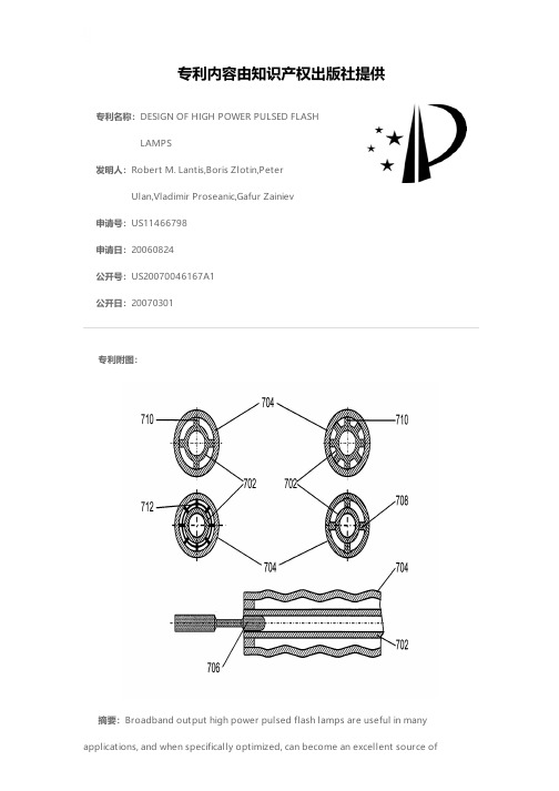
专利名称:DESIGN OF HIGH POWER PULSED FLASHLAMPS发明人:Robert M. Lantis,Boris Zlotin,PeterUlan,Vladimir Proseanic,Gafur Zainiev申请号:US11466798申请日:20060824公开号:US20070046167A1公开日:20070301专利内容由知识产权出版社提供专利附图:摘要:Broadband output high power pulsed flash lamps are useful in manyapplications, and when specifically optimized, can become an excellent source ofultraviolet (UV) light, which is particularly useful for photo-chemically-induced materials processing applications. Multiple factors involved with the production of high-energy light pulses can in certain cases adversely affect the ultraviolet lamp operation, thereby resulting in the development of micro cracks in lamp envelopes and subsequent limitation in lamp lifetime. Similar factors can be responsible for an increased absorption of UV radiation by lamp components and degradation of lamp efficiency. This invention describes new pulsed flash lamp designs that enable a new generation of high power and performance as required by, for example, many large-scale photo-processing applications. This invention uniquely and advantageously mitigates the development of micro-cracks and failure, and produces dramatically improved electrical efficiency, stability of lamp optical characteristics, and service lifetime.申请人:Robert M. Lantis,Boris Zlotin,Peter Ulan,Vladimir Proseanic,Gafur Zainiev地址:Ashburn VA US,West Bloomfield MI US,Wolverine Lake MI US,West Bloomfield MI US,West Bloomfield MI US国籍:US,US,US,US,US更多信息请下载全文后查看。
High power light-emitting diode

专利名称:High power light-emitting diode发明人:ファン バンホン申请号:JP2008000727申请日:20080213公开号:JP3141198U公开日:20080424专利内容由知识产权出版社提供专利附图:摘要:< Topic >It designates that as for this invention at cost, thermal resistance is low low in regard to the high power light-emitting diode, with simple production process,offers the satisfactory high power light-emitting diode of the heat dissipation effect as purpose.SolutionsThe high power light-emitting diode, has the transparency cover and the tip/chip and the base and the tab electrode and the heat dissipation fin. The said base is the compass bowl form which possesses the orbicular through hole in the center section, the said heat dissipation fin is laid out in the said orbicular through hole. Theinner wall of the aforementioned heat dissipation fin and the aforementioned through hole forms the illumination cup, the aforementioned tip/chip as it is laid out in the aforementioned illumination cup, is installed securely in the aforementioned heat dissipation fin, furthermore, one end of each aforementioned tab electrode has the sub -tab electrode of 2 at least. Heat dissipation is done by the heat dissipation fin and the tab electrode. Low the material of price is adopted and in order to decrease the thermal resistance of the heat dissipation system, low cost and heat dissipation are achieved.< Choice figure >Drawing 2申请人:フーシャンリデディエンズシーイエヨーシエンゴンス地址:中国 529728 グアンドンシェン フーシャンシ ゴンフーチェン国籍:CN代理人:高田 守,高橋 英樹更多信息请下载全文后查看。
一种恒流型DCDC大功率LED驱动电路的设计
本文由alwynchen0912贡献pdf文档可能在WAP端浏览体验不佳。
建议您优先选择TXT,或下载源文件到本机查看。
浙江大学电气工程学院硕士学位论文一种恒流型DC-DC大功率LED驱动电路的设计姓名:裴倩申请学位级别:硕士专业:电力电子与电力传动指导教师:陈辉明;王正仕20100127浙江大学硕士学位论文摘要摘要在能源和环境问题日趋严重的今天,以高效、节能、环保以及长寿命为主要特点的大功率照明白光LED获得了人们的重视。
随着其性能的提高以及生产成本的下降,大功率照明白光LED将逐步取代白炽灯和荧光灯,引起人类照明史上又一次革命。
与此同时,大功率从照明白光LED驱动电路的开发也由于大功率LED的应用的逐渐普及得到了长足的发展。
本论文的题目来源于电源公司的合作项目,论文的目的是设计一种市场需求量大的大功率白光LED恒流驱动变换器,要求其在输入电压和负载LED灯串电压(即个数)在一定范围内变化时,仍具有高恒流精度和控制结构简单、成本低、体积小、效率高等特点。
本论文的研究思路和工作内容如下:首先,论文对大功率照明LED的特性及发展和白光LED驱动电路的分类进行了介绍。
接着分析了DC-DC转换电路的原理和控制策略,包括DC-DC转换电路的三种拓扑结构的原理分析、两种反馈控制模式和三种控制方式。
然后,分析了本论文提出的大功率LED的Buck型、Boost型、Buck-Boost型变换器恒流输出的控制原理和恒流电路实现算法及结构。
最后,论文完成了各个单元电路的分析和设计,设计制作了一台用于驱动350mA、lW的白光LED--LuxeonTMStar的Buck型和Flyback型LED恒流DC-DC驱动变换器,并进行了调试实验和分析了各变量对恒流精度的影响,实验结果验证了本文理论研究和电路实现结构设计结果的正确性。
关键词:大功率LED;恒流驱动;开关电源;DC-DC转换电路浙江大学硕士学位论文摘要AbstractNowadaystheproblemsofenergysourcesandenvironmentbecomemoreandmoreserious,semiconductorlightinghaswonpeople’Sattentionforitsuniqueattributesoflowenergyconsumption,lowpollution,longlifeandhighefficiency.AsthequalityofpowerLEDimprovesandthecostofpowerLEDreduce,semiconductorlightingwillreplaceincandescentdevelopmentofHighPowerLED,theresearchofitsandfluorescentlightinggradually.Withtheconstantcurrentdrivingcircuithasalsobeengreatlyaccelerated.Thesourcesubjectofthedissertationoriginatesfromacooperativeprojectfundedbyapowercompany.ThedissertationaimstodesignaHighPowerLEDsconstantcurrentdrivingconverterwhichishighlydemandedbytheofmarket.TheainputvoltageandloadvoltageofLEDsastrings(i.e.numbersefficiencyisLEDs)changeswithincertainrange,Itisrequiredstillhavinghigh—precisionconstantcurrent.Andthecircuitstructureissimple,thecostislow,andthehigh.‘TheresearchCanbesummarizedasfollows:First,thefeaturesandthedevelopmentofhighpowerLEDlightingandtheclassificationofwhiteLEDdrivercircuitswereintroduced.ThenthethesisanalyzedtheprincipleandcontrolstrategyoftheDC-DCconvertercircuits,includingtheprinciplesanalysisofthethreecircuittopologies,twokindsoffeedbackcontrolmodescontrolprinciple,circuitconstant-currentoutputofconverterisandthreekindsofcontrolmode.Then,thealgorithmandcircuitstructure,beenpresentedinthispaper,oftheBuck-type,Boost-type,andBuck-Boosttypehigh?powerLEDanddesignofvariouscellcircuitisfinished.Aareanalyzed.Finally,theanalysisaBuck?-typeandFlyback?-typeLEDsconstantcurrentDC--DCdrivingconvertersetupforofdrivingseveral350mA,1variablesonWLuxeonTMStar.ExperimentsaccuracywerewerecarriedOutandtheimpactsaconstantcurrentanalyzed.Thedesign.experimentalresultshavegoodagreementwiththeoreticanalysisandcircuitstructure浙江大学硕上学位论文摘要Keyword:HighPowerLED;DC.DCconverterConstantcurrentdriver;Switchingmodepowersupply;浙江大学研究生学位论文独创性声明本人声明所呈交的学位论文是本人在导师指导下进行的研究工作及取得的研究成果。
多芯片阵列式高压发光二极管建模及其设计的开题报告
多芯片阵列式高压发光二极管建模及其设计的开题报告一、研究背景及意义高压发光二极管(High-voltage light-emitting diode,HV LED)由于其较高的工作电压和功率,逐渐成为照明应用和汽车照明应用等领域的新兴光源。
目前,市场上存在许多不同类型的HV LED,包括单个芯片、多芯片串联和并联阵列等不同结构。
其中,多芯片阵列式HV LED逐渐受到关注,因为它具有更高的亮度、更好的颜色均匀性和更高的可靠性。
因此,研究多芯片阵列式HV LED在理论和实践中的建模和设计对于提高其性能和降低成本至关重要。
二、研究内容和目标本文将研究多芯片阵列式HV LED的建模和设计。
具体研究内容包括以下几点:1. 首先,本文将对多芯片阵列式HV LED的物理特性进行研究和分析,包括多芯片串联和并联阵列HV LED的电气特性、光学特性和热特性等方面。
2. 然后,针对多芯片阵列式HV LED的特点,本文将建立一套完整的电路模型和光学模型。
通过模型分析,本文将研究多芯片阵列式HV LED的电气性能、光效和散热性能等方面。
同时,本文还将研究多芯片阵列式HV LED中各芯片之间的互相影响和优化方法。
3. 最后,本文将通过仿真和实验验证模型的正确性和可靠性。
并基于模型结果,设计出优化后的多芯片阵列式HV LED,以实现更高的亮度、更好的颜色均匀性和更高的可靠性。
三、研究方法本文将采用以下方法进行研究:1. 对多芯片阵列式HV LED的物理特性进行分析,包括电气特性、光学特性和热特性等方面,以建立完整的理论基础。
2. 基于理论分析结果,建立多芯片阵列式HV LED的电路模型和光学模型,通过模型分析多芯片阵列式HV LED的电气性能、光效和散热性能等方面,并找出各芯片之间的互相影响和优化方法。
3. 通过仿真和实验验证模型的正确性和可靠性,并基于模型结果,设计出优化后的多芯片阵列式HV LED。
四、计划进度和预期成果本文的计划进度如下:第一年:1. 对多芯片阵列式HV LED的物理特性进行研究和分析。
单片机英文参考文献(精选120个)

我国的单片机起步虽然较晚,但经过几十年的发展,也取得了巨大的成就。
不论是工业生产还是社会生活的各个方面都离不开单片机的使用。
下面是搜素整理的单片机英文参考文献的分享,以供参考。
单片机英文参考文献一: [1]Hui Wang. Optimal Design of Single Chip Microcomputer Multi-machine Serial Communication based on Signal VerificationTechnology[J]. International Journal of Intelligent Information and Management Science,2020,9(1)。
[2]Philip J. Basford,Steven J. Johnston,Colin S. Perkins,Tony Garnock-Jones,Fung Po Tso,Dimitrios Pezaros,Robert D. Mullins,Eiko Yoneki,Jeremy Singer,Simon J. Cox. Performance analysis of single board computer clusters[J]. Future Generation ComputerSystems,2020,102. [3]. Computers; Reports from University of Southampton Describe Recent Advances in Computers (Performance Analysis of Single Board Computer Clusters)[J]. Computers, Networks & Communications,2020. [4]Yunyu Cao,Jinjin Dang,Chenxu Cao. Design of Automobile Digital Tire Pressure Detector[J]. Journal of Scientific Research and Reports,2019. [5]Sudad J. Ashaj,Ergun Er?elebi. Reduce Cost Smart Power Management System by Utilize Single Board Computer Artificial Neural Networks for Smart Systems[J]. International Journal of Computational Intelligence Systems,2019. [6]Hanhong Tan*, Yanfei Teng. Design of PWM Lighting brightness Control based on LAN QIAO Cup single Chip Microcomputer[J]. International Journal of Computational and Engineering,2019,4(3)。
High power led module assembly and method for manu
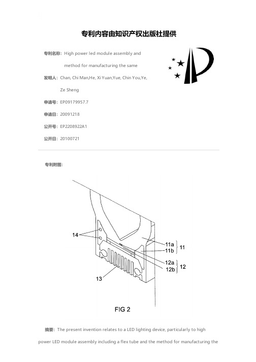
专利名称:High power led module assembly andmethod for manufacturing the same发明人:Chan, Chi Man,He, Xi Yuan,Yue, Chin You,Ye,Ze Sheng申请号:EP09179957.7申请日:20091218公开号:EP2208922A1公开日:20100721专利内容由知识产权出版社提供专利附图:摘要:The present invention relates to a LED lighting device, particularly to highpower LED module assembly including a flex tube and the method for manufacturing theassembly. The flex tube includes a base engaging with each of the high power LED modules and a cover partially enclosing the base, wherein the cover is made by extrusion process such that, except for the bottom of the heat sink exposed to ambient environment, the base, the high power LED module and other portions of the heat sink are enclosed by and hermetically engaged with the cover. With such configuration of the present invention, not only the heat dissipating property of the LED module assembly is enhanced but also the waterproof property thereof is further improved, thereby considerably extending the service life of the LED module assembly.申请人:Osram Gesellschaft mit beschränkter Haftung地址:Hellabrunner Strasse 1 81543 München DE国籍:DE更多信息请下载全文后查看。
DESIGN AND ANALYSIS OF HIGH-SPEED BRUSHLESS PERMANENT MAGNET MOTORS

Stator Diametrically
-1.5' 0
I
1
2
3
4
5
6
Anverlapping Concentrated Winding
Fig.3. Comparison of analytically and finite element predicted airgap field distributions.
of switching losses in the power electronic converter, which clearly favours a low pole number. As a result, 2-poles are often appropriate for high speed applications, a diametrically magnetised rotor often being preferred since it results in an essentially sinusoidal airgap flux density distribution. If the stator slot openings are neglected, the radial component of the open-circuit magnetostatic field in the airgap can be derived as:
where B, and p, are the remanence and relative recoil permeability of the magnet, and R,, R,, and R, are the radii of the stator bore, the rotor magnet and the rotor hub, respectively. Fig.1 shows a prototype 2-pole, 3-slot, 20,00Orpm, 200Vdc, 1.3kW, brushless dc motor, for which R, = 18.5mm, R, =9mm, R, = 17mm, B, = 1.2T, pr = 1.05, and the axial length 1, = 26”. Fig.2 shows instantaneous open-circuit flux distributions, whilst Fig.3 compares the analytically calculated airgap field with that predicted by finite element analysis when stator slotting is neglected. The stator winding inductances can have a significant effect on the dynamic performance of high-speed brushless drive systems [2-31. For example, they may cause the torque-speed curve to depart significantly from the ideal linear characteristic, which in turn may necessitate advancing the commutation in order to increase the high-speed torque capability. They also influence the maximum ripple current in PWM controlled systems, which in turn affects the motor losses and torque ripple. For brushless dc operation, the winding inductances can also cause the phase current to depart significantly from the ideal rectangular waveform, which can markedly reduce the torque capability at high speed and limit the maximum achievable speed [2]. However, the winding inductances of the prototype motor are relatively low, the values calculated using the analytical method described in [3] being 0.775mH and -0.32mH and the measured values being 0.872mH and -0.329mH, for the self- and mutual-inductances respectively. As a
提供高效电流的高亮度LED驱动设计
糍攀 E器 瓣黢热嚣 ,1帮嚣竣率,潦躲耱 链蹙瞧 囔懿 讴熊豫懿怒嚣斑黪嚣蹙 ≥ 罐 数热嚣姆槔壤窿 鳍手 蠢鳙A旗 张 惫嚣僚氆港 赣龟艇诒磐懿鼗耱藏 瓣
梅虢 的糍张 藏 畿懿簿簿铸鬻辩蕊黪
控制 电压与 三个并联检 流 电阻的 电
压共 同作 用到j 的反 馈( B 引脚 。 l的 C F) C
小 时 ,比传 统的 白炽灯 或卤素灯 的使 用
寿命高 出几 个数量 级。基 于这一 优势 ,
高亮度 L 在汽 车照 明、公共标 示与信 D E
号标志以及建筑照明中得到普遍应用。
图1 通过调节控 制电E ( _ 3 v ,M X 0 5L D电流驱动器能够 o  ̄ . ) A 5 3 E v 9 在L D A n E —K E _  ̄ D 端产 生近似3 0 _ mA的输出电流 L 5 mA ̄0
I … … 一 …… 一 … … … …… … …… … — — ~ { 一 } ~…一… } 一 …… …一 … ÷ ~ …
{
躺{ 娜
糍瀛鳇摊瓣 黪 激毂澎; 蝌臻 麟攘稚德 黼葬 觜 囊 糍 糍壤 畿姆爨潮 黢梅缝
雅蟾 £ 褥瞧姆鼗穗滋壤黪睽 凳 繁l 嬲 就 凡魄艨越麟,
6 西趸鄹 4 暖
1/0 8I, C 一 g m. m 20 、 门 z z c 1 v v州 o
黼
瑚臻 黪
瓤 溯 《 l 曦精 龇 趣 强 潞瑟
款基 于 电感的bu c 调节器能够准确控总 电压 为 E 或几 D E D
} l l l {
蝴
瓣褥 蠛 袋徽 一 巾嚣 髂 麟 怒》 燕然 蟪 黢懿粼 繇 酝耀 嚼 避瓣 端瓣 魄 撼 {
娩 堆 碗糍 艘黪 礁褥 l罐 张 器攫坐 暂 魅 蠖寝 绝 黾触 鱼瓣穗 糕 链囊 旗 檄缝 凇
STS静态转换开关说明书
www.borri.itSTS - STATIC TRANSFER SWITCHES BROCHUREBorri's R&D vast expertisein all facets of firmware, powerelectronics and mechanical designprovides innovative solutions fortomorrows problems in Industrial and Critical Power applications.The company prides itself onits first-class service and superiorengineering disciplines. To ensuresustained quality, Borri managesall its processes in house from feedstudies to design, production and after sales service technology. Based in Bibbiena, Italy with over 15,000 m² production area, Borri operates across all five continents with subsidiaries in USA, Canada, Germany, UAE, India and Malaysia. It has also established a strong distributor network, able to deliver on site support and technical guidance indicative of our own capabilities.The Borri Group has been developing and buildinguninterruptible power systems since 1932 and is a globalprovider of power electronics systems and solutions for harshindustrial and demanding critical power requirements.YOUR CRITICAL POWER SOLUTION PARTNER.BORRI | WHO WE ARE45STS | 16 A - 3000 Ato 3000 A STATIC TRANSFER SWITCHES 3-PHASE1-Phase and 3-Phase static transfer switches for seamless load transfer in dual path powersystems. The STS rugged design and high reliability provides supply redundancy and prevents fault propagation.Applications No break seamless transfers Automatically transferring loadsto alternative power sourceswhen the primary powersource fails or is not available.High availability Thanks to source separation, dual maintenance bypass and redundant crititical paths.Short circuit protectionEnsuring maximum sourceprotection in dual feedapplications.STS | 16 A - 3000 A 7Data centre Network& Server Industrial controls & processautomation1-phase static transfer switch series designed to offer solutions for the protection of single-phase loads.STS 16-32from 16 A to 32 A 16 A and 32 A version.6 x 40 A input terminal board.Zero switching time.supplies to controlboards, for increasedavailability. Redundant cooling and fan failure monitoring, for reliable operation.propagation. High overload capability, for robust electrical design. Comprehensive setof communicationoptions for total remotemonitoring of equipmentoperation. ITS maintenance switch.RS485 ModBusinterface.SNMP interface.Main optionsSTS block diagram ITS maintenance switchmain featuresSTS 16-32 front view STS 16 rear viewSTS 32 rear view 1-PHASE STATIC TRANSFER SWITCHES BYPASS 2BYPASS 1OUTPUT LOADSSTS 16-32 | 16 A - 32 A9protection.SCR fault detection andbackfeed protectionfor maximum upstreamsafety.Dual manual bypassfor complete sourceindependence duringmaintenance.True oversized neutral(2x In), redundantcooling with monitoredfans and redundant (3x3)internal power supply inComprehensive set of communication options for total remote monitoring of equipment operation. Fully compliance with all international product standards for maximum quality guarantee. Circuit breakers for reliable and safe tripping on all operating conditions.STS block diagramDry contact relay card(Included)To send UPS status to PLC’s,SCADA’s or AS400’s by voltagefree SPDT contacts RS485 ModBus-RTU port (Included)To send UPS status to BMS’s by RS485 connection and ModBus-RTU protocol. For remotemonitoring and remote serviceenvironment.Isolation transformer. Plug-in breakers. Output distribution panels. Panel builder version.Additional SPDT contactrelay board.4-pole configuration.Operation without neutral.Main optionsBYPASS 2BYPASS 1OUTPUT LOADSSTS 300 | 100 A - 3000 A 11Rating (A)*10025040063080010001250Dimensions WxDxH (mm)**820x835x14751220x860x19002000x1000x2100Weight (kg)**26529030561566010001450InputConnection type Hardwired 4wNominal voltage 208/380/400/415/440/480 Vac 3-phase with neutralVoltage tolerance ±10% (up to ±20% on request)Frequency and range 50/60 Hz, ±2 Hz (up to ±4 Hz on request)Source harmonic voltage contentUnlimited (if THD>20% transfer time ≤10ms)Transfer phase angle5° to 30°OutputConnection type Hardwired 4wNominal voltage 208/380/400/415/440/480 Vac 3-phase with neutralFrequency 50/60 Hz Transfer time ≤4 msTransfer mode Break before make, transfer inhibit on faultLoad power factor 1 to 0.3Maximum crest factor 3:1THD current feedback from loadUnlimitedOverload capacity***125% for 30 min, 150% for 10 min, 200% for 30 s, 2000% for 1 cycle, 4000% for ½ cycleEfficiency (AC/AC)>99%Connectivity and function extensionsFront panel Graphical LCD display, mimic LED panel and keyboard Remote communicationIncluded: dry contact relay card, RS232 and RS485 serial ports,ModBus-RTU protocol.Optional: additional dry contact relay cardOptional function extensions 4-pole configuration; plug-in circuit breakers;operation without neutral;panel builder execution;output distribution panels; isolation transformerSystemProtection degreeIP 20 (other options)Colour RAL 9005 (other options)Installation layout Wall, back to back and side by side installation allowedAccessibiltyFront access, bottom and top cable entry*rating up to 3000 A on request **3-pole version *** conditions applyEnvironmentalOperating temperature range 0°C to +40°C Storage temperature range-10°C to +70°CAltitude (AMSL)< 1000 m without power reduction, > 1000 m with reduction of 0.5% per 100 mAudible noise at 1 m (dBA)<62Standards and certifications Quality assurance, environment,health and safetyISO 9001:2015, ISO 14001:2015, BS OHSAS 18001:2007Safety IEC/EN 62310-1EMC IEC/EN 62310-2Breakers IEC/EN60947-3Transfer voltage limits IEEE Standard 446Protection degree IEC 60529Performance IEC/EN 62310-3MarkingCE STS 300 technical dataOther featuresSERVICE12Customer’s expectation defines Borri’s priority from the early analysis of the project requirements to a worldwide commissioning andservice. Many thousands of systems have been successfully installed and maintained globally, with continuous support from a highlytrained team of expert, certified technicians and engineers. From the professional set-up of Borri’s training centre or on site, the trainingand service team stand ready to provide support and contribute to tailored training at Borri or on site.You can be assured of Borrisupport to the highest standards no matter where in the world you are.Planning, installation, commissioningBorri assist you in every single step of your project. Our R&D team can analyse and develop solutions to a wide range of edge system requirements.Repair & spare partsAll spare parts supplied by Borri are original, tested and guaranteed to be fully compliant with Borri solutions.MaintenancePreventive maintenance guarantees uninterrupted operations and optimised system efficiency.TrainingBorri offers distributors and customers a service training structured in 3 levels. Courses can be held in Borri training centres or on-site.Analytical testsBorri undertakes a series of analytical tests in order to guarantee higher efficiency and continuity to your system operation. Remote monitoringGuardian Net remote monitoring system allows you to detect any deviation from optimum operation and trigger proper and immediate response, so that anomalies don’t evolve into issues.Battery testsBatteries have a limited time life and their proper maintenance is of high importance to guarantee efficiency to the UPS and avoid potential failures. Borri delivers high quality and performing batteries to assure smooth operations.SERVICE1314Extract fromOMG60326revC | 07-2022Due to our policy of continuous development, data in this document Since 1932,securing yourpower with passion and commitment.Asia Pacific Borri Asia PacificEngineering Sdn. Bhd.No.13, Jalan Serendah 26/41,Sekitar 26, Seksyen 26,40400 Shah Alam, Selangor MalaysiaTel. +60 3 5191 9098Fax +60 3 5103 8728********************IndiaBorri Power India Pvt. Ltd. Plot No. 69, Ground Floor Nagarjuna Hills, Panjagutta Hyderabad, 500 082IndiaTel. +91 40 2335 4095*************************BORRI SUBSIDIARIES AND SERVICE CENTRESBORRI HEADQUARTERS AND FACTORY Borri S.p.AVia 8 Marzo, 2 52011 Bibbiena (AR) ItalyTel. +39 0575 5351 Fax +39 0575 561811*************************www.borri.itMiddle East and Africa Borri PowerMiddle East FZCO1-151, Techno Hub PO Box: 342036Dubai Silicon Oasis, Dubai UAE Tel. +971 4 3200528Fax +971 4 3200529*************************AmericasBorri Power (US) Inc. 9000 Clay Road, Suit 104Houston, Texas, 77080USATel. +1 346 212 2686Fax +1 346 980 8875***************************。
Design and analysis of a high-speed comparator

P18
Shi Bo Institute for Infocomm Research Singapore
.sg
improve metastability behavior and reduce minimum differential input voltage. Implemented in a 0.35-pm SiGe BiCMOS process, the comparator consumes approximately 70mW with sampling speed of 16GHz and resolvable minimum input voltage of 8mV peak-to-peak
The comparator input-referred noise consists primarily of the thermal and shot noise of the transistors Q3 and Q4 and the thermal noise of the resistors RL. From [2], the spectral density of the noise is
Index Terms-High-speed comparator design, analog-to-digital converters, flash ADC design, bipolar IC design.
1. INTRODUCTION With more interests in Ultra Wideband (UWB) Communications, the analog-to-digital converters (ADC) used in this area also require very high sampling speed. Flash ADCs are known to be one of the fastest possible converters. But the performance of a flash ADC strongly depends on that of their constituent comparators. For an n-bit flash ADC, 2- I comparators are needed. Therefore, how to increase the comparator speed while not increasing power dissipation too much is a challenge to the designer. Another challenge is that the resolvable minimum differential input should not be too large such that a flash ADC with moderate resolution can be built. To reduce minimum input, input referred offset must also be reduced. This paper presents a master-slave comparator which tries to increase the sampling speed and reduce minimum differential input voltage while maintaining power dissipation at a relatively low level. The final comparator design has a very high speed of 16 GHz clock rate with post-layout simulation. Compared with previous work [1], the comparator presented here has a comparable operating speed with less power consumption and lower minimum input difference.
大功率LED的热阻测量与结构分析

1.1电学参数法
目前国内外测量LED热学特性的方法主要有
冷却曲线相互对称,两者均能反映LED的热性能, 因此在实验中宜采用测量冷却曲线的方法阴,具体步 骤如下(参见图1):
温度可控
红外热成像法、光谱法、光功率法、管脚温度法和电
学参数法。采用电学参数法测量时,LED的PN结既
是被测对象,又是温度传感器,消除了因附加温度传
由于仪器功能的原因,在测量LED热阻时,要
么直接忽略了LED的光功率‰嘲,要么仅对LED
(8)
z
的光功率进行粗略的估计”a,这对于输入电能约有
10%~30%转化为光能的大功率LED来说将导致 较大的测量偏差。还有另外一种方法是分别用两套
式中c£2
J。c(f)A(f)df;R
2
J。南
X
1
面旨df;c为体积热容;A为热导率;A为热传导
Of measuring thermaI resistance fOr high—power LED was prOpOsed.The inner—construction details Of high—power LED,such
as
d”nension,materiaI,manUfacture defects and assembly
式中L为待测LED未施加加热功率前的初始
26现代显示Adv粕ced
Display
Au昏,20鹏,总第9l期
万方数据
庄鹏:大功率LED的热阻测量与结构分析
LED的热阻为
‰=等等
1.2结构函数的推导过程
联组成的简单热学系统,产生的温度响应为:
㈣
技 术 交 流
图3 R7 e1
Foster热学模型
无线电力传输的电车辆应用-英文
Wireless Power Transfer for Electric Vehicle ApplicationsSiqi Li,Member,IEEE,and Chunting Chris Mi,Fellow,IEEEAbstract—Wireless power transfer(WPT)using magnetic resonance is the technology which could set human free from the annoying wires.In fact,the WPT adopts the same basic theory which has already been developed for at least30 years with the term inductive power transfer.WPT tech-nology is developing rapidly in recent years.At kilowatts power level,the transfer distance increases from several mil-limeters to several hundred millimeters with a grid to load efficiency above90%.The advances make the WPT very attractive to the electric vehicle(EV)charging applications in both stationary and dynamic charging scenarios.This paper reviewed the technologies in the WPT area applicable to EV wireless charging.By introducing WPT in EVs,the obstacles of charging time,range,and cost can be easily mitigated.Battery technology is no longer relevant in the mass market penetration of EVs.It is hoped that researchers could be encouraged by the state-of-the-art achievements,and push forward the further development of WPT as well as the expansion of EV.Index Terms—Dynamic charging,electric vehicle(EV), inductive power transfer(IPT),safety guidelines,stationary charging,wireless power transfer(WPT).I.I NTRODUCTIONF OR energy,environment,and many other reasons,theelectrification for transportation has been carrying out for many years.In railway systems,the electric locomotives have already been well developed for many years.A train runs on a fixed track.It is easy to get electric power from a conductor rail using pantograph sliders.However,for electric vehicles(EVs), the highflexibility makes it not easy to get power in a similar way.Instead,a high power and large capacity battery pack is usually equipped as an energy storage unit to make an EV to operate for a satisfactory distance.Until now,the EVs are not so attractive to consumers even with many government incentive ernment subsidy and tax incentives are one key to increase the market share of EV today.The problem for an electric vehicle is nothing else but the electricity storage technology,which requires a battery which is the bottleneck today due to its unsatisfactory energy density,limited life time and high cost. Manuscript received February2,2014;revised April6,2014;accepted April18,2014.Date of publication April23,2014;date of current ver-sion January29,2015.Recommended for publication by Associate Editor ler.S.Li is with the Department of Electrical Engineering,Kunming Uni-versity of Science and Technology,Kunming650500,China(e-mail: lisiqi@).C. C.Mi is with the Department of Electrical and Computer Engineering,University of Michigan,Dearborn,MI48128USA(e-mail: chrismi@).Color versions of one or more of thefigures in this paper are available online at .Digital Object Identifier10.1109/JESTPE.2014.2319453In an EV,the battery is not so easy to design because of the following requirements:high energy density,high power density,affordable cost,long cycle life time,good safety, and reliability,should be met simultaneously.Lithium-ion batteries are recognized as the most competitive solution to be used in electric vehicles[1].However,the energy density of the commercialized lithium-ion battery in EVs is only 90–100Wh/kg for afinished pack[2].1This number is so poor compared with gasoline,which has an energy density about 12000Wh/kg.To challenge the300-mile range of an internal combustion engine power vehicle,a pure EV needs a large amount of batteries which are too heavy and too expensive. The lithium-ion battery cost is about500$/kWh at the present time.Considering the vehicle initial investment,maintenance, and energy cost,the owning of a battery electric vehicle will make the consumer spend an extra1000$/year on average compared with a gasoline-powered vehicle[1].Besides the cost issue,the long charging time of EV batteries also makes the EV not acceptable to many drivers.For a single charge, it takes about one half-hour to several hours depending on the power level of the attached charger,which is many times longer than the gasoline refueling process.The EVs cannot get ready immediately if they have run out of battery energy. To overcome this,what the owners would most likely do is tofind any possible opportunity to plug-in and charge the battery.It really brings some trouble as people may forget to plug-in andfind themselves out of battery energy later on. The charging cables on thefloor may bring tripping hazards. Leakage from cracked old cable,in particular in cold zones, can bring additional hazardous conditions to the owner.Also, people may have to brave the wind,rain,ice,or snow to plug-in with the risk of an electric shock.The wireless power transfer(WPT)technology,which can eliminate all the charging troublesome,is desirable by the EV owners.By wirelessly transferring energy to the EV,the charging becomes the easiest task.For a stationary WPT system,the drivers just need to park their car and leave.For a dynamic WPT system,which means the EV could be powered while driving;the EV is possible to run forever without a stop. Also,the battery capacity of EVs with wireless charging could be reduced to20%or less compared to EVs with conductive charging.Although the market demand is huge,people were just wondering whether the WPT could be realized efficiently at1Although lithium ion battery can achieve up to200Wh/kg for individual cells,the battery pack requires structure design,cooling,and battery manage-ment systems.The over energy density of a battery pack is much lower than the cell density.2168-6777©2014IEEE.Personal use is permitted,but republication/redistribution requires IEEE permission.See /publications_standards/publications/rights/index.html for more information.a reasonable cost.The research team from MIT published a paper in Science[3],in which60W power is transferred at a2-m distance with the so called strongly coupled magnetic resonance theory.The result surprised the academia and the WPT quickly became a hot research area.A lot of interesting works were accomplished with different kinds of innovative circuit,as well as the system analysis and control[4]–[9].The power transfer path can even be guided using the domino-form repeaters[10],[11].In order to transfer power more efficiently and further,the resonant frequency is usually selected at MHz level,and air-core coils are adopted.When the WPT is used in the EV charging,the MHz frequency operation is hard to meet the power and efficiency criteria.It is inefficient to convert a few to a few hundred kilowatts power at MHz frequency level using state-of-the-art power electronics devices.Moreover,air-core coils are too sensitive to the surrounding ferromagnetic objects.When an air-core coil is attached to a car,the magneticflux will go inside the chassis causing high eddy current loss as well as a significant change in the coil parameters.To make it more practical in the EV charging,ferrite as a magneticflux guide and aluminum plate as a shield are usually adopted in the coil design[12].With the lowered frequency to less than100kHz, and the use of ferrite,the WPT system is no different from the inductive power transfer(IPT)technology which has been developed for many years[13]–[39].In fact,since the WPT is based on the nonradiative and near-field electromagnetic,there is no difference with the traditional IPT which is based on magneticfield coupling between the transmitting and receiving coils.The IPT system has already been proposed and applied to various applications,such as underwater vehicles[32]–[34], mining systems[16],cordless robots in automation production lines[36]–[39],as well as the charging of electric vehicles [13],[14],[25]–[27].Recently,as the need of EV charging and also the progress in technology,the power transfer distance increases from several millimeters to a few hundred millimeters at kilowatts power level[12],[14],[40]–[60].As a proof-of-concept of a roadway inductively powered EV,the Partners for Advance Transit and Highways(PATH)program was conducted at the UC Berkeley in the late1970s[14],[54].A60kW, 35-passanger bus was tested along a213m long track with two powered sections.The bipolar primary track was supplied with1200A,400Hz ac current.The distance of the pickup from the primary track was7.6cm.The attained efficiency was around60%due to limited semiconductor technology.During the last15years,researchers at Auckland University have focused on the inductive power supply of movable objects. Their recent achievement in designing pads for the stationary charging of EV is worth noting.A766mm×578mm pad that delivers5kW of power with over90%efficiency for distances about200mm was reported[48],[55].The achieved lateral and longitudinal misalignment tolerance is 250and150mm,respectively.The knowledge gained from the on-line electric vehicle(OLEV)project conducted at the Korea Advanced Institute of Science and Technology(KAIST) also contributes to the WPT design.Three generations of OLEV systems have been built:a light golf cart as thefirst Fig.1.Typical wireless EV charging system.generation,a bus for the second,and an SUV for the third. The accomplishment of the second and the third is noteworthy: 60kW power transfer for the buses and20kW for the SUVs with efficiency of70%and83%,respectively;allowable vertical distance and lateral misalignment up to160mm and up to200mm,respectively[56],[57].In the United States, more and more public attention was drawn to the WPT since the publication of the2007Science paper[3].The WiTricity Corporation with technology from MIT released their WiT-3300development kit,which achieves90%efficiency over a 180mm gap at3.3kW output.Recently,a wireless charging system prototype for EV was developed at Oak Ridge National Laboratory(ORNL)in the United States.The tested efficiency is nearly90%for3kW power delivery[53].The research at the University of Michigan–Dearborn achieved a200mm distance,8kW WPT system with dc to dc efficiency as high as95.7%[61].From the functional aspects,it could be seen that the WPT for EV is ready in both stationary and dynamic applications.However,to make it available for large-scale commercialization,there is still abundant work to be done on the performance optimization,setup of the industrial standards, making it more cost effective,and so on.This paper starts with the basic WPT theory,and then gives a brief overview of the main parts in a WPT system, including the magnetic coupler,compensation network,power electronics converter,study methodology,and its control,and some other issues like the safety considerations.By introduc-ing the latest achievements in the WPT area,we hope the WPT in EV applications could gain a widespread acceptance in both theoretical and practical terms.Also,we hope more researchers could have an interest and make more brilliant contributions in the developing of WPT technology.II.F UNDAMENTAL T HEORYA typical wireless EV charging system is shown in Fig.1. It includes several stages to charge an EV wirelessly.First, the utility ac power is converted to a dc power source by an ac to dc converter with power factor correction.Fig.2.General two-coil WPT system.Then,the dc power is converted to a high-frequency ac todrive the transmitting coil through a compensation network.Considering the insulation failure of the primary side coil,a high-frequency isolated transformer may be inserted betweenthe dc-ac inverter and primary side coil for extra safety andprotection.The high-frequency current in the transmitting coilgenerates an alternating magneticfield,which induces an acvoltage on the receiving coil.By resonating with the secondarycompensation network,the transferred power and efficiencyare significantly improved.At last,the ac power is rectifiedto charge the battery.Fig.1shows that a wireless EV chargerconsists of the following main parts:1)the detached(or separated,loosely coupled)transmittingand receiving ually,the coils are built withferrite and shielding structure,in the later sections,theterm magnetic coupler is used to represent the entirety,including coil,ferrite,and shielding;2)the compensation network;3)the power electronics converters.The main difference between a wireless charger and aconventional conductive or wired charger is that a transformeris replaced by a set of loosely couple coils.To give a quickidea of the WPT principle,the coil and the compensationnetwork are pulled out separately,as shown in Fig.2,whereL1represents the self-inductance of the primary side transmit-ting coil and L2represents the self-inductance of the receivingcoil;˙I1and˙I2are the current in the two coils;˙U12is thevoltage in the secondary coil that is induced by the currentin the primary side coil.˙U21is the voltage in the primarycoil that is induced by the current in secondary side coil dueto coupling,or mutual inductance between the primary andsecondary coils.S1and S2are the apparent power goes intoL1and L2,respectively.S3and S4are the apparent powerprovided by the power converter.S12and S21represent theapparent power exchange between the two coils.The form ofthe compensation network is not specified.The characteristicsof the compensation network will be discussed later.As shown in Fig.2,neglecting the coil resistance andmagnetic losses,we can calculate the simplified form ofexchanged complex power from L1to L2˙S12=−˙U12˙I∗2=−jωM˙I1˙I∗2=ωM I1I2sinϕ12−jωM I1I2cosϕ12(1)˙S21=−˙U21˙I∗1=−jωM˙I2˙I∗1=−ωM I1I2sinϕ12−jωM I1I2cosϕ12(2)where I1and I2are the root mean square value andϕ12isthe phase difference between˙I1and˙I2.The active powertransfer from the primary side to the secondary side can beexpressed asP12=ωM I1I2sinϕ12.(3)The system shown in Fig.2can transfer active power inboth directions.In the analysis below,we assume the poweris transferred from L1to L2.Whenϕ12=π/2,which means˙I1leads˙I2by a quarter cycle,the maximum power can betransferred from L1to L2.The total complex power goes into the two-coil system is˙S=˙S1+˙S2=jωL1˙I1+ωM˙I2˙I∗1+jωL2˙I2+ωM˙I1˙I∗2=jωL1I21+L2I22+2M I1I2cosϕ12.(4)Therefore,the total reactive power goes into the two-coilsystem isQ=ωL1I21+L2I22+2M I1I2cosϕ12.(5)For a traditional transformer,the reactive power representsthe magnetizing power.Higher magnetizing power bringshigher copper and core loss.To increase the transformerefficiency,the ratio between the active power and reactivepower should be maximized.The ratio is defined byf(ϕ12)=|P12||Q|=ωM I1I2sinϕ12ωL1I21+ωL2I22+2ωM I1I2cosϕ12=k1−cos2ϕ12L1L2I1I2+L2L1I2I1+2k cosϕ21=k1−cos2ϕ12x+1x+2k cosϕ12(6)whereπ/2<ϕ12<πx=L1L2I1I2>0k is the coupling coefficient between L1and L2.To achieve the maximum value of f(ϕ12),we solve thefollowing equations:∂∂ϕ12f(ϕ12)=0,∂2∂2ϕ12f(ϕ12)<0(7)and the solutions arecosϕ12=−2kx+1x,sinϕ12=1−4k2x+1x2.(8)When k is close to1,it is a traditional transformer.In this case,if˙I2is an induced current by˙I1,x will be close to1. Thus,cosϕ12≈−1.The phase difference between˙I1and˙I2 is nearly180°.While for WPT,k is close to0.f(ϕ12)is maximized at sinϕ12=1,at which point the transferred power is also maximized.The phase between˙I1and˙I2is around90°instead of180°.Hence we can see the difference between the tightly and the loosely coupled coils.The degree of coupling affects the design of the compensa-tion network.Taking the series–series topology as an example, there are two ways to design the resonant capacitor.One way is design the capacitor to resonate with the leakage inductance [46],[62]which could achieve a higher f(ϕ12).Another way is to resonate with the coil self-inductance[27],[41],[63] which could maximum the transferred power at a certain coil current.When the coupling is tight with a ferrite,like k>0.5, it is important to increase f(ϕ12)to achieve better efficiency. In this case,resonate with the coil self inductance,which makesϕ12=π/2and lowers f(ϕ12),is not recommended. Otherwise the magnetizing loss may significantly increase. When the capacitor resonates with the leakage inductance,it is like the leakage inductance is compensated.This makes the transformer perform as a traditional one and increases f(ϕ12). However,the overall system does not work at a resonant mode.When the coupling is loose,like k<0.5,which is the case for the EV wireless charging,usually the capacitor is tuned with the self inductance to make the system working at a resonate mode to achieve maximum transferred power at a certain coil current.In this case,most of the magnetic field energy is stored in the large air gap between the two coils.The hysteresis loss in the ferrite is not so relative to the magnetizing power.However,the loss in the copper wire is proportional to the square of the conducting current. To efficiently transfer more power at a certain coil current,the induced current˙I2should lag˙I1by90°.Since the induced voltage˙U12on the receiving coil lags˙I1by90°,˙U12and˙I2 should be in phase.The secondary side should have a pure resistive characteristic seen from˙U12at the frequency of˙I1. At the meanwhile,the primary side input apparent power S3 should be minimized.At cosϕ12=0,the complex power˙S1is˙S1=jωL1I21+ωM I1I2.(9) Ideally,the primary side compensation network should cancel the reactive power and make S3=ω0M I1I2,where ω0is the resonant frequency.From the above analysis,we see for a certain transferred power,it is necessary to make the secondary side resonant to reduce the coil volt-ampere(V A) rating,which reduces the loss in the coils;and to make the primary side resonant to reduce the power electronics converter V A rating,which reduces the loss in the power converter. Therefore,we transfer power at the magnetic resonance. With the above analysis,we can calculate the power transfer efficiency between the two coils at the resonant frequency.We haveU12=I2(R2+R Le)=ωM I1=ωkL1L2I1(10) where R2is the secondary winding resistance and R Le is the equivalent load resistance.By defining the quality factor of the two coils, Q1=ωL1/R1,Q2=ωL2/R2,the transferred efficiency can be expressed asη=I22R LeI21R1+I22R2+I22R Le=R Le(R2+R Le)2k2Q1Q2R2+R2+R Le.(11)By defining a=R Le/R2,we obtain the expression of efficiency as a function of aη(a)=1a+1a+2k2Q1Q2+1a+1.(12)The maximum efficiency is obtained by solving the follow-ing equations:∂∂aη(a)=0,∂2∂2aη(a)<0.(13) The maximum efficiencyηmax=k2Q1Q21+1+k2Q1Q22is achieved at aηmax=1+k2Q1Q21/2.In[64],the maximum efficiency is also derived based on several different kinds of compensation network.The results are identical and accord with the above results.The analysis here does not specify a particular compensation form.It can be regarded as a general formula to evaluate the coil performance and estimate the highest possible power transfer efficiency. In EV wireless charging applications,the battery is usu-ally connected to the coil through a diode-bridge rectifier. Most of the time,there is some reactive power required. The reactive power can be provide by either the coil or the compensation network like a unit-power-factor pickup.The battery could be equivalent to a resistance R b=U b/I b,where U b and I b is the battery voltage and current,respectively. If the battery is connected to the rectifier directly in a series-series compensation form,the equivalent ac side resistance could be calculated by R ac=8/π2·R b.Thus,a battery load could be converted to a resistive load.The R ac equation is different for different battery connection style,like with or without dc/dc converter,parallel or series compensation. Most of the time,the equivalent R ac could be derived.Some typical equivalent impendence at the primary side is given in paper[42].By calculating the equivalent ac resistances,the above equations could also be applied to a battery load with rectifier.For stationary EV wireless charging,the coupling between the two coils is usually around0.2.If both the sending and receiving coils have a quality factor of300,the theoretical maximum power transfer efficiency is about96.7%.More efficiency calculations under different coupling and quality factors are shown in Fig.3.Fig.3.Theoretical maximum transfer efficiency between two coils.III.M AGNETIC C OUPLER D ESIGNTo transfer power wirelessly,there are at least two magnetic couplers in a WPT system.One is at the sending side,named primary coupler.The other is at the receiving side,named pickup coupler.Depending on the application scenarios,the magnetic coupler in a WPT for an EV could be either a pad or a track form.For higher efficiency,it is important to have high coupling coefficient k and quality factor Q. Generally,for a given structure,the larger the size to gap ratio of the coupler is,the higher the k is;the thicker the wire and the larger the ferrite section area is,the higher the Q is. By increasing the dimensions and materials,higher efficiency can be achieved.But this is not a good engineering approach. It is preferred to have higher k and Q with the minimum dimensions and cost.Since Q equalsωL/R,high frequency is usually adopted to increase the value of Q.The researchers at Massachusetts Institute of Technology(MIT)used a frequency at around10MHz and the coil Q value reached nearly 1000[3].In high power EV WPT applications,the frequency is also increased to have these benefits.In Bolger’s early design,the frequency is only180Hz[13].A few years later, a400Hz frequency EV WPT system was designed by System Control Technology[14].Neither180Hz nor400Hz is high enough for a loosely coupled system.Huge couplers were employed in the two designs.Modern WPT system uses at least10kHz frequency[15].As the technical progress of power electronics,100kHz could be achieved[65]at high power level.The WiTricity Company with the technology from MIT adopts145kHz in their design.In the recent researches and applications,the frequency adopted in an EV WPT system is between20and150kHz to balance the efficiency and cost.At this frequency,to reduce the ac loss of copper coils, Litz wire is usually adopted.Besides the frequency,the coupling coefficient k is sig-nificantly affected by the design of the magnetic couplers, which is considered one of the most important factors in a WPT system.With similar dimensions and materials,different coupler geometry and configuration will have a significant difference of coupling coefficient.A better coupler design may lead to a50%–100%improvement compared with some nonoptimal designs[48].Fig.4.Mainflux path of double-sided and single-sided coupler.(a)Double-sided type.(b)Single-sided type.A.Coupler in the Stationary ChargingIn a stationary charging,the coupler is usually designed in a pad form.The very early couplers are just like a simple split core transformer[19],[38],[56].Usually this kind of design could only transfer power through a very small gap. To meet the requirements for EV charging,the deformations from spilt core transformers and new magnetic coupler forms are presented for large gap power transfer[12],[31],[37],[42], [47]–[50],[66]–[71].According to the magneticflux dis-tribution area,the coupler could be classified as the double-sided and single-sided types.For the double-sided type,theflux goes to both sides of the coupler[12], [31],[67].Aflattened solenoid inductor form is pro-posed in[12]and[67].Because theflux goes through the ferrite like through a pipe,it is also called aflux-pipe coupler.To prevent the eddy current loss in the EV chassis,an aluminum shielding is usually added which bring a loss of1%–2%[12].When the shielding is added, the quality factor of aflux-pipe coupler reduces from 260to86[48].The high shielding loss makes the double-sided coupler not the optimal choice.For the single-sided coupler, most of theflux exists at only one side of the coupler.As shown in Fig.4,the mainflux pathflows through the ferrite in a single-sided coupler.Unlike the double-sided coupler having half of the mainflux at the back,the single-sided coupler only has a leakageflux in the back.This makes the shielding effort of a single-sided type much less.Two typical single-sidedflux type pads are shown in Fig.5. One is a circular unipolar pad[47].Another one is a rectan-gular bipolar pad proposed by University of Auckland,which is also named DD pad[48].Besides the mechanical support material,a single-sided pad is composed of three layers.The top layer is the coil.Below the coil,a ferrite layer is inserted for the purpose of enhancing and guiding theflux.At the bottom is a shielding layer.To transfer power,the two pads are put closed with coil to coil.With the shielding layer, most of the high-frequency alternating magneticflux can be confined in the space between the two pads.A fundamental flux path concept was proposed in theflux pipe paper[67].Fig. 5.Two typical single-sidedflux type pads.(a)Circular pad.(b)DD pad.Theflux path height of a circular pad is about one-fourth ofthe pad’s diameter.While for a DD pad,the height is abouthalf of the pad’s length.For a similar size,a DD pad has asignificant improvement in the coupling.The charge zone fora DD pad could be about two times larger than a circular padwith similar material cost.The DD pad has a good tolerant inthe y-direction.This makes the DD pad a potential solutionfor the dynamic charging when the driving direction is alongwith the y-axis.However,there is a null point for DD pad inthe x-direction at about34%misalignment[48].To increasethe tolerant in x-direction,an additional quadrature coil namedQ coil is proposed to work together with the DD pad,whichis called DDQ pad[48],[49],[68].With a DDQ receivingpad on a DD sending pad,the charge zone is increased tofivetimes larger than the circular configuration.As the additionalQ coil in the receiver side,the DDQ over DD configurationuses almost two times copper compared with the circularone[48].A variant of a DDQ pad,which is called a newbipolar pad,was also proposed by University of Auckland[49],[50].By increasing the size of each D pad and havingsome overlap between the two D coils,the new bipolar padcould have a similar performance of a DDQ pad with25%less copper.With all the efforts,at200mm gap,the cou-pling between the primary and secondary pads could achieve0.15–0.3with an acceptable size for an EV.Referred to Fig.3,at this coupling level,efficiency above90%could possibly beachieved.B.Coupler in the Dynamic ChargingThe dynamic charging,also called the OLEVs[56]orroadway powered electric vehicles[14],is a way to chargethe EV while driving.It is believed that the dynamic chargingcan solve the EVs’range anxiety,which is the main reasonlimits the market penetration of EVs.In a dynamic chargingsystem,the magnetic components are composed of a primaryside magnetic coupler,which is usually buried under the road,and a secondary side pickup coil,which is mounted under anEV chassis.There are mainly two kinds of primary magneticcoupler in the dynamic charging.Thefirst kind is a long trackcoupler[26],[31],[57],[70],[72]–[76].When an EV withaFig.6.Top view of W-shape and I-shape track configuration.pickup coil is running along with the track,continues powercan be transferred.The track can be as simple as just twowires[37],[77],or an adoption of ferrites with U-type orW-type[26],[56]to increase the coupling and power trans-fer distance.Further,a narrow-width track design with anI-type ferrite was proposed by KAIST[72],[73].The dif-ferences between the W-type and I-type are shown in Fig.6.For W-type configuration,the distribution area of the ferrite Wdetermines the power transfer distance,as well as the lateraldisplacement.The total width of W-type should be about fourtimes the gap between the track and the pickup coil.For I-typeconfiguration,the magnetic pole alternates along with the road.The pole distance W1is optimized to achieve better coupling atthe required distance.The width of pickup coil W2is designedto meet the lateral misalignment requirement.The relationbetween track width and transfer distance is decoupled andthe track can be built at a very narrow form.The width forU-type and W-type is140and80cm,respectively[73].ForI-type,it could be reduced to only10cm with a similar powertransfer distance and misalignment capacity.35kW power wastransferred at a200mm gap and240mm displacement usingthe I-type configuration[73].With the narrowed design,theconstruction cost could be reduced.Also,the track is far awayfrom the road side,the electromagneticfield strength exposedto pedestrians can also be reduced.The problem of the track design is that the pickup coil onlycovers a small portion of the track,which makes the couplingcoefficient very small.The poor coupling brings efficiencyand electromagnetic interference(EMI)issues.To reduce theEMI issue,the track is built by segments[52],[70],[75]with a single power converter and a set of switches to powerthe track.The excitation of each segment can be controlledby the switches’ON-OFF state.The electromagneticfieldabove the inactive segments is reduced significantly.However,there is always a high-frequency currentflowing through thecommon supply cables,which lowers the system efficiency.The published systems efficiency is about70%–80%,whichis much lower than the efficiency achieved in the stationarycharging.When each segment is short enough,the track becomes likea pad in the stationary charging,which is the other kind ofthe primary magnetic coupler.Each pad can be driven by anindependent power converter.Thus,the primary pads can beselectively excited without a high-frequency common current.Also,the energized primary pad is covered by the vehicle.Theelectromagneticfield is shielded to have a minimum impact。
- 1、下载文档前请自行甄别文档内容的完整性,平台不提供额外的编辑、内容补充、找答案等附加服务。
- 2、"仅部分预览"的文档,不可在线预览部分如存在完整性等问题,可反馈申请退款(可完整预览的文档不适用该条件!)。
- 3、如文档侵犯您的权益,请联系客服反馈,我们会尽快为您处理(人工客服工作时间:9:00-18:30)。
长 × 宽 × 厚 ( mm) 导热铝板 散热片 散热片基板 50 × 93 × 8 30 × 93 × 1 145 × 93 × 5
2 ) 第二种 LED 车前照灯模型结构建立 如图 2 所示,所设计的第二种 LED 车前照灯结 构为圆形散热装置,其散热片采用圆形散热翅片,其 依次组成部分为 9 个 10W 的 LED、铝基板、导热胶、 圆形散热翅片等组成,为了考虑车灯内部体积的容易 安装,且易于在圆形翅片底部加装风扇,故设计成圆 形结构模式。散热器的外形尺寸如表 2 所示。
3 ) 第三种 LED 车前照灯模型结构建立 如图 3 所示,其所设计的第三种 LED 车前照灯
第 24 卷第 6 期
陈文林等: 大功率 LED 汽车前照灯散热装置的设计与分析
103
定义单元类型; ② 定义材料属性; ③ 划分网格; ④ 施加热载荷与定义边界条件; ⑤ 求解并查看结果。 根据以上步骤分别对前面设计的三种散热结构在自 然对流和强迫对流 ( 加装散热风扇 ) 情况下进行热 分析研究。 3. 1 导热板方案的热分析研究 在进行热仿真分析时,材料热导率为: 铝 237W (m · K) ,导热硅胶 2W( m · K) ,PCB 板 200W( m · K) ,
[6 ] [2 ]
1 ) 第一种 LED 车灯结构模型的建立 如图 1 所示,LED 车前照灯由 90 个 1W 的大功 率 LED、铝基板 PCB、导热板、导热硅胶和散热片组 成。在相互连接的两层面之间添加导热硅胶使其粘 连,增加两个部分之间的传热,降低其热阻。其中, 在每两个部件之间添加导热硅胶厚度为 0. 5mm,导热 · K) ,采用铝板作为导热板。室 硅胶导热率为 2W( m · K ) 。其中导热铝板 温下,铝的热导率为 237 W( m 和散热片的尺寸如表 1 所示,这一结构尺寸主要是考 虑到与车前灯的整体形状和尺寸配合。
Abstract : With the inceasing improvement of LED manufacturing technology,the high power white LED is gradually applied in the field of all kinds of lighting . But with increasing working time of LED chips,their junctions' temperature keep increasing,led to lightemitting efficiency and chip reliability decreaseand even failure. In this paper three cooling devices were designed by PROE aiming to the serious fever of LED chips. We analysed three kinds of radiators under the condition of natural convection and forced convection heat using ANSYS software respectively,and determined eventually to adopt the scheme of warm plate heat dissipation of the forced convection through comparing. Experiments of lighting the LED car headlamps for five hours show that the LED chip junctions' temperature measured are less than 80℃ and we can solve the problem of high power LED car headlamps heat dissipation s effectively. Key words: Radiator; ANSYS; LED; headlamps LED 一般功率较小,不存在散热问题。而后,随着国
图4 Fig. 4
自然对流芯片温度分布图 distribution of chip
The natural convection temperature
图3 Fig. 3
第三种 LED 车前照灯模型结构
The third structure model of LED headlamp
表 3 散热器的结构尺寸 Table 3 the radiator structure size
时间的推移,其结温不断升高,导致 LED 芯片发光效率和可靠性不断降低,甚至失效。本文针对 LED 芯片发热严重 的问题,运用 PROE 设计了三款 90W 汽车前照灯及散热装置; 运用 ANSYS 分析软件分别对三种散热装置在自然对流 和强制对流条件下进行热分析,通过对比最终确定采用强制对流均温板式散热方案。对设计的前照灯进行实验测试, 车前灯连续工作 5 个小时,测得 LED 芯片结温始终小于 80℃ ,有效地解决了大功率 LED 汽车前照灯的散热问题。 关键词: 散热装置; ANSYS; LED; 前照灯 中图分类号: U463. 65 + 1 文献标识码: A DOI: 10. 3969j. issn. 1004440X. 2013. 06. 019
在汽车领域。21 世纪初,人类就将 LED 应用于车内 仪表盘信号灯指示等小功率照明上,该领域所用的
基金项目: 沈阳市人才资源开发专项资金资助项目 ( 2012010403 )
102
照明工程学报
2013 年 12 月
灯,再者是刹车灯等。目前一些高档轿车公司,比如 [ 1 ] 宝马、奔驰、奥迪、丰田 等已经将大功率高亮度 LED 前照灯商品化,而不是仅仅局限于一些概念车领 域了。截止目前,中国市场内仍然有很少前照灯专门 研发企业,其中最大的难题就是 LED 的散热问题。 针对汽车前照灯散热器的研究, 现在国内外已 经取得了一些成绩。2002 年, 通用照明电气有限公 司 在其小型功率型 LED 灯中采用在 LED 模块后 [3 ] 加装有阵列的热沉来进行散热。 Aqkahn 等人于 最后得出结果为该冷却方法比自然对流冷却温度降 [4 ] 低了 37℃ 。黄秉钧 等曾用回路热管对 LED 路灯进 行冷却。由于热管其柔软性好, 可以在很长空间内 进行流体传热,且可以根据设计的路灯进行任意位 置安装。最后该项实验是将微米毛细材料用作回路 热管的吸液芯,最后结果表明环境温度为 35℃ , 自 然对 流 情 况 时, 该 回 路 热 管 的 表 面 温 度 为 73℃ 。 Ma[5]等人于 2005 年将微槽道冷却方法应用于 LED 阵列,在 LED 模块下面加装由硅材料或者金属基复 合材料 MMC 做成的平板。 在平板下面采用微加工 的方法将平板加工成微型的槽道, 让流体在这些槽 道中流过,流体将 LED 产生的热导出。2006 年,华 等人在 《中国科学 E 辑 》 上报道了利用微喷冷却高功率 LED 阵列的方案, 并 对冷却系统进行了数值优化工作。2011 年, 中国科 [7 ] 学院理化技术研究所 研制出大功率 LED 液态金属 散热器工业化样机, 制作出针对 200W 的 LED 的液 态金属散热器工业化样机,可确保室温下 LED 光源 满负荷运行时基板背面最高温度低于 45℃ 。 以上设 计的大功率 LED 汽车前照灯散热器的结构和原理比 较复杂,实际应用在汽车前照灯中会出现维护困难 等诸多不便。本文将针对大功率 LED 汽车前照灯散 热的 问 题, 设 计 三 款 简 单 可 靠 的 散 热 装 置, 通 过 ANSYS 进行热分析,选择一款最合适的散热器, 进 行实际加工,通过实验验证其散热的可行性。 中科技大学罗小兵教授
Design and Analysis of HighPower LED Car Headlamps Radiator
Chen Wenlin1 An Zhen2 Liu Chenyang2 Hao Lina2
( 1 . College of Resources and Civil Engineering,Northeastern University,Shenyang 110004 ,China 2 . College of Mechanical Engineering and Automation,Northeastern University,Shenyang 110004 ,China)
本实验分析是在假定 环 境 温 度 为 25℃ 时 做 的 仿真分析 , 由图 4 、 图 5 可知 , 散热装置设计 、 对 流系数 、 LED 自身功率都对 LED 的结温分布有着 重要影响 , 改变这些参数对 LED 的结温分布都有 着重要影 响 。 该 车 灯 模 型 的 导 热 板 设 计 使 得 热 传 递存在 障 碍 , 肋 板 不 助 于 热 量 的 散 发 和 传 递 , 而
长度 L 184mm 宽度 w 102mm 高度 h 25mm 单个翅片厚度 wf 4mm 翅片间距 df 6mm
3
汽 车 LED 前 照 灯 热 分 析 仿 真 研究
图5 Fig. 5
强制对流温度分布图 The temperature distribution
由于单颗 LED 不可能满足汽车道路照明要求, 本文设计了三款多芯片 LED 组合汽车前照灯模型, 通过这三款模型的仿真比较, 从中找出最佳三维模 型,并观察 LED 结温仿真分布情况。 LED 前照灯散 热模型 ANSYS 温度仿真分析过程分为以下几步: ①
表2 Table 2
直径 D 100mm
2
大功率 LED 前照灯散热结构设 计与研究
散热器的结构尺寸 The radiator structure size
翅片数量 50 翅片厚度 wf 2mm
