spie-laser polishing GaN
非球面透镜组激光光束整形系统_范增明
第41卷第2期红外与激光工程2012年2月Vol.41No.2Infrared and Laser Engineering Feb.2012非球面透镜组激光光束整形系统范增明,李卓,钱丽勋(北京理工大学光电学院,北京100081)摘要:在激光显示等领域常常需要光强均匀分布的激光光束,为此,深入分析了一种非球面透镜组激光光束整形系统的设计方法,该方法可以将入射光束为准直的单模高斯激光光束整形为光强均匀分布的准直平顶激光光束;给出了该非球面透镜组设计的基本过程,主要包括输出光束函数的选择、光线映射函数的确定和非球面参数的确定;最后选择光线映射函数具有解析解形式的匀化洛伦兹函数作为输出光束分布函数,分别确定了伽利略型和开普勒型的非球面透镜组激光光束整形系统的参数。
关键词:激光光束整形;激光光束匀化;非球面透镜组;匀化洛伦兹函数中图分类号:TN249文献标志码:A文章编号:1007-2276(2012)02-0353-05Aspherical lens laser beam shaping systemFan Zengming,Li Zhuo,Qian Lixun(School of Optoelectronics,Beijing Institute of Technology,Beijing100081,China)Abstract:Laser beam with uniform light intensity distribution is usually used in the areas such as laser displays.A method of using two aspherical lens to convert a single mode collimated laser beam with Gaussian light intensity distribution to a collimated flat-top beam with uniform light intensity distribution was introduced.Also the basic process of designing an aspherical lens system,mainly including choosing the function of the output beam,determing the ray mapping function and the parameters of the aspherical lens was proposed.According to this design method,the parameters of Galilean configuration and Keplerian configuration aspherical lens laser beam shaping system were determined respectively by selecting the Flattened Lorentzian function as the output beam distribution function which had an analytical ray mapping function.Key words:laser beam shaping;laser beam homogenization;aspherical lens system;flattened Lorentzian function收稿日期:2011-06-22;修订日期:2011-07-19基金项目:国防预研项目作者简介:范增明(1987-),男,硕士研究生,主要从事激光光束整形方面的研究。
高温连续激射2μm波段锑化物量子阱激光器

计 智 能 表 面 ,如 微 流 体 设 备 等 , 具 有 重 要 意 义 。此 外 , 以上 研 究 工 作 在 微 流 体 无 损 耗 运 输 、 智 能 涂 层 、 白清 洁 表 面 和 密 封 防 护 等 工 程 领域 具 有重 要意 义 。
该 研 究小 组首 先利 用 聚合 物材 料成 功 制备 了拥 有 复 杂 微/ 米 二 元 结 构 和 深 度 分 布 的超 纳
疏 水/ 油涂 层 材 料 ,通 过 改 变 疏 水 涂 层 中亲 疏 水 性 组 分 的 含 量 实 现 了 水 滴 在 该 表 面 上 粘 附 性 的调 控 。 接 着 ,该 研 究 小 组 又 利 用 阳 极 氧 化 法 在 工 程 材 料 钛 表 面 构筑 了有 序 二 氧 化 钛 纳 米 管 阵 列 ,通 过 紫 外 光 照 射 和 热 处 理 的方
配其 禁 带 宽度 可 以覆盖 1 ~ .l . 44a 7 m波 段 。锑化 物 光 电器 件 的独 特 优 势 日益 受 到 广 泛 重 视 成 为 目前 国 际前 沿 和 热 点 研 究 方 向 。 半导 体所 纳米 光 电子 实验 室 和超 晶格 国家 重 点实验 室 分 子束 外 延( E 课 题 组首 先 深入 MB )
并准 备发 表 。 ( 中国陶瓷网 )
压 水 滴 在 响应 性 聚 合 物 刷 修 饰 阳 极 铝 上 的 动 态 润 湿 性 能 。 结 果 表 明 ,稀 释 分 布 在 表 面 的 接 枝 响 应 聚 合 物 没 有 明显 改变 表 面 的润 湿 性 能 , 但 导 致 了表 面 响 应 性 润 湿 性 能 的转 换 和 滞 后 性 。 当水 滴 与 聚 合 物 相 互 作 用 、成 为水 合 物 时 ,润 湿 性 能可 轻 易 从C si 式 转 换 为 as 模 e We zl 式 , 呈 现 高 滞 后 且 接 触 角 降 低 。如 n e模 水 滴 不 与 聚 合 物 发 生 作 用 ,水 滴 则 处 在 稳 定 的C si润湿 模式 。 as e
激光表面强化

激光表面强化技术的应用实例以及特点
4.激光表面熔覆
4.1 简介: 在基体材料表面添加熔覆材料(采用预置法或同步法),利 用高能密度的激光束使之与基体表面薄层一起熔凝,在基材表 面形成与其呈冶金结合的添料熔覆层。
激光表面强化技术的应用实例以及特点
4.2 实例: 4.2.1 矿用108 t自卸车发动机凸轮轴的修复,熔覆材料 Ni基自熔合金。 4.2.2 矿用渣浆泵平衡盘:受矿井水的腐蚀和水中煤粒的 冲蚀磨损的交互作用,一般采用合金钢或合金铸铁,使用寿命 很低,后改为火焰喷焊镍基合金,零件使用寿命有所提高,但 工艺操作复杂,合金粉末消耗多,工件变形大,涂层缺陷多, 零件加工量大。采用45钢激光熔覆Ni60和Ni60涂层,经煤矿 现场使用,使用寿命比火焰喷焊镍基合金涂层提高50%以上, 而且质量好,效益高。 4.3 特点: 熔覆层与基体呈冶金结合;对基材的热影响区小,变形 小;基材的稀释程度低(一般为2% ~8%)。
激光表面强化技术的分类
激光表面强化技术的分类
激光表面强化技术的应用实例以及特点
1.激光表面相变硬化(激光淬火)
1.1 简介: 激光淬火是金属材料在固态下经受激光辐照,表面被迅 速加热到奥氏体化温度以上,并在激光停止辐射后快速自淬火 得到马氏体组织的一种工艺方法。 1.2 实例: 1.2.1邮票打孔器激光淬火:对打孔器孔模周围孔刃进行 激光表面淬火后,硬度由18HRC提高到70HRC 1.2.2汽车转向器壳体:美国通用汽车公司萨基诺 (Saginaw)转向器分厂(1974年)首先将激光淬火应用于工业大 批量生产,在可锻铸铁壳体内表面磨损最严重的部分处理了5 条宽1.5~2.5mln,深0.25~0.35mln的硬化带,硬度64 HRC,使用寿命提高10倍 1.3 特点: 激光淬火试样的耐磨性比淬火+低温回火试样提高50%左 右,比淬火+高温回火试样提高15倍左右。
IPG光子公司推出了一全新系列专用于激光熔覆、钎焊及热处理光纤激光器
靠 性 ,极 窄 的光 谱 宽度 提 高 了泵 浦 效 率 。该 产 品
所 用 的L D芯 片封 装采 用 了公 司 的多 项创 新 封 装技
术 ,保 证 了芯 片封 装 本 身 的高 性 能 和 高 可 靠 性 ; 为保 证高 的光纤 耦 合 效率 ,经 过 摸索 和 大 量 的 实 验 ,开 发 出 了L w s l工 艺 ; 通 过 对 L w s l, o e mi o e mi 窄光 谱 的高 功 率激 光 束 进行 整 形 后 ,通 过 高 效 率 耦合 工 艺实 现 光纤 束 输 出 。这 些 措 施使 得 各 项 光 学 性 能 指标 能 够 很好 地 满 足 国 内外 客 户 的 需 要 ,
活 性 和可 靠 性 。并 且该 激光 器 比传 统 的半 导 体激 光 器在 价格 上具 有更 大 的竞争 优势 。 ” 这一 系列新 型激光 器特别适 合应用 于汽 车 、
航 空 、石油 和 重 工业 领 域 的激 光 熔 覆 、钎 焊 及 热
同时具 有 高功 率 、高 稳 定性 、输 出光 斑均 匀 、光
光 伏 应用 市 场 ,这 在 一定 程 度 上 拉 动 中 国的 光
伏 产业 。 施 正 荣透 露 , 中 国对 太 阳能 建筑 给予 专 项 补
。 ¨ 瓣
助, 直 刺 国 伏 发 尚 正 极 I G光 子 公 司 推 出了 一全 新 系列 将 接 激中 光 业 展, 德 积 参 P 与 销, 拓 国 场 内 开 中 市 。 专用于激光熔覆 、 钎 焊 及 热处 理 光纤 激 光 器
构 紧 凑 且 3 全 面 保 修 。与 用 于 传 统 的半 导 体 激 年 光 器 的传 输 光纤 相 比 .该 光 纤 工 艺具 有 更 大 的灵
蓝宝石衬底氮化镓的激光剥离技术与湿法剥离技术

蓝宝石衬底氮化镓的激光剥离技术与湿法剥离技术一、引言随着科技的不断发展,半导体材料的研究与应用越来越受到关注。
蓝宝石衬底氮化镓(GaN-on-sapphire)作为一种具有高硬度、高热导率、高电子迁移率等优异特性的半导体材料,在LED、激光、射频等领域具有广泛的应用前景。
然而,如何实现高效、低成本的氮化镓薄膜剥离成为产业界的一大挑战。
本文将对蓝宝石衬底氮化镓的激光剥离技术与湿法剥离技术进行详细介绍,以期为相关领域的研究与发展提供参考。
二、蓝宝石衬底氮化镓概述1.材料特性氮化镓具有良好的半导体性能,其带隙宽度可调,具有较高的击穿电压、热稳定性和化学稳定性。
蓝宝石衬底氮化镓具有以下优点:(1)良好的晶体结构;(2)较高的热导率,有利于热管理;(3)较低的杂质扩散速率,有利于器件性能的提高;(4)与硅衬底相比,蓝宝石衬底具有较高的硬度,有利于薄膜的耐磨性。
2.应用领域蓝宝石衬底氮化镓广泛应用于高亮度LED、激光器、射频器件、功率电子器件等领域。
随着市场需求的增长,研究蓝宝石衬底氮化镓的剥离技术具有重要意义。
三、激光剥离技术原理1.激光剥离技术简介激光剥离技术是一种利用高能激光束对薄膜进行局部照射,使其产生热应力而实现薄膜与衬底分离的方法。
该方法具有剥离速度快、剥离效果好、无污染等优点。
2.激光剥离过程激光剥离过程主要包括以下几个步骤:(1)预处理:对薄膜表面进行清洗、抛光等处理,以提高激光剥离效果;(2)激光剥离:采用高能激光束对薄膜进行局部照射,使其产生热应力,从而实现薄膜与衬底分离;(3)冷却:激光剥离后,及时对薄膜进行冷却,以减小薄膜残余应力,提高剥离质量。
四、湿法剥离技术原理1.湿法剥离技术简介湿法剥离技术是一种利用化学溶液对薄膜进行腐蚀,使其与衬底分离的方法。
该方法具有操作简便、成本低廉、环保等优点。
2.湿法剥离过程湿法剥离过程主要包括以下几个步骤:(1)预处理:对薄膜表面进行清洗、抛光等处理,以提高湿法剥离效果;(2)化学腐蚀:采用特定的化学溶液对薄膜进行腐蚀,使其与衬底分离;(3)冲洗:将腐蚀后的薄膜进行冲洗,去除残留的化学溶液;(4)干燥:冲洗后的薄膜进行干燥处理,以备后续应用。
002个人总结:抛光(polishing)原理及其分类(含思维导图)
002个⼈总结:抛光(polishing)原理及其分类(含思维导图)·概述抛光是指利⽤机械、化学或电化学的作⽤,使⼯件表⾯粗糙度降低,以获得光亮、平整表⾯的加⼯⽅法。
是利⽤柔性抛光⼯具和磨料颗粒或其他抛光介质对⼯件表⾯进⾏的修饰加⼯。
抛光是对零件表⾯进⾏修饰的⼀种光整加⼯⽅法,⼀般只能得到光滑表⾯,不能提⾼甚⾄不能保持原有的加⼯精度,随预加⼯状况不同,抛光后的Ra值可达1.6~0.008 um 。
R0.4的光滑表⾯:抛光是⼯艺⽅法,粗糙度R0.4是产品要求,产品要求可以通过⼯艺⽅法来得到。
但得到R0.4的光滑表⾯抛光并不是唯⼀的,⽐如精磨也很容易得到R0.4。
抛光多数⽤在简单要求光滑或者异形表⾯的加⼯⽅法抛光不能提⾼⼯件的尺⼨精度或⼏何形状精度,⽽是以得到光滑表⾯或镜⾯光泽为⽬的,有时也⽤以消除光泽(消光)。
·抛光的分类:·⼀、机械抛光机械抛光是靠切削、材料表⾯塑性变形去掉被抛光后的凸部⽽得到平滑⾯的抛光⽅法,⼀般使⽤油⽯条、⽺⽑轮、砂纸等,以⼿⼯操作为主,特殊零件如回转体表⾯,可使⽤转台等辅助⼯具,表⾯质量要求⾼的可采⽤超精研抛的⽅法。
超精研抛是采⽤特制的磨具,在含有磨料的研抛液中,紧压在⼯件被加⼯表⾯上,作⾼速旋转运动。
利⽤该技术可以达到Ra0.008µm的表⾯粗糙度,是各种抛光⽅法中最⾼的。
光学镜⽚模具常采⽤这种⽅法。
1) 轮式抛光⽤⾼速旋转的柔性抛光轮和极细的磨料对⼯件表⾯进⾏滚压和微量切削实现抛光,通常以抛光轮作为抛光⼯具:抛光轮⼀般⽤多层帆布、⽑毡或⽪⾰叠制⽽成,两侧⽤⾦属圆板夹紧,其轮缘涂敷由微粉磨料和油脂等均匀混合⽽成的抛光剂,⽤于较⼤零件的抛光。
抛光时,⾼速旋转的抛光轮(圆周速度在20⽶/秒以上)压向⼯件,使磨料对⼯件表⾯产⽣滚压和微量切削,从⽽获得光亮的加⼯表⾯,表⾯粗糙度⼀般可达Ra0.63~0.01微⽶;当采⽤⾮油脂性的消光抛光剂时,可对光亮表⾯消光以改善外观。
表面等离子体激元纳米激光器技术及应用研究进展
表面等离子体激元纳米激光器技术及应用研究进展陈泳屹;佟存柱;秦莉;王立军;张金龙【摘要】Conventional semiconductor lasers suffer from the scale of the diffraction limit due to the light to be confined by the optical feedback systems. Therefore, the scales of the lasers cannot be miniaturized because their cavities cannot be less than the half of the lasing wavelength. However, lasers based on the Surface Plas- mon Polaritons(SPPs) can operate at a deep sub-wavelength, even nanometer scale. Moreover, the develop- ment of modern nanofabrication techniques provides the fabrication conditions for micro - or even nanometer scale lasers. This paper reviews the progress in nano-lasers based on SPPs that have been demonstrated re-cently. It describes the basic principles of the SPPs and gives structures and characteristics for several kinds of nanometer scale lasers. Then, it points out that the major defects of the nanometer scale lasers currently are focused on higher polariton losses and the difficultiesin fabrication and electronic pumping technologies men- tioned above. Finally, the paper considers the research and application prospects of the nanometer scale lasers based on the SPPs.%传统半导体激光器由于采用光学系统反馈而存在衍射极限,其腔长至少是其发射波长的一半,因此难以实现微小化。
表面等离子体共振技术的应用与前景

表面等离子体共振技术的应用与前景表面等离子体共振技术,简称SPR技术,是一种非常先进的生物传感器技术,它极大提高了化学与生物学之间的连接,用于生物分析、生物检测。
与常规的生物检测技术相比,SPR技术更加高效准确。
在生物制药、医疗检测、环保检测、食品安全等领域应用越来越广泛,具有非常广阔的前景。
SPR技术原理SPR技术的核心是表面等离子体共振物理现象。
简单来说,当一束光线照射到金属薄膜表面时,一部分光线会被反射回来,一部分光线穿透进入金属薄膜内部。
当入射光角度等于一个特定的角度,表面等离子体就会被激发起来,此时,光的反射就会发生反转,并产生一个很强的衰减衍射光束。
这个特定的角度被称为共振角度。
当物质分子吸附在金属薄膜表面上时,这个角度就发生了改变。
利用这个改变就可以准确测量物质的吸附数量、特性和浓度等。
这就是SPR技术的基本原理。
SPR技术的应用SPR技术的应用非常广泛。
在生命科学研究领域,SPR技术可以用于分析蛋白质、DNA、RNA等生物分子的互作关系,以及药物分子与蛋白质分子的相互作用等。
在制药领域,SPR技术可以用于药物分子的筛选、药效评估、药物代谢动力学研究以及药物互作机制的研究等。
在医疗检测领域,SPR技术可以用于检测肿瘤标志物、病毒、抗体、蛋白质等,为疾病的早期诊断和治疗提供参考依据。
在环保检测领域,SPR技术可以用于监测水质和空气中的有害物质,提高环境监测的准确性和敏感性。
在食品安全领域,SPR技术可以用于检测食品中的添加剂、污染物质、致病菌等,保障人们的健康与生命。
SPR技术的前景随着生物医学研究的不断发展,SPR技术在多个领域的应用潜力越来越大。
在生命科学领域,SPR技术可以精确测量生物分子的相互作用、结合力和亲和力,进一步研究生物功能和疾病发生机制,这将极大地推动生物医学研究的发展和进步。
在制药领域,SPR技术可以用于药物开发和评估,加速新药的上市时间,减少研发投入成本。
在医疗检测领域,SPR技术可以用于各种疾病的早期筛查、诊断和治疗监测,提高医疗服务的质量和效率,降低医疗费用。
针尖增强光谱术中的等离激元聚焦
在金属表面激发的等离激元,其电场垂直于金属表面,并沿着表面传播。
体积等离激元(Volume Plasmons)
在金属纳米结构中激发的等离激元,其电场在金属内部传播。
等离激元聚焦原理
局域场增强效应
等离激元可以将入射光能量局域在特定空间内,实现光的聚焦和增强。
针尖的制备与优化
01
02
03
材料选择
选择具有高导电性、高反 射性、高稳定性的金属材 料制作针尖。
制备方法
采用电化学腐蚀、离子束 刻蚀等方法制作具有特定 形状和尺寸的金属针尖。
优化设计
根据实际应用需求,对针 尖的形状、尺寸、材料等 方面进行优化设计,提高 其光学性能。
针尖增强光谱术的应用
物质检测
利用针尖增强光谱术可以实现对 痕量物质、生物分子等物质的检
表面等离激元与体积等离激元的转换
通过设计金属纳米结构的形状和尺寸,可以实现表面等离激元与体积等离激元的 转换,进一步增强局域场的强度和稳定性。
等离激元聚焦的实现方法
金属纳米颗粒或纳米结构的设计与制备
01
通过制备具有特定形状和尺寸的金属纳米颗粒或纳米结构,实
现等离激元的局域和增强。
入射光的频率和偏振控制
02
针尖增强光谱术基础
针尖增强光谱术原理
光学共振
针尖增强光谱术利用金属针尖 在特定光频下的光学共振效应 ,将待测物质产生的光谱信号
进行增强。
等离激元
当光照射在金属针尖上时,会产生 等离激元,这是一种光与金属电子 相互作用的激发态,能将光能量聚 焦至极小空间内。
局域场增强
等离激元在金属针尖尖端产生强烈 的局域场增强效应,使针尖处的光 学性质发生变化。
ds系列紫外光激光器
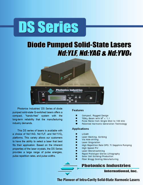
Photonics Industries’ DS Series of diode pumped solid-state Q-switched lasers offers a compact, “hands-free” system with the long-term reliability that the manufacturing industry demands.This DS series of lasers is available with a choice of Nd:YAG, Nd:YLF, and Nd:YVO4 platforms. This variety allows our customers to have the ability to select a laser that best fits their application. Based on the inherent properties of the laser crystals, the DS Series provides a large range of pulse energies, pulse repetition rates, and pulse widths. FeaturesCompact, Rugged DesignTEM00 Beam with M2 < 1.1Pulse Rates from Single Shot to 100 kHzPatented Harmonic Generation Technology ApplicationsLIDARLaser Marking, ScribingVia Hole drillingLaser SingulationHigh Repetition Rate OPO, Ti:Sapphire Pumping High Speed PIVLaser MicromachiningRapid Prototype-Stereo LithographySolar Cell Scribing/ProductionFiber Bragg Grating ManufacturingSystem ReliabilityPhotonics Industries is committed to providing a highly reliable laser to our customers. The laser resonator, which is assembled in a clean room environment, is hermetically sealed in order to prevent dust and condensation from damaging the laser crystals and optics.High PerformanceBy utilizing our end pump design, the DS Seriesdelivers superior TEM 00 beam mode quality with M 2 <1.1. Typical output performance includesPulse-to-Pulse Instability measured to be less than 1%rms. Output quality of this magnitude improvesprocess quality, control, and product yields.Low Cost of OwnershipOur DS Laser Series was designed to meet all of the laser user’s needs. The concept is to offer a laser system that will provide a cost effective solution, and go beyond the ability to achieve high power and excellent beam quality. This is exactly what has been accomplished with the DS Laser Series.The laser diode is mounted in the laser head, but outside the sealed resonator. This eliminates the fiber connection between the laser head and the controller so that they can be separated for shipment, or relocated without worry of fiber damage. The diode output is coupled to the resonator by a fiber optic cable. Since the diode package is located outside the sealed resonator, it is easily accessible for replacement by the end user without any laser alignment. The result is an adjustment-free, reliable, long lifetime operation.DS Series ControllerOur DS Series Lasers utilize a common controller unit, independent of laser model. Featuring:Single, compact, 19” Rack Mount unit User-friendly, front panel operation External control via RS-232 interface External TTL control via BNCDS Controller softwareDS10-1053 DS20-1053 DS10-527 DS20-527 Wavelength 1053 nm 1053 nm 527 nm 527 nm Average Power @ 3 kHz 7 Watts 14 Watts 6 Watts 12 Watts Pulse Width @ 1 kHz (nominal)65 ns 50 ns 50 ns 40 ns Pulse Energy @ 1 kHz4 mJ8 mJ4 mJ8 mJBeam Mode TEM 00 - M 2 < 1.1 TEM 00 - M 2 < 1.1Polarization Ratio 100:1 Horizontal100:1 Vertical Beam Diameter 1.0 mm 1.0 mm Beam Divergence <2.5 mrad <1.6 mrad Pulse-to-Pulse Instability 3% rms 3% rms Long-Term Instability 3% rms 3% rms Pointing Stability < 25 µrad< 25 µrad Pulse Repetition RateSingle shot to 10 kHz or CWSingle shot to 10 kHzDS10-351 DS20-351 DS10-263 DS20-263 Wavelength 351 nm 351 nm 263 nm 263 nm Average Power @ 3 kHz 3 Watts 7 Watts 1.5 Watts 3 Watts Pulse Width @ 1 kHz (nominal)40 ns 35 ns 30 ns 30 ns Pulse Energy @ 1 kHz2 mJ 5 mJ1 mJ2 mJ Beam Mode TEM 00 - M 2 < 1.1 TEM 00 - M 2 < 1.2 Polarization Ratio 100:1 Horizontal100:1 HorizontalBeam Diameter 0.9 mm 0.7 mm Beam Divergence <1.3 mrad <1.0 mrad Pulse-to-Pulse Instability 3% rms 3% rms Long-Term Instability 3% rms 10% rms Pointing Stability < 25 µrad < 25 mrad Pulse Repetition RateSingle shot to 10 kHzSingle shot to 10 kHzTypical DS20-527 Nd:YLF Laser Performance24681012141612345678910Repetition Rate(kHz)A v e r a g e P o w e r (W )20406080100120140160180P u l s e W i d t h (n s )Average Power @527nmPulse width @527nmDS10-1064DS20-1064DS10-532 DS20-532Wavelength1064 nm 1064 nm 532 nm 532 nm Average Power @ 10 kHz 10 Watts 20Watts 10Watts 18Watts Pulse Width @ 10 kHz (nominal)70 ns 40 ns 50 ns 40 ns Pulse Energy @ 10 kHz1 mJ 2mJ1.0 mJ 1.8mJBeam Mode TEM 00-M 2< 1.1TEM 00 - M 2< 1.1Polarization Ratio 100:1 Horizontal100:1 Vertical Beam Diameter 1.0 mm 1.0 mm Beam Divergence <2.5 mrad <1.6 mrad Pulse-to-Pulse Instability 3% rms 3% rms Long-Term Instability 3%rms 3% rms Pointing Stability < 25µrad< 25 µradPulse Repetition RateSingle shot to 50 kHz or CW Single shot to 50 kHzDS10-355DS20-355DS10-266* DS20-266*Wavelength355 nm 355 nm 266 nm 266 nm Average Power @ 10 kHz 5 Watts 10Watts 1.5 Watts 3 Watts Pulse Width @ 10 kHz (nominal)45 ns 40 ns 25 ns 25 ns Pulse Energy @ 10 kHz0.5 mJ 1mJ0.25 mJ 0.5 mJBeam Mode TEM 00-M 2< 1.1TEM 00 - M 2< 1.2Polarization Ratio 100:1 Horizontal100:1 HorizontalBeam Diameter 0.9 mm 0.7 mm Beam Divergence <1.3 mrad <1.0 mrad Pulse-to-Pulse Instability 3% rms 3% rms Long-Term Instability 3%rms 10% rms Pointing Stability < 25µrad< 25 mradPulse Repetition RateSingle shot to 50 kHzSingle shot to 50 kHz* Average Power @ 6kHz, Pulse Width @ 6kHz, Pulse Energy @ 6kHzDS20-532 Typical Performance Curve0510*******1020304050Repetition Rate(kHz)A v e r a g e P o w e r (w )20406080100120P u l s e W i d t h (n s )average power @532nmPulse width @532nmDS10H-1064 DS20HE-1064 DS10H-532 DS20H-532DS20HE-532Wavelength1064 nm 1064 nm 532 nm 532 nm 532 nm Average Power @ 40 kHz14 Watts 30 Watts 10 Watts 20 Watts 30 Watts Pulse Width @ 40 kHz (nominal)40 ns 30 ns 25 ns 25 ns 25 ns Pulse Energy @ 40 kHz0.35 mJ 0.75 mJ 0.25 mJ 0.5 mJ 0.75 mJ Beam ModeTEM 00 - M 2 < 1.1 TEM 00 - M 2 < 1.1 Polarization Ratio100:1 Horizontal 100:1 Vertical Beam Diameter1.0 mm 1.0 mm Beam Divergence<3 mrad <1.5 mrad Pulse-to-Pulse Instability3% rms 3% rms Long-Term Instability3% rms 3% rms Pointing Stability< 25 µrad < 25 µrad Pulse Repetition RateSingle shot to 150 kHz or CW Single shot to 150 kHzDS10H-355 DS20H-355DS20HE-355DS10HE-266* DS20H-266*DS20HE-266*Wavelength355 nm 355 nm 355 nm 266 nm 266 nm 266 nm Average Power @ 40 kHz5 Watts 10 Watts 15 Watts 2 Watts 4 Watts6 Watts Pulse Width @ 40 kHz (nominal)25 ns 25ns 25ns 20 ns 10 ns 10 ns Pulse Energy @ 40 kHz0.125 mJ 0.25mJ 0.375mJ 0.13 mJ 0.26 mJ 0.4 mJ Beam ModeTEM 00 - M 2 < 1.2 TEM 00 - M 2< 1.3 Polarization Ratio100:1 Horizontal 100:1 Horizontal Beam Diameter0.9 mm 0.7 mm Beam Divergence<2.5 mrad <1.0 mrad Pulse-to-Pulse Instability3% rms 3% rms Long-Term Instability3% rms 10% rms Pointing Stability< 25 µrad < 25 mrad Pulse Repetition RateSingle shot to 150 kHz Single shot to 70 kHz * Average Power @ 15kHz, Pulse Width @ 15kHz, Pulse Energy @ 15kHzNd:YVO 4 - DS20HE - 3550246810121416182030507090110130150Repetition Rate(kHz)P o w e r (W )010203040506070P u l s e W i d t h (n s )powerPulse widthC o m m o n S p e c i f i c a t i o n sInfrared, Green, and UV LasersWidth Length Height Weight Laser Head 165 mm (6.50 in) 457 mm (18.00 in) 83 mm (3.25 in)10 kg/22 lbLaser Controller 483 mm (19 in) 476 mm (18.75 in) 133 mm (5.25 in) 8 kg/17 lb Solid State Chiller 483 mm (19 in) 438 mm (17.24 in) 177 mm (7.0 in) 20 kg/43 lb Electrical Requirement 110 VAC 20 Amps or 220 VAC 10 Amps @ 50/60 HzAmbient Temperature 15 to 30 o C (59 to 86 o F) Operating RangeHumidity Non-CondensingUmbilical Length 3 meters (10 feet)Infrared, Green, and UV Lasers HeadLasers Head ControllerDeep UV LasersWidth Length Height Weight Laser Head 203 mm (8.00 in) 711 mm (28.0 in) 152.0 mm (6.0 in) -- Laser Controller 483 mm (19 in) 476 mm (18.75 in) 133 mm (5.25 in) 17 kg/37 lb Solid State Chiller 483 mm (19 in) 438 mm (17.24 in) 177 mm (7.0 in) 20 kg/43 lb Electrical Requirement 110 VAC 20 Amps or 220 VAC 10 Amps @ 50/60 HzAmbient Temperature 15 to 30 o C (59 to 86 o F) Operating RangeHumidity Non-CondensingUmbilical Length 3 meters (10 feet)Deep UV Lasers HeadIn order to continuously improve our products, we reserve the right to change all specification with out prior notice.Please contact the factory for the most recent dimensions.Optional FeaturesPower Attenuator: This patented feature allows laser output power to be controlled by either manual adjustment, or by computer control via RS232. The laser output power can be controlled from approximately 1% to 98% of the maximum available power.Beam Expander: Please contact us for details on all DS series laser accessories and optional features.Customized ProductsIn addition to our standard laser specifications, customized versions can be provided to meet our customer’s specific requirements including; long or short pulse duration and Single Longitudinal Mode (SLM). For higher average power, please contact us for the availability of our PA series lasers.WARRANTYPhotonics Industries International, Inc. offers a limited warranty for all DS Series laser systems. All components and assemblies are guaranteed to be free of defects in materials and workmanship for the duration of the warranty period. Please contact our sales office, or visit our website for complete details on our standard and extended warranty coverage.Due to Photonics Industries’ commitment to continuous product improvement,Specifications are subject to change without notice.。
GaN光致发光谱与穿透位错特性解析
[1].陆敏,方慧智,陆曙,黎子兰.腐蚀坑处氮化镓二次MOCVD外延生长的特性[J].半导体学报, 2004,(04)
[2].李伟,赵智彪,郑燕兰,李存才.RF Plasma MBE生长GaN材料及特性研究[J].功能材料与器件学报, 1999,(03)
[3].王三胜,顾彪,徐茵,徐久军.ECR-PEMOCVD法在GaAs(001)衬底上制备GaN量子点[J].半导体光电, 2002,(02)
[4].蒋建国.电子显微技术的现状与发展[J].扬州教学院学报, 2003,(03)
[5].袁小武,肖定全,朱基亮,方瑜.Sol-gel制备PLCT薄膜的结晶特性与电畴结构研究[J].功能材料, 2005,(07)
[6].宋登元,王秀山.GaN材料系列的研究进展[J].微电子学, 1998,(02)
GaN
氮化镓(GaN)是宽禁带直接带隙半导体材料,具有优良的光学和电学性质,在蓝绿到紫外波段的光电子器件和高功率微波器件等领域有着广泛的应用前景。在GaN基光电子器件中,材料中的缺陷和杂质所产生的深能级发光会降低带间辐射复合跃迁的发光效率。在众多有关GaN薄膜光致发光(PL)特性研究的报道中,不同的样品所测的光致发光谱不尽相同,特别是对GaN半导体材料深能级发光的起源,不同文献的解释存在争议。因此,进一步研究GaN的光致发光谱是必要的。本文采用四种不同光源作为激发光源,实验研究了金属有机物汽相外延方法(MOVPE)在蓝宝石衬底上生长的GaN的光致发光光谱特性。结果发现采用氙灯光源和He-Cd激光器两种连续光作为激发光源时,PL谱中均出现较宽的黄带发光,其中心波长位于550nm附近。而采用YAG激光器和He-Cd激光器两种脉冲光作激发光源时,PL谱中主要出现中心波长位于约365nm的带边发光峰,而未出现黄带发光。结果表明蓝宝石衬底上MOVPE生长GaN薄膜的PL谱中黄带发光特性与激发光源性质有关。这对于进一步研究深能级的起源有一定的参考价值。GaN的深能级发光特别是黄带发光与材料的本生位错缺陷直接相关。GaN通常在蓝宝石衬底上异质外延生长,然而蓝宝石异质外延衬底与GaN之间存在较大的晶格失配,导致GaN外延层中的位错缺陷密度高达108-1010cm-2。延伸到GaN表面的穿透位错(TDs)会形成非辐射复合中心和光散射中心,降低光电子器件发光效率。有文献报道只有纯螺型TDs和混合型TDs才是非辐射复合中心,也有报道部分纯刃型TDs对非平衡少数载流子有一定的非辐射复合作用。总之,人们对穿透位错类型与非辐射复合中心的对应关系尚无统一的认识。因此,研究GaN的穿透位错特性将有助于揭示其深能级发光机理。本论文采用原子力显微镜(AFM)同位观测方法,对MOCVD生长GaN样品标记区域进行表面形貌测试,统计得到每个位错坑的半径和深度在腐蚀前和2次腐蚀后的变化,并根据位错坑的初始位置,结构和腐蚀速率判定各位错对应的类型。结果发现,热磷酸腐蚀后位错坑的半径和深度存在一定对应关系,其中半径大的腐蚀坑的深度也较大,而半径小的腐蚀坑的深度也较小。按半径和深度大小可分为大坑和小坑两类,这两类所占的百分比分别为52.7%和47.3%。小坑在腐蚀前位于GaN自然生长面的台阶面上,为刃位错,而大坑在腐蚀前位于台阶终结处,为混合位错或螺位错。位错坑结构腐蚀前后同位跟踪分析还发现,位错坑的结构随着腐蚀时间而变化,这意味着位错坑结构与位错类型不存在一一对应关系。另外,实验数据显示两种位错坑半径的腐蚀速率几乎都是其深度腐蚀速率的10倍左右,说明GaN在热磷酸腐蚀时的横向腐蚀速率大于其纵向腐蚀速率,这解释了实验观察到的刃位错形成的小腐蚀坑在长时间腐蚀后,因超出AFM所能分辨的范围而“消失”的现象。把80分钟腐蚀后GaN样品的阴极荧光(CL)全色显微图像与扫描电镜(SEM)在同一微区获得的显微图像进行对比分析,分析发现SEM得到的80分钟腐蚀样品的腐蚀坑密度与AFM结果一致,然而CL显微图像中非辐射复合中心密度是这一腐蚀坑密度的2倍。这说明经过80分钟腐蚀后,占样品总位错密度一半的刃位错在AFM和SEM下几乎全部“消失”,但作为穿透位错,刃位错实际仍然存在于样品中,因此在CL显微图像中仍然能观测到这部分刃位错,也说明刃位错和带有螺分量的位错均是非辐射复合中心。这为进一步深入研究单个不同类型位错区域的发光特性奠定了基础。
激光剥离技术制备GaN/metal/Si的结构和光学特性研究
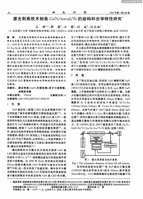
将生 长在蓝 宝石衬底 上 的 G N 外 延层 转 移 到 S 衬 底 a i 上 。G N 和 S 表 面 分 别 用 电子 束 蒸 发 A1T / a i / iAu和 TiAu I / /n后 , 氮 气环 境 下 2 0 在 0 ℃加 压 实现 G N和 S a i
Ga AlT / /n Au TiS 结构 , 图 1所示 。 N/ / iAu I / / / i 如
应用促 进 了研 发 和 商用 器 件 方 面 的 快 速 发展 [z。 由 1] . 于 自然界 缺乏天 然 Ga 单 晶 , N 目前 Ga 基 L D一 般 N E
是异 质外 延在与 之 晶系结 构相 容的 蓝 宝石 衬底 上 。但
的键 合 。 采 用脉 冲 宽 度 3 n 、 长 2 8 m 的 准 分 子 脉 0 s波 4n
冲激光 透过蓝 宝石衬 底辐 照 G N 薄膜 , 脉 冲激 光 能 a 在
量 密度 为 3 0 / m。的 条 件 下 将 蓝 宝 石 衬 底 剥 离 下 8 mJ e
合 。衬 底转移 后样 品 的截面 扫描 电镜 ( E 照片说 明 S M) 形 成 了 致 密 的 G N A1TiAu I/ / iS 结 构 。 a / / / /n Au T / i
关键 词 : 激光 剥 离 ; N; 描 电镜 ; 子 力 显微 镜 ; Ga 扫 原 光致发 光谱 中图分类号 : TN3 2 1 文献 标识码 : A
文章 编号 :0 19 3 (0 7 0 0 80 1 0 -7 1 2 0 ) 卜0 8 —3
1 引 言
G N基 发光 二极 管 ( E 在 众 多 领 域 中的 广 泛 a L D)Βιβλιοθήκη 利影 响 。 2 实 验
Si衬底上外延生长GaN基射频电子材料的研究进展
冲层 [2-4] 、Al 组分梯度渐变 AlGaN 缓冲层 [5-6] 等方法,已能初步满足低阻 Si 衬底上 GaN 基功率电子器件对材
料的要求;然而目前高阻 Si 衬底上 GaN 及其异质结构材料仍然存在很高的位错密度,其应力 / 翘曲控制仍然
困难,严重影响器件的性能及可靠性。
此外,尽管采用高阻 Si 衬底,射频损耗仍然是阻碍 Si 衬底上 GaN 基射频电子材料和器件发展的关键瓶
颈。 其内涵是 Si 衬底上 GaN 基射频器件在信号传输时存在传输的损耗,这会造成信号精准性和器件工作效
率的下降。 Si 衬底上 GaN 基射频器件的射频损耗主要包括 4 个部分 [7] :1) 导体损耗,也可称为传输线损耗。
YANG Xuelin1,2,3 , SHEN Bo1,2,3,4
(1. Research Center for Wide Gap Semiconductors, Peking University, Beijing 100871, China;
2. State Key Laboratory of Artificial Microstructure and Microscopic Physics, Peking University, Beijing 100871, China;
这部分损耗主要与选择的传输线结构、几何尺寸、金属材料及工艺等因素相关,可以通过相对应的工艺优化
进行解决。 2) 衬底损耗。 这部分损耗可以通过使用高阻的 Si 衬底进行解决。 3) 由于 Si 衬底和半导体界面
的导电层带来的界面损耗。 4) 无法避免的辐射损耗,这部分损耗通常可以忽略不计,只在严重失配或者特
基于光子晶体光纤的法布里-珀罗干涉传感器
万方数据电子科技大学学报第38卷etc.,havebeensuccessfullycommercializedandwidelyusedforhealthmonitoringofcompositematerials,largecivilengineeringstructures(e.g.bridgesanddams),spaceaircrafts,andairplanes,etc.,whichwouldleadtotherealizationofSO.calledsmartmaterialsandstructures,andharshenvironments(e.g.hightemperature).WiththegenerationofPCFs,therearepossibilitiesthatbyincorporatingPCFsintotheFFPIstructure,fundamentalprogresscouldbemadetowardsthesignificantenhancementinfunctionalityandreliabilityofFFPIsensors,offeringagreatpotentialtoformanewgenerationofFFPIsensors.Fig.1ConfigurationoftypicalFFPIsensor(extrinsicFFPD2FFPIFormedByHollowCorePCF2.1SensorFabricationandCharacteristicsAtypicalFFPIsensorbasedonconventionalfibersisshowninFig.1,wheretheF-Pcavityisnormallyformedbyahollowglasstube.Duetotheveryhighlossoftheglasstubeasawaveguide,thecavitylengthislimitedtobequiteshort,usuallylessthanafewhundredmicrometers,makingthefabricationandassemblyofthesensordifficulttocontrol,resultingrelativelypoorrepeatability.Bycontrast,hollow—corephotonicbandgapfibersuseamicrostructuredcladdingregionwithairholestoguidelightinahollowcore.Thephotonicbandgapguidingmechanismisfundamentallydifferentfromthetraditionaltotalinternalreflectionguidingprinciple.TheHCPCF—FFPIisconstructedbysplicingasectionofhollow-corePCF(HCPCF)betweentwostandardsingle-modefibers(ComingSMF-28)toformallin-lineetalon,as‘displayedinFig.2and3【,j.Such.anin—lineHCPCFetaloncangreatlyenhancethemultiplexingcapabilitywithspatialdivisionmultiplexing(SFDM)duetothesubstantialincreaseinthecavitylength.Inthiswork,thefringevisibilityVismainlydeterminedbythesplicinglossbetweenthesingle.modefiberandtheHCPCFastheverylOWtransmissionlossoftheHCPCFCanbeignored,ratherthanthecavitylengthinaconventionalF-Pcavitywithallairgap.Hence,Vvarieslittlewiththecavitylength.WhichisverifiedbyoHrexperimentevenwhentheHCPCHetalonlengthiSextendedto2cm.Ontheotherhand,VisenhancedgreatlybycoatingthereflectivefiberendwithahJighreflectionfilm,asshowninFig.4.Fig.2Configurationofin—lineHCPCFetalon五/nm乱withoutreflectivefilmA/nmb.withreflectivefilmFig.4ReflectivesignalsfromaHCPCHetalon 万方数据 万方数据490电予科技大学学报第38卷speedsatthewavelengthof1550衄.Fig。
激光冲击强化应变率
激光冲击强化应变率
激光冲击强化应变率(Laser Shock Peening, LSP)是一种利用
激光脉冲瞬时作用在金属表面的强化加工技术,通过在材料表面产生高压冲击波,从而引起材料的塑性应变和冷变形,提高材料的耐久性能。
激光冲击强化应变率的过程主要包括以下几个步骤:首先,利用激光器将高能量的激光束聚焦到小面积的金属表面上,产生高温、高压的等离子体。
然后,在激光作用下的等离子体区域中产生激波,并通过激波的作用力使金属表面发生弹性变形和塑性变形。
最后,随着激波的传播和衰减,金属表面的形变会逐渐减小,形成残余应变。
激光冲击强化应变率可以显著提高材料的机械性能和疲劳寿命,包括增加材料的硬度、抗疲劳性能、抗腐蚀性能和抗应力腐蚀性能。
此外,它还可以改善材料的表面质量和加工精度,减少材料的残余应力和变形。
因此,激光冲击强化应变率广泛应用于航空航天、汽车、电子、船舶等领域的高强度、耐磨材料的表面处理和强化改性。
新方法领域带来新型光纤

新方法领域带来新型光纤
北极星电力软件网讯:近日麻省理工学院的研究人员发现了一种新的方法来捕捉光线,可以带来各种各样的应用。
研究人员说,该方法的应用领域可能包括大尺度激光器和化学生物传感器。
许多光学器件都需要这种结构,包括激光器、光伏电池、光纤。
光发现被局限在一个平面介质光子晶体。
光子晶体中以灰色显示,红色和蓝色的颜色表示此被困的光的状态的平面外的电场密度。
Chia Wei Hsu 光被局限在一个平面介质光子晶体。
光子晶体显示淡蓝色,深蓝色表面的电磁能量密度,此为被约束光的状态。
Bo Zhen
有许多方法可以捕捉光通常使用镜子和反射表面,或者像光学晶体之类的高科技材料。
然而近日麻省理工学院的研究人员发现了一种新的方法来捕捉光线,可以带来各种各样的应用。
该发现发表在《自然》杂志上。
这种新方法利用光波限制光波:两个光波的波长相同,但相位相反,当一个光波在波峰时,另一个在波谷。
通过这种方法,光波相互抵消。
同时其他波长(颜色)的光波可以透过。
研究者首先通过数值模拟预言这一现象的存在,然后在实验中验证了这个设想。
研究人员说,这种设计可以适用于任何类型的波:声波,无线电波,电子(其行为用波函数描述),甚至是海浪。
许多光学器件都需要这种结构,Solja?i?说道,包括激光器、光伏电池、光纤。
限制光波的方法通常使用各种镜子,包括传统镜子和更先进的介质镜,也有奇异的光学介质。
在这些情况下,光的通道全部被限制:有没有允许状态的光波继续在其路径上,因此它被强制反射。
第五讲 激光冲击加工

Postgraduate
激光冲击加工原理
Postgraduate
激光冲击加工参数要求
1、作用于单位面积金属上峰值功率密度要求: GW/cm2 2、持续时间要求:10-30ns 3、为保证加工效率:重复频率,>1~10Hz
Postgraduate
激光器参数要求 参数 能量 ~30J 脉宽 10-30ns 频率 ≥3HZ 光斑 3-5mm
Postgraduate
江大 能量 频率 35J 单次
MIC ≥25J ≥3HZ
THALES >13J 10HZ
脉宽
工作介质 SBS系统
22ns
Nd:glass棒 无
20ns
板条Nd:glass 有
<15ns
陶瓷板条YAG 有
中继望远系统
泵浦 传播方式 冷却液
无
氙灯 直线 水
有
氙灯 Z字形 水
有
氙灯 Z字形 水
Postgraduate
请思考脉冲激光器输出脉冲的脉冲宽度 由什么因素决定?
YAG
自由振荡激光器
透反镜 氙灯 全反镜
YAG
调Q激光器
透反镜 氙灯 偏振器 KDP晶体 全反镜
Postgraduate
推导激光振荡器阈值条件
R1 R2
全反射镜 L
输出
部分反射镜R1、R2 左、右两反射镜的反射率.对照上表,可见江苏大学激光冲击强化设备的 不足之处。
Postgraduate
MIC公司
MIC公司和美国利弗莫尔实验室合作开发了一台 目前已经用于实用化的激光系统,具体参数如下: 能量 脉宽 频率 光斑 ≥25J 10-100ns ≥5HZ 5×5mm
Postgraduate
SPI-SPE_抛光标准

SPI-SPE_抛光标准
拋光標准
一. 試模前必須檢查打光是否完全符合要求或是否全部完成.<br> 二. 火花紋地方是否正确及是否可以出模.<br>
三. 所有鏡面打光,鋼材必須用ASSAB 136,見硬52-54HKC工件表面光洁度按照下列新標准
SPI-SPE 工件表面光洁度標准
A-0 #1鑽石膏(光學要求)
A-1 #3鑽石膏拋光(鏡面)
A-2 #6鑽石膏拋光(鏡面)
A-3 #15鑽石膏拋光(鏡面)
B-1 600 沙紙(光面)
B-2 400 沙紙(光面)
B-3 320 沙紙(光面)
C-1 600 沙紙(光面)
C-2 400 油石(啞面)
C-3 320 沙紙(光面)
D-1 噴#11粗玻璃珠
D-2 噴#240沙
D-3 噴#24沙
1. 見硬方法
- 用真空熱處理.
- 見硬時在熱處理通知表必須注明:
1. 德勝2083ESR
2. 硬度52-54HRC
3. 高溫淬火+2次低溫回火
4. 大陸的加工厂可以在德勝熱處理;香港加工厂可以繼續用好百利.
1. 加工方法
用EDM火花電蝕加工,但需注意以下几點:
- 用低電流加工.因為高電流粗加工容易留下凹穴,打光時留下深孔. - EDM只适用日本火花机加工,因台灣机火花紋深淺不一,會留下深孔.以因拋光鑽石膏后才看到 "孔",如有凹孔重新打光需由#320開始,會浪費大量工時.。
- 1、下载文档前请自行甄别文档内容的完整性,平台不提供额外的编辑、内容补充、找答案等附加服务。
- 2、"仅部分预览"的文档,不可在线预览部分如存在完整性等问题,可反馈申请退款(可完整预览的文档不适用该条件!)。
- 3、如文档侵犯您的权益,请联系客服反馈,我们会尽快为您处理(人工客服工作时间:9:00-18:30)。
and 2 tm thick, respectively.
*Email: jan.j.dubowskinrc.ca
442 Laser Applications in Microelectronic and Optoelectronic Manufacturing VI, Malcolm C. Gower, Henry Helvajian, Koji Sugioka, Jan J. Dubowski, Editors, Proceedings of SPIE Vol. 4274 (2001) © 2001 SPIE · 0277-786X/01/$15.00
பைடு நூலகம்
2. EXPERIMENTAL DETAILS
The GaN layers were grown on (0001) sapphire substrates in a custom built ammonia-molecular beam epitaxy system
[5]. The initial buffer/nucleation layer of A1N was grown by magnetron sputter epitaxy. The A1N and GaN layers were 20 nm
Samples were irradiated at normal incidence with 10 ns pulses from a XeCl excimer laser (X 308 nm) using an experimental setup described elsewhere [6]. The irradiation was carried out with laser pulse fluences between 99 - 231 mJ/cm2. The experiment was carried out in an air environment. The diameter of laser etched craters was about 375 tm. Following laser irradiation, the samples were etched in a 50% solution of HC1/H20 to remove excessive Ga formed at the irradiated surface. The ablation rate was determined from direct measurements of the depth of laser-produced craters by
Due to its attractive properties, gallium nitride (GaN) has received in recent years a steadily growing attention by fundamental and applied research communities. The interest is primarily driven by the potential this material has for the development of blue-emitting laser diodes and high-frequency, high-power devices. The rapid expansion of this material into optoelectronic application is, however, significantly hindered by the lack of large size lattice matched substrates. Sapphire (Al203) remains to be the most popular substrate applied for the hetero-epitaxial growth of this material. The growth has also been investigated on other substrates, such as SiC, Si, GaAs, MgO, ZnO [1]. A significant lattice mismatch between GaN and sapphire complicates the growth of a high quality (low-defect) material. It contributes to the increased surface roughness of GaN films and may result in, for instance, a reduced capability of high-definition patterning of such material. Consequently, a method improving smoothness of hetero-epitaxially grown GaN through the post-growth treatment has a potential practical application. Some recent investigations have indicated that such a process is feasible through the laser-induced thermal decomposition of the GaN surface. It has been demonstrated that the irradiation with several pulses of a KrF [2,3] and a F2 [4] lasers could lead to a significant planarization of GaN films grown on sapphire. The maximum effect, a reduction from the initial roughness of 0s = 1 0 nm to 2 nm, was observed for the 7-pulse KrF laser irradiation at the fluence of F 1 J/cm2 per pulse (i; = 34 ns) [3]. It is well known however that the laser interaction with solid surfaces at such high laser fluence can easily induce significant damage to the processed material. Clearly, the attractiveness of the laser-induced planarization process of GaN will depend on the ability to carry it out without inducing significant damage, or to confine the laser-induced damage to as small volume as possible. One possible route to achieve that would be by the application of a shorter wavelength laser, such as F2 (157 nm), as has been reported recently [4]. Short-pulse ablation, with a laser operating in the
Laser polishing of GaN
J.J. Dubowski*, S. Moisa, B. Komorowski, H. Tang and J.B. Webb Institute for Microstructural Sciences, National Research Council of Canada, Ottawa, Ontario K1A 0R6, Canada
ABSTRACT
The ablative decomposition of GaN films induced with a XeC1 excimer laser (? = 308 nm) was investigated for a potentially low-damage surface planarization process. Samples, 2-tm-thick, were grown on (0001) sapphire by ammonia molecular beam epitaxy. They had a characteristic micro-hillock type surface morphology with a roughness, averaged over 5 x 5 tm2 area, typically, of 13 nm. Following the laser irradiation, this roughness could be reduced to 3.6 urn. The results indicate that the ablation process follows the Lambert-Beer's law, with an absorption coefficient of 3 x iO cm'. The experiment was carried out with relatively short pulses ('r = 10 ns), which appear to be responsible for the observed onset of the laser-induced decomposition of GaN and surface planarization at significantly smaller laser fluences than reported in the literature. The ability to carry out decomposition of GaN with low laser fluences is of practical importance for achieving a low-damage GaN planarization process and/or intentional delaminating of this material from the sapphire substrate by the back side irradiation technique.