IXGH12N60CD1;中文规格书,Datasheet资料
TC12-11YWA, 规格书,Datasheet 资料
Electrical / Optical Characteristics at TA=25°C
Symbol λpeak λD [1] Δλ1/2 C VF [2] IR Parameter Peak Wavelength Dominant Wavelength Spectral Line Half-width Capacitance Forward Voltage Reverse Current Device Yellow Yellow Yellow Yellow Yellow Yellow Typ. 590 588 35 20 2.1 2.5 10 Max. Units nm nm nm pF V uA Test Conditions IF=20mA IF=20mA IF=20mA VF=0V;f=1MHz IF=20mA VR=5V
REV NO: V.10 CHECKED: Joe Lee
DATE: APR/02/2011 DRAWN: J.Yu
PAGE: 3 OF 6 ERP: 1332000511
芯天下--/
PACKING & LABEL SPECIFICATIONS
TC12-11YWA
SPEC NO: DSAC4401 APPROVED: WYNEC
30.6mm (1.2 INCH) 5x7 DOT MATRIX DISPLAY
Part Number: TC12-11YWA Yellow
Features
1.2 inch matrix height. Dot size 3mm. Low current operation. High contrast and light output. Column cathode and column anode available. Easy mounting on P.C. boards or sockets. Mechanically rugged. Standard : gray face, white dot. RoHS compliant.
IXGH17N100A;IXGH17N100;中文规格书,Datasheet资料
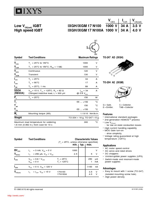
© 1996 IXYS All rights reservedSymbol Test Conditions Maximum RatingsV CES T J = 25°C to 150°C1000V V CGR T J = 25°C to 150°C; R GE = 1 M Ω1000V V GES Continuous ±20V V GEM Transient ±30V I C25T C = 25°C 34A I C90T C = 90°C 17A I CMT C = 25°C, 1 ms68A SSOA V GE = 15 V, T VJ = 125°C, R G = 82 Ω I CM = 34A (RBSOA)Clamped inductive load, L = 300 µH @ 0.8 V CESP C T C = 25°C150W T J -55 ... +150°C T JM 150°C T stg -55 ... +150°CM d Mounting torque (M3) 1.13/10Nm/lb.in.WeightTO-204 = 18 g, TO-247 = 6 gMaximum lead temperature for soldering 300°C1.6 mm (0.062 in.) from case for 10 sSymbol Test ConditionsCharacteristic Values(T J = 25°C, unless otherwise specified)min.typ.max.BV CES I C = 3 mA, V GE = 0 V 1000V V GE(th)I C= 250 µA, V CE = V GE2.55V I CES V CE = 0.8 • V CES T J = 25°C 250µA V GE = 0 VTJ = 125°C1mA I GES V CE = 0 V, V GE = ±20 V ±100nA V CE(sat)I C= I C90, V GE = 15 V17N100 3.5V 17N100A4.0VTO-247 AD (IXGH)V CESI C25V CE(sat)Low V CE(sat) IGBT IXGH/IXGM 17 N1001000 V 34 A 3.5 V High speed IGBTIXGH/IXGM 17 N100A 1000 V 34 A4.0 VGCETO-204 AE (IXGM)CG = Gate, C = Collector,E = Emitter,TAB = CollectorFeaturesl International standard packages l 2nd generation HDMOS TM process l Low V CE(sat)-for low on-state conduction losses l High current handling capability l MOS Gate turn-on -drive simplicitylVoltage rating guaranteed at high temperature (125°C)Applicationsl AC motor speed control l DC servo and robot drives l DC choppersl Uninterruptible power supplies (UPS)lSwitch-mode and resonant-mode power suppliesAdvantageslEasy to mount with 1 screw (TO-247)(isolated mounting screw hole)lHigh power density91515E (3/96)IXYS MOSFETS and IGBTs are covered by one or more of the following U.S. patents:4,835,5924,881,1065,017,5085,049,9615,187,1175,486,7154,850,0724,931,8445,034,7965,063,3075,237,4815,381,025IXYS reserves the right to change limits, test conditions, and dimensions.SymbolTest ConditionsCharacteristic Values(TJ = 25°C, unless otherwise specified)min.typ.max.g fs I C = I C90; V CE = 10 V,615S Pulse test, t ≤ 300 µs, duty cycle ≤ 2 %C ies 1500pF C oes V CE = 25 V, V GE = 0 V, f = 1 MHz175pF C res 40pF Q g 100120nC Q ge I C = I C90, V GE = 15 V, V CE = 0.5 V CES 2030nC Q gc 6090nC t d(on)100ns t ri 200ns t d(off)5001000ns t fi 17N100750ns 17N100A 450750ns E off 17N100A3mJ t d(on)100ns t ri 200ns E on 2.5mJ t d(off)7001000ns t fi 17N10012002000ns 17N100A 7501000ns E off 17N1008mJ 17N100A 6mJR thJC 0.83K/WR thCK0.25K/WIXGH 17N100 and IXGH 17N100 A characteristic curves are located on the IXGH 17N100U1 and IXGH 17N100AU1 data sheets.Inductive load, T J = 25°C I C = I C90, V GE = 15 V, L = 300 µH,V CE = 0.8 V CES , R G = R off = 82 ΩRemarks: Switching times may increasefor V CE (Clamp) > 0.8 • V CES ,higher T J or increased R G Inductive load, T J = 125°C I C = I C90, V GE = 15 V, L = 300 µH V CE = 0.8 V CES , R G = R off = 82 ΩRemarks: Switching times may increasefor V CE (Clamp) > 0.8 • V CES ,higher T J or increased R G分销商库存信息:IXYSIXGH17N100A IXGH17N100。
IXGX120N60B3;中文规格书,Datasheet资料
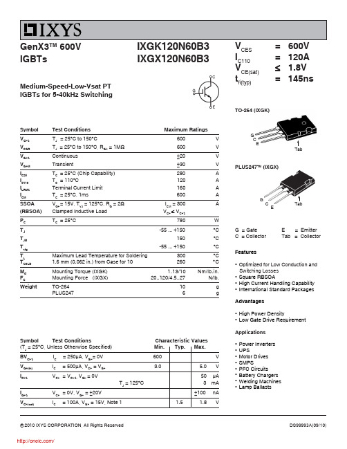
© 2010 IXYS CORPORATION, All Rights Reserved GenX3TM 600V IGBTsDS99993A(09/10)V CES = 600V I C110= 120A V CE(sat)≤ 1.8V t fi(typ)= 145nsMedium-Speed-Low-Vsat PT IGBTs for 5-40kHz SwitchingIXGK120N60B3IXGX120N60B3Symbol Test Conditions Characteristic Values (T J = 25°C, Unless Otherwise Specified ) Min. Typ. Max.BV CES I C = 250μA, V GE = 0V 600 VV GE(th)I C= 500μA, V CE = V GE3.05.0VI CES V CE = V CES , V GE = 0V50μA T J = 125°C 3 mA I GES V CE = 0V, V GE = ±20V ±100 nAV CE(sat)I C= 100A, V GE = 15V, Note 1 1.5 1.8 VSymbol Test Conditions Maximum RatingsV CES T J = 25°C to 150°C600 V V CGR T J = 25°C to 150°C, R GE = 1M Ω600 V V GES Continuous ±20 V V GEM Transient±30 VI C25T C = 25°C (Chip Capability)280 A I C110T C = 110°C 120 A I LRMS Terminal Current Limit 160 A I CMT C = 25°C, 1ms 600 A SSOA V GE = 15V, T VJ = 125°C, R G = 2Ω I CM = 300 A (RBSOA)Clamped Inductive Load V CE ≤ V CESP C T C = 25°C780 WT J -55 ... +150 °C T JM 150 °C T stg -55 ... +150 °CT LMaximum Lead Temperature for Soldering 300 °C T SOLD 1.6 mm (0.062 in.) from Case for 10 260 °C M d Mounting Torque(IXGK) 1.13/10 Nm/lb.in.F C Mounting Force (IXGX)20..120/4.5..27 N/lb.WeightTO-26410 g PLUS2476 gFeatureszOptimized for Low Conduction and Switching Losses zSquare RBSOA zHigh Current Handling Capability zInternational Standard PackagesAdvantagesz High Power DensityzLow Gate Drive RequirementApplicationsz Power Inverters z UPSz Motor Drives z SMPSz PFC Circuits z Battery Chargers z Welding Machines zLamp BallastsG = GateE = Emitter C = Collector Tab = CollectorTabTO-264 (IXGK)EC Tab6,727,5857,005,734 B2 7,157,338B2by one or moreof the following U.S. patents:4,850,0725,017,5085,063,3075,381,0256,259,123 B16,534,3436,710,405 B26,759,6927,063,975 B24,881,1065,034,7965,187,1175,486,7156,306,728 B16,583,5056,710,4636,771,478 B27,071,537Dim.Millimeter InchesMin.Max.Min.Max.A 4.82 5.13.190.202A1 2.54 2.89.100.114A2 2.00 2.10.079.083b 1.12 1.42.044.056b1 2.39 2.69.094.106b2 2.90 3.09.114.122c 0.530.83.021.033D 25.9126.16 1.020 1.030E 19.8119.96.780.786e 5.46 BSC .215 BSC J 0.000.25.000.010K 0.000.25.000.010L 20.3220.83.800.820L1 2.29 2.59.090.102P 3.17 3.66.125.144Q 6.07 6.27.239.247Q18.388.69.330.342R 3.81 4.32.150.170R1 1.78 2.29.070.090S 6.04 6.30.238.248T 1.57 1.83.062.072Terminals:1 - Gate2 - Collector3 - EmitterPLUS247TM (IXGX) Outlinelimeter Inches Min.Max.Min.Max.A 4.83 5.21.190.205A 1 2.29 2.54.090.100A 2 1.91 2.16.075.085b 1.14 1.40.045.055b 1 1.91 2.13.075.084b 2 2.923.12.115.123C 0.610.80.024.031D 20.8021.34.819.840E 15.7516.13.620.635e 5.45 BSC .215 BSC L 19.8120.32.780.800L1 3.81 4.32.150.170Q 5.59 6.20.2200.244R4.32 4.83.170.190Terminals: 1 = Gate2,4 = Collector3 = EmitterBack SideIXYS Reserves the Right to Change Limits, Test Conditions, and Dimensions.IXYS Reserves the Right to Change Limits, Test Conditions, and Dimensions.分销商库存信息: IXYSIXGX120N60B3。
LG iGX样本(中文版)
-Solution Leader in Electrics& Automation
STARVERT G X
紧凑高性能变频器
0.4~22kW 3Phase 380~480Volts
Automatiom Equipment
New Name of
小心选择电流断路器. 当变频器上电的时候,可能有大 的浪涌电流涌入
为了使变频器长时间运行在高性能状态下,请把变频器安 装在正确的方向的适当的位置,留出适当的空间.不正确的 端子接线会导致设备的损坏.
有必要的情况下再安装。 如果安装了,不要用它来 启动和停止变频器。否则, 容易缩短产品的使用寿命。
控制连线
安全警告
为了您的安全,请在操作前先阅读说明书 请联系授权的服务人员进行检查、维修、调整 请由专业人员进行拆除维修
LS产电的30年
LS产电在不断地变革和成长中积累了丰富的经验。 同时具备了面临激烈竞争及挑战时也能生存并发展的强大组织力量。
取得飞跃和成长的企业 1974年 金星机电(株)创立 1987年 金星产电(株)设立 1994年 企业上市
电气及自动化领域的领先者 1995年 商号变更为LG产电(株) 1996年 取得了韩国最早变频器领域
的ISO9001认证 1998年 低压电器生产突破1亿台
第二次质的飞跃 1999年 合并LG金属(株) 1999年 转让铜管和自动销售机事业 2003年 内部调整,归属于LG电缆 2005年 更名为LS产电
动能缓冲
电源突降或瞬时掉电的情况下,变频器会出现欠压故障并保护停机。使 用此功能后,变频器在电源出现问题时会根据减速方式或直流电压参考方式 控制输出频率,利用电机产生的回馈能量维持直流侧电压以延长出现欠压保 护的时间,实现电源突降或瞬时掉电的情况下变频器能持续工作。
DSEI12-12A;中文规格书,Datasheet资料

007 004IXYS reserves the right to change limits, test conditions and dimensions.Symbol Conditions Characteristic Valuestyp.max.I RV R = V RRM T VJ = 25°CV R = 0.8·V RRM T VJ = 25°C V R = 0.8·V RRM T VJ = 25°C 250 504µA µA mA V F I F = 2 A T VJ = 50°CT VJ = 25°C2.22.6V V V T0r T For power-loss calculations only T VJ = T VJM.6546.2V m W R thJC R thCH R thJA 0.5.660K/W K/W K/W t rr I F = A; -di/dt = 50 A/µs; V R = 30 V; T VJ = 25°C 5070ns I RMV R = 540 V; I F = 2 A; -di F /dt = 00 A/µs L < 0.05 µH; T VJ = 00°C6.57.2AI FAVM rating includes reverse blocking losses at T VJM . V R = 0.8·V RRM , duty cycle d = 0.5Data according to IEC 60747I FAV = 11 A V RRM = 1200 V t rr = 50 n sFast RecoveryEpitaxial Diode (FRED)Features• International standard package JEDEC TO-220 AC• Planar passivated chips • Very short recovery time• Extremely low switching losses • Low I RM -values• Soft recovery behaviour • Epoxy meets UL 94V-0Applications• Antiparallel diode for high frequency switching devices • Anti saturation diode • Snubber diode• Free wheeling diode in converters and motor control circuits• Rectifiers in switch mode power supplies (SMPS)• Inductive heating and melting• Uninterruptible power supplies (UPS)• Ultrasonic cleaners and welders Advantages• High reliability circuit operation • Low voltage peaks for reduced protection circuits • Low noise switching • Low losses• Operating at lower temperature or space saving by reduced coolingSymbol ConditionsMaximum RatingsI FRMS I FAVM I FRM T VJ = T VJMT C = 00°C; rectangular, d = 0.5t p < 0 µs; rep. rating, pulse width limited by T VJM 25 50A A A I FSMT VJ = 45°C; t = 0 ms (50 Hz), sinet = 8.3 ms (60 Hz), sine7580A T VJ = 50°C; t = 0 ms (50 Hz), sine t = 8.3 ms (60 Hz), sine6570A I 2tT VJ = 45°C; t = 0 ms (50 Hz), sinet = 8.3 ms (60 Hz), sine2827A 2s T VJ = 50°C; t = 0 ms (50 Hz), sine t = 8.3 ms (60 Hz), sine2 20A 2s T VJT VJM T stg -40...+ 5050-40...+ 50°C °C °C P tot T C = 25°C 78W M d mounting torque 0.4...0.6Nm Weight typical 2gA CTO-220 A CA = Anode, C = CathodeCC AV RSM V V RRM V Type12001200DSEI 12-12A007 004IXYS reserves the right to change limits, test conditions and dimensions.10030002004000.00.20.40.60.81.00.0010.010.11100.00.40.81.21.62.0040801201600.20.40.60.81.01.21.4K fT VJ [°C]-di F /dt [A/µs]t [s]100200300400102030405060020040060080010001200VF R [V ]di F/dt [A/µs]100300020040051525010203011010010000.00.51.01.52.02.53.00123102030I R M [A ]Q r [µC ]I F [A ]V F [V]-di F /dt [A/µs]t r r [n s ]t fr [µs]Z t h J C [k /W ]-di F /dt [A/µs]Q rI RMFig. Forward current versus voltage dropFig. 2 Recovery chargeversus -di F /dtFig. 3 Peak reverse current versus -di F /dtFig. 4 Dynamic parameters versus junction temperatureFig. 5 Recovery time versus -di F /dtFig. 7 T ransient thermal resistance junction to caseFig. 6 Peak forward voltageversus di F /dt007 004IXYS reserves the right to change limits, test conditions and dimensions.Dimensions TO-220 AC分销商库存信息: IXYSDSEI12-12A。
1N4002-G;中文规格书,Datasheet资料
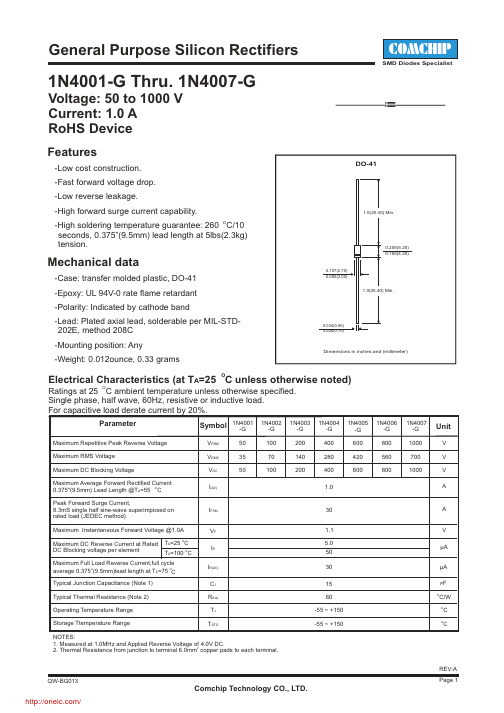
OElectrical Characteristics (at T A =25 C unless otherwise noted)ORatings at 25 C ambient temperature unless otherwise specified.Single phase, half wave, 60Hz, resistive or inductive load.For capacitive load derate current by 20%.ParameterSymbol UnitMaximum Repetitive Peak Reverse Voltage Maximum RMS Voltage Maximum DC Blocking VoltageMaximum Average Forward Rectified Current O 0.375"(9.5mm) Lead Length @T A =55C Peak Forward Surge Current, 8.3mS single half sine-wave superimposed on rated load (JEDEC method)Maximum Instantaneous Forward Voltage @1.0A Maximum DC Reverse Current at RatedOperating Temperature Range Storage Ttemperature RangeO T A =25C DC Blocking voltage per element Typical Junction Capacitance (Note 1)Typical Thermal Resistance (Note 2)503550V RRM V RMS V DC I (AV)I FSM V F I R C J R θJA T J T STG1.0305.0501560-55 ~ +150-55 ~ +150V V V AA V P FOC OCμA OC/WNOTES:1. Measured at 1.0MHz and Applied Reverse Voltage of 4.0V DC.22. Thermal Resistance from junction to terminal 6.0mm copper pads to each terminal.Voltage: 50 to 1000 V Current: 1.0 A RoHS DeviceFeatures-Low cost construction. -Fast forward voltage drop. -Low reverse leakage.-High forward surge current capability.O -High soldering temperature guarantee: 260C/10 seconds, 0.375”(9.5mm) lead length at 5lbs(2.3kg) tension.Mechanical data-Case: transfer molded plastic, DO-41 -Epoxy: UL 94V-0 rate flame retardant -Polarity: Indicated by cathode band-Lead: Plated axial lead, solderable per MIL-STD-202E, method 208C -Mounting position: Any-Weight: 0.012ounce, 0.33 grams10070100200140200400280400600420600800560800100070010001N4001-G Thru. 1N4007-G1.130-G 4001 1N -G 4002 1N -G 4003 1N -G 4004 1N -G 40051N -G 4006 1N -G 4007 1N O T A =100C Maximum Full Load Reverse Current,full cycle average 0.375”(9.5mm)lead length at T L =75 C O I R(AV)μARating and Characteristic Curves ( 1N4001) -G Thru. 4007-G1N Fig.2 Maximum. Non-Repetitive PeakForward Surge Current0ΙF S M , P e a k F o r w a r d S u r g e C u r r e n t (A )Number of Cycles at 60Hz1Fig.1 Typical Forward CurrentDerating CurveI (A V ), A v e r a g e F o r w a r d C u r r e n t (A )OT A , Ambient Temperature (C)02575175Fig.3 Typical Instantaneous ForwardCharacteristics0.01I F , I n s t a n t a n e o u s F o r w a r d C u r r e n t (A )V F , Instantaneous Forward Voltage (V)1.00.61.01.400.61.01.62.010015351.20.1Fig.4 Typical Reverse Characteristics0.01I R , I n s t a n t a n e o u s R e v e r s e C u r r e n t (m A )Percent of Peak Reverse Voltage (%)1.0100.11001250.40.80.81.8Fig.5 Typical Junction Capacitance10C J , C a p a c i t a n c e (p F )V R , Reverse Voltage (V)1000.11010010501500.21051025301.24080100140201206012010205025分销商库存信息: COMCHIP1N4002-G。
IXGP7N60C;IXGA7N60C;中文规格书,Datasheet资料

© 2002 IXYS All rights reserved98564A (06/02)Symbol Test Conditions Maximum RatingsVCES TJ= 25°C to 150°C600VVCGR TJ= 25°C to 150°C; RGE= 1 MΩ600VVGESContinuous±20VVGEMTransient±30VI C25TC= 25°C 14AI C90TC= 90°C 7AI CM TC= 25°C, 1 ms 30ASSOA VGE = 15 V, TVJ= 125°C, RG= 22 Ω ICM= 14A(RBSOA)Clamped inductive load, L = 300 µH @ 0.8 VCESPC TC= 25°C 54WTJ-55 (150)TJM150CTstg-55 (150)Maximum lead temperature for soldering 300C 1.6 mm (0.062 in.) from case for 10 sMd Mounting torque, (TO-220) M3 0.45/4 Nm/lb.in.M3.5 0.55/5 Nm/lb.in.Weight TO-220 4g TO-263 2 g Symbol Test Conditions Characteristic Values(TJ = 25°C, unless otherwise specified)min.typ.max.BVCESIC= 250 µA, VGE= 0 V600VVGE(th)IC= 250 µA, VCE= VGE2.5 5.5VI CES VCE= 0.8 • VCESTJ= 25°C100µA VGE= 0 V TJ= 125°C500µAI GES VCE= 0 V, VGE= ±20 V±100nAVCE(sat)IC= IC90, VGE= 15 V 2.0 2.7VFeatures•International standard packagesJEDEC TO-263 surfacemountable and JEDEC TO-220 AB•High frequency IGBT•High current handling capability•HiPerFAST TM HDMOS TM process•MOS Gate turn-on-drive simplicityApplications•Uninterruptible power supplies (UPS)•Switched-mode and resonant-modepower supplies•AC motor speed control•DC servo and robot drives•DC choppersAdvantages•High power density•Suitable for surface mounting•Very low switching losses for highfrequency applicationsVCES=600VIC25=14AVCE(sat)= 2.7Vtfi=45nsG = Gate, C = Collector,E = Emitter,TAB = CollectorHiPerFAST TM IGBT Lightspeed TM Series IXGA 7N60CIXGP 7N60CGEC (TAB)TO-263 AA (IXGA)TO-220AB (IXGP)IXYS reserves the right to change limits, test conditions, and dimensions.IXYS MOSFETs and IGBTs are covered by one or more of the following U.S. patents:4,835,5924,881,1065,017,5085,049,9615,187,1175,486,7156,306,728B14,850,0724,931,8445,034,7965,063,3075,237,4815,381,025SymbolTest ConditionsCharacteristic ValuesTO-220 AB Outlinelimeter Inches Min.Max.Min.Max.A 12.7013.970.5000.550B 14.7316.000.5800.630C9.9110.660.3900.420D 3.54 4.080.1390.161E 5.85 6.850.2300.270F 2.54 3.180.1000.125G 1.15 1.650.0450.065H 2.79 5.840.1100.230J 0.64 1.010.0250.040K 2.54BSC 0.100BSC M 4.32 4.820.1700.190N 1.14 1.390.0450.055Q 0.350.560.0140.022R2.29 2.790.0900.110TO-263 AA OutlinePins:1 - Gate2 - Collector3 - Emitter4 - CollectorBottom SideMin. Recommended Footprint (Dimensions in inches and mm)分销商库存信息:IXYSIXGP7N60C IXGA7N60C。
IXGR12N60C;中文规格书,Datasheet资料
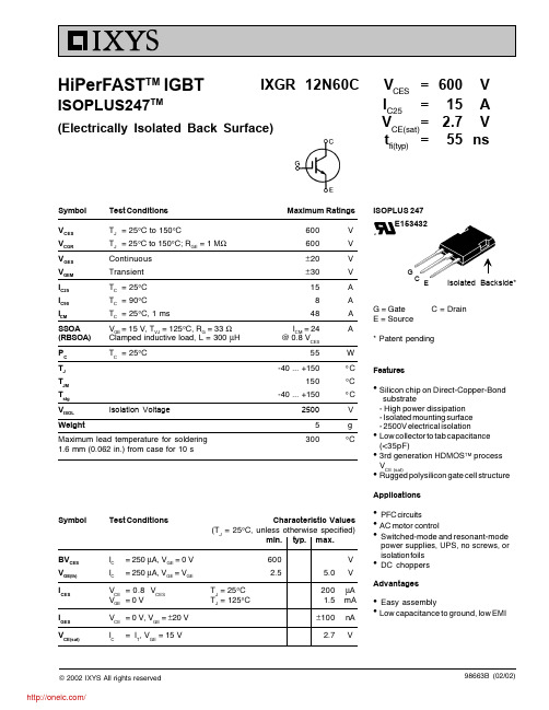
© 2002 IXYS All rights reservedSymbol Test Conditions Maximum RatingsV CES T J = 25°C to 150°C600V V CGR T J = 25°C to 150°C; R GE = 1 M Ω600V V GES Continuous ±20V V GEM Transient ±30V I C25T C = 25°C 15A I C90T C = 90°C 8A I CMT C = 25°C, 1 ms48A SSOAV GE = 15 V, T VJ = 125°C, R G = 33 Ω I CM = 24A(RBSOA)Clamped inductive load, L = 300 µH @ 0.8 V CESP C T C = 25°C55W T J -40 ... +150°C T JM 150°CT stg -40 ... +150°C V ISOL Isolation Voltage 2500V Weight5g Maximum lead temperature for soldering 300°C1.6 mm (0.062 in.) from case for 10 s98663B (02/02)Symbol Test ConditionsCharacteristic Values(T J = 25°C, unless otherwise specified)min.typ.max.BV CES I C = 250 µA, V GE = 0 V 600V V GE(th)I C= 250 µA, V GE = V GE2.55.0V I CES V CE = 0.8 V CES T J = 25°C 200µA V GE = 0 VT J = 125°C1.5mA I GES V CE = 0 V, V GE =±20 V ±100nA V CE(sat)I C= I T , V GE = 15 V2.7VV CES =600 VI C25=15A V CE(sat)= 2.7 Vt fi(typ)=55ns HiPerFAST TM IGBTISOPLUS247TM(Electrically Isolated Back Surface)G = Gate C = DrainE = Source* Patent pendingFeatureslSilicon chip on Direct-Copper-Bond substrate- High power dissipation - Isolated mounting surface - 2500V electrical isolationlLow collector to tab capacitance (<35pF)l 3rd generation HDMOS TM process V CE (sat)lRugged polysilicon gate cell structureApplicationslPFC circuitsl AC motor controllSwitched-mode and resonant-mode power supplies, UPS, no screws, or isolation foils lDC choppersAdvantagesl Easy assemblylLow capacitance to ground, low EMIIXGR 12N60CISOPLUS 247E153432Isolated Backside*IXYS reserves the right to change limits, test conditions, and dimensions.IXYS MOSFETS and IGBTs are covered by one or more of the following U.S. patents:4,835,5924,881,1065,017,5085,049,9615,187,1175,486,7156,306,728B14,850,0724,931,8445,034,7965,063,3075,237,4815,381,025SymbolTest ConditionsCharacteristic Values(T= 25°C, unless otherwise specified)Note: I T = 12A分销商库存信息: IXYSIXGR12N60C。
12N60中文资料
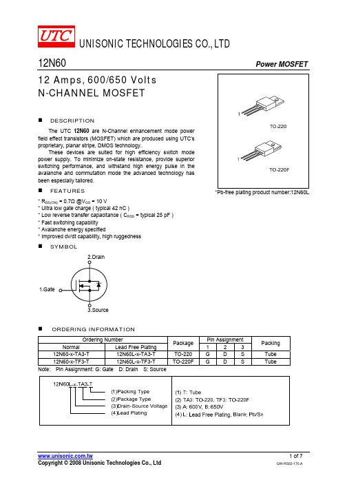
Fig. 3A Gate Charge Test Circuit
Fig. 3B Gate Charge Waveform
10V
RD tp
L VDS
BVDSS IAS
VDD
VDD D.U.T.
ID(t) tp
VDS(t) Time
Fig. 4A Unclamped Inductive Switching Test Circuit Fig. 4B Unclamped Inductive Switching Waveforms
25℃ 100
55℃
10-1 2
Notes:
1.VDS=50V 2.250μs Pulse Test
4
6
8
10
Gate-Source Voltage, VGS (V)
UNISONIC TECHNOLOGIES CO., LTD
12N60-x-TF3-T
12N60L-x-TF3-T
Note: Pin Assignment: G: Gate D: Drain S: Source
Package
TO-220 TO-220F
Pin Assignment
1
2
3
G
D
S
G
D
S
Packing
Tube Tube
Copyright © 2008 Unisonic Technologies Co., Ltd
Turn-On Rise Time Turn-Off Delay Time
tR tD(OFF)
VDD = 300V, ID = 12A, RG = 25Ω (Note 4, 5)
115 240 nsቤተ መጻሕፍቲ ባይዱ95 200 ns
IXGH48N60C3D1;中文规格书,Datasheet资料

Coes 100
Cres
20 10
10 0 5 10 15 20 25 30 35 40
0 200
250
300
350
400
450
500
550
600
650
VCE - Volts
VCE - Volts
Fig. 11. Maximum Transient Thermal Impedance
1.00
Z(th)JC - ºC / W
Inches Min. Max. .185 .209 .087 .102 .059 .098 .040 .055 .065 .084 .113 .123 .016 .031 .819 .845 .610 .640 0.205 0.225 .780 .800 .177 .140 .144 0.232 0.252 .170 .216
VCE(sat) - Normalized
IC - Amperes
40 35 30 25 20 15 10 5 0 0 0.4 0.8 1.2 1.6 2 2.4 2.8 7V 9V
1.0 0.9 0.8 0.7 0.6 0.5 25 50 75 I
C
C
= 30A
I
C
= 15A
100
125
150
VCE - Volts
Characteristic Values Min. Typ. Max. 3.0 5.5 V 300 μA 1.75 mA ±100 2.3 1.8 2.5 nA V V
z z z z z z z
High Frequency Power Inverters UPS Motor Drives SMPS PFC Circuits Battery Chargers Welding Machines Lamp Ballasts
IXGH30N60中文资料
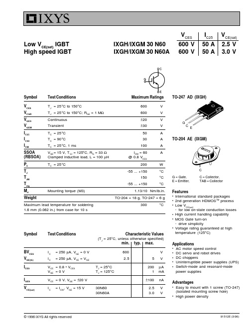
© 1996 IXYS All rights reservedTO-247 AD (IXGH)V CESI C25V CE(sat)Low V CE(sat) IGBT IXGH/IXGM 30 N60600 V 50 A 2.5 V High speed IGBTIXGH/IXGM 30 N60A600 V50 A3.0 VGCESymbol Test Conditions Maximum RatingsV CES T J = 25°C to 150°C600V V CGR T J = 25°C to 150°C; R GE = 1 M Ω600V V GES Continuous ±20V V GEM Transient ±30V I C25T C = 25°C 50A I C90T C = 90°C 30A I CMT C = 25°C, 1 ms100A SSOA V GE = 15 V, T VJ = 125°C, R G = 33 Ω I CM = 60A (RBSOA)Clamped inductive load, L = 100 µH @ 0.8 V CESP C T C = 25°C200W T J -55 ... +150°C T JM 150°C T stg -55 ... +150°CM d Mounting torque (M3) 1.13/10Nm/lb.in.WeightTO-204 = 18 g, TO-247 = 6gMaximum lead temperature for soldering 300°C1.6 mm (0.062 in.) from case for 10 sSymbol Test ConditionsCharacteristic Values(T J= 25°C, unless otherwise specified)min.typ.max.BV CES I C = 250 µA, V GE = 0 V 600V V GE(th)I C= 250 µA, V CE = V GE2.55V I CES V CE = 0.8 • V CES T J = 25°C 200µA V GE = 0 VT J= 125°C1mA I GES V CE = 0 V, V GE = ±20 V ±100nA V CE(sat)I C= I C90, V GE = 15 V30N60 2.5V 30N60A3.0VTO-204 AE (IXGM)CG = Gate, C = Collector,E = Emitter,TAB = CollectorFeaturesl International standard packages l 2nd generation HDMOS TM process l Low V CE(sat)-for low on-state conduction losses l High current handling capability l MOS Gate turn-on -drive simplicitylVoltage rating guaranteed at high temperature (125°C)Applicationsl AC motor speed control l DC servo and robot drives l DC choppersl Uninterruptible power supplies (UPS)lSwitch-mode and resonant-mode power suppliesAdvantageslEasy to mount with 1 screw (TO-247)(isolated mounting screw hole)lHigh power density91512E (3/96)IXYS MOSFETS and IGBTs are covered by one or more of the following U.S. patents:4,835,5924,881,1065,017,5085,049,9615,187,1175,486,7154,850,0724,931,8445,034,7965,063,3075,237,4815,381,025IXYS reserves the right to change limits, test conditions, and dimensions.SymbolTest ConditionsCharacteristic Values(T J = 25°C, unless otherwise specified)min.typ.max.g fs I C = I C90; V CE = 10 V,816S Pulse test, t ≤ 300 µs, duty cycle ≤ 2 %C ies 2800pF C oes V CE = 25 V, V GE = 0 V, f = 1 MHz230pF C res 70pF Q g 150180nC Q ge I C = I C90, V GE = 15 V, V CE = 0.5 V CES 3550nC Q gc 6090nC t d(on)100ns t ri 200ns t d(off)500ns t fi 30N60A 200ns E off 30N60A 2mJ t d(on)100ns t ri 200ns E on 3mJ t d(off)6001000ns t fi 30N605001500ns 30N60A250800ns E off 30N605.5mJ 30N60A 4.0mJ R thJC 0.62K/WR thCK0.25K/WIXGH 30N60 and IXGH 30N60A characteristic curves are located on theIXGH 30N60U1 and IXGH 30N60AU1 data sheets.Inductive load, T J = 25°CI C = I C90, V GE = 15 V, L = 300 µH V CE = 0.8 V CES , R G = R off = 33 ΩSwitching times may increasefor V CE (Clamp) > 0.8 • V CES ,higher T J or increased R GInductive load, T J = 125°C I C = I C90, V GE = 15 V,L = 300 µH V CE = 0.8 V CES ,R G = R off = 33 ΩRemarks: Switching timesmay increase for V CE(Clamp) > 0.8 • V CES , higher T J or increased R G。
STGP12NB60HD;中文规格书,Datasheet资料

1/9October 2003STGP12NB60HDN-CHANNEL 18A -600V TO-220PowerMESH™IGBTs HIGH INPUT IMPEDANCEs LOW ON-VOLTAGE DROP (V cesat )s OFF LOSSES INCLUDE TAIL CURRENT s LOW GATE CHARGEs HIGH CURRENT CAPABILITYs VERY HIGH FREQUENCY OPERATION sCO-PACKAGED WITH TURBOSWITCHT ANTIPARALLEL DIODEDESCRIPTIONUsing the latest high voltage technology based on a patented strip layout,STMicroelectronics has de-signed an advanced family ofIGBTs,the Power-MESH™IGBTs,with outstanding perfomances.The suffix "H"identifies a family optimized for high frequency applications (up to 50kHz)in order to achieve very high switching performances (reduced tfall)mantaining a lowvoltage drop.APPLICATIONSs HIGH FREQUENCY MOTOR CONTROLSs SMPS and PFC IN BOTH HARD SWITCH AND RESONANT TOPOLOGIES s UPSORDERING INFORMATIONTYPE V CES V CE(sat)(Max)@25°CI C@100°CSTGP12NB60HD600V<2.8 V 18ASALES TYPE MARKING PACKAGE PACKAGINGSTGP12NB60HDGP12NB60HDTO-220TUBEl s Ob so e t ePr od u c t () -l s l u )Ob so e t ePr od u c t () -O bs o e t eP r od c t(sSTGP12NB60HD2/9ABSOLUTE MAXIMUM RATINGS( )Pulse width limited by safe operating areaTHERMAL DATAELECTRICAL CHARACTERISTICS (T CASE =25°C UNLESS OTHERWISE SPECIFIED)OFFON (1)DYNAMICSymbol ParameterValue Unit V CES Collector-Emitter Voltage (V GS =0)600V V ECR Emitter-Collector Voltage 20V V GE Gate-Emitter Voltage±20V I C Collector Current (continuous)at T C =25°C (#)30A I C Collector Current (continuous)at T C =100°C (#)18A I CM ( )Collector Current (pulsed)60A P TOT Total Dissipation at T C =25°C 125W Derating Factor 1.0W/°C T stg Storage Temperature–65to 150°C T jMax.Operating Junction Temperature150°CRthj-case Thermal Resistance Junction-case Max 1.0°C/W Rthj-ambThermal Resistance Junction-ambient Max62.5°C/WSymbol ParameterTest ConditionsMin.Typ.Max.Unit V BR(CES)Collector-Emitter Breakdown Voltage I C =250µA,V GE =0600V I CES Collector cut-off (V GE =0)V CE =Max Rating,T C =25°C 50µA V CE =Max Rating,T C =125°C100µA I GESGate-Emitter Leakage Current (V CE =0)V GE =±20V ,V CE =0±100nASymbol ParameterTest ConditionsMin.Typ.Max.Unit V GE(th)Gate Threshold VoltageV CE =V GE ,I C =250µA 35V V CE(sat)Collector-Emitter Saturation VoltageV GE =15V,I C =12A2.0 2.8V V GE =15V,I C =12A,Tj =125°C1.7VSymbol Parameter Test ConditionsMin.Typ.Max.Unit g fsForward Transconductance V CE =15V ,I C =12A10S C iesInput Capacitance V CE =25V,f =1MHz,V GE =0920pF C oes Output Capacitance 120pF C res Reverse Transfer Capacitance27pF Q g Q ge Q gc Total Gate Charge Gate-Emitter Charge Gate-Collector Charge V CE =480V,I C =12A,V GE =15V681030nCnC nC I CLLatching CurrentV clamp =480V , Tj =150°C R G =10Ω48Al t l c )Ob so e t ePr od u c (s ) -O bs o e t eP r od u t (s3/9STGP12NB60HDELECTRICAL CHARACTERISTICS (CONTINUED)SWITCHING ONSWITCHING OFFCOLLECTOR-EMITTER DIODENote: 1.Pulsed:Pulse duration =300µs,duty cycle 1.5%.2.Pulse width limited by max.junction temperature.(**)Losses include Also the Tail (Jedec Standardization)(#)Calculated according to the iterative formula:Symbol ParameterTest ConditionsMin.Typ.Max.Unit t d(on)t r Turn-on Delay Time Rise TimeV CC =480V,I C =12A R G =10Ω,V GE =15V 546ns ns (di/dt)on EonTurn-on Current Slope Turn-on Switching LossesV CC =480V,I C =12A R G =10Ω,V GE =15V,Tj =125°C700290A/µs µJSymbol ParameterTest ConditionsMin.Typ.Max.Unit t c Cross-over Time V cc =480V,I C =12A,R GE =10Ω,V GE =15V150ns t r (V off )Off Voltage Rise Time 27ns t d (off )Delay Time 91ns t f Fall Time100nsE off (**)Turn-off Switching Loss 0.21m J E ts Total Switching Loss 0.49m Jt c Cross-over Time V cc =480V,I C =12A,R GE =10Ω,V GE =15V Tj =125°C230ns t r (V off )Off Voltage Rise Time 76ns t d (off )Delay Time 95ns t f Fall Time200nsE off (**)Turn-off Switching Loss 0.45m J E tsTotal Switching Loss0.74m JSymbolParameterTest ConditionsMin.Typ.Max.Unit I f I fm Forward CurrentForward Current pulsed 1248A A V f Forward On-VoltageI f =6AI f =6A,Tj =125°C1.31.1 1.9V V t rr Q rr I rrmReverse Recovery Time Reverse Recovery Charge Reverse Recovery CurrentI f =6A ,V R =50V,Tj =125°C,di/dt =100A/µs802405.5ns nC AI C T C ()T JMAX T C–R THJ C –V CESAT MAX ()T C I C ,()×--------------------------------------------------------------------------------------=-O STGP12NB60HDO-O 5/9STGP12NB60HDNormalized Breakdown Voltage vs TemperatureTotal Switching Losses vs TemperatureGate Charge vs Gate-Emitter Voltage Total Switching Losses vs Collector Currentll c Ob so e t eP-O bs o e t eP r od u t (STGP12NB60HD6/9l)O b s oe t eP ro d7/9STGP12NB60HDFig.2:Test Circuit For Inductive Load SwitchingFig.1:Gate Charge test CircuitSTGP12NB60HD8/9l slc)O b s oe t eP ro du ct()-O bs oe t eP ro dut(s9/9STGP12NB60HDInformation furnished is believed to be accurate and reliable. However, STMicroelectronics assumes no responsibility for the consequences of use of such information nor for any infringement of patents or other rights of third parties which may result from its use. No license is granted by implication or otherwise under any patent or patent rights of STMicroelectronics. Specifications mentioned in this publication are subject to change without notice. This publication supersedes and replaces all information previously supplied. STMicroelectronics products are not authorized for use as critical components in life support devices or systems without express written approval of STMicroelectronics.© The ST logo is a registered trademark of STMicroelectronics© 2003 STMicroelectronics - Printed in Italy - All Rights ReservedSTMicroelectronics GROUP OF COMPANIESAustralia - Brazil - Canada - China - Finland - France - Germany - Hong Kong - India - Israel - Italy - Japan - Malaysia - Malta - MoroccoSingapore - Spain - Sweden - Switzerland - United Kingdom - United States.© 分销商库存信息: STMSTGP12NB60HD。
HGTP12N60A4D_NL中文资料

HGTG12N60A4D, HGTP12N60A4D, HGT1S12N60A4DS
Data Sheet December 2001
600V, SMPS Series N-Channel IGBT with Anti-Parallel Hyperfast Diode
The HGTG12N60A4D, HGTP12N60A4D and HGT1S12N60A4DS are MOS gated high voltage switching devices combining the best features of MOSFETs and bipolar transistors. These devices have the high input impedance of a MOSFET and the low on-state conduction loss of a bipolar transistor. The much lower on-state voltage drop varies only moderately between 25 oC and 150oC. The IGBT used is the development type TA49335. The diode used in anti-parallel is the development type TA49371. This IGBT is ideal for many high voltage switching applications operating at high frequencies where low conduction losses are essential. This device has been optimized for high frequency switch mode power supplies. Formerly Developmental Type TA49337.
常用三极管参数excel

玉林万顺达电脑芯片级维修资料 2010-07-20整理玉林万顺达电脑芯片级维修资料 2010-07-20整理玉林万顺达电脑芯片级维修资料 2010-07-20整理玉林万顺达电脑芯片级维修资料 2010-07-20整理玉林万顺达电脑芯片级维修资料 2010-07-20整理玉林万顺达电脑芯片级维修资料 2010-07-20整理玉林万顺达电脑芯片级维修资料 2010-07-20整理玉林万顺达电脑芯片级维修资料 2010-07-20整理玉林万顺达电脑芯片级维修资料 2010-07-20整理玉林万顺达电脑芯片级维修资料 2010-07-20整理玉林万顺达电脑芯片级维修资料 2010-07-20整理玉林万顺达电脑芯片级维修资料 2010-07-20整理玉林万顺达电脑芯片级维修资料 2010-07-20整理玉林万顺达电脑芯片级维修资料 2010-07-20整理玉林万顺达电脑芯片级维修资料 2010-07-20整理玉林万顺达电脑芯片级维修资料 2010-07-20整理玉林万顺达电脑芯片级维修资料 2010-07-20整理玉林万顺达电脑芯片级维修资料 2010-07-20整理玉林万顺达电脑芯片级维修资料 2010-07-20整理玉林万顺达电脑芯片级维修资料 2010-07-20整理玉林万顺达电脑芯片级维修资料 2010-07-20整理玉林万顺达电脑芯片级维修资料 2010-07-20整理玉林万顺达电脑芯片级维修资料 2010-07-20整理玉林万顺达电脑芯片级维修资料 2010-07-20整理玉林万顺达电脑芯片级维修资料 2010-07-20整理玉林万顺达电脑芯片级维修资料 2010-07-20整理玉林万顺达电脑芯片级维修资料 2010-07-20整理玉林万顺达电脑芯片级维修资料 2010-07-20整理玉林万顺达电脑芯片级维修资料 2010-07-20整理玉林万顺达电脑芯片级维修资料 2010-07-20整理。
- 1、下载文档前请自行甄别文档内容的完整性,平台不提供额外的编辑、内容补充、找答案等附加服务。
- 2、"仅部分预览"的文档,不可在线预览部分如存在完整性等问题,可反馈申请退款(可完整预览的文档不适用该条件!)。
- 3、如文档侵犯您的权益,请联系客服反馈,我们会尽快为您处理(人工客服工作时间:9:00-18:30)。
/
分销商库存信息:
IXYS IXGH12N60CD1
l
Very high frequency IGBT New generation HDMOSTM process International standard package JEDEC TO-247AD High peak current handling capability
Symbol
Test Conditions
Inches Min. Max. .185 .209 .087 .102 .059 .098 .040 .055 .065 .084 .113 .123 .016 .031 .819 .845 .610 .640 0.205 0.225 .780 .800 .177 .140 .144 0.232 0.252 .170 .216 242 BSC
1.25 K/W K/W
Reverse Diode (FRED) Symbol VF Test Conditions I F = 15A; T VJ = 150 ° C T VJ = 25 ° C
Characteristic Values (TJ = 25°C, unless otherwise specified) min. typ. max. 1.7 2.5 2 2.5 V V A
C = Collector, TAB = Collector
Mounting torque with screw M3 Mounting torque with screw M3.5
0.45/4 Nm/lb.in. 0.55/5 Nm/lb.in. 6 300 g °C Features
l l l
Maximum lead temperature for soldering 1.6 mm (0.062 in.) from case for 10 s
l
PFC circuit AC motor speed control DC servo and robot drives Switch-mode and resonant-mode power supplies High power audio amplifiers
Advantages
Hale Waihona Puke l lFast switching speed High power density
Maximum Ratings 600 600 ± 20 ± 30 24 12 48 ICM = 24 @ 0.8 VCES 100 -55 ... +150 150 -55 ... +150 V V V V A A A A W °C °C °C
TO-247 AD
C (TAB) G C E
G = Gate, E = Emitter,
∅P
TO-247 AD Outline
gfs Cies Coes Cres Qg Qge Qgc td(on) tri td(off) tfi Eoff td(on) tri Eon td(off) tfi Eoff RthJC RthCK
IC = IC90; VCE = 10 V, Pulse test, t ≤ 300 µs, duty cycle ≤ 2 %
Characteristic Values (TJ = 25°C, unless otherwise specified) min. typ. max. 600 2.5 TJ = 25°C TJ = 125°C 5.0 200 1.5 ± 100 2.1 2.7 V V µA mA nA V
Applications
© 2002 IXYS All rights reserved
98623A (2/02)
/
IXGH 12N60CD1
Symbol Test Conditions Characteristic Values (TJ = 25°C, unless otherwise specified) min. typ. max. 5 11 860 VCE = 25 V, VGE = 0 V, f = 1 MHz 100 15 32 IC = IC90, VGE = 15 V, VCE = 0.5 VCES Inductive load, TJ = 25°C IC = IC90, VGE = 15 V, L = 300 µH VCE = 0.8 VCES, RG = Roff = 18 Ω Remarks: Switching times may increase for VCE (Clamp) > 0.8 VCES, higher TJ or increased RG Inductive load, TJ = 125°C IC = IC90, VGE = 15 V, L = 300 µH VCE = 0.8 VCES, RG = Roff = 18 Ω Remarks: Switching times may increase for VCE (Clamp) > 0.8 VCES, higher TJ or increased RG IGBT 0.25 10 10 20 20 60 55 0.09 20 20 0.5 85 85 0.27 180 180 0.60 S
HiPerFASTTM IGBT LightspeedTM Series
IXGH 12N60CD1
VCES = 600 V IC25 = 24 A VCE(sat) = 2.7 V tfi(typ) = 55 ns
Symbol VCES VCGR VGES VGEM IC25 IC90 ICM SSOA (RBSOA) PC TJ TJM Tstg Md Weight
l l
BVCES VGE(th) ICES IGES VCE(sat)
IC IC
= 250 µA, VGE = 0 V = 250 µA, VGE = VGE
l l
VCE = 0.8 VCES VGE = 0 V VCE = 0 V, VGE = ±20 V IC = ICE90, VGE = 15 V
IRM t rr RthJC
V R = 100 V; I F =25A; -di F /dt = 100 A/ µ s L < 0.05 µ H ; T VJ = 100 ° C IF = 1 A; -di/dt = 50 A/µs; VR = 30 V TJ = 25°C Diode
35
ns 1.6 K/W
Test Conditions TJ = 25°C to 150°C TJ = 25°C to 150°C; RGE = 1 MΩ Continuous Transient TC = 25°C TC = 90°C TC = 25°C, 1 ms VGE = 15 V, TVJ = 125°C, RG = 33 Ω Clamped inductive load, L = 300 µH TC = 25°C
pF pF pF nC nC nC ns ns ns ns mJ ns ns mJ ns ns mJ
e
Dim.
Millimeter Min. Max. A 4.7 5.3 A1 2.2 2.54 2.2 2.6 A2 b 1.0 1.4 b1 1.65 2.13 b2 2.87 3.12 C .4 .8 D 20.80 21.46 E 15.75 16.26 e 5.20 5.72 L 19.81 20.32 L1 4.50 ∅P 3.55 3.65 Q 5.89 6.40 R 4.32 5.49 S 6.15 BSC
IXYS reserves the right to change limits, test conditions, and dimensions.
IXYS MOSFETS and IGBTs are covered by one or more of the following U.S. patents: 4,835,592 4,850,072 4,881,106 4,931,844 5,017,508 5,034,796 5,049,961 5,063,307 5,187,117 5,237,481 5,486,715 5,381,025 6,306,728B1