HT7033A中文资料
HT7333文档

高耐压低压差微功耗型HT73## 系列CMOS 电压稳压电路 250mAHT73##系列是使用CMOS技术开发的低压差,高精度输出电压,超低功耗电流的正电压型电压稳压电路。
由于置有低通态电阻晶体管,因而输入输出压差低。
同时具有高输入电压承受能力,最高工作电压可达12V,适合需要较高耐压的应用电路。
■特性:·输出电压精度高。
精度±3%·输入输出压差低。
典型值5mV·超低功耗电流。
典型值⒈2uA·低输出电压温漂典型值50 PPm /℃·高输入耐压。
升至12V保持输出稳压·输出短路保护短路电流小于100 mA■用途:·使用电池供电设备的稳压电源·通信设备的稳压电源·家电玩具的稳压电源·移动用的稳压电源·便携式医用仪器稳压电源■产品目录型号输出电压〔注〕误差HT7330 3.0V ±3%HT7333 3.3V ±3%HT7336 3.6V ±3%HT7344 4.4V ±3%HT7350 5.0V ±3% 注: 在希望使用上述输出电压档以外的产品,客户可要求定制,输出电压围1.5V~12V,每0.1V 进展细分。
■封装:■绝对最大额定值:〔除特殊注明以外:Ta=25℃〕注意绝对最大额定值是指无论在任何条件下都不能超过的额定值。
万一超过此额定值,有可能造成产品劣化等物理性损伤。
■电气属性:HT73##系列〔HT7330,输出电压+3.0V〕〔除特殊注明以外:Ta=25℃〕*⒈缓慢增加输出电流,当输出电压为小于V OUT的98%时的输出电流值*⒉V drop=V IN1-〔V OUT〔E〕×0.98V〕V OUT〔E〕:V IN=V OUT+2V,I OUT=1 mA时的输出电压值V IN1:缓慢下降输出电压,当输出电压降为V OUT〔E〕的98%时的输入电压测定电路1.2.3.标准电路:注意上述连接图以与参数并不作为保证电路工作的依据。
HT7022A中文资料

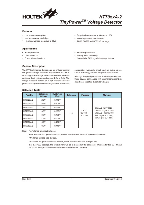
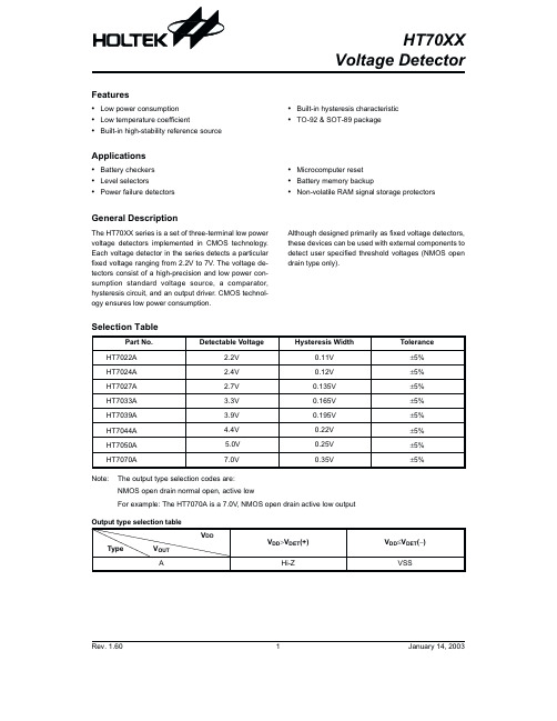
HT70XXVoltage DetectorSelection TablePart No.Detectable VoltageHysteresis WidthTolerance HT7022A 2.2V 0.11V ±5%HT7024A 2.4V 0.12V ±5%HT7027A 2.7V 0.135V ±5%HT7033A 3.3V 0.165V ±5%HT7039A 3.9V 0.195V ±5%HT7044A 4.4V 0.22V ±5%HT7050A 5.0V 0.25V ±5%HT7070A 7.0V0.35V±5%Note:The output type selection codes are:NMOS open drain normal open,active lowFor example:The HT7070A is a 7.0V,NMOS open drain active low outputOutput type selection tableV DDV DD >V DET (+)V DD £V DET (-)TypeV OUT AHi-ZVSSRev.1.601January 14,2003General DescriptionThe HT70XX series is a set of three-terminal low power voltage detectors implemented in CMOS technology.Each voltage detector in the series detects a particular fixed voltage ranging from 2.2V to 7V.The voltage de-tectors consist of a high-precision and low power con-sumption standard voltage source,a comparator,hysteresis circuit,and an output driver.CMOS technol-ogy ensures low power consumption.Although designed primarily as fixed voltage detectors,these devices can be used with external components to detect user specified threshold voltages (NMOS open drain type only).Features·Low power consumption ·Low temperature coefficient·Built-in high-stability reference source·Built-in hysteresis characteristic ·TO-92&SOT-89packageApplications·Battery checkers ·Level selectors ·Power failure detectors·Microcomputer reset ·Battery memory backup·Non-volatile RAM signal storage protectorsBlock DiagramN channel open drain output(normal open;active low)A typePin AssignmentRev.1.602January14,2003Pad AssignmentHT70XX (except HT7022A)Chip size:1317´1158(m m)2*The IC substrate should be connected to VDD in the PCB layout artwork.HT7022A onlyChip size:2032´1321(m m)2*The IC substrate should be connected to VDD in the PCB layout artwork.Absolute Maximum RatingsSupply Voltage,except HT7022A..................................................................................................V SS -0.3V to V SS +26V Supply Voltage,HT7022A only....................................................................................................................-0.3V to13V Output Voltage...........................V SS -0.3V to V DD +0.3V Output Current......................................................50mA Storage Temperature............................-50°C to 125°C Power Consumption..........................................200mWOperating Temperature 0°C to 70°CNote:These are stress ratings only.Stresses exceeding the range specified under ²Absolute Maximum Ratings ²maycause substantial damage to the device.Functional operation of this device at other conditions beyond those listed in the specification is not implied and prolonged exposure to extreme conditions may affect device reliabil-ity.Rev.1.603January 14,2003Pad CoordinatesHT70XX (except HT7022A)Unit:m m Pad No.X Y 1-483.30-379.502-234.60-399.503443.90-386.00HT7022A onlyUnit:m mPad No.X Y1-434.34394.972120.65461.013774.70412.75Electrical CharacteristicsHT7022A Ta=25°CHT7024A Ta=25°CHT7027A Ta=25°CRev.1.604January14,2003HT7039A Ta=25°CHT7044A Ta=25°CRev.1.605January14,2003HT7070A Ta=25°CRev.1.606January 14,2003Functional DescriptionThe HT70XX series is a set of voltage detectors equipped with a high stability voltage reference which is connected to the negative input of a comparator ¾de-noted as V REF in the following figure for NMOS output voltage detector.When the voltage drop to the positive input of the com-parator (i,e,V B )is higher than V REF ,VOUT goes high,M1turns off,and V B is expressed as V BH =V DD ´(R B +R C )/(R A +R B +R C ).If V DD is decreased so that V B falls to a value less than V REF ,the comparator output in-verts from high to low,V OUT goes low,V C is high,M1turns on,RC is bypassed,and V B becomes:V BL =V DD ´R B /(R A +R B ),which is less than V BH.By so doing,the comparator output will stay low to prevent the circuit from oscillating when V B »V REF.If V DD falls below the minimum operating voltage,the output becomes undefined.When VDD goes from low to V DD ´R B /(R A +R B )>V REF ,the comparator output and V OUT goes high.The detectable voltage is defined as:V DET (-)=R R R R R A B CB C +++´V REFThe release voltage is defined as:V DET (+)=R R R A BB+´V REFThe hysteresis width is:V HYS=V DET(+)-V DET(-)The figure demonstrates the NMOS output type withpositive output polarity(V OUT is normally open,activelow).The HT70XX series also supplies options for otheroutput types with active high outputs.Application cir-cuits shown are examples of positive output polarity(normally open,active low)unless otherwise specified.NMOS output voltage detector(HT70XXA) Application CircuitsMicrocomputer reset circuitNormally a reset circuit is required to protect the micro-computer system from malfunctions due to power line interruptions.The following examples show how differ-ent output configurations perform a reset function in var-ious systems.·NMOS open drain output application for separate power supply·NMOS open drain output application with R-C delayPower-on reset circuitWith several external components,the NMOS open drain type of the HT70XX series can be used to perform a power-on reset function as shown:Rev.1.607January14,20035V power line monitoring circuitGenerally,a minimum operating voltage of4.5V is guar-anteed in a5V power line system.The HT7044A is rec-ommended for use as5V power line monitoring circuit.·5V power line monitor with power-on reset·with5V voltage regulatorChange of detectable voltageIf the required voltage is not found in the standard prod-uct selection table,it is possible to change it by using ex-ternal resistance dividers or diodes.·Varying the detectable voltage with a resistance di-viderDetectable voltage=R RRA BB+´V DETHysteresis width=R RRA BB+´V HYS·Varying the detectable voltage with a diodeDetectable Voltage=V f1+V f2+V DETMalfunction analysisThe following circuit demonstrates the way a circuit ana-lyzes malfunctions by monitoring the variation or spikenoise of power supply voltage.Charge monitoring circuitThe following circuit shows a charged monitor for pro-tection against battery deterioration by overcharging.When the voltage of the battery is higher than the set de-tectable voltage,the transistor turns on to bypass thecharge current,protecting the battery from overcharg-ing.Rev.1.608January14,2003Level selectorThe following diagram illustrates a logic level selector.Rev.1.609January14,2003Package Information3-pin TO-92outline dimensionsSymbolDimensions in milMin.Nom.Max.A170¾200B170¾200C500¾¾D11¾20E90¾110F45¾55G45¾65H130¾160I8¾18a4°¾6°Rev.1.6010January14,20033-pin SOT-89outline dimensionsSymbolDimensions in milMin.Nom.Max.A173¾181B64¾72C90¾102D35¾47E155¾167F14¾19G17¾22H¾59¾I55¾63J14¾17Rev.1.6011January14,2003Product Tape and Reel SpecificationsTO-92reel dimensions(Unit:mm)Rev.1.6012January14,2003SOT-89reel dimensionsSOT-89Symbol Description Dimensions in mmA Reel Outer Diameter180±1.0B Reel Inner Diameter62±1.5C Spindle Hole Diameter12.75+0.15D Key Slit Width 1.9±0.15T1Space Between Flange12.4+0.2T2Reel Thickness17-0.4Rev.1.6013January14,2003TO-92Symbol Description Dimensions in mm I1Taped Lead Length(2.5)P Component Pitch12.7±1.0P0Perforation Pitch12.7±0.3P2Component to Perforation(Length Direction) 6.35±0.4F1Lead Spread 2.5+0.4-0.1F2Lead Spread 2.5+0.4-0.1D h Component Alignment0±0.1W Carrier Tape Width 18.0+1.0-0.5W0Hold-down Tape Width 6.0±0.5W1Perforation Position9.0±0.5W2Hold-down Tape Position(0.5)H0Lead Clinch Height16.0±0.5H1Component Height Less than24.7D0Perforation Diameter 4.0±0.2t Taped Lead Thickness0.7±0.2H Component Base Height19.0±0.5Note:Thickness less than0.38±0.05mm~0.5mmP0Accumulated pitch tolerance:±1mm/20pitches.()Bracketed figures are for consultation onlyRev.1.6014January14,2003SOT-89Symbol Description Dimensions in mmW Carrier Tape Width 12.0+0.3-0.1P Cavity Pitch8.0±0.1E Perforation Position 1.75±0.1F Cavity to Perforation(Width Direction) 5.5±0.05D Perforation Diameter 1.5+0.1D1Cavity Hole Diameter 1.5+0.1P0Perforation Pitch 4.0±0.1P1Cavity to Perforation(Length Direction) 2.0±0.10A0Cavity Length 4.8±0.1B0Cavity Width 4.5±0.1K0Cavity Depth 1.8±0.1t Carrier Tape Thickness0.30±0.013C Cover Tape Width9.3Rev.1.6015January14,2003Holtek Semiconductor Inc.(Headquarters)No.3,Creation Rd.II,Science-based Industrial Park,Hsinchu,TaiwanTel:886-3-563-1999Fax:886-3-563-1189Holtek Semiconductor Inc.(Sales Office)11F,No.576,Sec.7Chung Hsiao E.Rd.,Taipei,TaiwanTel:886-2-2782-9635Fax:886-2-2782-9636Fax:886-2-2782-7128(International sales hotline)Holtek Semiconductor(Shanghai)Inc.7th Floor,Building2,No.889,Yi Shan Rd.,Shanghai,ChinaTel:021-6485-5560Fax:021-6485-0313Holtek Semiconductor(Hong Kong)Ltd.RM.711,Tower2,Cheung Sha Wan Plaza,833Cheung Sha Wan Rd.,Kowloon,Hong KongTel:852-2-745-8288Fax:852-2-742-8657Holmate Semiconductor,Inc.48531Warm Springs Boulevard,Suite413,Fremont,CA94539Tel:510-252-9880Fax:510-252-9885CopyrightÓ2003by HOLTEK SEMICONDUCTOR INC.The information appearing in this Data Sheet is believed to be accurate at the time of publication.However,Holtek as-sumes no responsibility arising from the use of the specifications described.The applications mentioned herein are used solely for the purpose of illustration and Holtek makes no warranty or representation that such applications will be suitable without further modification,nor recommends the use of its products for application that may present a risk to human life due to malfunction or otherwise.Holtek reserves the right to alter its products without prior notification.For the most up-to-date information,please visit our web site at .Rev.1.6016January14,2003。
Stanford EAZ0144G33A_A 产品说明书

ASSY COVER FOR M CABINET
19 EAS2246G63A
FOOT EXTENSION FOR M2 CABINET
Désignation
Designaciòn
N. Note Nota
BOUCHON NOIR POUR VIS M5
TAPÓN CASQUETE NEGRO TORNILLOS M5 2
B = on request - sur demande - a petición
C = suggested - suggeré - sugerido
7
Pos Code
Designation
Désignation
Designaciòn
N. Note Nota
ABC
1 1-16609A
SCREW TCEI
A = available - disponible - disponible
B = on request - sur demande - a petición
Designaciòn
Pedal "p", 2 conmutador GRUPO PEDAL FRENO J PEDAL FRENO ALUMINIO 2 MICRO PEDAL FRENO CAJA M TAPON-GRUPO MEDIDAS PROTECCIÓN BRIDAS PERNO PORTA BRIDAS TAPÓN NEGRO DE COB. PARA CHAPAS CABLE TIERRA CONECTOR PLATO M/TIERRA COBERTURA INF. GRUPO MIS. RAL9005 COBERT. INF. GRUPO MIS. TORNILLO AUTORR. Transformador 100/230V Transformador Transformador 230/230V Transformador 100/230V
HT7133A中文资料
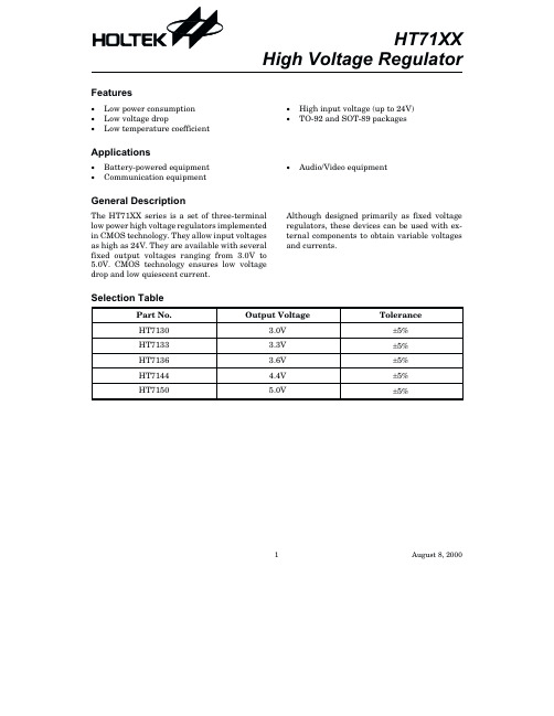
HT71XXHigh Voltage RegulatorSelection TablePart No.Output VoltageToleranceHT7130 3.0V ±5%HT7133 3.3V ±5%HT7136 3.6V ±5%HT7144 4.4V ±5%HT71505.0V±5%1August 8,2000Features·Low power consumption ·Low voltage drop·Low temperature coefficient·High input voltage (up to 24V)·TO-92and SOT-89packagesApplications·Battery-powered equipment ·Communication equipment·Audio/Video equipmentGeneral DescriptionThe HT71XX series is a set of three-terminal low power high voltage regulators implemented in CMOS technology.They allow input voltages as high as 24V.They are available with several fixed output voltages ranging from 3.0V to 5.0V.CMOS technology ensures low voltage drop and low quiescent current.Although designed primarily as fixed voltage regulators,these devices can be used with ex-ternal components to obtainvariable voltages and currents.Block DiagramPin AssignmentPad Assignment Pad CoordinatesUnit:m m Pad No.X Y 1-480.00-451.50287.50-444.503482.00-444.50Chip size:1374´1294(m m)2*The IC substrate should be connected to VDD in the PCB layout artwork.2August 8,2000Absolute Maximum RatingsSupply Voltage..............................-0.3V to28V Storage Temperature................-50°C to125°C Power Consumption.............................200mW Operating Temperature.................0°C to70°CNote:These are stress ratings only.Stresses exceeding the range specified under Absolute Maxi-mum Ratings may cause substantial damage to the device.Functional operation of this de-vice at other conditions beyond those listed in the specification is not implied and prolonged exposure to extreme conditions may affect device reliability.Electrical CharacteristicsHT7130,+3.0V output typeHT7133,+3.3V output type Ta=25°C3August8,2000HT7144,+4.4V output type Ta=25°C4August8,2000Application CircuitsBasic circuits5August8,2000High output current positive voltage regulatorShort-Circuit protection by Tr1Circuit for increasing output voltageV V (1+R2R1)I R2OUT XX SS =+HT71XX6August 8,2000Circuit for increasing output voltageV OUT=V XX+V D1 Constant current regulatorI VR IOUTXXA SS=+Dual supply7August8,20008August 8,2000Copyright Ó2000by HOLTEK SEMICONDUCTOR INC.The information appearing in this Data Sheet is believed to be accurate at the time of publication.However,Holtek assumes no responsibility arising from the use of the specifications described.The applications mentioned herein are used solely for the purpose of illustration and Holtek makes no warranty or representation that such applications will be suitable without further modification,nor recommends the use of its products for application that may pres-ent a risk to human life due to malfunction or otherwise.Holtek reserves the right to alter its products without prior notification.For the most up-to-date information,please visit our web site at .Holtek Semiconductor Inc.(Headquarters)No.3Creation Rd.II,Science-based Industrial Park,Hsinchu,Taiwan,R.O.C.Tel:886-3-563-1999Fax:886-3-563-1189Holtek Semiconductor Inc.(Taipei Office)5F,No.576,Sec.7Chung Hsiao E.Rd.,Taipei,Taiwan,R.O.C.Tel:886-2-2782-9635Fax:886-2-2782-9636Fax:886-2-2782-7128(International sales hotline)Holtek Semiconductor (Hong Kong)Ltd.RM.711,Tower 2,Cheung Sha Wan Plaza,833Cheung Sha Wan Rd.,Kowloon,Hong Kong Tel:852-2-745-8288Fax:852-2-742-8657。
5V稳压IC方案HT7050规格书

Rev. 1.4012014-03-19• 低功耗• 低温度系数• 高输入电压范围 (高达 30V)• 静态电流:3µA • 输出电压精度:±1%• 内建迟滞电路• 封装类型:TO92, SOT89 和 SOT23-5应用领域• 电池检测器• 电平选择器• 电源故障检测器• 微计算机复位• 电池存储备份• 非易失性RAM 信号存储保护概述HT70xxA-2系列是一组采用CMOS 技术实现的三端低功耗电压检测器。
该系列中的电压检测器能检测固定的电压,范围从 2.2V 到 8.2V 。
电压检测器系列由高精度低功耗的标准电压源、比较器、迟滞电路以及输出驱动器组成。
采用 CMOS 技术制造,因而确保了低功率消耗。
尽管主要用作固定电压检测器,但这些 IC 可搭配外部元件用于指定的阈值电压的检测。
选型表注:“xx ” 代表检测电压。
Rev. 1.4022014-03-19deN 沟道开漏输出(常开,低有效)输出表格和曲线图...d...引脚图电源供应电压 .............................................................................................................................V SS-0.3V ~ V SS+33V 输出电压 ...................................................................................................................................V SS-0.3V ~ V DD+0.3V 输出电流 .............................................................................................................................................................50mA功耗 ..................................................................................................................................................................200mW 储存温度范围 ............................................................................................................................................................−50°C ~ 125°C 工作环境温度 ........................................................................................................................................−40°C ~ 85°C 注:这里只强调额定功率,超过极限参数所规定的范围将对芯片造成损害,无法预期芯片在上述标示范围外的工作状态,而且若长期在标示范围外的条件下工作,可能影响芯片的可靠性。
HT7233 中文资料
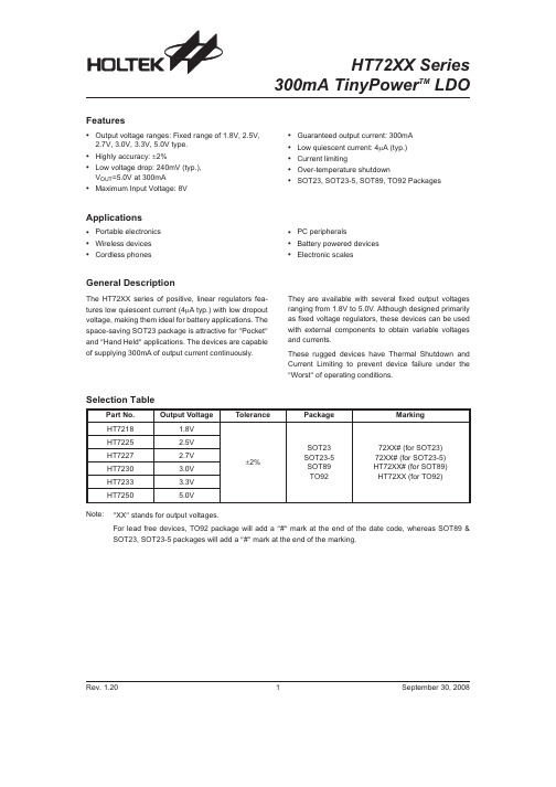
HT72XX Series300mA TinyPower TM LDOSelection TablePart No.Output VoltageTolerancePackageMarkingHT7218 1.8V ±2%SOT23SOT23-5SOT89TO9272XX#(for SOT23)72XX#(for SOT23-5)HT72XX#(for SOT89)HT72XX (for TO92)HT7225 2.5V HT7227 2.7V HT7230 3.0V HT7233 3.3V HT7250 5.0VNote:²XX ²stands for output voltages.For lead free devices,TO92package will add a ²#²mark at the end of the date code,whereas SOT89&SOT23,SOT23-5packages will add a ²#²mark at the end of the marking.Rev.1.201September 30,2008Features·Output voltage ranges:Fixed range of 1.8V,2.5V,2.7V,3.0V,3.3V,5.0V type.·Highly accuracy:±2%·Low voltage drop:240mV (typ.),V OUT =5.0V at 300mA·Maximum Input Voltage:8V·Guaranteed output current:300mA ·Low quiescent current:4m A (typ.)·Current limiting·Over-temperature shutdown·SOT23,SOT23-5,SOT89,TO92PackagesApplications·Portable electronics ·Wireless devices ·Cordless phones·PC peripherals·Battery powered devices ·Electronic scalesGeneral DescriptionThe HT72XX series of positive,linear regulators fea-tures low quiescent current (4m A typ.)with low dropout voltage,making them ideal for battery applications.The space-saving SOT23package is attractive for ²Pocket ²and ²Hand Held ²applications.The devices are capable of supplying 300mA of output current continuously.They are available with several fixed output voltages ranging from 1.8V to 5.0V.Although designed primarily as fixed voltage regulators,these devices can be used with external components to obtain variable voltages and currents.These rugged devices have Thermal Shutdown andCurrent Limiting to prevent device failure under the ²Worst ²of operating conditions.Block DiagramPin AssignmentPin DescriptionPin No.Pin Name Description SOT23SOT23-5SOT89TO92¾3¾¾CE Chip enable pin,high enable2533VOUT Output pin3122VIN Input pin1211GND Ground pin¾4¾¾NC No connectionAbsolute Maximum Ratings*Maximum Supply Voltage............................up to8.5V Storage Temperature...........................-50°C to125°C Operating Temperature..........................-40°C to85°CNote:These are stress ratings only.Stresses exceeding the range specified under²Absolute Maximum Ratings²may cause substantial damage to the device.Functional operation of this device at other conditions beyond those listed in the specification is not implied and prolonged exposure to extreme conditions may affect device reliability.²*²Absolute maximum ratings indicate limits beyond which damage to the device may occur.Operating Ratings in-dicate conditions for which the device is intended to be functional,but do not guarantee specific performance limits.The guaranteed specifications apply only for the test conditions listed.Rev.1.202September30,2008Thermal InformationSymbol Parameter Package Max.Unitq JA Thermal Resistance(Junction to Ambient)(Assume no ambient airflow,no heat sink)SOT23667°C/WSOT23-5500°C/WSOT89200°C/WTO92200°C/WP D Power DissipationSOT230.15W SOT23-50.20W SOT890.50W TO920.50WNote:P D is measured at Ta=25°CElectrical Characteristics Tj=25°C,V IN=V OUT+1.0V,I O=1mA,unless otherwise specified Symbol Parameter Test Conditions Min.Typ.Max.UnitV IN Input Voltage¾¾¾8VD V OUT Output Voltage Tolerance¾-2¾2%I SS Quiescent Current I O=0mA,V CE=V IN¾47m AD V LOAD Load Regulation(Note1)1mA£I OUT£300mA¾0.0040.008%/mAV DROP Dropout Voltage(Note2)D V OUT=2%I OUT=300mAV O£1.8V¾8001200mV2.5V£V O£2.7V¾3504003.0V£V O£5.0V¾240300D V LINE Line Regulation V OUT+1.0V£V IN£8.0V¾0.20.3%/VI LIM Current Limit(Note3)D V OUT=10%300¾¾mAV IH CE Input High Threshold V OUT+1V£V IN£8V 2.0¾¾VV IL CE Input Low Threshold V OUT+1V£V IN£8V¾¾0.8VI SD Shutdown Current CE input voltage£0.8V¾0.51m ATemperature Coefficient-40°C<Ta<85°C¾±0.8¾mV/°C Note: 1.Load regulation is measured at a constant junction temperature,using pulse testing with a low ON time and is guaranteed up to the maximum power dissipation.Power dissipation is determined by the input/outputdifferential voltage and the output current.Guaranteed maximum power dissipation will not be available over the full input/output range.The maximum allowable power dissipation at any ambient temperature isP D=(T J(MAX)-Ta)/q JA.2.Dropout voltage is defined as the input voltage minus the output voltage that produces a2%change in theoutput voltage from the value at V IN=V OUT+1V with a fixed load.3.Current limit is measured by pulsing for a short time.Rev.1.203September30,2008Application CircuitsBasic CircuitsTypical Application Circuits·High output current positive voltage regulatorRev.1.204September30,2008·Increased Output voltage CircuitV=V(1+R2R1)+I R2OUT XX SS ·Dual Supply CircuitV=V+VOUT1XX2XX1V=VOUT2XX2·Tracking Voltage Regulator-V=V x R RO OUT B ARev.1.205September30,2008Package Information3-pin SOT23Outline DimensionsSymbolDimensions in mmMin.Nom.Max.A 1.0¾ 1.3A1¾¾0.1A20.7¾0.9b0.35¾0.5C0.10¾0.25D 2.7¾ 3.1E 1.4¾ 1.8e¾ 1.9¾H 2.6¾ 3.0L0.37¾¾q1°¾9°Rev.1.206September30,2008SymbolDimensions in mmMin.Nom.Max.A 1.00¾ 1.30A1¾¾0.10A20.70¾0.90b0.35¾0.50C0.10¾0.25D 2.70¾ 3.10E 1.40¾ 1.80e¾ 1.90¾H 2.6¾ 3.0L0.37¾¾q1°¾9°Rev.1.207September30,2008SymbolDimensions in milMin.Nom.Max.A173¾181B59¾72C90¾102D35¾47E155¾167F14¾19G17¾22H¾59¾I55¾63J14¾17Rev.1.208September30,2008SymbolDimensions in milMin.Nom.Max.A170¾200B170¾200C500¾¾D11¾20E90¾110F45¾55G45¾65H130¾160I8¾18a4°¾6°Rev.1.209September30,2008Product Tape and Reel SpecificationsReel DimensionsSOT23,SOT23-5Symbol Description Dimensions in mmA Reel Outer Diameter178.0±1.0B Reel Inner Diameter62.0±1.0C Spindle Hole Diameter13.0±0.2D Key Slit Width 2.50±0.25T1Space Between Flange8.4+1.5/-0.0T2Reel Thickness11.4+1.5/-0.0SOT89Symbol Description Dimensions in mmA Reel Outer Diameter180.0±1.0B Reel Inner Diameter62.0±1.5C Spindle Hole Diameter12.75+0.15/-0.00D Key Slit Width 1.90±0.15T1Space Between Flange12.4+0.2/-0.00T2Reel Thickness17.0+0.0/-0.4Rev.1.2010September30,20083-pin TO92Reel Dimensions(Unit:mm)Rev.1.2011September30,2008Carrier Tape DimensionsSOT23,SOT23-5Symbol Description Dimensions in mm W Carrier Tape Width8.0±0.3P Cavity Pitch 4.0±0.1E Perforation Position 1.75±0.10F Cavity to Perforation(Width Direction) 3.50±0.05D Perforation Diameter 1.5+0.1/-0.0D1Cavity Hole Diameter 1.5+0.1/-0.0P0Perforation Pitch 4.0±0.1P1Cavity to Perforation(Length Direction) 2.00±0.05A0Cavity Length 3.15±0.10B0Cavity Width 3.2±0.1K0Cavity Depth 1.4±0.1t Carrier Tape Thickness0.20±0.03C Cover Tape Width 5.3±0.1SOT89Symbol Description Dimensions in mm W Carrier Tape Width12.0+0.3/-0.1P Cavity Pitch8.0±0.1E Perforation Position 1.75±0.10F Cavity to Perforation(Width Direction) 5.50±0.05D Perforation Diameter 1.5+0.1/-0.0D1Cavity Hole Diameter 1.5+0.1/-0.0P0Perforation Pitch 4.0±0.1P1Cavity to Perforation(Length Direction) 2.0±0.1A0Cavity Length 4.8±0.1B0Cavity Width 4.5±0.1K0Cavity Depth 1.8±0.1t Carrier Tape Thickness0.300±0.013C Cover Tape Width9.3±0.1Rev.1.2012September30,20083-pin TO92Carrier Tape DimensionsTO92Symbol Description Dimensions in mm I1Taped Lead Length(2.5)P Component Pitch12.7±1.0P0Perforation Pitch12.7±0.3P2Component to Perforation(Length Direction) 6.35±0.40F1Lead Spread 2.5+0.4/-0.1F2Lead Spread 2.5+0.4/-0.1D h Component Alignment0.0±0.1W Carrier Tape Width18.0+1.0/-0.5W0Hold-down Tape Width 6.0±0.5W1Perforation Position9.0±0.5W2Hold-down Tape Position(0.5)H0Lead Clinch Height16.0±0.5H1Component Height Less than24.7D0Perforation Diameter 4.0±0.2t Taped Lead Thickness0.7±0.2H Component Base Height19.0±0.5Note:Thickness less than0.38±0.05mm~0.5mmP0Accumulated pitch tolerance:±1mm/20pitches.()Bracketed figures are for consultation onlyRev.1.2013September30,2008CopyrightÓ2008by HOLTEK SEMICONDUCTOR INC.The information appearing in this Data Sheet is believed to be accurate at the time of publication.However,Holtek as-sumes no responsibility arising from the use of the specifications described.The applications mentioned herein are used solely for the purpose of illustration and Holtek makes no warranty or representation that such applications will be suitable without further modification,nor recommends the use of its products for application that may present a risk to human life due to malfunction or otherwise.Holtek¢s products are not authorized for use as critical components in life support devices or systems.Holtek reserves the right to alter its products without prior notification.For the most up-to-date information, please visit our web site at .Rev.1.2014September30,2008。
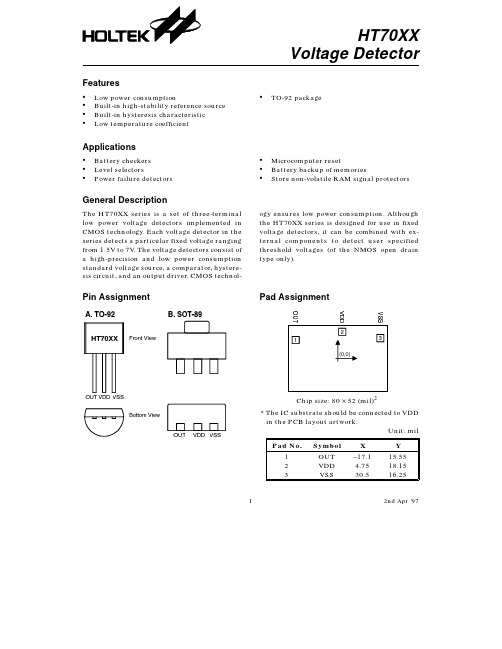
HT70XX
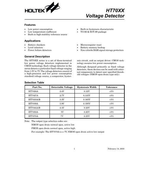
HT70XXVoltage DetectorSelection TablePart No.Detectable VoltageHysteresis WidthToleranceHT7024A 2.4V 0.12V ±5%HT7027A 2.7V 0.135V ±5%HT7033A/B 3.3V 0.165V ±5%HT7039A 3.9V 0.195V ±5%HT7044A/B 4.4V 0.22V ±5%HT7050A 5V 0.25V ±5%HT7070A7V0.35V±5%Note:The output type selection codes are:NMOS open drain normal open,active low PMOS open drain normal open,active highFor example:The HT7070A is a 7V ,NMOS open drain active low output1February 14,2000General DescriptionThe HT70XX series is a set of three-terminal low power voltage detectors implemented in CMOS technology.Each voltage detector in the series detects a particular fixed voltage ranging from 1.5V to 7V .The voltage detectors consist of a high-precision and low power consumption standard voltage source,a comparator,hyster-esis circuit,and an output driver.CMOS tech-nology ensures low power consumption.Although designed primarily as fixed voltage detectors,these devices can be used with exter-nal components to detect user specified thresh-old voltages (NMOS open drain type only).Features·Low power consumption ·Low temperature coefficient·Built-in high-stability reference source·Built-in hysteresis characteristic ·TO-92&SOT-89packageApplications·Batterycheckers ·Level selectors·Power failure detectors ·Microcomputer reset ·Battery memory backup·Non-volatile RAM signal storage protectorsOutput type selection tableV DDV DD >V DET (+)V DD £V DET (-)TypeV OUT A Hi-Z VSS BHi-ZVDDBlock DiagramN channel open drain output (normal open;active low)A type2February 14,2000P channel open drain output(normal open;active high)B type3February14,2000Pin Assignment Pad AssignmentChip size:1317´1158(m m)2*The IC substrate should be connected to VDD inthe PCB layout artwork.Pad Coordinates Unit:m mPad No.X Y1-483.30-379.502-234.60-399.503443.90-386.00Absolute Maximum RatingsSupply Voltage...............................-0.3V to26V Output Current.........................................50mA Output Voltage..............V SS-0.3V to V DD+0.3V Storage Temperature.................-50°C to125°C Power Consumption...............................200mW Operating Temperature..................0°C to70°C Note:These are stress ratings only.Stresses exceeding the range specified under²Absolute Maxi-mum Ratings²may cause substantial damage to the device.Functional operation of this de-vice at other conditions beyond those listed in the specification is not implied and prolonged exposure to extreme conditions may affect device reliability.4February14,2000Electrical CharacteristicsHT7024A Ta=25°CHT7027A Ta=25°C5February14,2000Note:HT7033A has no I OHHT7033B has no I OLHT7039A Ta=25°C6February14,2000Note:HT7044A has no I OHHT7044B has no I OLHT7050A Ta=25°C7February14,20008February 14,2000Functional DescriptionThe HT70XX series is a set of voltage detectors equipped with a high stability voltage reference which is connected to the negative input of a comparator ¾denoted as V REF in the following figure for NMOS output voltage detector.When the voltage drop to the positive input of the comparator (i,e,V B )is higher than V REF ,VOUT goes high,M1turns off,and V B is ex-pressed as V BH =VDD ´(RB+RC)/(RA+RB+RC).If VDD is decreased so that V B falls to a value less than V REF ,the comparator output inverts from high to low,VOUT goes low,V C is high,M1turns on,RC is bypassed,and V B becomes:V BL =VDD ´RB/(RA+RB),which is less than V BH.By so doing,the comparator output will stay low to prevent the circuit from oscillating when V B »V REF.If VDD falls below the minimum operating volt-age,the output becomes undefined.When VDD goes from low to VDD ´RB/(RA+RB)>V REF ,the comparator output and VOUT goes high.The detectable voltage is defined as:V DET (-)=RA RB RCRB RC +++´V REFThe release voltage is defined as:V DET (+)=RA RBRB+´V REFThe hysteresis width is:V HYS =V DET (+)-V DET (-)The figure demonstrates the NMOS output type with positive output polarity (VOUT is normally open,active low).The HT70XX seriesalso supplies options for other output types with active high outputs.Application circuits shown are examples of positive output polarity (normally open,active low)unless otherwise specified.NMOS output voltage detector (HT70XXA)Application CircuitsMicrocomputer reset circuitNormally a reset circuit is required to protect the microcomputer system from malfunctions due to power line interruptions.The following examples show how different output configura-tions perform a reset function in various sys-tems.·NMOS open drain output application for separate power supply·NMOS open drain output application with R-C delay Power-on reset circuitWith several external components,the NMOS open drain type of the HT70XX series can be used to perform a power-on reset function as shown:9February14,20005V power line monitoring circuit Generally,a minimum operating voltage of 4.5V is guaranteed in a5V power line system. The HT7044A is recommended for use as5V power line monitoring circuit.·5V power line monitor with power-on reset ·with5V voltage regulator Change of detectable voltageIf the required voltage is not found in the stan-dard product selection table,it is possible to change it by using external resistance dividers or diodes.·Varying the detectable voltage with a resis-tance dividerDetectable voltage=RA RBRB+´VDETHysteresis width=RA RBRB+´VHYS ·Varying the detectable voltage with a diodeDetectable Voltage=V f1+V f2+V DET10February14,2000Malfunction analysisThe following circuit demonstrates the way a circuit analyzes malfunctions by monitoring the variation or spike noise of power supply voltage.Charge monitoring circuitThe following circuit shows a charged monitor for protection against battery deterioration by overcharging.When the voltage of the battery is higher than the set detectable voltage,the transistor turns on to bypass the charge cur-rent,protecting the battery from overcharging.Battery backup for memoriesAn application example of battery backup for memory data retention is shown below.During battery backup(VDD below detectable voltage),the HT70XXB output goes high to disable the chip select de-11February14,2000Level selectorThe following diagram illustrates a logic level selector.12February14,200013February 14,2000Copyright Ó2000by HOLTEK SEMICONDUCTOR INC.The information appearing in this Data Sheet is believed to be accurate at the time of publication.However,Holtek assumes no responsibility arising from the use of the specifications described.The applications mentioned herein are used solely for the purpose of illustration and Holtek makes no warranty or representation that such applications will be suitable without further modification,nor recommends the use of its products for application that may pres-ent a risk to human life due to malfunction or otherwise.Holtek reserves the right to alter its products without prior notification.For the most up-to-date information,please visit our web site at .Holtek Semiconductor Inc.(Headquarters)No.3Creation Rd.II,Science-based Industrial Park,Hsinchu,Taiwan,R.O.C.Tel:886-3-563-1999Fax:886-3-563-1189Holtek Semiconductor Inc.(Taipei Office)5F,No.576,Sec.7Chung Hsiao E.Rd.,Taipei,Taiwan,R.O.C.Tel:886-2-2782-9635Fax:886-2-2782-9636Fax:886-2-2782-7128(International sales hotline)Holtek Semiconductor (Hong Kong)Ltd.RM.711,Tower 2,Cheung Sha Wan Plaza,833Cheung Sha Wan Rd.,Kowloon,Hong Kong Tel:852-2-745-8288Fax:852-2-742-8657。
HT7033a规格书
Rev. 2.1012014-03-19• 低功耗• 低温度系数• 高输入电压范围 (高达 30V)• 静态电流:3µA • 输出电压精度:±3%• 内建迟滞电路• 封装类型:TO92, SOT89, SOT23和 SOT23-5应用领域• 电池检测器• 电平选择器• 电源故障检测器• 微计算机复位• 电池存储备份• 非易失性RAM 信号存储保护HT70xxA-1系列是一组采用CMOS 技术实现的三端低功耗电压检测器。
该系列中的电压检测器能检测固定的电压,范围从 2.2V 到 5.0V 。
电压检测器系列由高精度低功耗的标准电压源、比较器、迟滞电路以及输出驱动器组成。
采用 CMOS 技术制造,因而确保了低功率消耗。
尽管主要用作固定电压检测器,但这些 IC 可搭配外部元件用于指定的阈值电压的检测。
选型表注:“xx ” 代表检测电压。
Rev. 2.1022014-03-19N 沟道开漏输出(常开,低有效)输出表格和曲线图..引脚图电源供应电压 ..............................V SS-0.3V ~ V SS+33V 输出电压 ....................................V SS-0.3V ~ V DD+0.3V 输出电流 ..............................................................50mA 功耗 ..................................................................200mW 储存温度范围 .................................................−50°C ~ 125°C 工作环境温度 .........................................−40°C ~ 85°C注:这里只强调额定功率,超过极限参数所规定的范围将对芯片造成损害,无法预期芯片在上述标示范围外的工作状态,而且若长期在标示范围外的条件下工作,可能影响芯片的可靠性。
低电压检测电路说明
HT70xxA-2TinyPower TM Voltage DetectorSelection TableNote:²xx ²stands for output voltages.Both lead free and green compound devices are available.Note the symbol marks below:²#²stands for lead free devices.²+²stands for green compound devices,which are Lead-free and Halogen-free.For the TO92package,the symbol mark will be at the end of the date code.Whereas for the SOT89and SOT23-5,the symbol mask will be located at the end of IC marking.Rev.1.201December 14,2012General DescriptionThe HT70xxA-2series devices area set of three terminal low power voltage detectors implemented in CMOS technology.Each voltage detector in the series detects a particular fixed voltage ranging from 2.2V to 8.2V.The voltage detectors consist of a high-precision and low power consumption standard voltage source as well as acomparator,hysteresis circuit,and an output driver.CMOS technology ensures low power consumption.Although designed primarily as fixed voltage detectors,these devices can be used with external components to detect user specified threshold voltages.Features·Low power consumption ·Low temperature coefficient·High input voltage range (up to 24V)·Output voltage accuracy:tolerance ±1%·Built-in hysteresis characteristic ·TO92,SOT89and SOT23-5packageApplications·Battery checkers ·Level selectors ·Power failure detectors·Microcomputer reset ·Battery memory backup·Non-volatile RAM signal storage protectorsBlock DiagramN Channel Open Drain Output(Normal Open;Active Low)Output Table&CurvePin AssignmentRev.1.202December14,2012Absolute Maximum RatingsSupply Voltage.............................................................................................................................V SS-0.3V to V SS+26V Output Voltage...........................V SS-0.3V to V DD+0.3V Output Current......................................................50mA Storage Temperature............................-50°C to125°C Power Consumption..........................................200mW Operating Temperature...........................-40°C to85°CNote:These are stress ratings only.Stresses exceeding the range specified under²Absolute Maximum Ratings²may cause substantial damage to the device.Functional operation of this device at other conditions beyond those listed in the specification is not implied and prolonged exposure to extreme conditions may affect device reliability.Electrical CharacteristicsHT7022A-2Ta=25°CHT7024A-2Ta=25°CRev.1.203December14,2012HT7033A-2Ta=25°CHT7039A-2Ta=25°CRev.1.204December14,2012HT7050A-2Ta=25°CHT7082A-2Ta=25°CRev.1.205December14,2012Functional DescriptionThe HT70xxA-2series is a set of voltage detectors equipped with a high stability voltage reference which is connected to the negative input of a comparator¾denoted as V REF in the following figure for NMOS output voltage detector.When the voltage drop to the positive input of the comparator(i,e,V B)is higher than V REF,VOUT goes high,M1turns off,and V B is expressed as V BH=V DD´(R B+R C)/(R A+R B+R C).If V DD is decreased so that V B falls to a value less than V REF,the comparator output inverts from high to low,V OUT goes low,V C is high,M1 turns on,RC is bypassed,and V B becomes:V BL=V DD´R B/(R A+R B),which is less than V BH.By so doing,the comparator output will stay low to prevent the circuit from oscillating when V B»V REF.If V DD falls below the minimum operating voltage,the output becomes undefined.When VDD goes from low to V DD´R B/(R A+R B)>V REF,the comparator output and V OUT goes high.The detectable voltage is defined as:V DET(-)=R+R+RR+RA B CB C´V REFThe release voltage is defined as:V DET(+)=R+RRA BB´V REFThe hysteresis width is:V HYS=V DET(+)-V DET(-)The figure demonstrates the NMOS output type withpositive output polarity(V OUT is normally open,activelow).The HT70xxA-2series also supplies options forother output types with active high outputs.Applicationcircuits shown are examples of positive output polarity(normally open,active low)unless otherwise specified.NMOS Output Voltage DetectorRev.1.206December14,2012Application CircuitsRev.1.207December 14,2012Microcomputer Reset CircuitNormally a reset circuit is required to protect the microcomputer system from malfunctions due to power line interruptions.The following examples show how different output configurations perform a reset function in various systems.·NMOS open drain output application for separatepower supply·NMOS open drain output application with R-C delayPower-on Reset CircuitWith several external components,the NMOS open drain type of the HT70xxA-2series can be used to perform a power-on reset function as shown:5V Power Line Monitoring CircuitGenerally,a minimum operating voltage of 4.5V is guaranteed in a 5V power line system.The HT7044A-2is recommended for use as 5V power line monitoring circuit.·5V power line monitor with power-on reset·with5V voltage regulatorChange of Detectable VoltageIf the required voltage is not found in the standard product selection table,it is possible to change it by using external resistance dividers or diodes.·Varying the detectable voltage with a resistance di-viderDetectable voltage=R+RRA BB´V DETHysteresis width=R+RRA BB´V HYS·Varying the detectable voltage with a diode Detectable Voltage=V f1+V f2+V DET Malfunction AnalysisThe following circuit demonstrates the way a circuit analyzes malfunctions by monitoring the variation or spike noise of power supply voltage.Charge Monitoring CircuitThe following circuit shows a charged monitor for protection against battery deterioration by overcharging.When the voltage of the battery is higher than the set detectable voltage,the transistor turns on to bypass the charge current,protecting the battery from overcharging.Rev.1.208December14,2012Level SelectorThe following diagram illustrates a logic level selector.Rev.1.209December14,2012Package InformationNote that the package information provided here is for consultation purposes only.As this information may be updated at regular intervals users are reminded to consult the Holtek website(/english/literature/package.pdf)for the latest version of the package information.3-pin TO92Outline DimensionsRev.1.2010December14,2012Rev.1.2011December14,2012Rev.1.2012December14,2012Product Tape and Reel SpecificationsTO92Reel Dimensions(Unit:mm)Rev.1.2013December14,2012Reel DimensionsSOT89-3Rev.1.2014December14,2012Note:Thickness less than0.38±0.05mm~0.5mmP0Accumulated pitch tolerance:±1mm/20pitches.()Bracketed figures are for consultation onlyRev.1.2015December14,2012SOT89-3Rev.1.2016December14,2012Holtek Semiconductor Inc.(Headquarters)No.3,Creation Rd.II,Science Park,Hsinchu,TaiwanTel:886-3-563-1999Fax:886-3-563-1189Holtek Semiconductor Inc.(Taipei Sales Office)4F-2,No.3-2,YuanQu St.,Nankang Software Park,Taipei115,TaiwanTel:886-2-2655-7070Fax:886-2-2655-7373Fax:886-2-2655-7383(International sales hotline)Holtek Semiconductor(China)Inc.Building No.10,Xinzhu Court,(No.1Headquarters),4Cuizhu Road,Songshan Lake,Dongguan,China523808Tel:86-769-2626-1300Fax:86-769-2626-1311Holtek Semiconductor(USA),Inc.(North America Sales Office)46729Fremont Blvd.,Fremont,CA94538,USATel:1-510-252-9880Fax:1-510-252-9885CopyrightÓ2012by HOLTEK SEMICONDUCTOR INC.The information appearing in this Data Sheet is believed to be accurate at the time of publication.However,Holtek as-sumes no responsibility arising from the use of the specifications described.The applications mentioned herein are used solely for the purpose of illustration and Holtek makes no warranty or representation that such applications will be suitable without further modification,nor recommends the use of its products for application that may present a risk to human life due to malfunction or otherwise.Holtek¢s products are not authorized for use as critical components in life support devices or systems.Holtek reserves the right to alter its products without prior notification.For the most up-to-date information, please visit our web site at .Rev.1.2017December14,2012。
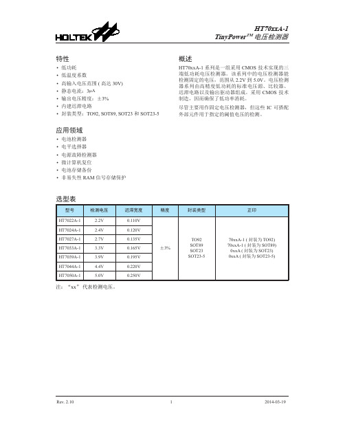
HT70系列微功耗电压检测中文资料
广州周立功单片机发展有限公司 Tel 020 38730976 38730916 Fax 38730925
电气特性
HT7022A 表 3-1
符号
参数
VDET
VHYS IDD VDD IOL VDET
TA
高-低可检测电压 低-高可检测电压
滞后度 运行电流 运行电压 输出灌电流
保了低功耗 尽管检测器主要是设计成固定电压的检测 但通过外围元件也能检测用户所指定的阀值电压
仅限 NMOS 开漏类型
选择表 1
型号
可检测电压
滞后度
允差
HT7022A
2.2V
0.11V
5%
HT7024A
2.4V
0.12V
5%
HT7027A
2.7V
0.135V
5%
HT7033A
3.3V
0.165V
5%
HT7039A
图 1-10
5V 电源监视电路 一般地 5V 电源系统的运行电压最低为 4.5V HT7044A 可用作 5V 电源的监视电路 带上电复位的 5V 电源监视器
带 5V 电压调整器的电源监视器
图 1-11
图 1-12 -8-
广州周立功单片机发展有限公司 Tel 020 38730976 38730916 Fax 38730925
可检测电压表示为
VREF
VDET - = RA+RB+RC / RB+RC 释放电压表示为
VREF
VDET + = RA+RB /RB VREF 滞后度为 VHYS=VDET + -VDET 此图所示为带正极性输出的 NMOS 输出类型 VOUT 是常开 低有效 的高有效输出 除有其它说明 这里的应用电路都是指正极性输出 常开
HT70XX(HOLTEK)
HT70XXVoltage DetectorPin Assignment Pad AssignmentChip size: 80 × 52 (mil)2* The IC substrate should be connected to VDD in the PCB layout artwork.Unit: milGeneral DescriptionThe HT70XX series is a set of three-terminal low power voltage detectors implemented in CMOS technology . Each voltage detector in the series detects a particular fixed voltage ranging from 1.5V to 7V . The voltage detectors consist of a high-precision and low power consumption standard voltage source, a comparator, hystere-sis circuit, and an output driver. CMOS technol-ogy ensures low power consumption. Although the HT70XX series is designed for use in fixed voltage detectors, it can be combined with ex-ternal components to detect user specified threshold voltages (of the NMOS open drain type only).Features•Low power consumption•Built-in high-stability reference source •Built-in hysteresis characteristic •Low temperature coefficient•TO-92 packageApplications•Battery checkers •Level selectors•Power failure detectors •Microcomputer reset•Battery backup of memories•Store non-volatile RAM signal protectorsBlock DiagramN channel open drain output (normal open; active low)P channel open drain output (normal open; active high)CMOS output (normal hign, active low)Selection GuideNote: The output type selection codes are:NMOS open drain normal open, active low.PMOS open drain normal open, active high.For example: The HT7070A is a 7V, NMOS open drain active low output.Absolute Maximum RatingsSupply Voltage...............................–0.3V to 26V Output Current..........................................50mA Output Voltage..............V SS–0.3V to V DD+0.3V Storage Temperature.................–50°C to 125°C Power Dissipation....................................200mΩOperating Temperature...................0°C to 70°CElectrical CharacteristicsNote:The HT7024A has no I OH.The HT7024B has no I OL.Note:The HT7027A has no I OH.The HT7027B has no I OL.42nd Apr ’97Note:The HT7033A has no I OH.The HT7033B has no I OL.Note:The HT7039A has no I OH.The HT7039B has no I OL.52nd Apr ’97Note:The HT7044A has no I OH.The HT7044B has no I OL.Note:The HT7050A has no I OH.The HT7050B has no I OL.62nd Apr ’97Note:The HT7070A has no I OH.The HT7070B has no I OL.72nd Apr ’97Fig. 1 NMOS output voltage detector (HT70XXA)Functional DescriptionThe HT70XX series is a set of voltage detectors equipped with a high stability voltage reference which is connected to the negative input of a comparator — denoted as V REF in the following figure (Fig. 1).When the voltage drop to the positive input of the comparator (i,e,V B ) is higher than V REF ,VOUT goes high, M1 turns off, and V B is ex-pressed as V BH =VDD ∗(RB+RC) / (RA+RB+RC).If VDD is decreased so that V B falls to a value that is less than V REF , the comparator output inverts (from high to low), VOUT goes low, V C is high, M1 turns on, RC is bypassed, and V B becomes: V BL =VDD ∗RB / (RA+RB), which is less than V BH. By so doing the comparator out-put will stay low to prevent the circuit from oscillating when V B ≈ V REF .If VDD falls bellow the minimum operating voltage, the output becomes undefined. When VDD goes from low to VDD ∗RB / (RA+RB) >VREF , the comparator output goes high andVOUT goes high again.The detection voltage is as defined:V DET (–) =RA +RB +RCRB +RC∗ V REFThe release voltage is as defined:V DET (+) =RA +RBRB∗ V REF The hysteresis width is:V HYS = V DET (+) – V DET (–)Figure 1 demonstrates the NMOS output type with positive output polarity (VOUT is nor-mally open, active low). The HT70XX series also supplies options for other output types with active high outputs. Application circuits shown in the next paragraph are examples of positive output polarity (normally open, active low) un-less otherwise specified.Application CircuitMicro-computer reset circuitNormally a reset circuit is required to protect the microcomputer system from malfunctions that are caused by power line interruptions.The following examples show how that different output configurations perform a reset function in various systems.•NMOS open drain output application forseparate power supply•NMOS open drain output application withR-C delayPower-on reset circuitWith several external components, the NMOS open drain type of the HT70XX series can be used to perform a power-on reset function asshown:HT70XX92nd Apr ’975V power line monitoring circuit Generally , a minimum operating voltage of 4.5V is guaranteed in a 5V power line system. The HT7044A is recommended to be used as moni-toring circuit for a 5V power line.•5V power line monitor with power-on reset•with a 5V voltage regulatorChange of detection voltageIf the required detection voltage cannot be found in the standard product selection table, it is possible to change the detection voltage by using external resistance dividers or diodes.•Varying the detection voltage with a resis-tance dividerDetection voltage = RA +RBRB∗ V DET Hysteresis width =RA +RBRB∗ V HYS •Varying the detection voltage with a diodeDetection Voltage = V f1+V f2+VDETMalfunction analysisThe following circuit demonstrates the way thata circuit analyzes malfunctions by monitoringthe variation or spike noise of power supplyvoltage.Charge monitoring circuitThe following circuit shows a charge monitor forprotection against battery deterioration byovercharging. When the voltage of the batteryis higher than the set detection voltage, thetransistor turns on to bypass the charge cur-rent, protecting the battery from overcharging.Level selectorThe following diagram illustrates a logic level selector.Package InformationTO-92HT70XX132nd Apr ’97TO-89 OutlineHT70XX142nd Apr ’97。
HT7133规格书
4.268 4.400 4.532
V
IOUT
输出电流
6.4V
—
20
30
—
mA
∆ VOUT
负载调整率
6.4V 1mA ≤ IOUT ≤ 30mA
—
15
45
mV
VDIF
压降 ( 注 )
— IOUT=1mA, ∆ VOUT=2%
—
35
55
mV
ISS
D V OUT D V IN ´ V O U T
耗电流 输入电压调节率
Ta=25°C 单位
VOUT
输出电压
5.6V IOUT=10mA
3.492 3.600 3.708
V
IOUT
输出电流
5.6V
—
20
30
—
mA
∆ VOUT
VDIF
ISS
D V OUT D V IN ´ V O U T
VIN
D V OUT D T a´ V O U T
负载调整率 压降 ( 注 ) 耗电流 输入电压调节率 输入电压 温度系数
—
35
100
mV
ISS
D V OUT D V IN ´ V O U T
耗电流 输入电压调节率
4.5V 无负载
—
2.5
4.0
— 3.5V ≤ VIN ≤ 30V, IOUT=1mA
—
0.1
0.2
µA %/V
VIN
输入电压
—
—
—
—
30
V
D V OUT D T a´ V O U T
温度系数
4.5V IOUT=10mA, -40°C<Ta<85°C
HT7070A

HT70XXVoltage DetectorSelection TablePart No.Detectable VoltageHysteresis WidthTolerance HT7022A 2.2V 0.11V ±5%HT7024A 2.4V 0.12V ±5%HT7027A 2.7V 0.135V ±5%HT7033A 3.3V 0.165V ±5%HT7039A 3.9V 0.195V ±5%HT7044A 4.4V 0.22V ±5%HT7050A 5.0V 0.25V ±5%HT7070A 7.0V0.35V±5%Note:The output type selection codes are:NMOS open drain normal open,active lowFor example:The HT7070A is a 7.0V,NMOS open drain active low outputOutput type selection tableV DDV DD >V DET (+)V DD £V DET (-)TypeV OUT AHi-ZVSSRev.1.601January 14,2003General DescriptionThe HT70XX series is a set of three-terminal low power voltage detectors implemented in CMOS technology.Each voltage detector in the series detects a particular fixed voltage ranging from 2.2V to 7V.The voltage de-tectors consist of a high-precision and low power con-sumption standard voltage source,a comparator,hysteresis circuit,and an output driver.CMOS technol-ogy ensures low power consumption.Although designed primarily as fixed voltage detectors,these devices can be used with external components to detect user specified threshold voltages (NMOS open drain type only).Features·Low power consumption ·Low temperature coefficient·Built-in high-stability reference source·Built-in hysteresis characteristic ·TO-92&SOT-89packageApplications·Battery checkers ·Level selectors ·Power failure detectors·Microcomputer reset ·Battery memory backup·Non-volatile RAM signal storage protectorsBlock DiagramN channel open drain output(normal open;active low)A typePin AssignmentRev.1.602January14,2003Pad AssignmentHT70XX (except HT7022A)Chip size:1317´1158(m m)2*The IC substrate should be connected to VDD in the PCB layout artwork.HT7022A onlyChip size:2032´1321(m m)2*The IC substrate should be connected to VDD in the PCB layout artwork.Absolute Maximum RatingsSupply Voltage,except HT7022A..................................................................................................V SS -0.3V to V SS +26V Supply Voltage,HT7022A only....................................................................................................................-0.3V to13V Output Voltage...........................V SS -0.3V to V DD +0.3V Output Current......................................................50mA Storage Temperature............................-50°C to 125°C Power Consumption..........................................200mWOperating Temperature 0°C to 70°CNote:These are stress ratings only.Stresses exceeding the range specified under ²Absolute Maximum Ratings ²maycause substantial damage to the device.Functional operation of this device at other conditions beyond those listed in the specification is not implied and prolonged exposure to extreme conditions may affect device reliabil-ity.Rev.1.603January 14,2003Pad CoordinatesHT70XX (except HT7022A)Unit:m m Pad No.X Y 1-483.30-379.502-234.60-399.503443.90-386.00HT7022A onlyUnit:m mPad No.X Y1-434.34394.972120.65461.013774.70412.75Electrical CharacteristicsHT7022A Ta=25°CHT7024A Ta=25°CHT7027A Ta=25°CRev.1.604January14,2003HT7039A Ta=25°CHT7044A Ta=25°CRev.1.605January14,2003HT7070A Ta=25°CRev.1.606January 14,2003Functional DescriptionThe HT70XX series is a set of voltage detectors equipped with a high stability voltage reference which is connected to the negative input of a comparator ¾de-noted as V REF in the following figure for NMOS output voltage detector.When the voltage drop to the positive input of the com-parator (i,e,V B )is higher than V REF ,VOUT goes high,M1turns off,and V B is expressed as V BH =V DD ´(R B +R C )/(R A +R B +R C ).If V DD is decreased so that V B falls to a value less than V REF ,the comparator output in-verts from high to low,V OUT goes low,V C is high,M1turns on,RC is bypassed,and V B becomes:V BL =V DD ´R B /(R A +R B ),which is less than V BH.By so doing,the comparator output will stay low to prevent the circuit from oscillating when V B »V REF.If V DD falls below the minimum operating voltage,the output becomes undefined.When VDD goes from low to V DD ´R B /(R A +R B )>V REF ,the comparator output and V OUT goes high.The detectable voltage is defined as:V DET (-)=R R R R R A B CB C +++´V REFThe release voltage is defined as:V DET (+)=R R R A BB+´V REFThe hysteresis width is:V HYS=V DET(+)-V DET(-)The figure demonstrates the NMOS output type withpositive output polarity(V OUT is normally open,activelow).The HT70XX series also supplies options for otheroutput types with active high outputs.Application cir-cuits shown are examples of positive output polarity(normally open,active low)unless otherwise specified.NMOS output voltage detector(HT70XXA) Application CircuitsMicrocomputer reset circuitNormally a reset circuit is required to protect the micro-computer system from malfunctions due to power line interruptions.The following examples show how differ-ent output configurations perform a reset function in var-ious systems.·NMOS open drain output application for separate power supply·NMOS open drain output application with R-C delayPower-on reset circuitWith several external components,the NMOS open drain type of the HT70XX series can be used to perform a power-on reset function as shown:Rev.1.607January14,20035V power line monitoring circuitGenerally,a minimum operating voltage of4.5V is guar-anteed in a5V power line system.The HT7044A is rec-ommended for use as5V power line monitoring circuit.·5V power line monitor with power-on reset·with5V voltage regulatorChange of detectable voltageIf the required voltage is not found in the standard prod-uct selection table,it is possible to change it by using ex-ternal resistance dividers or diodes.·Varying the detectable voltage with a resistance di-viderDetectable voltage=R RRA BB+´V DETHysteresis width=R RRA BB+´V HYS·Varying the detectable voltage with a diodeDetectable Voltage=V f1+V f2+V DETMalfunction analysisThe following circuit demonstrates the way a circuit ana-lyzes malfunctions by monitoring the variation or spikenoise of power supply voltage.Charge monitoring circuitThe following circuit shows a charged monitor for pro-tection against battery deterioration by overcharging.When the voltage of the battery is higher than the set de-tectable voltage,the transistor turns on to bypass thecharge current,protecting the battery from overcharg-ing.Rev.1.608January14,2003Level selectorThe following diagram illustrates a logic level selector.Rev.1.609January14,2003Package Information3-pin TO-92outline dimensionsSymbolDimensions in milMin.Nom.Max.A170¾200B170¾200C500¾¾D11¾20E90¾110F45¾55G45¾65H130¾160I8¾18a4°¾6°Rev.1.6010January14,20033-pin SOT-89outline dimensionsSymbolDimensions in milMin.Nom.Max.A173¾181B64¾72C90¾102D35¾47E155¾167F14¾19G17¾22H¾59¾I55¾63J14¾17Rev.1.6011January14,2003Product Tape and Reel SpecificationsTO-92reel dimensions(Unit:mm)Rev.1.6012January14,2003SOT-89reel dimensionsSOT-89Symbol Description Dimensions in mmA Reel Outer Diameter180±1.0B Reel Inner Diameter62±1.5C Spindle Hole Diameter12.75+0.15D Key Slit Width 1.9±0.15T1Space Between Flange12.4+0.2T2Reel Thickness17-0.4Rev.1.6013January14,2003TO-92Symbol Description Dimensions in mm I1Taped Lead Length(2.5)P Component Pitch12.7±1.0P0Perforation Pitch12.7±0.3P2Component to Perforation(Length Direction) 6.35±0.4F1Lead Spread 2.5+0.4-0.1F2Lead Spread 2.5+0.4-0.1D h Component Alignment0±0.1W Carrier Tape Width 18.0+1.0-0.5W0Hold-down Tape Width 6.0±0.5W1Perforation Position9.0±0.5W2Hold-down Tape Position(0.5)H0Lead Clinch Height16.0±0.5H1Component Height Less than24.7D0Perforation Diameter 4.0±0.2t Taped Lead Thickness0.7±0.2H Component Base Height19.0±0.5Note:Thickness less than0.38±0.05mm~0.5mmP0Accumulated pitch tolerance:±1mm/20pitches.()Bracketed figures are for consultation onlyRev.1.6014January14,2003SOT-89Symbol Description Dimensions in mmW Carrier Tape Width 12.0+0.3-0.1P Cavity Pitch8.0±0.1E Perforation Position 1.75±0.1F Cavity to Perforation(Width Direction) 5.5±0.05D Perforation Diameter 1.5+0.1D1Cavity Hole Diameter 1.5+0.1P0Perforation Pitch 4.0±0.1P1Cavity to Perforation(Length Direction) 2.0±0.10A0Cavity Length 4.8±0.1B0Cavity Width 4.5±0.1K0Cavity Depth 1.8±0.1t Carrier Tape Thickness0.30±0.013C Cover Tape Width9.3Rev.1.6015January14,2003Holtek Semiconductor Inc.(Headquarters)No.3,Creation Rd.II,Science-based Industrial Park,Hsinchu,TaiwanTel:886-3-563-1999Fax:886-3-563-1189Holtek Semiconductor Inc.(Sales Office)11F,No.576,Sec.7Chung Hsiao E.Rd.,Taipei,TaiwanTel:886-2-2782-9635Fax:886-2-2782-9636Fax:886-2-2782-7128(International sales hotline)Holtek Semiconductor(Shanghai)Inc.7th Floor,Building2,No.889,Yi Shan Rd.,Shanghai,ChinaTel:021-6485-5560Fax:021-6485-0313Holtek Semiconductor(Hong Kong)Ltd.RM.711,Tower2,Cheung Sha Wan Plaza,833Cheung Sha Wan Rd.,Kowloon,Hong KongTel:852-2-745-8288Fax:852-2-742-8657Holmate Semiconductor,Inc.48531Warm Springs Boulevard,Suite413,Fremont,CA94539Tel:510-252-9880Fax:510-252-9885CopyrightÓ2003by HOLTEK SEMICONDUCTOR INC.The information appearing in this Data Sheet is believed to be accurate at the time of publication.However,Holtek as-sumes no responsibility arising from the use of the specifications described.The applications mentioned herein are used solely for the purpose of illustration and Holtek makes no warranty or representation that such applications will be suitable without further modification,nor recommends the use of its products for application that may present a risk to human life due to malfunction or otherwise.Holtek reserves the right to alter its products without prior notification.For the most up-to-date information,please visit our web site at .Rev.1.6016January14,2003。
电压检测器

V
IDD
运行电流
8V
无负载
1.5
2.5
uA
VDD
运行电压
1.5
18
V
IOL
输出灌电流
2V
VOUT=0.2V
1.5
2.5
mA
△VDET △TA
温度系数
HT7050 表3-7
符号
参数
20℃ <Ta<110℃
测试条件
最小
VDD
条件
±0.73
mV/℃
典型值
最大
单位
-----------------------------------------------------------------------------------------------------------------------------------------------------6-
2V
VOUT=0.2V
1.5
2.5
mA
△VDET △TA
温度系数
20℃ <Ta<110℃
±0.55
mV/℃
HT7039A 表3-5
符号
参数
测试条件
VDD
条件
最小
典型值
最大
单位
VDET
高-低可检测电压
3.822
3.9
3.978
V
-----------------------------------------------------------------------------------------------------------------------------------------------------5-
HT7027A资料
HT70XXVoltage DetectorSelection TablePart No.Detectable VoltageHysteresis WidthTolerance HT7022A 2.2V 0.11V ±5%HT7024A 2.4V 0.12V ±5%HT7027A 2.7V 0.135V ±5%HT7033A 3.3V 0.165V ±5%HT7039A 3.9V 0.195V ±5%HT7044A 4.4V 0.22V ±5%HT7050A 5.0V 0.25V ±5%HT7070A 7.0V0.35V±5%Note:The output type selection codes are:NMOS open drain normal open,active lowFor example:The HT7070A is a 7.0V,NMOS open drain active low outputOutput type selection tableV DDV DD >V DET (+)V DD £V DET (-)TypeV OUT AHi-ZVSSRev.1.601January 14,2003General DescriptionThe HT70XX series is a set of three-terminal low power voltage detectors implemented in CMOS technology.Each voltage detector in the series detects a particular fixed voltage ranging from 2.2V to 7V.The voltage de-tectors consist of a high-precision and low power con-sumption standard voltage source,a comparator,hysteresis circuit,and an output driver.CMOS technol-ogy ensures low power consumption.Although designed primarily as fixed voltage detectors,these devices can be used with external components to detect user specified threshold voltages (NMOS open drain type only).Features·Low power consumption ·Low temperature coefficient·Built-in high-stability reference source·Built-in hysteresis characteristic ·TO-92&SOT-89packageApplications·Battery checkers ·Level selectors ·Power failure detectors·Microcomputer reset ·Battery memory backup·Non-volatile RAM signal storage protectorsBlock DiagramN channel open drain output(normal open;active low)A typePin AssignmentRev.1.602January14,2003Pad AssignmentHT70XX (except HT7022A)Chip size:1317´1158(m m)2*The IC substrate should be connected to VDD in the PCB layout artwork.HT7022A onlyChip size:2032´1321(m m)2*The IC substrate should be connected to VDD in the PCB layout artwork.Absolute Maximum RatingsSupply Voltage,except HT7022A..................................................................................................V SS -0.3V to V SS +26V Supply Voltage,HT7022A only....................................................................................................................-0.3V to13V Output Voltage...........................V SS -0.3V to V DD +0.3V Output Current......................................................50mA Storage Temperature............................-50°C to 125°C Power Consumption..........................................200mWOperating Temperature 0°C to 70°CNote:These are stress ratings only.Stresses exceeding the range specified under ²Absolute Maximum Ratings ²maycause substantial damage to the device.Functional operation of this device at other conditions beyond those listed in the specification is not implied and prolonged exposure to extreme conditions may affect device reliabil-ity.Rev.1.603January 14,2003Pad CoordinatesHT70XX (except HT7022A)Unit:m m Pad No.X Y 1-483.30-379.502-234.60-399.503443.90-386.00HT7022A onlyUnit:m mPad No.X Y1-434.34394.972120.65461.013774.70412.75Electrical CharacteristicsHT7022A Ta=25°CHT7024A Ta=25°CHT7027A Ta=25°CRev.1.604January14,2003HT7039A Ta=25°CHT7044A Ta=25°CRev.1.605January14,2003HT7070A Ta=25°CRev.1.606January 14,2003Functional DescriptionThe HT70XX series is a set of voltage detectors equipped with a high stability voltage reference which is connected to the negative input of a comparator ¾de-noted as V REF in the following figure for NMOS output voltage detector.When the voltage drop to the positive input of the com-parator (i,e,V B )is higher than V REF ,VOUT goes high,M1turns off,and V B is expressed as V BH =V DD ´(R B +R C )/(R A +R B +R C ).If V DD is decreased so that V B falls to a value less than V REF ,the comparator output in-verts from high to low,V OUT goes low,V C is high,M1turns on,RC is bypassed,and V B becomes:V BL =V DD ´R B /(R A +R B ),which is less than V BH.By so doing,the comparator output will stay low to prevent the circuit from oscillating when V B »V REF.If V DD falls below the minimum operating voltage,the output becomes undefined.When VDD goes from low to V DD ´R B /(R A +R B )>V REF ,the comparator output and V OUT goes high.The detectable voltage is defined as:V DET (-)=R R R R R A B CB C +++´V REFThe release voltage is defined as:V DET (+)=R R R A BB+´V REFThe hysteresis width is:V HYS=V DET(+)-V DET(-)The figure demonstrates the NMOS output type withpositive output polarity(V OUT is normally open,activelow).The HT70XX series also supplies options for otheroutput types with active high outputs.Application cir-cuits shown are examples of positive output polarity(normally open,active low)unless otherwise specified.NMOS output voltage detector(HT70XXA) Application CircuitsMicrocomputer reset circuitNormally a reset circuit is required to protect the micro-computer system from malfunctions due to power line interruptions.The following examples show how differ-ent output configurations perform a reset function in var-ious systems.·NMOS open drain output application for separate power supply·NMOS open drain output application with R-C delayPower-on reset circuitWith several external components,the NMOS open drain type of the HT70XX series can be used to perform a power-on reset function as shown:Rev.1.607January14,20035V power line monitoring circuitGenerally,a minimum operating voltage of4.5V is guar-anteed in a5V power line system.The HT7044A is rec-ommended for use as5V power line monitoring circuit.·5V power line monitor with power-on reset·with5V voltage regulatorChange of detectable voltageIf the required voltage is not found in the standard prod-uct selection table,it is possible to change it by using ex-ternal resistance dividers or diodes.·Varying the detectable voltage with a resistance di-viderDetectable voltage=R RRA BB+´V DETHysteresis width=R RRA BB+´V HYS·Varying the detectable voltage with a diodeDetectable Voltage=V f1+V f2+V DETMalfunction analysisThe following circuit demonstrates the way a circuit ana-lyzes malfunctions by monitoring the variation or spikenoise of power supply voltage.Charge monitoring circuitThe following circuit shows a charged monitor for pro-tection against battery deterioration by overcharging.When the voltage of the battery is higher than the set de-tectable voltage,the transistor turns on to bypass thecharge current,protecting the battery from overcharg-ing.Rev.1.608January14,2003Level selectorThe following diagram illustrates a logic level selector.Rev.1.609January14,2003Package Information3-pin TO-92outline dimensionsSymbolDimensions in milMin.Nom.Max.A170¾200B170¾200C500¾¾D11¾20E90¾110F45¾55G45¾65H130¾160I8¾18a4°¾6°Rev.1.6010January14,20033-pin SOT-89outline dimensionsSymbolDimensions in milMin.Nom.Max.A173¾181B64¾72C90¾102D35¾47E155¾167F14¾19G17¾22H¾59¾I55¾63J14¾17Rev.1.6011January14,2003Product Tape and Reel SpecificationsTO-92reel dimensions(Unit:mm)Rev.1.6012January14,2003SOT-89reel dimensionsSOT-89Symbol Description Dimensions in mmA Reel Outer Diameter180±1.0B Reel Inner Diameter62±1.5C Spindle Hole Diameter12.75+0.15D Key Slit Width 1.9±0.15T1Space Between Flange12.4+0.2T2Reel Thickness17-0.4Rev.1.6013January14,2003TO-92Symbol Description Dimensions in mm I1Taped Lead Length(2.5)P Component Pitch12.7±1.0P0Perforation Pitch12.7±0.3P2Component to Perforation(Length Direction) 6.35±0.4F1Lead Spread 2.5+0.4-0.1F2Lead Spread 2.5+0.4-0.1D h Component Alignment0±0.1W Carrier Tape Width 18.0+1.0-0.5W0Hold-down Tape Width 6.0±0.5W1Perforation Position9.0±0.5W2Hold-down Tape Position(0.5)H0Lead Clinch Height16.0±0.5H1Component Height Less than24.7D0Perforation Diameter 4.0±0.2t Taped Lead Thickness0.7±0.2H Component Base Height19.0±0.5Note:Thickness less than0.38±0.05mm~0.5mmP0Accumulated pitch tolerance:±1mm/20pitches.()Bracketed figures are for consultation onlyRev.1.6014January14,2003SOT-89Symbol Description Dimensions in mmW Carrier Tape Width 12.0+0.3-0.1P Cavity Pitch8.0±0.1E Perforation Position 1.75±0.1F Cavity to Perforation(Width Direction) 5.5±0.05D Perforation Diameter 1.5+0.1D1Cavity Hole Diameter 1.5+0.1P0Perforation Pitch 4.0±0.1P1Cavity to Perforation(Length Direction) 2.0±0.10A0Cavity Length 4.8±0.1B0Cavity Width 4.5±0.1K0Cavity Depth 1.8±0.1t Carrier Tape Thickness0.30±0.013C Cover Tape Width9.3Rev.1.6015January14,2003Holtek Semiconductor Inc.(Headquarters)No.3,Creation Rd.II,Science-based Industrial Park,Hsinchu,TaiwanTel:886-3-563-1999Fax:886-3-563-1189Holtek Semiconductor Inc.(Sales Office)11F,No.576,Sec.7Chung Hsiao E.Rd.,Taipei,TaiwanTel:886-2-2782-9635Fax:886-2-2782-9636Fax:886-2-2782-7128(International sales hotline)Holtek Semiconductor(Shanghai)Inc.7th Floor,Building2,No.889,Yi Shan Rd.,Shanghai,ChinaTel:021-6485-5560Fax:021-6485-0313Holtek Semiconductor(Hong Kong)Ltd.RM.711,Tower2,Cheung Sha Wan Plaza,833Cheung Sha Wan Rd.,Kowloon,Hong KongTel:852-2-745-8288Fax:852-2-742-8657Holmate Semiconductor,Inc.48531Warm Springs Boulevard,Suite413,Fremont,CA94539Tel:510-252-9880Fax:510-252-9885CopyrightÓ2003by HOLTEK SEMICONDUCTOR INC.The information appearing in this Data Sheet is believed to be accurate at the time of publication.However,Holtek as-sumes no responsibility arising from the use of the specifications described.The applications mentioned herein are used solely for the purpose of illustration and Holtek makes no warranty or representation that such applications will be suitable without further modification,nor recommends the use of its products for application that may present a risk to human life due to malfunction or otherwise.Holtek reserves the right to alter its products without prior notification.For the most up-to-date information,please visit our web site at .Rev.1.6016January14,2003。
HT7044A中文资料

HT70XX
Test Conditions
VDD
Conditions
¾
¾
¾
¾
¾
¾
3.2V No load
¾
¾
2V VOUT=0.2V
¾ 0°C<Ta<70°C
Ta=25°C
Min. Typ.
Max.
Unit
2.09 2.132 0.02 VDET
¾ 1.6 0.5
Output Current......................................................50mA Power Consumption ..........................................200mW
Note: These are stress ratings only. Stresses exceeding the range specified under ²Absolute Maximum Ratings² may cause substantial damage to the device. Functional operation of this device at other conditions beyond those listed in the specification is not implied and prolonged exposure to extreme conditions may affect device reliability.
Temperature Coefficient
HT7027A
Symbol
Parameter
- 1、下载文档前请自行甄别文档内容的完整性,平台不提供额外的编辑、内容补充、找答案等附加服务。
- 2、"仅部分预览"的文档,不可在线预览部分如存在完整性等问题,可反馈申请退款(可完整预览的文档不适用该条件!)。
- 3、如文档侵犯您的权益,请联系客服反馈,我们会尽快为您处理(人工客服工作时间:9:00-18:30)。
HT70XXVoltage DetectorSelection TablePart No.Detectable VoltageHysteresis WidthTolerance HT7022A 2.2V 0.11V ±5%HT7024A 2.4V 0.12V ±5%HT7027A 2.7V 0.135V ±5%HT7033A 3.3V 0.165V ±5%HT7039A 3.9V 0.195V ±5%HT7044A 4.4V 0.22V ±5%HT7050A 5.0V 0.25V ±5%HT7070A 7.0V0.35V±5%Note:The output type selection codes are:NMOS open drain normal open,active lowFor example:The HT7070A is a 7.0V,NMOS open drain active low outputOutput type selection tableV DDV DD >V DET (+)V DD £V DET (-)TypeV OUT AHi-ZVSSRev.1.601January 14,2003General DescriptionThe HT70XX series is a set of three-terminal low power voltage detectors implemented in CMOS technology.Each voltage detector in the series detects a particular fixed voltage ranging from 2.2V to 7V.The voltage de-tectors consist of a high-precision and low power con-sumption standard voltage source,a comparator,hysteresis circuit,and an output driver.CMOS technol-ogy ensures low power consumption.Although designed primarily as fixed voltage detectors,these devices can be used with external components to detect user specified threshold voltages (NMOS open drain type only).Features·Low power consumption ·Low temperature coefficient·Built-in high-stability reference source·Built-in hysteresis characteristic ·TO-92&SOT-89packageApplications·Battery checkers ·Level selectors ·Power failure detectors·Microcomputer reset ·Battery memory backup·Non-volatile RAM signal storage protectorsBlock DiagramN channel open drain output(normal open;active low)A typePin AssignmentRev.1.602January14,2003Pad AssignmentHT70XX (except HT7022A)Chip size:1317´1158(m m)2*The IC substrate should be connected to VDD in the PCB layout artwork.HT7022A onlyChip size:2032´1321(m m)2*The IC substrate should be connected to VDD in the PCB layout artwork.Absolute Maximum RatingsSupply Voltage,except HT7022A..................................................................................................V SS -0.3V to V SS +26V Supply Voltage,HT7022A only....................................................................................................................-0.3V to13V Output Voltage...........................V SS -0.3V to V DD +0.3V Output Current......................................................50mA Storage Temperature............................-50°C to 125°C Power Consumption..........................................200mWOperating Temperature 0°C to 70°CNote:These are stress ratings only.Stresses exceeding the range specified under ²Absolute Maximum Ratings ²maycause substantial damage to the device.Functional operation of this device at other conditions beyond those listed in the specification is not implied and prolonged exposure to extreme conditions may affect device reliabil-ity.Rev.1.603January 14,2003Pad CoordinatesHT70XX (except HT7022A)Unit:m m Pad No.X Y 1-483.30-379.502-234.60-399.503443.90-386.00HT7022A onlyUnit:m mPad No.X Y1-434.34394.972120.65461.013774.70412.75Electrical CharacteristicsHT7022A Ta=25°CHT7024A Ta=25°CHT7027A Ta=25°CRev.1.604January14,2003HT7039A Ta=25°CHT7044A Ta=25°CRev.1.605January14,2003HT7070A Ta=25°CRev.1.606January 14,2003Functional DescriptionThe HT70XX series is a set of voltage detectors equipped with a high stability voltage reference which is connected to the negative input of a comparator ¾de-noted as V REF in the following figure for NMOS output voltage detector.When the voltage drop to the positive input of the com-parator (i,e,V B )is higher than V REF ,VOUT goes high,M1turns off,and V B is expressed as V BH =V DD ´(R B +R C )/(R A +R B +R C ).If V DD is decreased so that V B falls to a value less than V REF ,the comparator output in-verts from high to low,V OUT goes low,V C is high,M1turns on,RC is bypassed,and V B becomes:V BL =V DD ´R B /(R A +R B ),which is less than V BH.By so doing,the comparator output will stay low to prevent the circuit from oscillating when V B »V REF.If V DD falls below the minimum operating voltage,the output becomes undefined.When VDD goes from low to V DD ´R B /(R A +R B )>V REF ,the comparator output and V OUT goes high.The detectable voltage is defined as:V DET (-)=R R R R R A B CB C +++´V REFThe release voltage is defined as:V DET (+)=R R R A BB+´V REFThe hysteresis width is:V HYS=V DET(+)-V DET(-)The figure demonstrates the NMOS output type withpositive output polarity(V OUT is normally open,activelow).The HT70XX series also supplies options for otheroutput types with active high outputs.Application cir-cuits shown are examples of positive output polarity(normally open,active low)unless otherwise specified.NMOS output voltage detector(HT70XXA) Application CircuitsMicrocomputer reset circuitNormally a reset circuit is required to protect the micro-computer system from malfunctions due to power line interruptions.The following examples show how differ-ent output configurations perform a reset function in var-ious systems.·NMOS open drain output application for separate power supply·NMOS open drain output application with R-C delayPower-on reset circuitWith several external components,the NMOS open drain type of the HT70XX series can be used to perform a power-on reset function as shown:Rev.1.607January14,20035V power line monitoring circuitGenerally,a minimum operating voltage of4.5V is guar-anteed in a5V power line system.The HT7044A is rec-ommended for use as5V power line monitoring circuit.·5V power line monitor with power-on reset·with5V voltage regulatorChange of detectable voltageIf the required voltage is not found in the standard prod-uct selection table,it is possible to change it by using ex-ternal resistance dividers or diodes.·Varying the detectable voltage with a resistance di-viderDetectable voltage=R RRA BB+´V DETHysteresis width=R RRA BB+´V HYS·Varying the detectable voltage with a diodeDetectable Voltage=V f1+V f2+V DETMalfunction analysisThe following circuit demonstrates the way a circuit ana-lyzes malfunctions by monitoring the variation or spikenoise of power supply voltage.Charge monitoring circuitThe following circuit shows a charged monitor for pro-tection against battery deterioration by overcharging.When the voltage of the battery is higher than the set de-tectable voltage,the transistor turns on to bypass thecharge current,protecting the battery from overcharg-ing.Rev.1.608January14,2003Level selectorThe following diagram illustrates a logic level selector.Rev.1.609January14,2003Package Information3-pin TO-92outline dimensionsSymbolDimensions in milMin.Nom.Max.A170¾200B170¾200C500¾¾D11¾20E90¾110F45¾55G45¾65H130¾160I8¾18a4°¾6°Rev.1.6010January14,20033-pin SOT-89outline dimensionsSymbolDimensions in milMin.Nom.Max.A173¾181B64¾72C90¾102D35¾47E155¾167F14¾19G17¾22H¾59¾I55¾63J14¾17Rev.1.6011January14,2003Product Tape and Reel SpecificationsTO-92reel dimensions(Unit:mm)Rev.1.6012January14,2003SOT-89reel dimensionsSOT-89Symbol Description Dimensions in mmA Reel Outer Diameter180±1.0B Reel Inner Diameter62±1.5C Spindle Hole Diameter12.75+0.15D Key Slit Width 1.9±0.15T1Space Between Flange12.4+0.2T2Reel Thickness17-0.4Rev.1.6013January14,2003TO-92Symbol Description Dimensions in mm I1Taped Lead Length(2.5)P Component Pitch12.7±1.0P0Perforation Pitch12.7±0.3P2Component to Perforation(Length Direction) 6.35±0.4F1Lead Spread 2.5+0.4-0.1F2Lead Spread 2.5+0.4-0.1D h Component Alignment0±0.1W Carrier Tape Width 18.0+1.0-0.5W0Hold-down Tape Width 6.0±0.5W1Perforation Position9.0±0.5W2Hold-down Tape Position(0.5)H0Lead Clinch Height16.0±0.5H1Component Height Less than24.7D0Perforation Diameter 4.0±0.2t Taped Lead Thickness0.7±0.2H Component Base Height19.0±0.5Note:Thickness less than0.38±0.05mm~0.5mmP0Accumulated pitch tolerance:±1mm/20pitches.()Bracketed figures are for consultation onlyRev.1.6014January14,2003SOT-89Symbol Description Dimensions in mmW Carrier Tape Width 12.0+0.3-0.1P Cavity Pitch8.0±0.1E Perforation Position 1.75±0.1F Cavity to Perforation(Width Direction) 5.5±0.05D Perforation Diameter 1.5+0.1D1Cavity Hole Diameter 1.5+0.1P0Perforation Pitch 4.0±0.1P1Cavity to Perforation(Length Direction) 2.0±0.10A0Cavity Length 4.8±0.1B0Cavity Width 4.5±0.1K0Cavity Depth 1.8±0.1t Carrier Tape Thickness0.30±0.013C Cover Tape Width9.3Rev.1.6015January14,2003Holtek Semiconductor Inc.(Headquarters)No.3,Creation Rd.II,Science-based Industrial Park,Hsinchu,TaiwanTel:886-3-563-1999Fax:886-3-563-1189Holtek Semiconductor Inc.(Sales Office)11F,No.576,Sec.7Chung Hsiao E.Rd.,Taipei,TaiwanTel:886-2-2782-9635Fax:886-2-2782-9636Fax:886-2-2782-7128(International sales hotline)Holtek Semiconductor(Shanghai)Inc.7th Floor,Building2,No.889,Yi Shan Rd.,Shanghai,ChinaTel:021-6485-5560Fax:021-6485-0313Holtek Semiconductor(Hong Kong)Ltd.RM.711,Tower2,Cheung Sha Wan Plaza,833Cheung Sha Wan Rd.,Kowloon,Hong KongTel:852-2-745-8288Fax:852-2-742-8657Holmate Semiconductor,Inc.48531Warm Springs Boulevard,Suite413,Fremont,CA94539Tel:510-252-9880Fax:510-252-9885CopyrightÓ2003by HOLTEK SEMICONDUCTOR INC.The information appearing in this Data Sheet is believed to be accurate at the time of publication.However,Holtek as-sumes no responsibility arising from the use of the specifications described.The applications mentioned herein are used solely for the purpose of illustration and Holtek makes no warranty or representation that such applications will be suitable without further modification,nor recommends the use of its products for application that may present a risk to human life due to malfunction or otherwise.Holtek reserves the right to alter its products without prior notification.For the most up-to-date information,please visit our web site at .Rev.1.6016January14,2003。