LZ0P3820中文资料
ZR36060PQC中文资料(List Unclassifed)中文数据手册「EasyDatasheet - 矽搜」

应用
s 桌面视频编辑子系统 s PCMCIA视频采集卡 s 数码相机
Байду номын сангаас
ZR36060
综合JPEG编解码器
s 接口各种主机控制器,范围从 专用高性能ZR36057 PCI控制器
以通用低成本微控制器
s 灵活压缩数据接口: - 8位主模式下,支持高达30兆字节传输/ sec - 16位从模式,支持高达16.7转移 兆字节/秒 - 8位从模式,支持高达8.3兆字节传输/ sec
芯片中文手册,看全文,戳
集成JPEG编解码器
特征 . . . . . . . . . . . . . . . . . . . . . . . . . . . . . . . . . . . . 1
应用. . . . . . . . . . . . . . . . . . . . . . . . . . . . . . . . . 1
引脚说明. . . . . . . . . . . . . . . . . . . . . . . . . . . . . . . 6
视频接口. . . . . . . . . . . . . . . . . . . . . . . . . . . . . . . 8
视频可同步 - 主从模式. . . . . . . . . . . . . . . . . . . . . . 8 主模式. . . . . . . . . . . . . . . . . . . . . . . . . . . . . . . . . . . . . . . . . . . . . . 0.8 从模式. . . . . . . . . . . . . . . . . . . . . . . . . . . . . . . . . . . . . . . . . . . . . . . 0.9
Pantum P2500系列维修手册

第2章
安装与基本操作 ...................................................................................................... 2–1
2.1 包装清单 .......................................................................................................................2–2
I
安全信息
在开始维修工作之前,请仔细阅读并理解下述安全和警告事项。
重要注意事项
由于可能出现非专业人员维修而损坏本产品的风险,奔图公司强烈建议:应由经过奔图 公司培训的技术人员来维修。在维修本手册中规定的产品或零部件时,用户必须承担人身伤 害和损坏本产品的风险,因此,在进行维修工作之前,须仔细阅读本维修手册,以便能够正 确的操作和维护本产品。 请妥善保管本维修手册,以备将来维修之用。 警告、注意和注释的说明: * 请遵守警告,以防造成人身伤害。 * 请遵守警告,正确维修打印机,以防损坏。 * 当维修打印机时请注意和相关提示。 * 以下列出的是本手册中的各种“警告”信息。
维修手册
P2500 系列 黑白激光打印机
法律说明
商标
Pantum 和 Pantum 标识是珠海赛纳打印科技股份有限公司注册的商标。 Microsoft、Windows、Windows server 和 Windows Vista 是微软公司在美国和/或其他 国家注册的商标和注册商标。 对于本手册涉及的软件名称,其所有权根据相应的许可协议由所属公司拥有。 本手册涉及的其他产品和品牌名称为其相应所有者的注册商标、商标或服务标志。 版权 本手册版权归珠海赛纳打印科技股份有限公司所有。 未经珠海赛纳打印科技股份有限公司事先书面同意,禁止以任何手段或形式对本手册进行复 印、翻译、修改和传送。 版本:V 1.0
TA3020中文资料
TECHNICAL INFORMATION
Stereo 300W (4Ω) Class-T Digital Audio Amplifier Driver using Digital Power ProcessingTM Technology TA3020
PRELIMINARY – January 2001
2
TA3020, Rev 2.1, 01.01
元器件交易网
TECHNICAL INFORMATION
Electrical Characteristics (Note 6)
TA = 25 °C. See Application/Test Circuit on page 7. Unless otherwise noted, the supply voltage is VPP=|VNN|=45V.
SYMBOL Iq PARAMETER Quiescent Current (No load, BBM0=1,BBM1=0, Mute = 0V) Mute Supply Current (No load, Mute = 5V) High-level input voltage (MUTE) Low-level input voltage (MUTE) High-level output voltage (HMUTE) IOH = 3mA Low-level output voltage (HMUTE) Output Offset Voltage Over Current Sense Voltage Threshold VPPSENSE Threshold Currents IOL = 3mA No Load, MUTE = Logic low 0.1% RFBA, RFBB, RFBC resistors TBD Over-voltage turn on (muted) Over-voltage turn off (mute off) Under-voltage turn off (mute off) Under-voltage turn on (muted) Over-voltage turn on (muted) Over-voltage turn off (mute off) Under-voltage turn off (mute off) Under-voltage turn on (muted) Over-voltage turn on (muted) Over-voltage turn off (mute off) Under-voltage turn off (mute off) Under-voltage turn on (muted) Over-voltage turn on (muted) Over-voltage turn off (mute off) Under-voltage turn off (mute off) Under-voltage turn on (muted) -TBD TBD TBD TBD TBD TBD TBD TBD TBD TBD 1.0 162 154 79 72 TBD TBD TBD TBD 174 169 86 77 TBD TBD TBD TBD 4.0 0.5 TBD TBD TBD TBD TBD TBD TBD TBD TBD TBD CONDITIONS VPP = +45V VNN = -45V V5 = 5V VN10 = 10V VPP = +45V VNN = -45V V5 = 5V VN10 = 10V 3.5 1.0 MIN. TYP. 90 90 45 200 1 1 20 1 MAX. UNITS mA mA mA mA mA mA mA mA V V V V mV V µA µA µA µA V V V V µA µA µA µA V V V V
LCP日本宝理Laperos全系列型号特性及命名规则
6
东莞市棋丰塑胶原料有限公司
罗龙
宝理LCP使用领域
LCP被广泛应用于平板电脑、智能手机等不断小型化的最新IT设备中的超小 型精密连接器。
9
东莞市棋丰塑胶原料有限公司
罗龙
公司及个人介绍
东莞市棋丰塑胶原料有限公司,创立于2010年,位于广东省东莞市常平镇。主要代理或分销进口塑 胶原料,生产定制高性能改性塑料。 棋丰塑胶与全球超过45家著名化学制造商保持着良好的伙伴关系,集成国内外厂商的先进产品和技 术,为各行业客户量身定制产品配套方案,我们致力于将自身打造成为化工产业链上的第一服务平台。 棋丰塑胶是高性能工程塑胶领域的科技创新企业。我们与客户、合作伙伴携手合作共同提高国内工程 塑胶改性技术。棋丰塑胶先后与国内外多家科研机构合作,高薪聘请国内外工程塑胶原料领域著名专 家及教授担当技术顾问,积极研发新产品,目前已经积累了1000多份材料改性配方。
LCP日本宝理Laperos
全系列型号、特性及命名规则
编写:罗龙
1
东莞市棋丰塑胶原料有限公司
罗龙
目录
宝理LCP全系列型号特性 宝理LCP命名规则 宝理LCP主要特性 宝理LCP使用领域 宝理LCP加工工艺
2
东莞市棋丰塑胶原料有限公司
罗龙
宝理LCP全系列型号特性
品牌
Laperos Laperos Laperos Laperos Laperos Laperos Laperos Laperos Laperos Laperos Laperos Laperos Laperos Laperos Laperos Laperos Laperos Laperos Laperos Laperos Laperos Laperos Laperos Laperos Laperos Laperos Laperos Laperos Laperos Laperos Laperos Laperos
DMP3020LSS-13;中文规格书,Datasheet资料

Features• Low On-Resistance• 14m Ω @ V GS = -10V • 25m Ω @ V GS = -4.5V • Low Gate Threshold Voltage • Low Input Capacitance • Fast Switching Speed • Low Input/Output Leakage • Lead Free By Design/RoHS Compliant (Note 1) • "Green" Device (Note 2) • Qualified to AEC-Q101 Standards for High ReliabilityMechanical Data• Case: SO-8 • Case Material: Molded Plastic, “Green” Molding Compound.UL Flammability Classification Rating 94V-0 • Moisture Sensitivity: Level 1 per J-STD-020 • Terminals Connections: See Diagram • Terminals: Finish - Matte Tin annealed over Copper leadframe. Solderable per MIL-STD-202, Method 208 • Weight: 0.072g (approximate)Ordering Information (Note 3)Part Number Case Packaging DMP3020LSS-13SO-82500/Tape & ReelNotes: 1. No purposefully added lead.2. Diodes Inc.'s "Green" policy can be found on our website at .3. For packaging details, go to our website at .Marking InformationSO-8Top ViewTop ViewInternal SchematicS D D GD DS S Top ViewP3020LS YY WWMaximum Ratings@T A = 25°C unless otherwise specifiedCharacteristic SymbolValueUnits Drain-Source Voltage V DSS-30 VGate-Source Voltage V GSS±25 VDrain Current (Note 4) Steady State T A = 25°CT A = 70°CI D-12-6APulsed Drain Current (Note 5) I DM-40 AThermal CharacteristicsCharacteristic SymbolValueUnit Total Power Dissipation (Note 4) P D 2.5 WThermal Resistance, Junction to Ambient RθJA50 °C/WOperating and Storage Temperature Range T J, T STG-55 to +150 °CElectrical Characteristics@T A = 25°C unless otherwise specifiedCharacteristic SymbolMinTypMaxUnitTestConditionOFF CHARACTERISTICS (Note 6)Drain-Source Breakdown Voltage BV DSS-30 ⎯⎯V V GS = 0V, I D = -250μAZero Gate Voltage Drain Current I DSS⎯⎯-1 μA V DS = -30V, V GS = 0VGate-Source Leakage I GSS ⎯⎯±100nAV GS = ±20V, V DS = 0V ⎯⎯±800 V GS = ±25V, V DS = 0VON CHARACTERISTICS (Note 6)Gate Threshold Voltage V GS(th)-1 ⎯-2 VV DS = V GS, I D = -250μAStatic Drain-Source On-Resistance R DS (ON)⎯⎯11.618.61425mΩV GS = -10V, I D = -8AV GS = -4.5V, I D = -5AForward Transconductance g fs⎯12 ⎯S V DS = -10V, I D = -12ADiode Forward Voltage (Note 6) V SD-0.5 ⎯-1.1 VV GS = 0V, I S = -2ADYNAMIC CHARACTERISTICSInput Capacitance C iss⎯1802 ⎯pFV DS = -15V, V GS = 0V, f = 1.0MHz Output Capacitance C oss⎯415 ⎯pFReverse Transfer Capacitance C rss⎯295 ⎯pFGate Resistance R G⎯ 2.3 ⎯ ΩV GS = 0V, V DS = 0V, f = MHz SWITCHING CHARACTERISTICSTotal Gate Charge Q g⎯ 15.330.7 ⎯nCV DS = -15V, V GS = -4.5V, I D = -8AV DS = -15V, V GS = -10V, I D = -8AGate-Source Charge Q gs⎯ 3.5 ⎯ V DS = -15V, V GS = -10V, I D = -8A Gate-Drain Charge Q gd⎯ 7.9 ⎯ V DS = -15V, V GS = -10V, I D = -8A Turn-On Delay Time t d(on)⎯ 5.1 ⎯ns V GS = -10V, V DS = -15V, R D = 15Ω, R G = 6ΩRise Time t r⎯ 8 ⎯ Turn-Off Delay Time t d(off)⎯ 46 ⎯ Fall Time t f⎯ 30 ⎯Notes: 4. Device mounted on 2 oz. Copper pads on FR-4 PCB with RθJA = 50°C/W.5. Pulse width ≤10μS, Duty Cycle ≤1%.6. Short duration pulse test used to minimize self-heating effect.Fig. 1 Typical Output Characteristic-V , DRAIN-SOURCE VOLTAGE (V)DS -I , D R A I N C U R R E N T (A )DFig. 2 Typical Transfer Characteristic-V , GATE-SOURCE VOLTAGE (V)GS -I , D R A I N C U R R E N T (A )DFig. 3 Typical On-Resistance vs. Drain Current and Gate Voltage-I , DRAIN-SOURCE CURRENT (A)D R , D R A I N -S O U R C E O N -R E S I S T A N C E ()D S (O N )ΩFig. 4 Typical On-Resistance vs. Drain Current and T emperature0.0050.010.0150.020.0250.03-I , DRAIN CURRENT (A)D R , D R A I N -S O U R C E O N -R E S I S T A N C E ()D S (O N )ΩFig. 5 Normalized On-Resistance vs. Ambient TemperatureT , AMBIENT TEMPERATURE (°C)A R , D R A I N -S O U R C E O N -R E S I S T A N C E (N O R M A L I Z E D )D S (O N )Fig. 6 Typical Total CapacitanceV , DRAIN-SOURCE VOLTAGE (V)DS C , C A P A C I T A N C E (p F )Fig. 7 Gate Threshold Variation vs. Ambient T emperatureT , AMBIENT TEMPERATURE (°C)A -V , G A T E T H R E S H O L D V O L T A G E (V )G S (T H )Fig. 8 Diode Forward Voltage vs. Current48-V , SOURCE-DRAIN VOLTAGE (V)SD -I , S O U R C E C U R R E N T (A )SV , DRAIN-SOURCE VOLTAGE (V)DS Fig. 9 SOA, Safe Operation Area0.01I , D R A I N C U R R E N T (A )D0.00010.0010.010.11101001,00010,000r (t ), T R A N S I E N T T H E R M A L R E S I S T A N C Et , PULSE DURATION TIME (s)1Package Outline DimensionsSuggested Pad LayoutSO-8Dim Min Max A - 1.75 A1 0.10 0.20 A2 1.30 1.50 A3 0.15 0.25 b 0.3 0.5 D 4.85 4.95 E 5.90 6.10 E1 3.85 3.95 e 1.27 Typ h - 0.35 L 0.62 0.82θ0° 8° All Dimensions in mmDimensionsValue (in mm)X 0.60 Y1.55 C15.4 C21.27Gauge Plane Seating PlaneDetail ‘A’XC2YIMPORTANT NOTICEDIODES INCORPORATED MAKES NO WARRANTY OF ANY KIND, EXPRESS OR IMPLIED, WITH REGARDS TO THIS DOCUMENT, INCLUDING, BUT NOT LIMITED TO, THE IMPLIED WARRANTIES OF MERCHANTABILITY AND FITNESS FOR A PARTICULAR PURPOSE (AND THEIR EQUIVALENTS UNDER THE LAWS OF ANY JURISDICTION).Diodes Incorporated and its subsidiaries reserve the right to make modifications, enhancements, improvements, corrections or other changes without further notice to this document and any product described herein. Diodes Incorporated does not assume any liability arising out of the application or use of this document or any product described herein; neither does Diodes Incorporated convey any license under its patent or trademark rights, nor the rights of others. Any Customer or user of this document or products described herein in such applications shall assume all risks of such use and will agree to hold Diodes Incorporated and all the companies whose products are represented on Diodes Incorporated website, harmless against all damages.Diodes Incorporated does not warrant or accept any liability whatsoever in respect of any products purchased through unauthorized sales channel. Should Customers purchase or use Diodes Incorporated products for any unintended or unauthorized application, Customers shall indemnify and hold Diodes Incorporated and its representatives harmless against all claims, damages, expenses, and attorney fees arising out of, directly or indirectly, any claim of personal injury or death associated with such unintended or unauthorized application.Products described herein may be covered by one or more United States, international or foreign patents pending. Product names and markings noted herein may also be covered by one or more United States, international or foreign trademarks.LIFE SUPPORTDiodes Incorporated products are specifically not authorized for use as critical components in life support devices or systems without the express written approval of the Chief Executive Officer of Diodes Incorporated. As used herein:A. Life support devices or systems are devices or systems which:1. are intended to implant into the body, or2. support or sustain life and whose failure to perform when properly used in accordance with instructions for use provided in thelabeling can be reasonably expected to result in significant injury to the user.B. A critical component is any component in a life support device or system whose failure to perform can be reasonably expected to cause thefailure of the life support device or to affect its safety or effectiveness.Customers represent that they have all necessary expertise in the safety and regulatory ramifications of their life support devices or systems, and acknowledge and agree that they are solely responsible for all legal, regulatory and safety-related requirements concerning their products and any use of Diodes Incorporated products in such safety-critical, life support devices or systems, notwithstanding any devices- or systems-related information or support that may be provided by Diodes Incorporated. Further, Customers must fully indemnify Diodes Incorporated and its representatives against any damages arising out of the use of Diodes Incorporated products in such safety-critical, life support devices or systems.Copyright © 2011, Diodes Incorporated分销商库存信息: DIODESDMP3020LSS-13。
zl30406中文资料_数据手册_IC数据表
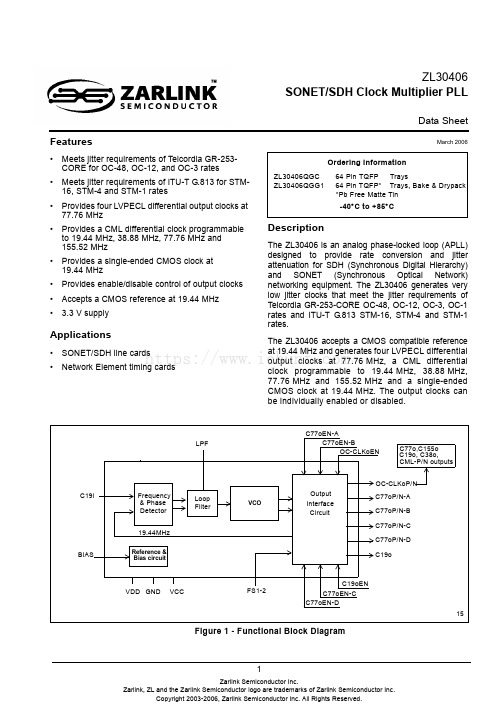
1Features•Meets jitter requirements of Telcordia GR-253-CORE for OC-48, OC-12, and OC-3 rates •Meets jitter requirements of ITU-T G.813 for STM-16, STM-4 and STM-1 rates•Provides four LVPECL differential output clocks at 77.76MHz•Provides a CML differential clock programmable to 19.44MHz, 38.88MHz, 77.76MHz and 155.52MHz•Provides a single-ended CMOS clock at 19.44MHz•Provides enable/disable control of output clocks •Accepts a CMOS reference at 19.44MHz •3.3V supplyApplications•SONET/SDH line cards •Network Element timing cardsDescriptionThe ZL30406 is an analog phase-locked loop (APLL)designed to provide rate conversion and jitter attenuation for SDH (Synchronous Digital Hierarchy)and SONET (Synchronous Optical Network)networking equipment. The ZL30406 generates very low jitter clocks that meet the jitter requirements of Telcordia GR-253-CORE OC-48, OC-12, OC-3, OC-1rates and ITU-T G.813 STM-16, STM-4 and STM-1rates.The ZL30406 accepts a CMOS compatible reference at 19.44MHz and generates four LVPECL differential output clocks at 77.76MHz, a CML differential clock programmable to 19.44MHz, 38.88MHz,77.76MHz and 155.52MHz and a single-ended CMOS clock at 19.44MHz. The output clocks can be individually enabled or disabled.March 2006Ordering InformationZL30406QGC 64 Pin TQFP TraysZL30406QGG164 Pin TQFP*Trays, Bake & Drypack *Pb Free Matte Tin-40°C to +85°CFigure 1 - Functional Block DiagramFrequency Detector VCOC77oP/N-A Interface CircuitLPFFS1-2C77oP/N-B C77oP/N-C VDD GND VCC C77oP/N-D C19oC19oEN OC-CLKoP/NOC-CLKoENC155o CML-P/N outputsLoop FilterC77oEN-C C19iC77o , C19o, C38o, C77oEN-BBIASC77oEN-AC77oEN-D& Phase Output19.44MHz15Reference &Bias circuitZL30406SONET/SDH Clock Multiplier PLLData Sheethttps:///ZL30406Data SheetFigure 2 - TQFP 64 pin (Top View)Change SummaryThe following table captures the changes from the February 2005 issue.Pin DescriptionPage ItemChange1Updated Ordering Information.Pin Description TablePin #Name Description1GND Ground. 0 volt.2VCC1Positive Analog Power Supply. +3.3V ±10%3VCC Positive Analog Power Supply. +3.3V ±10%45OC-CLKoN OC-CLKoP SONET/SDH Clock (CML Output). These outputs provide a programmable differential CML clock at 19.44MHz, 38.88MHz, 77.76MHz and 155.52MHz. The output frequency is selected with FS2 and FS1 pins.6GND Ground. 0 volt7VCC2Positive Analog Power Supply. +3.3V ±10%505254565860626434363840444648423230282624222018GND VDD GND VCC VDD VDD GNDGND NC GND GND NC GND C19o VCC G N D N C C 19o E N F S 1 F S 2 I C N C V D D C 19i V D D N C N C V D D G N D V C C C 77o P -C C 77o N -C G N D V C C C 77o P -B C 77o N -B G N D V C C C 77o P -A C 77o N -A G N D C 77o P -D C 77o N -D V C C 161412106428GND VCC1VCCOC-CLKoN OC-CLKoPGND VCC2LPF C77oEN-B C77oEN-DGND BIASOC-CLKoEN C77oEN-A C77oEN-C GND G N D G N D G N DGND ZL3040665 - EP_GNDhttps:///ZL30406Data Sheet8LPF Low Pass Filter (Analog). Connect to this pin external RC network (R F and C F ) for the low pass filter.9GND Ground. 0 volt 10GND Ground. 0 volt11BIAS Bias. See Figure 11 for the recommended bias circuit.12OC-CLKoENSONET/SDH Clock Enable (CMOS Input). If tied high this control pin enables the OC-CLKoP/N differential driver. Pulling this input low disables the output clock without deactivating differential drivers.13C77oEN-AC77 Clock Output Enable A (CMOS Input). If tied high this control pinenables the C77oP/N-A output clock. Pulling this input low disables the output clock without deactivating differential drivers.14C77oEN-BC77 Clock Output Enable B (CMOS Input). If tied high this control pinenables the C77oP/N-B output clock. Pulling this input low disables the output clock without deactivating differential drivers.15C77oEN-CC77 Clock Output Enable C (CMOS Input). If tied high this control pinenables the C77oP/N-C output clock. Pulling this input low disables the output clock without deactivating differential drivers.16C77oEN-DC77 Clock Output Enable D (CMOS Input). If tied high this control pinenables the C77oP/N-D output clock. Pulling this input low disables the outputclock without deactivating differential drivers.17GND Ground. 0 volt18VDD Positive Digital Power Supply. +3.3V ±10%19NC No internal bonding Connection. Leave unconnected.20NC No internal bonding Connection. Leave unconnected.21NC No internal bonding Connection. Leave unconnected.22VDD Positive Digital Power Supply. +3.3V ±10%23IC Internal Connection. Connect this pin to Ground (GND).2425FS2FS1Frequency Select 2-1 (CMOS Input). These inputs program the clockfrequency on the OC-CLKo output. The possible output frequencies are 19.44MHz (00), 38.88MHz (01), 77.76MHz (10), 155.52MHz (11).26C19oENC19o Output Enable (CMOS Input). If tied high this control pin enables the C19o output clock. Pulling this pin low forces output driver into a high impedance state.27GND Ground. 0 volt28C19i C19 Reference Input (CMOS Input). This pin is a single-ended input reference source used for synchronization. This pin accepts 19.44MHz. 29VDD Positive Digital Power Supply. +3.3V ±10%30GND Ground. 0 volt31NC No internal bonding Connection. Leave unconnected.32GNDGround. 0 volt.Pin Description Table (continued)Pin #Name Descriptionhttps:///ZL30406Data Sheet33GND Ground. 0 volt34VDD Positive Digital Power Supply. +3.3V ±10%35C19o C19 Clock Output (CMOS Output). This pin provides a single-ended CMOS clock at 19.44MHz.36GND Ground. 0 volt37NC No internal bonding Connection. Leave unconnected.38GND Ground. 0 volt 39GND Ground. 0 volt40NC No internal bonding Connection. Leave unconnected.41GND Ground. 0 volt42VDD Positive Digital Power Supply. +3.3V ±10%43GND Ground. 0 volt44VCC Positive Analog Power Supply. +3.3V ±10%45GND Ground. 0 volt46VDD Positive Digital Power Supply. +3.3V ±10%47VCC Positive Analog Power Supply. +3.3V ±10%48GNDGround. 0 volt49VCC Positive Analog Power Supply. +3.3V ±10%.5051C77oN-D C77oP-D C77 Clock Output (LVPECL Output). These outputs provide a differentialLVPECL clock at 77.76MHz. Unused LVPECL port should be left unterminated to decrease supply current.52GND Ground. 0 volt53VCC Positive Analog Power Supply. +3.3V ±10%.5455C77oP-C C77oN-C C77 Clock Output (LVPECL Output). These outputs provide a differential LVPECL clock at 77.76MHz. Unused LVPECL port should be left unterminated to decrease supply current. 56GND Ground. 0 volt57VCC Positive Analog Power Supply. +3.3V ±10%.5859C77oN-B C77oP-B C77 Clock Output (LVPECL Output). These outputs provide a differential LVPECL clock at 77.76MHz. Unused LVPECL port should be left unterminated to decrease supply current.60GND Ground. 0 volt61VCC Positive Analog Power Supply. +3.3V ±10%.6263C77oP-A C77oN-A C77 Clock Output (LVPECL Output). These outputs provide a differential LVPECL clock at 77.76MHz. Unused LVPECL port should be left unterminated to decrease supply current.64GND Ground. 0 volt65EP_GND Exposed die Pad Ground. 0 volt (connect to GND)Pin Description Table (continued)Pin #Name Descriptionhttps:///ZL30406Data Sheet1.0 Functional DescriptionThe ZL30406 is an analog phased-locked loop which provides rate conversion and jitter attenuation for SONET/SDH OC-48/STM-16, OC-12/STM-4 and OC-3/STM-1 applications. A functional block diagram of the ZL30406 is shown in Figure 1 and a brief description is presented in the following sections.1.1 Frequency/Phase DetectorThe Frequency/Phase Detector compares the frequency/phase of the input reference signal with the feedback signal from the Frequency Divider circuit and provides an error signal corresponding to the frequency/phase difference between the two. This error signal is passed to the Loop Filter circuit and averaged to control the VCO frequency.1.2 Loop FilterThe Loop Filter is a low pass filter. This low pass filter ensures that the network jitter requirements are met for an input reference frequency of 19.44MHz. The corner frequency of the Loop Filter is configurable with an external capacitor and resistor connected to the LPF pin and ground as shown below.Figure 3 - External Loop Filter1.3 VCOThe voltage-controlled oscillator (VCO) receives the filtered error signal from the Loop Filter, and based on the voltage of the error signal, generates a primary frequency. The VCO output is connected to the Output Interface Circuit that divides VCO frequency and buffers generated clocks.R F C FInternal Loop FilterZL30406LPFRF=8.2 k Ω, CF=470 nF (for 14 kHz PLL bandwidth)https:///ZL30406Data Sheet1.4 Output Interface CircuitThe output of the VCO is used by the Output Interface Circuit to provide four LVPECL differential clocks at 77.76MHz, one programmable CML differential clock (19.44MHz, 38.88MHz, 77.76MHz, 155.52MHz) controlled with FS1-2 pins and a single-ended 19.44MHz output clock. This block provides also a 19.44MHz feedback clock that closes PLL loop. Each output clock can be enabled or disabled individually with the associated Output Enable pin.To reduce power consumption and achieve the lowest possible intrinsic jitter the unused output clocks must be disabled. If any of the LVPECL outputs are disabled they must be left open without any terminations.The output clock frequency of the OC-CLKo CML differential output clock is selected with FS1-2 pins as shown in the following table.Output Clocks Output Enable PinsC77oP/N-A C77oEN-A C77oP/N-B C77oEN-B C77oP/N-C C77oEN-C C77oP/N-D C77oEN-D OC-CLKoP/NOC-CLKoEN C19oC19oENTable 1 - Output Enable ControlFS2FS1OC-CLKo Frequency 0019.44 MHz 0138.88 MHz 1077.76 MHz 11155.52 MHzTable 2 - OC-CLKo Clock Frequency Selectionhttps:///ZL30406Data Sheet2.0 Applications2.1 Ultra-Low Jitter SONET/SDH Equipment ClocksThe ZL30406 functionality and performance complements the entire family of the Zarlink’s advanced network synchronization PLLs. Its superior jitter filtering characteristics exceed requirements of SONET/SDH optical interfaces operating at OC-48/STM-16 rate (2.5Gbit/s). The ZL30406 in combination with the MT90401 or the ZL30407 (SONET/SDH Network Element PLLs) provides the core building blocks for high quality equipment clocks suitable for network synchronization (see Figure 4).Figure 4 - SONET/SDH Equipment Timing CardMT90401ZL30406OC-CLKo CML38.88 MHz, 19.44 MHz77.76 MHz19.44 MHzC77oA LVPECLC77oB LVPECLC77oC LVPECLC77oD LVPECLC19o CMOSC19iC19o CMOS C155o LVDS C34o/C44o CMOS C16o CMOS C8o CMOS C6o CMOS 19.44 MHz C2o CMOS C1.5o CMOS F8o CMOS F0o CMOS77.76 MHz77.76 MHz77.76 MHz155.52 MHzC4o CMOS 34.368 MHz or 44.736 MHz 16.384 MHz 8.192 MHz 6.312 MHz 4.096 MHz 2.048 MHz 1.544 MHz 8 kHz 8 kHzPRI SECPRIOR SECOR LOCK HOLDOVERRefSel RefAlign R F LPFC FO C -C L K o E N155.52 MHz, 77.76 MHz C 77o E N -AC 77o E N -BC 77o E N -CC 77o E N -DC 19o E ND S C SR /W A 0 - A 6D 0 - D 7uPData PortController PortSynchronization Reference ClocksNote: Only main functional connections are shown20 MHz C 20iF16o CMOS OCXO8 kHz or ZL30407https:///ZL30406Data SheetThe ZL30406 in combination with the MT9046 provides an optimum solution for SONET/SDH line cards (see Figure 5).Figure 5 - SONET/SDH Line CardMT9046ZL30406OC-CLKo CML 38.88 MHz, 19.44 MHz77.76 MHz 19.44 MHzC77oA LVPECLC77oB LVPECL C77oC LVPECL C77oD LVPECL C19o CMOS C19iC19o CMOS C16o CMOS C8o CMOS C6o CMOS 19.44 MHz C2o CMOS C1.5o CMOS F8o CMOS F0o CMOS77.76 MHz 77.76 MHz 77.76 MHzC4o CMOS 16.384 MHz 8.192 MHz 6.312 MHz 4.096 MHz 2.048 MHz 1.544 MHz 8 kHz 8 kHzPRI SECLOCK HOLDOVERRSELR 1LPFC 1O C -C L K o E N155.52 MHz, 77.76 MHzC 77o E N -AC 77o E N -BC 77o E N -CC 77o E N -DC 19o E NM S 1F S 2F L O C K uCSynchronization Reference ClocksNote: Only main functional connections are shown20 MHz F16o CMOS TCXO8 kHz C 2R 1 = 680 ΩC 1 = 820 nF C 2 = 22 nFC20iM S 2F S 1P C C i Hardware ControlT C L Rhttps:///ZL30406Data Sheet2.2 Recommended Interface Circuit 2.2.1 LVPECL to LVPECL InterfaceThe C77oP/N-A, C77oP/N-B, C77oP/N-B, and C77oP/N-D outputs provide differential LVPECL clocks at 77.76MHz. The LVPECL output drivers require a 50Ω termination connected to the VCC-2V source for each output terminal at the terminating end as shown below. The terminating resistors should be placed as close as possible to the LVPECL receiver.Figure 6 - LVPECL to LVPECL Interface2.2.2 CML to CML InterfaceThe CMLP/N output provides a differential CML/LVDS compatible clock at 19.44MHz, 38.88MHz, 77.76MHz,155.52MHz selected with FS1-2 pins. The output drivers require a 50Ω load at the terminating end if the receiver is CML type.Figure 7 - CML to CML InterfaceLVPECL LVPECL ZL30406Z=50 ΩZ=50 ΩC77oP-AC77oN-AReceiverGNDTypical resistor values: R1 = 130Ω, R2 =82ΩR1R2VCC=+3.3 VR1R2VCC0.1 uF+3.3 VDriverZL30406CML Z=50 ΩCML50 ΩOC-CLKoPOC-CLKoNDriverGNDVCCReceiver0.1 uF+3.3 V50 ΩZ=50 Ω0.1 uF0.1 uFLow Impedance DC bias sourcehttps:///ZL30406Data Sheet2.2.3 CML to LVDS InterfaceTo configure the driver as an LVDS driver, external biasing resistors are required to set up the common mode voltage as specified by ANSI/TIA/EIA-644 LVDS standard. The standard specifies the V CM (common mode voltage)as minimum 1.125V, typical 1.2V, and maximum 1.375V. The following figure provides a recommendation for LVDS applications.Figure 8 - LVDS Termination2.2.4 CML to LVPECL InterfaceIn the case when more than four 77.76 MHz clocks are required to drive LVPECL receivers then the unused OC-CLKo clock (CML output) can be configured to output the 77.76 MHz clock and interface to the LVPECL receiver asis shown in the Figure 9. The terminating resistors should be placed as close as possible to the LVPECL receiver.Figure 9 - CML to LVPECL InterfaceZL30406CML Z=50 ΩZ=50 ΩDriver0.1 uF+3.3 VGNDVCCLVDS 10 nF10 nFReceiverR1R2VCC=+3.3 VR1R2100ΩTypical resistor values: R1 = 16 k Ω, R2 = 10 k ΩOC-CLKoPOC-CLKoNLVPECL CML ZL30406Z=50 ΩZ=50 ΩReceiverGNDTypical resistor values: R1 = 82 Ω, R2 =130 ΩR1R2VCC=+3.3 VR1R2VCC0.1 uF+3.3 VDriver10 nF10 nFOC-CLKoPOC-CLKoN77.76MHz https:///ZL30406Data Sheet2.3 Tristating LVPECL OutputsThe ZL30406 has four differential 77.76MHz LVPECL outputs, which can be used to drive four different OC-3/OC-12/OC-48 devices such as framers, mappers and SERDES. In the case where fewer than four clocks are required,a user can disable unused LVPECL outputs on the ZL30406 by pulling the corresponding enable pins low. When disabled, voltage at the both pins of the differential LVPECL output will be pulled up to Vcc - 0.7V.For applications requiring the LVPECL outputs to be in a tri-state mode, external AC coupling capacitors can be used as shown in Figure 10. Typically this might be required in hot swappable applications.Resistors R1 and R2 are required for DC bias of the LVPECL driver. Capacitors C1 and C2 are used as AC coupling capacitors. During disable mode (C77oEN pin pulled low) those capacitors present infinite impedance to the DC signal and to the receiving device this looks like a tristated (High-Z) output. Resistors R3, R4, R5 and R6are used to terminate the transmission line with 50 ohm impedance and to generate DC bias voltage for the LVPECL receiver. If the LVPECL receiver has an integrated 50 ohm termination and bias source, resistors R3, R4,R5 and R6 should not be populated.Figure 10 - Tristatable LVPECL OutputsZ=50Z=50C77oENZL304060.1 uC10.1 uC2R482.5R682.5R5127R3127R1200R22003.3 V 3.3 V https:///ZL30406Data Sheet 2.4 Power Supply and BIAS Circuit Filtering RecommendationsFigure 11 presents a complete filtering arrangement that is recommended for applications requiring maximum jitter performance. The level of required filtering is subject to further optimization and simplification. Please check Zarlink’s web site for updates.Figure 11 - Power Supply and BIAS circuit filteringZL30406Data Sheet3.0 Characteristics†Voltages are with respect to ground unless otherwise stated.‡Exceeding these values may cause permanent damage. Functional operation under these conditions is not implied.†Voltages are with respect to ground unless otherwise stated.‡Typical figures are for design aid only: not guaranteed and not subject to production testing.‡Absolute Maximum Ratings †CharacteristicsSym Min.‡Max.‡Units 1Supply voltage V DDR , V CCRTBD TBD V 2Voltage on any pin V PIN -0.5V CC + 0.5V DD + 0.5V 3Current on any pin I PIN -0.530mA 4ESD Rating V ESD 1500V 5Storage temperature T ST -55125°C 6Package power dissipationP PD1.8WRecommended Operating Conditions †CharacteristicsSym.Min.Typ.‡Max.Units Notes1Operating Temperature T OP -4025+85°C 2Positive SupplyV DD , V CC V CC_VCO3.03.33.6VDC Electrical Characteristics †CharacteristicsSym.Min.Typ.‡Max.Units Notes 1Supply CurrentI DD +I CC140155mALVPECL, CMLdrivers disabled and unterminated 2Incremental Supply Current to single LVPECL driver (driver enabled and terminated, see Figure 6)I LVPECL40mANote 1,23Incremental Supply Current to CML driver (driver enabled and terminated, see Figure 7)I CML24mA Note 34CMOS: High-level input voltageV IH 0.7V DDV DD V 5CMOS: Low-level input voltageV IL 00.3V DDV 6CMOS: Input leakage current, C19iI IL1uAV I = V DD or 0Vhttps:///ZL30406Data Sheet†: Voltages are with respect to ground unless otherwise stated.‡:Typical figures are for design aid only: not guaranteed and not subject to production testing.Note:Supply voltage and operating temperature are as per Recommended Operating ConditionsNote 1:The I LVPECL current is determined by termination network connected to LVPECL outputs. More than 25% of this current flowsoutside the chip and it does not contribute to the internal power dissipation. Note 2:LVPECL outputs terminated with Z T = 50Ω resistors biased to V CC -2V (see Figure 6)Note 3:CML outputs terminated with Z T = 50Ω resistors connected to low impedance DC bias voltage source (see Figure 7)7CMOS: Input bias current for pulled-down inputs: FS1, FS2, C77oEN-A, C77oEN-C, C77oEN-D, OC-CLKoEN I B-PU300uAV I = V DD8CMOS: Input bias current for pulled-up inputs: , C77oEN-B, C19o_ENI B-PD90uAV I = 0V9CMOS: High-level output voltageV OH 2.4V I OH = 8 mA 10CMOS: Low-level output voltageV OL 0.4V I OL = 4 mA 11CMOS: C19o output rise time (18pF)T R 1.8 3.3ns 18 pF load 12CMOS: C19o output fall time (18pF)T F1.1 1.4ns 18 pF load 13LVPECL: Differential output voltageIV OD_LVPECL I 1.30V Note 214LVPECL: Offset voltageV OS_LVPECLVcc-1.38Vcc-1.27Vcc-1.15V Note 215LVPECL: Output rise/fall times T RF 260ps Note 216CML: Differential output voltageIV OD_CML I 0.70V Note 317CML: Offset voltage (Also referred to as common mode voltage)V OS_CMLVcc-0.58Vcc-0.54Vcc-0.50VNote 318CML: Output rise/fall timesT RF120ps Note 3DC Electrical Characteristics † (continued)CharacteristicsSym.Min.Typ.‡Max.Units Notes https:///ZL30406Data SheetFigure 12 - Output Timing Parameter Measurement Voltage Levels† Supply voltage and operating temperature are as per Recommended Operating Conditions.‡Typical figures are for design aid only: not guaranteed and not subject to production testing.Figure 13 - C19i Input to C19o and C77o Output TimingAC Electrical Characteristics †- Output Timing Parameters Measurement Voltage LevelsCharacteristicsSym CMOS ‡LVPECL CMLUnits 1Threshold VoltageV T-CMOS V T-LVPECL V T-CML0.5V DD0.5V OD_LVPECL0.5V OD_CMLV2Rise and Fall Threshold Voltage High V HM 0.7V DD 0.8V OD_LVPECL 0.8V OD_CML V 3Rise and Fall Threshold Voltage LowV LM0.3V DD0.2V OD_LVPECL0.2V OD_CMLVAC Electrical Characteristics †- C19i Input to C19o and C77o Output TimingCharacteristicsSym.Min.Typ.‡Max.Units Notes1C19i to C19o delay t C19D 6.7ns 2C19i to C77oA delayt C77D-4nsV T All SignalsV HM V LMt IF , t OFt IR , t ORTiming Reference Pointshttps:///ZL30406Data Sheet AC Electrical Characteristics† - C19i Input to OC-CLKo Output Delay Timing (CML)Characteristics Sym.Min.Typ.‡Max.Units Notes1C19i to OC-CLKo(19) delay t OC-CLK19D 3.2ns2C19i to OC-CLKo(38) delay t OC-CLK38D 3.0ns3C19i to OC-CLKo(77) delay t OC-CLK77D 2.7ns4C19i to OC-CLKo(155) delay t OC-CLK155D 2.4ns† Supply voltage and operating temperature are as per Recommended Operating Conditions.‡Typical figures are for design aid only: not guaranteed and not subject to production testing.Figure 14 - C19i Input to OC-CLKo Output TimingZL30406Data SheetAC Electrical Characteristics†- C77 Clocks Output TimingCharacteristics Sym.Min.Typ.‡Max.Units Notes 1C77oA to C77oB t C77D-AB100ps2C77oA to C77oC t C77D-AC100ps3C77oA to C77oD t C77D-AD100ps† Supply voltage and operating temperature are as per Recommended Operating Conditions.‡Typical figures are for design aid only: not guaranteed and not subject to production testing.Figure 15 - C77oB, C77oC, C77oD Outputs TimingZL30406Data SheetPerformance Characteristics - Functional- (V CC = 3.3V ±10%; T A = -40 to 85°C )†Typical figures are for design aid only: not guaranteed and not subject to production testing.‡Loop Filter components: R F =8.2 k Ω, C F =470 nF†Typical figures are for design aid only: not guaranteed and not subject to production testing.‡Loop Filter components: R F =8.2 k Ω, C F =470 nFCharacteristicsMin.Max.Units Notes1Pull-in range ±1000ppm 2Lock Time300msPerformance Characteristics: Output Jitter Generation - GR-253-CORE conformance - (V CC = 3.3V ±10%; T A = -40 to 85°C)GR-253-CORE Jitter Generation Requirements ZL30406 Jitter Generation Performance Interface (CategoryII)JitterMeasurementFilter Limit in UI Equivalent limit in time domainTyp.†Max.‡Units 1OC-48STS-4812kHz - 20MHz0.1 UIpp 40.2-16.9ps P-P 0.01UI RMS 4.02 1.3 2.1ps RMS 2OC-12STS-1212kHz - 5MHz0.1 UIpp161-9.0ps P-P 0.01UI RMS16.10.71.3ps RMSPerformance Characteristics: Output Jitter Generation - ETSI EN 300 462-7-1 conformance - (V CC = 3.3V ±10%;T A = -40 to 85°C)EN 300 462-7-1 Jitter Generation RequirementsZL30406 Jitter Generation Performance Interface JitterMeasurementFilter Limit in UI Equivalent limit in time domainTyp.†Max.‡Units 1STM-161MHz to 20MHz0.1 UIpp40.2-12.6ps P-P -- 1.0 1.5ps RMS 5kHz to 20MHz0.5UIpp201-17.1ps P-P -- 1.3 2.2ps RMS 2STM-4250kHz to 5MHz0.1 UIpp161- 5.8ps P-P --0.460.9ps RMS 1kHz to 5MHz0.5 UIpp804-29.8ps P-P -- 2.43.2ps RMShttps:///ZL30406Data Sheet†Typical figures are for design aid only: not guaranteed and not subject to production testing.‡Loop Filter components: R F =8.2 k Ω, C F =470 nFPerformance Characteristics: Output Jitter Generation - G.813 conformance (Option 1 and 2) - (V CC = 3.3V±10%; T A = -40 to 85°C)G.813 Jitter Generation RequirementsZL30406 Jitter Generation PerformanceInterfaceJitterMeasurementFilter Limit in UIEquivalent limit in time domainTyp.†Max.‡UnitsOption 11STM-161MHz to 20MHz0.1 UIpp40.2-12.6ps P-P -- 1.0 1.5ps RMS 5kHz to 20MHz0.5 UIpp201-17.1ps P-P -- 1.3 2.2ps RMS 2STM-4250kHz to 5MHz0.1 UIpp161- 5.8ps P-P --0.460.9ps RMS 1kHz to 5MHz0.5 UIpp804-29.8ps P-P --2.43.2ps RMS Option 23STM-1612kHz - 20MHz0.1 UIpp 40.2-16.9ps P-P -- 1.32.1ps RMS 4STM-412kHz - 5MHz0.1 UIpp161-9.0ps P-P --0.71.3ps RMShttps:///。
HT00-03083中文资料

Height 6.35 6.35 6.35 10.20 6.00 6.35 7.37 6.60 9.80 6.22 5.50 6.22 6.22 6.22 5.50 5.50 5.50 6.06 6.06 6.06 6.22 6.22 6.22 7.34 7.34 7.34 6.95 5.77 6.95 5.77 6.95 6.95 5.77 5.77 5.77 5.77 5.77 6.95
元器件交易网
Electrical / Environmental
T1/CEPT/ISDN-Pri Telecom Products
S RoH nt for
lia Comp dels o ‘LF’ M
• • • • •
Meets the required 1500 Vrms line isolation Standard Operating Temperature Range 0°C to +70°C Extended Operating Temperature Range -40°C to +85°C RoHS Peak Solder Rating 260°C Non-RoHS Peak Solder Rating 235°C
Style 6-pin DIL 6-pin DIL 6-pin DIL 10-pin DIL 12-pin SMT 14-pin DIL 14-pin DIL 14-pin DIL 16-pin DIL 16-pin SMT 16-pin SMT 16-pin SMT 16-pin SMT 16-pin SMT 16-pin SMT 16-pin SMT 16-pin SMT 16-pin SMT 16-pin SMT 16-pin SMT 16-pin SMT 16-pin SMT 16-pin SMT 32-pin SMT 32-pin SMT 32-pin SMT 40-pin SMT 40-pin SMT 40-pin SMT 40-pin SMT 40-pin SMT 40-pin SMT 40-pin SMT 40-pin SMT 40-pin SMT 40-pinSMT 40-pin SMT 40-pin SMT
SP20_Manual_cn说明书

+SP20B/SP20F/SP20X/SP20P编程器使用手册2022-12-20 Revision A6深圳硕飞科技有限公司SHENZHEN SFLY TECHNOLOGY CO.,LTD.目录第一章简介1.1 性能特点 -------------------------------------------------------------------------------------------- 31.2 SP20系列编程器参数表----------------------------------------------------------------------------- 4第二章编程器硬件2.1 编程器主机------------------------------------------------------------------------------------------ 52.2 附件------------------------------------------------------------------------------------------------- 5第三章快速使用3.1 软件安装 -------------------------------------------------------------------------------------------- 63.2 烧录芯片步骤 --------------------------------------------------------------------------------------- 63.3 读取芯片数据并写入新的芯片----------------------------------------------------------------------- 83.4 联机模式指示灯状态 -------------------------------------------------------------------------------- 9第四章脱机烧录4.1下载脱机数据 ---------------------------------------------------------------------------------------104.2 脱机烧录操作----------------------------------------------------------------------------------------11手动方式 -------------------------------------------------------------------------------------------11 自动控制方式(通过ATE接口控制)---------------------------------------------------------------124.3 脱机模式指示灯状态 -------------------------------------------------------------------------------12第五章ISP模式烧录5.1选择ISP烧录模式 ----------------------------------------------------------------------------------135.2 ISP接口定义----------------------------------------------------------------------------------------135.3 连接目标芯片 --------------------------------------------------------------------------------------145.4 选择ISP供电方式----------------------------------------------------------------------------------145.5 烧录操作 -------------------------------------------------------------------------------------------14第六章多机模式烧录6.1 编程器硬件连接 ------------------------------------------------------------------------------------156.2 烧录操作 -------------------------------------------------------------------------------------------16附录一常见问题解答 -------------------------------------------------------------------------------------------- 17附录二免责声明------------------------------------------------------------------------------------------------- 18附录三修订记录-------------------------------------------------------------------------------------------------19第一章简介SP20系列(SP20B/SP20F/SP20X/SP20P)编程器是深圳硕飞科技最新推出的一款SPI FLASH专用高速量产型编程器,是SP16系列的升级版,全面支持国内外各厂商的SPI NOR FLASH、I2C/MicroWire 等EEPROM的高速量产烧录。
FBR12HD03-P-CSA中文资料
(a)Series Name FBR12: FBR12 Series(b)Enclosure & Coil PowerN: Standard (plastic sealed type)W : High dielectric strength type (plastic sealed type)H: High sensitivity type(c)Coil Type D : DC coil(d)Nominal VoltageRefer to the COIL DATA CHART(e)Contact MaterialNil : Gold-overlay silver-nickel –P : Gold-overlay silver-palladium(f)Custom Designation To be assigned custom specification(g)CSA Standard–CSA : UL114 + CSA recognized–CSA : UL1950 + CSA (under application)Note:The designation name is stamped on the top of the relay case as follows:(Example) Designation ordered: FBR12ND05Stamp:12ND05s FEATURESq Super miniature size: 0.2 inch × 0.1 inch grid, 12 pin DIP Up to 50% less volume and board area than previous generation telecom relay.q Slim type for high density mountingqConforms to Bellcore TR-NWT-001089 and FCC Part 68 requirementsq UL recognized and CSA certified q Low power consumptionqConforms to IEC 950 (W type only)– 2.5 mm clearance and creepage between coil and contacts –5000 V surge strength between coil and contacts (2x10µs surge wave)–2000 Vrms dielectric strength between coil and contacts –UL 1950 and IEC950 (approval in process)FBR12N D 12 –P –**(–CSA)[Example](a)(b)(c)(d)(e)(f )(g)s ORDERING INFORMATIONs SAFETY STANDARD AND FILE NUMBERSNominal coil voltageContact rating0.5 A 125 VDC resistive 3 to 24 VDC2 A 30 VDC resistive 0.3 A 110 VAC resistiveUL508, 1950, 114 (File No. E63615)C22.2 No. 0, No. 14 (File No. LR40304 or LR64026)N OT F O R N E W D E S I G N F B R 12 S E R I E ST O B E D I S C O N T I N I E DN OT F O R N E W D E S I G N F B R 12 S E R I E ST O B E D I S C O N T I N I E DLifeMechanical1 × 108 operations minimumElectrical DC2 × 105 operations minimum 5 × 10⁵ operations minimum (at contact rating)AC1 × 105 operations minimum200 × 103 operations minimumOtherVibration Misoperation 10 to 55 Hz (double amplitude of 3.3 mm)ResistanceEndurance 10 to 55 Hz (double amplitude of 5.0 mm)Shock Misoperation 500 m/s 2 (11±1 ms)ResistanceEndurance 1,000 m/s 2 ( 6 ±1 ms)WeightApprox. 1.5 g Approx. 1.9 g Approx. 1.5 g Approx. 1.9 gs SPECIFICATIONSItemStandard (Gold-overlay silver-nickel)-P type (Gold-overlay silver-palladium)StandardHigh dielectric StandardHigh dielectric strength typestrength typeContactArrangement 2 form C (DPDT)Material Gold-overlay silver-nickel Gold-overlay silver-palladiumStyleBifurcatedResistance (initial)Maximum 100 m Ω (at 0.1 A 6 VDC)Rating (resistive)0.5 A 125 VAC or 1 A 30 VDCMaximum Carrying Current 2 A (at 20°C)Maximum Switching Power 62.5 VA or 60 W Max. Switching Voltage*1250 VAC or 220 VDCMaximum Switching Current 2 AMinimum Switching Load*210 µA 10 VDC (reference)Capacitance Approximately 1.0 pF (between open contacts, adjacent contacts )(at 10 kHz) Approximately1.0 pF (between coil and contacts)CoilNominal power (at 20°C)Approximately Approximately Approximately Approximately 0.14 to 0.2 W 0.23 to 0.25 W 0.14 to 0.2 W 0.23 to 0.25 WOperate power (at 20°C)Approximately Approximately Approximately Approximately 0.08 to 0.112 W 0.13 to 0.14 W 0.08 to 0.112 W 0.13 to 0.14 WThermal Resistance at Approximately 115°C/WContinuous Thermal Load Operating Temperature –40°C to +85°C (no frost) (refer to the CHARACTERISTIC DATA)Operating Humidity45 to 85%RHTime ValueOperate (at nominal voltage)Maximum 4 msec.Release (at nominal voltage)Maximum 4 msec.Max. Switching Frequency Mechanical 3 Hz or electrical 0.5 Hz (at contact rating)InsulationResistance (initial)Minimum 1000 M Ω (at 500 VDC)Dielectric between open contacts 1,000 VACStrengthadjacent contacts 1 minimumbetween coil and contacts 1,500 VAC 1 min. 2,000 VAC 1 min. 1,500 VAC 1 min. 2,000 VAC 1 min.Surge between open 1,500 VStrength contacts,10 × 700 µsadjacent contactsbetween coil and contacts 2,500 V 5,000 V 2,500 V 5,000 V 2 × 10 µs 2 × 10 µs 2 × 10 µs 2 × 10 µs1,500750107002,5001,250210*1 If the switching voltage exceeds the rated contact voltage, reduce the current. The current values vary according to thetype of load.*2 Values when switching a resistive load at normal room temperature and humidity and in a clean environment.N OT F O R N E W D E S I G N F B R 12 S E R I E ST O B E D I S C O N T I N I E DItemHigh Sensitive TypeStandard (Gold-overlay silver-nickel) -P type (Gold-overlay silver-palladium)ContactArrangement 2 form C (DPDT)MaterialGold-overlay silver-nickel Gold-overlay silver-palladiumStyleBifurcatedResistance (initial)Maximum 100 m Ω (at 0.1 A 6 VDC)Rating (resistive)0.3 A 125 VAC or 1 A 30 VDC Maximum Carrying Current 2 A (at 20°C)Maximum Switching Power 62.5 VA or 30 W Max. Switching Voltage*1250 VAC or 220 VDC Maximum Switching Current 2 AMinimum Switching Load*210m VDC - 10µ ACapacitance Approximately 1.0 pF (between open contacts, adjacent contacts )(at 10 kHz) Approximately1.0 pF (between coil and contacts)CoilNominal power (at 20°C)Approximately 50mWOperate power (at 20°C)Approximately 40m WOperating Temperature –40°C to +70°C (no frost) (refer to the CHARACTERISTIC DATA)Operating Humidity45 to 85%RHTime Value Operate (at nominal voltage)Maximum 5 msec.Release (at nominal voltage)Maximum 5 msec.InsulationResistance (initial)Minimum 1000 M Ω (at 500 VDC)Dielectric between open contacts 750 VAC Strengthadjacent contacts 1 minutebetween coil and contacts 1,500 VAC 1 minutes Surge between open 1,500 V Strength contacts,10 × 700 µsadjacent contactsbetween coil and contacts 2,500 V 2 × 10 µsLifeMechanical1 x 108 operations minimumElectrical DC 2 × 10⁵ operations minimum 5 × 10⁵ operations minimum (at contact rating)AC1 × 105 operations minimum200 × 103 operations minimumOtherVibration Misoperation 10 to 55 Hz (double amplitude of 3.3` mm)ResistanceEndurance 10 to 55 Hz (double amplitude of 5.0 mm)Shock Misoperation 500 m/s 2 (11±1 ms)ResistanceEndurance 1,000 m/s 2 ( 6 ±1 ms)WeightApprox. 1.9 gs SPECIFICATIONS*1 If the switching voltage exceeds the rated contact voltage, reduce the current. The current values vary according to thetype of load.*2 Values when switching a resistive load at normal room temperature and humidity and in a clean environment. The minimum switching load varies with the switching frequency and operation environment.N OT F O R N E W D E S I G N F B R 12 S E R I E ST O B E D I S C O N T I N I E DMODELNominalNominal Coil current Must Must Nominal Operate Coil resistance (at nominal operate operate temperature voltage(±10%)voltage)voltage*1voltage*1powerpowerriseStandard -P type approx.FBR12ND03FBR12ND03-P 3 VDC 64.3 Ω46 mA FBR12ND04FBR12ND04-P 4.5 VDC 145 Ω31 mA FBR12ND05FBR12ND05-P 5 VDC 178 Ω28 mA 75% max.10% min.Approx.Approx.Approx.of nominal of nominal 0.14 W 0.08 W 20 deg FBR12ND06FBR12ND06-P 6 VDC 257 Ω23 mA (at nominalMax.voltage voltage voltage)Max.(at nominal FBR12ND09FBR12ND09-P 9 VDC 579 Ω15 mA voltage)FBR12ND12FBR12ND12-P 12 VDC 1,028 Ω11 mAFBR12ND24FBR12ND24-P24 VDC2,880 Ω8 mA0.2 W0.112 W30 degs COIL DATA CHART*1: Specified values are subject to pulse wave voltage.Note:All values in the table are measured at 20°C.MODELNominalNominal Coil current Must Must Nominal Operate Coil resistance (at nominaloperate release temperature voltage(±10%)voltage)voltage*1voltage*1powerpowerriseStandard-P typeapprox.FBR12WD03FBR12WD03-P 3 VDC 39 Ω77 mA FBR12WD04FBR12WD04-P 4.5 VDC 88 Ω51 mA FBR12WD05FBR12WD05-P 5 VDC 108 Ω46 mA 75% max.10% min.Approx.Approx.Approx.of nominal of nominal 0.23 W 0.13 W 30 deg FBR12WD06FBR12WD06-P 6 VDC 156 Ω38 mA (at nominal(at nominal voltage voltage voltage)Max.voltage)FBR12WD09FBR12WD09-P 9 VDC 352 Ω25 mA FBR12WD12FBR12WD12-P 12 VDC 626 Ω19 mA FBR12WD24FBR12WD24-P 24 VDC2,304 Ω10 mA0.25 W0.14 W33 deg*1: Specified values are subject to pulse wave voltage.Note:All values in the table are measured at 20°C.1.STANDARD2.HIGH DIELECTRIC STRENGTHMODELNominal CoilMust Must Nominal Operate Coil resistance operate release temperature voltage (±10%)voltage*1voltage*1powerpowerriseStandard-P typeFBR12HD03FBR12HD03-P 3 VDC 180 ΩFBR12HD04FBR12HD04-P 4.5 VDC 405 ΩFBR12HD05FBR12HD05-P 5 VDC 500 Ω 80% max.10% min.Approx.Approx.Approx.of nominal of nominal 0.05 W 0.04 W 4 deg FBR12HD06FBR12HD06-P 6 VDC 720 Ω(at nominal(at nominal voltage voltage voltage)Max.voltage)FBR12HD09FBR12HD09-P 9 VDC 1,620 ΩFBR12HD12FBR12HD12-P 12 VDC 2,880 Ω*1: Specified values are subject to pulse wave voltage.Note:All values in the table are measured at 20°C.3. HIGH SENSITIVITY TYPERN EWNE SNNs DIMENSIONSUnit: mm s REFERENCE DATAs CHARACTERISTIC DATALife curve500Contact load current (A)505101100(×104Servicelife(operations)0.5 1.0 1.5 2.0Maximum switching capacityContact load voltage (V)Range of operation temperature and voltageOperating temperature (˚C)Contactloadcurrent(A)Nominalvoltagemultiplyingfactor(%)q Dimensions q Schematics(BOTTOM VIEW)q PC board mounting hole layout30 pcs/Tube±2Distribution of operate and release voltageRated coil voltage multiplying factor (%)60504020301001020304050607080Distribution(%)Distribution of operate and release timeTime (ms)10080602040012345678Contact resistance (mΩ)Distribution of contact resistance8060402001020304050607080Distribution(%)Distribution(%)N OT F O R N E W D E S I G N F B R 12 S E R I E ST O B E D I S C O N T I N I E D© 2004 Fujitsu Components America, Inc. All company and product names are trademarks or registered trademarks of their respective owners. Rev. 07/26/2004.JapanFujitsu Component Limited Gotanda-Chuo Building3-5, Higashigotanda 2-chome, Shinagawa-ku Tokyo 141, Japan Tel: (81-3) 5449-7010Fax: (81-3) 5449-2626Email: promothq@ Web: North and South AmericaFujitsu Components America, Inc.250 E. Caribbean DriveSunnyvale, CA 94089 U.S.A.Tel: (1-408) 745-4900Fax: (1-408) 745-4970Email: marcom@ Web: EuropeFujitsu Components Europe B.V.Diamantlaan 252132 WV Hoofddorp NetherlandsTel: (31-23) 5560910Fax: (31-23) 5560950Email: info.marketing@ Web: Asia PacificFujitsu Components Asia Ltd.102E Pasir Panjang Road#04-01 Citilink Warehouse Complex Singapore 118529Tel: (65) 375-8560Fax: (65) 273-3021Email: fcal@ Fujitsu Components International Headquarter Offices。
ADS830中文资料

Referred to Full Scale
Referred to Full Scale
NTSC, PAL NTSC, PAL Input Tied to Common-Mode
DIGITAL INPUTS
Logic Family Convert Command High Level Input Current(5) (VIN = 5V) Low Level Input Current (VIN = 0V) High Level Input Voltage
ADS830E
PARAMETER
DIFFERENTIAL ANALOG INPUT q PROGRAMMABLE INPUT RANGE:
1Vp-p /2Vp-p q LOW POWER: 170mW q LOW DNL: 0.2LSB q SINGLE +5V SUPPLY OPERATION q 20-PIN SSOP PACKAGE
100 10 +2.4 +1.0 5
CMOS/TTL Compatible Straight Offset Binary
+0.1 +0.2 +4.9 +4.8 +0.1 +2.8 5
–2.5 –2.5
REFB + 0.8 1.25
±0.25 ±53 ±0.3 ±75 58 ±10 ±10 3.0
2.0
2Vp-p 1Vp-p 2Vp-p
–3dBFS
CONVERSION CHARACTERISTICS Sample Rate Data Latency
DYNAMIC CHARACTERISTICS Differential Linearity Error (Largest Code Error)
8205a中文资料
8205a中文资料锂电池保护板根据使用的不同IC和电压具有不同的电路和参数。
常用的保护IC是8261,DW01 +,CS213,GEM5018等。
其中,精工的8261系列具有更好的精度,当然价格也更昂贵。
后者全部在台湾制造。
国内二级市场主要使用DW01 +和CS213。
以下是带有MOS管8205A(8pin)的DW01 +的说明:锂电池保护板的正常工作流程为:当电池电压在2.5V至4.3V之间时,DW01的第一引脚和第三引脚均输出高电平(等于电源电压),第二引脚电压为0V。
此时,DW01的引脚1和3的电压将分别施加到8205A的引脚5和4。
由于8205A中的两个电子开关的G 极连接到DW01的电压,因此它们处于导通状态。
两个电子开关均处于打开状态。
此时,电池单体的负极直接连接至保护板的P-端子,并且保护板具有电压输出。
2.保护板过放电保护控制原理:当电池通过外部负载放电时,电池电压将缓慢降低,与此同时,DW01将通过R1电阻实时监控电池电压。
当电池电压降至约2.3V时,DW01将认为电池电压处于过放电电压状态,引脚1的输出电压立即断开,从而引脚1的电压变为0V,并且开关由于引脚5上没有电压,因此8205A中的电子管关闭。
此时,电池单元的B-和保护板的P-处于断开状态。
即,电池单元的放电电路被切断,并且电池单元将停止放电。
保护板处于过放电状态,并且已经维护。
保护板的P 和P-具有间接充电电压后,DW01通过B-检测到充电电压后,将立即停止过放电状态,并再次在引脚1上输出高电压以开启过放电控制8205A中的电子管。
也就是说,电池单元的B-和保护板的P-被重新连接,并且电池由充电器直接充电。
3.保护板过充保护控制原理:当电池由充电器正常充电时,随着充电时间的增加,电池的电压将越来越高。
当电池电压升至4.4V时,DW01将认为电池电压处于过充电电压状态。
然后立即断开引脚3的输出电压,以使引脚3的电压变为0V,并且由于引脚4上没有电压,因此8205A中的开关管被闭合。
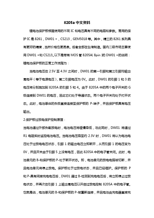
2SK3078A中文资料
TOSHIBA Field Effect Transistor Silicon N Channel MOS Type2SK3078AVHF/UHF Band Amplifier Applications· Output power: P o ≥ 28.0dBmW · Gain: G p ≥ 8.0dB· Drain Efficiency: ηD ≥ 50%Maximum Ratings (Ta = 25°C)Characteristics Symbol Rating UnitDrain-source voltage V DSS10 VGate-source voltage V GSS 5 V Drain current I D 0.5 A Power dissipation P D (Note 1)3WChannel temperature T ch 150 °C Storage temperature rangeT stg−45~150 °CNote 1: Tc = 25°CMarkingElectrical Characteristics (Ta = 25°C)Characteristics Symbol Test Condition Min Typ. Max UnitOutput power P O 28.0 ¾ ¾ dBmW Drain efficiency ηD 50 ¾ ¾ % Power gain G p V DS = 4.5 V, Iidle = 50 mA(V GS = adjust)f = 470 MHz, P i = 20dBmWZ G = Z L == 50 Ω 8.0 ¾ ¾ dB Threshold voltage V th V DS = 4.8 V, I D = 0.5 mA 0.20 ¾ 1.20VDrain cut-off current I DSS V DS = 10 V, V GS = 0 V ¾ ¾ 10 µA Gate-source leakage currentI GSSV GS = 5 V, V DS = 0 V¾¾ 5 µALoad mismatch (Note 2)¾V DS = 6.5 V, f = 470 MHz, P i = 20dBmW,P o = 28.0dBmW (V GS = adjust) VSWR LOAD 10:1 all phaseNo degradation ¾Caution: This transistor is the electrostatic sensitive device. Please handle with caution. Note 2: When the RF output power test fixture is usedUnit: mmJEDEC―JEITA SC-62 TOSHIBA 2-5K1DU WPF Output Power Test FixtureGS DSL1: f 0.6, 5.5ID, 5T L2: f 0.6, 5.5ID, 7TLine: 2 mmP i – P o , G p , EffIidle – G p , EffP i – P oP i – IddVdd – G p , EffP i – P oP i (dBmW)Iidle (mA)P i (dBmW)P i (dBmW)Vdd (V)P i (dBmW)G p (d B m W )P o (d B m W )D r a i n c u r r e n t (m A )P o (d B m W )E f f (%) P o (d B m W )G p (d B )E f f (%)10050Idd (%)255 15 20 10 03020100 302010 082 46Eff3020Vdd Vdd Vdd VddCaution: These are typical curves and devices are not necessarily guaranteed at these curves.P i – IddP i (dBmW)I d d (m A )301020· TOSHIBA is continually working to improve the quality and reliability of its products. Nevertheless, semiconductor devices in general can malfunction or fail due to their inherent electrical sensitivity and vulnerability to physical stress. It is the responsibility of the buyer, when utilizing TOSHIBA products, to comply with the standards of safety in making a safe design for the entire system, and to avoid situations in which a malfunction or failure of such TOSHIBA products could cause loss of human life, bodily injury or damage to property.In developing your designs, please ensure that TOSHIBA products are used within specified operating ranges as set forth in the most recent TOSHIBA products specifications. Also, please keep in mind the precautions and conditions set forth in the “Handling Guide for Semiconductor Devices,” or “TOSHIBA Semiconductor Reliability Handbook” etc.. · The TOSHIBA products listed in this document are intended for usage in general electronics applications (computer, personal equipment, office equipment, measuring equipment, industrial robotics, domestic appliances, etc.). These TOSHIBA products are neither intended nor warranted for usage in equipment that requires extraordinarily high quality and/or reliability or a malfunction or failure of which may cause loss of human life or bodily injury (“Unintended Usage”). Unintended Usage include atomic energy control instruments, airplane or spaceship instruments, transportation instruments, traffic signal instruments, combustion control instruments, medical instruments, all types of safety devices, etc.. Unintended Usage of TOSHIBA products listed in this document shall be made at the customer’s own risk. · The information contained herein is presented only as a guide for the applications of our products. No responsibility is assumed by TOSHIBA CORPORATION for any infringements of intellectual property or other rights of the third parties which may result from its use. No license is granted by implication or otherwise under any intellectual property or other rights of TOSHIBA CORPORATION or others. · The information contained herein is subject to change without notice.000707EAARESTRICTIONS ON PRODUCT USE。
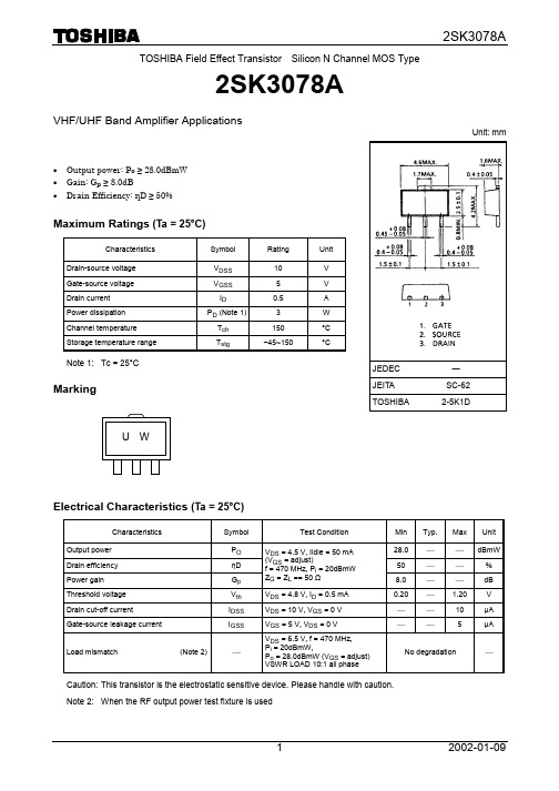
2380中文资料
February 2007© 2006 Fairchild Semiconductor CorporationFSA2380 Rev. 1.0.2FSA2380 — Low R ON (0.75Ω) 3:1 Negative Swing Audio Source SwitchClick here for this datasheet translated into Chinese!FSA2380 — Low R ON (0.75Ω) 3:1 Negative Swing Audio Source SwitchFeatures 10µA Maximum I CCT Current Over An Expanded Control Voltage Range (V IN =2.6V, V CC =4.3V) C ON Capacitance 70pF Typical 0.75Ω Typical On Resistance (R ON )1Bn, 2Bn Ports Support Negative Swing Audio to -2V -3db Bandwidth: > 120 MHzLow Power Consumption (1µA maximum) Power-Off Feature for 1A/2A Pin (I IN < 2µA) Packaged in Pb-Free 14-Pin TSSOP and DQFNApplicationsCell Phone, PDA, Digital Camera, and NotebookLCD Monitor, TV, and Set-Top BoxDescriptionThe FSA2380 is a Double-Pole, Triple Throw (DP3T) multiplexer that routes three dual-channel sources of data or audio under the control of a single pair of select pins. The FSA2380 has special circuitry on the 1A/2A pins to allow a power-off feature. With the V CC supply removed and voltage on the 1A/2A pins, there is minimal leakage current into the 1A/2A data pins. The FSA2380 also features very low quiescent current and a power-off feature to extend battery life. The low quiescent current feature allows mobile handset applications direct interface with the baseband processor general-purpose I/Os. Typical applications involve switching in portables and consumer applications, such as cell phones, digital cameras, and notebooks with hubs or controllers.IMPORTANT NOTE:For additional performance information, please contact analogswitch@ .Ordering InformationPart NumberTop MarkPb-FreePacking DescriptionFSA2380BQX 2380 Yes 14-Terminal Depopulated very thin Quad Flat-pack No leads (DQFN)2.5 x3.0mm, JEDEC MO-241FSA2380MTCX FSA2380 Yes14-Lead Thin Shrink Small Outline Package (TSSOP)4.4mm wide, JEDEC MO-153Analog SymbolControl S0S12B02B22A2B11B01B21A1B1Figure 1.FSA2380 Analog Symbol™TinyBoost© 2006 Fairchild Semiconductor Corporation FSA2380 Rev. 1.0.2 13。
磐启微电子 PAN3020 产品说明书

PAN3020产品说明书低成本高性能Sub-1G无线收发芯片概述PAN3020是一款工作在1GHz以下的多个频段,如315MHz / 433MHz / 868MHz / 915MHz(后称为315频段、433频段、868频段和915频段)等通用ISM频段,的单片无线收发芯片。
该芯片集成射频收发器、频率综合器、晶体振荡器、调制解调器等功能模块,并且支持一对多组网和带ACK的通信模式。
发射输出功率、工作频道以及通信数据率均可配置。
主要特性1.支持1GHz以下的多个频段。
2.支持40Kbps、80Kbps、200Kbps和400Kbps四种通信数据率。
3.最大发射输出功率20dBm;433频段的40Kbps的接收灵敏度-112dBm。
其它特性支持FEC功能 支持连续发射模式SPI 接口速率最高支持8Mbps GFSK通信方式支持最大数据长度为32/64字节 SOP16封装支持16MHz晶振±10ppm 工作电压支持2.2~3.3V数据扰码 数据自动校验自带温度检测功能 支持自动应答及自动重传应用方案遥控器 智能家居工业控制安防系统无线语音MISOMOSICSNSCKIRQCEVSSVDDVDVDDVSS版本 修订时间 更新内容 相关文档V1.5 2016. 06 新增QFN20封装形式 《02_PAN3020硬件设计和调试参考》《03_PAN3020软件设计和调试参考》《04_PAN3020_RFdemo》 《05_PAN3020_SampleCode》 《06_PN3020 各频段软件配置和硬件匹配区别说明》目录1 命名规则 (4)1.1 PAN3020命名规则 (4)1.2 PAN3020系列产品选择 (4)2 电气特性 (4)2.1主要电特性 (4)2.2 极限最大额定值 (4)3 引脚定义 (6)4 工作模式 (8)4.1 工作模式切换 (8)4.2 休眠模式 (9)4.3 待机模式-I (9)4.4 待机模式-II (9)4.5 接收模式 (10)4.6 发射模式 (10)4.7 连续发射模式 (10)5 数据包格式 (11)5.1 DATA FIFO结构 (11)5.2普通模式的数据包形式 (11)5.3 增强模式的数据包形式 (12)5.4 增强模式的ACK包形式 (12)6 通信模式 (13)6.1 普通模式 (14)6.2 增强模式 (14)6.3增强发送模式 (15)6.4 增强接收模式 (17)6.5 增强模式下的数据包识别 (18)6.6 增强模式下的PTX和PRX的时序图 (18)6.7 增强模式下的接收端一对多通信 (19)6.8 中断引脚 (21)7 SPI控制接口 (22)7.1 SPI接口 (22)7.2 SPI 时序 (22)7.3 4线SPI读操作 (23)7.4 4线SPI写操作 (23)7.5 SPI指令格式 (24)8 控制寄存器 (26)9 射频参数设定 (46)9.1 频率设定 (46)9.2 功率设定 (46)9.3 内部时钟输出设定 (46)9.4 晶振的芯片内部电容设定 (46)10 典型应用电路 (48)11 封装尺寸 (50)12 联系方式 (52)1 命名规则1.1 PAN3020命名规则图2 PAN3020系列芯片命名规则1.2 PAN3020系列产品选择表1.1 PAN3020系列产品选择产品型号芯片版本封装形式PAN3020BV B VPAN3020BL B L2 电气特性2.1主要电特性表2.1 主要电特性特 性 条件(除另有规定外,VCC = 3V±5%, TA=25℃)参数值 单位 最小 典型 最大ICC休眠模式 2 uA待机模式I 50 uA待机模式Ⅱ 750 uA 发射模式 (1dBm) 20 mA发射模式 (8dBm) 30 mA发射模式 (15dBm) 50 mA发射模式 (20dBm) 85 mA 接收模式 (DR=400Kbps) 18 18.5 mA接收模式 (DR=200Kbps) 18 18.5 mA 接收模式(DR=80Kbps) 18 18.5 mA 接收模式(DR=40Kbps)1818.5mA系统指标OP f工作频率(315频段) 270 360 MHz 工作频率(433频段) 400 550 MHz 工作频率(868/915频段)800 1100 MHz res PLL锁相环频率步径20 KHz XTAL f晶振频率 16 MHz DR码率40 Kbps 80 Kbps 200 Kbps400 Kbps f调制频偏@40Kbps 20 KHz 调制频偏@80Kbps 40 KHz 调制频偏@200Kbps 100 KHz 调制频偏@400Kbps200 KHz FCH频道间隔@40Kbps 120 KHz 频道间隔@80Kbps 240 KHz 频道间隔@200Kbps 600 KHz 频道间隔@400Kbps1200 KHz 发射模式指标PRF 典型输出功率15 dBm PRFC 输出功率范围(315/433频段) -70 20 dBm 输出功率范围(868/915频段) -70 15 dBm PBW载波调制的20dB 带宽(40Kbps) 80 KHz 载波调制的20dB 带宽(80Kbps) 160 KHz 载波调制的20dB 带宽(200Kbps) 400 KHz 载波调制的20dB 带宽(400Kbps)800 KHz 接收模式指标max RX误码率<0.1%时的最大接收幅度 0 dBm RXSENS接收灵敏度(0.1%BER,DR=40Kbps,△f=±20KHz,@433频段)-112dBm接收灵敏度(0.1%BER,DR=80Kbps,△f=±40KHz,-109 dBm@433频段)-106 dBm 接收灵敏度(0.1%BER,DR=200Kbps,△f=±100KHz,@433频段)-103 dBm 接收灵敏度(0.1%BER,DR=400Kbps,△f=±200KHz,@433频段)-112 dBm 接收灵敏度(0.1%BER,DR=40Kbps,△f=±20KHz,@315频段)-109 dBm 接收灵敏度(0.1%BER,DR=80Kbps,△f=±40KHz,@315频段)-106 dBm 接收灵敏度(0.1%BER,DR=200Kbps,△f=±100KHz,@315频段)-103 dBm 接收灵敏度(0.1%BER,DR=400Kbps,△f=±200KHz,@315频段)接收灵敏度(0.1%BER,-107 dBm DR=40Kbps,△f=±20KHz,@868频段)-104 dBm 接收灵敏度(0.1%BER,DR=80Kbps,△f=±40KHz,@868频段)-101 dBm 接收灵敏度(0.1%BER,DR=200Kbps,△f=±100KHz,@868频段)-98 dBm 接收灵敏度(0.1%BER,DR=400Kbps,△f=±200KHz,@868频段)-107 dBm 接收灵敏度(0.1%BER,DR=40Kbps,△f=±20KHz,@915频段)-104 dBm 接收灵敏度(0.1%BER,DR=80Kbps,△f=±40KHz,@915频段)接收灵敏度(0.1%BER,DR=200Kbps,△f=±100KHz,@915频段) -101 dBm接收灵敏度(0.1%BER,DR=400Kbps,△f=±200KHz,@915频段)-98 dBmCO C I /同频的通道选择性@40Kbps 13 dBc ST C 1/I第1相邻道选择性@40Kbps -21 dBc ND C 2/I 第2相邻道选择性@40Kbps -35 dBc RD C 3/I 第3相邻道选择性@40Kbps -43 dBc CO C I /同频的通道选择性@80Kbps 13 dBc ST C 1/I 第1相邻道选择性@80Kbps -20 dBc ND C 2/I 第2相邻道选择性@80Kbps -33 dBc RD C 3/I第3相邻道选择性@80Kbps -42 dBc BLOCK偏离1MHz 阻塞@40Kbps -53 dBc 偏离4MHz 阻塞@40Kbps -57 dBc 偏离8MHz 阻塞@40Kbps-65 dBc IR镜像抑制-30 dBc 操作条件VDD 供电电压 2.2 3 3.3 V VSS 芯片地 0 V OHV高电平输出电压 VDD-0.3 VDD V OL V低电平输出电压 VSS VSS+0.3 V IH V 高电平输入电压 VDD-0.3 VDD V IL V 低电平输入电压VSSVSS+0.3V2.2 极限最大额定值表2.2 PAN3020极限最大额定值特 性 条件参数值 单位最小典型 最大 最大额定值DD V 供电电压 -0.3 3.6 V I V 输入电压 -0.3 5 V O V输出电压VSS VDD Pd总功耗(TA=-40℃~85℃)400mWOP T工作温度 -40 125 ℃ STG T存储温度-40140℃* 注意:使用中强行超过一项或多项极限最大额定值会导致器件永久性损坏。
2SK3078A中文资料(toshiba)中文数据手册「EasyDatasheet - 矽搜」
2SK3078A
4
2004-08-31
芯片中文手册,看全文,戳
2SK3078A
限制产品用途
030619EAA
• 此处所包含的信息如有更改,恕不另行通知.
• 本文所含信息仅显示为对我们产品的应用指南.否
承担因东芝专利或其它第三方权利的任何侵犯其
可能导致其使用.没有获发牌照以暗示或以其他方式在任何专利或专利的权利 东芝或其它.
PF输出功率测试夹具
2SK3078A
Min Typ. Max Unit
28.0
dBmW
50
%
8.0
dB
0.20
1.20 V
10 µA
5
µA
没有降级
线为2mm
L1: φ0.6, 5.5ID, 5T L2: φ0.6, 5.5ID, 7T
2 56 Ω
2200 pF的 7
2200 pF的
5
20
1
33
7
L1 7 pF的 10 pF的 5 pF的
JEDEC JEITA
东芝
UW
批号
1 23
1.门 2.源 3.排放
A线指示铅(Pb)free包装或铅(Pb)-free完 成.
注意:
该器件对静电放电敏感. 请做足够的工具和设备的接地,当你处理.
2SK3078A
单位:mm
― SC-62 2-5K1D
1
2004-08-31
芯片中文手册,看全文,戳
13
(dBmW)
11
Gp
9
7
5
0
50
Iidle (mA)
80.0
76.0
72.0
68.0 EFF(%)
TMS320C206PZ80资料
D D D D
D D D D D D
32-Bit Arithmetic Logic Unit (ALU ) Accumulator 16 × 16-Bit Multiplier With a 32-Bit Product Block Moves from Data and Program Space TMS320C206, TMS320LC206 Peripherals: – On-Chip 20-Bit Timer – On-Chip Software-Programmable Wait-State (0 to 7) Generator – On-Chip Oscillator – On-Chip Phase-Locked Loop (PLL) – Six General-Purpose I/O Pins – Full-Duplex Asynchronous Serial Port (UART) – Enhanced Synchronous Serial Port (ESSP) With Four-Level-Deep FIFOs Input Clock Options – Options: Multiply-by-One, -Two, or -Four, and Divide-by-Two ( 1, 2, 4, and 2) Support of Hardware Wait States Power Down IDLE Mode IEEE 1149.1†-Compatible Scan-Based Emulation TMS320C206, TMS320LC206 100-Pin PZ Package, Small Thin Quad Flat Package (TQFP) Industrial Temperature Version Planned, (– 40°C to 85°C)
XPT2046中文资料
9 数字接口 ......................................................................................................................................................... 19
8.1
基本原理描述 ................................................................................................................................. 13
8.2
典型应用 ......................................................................................................................................... 13
8.5
外部参考电压输入 ......................................................................................................................... 15
8.6
单端工作模式 ................................................................................................................................. 16
3 应用 ................................................................................................................................................................... 4
ADP3820ARTZ-4.2RL7;中文规格书,Datasheet资料
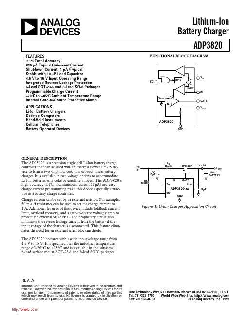
a
FEATURES ؎ 1% Total Accuracy 630 A Typical Quiescent Current Shutdown Current: 1 A (Typical) Stable with 10 F Load Capacitor 4.5 V to 15 V Input Operating Range Integrated Reverse Leakage Protection 6-Lead SOT-23-6 and 8-Lead SO-8 Packages Programmable Charge Current –20؇C to +85؇C Ambient Temperature Range Internal Gate-to-Source Protective Clamp APPLICATIONS Li-Ion Battery Chargers Desktop Computers Hand-Held Instruments Cellular Telephones Battery Operated Devices
- 1、下载文档前请自行甄别文档内容的完整性,平台不提供额外的编辑、内容补充、找答案等附加服务。
- 2、"仅部分预览"的文档,不可在线预览部分如存在完整性等问题,可反馈申请退款(可完整预览的文档不适用该条件!)。
- 3、如文档侵犯您的权益,请联系客服反馈,我们会尽快为您处理(人工客服工作时间:9:00-18:30)。
.
#The circuit diagram and others included in this specification are intended for use we take no responsibility for to explain typical application examples. Therefore, any problem as may occur due to the use of the included circuit and for any problem with industrial proprietary rights or other ridle this document carefully
LZOP3820
for it contains material protected by international copyright law. Any reproduction, full or in part, of this material is prohibited without the express written permission of the company. please observe the conditions written herein and the precautions outlined in the following paragraphs. In no event shall the company be liable for any damages resulting from failure to strictly adhere to these conditions and precautions, (1) The products covered herein are designed and manufactured for the following application areas. Vhen using the products covered herein for the equipment listed in Paragraph (2>, even for the following application areas, be sure to observe the precautions given in Paragraph CU. Never use the products for the equipment listed in Paragraph (3). *Office electronics OInstrumentation and measuring equipment #Machine tools SAudiovisual equipment *Home appliances Xommunication equipment other than for trunk lines (2) Those contemplating using the products covered herein for the following equipment which demands high reliability, should first contact a sales representative of the company and then accept responsibility for incorporating into the design fail-safe operation, redundancy, and other appropriate measures for ensuring reliability and safety of the equipment and the overall system. *Control and safety devices for airplanes, trains, automobiles, and other transportation equipment *Mainframe computers *Traffic control systems *Gas leak detectors and automatic cutoff devices ,Bescue and security equipment *Other safety devices and safety equipment,etc. (3) Do not use the products covered herein for the following equipment which demands extremely high performance in terms of functionality, reliability, accuracy. -Aerospace equipment Xcfnmunications equipment for trunk lines Control equipment for the nucJear power industry BMedical equipment related to life support, etc. (4) Please direct all queries and comments regarding above three Paragraphs to a sales representative the interpretation of the company. to a sales of the
P. 2 P. 3 P. 4 P. 5 P. 6 P. 7
P.a
p. 9 P. IO P. 13 P. 16 P. 17 P. 18 P. 20
1 1. EXAMPLE STANDARD OF OPERATING CIRCUIT ,.*..'.ll,,,*,l,ltl. 12. SPECIFICATION FORBLEMISH . . . . ..*..0..111,.1.10,11..1..
Features 1) Number of image pixels 2) 3) 4) 5) 6) 7) 8) 9) 10) : Horizontal 367 x vertical 291 (approximately 110,000 pixels) : Horizontal 5.6Pm x vertical 5.6pm
purchasing
order.
CUSTOMERS AcCEpTANCJ3 DATE: BY: PRESENTED
I Dept. General Manager
REVIEWD BY:
PREPAREDBY:
Product Development Dept. II CCD Development Center Integrated Circuits Devel SBABP CORPORATION
LZOP3820
2
LZOP3820 is a l/7-type(approx.2.6mm) The sensor further includes a timing sampling(CDS) circuit, an auto gain digital converter(ADC) circuit. All by 3.3V single power supply. Having possible to make ultra-small color
l Vhen using the products covered herein,
or
0 Please direct representative
all queries regarding of the company.
the products covered herein
元器件交易网
1 3. CAUTIONSFORUSE ,1,,1.1,11..10,,,1....‘.,,~......,.~... 14. PACKAGE OUTLINE ANDPACKING SPECIFICATI(JN Illl,,l#ll.~l*t
元器件交易网
SHARF,
l.GENERAL DESCRIPTION
元器件交易网
#’
-SHARP
SPECIFICATIONS
Product Type : l’7%FG lens-integrated CMOSColor Area Sensor for CIF
Yodel
No.
LZOP3820
%This specifications contains 24 pages including the cover. If you have any objections,please contact us before issuing
lens-integrated CMOS image sensor. generatoer(TG), a correlated double control(AGC) circuit and an analog-tothe circuits of the sensor can be driven smaI1 lens and small LCC-type flat pakage, camera easily.
Square pixel, Pixel pitch Progressive acan Compatible with CIF standard Primary color filter composed of B. G, B AnaIog output and a-bit digital output Variable electronic shutter (l/30 to l/10,000 s> Variable gain control (3 to 30 dB) Can be operating by DC3.3V single power supply 36-pin half-pitch LCC-type small pakage (Base section size: ll.5mmXll. 5mm max. ) 11) pprox. 58” (degrees) of horizontal view angle lens includes. 12) Not designed or rated as radiation hardened Applications Yireless phone camera Image capture camera for PC,PDA Amusement (Game, Toy) etc.