D8740270GT中文资料
KENWOOD TK(建伍对讲机)
KENWOOD TK-378/278 中文说明书2010-05-28 10:43建伍TK378对讲机是一种性价比较高的机型,在此介绍其编程方法及维修时的基本调整,以供维修人员参考。
编程方法1.同时按住LAMP(侧面照明灯键)和DIAL两键,接通电源,两秒钟后液晶屏显示“SEL”,即进入了经销商模式。
2.在此显示下,按TA键,进入信道频率编程状态,显示信道号数字。
3.用信道选择旋钮选择好信道号数(共有32个信道数)后,按(PTT键) 呼叫键确定,再配合键盘进入该信道数的各功能设定。
各项功能的设定依次为信道号数、接收频率、接收CTCSS频率、发射频率、发射CTCSS频率、DTMF信令、ANI功能、可否被扫描、锁定繁忙信道、时钟拍频频率偏移、发射功率、自台号码(DTMF)等功能。
4.全部的信道功能、参数设定完成后,液晶屏显示“END”,关机结束。
注意:在设定频率时,用SCN键可切换步进值(6.25kHz/5kHz);按住LAMP键再旋转信道选择钮能以1MHz的步进值变化。
维修该机时的调整同时按住LAMP和TA键,打开电源,两秒钟后进入“测试模式”,按1下TA键,再旋转信道选择钮选择好所需频率,再同时按LAMP和L0键,显示“tUnE”字符,进入调整模式。
1.调整高发射功率值及低发射功率值把功率计连接到通信机上,选择好频率后,使通信机处于显示“tUnE”状态,按住PTT键,便自动以高功率发射,此时,液晶屏显示“H---”,一边注视功率计,一边用信道选择旋钮把发射功率调整到目标值(数值在0~254可调)。
顺(逆)时针方向旋转信道选择旋转,发射功率变大(小),后按任意键,调好的数值被存入存储器中,通信机回到“tUnE”状态,再按PTT键,通信机便切换到低功率发射状态,此时显示“L---”。
2.写入接收状态“繁忙”的基准值,调整好静噪电平级3或9的数值,其他静噪电平级的值可根据3和9的数值来自动计算将信号发生器连接到通信机上,选择好频率,使通信机显示“tUnE”,输入一个希望能恰好打开9级静噪的信号电平,按住MONT键,开始进行接收,此时,显示“9---”(数值在1~255内可调)。
郎汉德 PLC 触摸屏一体机(4.3 寸) 产品说明书

郎汉德PLC触摸屏一体机(4.3寸)产品说明书文件版本:V1.0.0目录1.产品简介 (3)2.参数详情 (3)2.1.电气参数 (3)2.2.PLC编程电缆参数 (4)2.3.选型表 (6)2.4.拨码状态 (7)2.5.接线图 (8)2.5.1.晶体管输出型号引脚定义 (8)2.5.2.继电器输出型号引脚定义 (10)2.6.PLC地址 (11)2.6.1.PLC地址使用情况 (11)2.6.2.特殊寄存器和位 (12)2.7.模拟量转换 (16)2.8.兼容三菱指令 (17)3.通信使用 (21)3.1.串口通信配置 (21)3.2.一体机内部PLC与HMI通讯(COM2) (22)3.2.1.使用FX3U协议内部通讯 (22)3.2.2.使用Modbus RTU内部通讯 (25)3.3.串口通信发送与接收数据的应用(COM4) (27)3.3.1.PLC做为Modbus从站通信 (27)3.3.2.串口自由通信协议ADPRW指令使用 (28)3.3.3.Modbus主站通信协议ADPRW指令使用 (31)4.售后 (33)4.1.联系方式 (33)4.2.免责声明 (33)1.产品简介本产品为PLC触摸屏一体机。
PLC支持3U编程风格;HMI组态图库丰富。
2.参数详情2.1.电气参数类别项目参数电气环境供电电源额定24V,12-32V宽压输入范围;内部与外供电电气隔离工作温度0~55°C湿度5%-95%RH(非结露)抗干扰性峰值:1500vp-p;幅度1uS;上升时间:30ms;周期30-100HZ抗震动符合IEC61121-2标准电气隔离性能通讯隔离性通讯口均与内部隔离电源隔离性内部5V、15V之间隔离;与24V输入隔离数字量量输入导通状态高于DC15V,2.5mA 关断状态低于DC7V,1mA晶体管输出响应时间ON->OFF20us以内OFF->ON50us以内输出电压范围DC5V~30V额定输出负载0.75A@DC24V继电器输出响应时间10ms以内输出电压范围DC5V-30或AC5V~250V 额定输出电压DC24V/2A或AC220V/2.0A 使用寿命机械1千万次电气10万次(额定负载)模拟量输出输出范围电压输出0~10V 电流输出0~20mA模拟量输入输入范围电流输入0-20mA或4-20mA电压输入0-10V运动控制脉冲输出速度可达200KHZ 计数输入速度可200K以上2.2.PLC编程电缆参数一体机的PLC部分,对应的编程口为RS232通信。
zlg翻译的LPC1700中文手册
zlg翻译的LPC1700中文手册广州周立功单片机发展有限公司第1章第1章概述1.1 简介 LPC1700 系列Cortex-M3 微控制器用于处理要求高度集成和低功耗的嵌入式应用。
ARMCortex-M3 是下一代新生内核,它可提供系统增强型特性,例如现代化调试特性和支持更高级别的块集成。
LPC1700 系列 Cortex-M3 微控制器的操作频率可达 100MHz。
ARM Cortex-M3 CPU 具有 3级流水线和哈佛结构,带独立的本地指令和数据总线以及用于外设的稍微低性能的第三条总线。
ARM Cortex-M3 CPU 还包含一个支持随机跳转的内部预取指单元。
LPC1700 系列 Cortex-M3 微控制器的外设组件包含高达512KB 的 Flash 存储器、64KB 的数据存储器、以太网 MAC、 USB 主机/从机/OTG 接口、通道的通用 DMA 控制器、个 UART、 8 4 2 22 条 CAN 通道、2 个 SSP 控制器、SPI 接口、3 个 I C 接口、2-输入和 2-输出的 I S 接口、8 通道的 12 位 ADC、10 位 DAC、电机控制 PWM、正交编码器接口、4 个通用定时器、6-输出的通用 PWM、带独立电池供电的超低功耗 RTC 和多达 70 个的通用 I/O 管脚。
1.2 特性 ARM Cortex-M3 处理器,可在高至 100MHz 的频率存储器保护单元(MPU) ; ARM Cortex-M3 下运行,并包含一个支持 8 个区的内置了嵌套的向量中断控制器(NVIC) ; 具有在系统编程(ISP)和在应用编程(IAP)功能的 512KB 片上 Flash 程序存储器。
把增强型的 Flash 存储加速器和Flash 存储器在 CPU 本地代码/数据总线上的位置进行整合,则 Flash 可提供高性能的代码; 64KB 片内 SRAM 包括: –32KB SRAM 可供高性能 CPU 通过本2 个 16KB SRAM 模块,带独立访问路径,可进行更高地代码/数据总线访问; –吞量的操作。
艾顿278480产品说明书
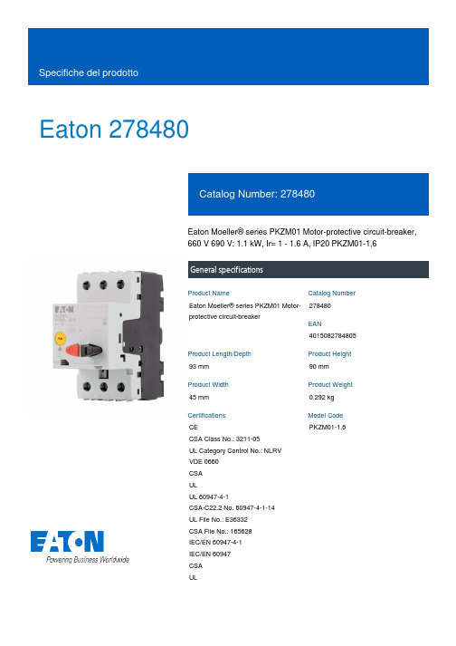
Eaton 278480Eaton Moeller® series PKZM01 Motor-protective circuit-breaker,660 V 690 V: 1.1 kW, Ir= 1 - 1.6 A, IP20 PKZM01-1,6General specificationsEaton Moeller® series PKZM01 Motor-protective circuit-breaker278480401508278480593 mm90 mm45 mm0.292 kgCECSA Class No.: 3211-05UL Category Control No.: NLRV VDE 0660CSAULUL 60947-4-1CSA-C22.2 No. 60947-4-1-14 UL File No.: E36332CSA File No.: 165628IEC/EN 60947-4-1IEC/EN 60947CSAUL PKZM01-1,6Product Name Catalog NumberEANProduct Length/Depth Product Height Product Width Product Weight Certifications Model Code1.6 A2 x (1 - 6) mm², ferrule to DIN 462281 x (1 - 6) mm², ferrule to DIN 46228Is the panel builder's responsibility. The specifications for the switchgear must be observed.25 °C0.55 kWMeets the product standard's requirements.Is the panel builder's responsibility. The specifications for the switchgear must be observed.Does not apply, since the entire switchgear needs to be evaluated.1.6 A (3 contacts in series), DC-5 up to 250V1.6 A, AC-3 up to 440 V10 mm40 °C50 kAMeets the product standard's requirements.40 °C25 A eaton-manual-motor-starters-characteristic-characteristic-curve-008.eps eaton-manual-motor-starters-characteristic-characteristic-curve-006.epsDA-DC-00004884.pdfDA-DC-00004914.pdfETN.PKZM01-1,6IL122023ZUIL03407011ZIL122012ZUIL03402034ZDA-CD-pkzm01DA-CS-pkzm01Rated operational current for specified heat dissipation (In) Terminal capacity (flexible with ferrule)10.11 Short-circuit ratingAmbient operating temperature (enclosed) - minRated operational power at AC-3, 380/400 V, 50 Hz10.4 Clearances and creepage distances10.12 Electromagnetic compatibility10.2.5 LiftingSwitching capacityStripping length (main cable)Ambient operating temperature (enclosed) - maxRated short-circuit breaking capacity Icu at 400 V AC 10.2.3.1 Verification of thermal stability of enclosures Ambient storage temperature - minAdjustment range undelayed short-circuit release - max 10.8 Connections for external conductors Characteristic curve Declarations of conformity eCAD modelGuide utenteIstruzioni di installazione mCAD modelIs the panel builder's responsibility.Assigned motor power at 575/600 V, 60 Hz, 3-phase0.75 HPProtectionFinger and back-of-hand proof, Protection against direct contact when actuated from front (EN 50274)Actuator typePush buttonRated operational power at AC-3, 440 V, 50 Hz0.55 kWAmbient operating temperature - max55 °CRated operational power at AC-3, 220/230 V, 50 Hz0.25 kWClimatic proofingDamp heat, constant, to IEC 60068-2-78Damp heat, cyclic, to IEC 60068-2-30Device constructionBuilt-in device fixed built-in techniqueFeaturesPhase-failure sensitivity (according to IEC/EN 60947-4-1, VDE 0660 Part 102)Lifespan, electrical50,000 operations (at 400V, AC-3)Static heat dissipation, non-current-dependent Pvs0 WElectrical connection type of main circuitScrew connection10.9.3 Impulse withstand voltageIs the panel builder's responsibility.Number of polesThree-poleAmbient operating temperature - min-25 °C10.6 Incorporation of switching devices and componentsDoes not apply, since the entire switchgear needs to be evaluated.10.5 Protection against electric shockDoes not apply, since the entire switchgear needs to be evaluated.Mounting positionCan be snapped on to IEC/EN 60715 top-hat rail with 7.5 or15 mm height.Rated uninterrupted current (Iu)1.6 ATripping characteristicOverload trigger: tripping class 10 AShort-circuit release24.8 A, Irm, Setting range max.Basic device fixed 15.5 x Iu, Trip Blocks± 20% tolerance, Trip blocks10.13 Mechanical functionThe device meets the requirements, provided the information in the instruction leaflet (IL) is observed.10.2.6 Mechanical impactDoes not apply, since the entire switchgear needs to be evaluated.10.9.4 Testing of enclosures made of insulating materialIs the panel builder's responsibility.10.3 Degree of protection of assembliesDoes not apply, since the entire switchgear needs to be evaluated.Heat dissipation per pole, current-dependent Pvid1.79 WOperating frequency25 Operations/hProduct categoryMotor protective circuit breakerOverload release current setting - min1 AEquipment heat dissipation, current-dependent Pvid5.36 WHeat dissipation capacity Pdiss0 WRated operational current (Ie)1.6 AAssigned motor power at 460/480 V, 60 Hz, 3-phase0.75 HPSuitable forAlso motors with efficiency class IE3Branch circuit: Manual type E if used with terminal, or suitable for group installations, (UL/CSA)Internal resistance700 mΩTemperature compensation-25 - 55 °C, Operating range≤ 0.25 %/K, residual error for T > 40°-5 - 40 °C to IEC/EN 60947, VDE 0660Terminal capacity (solid)1 x (1 - 6) mm²2 x (1 - 6) mm²Rated frequency - min50 HzShort-circuit current60 kA DC, up to 250 V DC, Main conducting pathsPower loss5.36 W10.2.3.2 Verification of resistance of insulating materials to normal heatMeets the product standard's requirements.10.2.3.3 Resist. of insul. mat. to abnormal heat/fire by internal elect. effectsMeets the product standard's requirements.Lifespan, mechanical50,000 Operations (Main conducting paths)Terminal capacity (solid/stranded AWG)18 - 10Overload release current setting - max1.6 A10.9.2 Power-frequency electric strengthIs the panel builder's responsibility.Overvoltage categoryIIIDegree of protectionTerminals: IP00IP20Rated frequency - max60 HzSwitch off techniqueThermomagneticAmbient storage temperature - max80 °CAdjustment range undelayed short-circuit release - min25 APollution degree310.7 Internal electrical circuits and connectionsIs the panel builder's responsibility.Rated impulse withstand voltage (Uimp)6000 V ACConnectionScrew terminals10.10 Temperature riseThe panel builder is responsible for the temperature rise calculation. Eaton will provide heat dissipation data for the devices.FunctionsPhase failure sensitiveMotor protectionTightening torque1.7 Nm, Screw terminals, Main cableRated operational voltage (Ue) - min690 VAssigned motor power at 230/240 V, 60 Hz, 1-phase0.1 HP10.2.2 Corrosion resistanceMeets the product standard's requirements.10.2.4 Resistance to ultra-violet (UV) radiationMeets the product standard's requirements.10.2.7 InscriptionsMeets the product standard's requirements.Shock resistance25 g, Mechanical, according to IEC/EN 60068-2-27, Half-Eaton Corporation plc Eaton House30 Pembroke Road Dublin 4, Ireland © 2023 Eaton. Tutti i diritti riservati. Eaton is a registered trademark.All other trademarks areproperty of their respectiveowners./socialmediasinusoidal shock 10 ms690 V Max. 2000 mRated operational voltage (Ue) - max Altitude。
BDA4700 Datasheet说明书
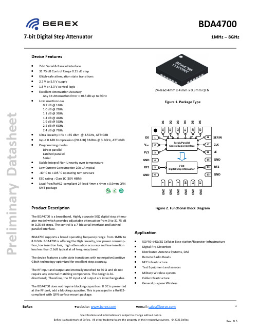
7-bit Digital Step Attenuator 1MHz – 8GHzP r e l i m i n a r y D a t a s h e e tDevice Features24-lead 4mm x 4 mm x 0.9mm QFN• 7-bit Serial & Parallel Interface • 31.75 dB Control Range 0.25 dB step • Glitch -safe attenuation state transitions • 2.7 V to 5.5 V supply • 1.8 V or 3.3 V control logic•Excellent Attenuation AccuracyAny bit Attenuation Error < ±0.5 dB up to 6GHz • Low Insertion Loss 0.7 dB @ 1GHz 1.0 dB @ 2GHz 1.1 dB @ 3GHz 1.4 dB @ 4GHz 1.9 dB @ 5GHz 2.5 dB @ 6GHz 2.4 dB @ 7GHz• UltralinearityIIP3>+************,ATT=0dB• Input0.1dBCompression(P0.1dB)************,ATT=0dB•Programming modes Direct parallel Latched parallel Serial• Stable Integral Non -Linearity over temperature• Low Current Consumption 200 μA typical • -40 °C to +105 °C operating temperature • ESD rating : Class1C (1KV HBM)•Lead -free/RoHS2-compliant 24-lead 4mm x 4mm x 0.9mm QFN SMT packageApplication• 5G/4G+/4G/3G Cellular Base station/Repeater Infrastructure • Digital Pre -Distortion• Distributed Antenna Systems, DAS • Remote Radio Heads • NFC Infrastructure • Test Equipment and sensors • Military Wireless system • Cable Infrastructure •General purpose WirelessProduct DescriptionThe BDA4700 is a broadband, Highly accurate 50Ω digital step attenu-ator model which provides adjustable attenuation from 0 to 31.75 dB in 0.25 dB steps. The control is a 7-bit serial interface and latched parallel interface.BDA4700 supports a broad operating frequency range from 1MHz to 8.0 GHz. BDA4700 is offering the High linearity, low power consump-tion, low insertion loss, high attenuation accuracy and low insertion loss less than 2.6dB typical at all frequency band.The device features a safe state transitions with no negative/positive Glitch technology optimized for excellent step accuracy.The RF input and output are internally matched to 50 Ω and do not require any external matching components. The design is bi -directional; Therefore, the RF input and output are interchangeable.The BDA4700 does not require blocking capacitors. If DC is presented at the RF port, add a blocking capacitor. This is packaged in a RoHS2-compliant with QFN surface mount package.Figure 2. Functional Block DiagramFigure 1. Package TypeD0V DD P/S GND RF1GNDG N DG N DG N DG N DG N DG N DSERIN CLK LE GND RF2GNDD 1D 2D 3D 4D 5D 67-bit Digital Step Attenuator 1MHz – 8GHzP r e l i m i n a r y D a t a s h e e tTable 1. Electrical Specifications 17-bit Digital Step Attenuator 1MHz – 8GHzP r e l i m i n a r y D a t a s h e e tTable 2. Recommended operating ConditionTable 3. Absolute Maximum RatingsTable 1. Electrical Specifications 1(Cont.)7-bit Digital Step Attenuator 1MHz – 8GHzP r e l i m i n a r y D a t a s h e e t1. RF pins 5 and 14 must be at 0V DC. The RF pins do not require DC blocking capacitors for proper Operation if the 0V DC requirement is met2. Ground D0 - D6 if not used or serial mode.D0V DD P/SGND RF1GNDG N DG N DG N DG N DG N DG N DSERIN CLK LE GND RF2GNDD 1D 2D 3D 4D 5D 6Figure 3. Pin Configuration (Top View)Table 4. Pin Description7-bit Digital Step Attenuator 1MHz – 8GHzP r e l i m i n a r y D a t a s h e e tProgramming OptionsBDA4700 can be programmed using either the parallel or serial inter-face, which is selectable via P/S pin(Pin3).Serial mode is selected by pulling it to a voltage logic HIGH and paral-lel mode is selected by setting P/S to logic LOWSerial Control ModeThe serial interface is a 7-bit shift register to shift in the data LSB (D0) first. When serial programming is used, It is recommended all the parallel control input pins (D0-D6) are grounded.It is controlled by three CMOS -compatible signals: SERIN, Clock, and Latch Enable (LE).The BDA4700 has a 3-wire serial peripheral interface (SPI): serial data input (SERIN), clock (CLK), and latch enable (LE). The serial control interface is activated when P/S is set to HIGH.In serial mode, the 7-bit SERIN data is clocked LSB first on the rising CLK edges into the shift register and then LE must be toggled HIGH to latch the new attenuation state into the device. LE must be set to LOW to clock new 7-bit data into the shift register because CLK is masked to prevent the attenuator value from changing if LE is kept HIGH (see Figure 4 and Table 5).In serial mode operation, both the serial control inputs (LE,CLK,SERIN) and the parallel control inputs (D0 to D6)must always be kept at a valid logic level (V CTLH or V CTLL ) and must not be left floating. It is rec-ommended to connect the parallel control inputs to ground and to use pull -down resistors on all serial control input lines if the device driving these input lines goes high impedance during hiberna-tion.P/SSERIAL IN CLKLESerial bit D[7] must be set to logic lowBits can either be set to logic high or logic low Figure 4. Serial Mode Resister Timing DiagramTable 7. Truth Table for Serial Control WordTable 5. Mode SelectionTable 6. Serial Interface Timing Specifications7-bit Digital Step Attenuator 1MHz – 8GHzP r e l i m i n a r y D a t a s h e e tPower -UP states SettingsThe BDA4700 will always initialize to the maximum attenuation setting (31.75 dB) on power -up for both the Serial and Latched Parallel modes of operation and will remain in this setting until the user latches in the next programming word.In Direct Parallel mode, the DSA can be preset to any state within the 31.75 dB range by pre -setting the Parallel control pins prior to power -up. In this mode, there is a 400 μs delay between the time the DSA is powered -up to the time the desired state is set.Figure 6. Default Register SettingsSerial Register MapThe BDA4700 can be programmed via the serial control on the rising edge of Latch Enable (LE) which loads the last 8-bits data word in the SHIFT Register. Serial Data is clocked in LSB(D0) first.LSBMSB 8- Bit Atteunuation WordBits must be to logic lowFigure 5. Serial Register MapThe attenuation word is derived directly from the value of the attenuation state. To find the attenuation word, multiply the value of the state by four, then convert to binary.For example, to program the 15.75dB state : 4 x 15.75 = 63 63 -> 00111111Serial Input : 001111118- Bit Atteunuation Word7-bit Digital Step Attenuator 1MHz – 8GHzP r e l i m i n a r y D a t a s h e e tParallel Control ModeThe parallel control interface has seven digital control input lines (D6 to D0) to set the attenuation value. D6 is the most significant bit (MSB) that selects the 16 dB attenuator stage, and D0 is the least significant bit (LSB) that selects the 0.25 dB attenuator stage (see Figure 7).Direct Parallel ModeFor direct parallel mode, The LE pin must be kept HIGH. The attenua-tion state is changed by the control voltage inputs (D0 to D6) directly. This mode is ideal for manual control of the attenuator. In this mode the device will immediately react to any voltage changes to the paral-lel control pins [pins 1, 19, 20, 21,22, 23, 24]. Use direct parallel mode for the fastest settling time. (refer to page 21)Latched Parallel ModeThe LE pin must be kept LOW when changing the control voltageinputs (D0 to D6) to set the attenuation state. When the desired state is set, LE must be toggled HIGH to transfer the 7-bit data to the by-pass switches of the attenuator array, and then toggled LOW to latch the change into the device until the next desired attenuation change (see Figure 7 and Table 8).Figure 7. Latched Parallel Mode Timing DiagramTable 8. Truth Table for the Parallel Control WordTable 9. Parallel Interface Timing SpecificationsProgramming Options▪ Set P/S is logic LOW. ▪ Set LE to logic LOW.▪ Adjust pins [1, 19, 20, 21,22, 23, 24] to the desired attenuation setting. (Note the device will not react to these pins while LE is a logic LOW).▪ Pull LE to a logic HIGH. The device will then transition to the attenuation settings reflected by pins D6 - D0.▪ If LE is pulled to a logic LOW then the attenuator will not change state.Latched Parallel Mode implies a default state for when the device is first powered up with P/S pin set for logic LOW and LE logic LOW. In this case the default setting is Maximum attenuation .Glitch -Safe Attenuation State TransientThe BDA4700 is the latest product applied Glitch -Safe technology with less than 1dB ringing (pos/neg) across the attenuation range when changing attenuation states. This technology protects Amplifiers or ADC during transitions between attenuation states. (see Figure 40,41).Switching Feature DescriptionP/SParallel IN [D6:D0]LEBits can either be set to logic high or logic low7-bit Digital Step Attenuator 1MHz – 8GHzP r e l i m i n a r y D a t a s h e e tFigure 8. Typical Performance Data @ 25°C and V DD = 3.3V, EVKit RF connector and board losses are de -embedded, unless otherwise notedInsertion loss vs TemperatureFigure 9. Insertion loss vs Attenuation Setting7-bit Digital Step Attenuator 1MHz – 8GHzP r e l i m i n a r y D a t a s h e e tFigure 10.Input Return Loss vs Attenuation SettingFigure 11. Output Return Loss vs Attenuation SettingTypical Performance Data @ 25°C and V DD = 3.3V, EVKit RF connector and board losses are de -embedded, unless otherwise noted7-bit Digital Step Attenuator 1MHz – 8GHzP r e l i m i n a r y D a t a s h e e tFigure 12.Input Return Loss for 16dB Attenuation Setting vs TemperatureFigure 13. Output Return Loss for 16dB Attenuation Setting vs TemperatureTypical Performance Data @ 25°C and V DD = 3.3V, EVKit RF connector and board losses are de -embedded, unless otherwise noted7-bit Digital Step Attenuator 1MHz – 8GHzP r e l i m i n a r y D a t a s h e e tFigure 14.Relative Phase Error vs Attenuation SettingFigure 15. Relative Phase Error for 31.75dB Attenuation Setting vs FrequencyTypical Performance Data @ 25°C and V DD = 3.3V, EVKit RF connector and board losses are de -embedded, unless otherwise noted7-bit Digital Step Attenuator 1MHz – 8GHzP r e l i m i n a r y D a t a s h e e tFigure 16.Attenuation Error @900MHz vs TemperatureFigure 17. Attenuation Error @1800MHz vs TemperatureTypical Performance Data @ 25°C and V DD = 3.3V, EVKit RF connector and board losses are de -embedded, unless otherwise noted7-bit Digital Step Attenuator 1MHz – 8GHzP r e l i m i n a r y D a t a s h e e tFigure 18.Attenuation Error @2200MHz vs TemperatureFigure 19. Attenuation Error @3500MHz vs TemperatureTypical Performance Data @ 25°C and V DD = 3.3V, EVKit RF connector and board losses are de -embedded, unless otherwise noted7-bit Digital Step Attenuator 1MHz – 8GHzP r e l i m i n a r y D a t a s h e e tFigure 20.Attenuation Error @4600MHz vs TemperatureFigure 21. Attenuation Error @5800MHz vs TemperatureTypical Performance Data @ 25°C and V DD = 3.3V, EVKit RF connector and board losses are de -embedded, unless otherwise noted7-bit Digital Step Attenuator 1MHz – 8GHzP r e l i m i n a r y D a t a s h e e tFigure 22.IIP3 @ 2500MHz vs TemperatureFigure 23. IIP3 @ 3500MHz vs TemperatureTypical Performance Data @ 25°C and V DD = 3.3V, EVKit RF connector and board losses are de -embedded, unless otherwise noted7-bit Digital Step Attenuator 1MHz – 8GHzP r e l i m i n a r y D a t a s h e e tFigure 24.IIP3 @ 4500MHz vs TemperatureFigure 25. IIP3 @ 6400MHz vs TemperatureTypical Performance Data @ 25°C and V DD = 3.3V, EVKit RF connector and board losses are de -embedded, unless otherwise noted7-bit Digital Step Attenuator 1MHz – 8GHzP r e l i m i n a r y D a t a s h e e tFigure 26.IIP3 @ 7250MHz vs TemperatureFigure 27. Input 0.1dB Compression @2500MHz vs TemperatureTypical Performance Data @ 25°C and V DD = 3.3V, EVKit RF connector and board losses are de -embedded, unless otherwise noted7-bit Digital Step Attenuator 1MHz – 8GHzP r e l i m i n a r y D a t a s h e e tFigure 28.Input 0.1dB Compression @3500MHz vs TemperatureTypical Performance Data @ 25°C and V DD = 3.3V, EVKit RF connector and board losses are de -embedded, unless otherwise noted7-bit Digital Step Attenuator 1MHz – 8GHzP r e l i m i n a r y D a t a s h e e tFigure 30.Input 0.1dB Compression @5500MHz vs TemperatureFigure 31. Input 0.1dB Compression @7250MHz vs TemperatureTypical Performance Data @ 25°C and V DD = 3.3V, EVKit RF connector and board losses are de -embedded, unless otherwise noted7-bit Digital Step Attenuator 1MHz – 8GHzP r e l i m i n a r y D a t a s h e e tFigure 32.0.25dB Step Attenuation vs FrequencyFigure 33. 0.25dB Step Actual Attenuation vs FrequencyTypical Performance Data @ 25°C and V DD = 3.3V, EVKit RF connector and board losses are de -embedded, unless otherwise noted7-bit Digital Step Attenuator 1MHz – 8GHzP r e l i m i n a r y D a t a s h e e tFigure 34.Major State Bit Error vs Attenuation SettingFigure 35. 0.25dB Step Attenuation Error vs FrequencyTypical Performance Data @ 25°C and V DD = 3.3V, EVKit RF connector and board losses are de -embedded, unless otherwise noted7-bit Digital Step Attenuator 1MHz – 8GHzP r e l i m i n a r y D a t a s h e e tFigure 36.1dB Step Attenuation vs FrequencyFigure 37. 1dB Step Actual Attenuation vs FrequencyTypical Performance Data @ 25°C and V DD = 3.3V, EVKit RF connector and board losses are de -embedded, unless otherwise noted7-bit Digital Step Attenuator 1MHz – 8GHzP r e l i m i n a r y D a t a s h e e tFigure 38.1dB Major State Bit Error vs Attenuation SettingFigure 39. 1dB Major Attenuation Error vs FrequencyTypical Performance Data @ 25°C and V DD = 3.3V, EVKit RF connector and board losses are de -embedded, unless otherwise noted7-bit Digital Step Attenuator 1MHz – 8GHzP r e l i m i n a r y D a t a s h e e tFigure 40.Attenuation Transient (15.75 to 16dB, Pin=18dBm)Figure 41. Attenuation Transient (16 to 15.75dB, Pin=18dBm)Glitch = 0.21dBTypical Performance Data @ 25°C and V DD = 3.3V, EVKit RF connector and board losses are de -embedded, unless otherwise notedGlitch = 0.15dB7-bit Digital Step Attenuator 1MHz – 8GHzP r e l i m i n a r y D a t a s h e e tEvaluation board Kit IntroductionBDA4700 Evaluation Kit is made up of a combination of an RF board and an interface boardThe schematic of the BDA4700 evaluation RF board is shown in Figure 34. The BDA4700 evalu-ation RF board is constructed of a 4-layer material with a copper thickness of 0.7 mil on each layer. Every copper layer is separated with a dielectric material. The top dielectric material is 8 mils RO4003. The middle and bottom dielectric materials are FR -4, used for mechanical strength and overall board thickness of approximately 1.63mm.BDA4700 Evaluation INTERFACE board is assembled with a SP3T switches(D0~D6,LE), SP2T mechanical switch (P/S), and several header & switch.Evaluation Board Programming Using USB InterfaceIn order to evaluate the BDA4700 performance, the Application Software has to be installed on your computer. And The DSA application software GUI supports Latched Parallel and Serial modes . software can be downloaded from BeRex ’s websiteSerial Control Mode• Connect directly the Evaluation INTEFRACE board USB port(J3) to PC • Set the direction of P<->S Switch to S direction (P/S Logic HIGH) • Set the D0~D6, LE switch to the middle position.• Operate the 0~31.75dB attenuation state in GUI and then control the DSALatched Parallel Control Mode• Connect directly the Evaluation INTEFRACE board USB port(J3) to PC • Set the direction of P<->S Switch to P direction (P/S Logic LOW) • Set the D0~D6, LE switch to the middle position.•Operate the 0~31.75dB attenuation state in GUI and then control the DSADirect Parallel Control Mode• Set the direction of P<->S Switch to P direction (P/S Logic LOW) • Set LE switch to the LOW Position•For the setting to attenuation state, D0~D6 switches can be combined in manually pro-gram, refer to Table 9.Please refer to user manual for more detailed operation method of BDA4700 EVK.Figure 42. BDA4700 EVK7-bit Digital Step Attenuator 1MHz – 8GHzP r e l i m i n a r y D a t a s h e e tSERIN/D6LECLK/D5Figure 44. Evaluation Board PCB Layout Information 50ΩTable 10. Bill of Material - Evaluation BoardFigure 45. Evaluation Board PCB Layer Information 50ΩTOPBOTTOMFigure 43. Evaluation Board Kit Schematic Diagram7-bit Digital Step Attenuator 1MHz – 8GHzP r e l i m i n a r y D a t a s h e e tFigure 46. Recommended Serial mode Application Circuit SchematicNote: 1. C1 and C2 should be placed near the device.2. Recommended to add pull -down resistor at the LE pin.SERIN VDDP/S LECLK7-bit Digital Step Attenuator 1MHz – 8GHzP r e l i m i n a r y D a t a s h e e tFigure 47. NOTE :1. Dimensioning and tolerancing conform to ASME Y14.5-2009.2. All dimensions are in millimeters.3. N is the total number of terminals.4. The location of the marked terminal #1 identifier is within the hatched area.5. ND and NE refer to the number of terminals on each D and E side respectively.6. Dimension b applies to the metallized terminal and is measured between 0.15mm and 0.30mm from the terminal tip. If the terminal has a radius on the other end of it, dimension b should not be meas-ured in that radius area.7. Coplanarity applies to the terminals and all other bottom surface metallizationPacking Outline DimensionTOP VIEW7-bit Digital Step Attenuator 1MHz – 8GHzP r e l i m i n a r y D a t a s h e e tFigure 48. Recommend Land PatternFigure 49. Package Marking7-bit Digital Step Attenuator 1MHz – 8GHzP r e l i m i n a r y D a t a s h e e tFigure 50. Tape & ReelPackaging information:[Unit: MM]31 Rev. 0.5 BeRex ●website: ●email: ***************Specifications and information are subject to change without notice. BeRex is a trademark of BeRex. All other trademarks are the property of their respective owners. © 2021 BeRex 7-bit Digital Step Attenuator 1MHz – 8GHzBDA4700P r e l i m i n a r y D a t a s h e e t Lead plating finish100% Tin Matte finish(All BeRex products undergoes a 1 hour, 150 degree C, Anneal bake to eliminate thin whisker growth concerns.)MSL / ESD RatingESD Rating:Value:Test:Standard:ESD Rating:Value:Test:Standard:MSL Rating:Standard: Class 1C 1000V Human Body Model (HBM) JEDEC Standard JS -001-2017 Class C4 1000V Charged Device Model (CDM) JEDEC Standard JESD22-C101F Level 1 at +260°C convection reflow JEDEC Standard J -STD -020NATO CAGE code:Proper ESD procedures should be followed when handling this device.C a u t i o n : ESD Sensitive Appropriate precautions in handling, packaging and testing devices must be observed.RoHS Compliance This part is compliant with Restrictions on the use of certain Hazardous Substances in Electrical and Electronic Equipment (RoHS) Directive 2011/65/EU as amended by Directive 2015/863/EU. This product also is compliant with a concentration of the Substances of Very High Concern (SVHC) candidate list which are contained in a quantity of less than 0.1%(w/w) in each components of a product and/or its packaging placed on the European Community mar-ket by the BeRex and Suppliers.。
HPMLDL系列服务器

HPMLDL系列服务器hpML系列服务器HP ProLiant ML110G7(C8R00A)参数规格差不多参数产品类型工作组级产品类别塔式产品结构4U处理器CPU类型奔腾双核CPU型号奔腾双核G860CPU频率3GHzHP ProLiant ML330 G6(600911-AA1)参数规格差不多参数产品类型企业级产品类别塔式产品结构5U处理器CPU类型Intel 至强5600CPU型号Xeon E5620CPU频率 2.4GHz智能加速主2.666GHz频标配CPU1颗数量最大CPU2颗数量制程工艺32nm三级缓存12MB总线规格QPI 5.86GT/sCPU核心四核HP ProLiant ML330 G6(B9D22A)参数规格差不多参数产品类型企业级产品类别塔式产品结构5U处理器CPU类型Intel 至强5600 CPU型号Xeon E5606CPU频率 2.13GHz标配CPU1颗数量最大CPU2颗数量制程工艺32nm三级缓存8MB总线规格QPI 4.8GT/sHP ProLiant ML330 G6(600911-AA1)参数规格差不多参数产品类型企业级产品类别塔式产品结构5U处理器CPU类型Intel 至强5600CPU型号Xeon E5620CPU频率 2.4GHz智能加速主2.666GHz频标配CPU1颗数量最大CPU2颗数量制程工艺32nm三级缓存12MB总线规格QPI 5.86GT/sCPU核心四核HP ProLiant ML350 G6(638180-AA1)参数规格差不多参数产品类别塔式产品结构5U处理器CPU类型Intel 至强5600CPU型号Xeon E5606CPU频率 2.13GHz标配CPU1颗数量最大CPU2颗数量制程工艺32nm三级缓存8MB总线规格QPI 4.8GT/sCPU核心四核CPU线程四线程数主板HP ProLiant ML350 G6(600431-AA5)参数规格差不多参数产品类别塔式产品结构5U处理器CPU类型Intel 至强5600CPU型号Xeon E5620CPU频率 2.4GHz智能加速主2.666GHz频标配CPU1颗数量最大CPU2颗数量制程工艺32nm三级缓存12MB总线规格QPI 5.86GT/sCPU核心四核CPU线程八线程数HP ProLiant ML350 G6(594869-AA1)参数规格差不多参数产品类别塔式产品结构5U处理器CPU类型Intel 至强5600CPU型号Xeon E5620CPU频率 2.4GHz智能加速主2.666GHz频标配CPU1颗数量最大CPU2颗数量制程工艺32nm三级缓存12MB总线规格QPI 5.86GT/sCPU核心四核CPU线程八线程数HP ProLiant ML310e Gen8(686146-AA5)参数规格差不多参数产品类型企业级产品类别塔式产品结构4U处理器CPU类型Intel 至强E3-1200 v2 CPU型号Xeon E3-1220 v2CPU频率 3.1GHz标配CPU1颗数量最大CPU4颗数量制程工艺22nm三级缓存8MB总线规格DMI 5GT/sHP ProLiant ML310e Gen8(686147-AA5)参数规格差不多参数产品类型企业级产品类别塔式产品结构4U处理器CPU类型Intel 至强E3-1200 v2 CPU型号Xeon E3-1240 v2CPU频率 3.4GHz智能加速主3.8GHz频标配CPU1颗数量最大CPU4颗数量制程工艺22nm三级缓存8MBHP ProLiant ML350e Gen8(C3Q10A)参数规格差不多参数产品类型企业级产品类别塔式产品结构5U处理器CPU类型Intel 至强E5-2400 CPU型号Xeon E5-2403CPU频率 1.8GHz标配CPU1颗数量最大CPU4颗数量制程工艺32nm三级缓存10MB总线规格QPI 6.4GT/sHP ProLiant ML350e Gen8(C3Q08A)参数规格差不多参数产品类型企业级产品类别塔式产品结构5U处理器CPU类型Intel 至强E5-2400 CPU型号Xeon E5-2407CPU频率 2.2GHz标配CPU1颗数量最大CPU4颗数量制程工艺32nm三级缓存10MB总线规格QPI 6.4GT/sHP ProLiant ML350e Gen8(C3Q09A)参数规格差不多参数产品类型企业级产品类别塔式产品结构5U处理器CPU类型Intel 至强E5-2400 CPU型号Xeon E5-2420CPU频率 1.9GHz标配CPU1颗数量最大CPU4颗数量制程工艺32nm三级缓存15MB总线规格QPI 6.4GT/sHP ProLiant ML350e Gen8(C3F91A)参数规格差不多参数产品类型企业级产品类别塔式产品结构5U处理器CPU类型Intel 至强E5-2400 CPU型号Xeon E5-2430CPU频率 2.2GHz标配CPU1颗数量最大CPU4颗数量制程工艺32nm三级缓存15MB总线规格QPI 6.4GT/sHP ProLiant ML350p Gen8(646675-AA1)参数规格差不多参数产品类别塔式产品结构5U处理器CPU类型Intel 至强E5-2600 CPU型号Xeon E5-2609CPU频率 2.4GHz标配CPU1颗数量最大CPU2颗数量制程工艺32nm三级缓存10MB总线规格QPI 6.4GT/sHP ProLiant ML350p Gen8(668271-AA5)参数规格差不多参数产品类别塔式产品结构5U处理器CPU类型Intel 至强E5-2600 CPU型号Xeon E5-2620CPU频率2GHz智能加速主2.5GHz频标配CPU1颗数量最大CPU2颗数量制程工艺32nm。
Agilent I O Hardware 数据手册说明书
82357A technical specificationsGeneral requirementsMinimum system requirements Windows 98(SE)/Me 2•PCI IEEE-488 interface for PCs•Transfer rates up to 900 KB/s•Dual processor support onWindows 2000/XPBest for•Maximum GPIB throughput forall configurationsHigh performance for manufacturingtest applicationsThe 82350B is Agilent’s highest-performance GPIB interface. Witha direct PCI computer connection,transaction overhead is minimizedfor the best overall performance.The 82350B card de-couples GPIBtransfers from PCI bus transfers.Buffering provides I/O and systemperformance that is superior to directmemory access (DMA). The hardwareis software configurable and compati-ble with the Plug-and-Play standardfor easy hardware installation. TheGPIB interface card plugs into a 5 voltPCI slot in the backplane of your PC.For programming capability youhave access with the latest versionof IO Libraries suite, version 14.1, toprogram in all standard developmentenvironments. Agilent’s IO LibrariesSuite 14.1 is easy to use and workswith virtually any vendor’s instrumentor T&M programming softwareapplication and includes automaticconfiguration for Agilent or NI VISA,NI-488.2, VISA COM or T&M ToolkitDirect IO. Even if you use NI IO soft-ware Agilent will configure automati-cally so as a user you do not have tobe concerned with the behind-the-scenes details.382350B technical specifications General requirements Minimum system requirements Windows 98(SE)/Me (note 98 supported with version 14.0 only)/2000/XP Software required Agilent IO Libraries Suite (included); see requirements on page 1PCI bus slot 5-V PCI slot, 32 bits Supported standards PCI rev 2.2IEEE 488.1 and IEEE 488.2 compatible General characteristics Power Backplane +5 V PCI Connectors Standard 24-pin GPIB (IEEE-488)+5V PCI Maximum data rate More than 900 KB/s Maximum instrument connection 14 instruments—daisy chain via GPIB Buffering Built-in Configuration Plug-and-Play EMC and safety *IEC 61326-1Group 1, Class A IEC 61010-1Warranty 1 year Dimensions Length, width, and height 122 mm (L) x 122 mm (W) x 22 mm (H) (a full-height PCI card)Weight 0.091 kg Environmental specifications Operating environment 0°C to 55°C Operating humidity Up to 90% at 40°C non-condensing Storage environment -40°C to +70°C Storage humidity Up to 90% at 65°C non-condensing * Additional detail and information in the Declaration of ConformityThis traditional GPIB connection still offers the highest throughputE5810A technical specifications 45USB port on your PC to up to fourRS-232 instruments or devices•Fully compatible with WindowsCOM driver and industry-standardVISA I/O software.Best for•Easy connection to RS-232 devices•Notebook computer RS-232connectionsAdd four serial ports in minutesThe Agilent E5805A USB/4-portRS232 interface provides a directconnection from the USB port onyour notebook or desktop PC to up tofour RS-232 instruments or devices.There are no switches to set, no PCcards to install, and no external powersupplies are required. Simply installthe driver and plug in the E5805AUSB 4-port RS232 interface to addfour RS-232 ports to your computer.Since the E5805A is a standardPlug-and-Play device, your computerautomatically detects and configuresit when it is connected to your com-puter USB port. You can interface upto four devices, with baud rates up to230 Kb/s per serial port. The E5805Aprovides four DB9 serial connectorsand ships with a 1.8-meter USB cable.E5813A technical specificationsGeneral requirements67Agilent Technologies’ Test and Measurement Support, Services, and Assistance Agilent Technologies aims to maximize the value you receive, while minimizing your risk and problems. We strive to ensure that you get the test and measurement capabilities you paid for and obtain the support you need. Our extensive support resources and services can help you choose the right Agilent products for your applications and apply them successfully. Every instru-ment and system we sell has a global warranty. Support is available for at least five years beyond the production life of the product. Two concepts underlie Agilent’s overall support policy: “Our Promise” and “Your Advantage.”Our Promise Our Promise means your Agilent test and measurement equipment will meet its advertised performance and functionality. When you are choosing new equipment,we will help you with product information, including realistic performance specifications and practical recom-mendations from experienced test engineers. When you receive your new Agilent equipment, we can help verify that it works properly, and help with initial product operation.Your AdvantageYour Advantage means that Agilent offers a wide range of additional expert test and measurement services, which you can purchase according to your unique technical and business needs. Solve problems efficiently and gain a competitive edge by contracting with us for calibration, extra-cost upgrades, out-of-warranty repairs, and onsite education and training, as well as design, system integration, project management, and other professional engineering services. Experienced Agilent engineers and techni-cians worldwide can help you maximize your productivity,optimize the return on investment of your Agilent instruments and systems, and obtain dependable measurement accuracy for the life of those products./find/emailupdates Get the latest information on the products and applications you /find/openAgilent Open simplifies the process of connecting and programming test systems to help engineers design,validate and manufacture electronic products. Agilentoffers open connectivity for a broad range of system-ready instruments, open industry software, PC-stan-dard I/O and global support, which are combined to more easily integrate test system development. For more assistance with your test & measurement needs or to find your local Agilent office go to /find/contactus Microsoft, Windows and Visual Studio are U.S. registered trademarks of Microsoft Corporation.Pentium is a U.S. registered trademark of Intel Corporation.Product specifications and descriptions in this document subject to change without notice.© Agilent Technologies, Inc. 2005Printed in USA, August 5, 20055989-1889EN Agilent Open Agilent Email Updates •Agilent E2094N IO Libraries Suite, Data sheet pub no. 5989-1439EN •Modern Connectivity–Using USB and LAN I/O Converters, Application note 1475-1pub no. 5989-0123EN •Simplified PC Connections for GPIB Instruments,Application note 1409-1, pub no. 5988-5897EN •Using LAN in Test Systems: The Basics,Application note 1465-9, pub no. 5989-1412ENpub no. 5989-1417EN •Computer I/O Considerations, Application note 1465-2, pub no. 5988-9818EN Learn more at /find/io-ds Join the Agilent Developer Network to get updated I/O software, instrument drivers, code examples,white papers, and more! Registration is easy and free at /find/adn.。
戴尔 Inspiron 1470 1570 服务手册.pdf_1700393817.3426936说

Dell™ Inspiron™ 1470/1570 服务手册型号:P04F 和 P04G 系列类型:P04F001 和 P04G001 注、警告和严重警告本说明文件中的信息如有更改,恕不另行通知。
© 2009 Dell Inc.。
版权所有,翻印必究。
未经 Dell Inc. 书面许可,严禁以任何形式复制这些材料。
在此文本中使用的商标:D e l l 、D E L L 徽标和 Inspiron 是 Dell Inc. 的商标;Bluetooth 是 Bluetooth SIG, Inc. 拥有的注册商标并许可 Dell 使用;Microsoft 、Windows 、Windows Vista 和 Windows Vista 开始按钮徽标是 Microsoft Corporation 在美国和/或其它国家和地区的商标或注册商标。
本说明文件中述及的其它商标和商品名称是指拥有这些商标和商品名称的公司或其制造的产品。
Dell Inc. 对其它公司的商标和商品名称不拥有任何专有权益。
2009 年 8 月 Rev. A00开始之前电池光盘驱动器模块护盖内存模块无线小型插卡币形电池电源按钮护盖键盘掌垫采用 Bluetooth ® 无线技术的内部插卡硬盘驱动器 USB/音频板 扬声器 读卡器板 系统板 处理器散热器 风扇 显示屏 摄像头 刷新 BIOS注:“注”表示可以帮助您更好地使用计算机的重要信息。
警告:“警告”表示可能会损坏硬件或导致数据丢失,并告诉您如何避免此类问题。
严重警告:“严重警告”表示可能会造成财产损失、人身伤害甚至死亡。
1 模块护盖卡舌(2 个) 2 模块护盖3 固定螺钉1 电池释放闩锁2 电池3 电池槽返回目录页面开始之前Dell™ Inspiron™ 1470/1570 服务手册建议使用的工具关闭计算机拆装计算机内部组件之前本手册提供卸下和安装计算机中组件的步骤。
除非另有说明,否则假设在执行每个步骤时均已满足以下条件:l您已经执行了关闭计算机和拆装计算机内部组件之前中的步骤。
Dell Latitude D820 用户指南说明书
Dell™ Latitude™ D820 使用者指南尋找資訊關於您的電腦使用電池使用鍵盤使用多媒體使用顯示幕使用網路使用插卡保護您的電腦故障排除系統設定程式攜帶您的電腦旅行重新安裝軟體新增和更換零件Dell™ QuickSet規格獲得幫助附錄詞彙表單按左側的連結可獲得有關您電腦的功能和作業的資訊。
若要獲得有關電腦隨附的其他說明文件的資訊,請參閱尋找資訊。
註、注意事項和警示縮寫和簡寫用語若要獲得縮寫和簡寫用語的完整清單,請參閱詞彙表。
如果您購買的是 Dell™ n Series 電腦,則本文件中關於 Microsoft ® Windows ® 作業系統的所有參考均不適用。
本文件中的資訊如有更改,恕不另行通知。
© 2006 D e l l I n c.。
版權所有,翻印必究。
未經 Dell Inc. 的書面許可,不得以任何形式進行複製。
本文中使用的商標:D e l l 、D E L L 徽標、I n s p i r o n 、D e l l P r e c i s i o n 、D i m e n s i o n 、O p t i P l e x 、L a t i t u d e 、P o w er E dge 、P o w e r V a u l t 、P o w e r A p p 、ExpressCharge 和 Dell OpenManage 是 Dell Inc. 的商標;I n t e l 和 P e n t i u m 是 Intel Corporation 的註冊商標;M i c r o s o f t 、O u t l o o k 和 W i n d o w s 是 Microsoft Corporation 的註冊商標;E M C 是 EMC Corporation 的註冊商標;能源之星是美國環境保護署的註冊商標。
作為能源之星的一員,Dell Inc. 已確定本產品符合能源之星的能源效率規範。
ST7920中文手册

C2.0c
1/47
2001/10/18
ST7920
ST7920 Specification Revision History 版本 日期
1. VCC 名称改为 VDD 2. VLCD 由 VCC-V5 改为 V0-VSS C1.7 2000/12/15 3. DC characteristics input High voltage(Vih)改为 0.7VDD 4. DC characteristics output High voltage(Voh)改为 0.8VDD 1. Chip Size 变更 2. ICON 256 点改为 240 点 3. XOFF normal high sleep Low 改为 normal low sleep High C1.8 2001/03/01 4. 加入 XOFF 应用说明 5. 修正应用电路 ST7920 4,5,6 PIN 需空接 (4,5,6 为 test pin) 6. 修正使用内建两倍压电路 CAP1P,CAP1M,CAP2M 电容极性 1. 2. C1.9 2001/05/28 3. 4. 5. Icon RAM TABLE 修正 (TABLE-6) 内建 Booster 升压电路功能说明修正 (PAGE-29) 修订 AC Characteristics 资料 加入 2Line 16 Chinese Word(32Com X 256Seg) 应用线路数据 加入振荡电阻与耗电流及频率关系曲线
名称 S[60] S[59] S[58] S[57] S[56] S[55] S[54] S[53] S[52] S[51] S[50] S[49] S[48] S[47] S[46] S[45] S[44] S[43] S[42] S[41] S[40] S[39] S[38] S[37] S[36] S[35] S[34] S[33] S[32] S[31] S[30] S[29] S[28] S[27] S[26] S[25] S[24] S[23] S[22]
G7000中文介绍

MGE TM Galaxy TM 7000系列UPS在功率高达数MVA 的各种配电系统中,为您的大功率关键设备提供全面的电源保护打全新造250-300-400KVA500KVA节能设计和制造,追求可持续性发展按照ISO 14040及14060的节能设计 研发和生产现场通过ISO 14001认证 91%以上的产品材料可回收再生 可在产品寿命结束时回收,并提供由专业认证机构出具的“产品销毁”证明MGE TM Galaxy TM 7000系列4种额定功率:250 -300 -400 -500 kVA 三相输入(不含中线)、三相输出(含中线) 双转换在线式(VFI)技术 内置自动旁路和手动旁路输入电压范围广泛,从250V (35%负载)到470V (100%负载),可免受配电系统的干扰发电机组启动过程中的输入限流功能(软启动)基于IGBT 的PFC 正弦电流输入整流器:在50%以上负载率时THDI < 5%,且PF > 0.99相序检测功能,确保输入电源的有效性独立的充电器,确保充电电压不受交流电源的影响快速充电器,支持5分钟至8小时后备时间的电池组(6小时内可完成10分钟电池组的再充电) 支持在电池组上的冷启动功能 输出功率因数PF = 0.9输出电压 3%可调,防止电缆中存在的电压降 3 In 的抗短路能力,具有良好的选择性可兼容电容性计算机负载、电阻性或电动机等各类负载 双转换模式下效率高达94.5%;ECO 模式下效率高达97% 环境温度低于20°C 时,输出容量可提高7.5%功率模块具有带故障诊断功能的、独立的冗余通风系统 IP32防护等级的选件电源倒送保护选件符合IEC 62040-1-2标准配有多种标准协议的通信卡,Jbus/Modbu 、10/100 Mbps 以太网+ https Web 网页监控的NMS 软件图形显示的人机对话界面,支持含中文在内地19种语言信息,可以测量、报警、统计及2500条事件日志DigiBat TM 实现数字化的电池监测(计算实时后备时间及电池剩余使用寿命)可实现8台UPS 并联,即8 x 500 kVA = 4 MVA可选择的多种配置:模块化并联、配有公共静态旁路SSC 的并联、配有STS 的分布式冗余并联,完全满足ANSI / TIA 942 Tier IV 的UPS 架构 失去冗余时的报警信号具有使用寿命监测的预防性维护和全部正面维护,优化了维护维修功能图 1:MGE TM Galaxy TM 7000系列产品介绍设计原材料 制造运行寿命终止应用三相250至500 kVA 的MGE TM Galaxy TM7000系列(并联配置可达4MVA)适用于高功率密度的关键负载电源保护施耐德电气集团“关键电源及制冷服务事业部”(Critical Power and Cooling Services division ofSchneider Electric)在电源领域拥有40余年专业经验,致力于提供完善的高品质电源解决方案。
W78E58中文
W78E58B规格书8位微控制器目录:1.概述 (3)2.特性 (3)3.管脚配置 (4)4.管脚描述 (5)5.方块图 (7)6.功能描述 (8)6.1 RAM (8)6.2 定时器0,1,2 (8)6.3 时钟 (9)6.4 晶体振荡器 (9)6.5 外部时钟 (9)6.6 电源管理 (9)6.7 减少EMI辐射 (9)6.8 复位 (9)6.9 I/O口4 (11)6.10 INT2/INT3 (12)6.11 P4口基地址寄存器 (14)6.12 在线编程(ISP)模式 (15)6.13 在线编程控制寄存器(CHPCON) (17)6.14 F04KBOOT 模式(从LDROM启动) (18)7.保密位 (22)7.1 锁止位 (22)禁止 (22)7.2 MOVC7.3 加密 (22)8.电气特性 (23)8.1 绝对最大额定值 (23)8.2 DC特性 (23)出版日期: December 22, 20048.3 AC特性 (25)8.3.1时钟输入波形 (25)8.3.2程序读取周期 (26)8.3.3数据读取周期 (26)8.3.4数据写周期 (27)8.3.5端口访问周期 (27)9.时序波形图 (28)9.1 程序读取周期 (28)9.2 数据读周期 (28)9.3 数据写周期 (29)9.4 端口访问周期 (29)10.典型应用电路 (30)10.1 扩展的外部程序存储器和石英晶体 (30)10.2 扩展的外部程序存储器和振荡器 (31)11.封装尺寸 (32)11.1 DIP40 (32)11.2 44 管脚PLCC (33)11.3 44 管脚PQFP (34)12.应用指南 (35)12.1 ISP 软件编程示例: (35)13.文件版本描述 (42)1. 概述W78E58B是具有带ISP功能的Flash EPROM的低功耗8位微控制器;ISP功能的Flash EPROM可用于固件升级。
触摸芯片GT208L规格书中文版本
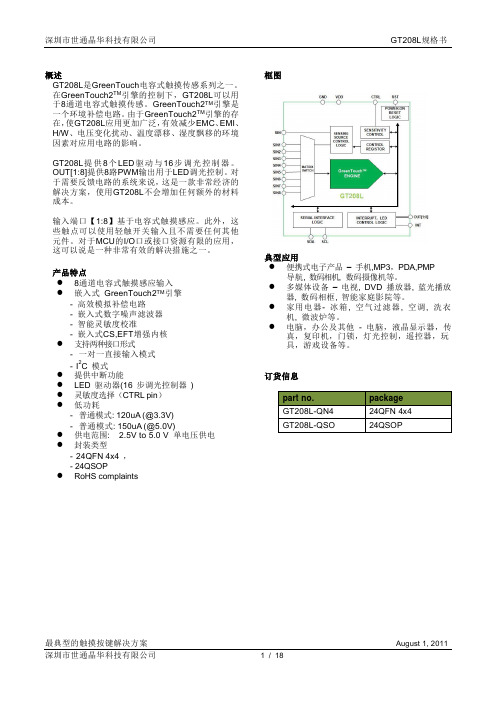
概述GT208L是GreenTouch电容式触摸传感系列之一。
在GreenTouch2TM引擎的控制下,GT208L可以用于8通道电容式触摸传感。
GreenTouch2TM引擎是一个环境补偿电路。
由于GreenTouch2TM引擎的存在,使GT208L应用更加广泛,有效减少EMC、EMI、H/W、电压变化扰动、温度漂移、湿度飘移的环境因素对应用电路的影响。
GT208L提供8个LED驱动与16步调光控制器。
OUT[1:8]提供8路PWM输出用于LED调光控制。
对于需要反馈电路的系统来说,这是一款非常经济的解决方案,使用GT208L不会增加任何额外的材料成本。
输入端口【1:8】基于电容式触摸感应。
此外,这些触点可以使用轻触开关输入且不需要任何其他元件。
对于MCU的I/O口或接口资源有限的应用,这可以说是一种非常有效的解决措施之一。
产品特点●8通道电容式触摸感应输入●嵌入式GreenTouch2TM引擎- 高效模拟补偿电路- 嵌入式数字噪声滤波器- 智能灵敏度校准- 嵌入式CS,EFT增强内核●支持两种接口形式- 一对一直接输入模式- I2C 模式●提供中断功能●LED 驱动器(16 步调光控制器)●灵敏度选择(CTRL pin)●低功耗- 普通模式: 120uA (@3.3V)- 普通模式: 150uA (@5.0V)●供电范围: 2.5V to 5.0 V 单电压供电●封装类型- 24QFN 4x4 ,- 24QSOP●RoHS complaints 框图典型应用●便携式电子产品–手机,MP3,PDA,PMP导航, 数码相机, 数码摄像机等。
●多媒体设备–电视, DVD 播放器, 蓝光播放器, 数码相框, 智能家庭影院等。
●家用电器- 冰箱, 空气过滤器, 空调, 洗衣机, 微波炉等。
●电脑,办公及其他- 电脑,液晶显示器,传真,复印机,门锁,灯光控制,遥控器,玩具,游戏设备等。
订货信息part no. packageGT208L-QN4 24QFN 4x4GT208L-QSO 24QSOP第一章:管脚说明1.1 24UQFN编号I/O 名称描述1 AI SIN4 通道4的感应电容或者轻触开关输入2 AI SIN5 通道5的感应电容或者轻触开关输入3 AI SIN6 通道6的感应电容或者轻触开关输入4 AI SIN7 通道7的感应电容或者轻触开关输入5 AI SIN8 通道8的感应电容或者轻触开关输入6 DO OLDO 控制外部LDO7 DI SCL I2C时钟端8 DIO SDA I2C数据端9 GND GND 接地10 PWR VPP 为MTP编程模式供电11 DI RST 复位12 DO OUT1 通道1PWM调光控制或者1对1直接输出13 DO OUT2 通道2PWM调光控制或者1对1直接输出14 DO OUT3 通道3PWM调光控制或者1对1直接输出15 DO OUT4 通道4PWM调光控制或者1对1直接输出16 DO OUT5 通道5PWM调光控制或者1对1直接输出17 DO OUT6 通道6PWM调光控制或者1对1直接输出18 DO OUT7 通道7PWM调光控制或者1对1直接输出19 DO OUT8 通道8PWM调光控制或者1对1直接输出20 DO INT 外部中断21 PWR VDD 电源22 AI SIN1 通道1的感应电容或者轻触开关输入23 AI SIN2 通道2的感应电容或者轻触开关输入24 AI SIN3 通道3的感应电容或者轻触开关输入*DI:数字信号输入,DO:数字信号输出,DIO:数字信号输入或输出,AI:模拟信号输入,AO:模拟信号输出,PWR:电源参考chapter 6 封装说明1.2 24QSOP编号I/O 名称描述1 AI SIN1 通道1的感应电容或者轻触开关输入2 AI SIN2 通道1的感应电容或者轻触开关输入3 AI SIN3 通道1的感应电容或者轻触开关输入4 AI SIN4 通道1的感应电容或者轻触开关输入5 AI SIN5 通道1的感应电容或者轻触开关输入6 AI SIN6 通道1的感应电容或者轻触开关输入7 AI SIN7 通道1的感应电容或者轻触开关输入8 AI SIN8 通道1的感应电容或者轻触开关输入9 DO OLDO 控制外部LDO10 DI SCL I2C时钟端11 DIO SDA I2C数据端12 GND GND 接地13 PWR VPP MTP编程模式供电14 DI RST 复位15 DO OUT1 通道1PWM调光控制或者1对1直接输出16 DO OUT2 通道2PWM调光控制或者1对1直接输出17 DO OUT3 通道3PWM调光控制或者1对1直接输出18 DO OUT4 通道4PWM调光控制或者1对1直接输出19 DO OUT5 通道5PWM调光控制或者1对1直接输出20 DO OUT6 通道6PWM调光控制或者1对1直接输出21 DO OUT7 通道7PWM调光控制或者1对1直接输出22 DO OUT8 通道8PWM调光控制或者1对1直接输出23 DO INT 外部中断24 PWR VDD 电源*DI:数字信号输入,DO:数字信号输出,DIO:数字信号输入或输出,AI:模拟信号输入,AO:模拟信号输出,PWR:电源参考chapter 6 封装说明第二章:电气特性(2)因为芯片内部有复位电路,外部复位不是必须的。
华擎 A770DE 主板 说明书
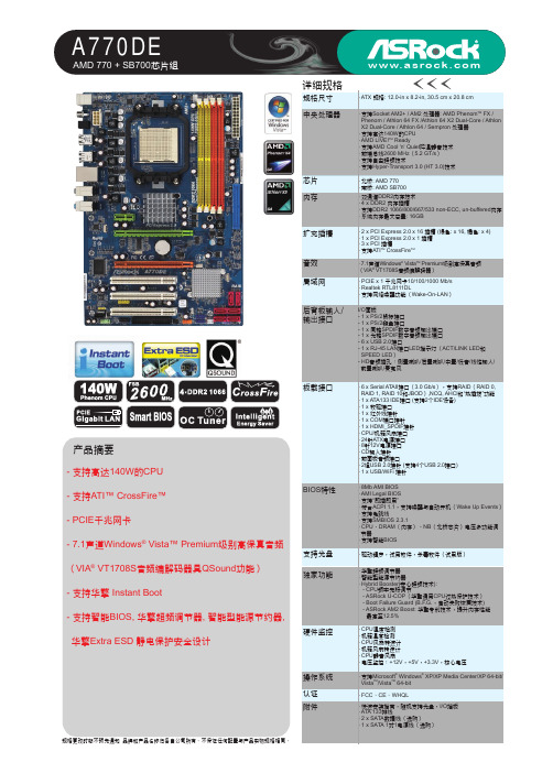
- CPU溫度檢測 - 机箱溫度檢測 - CPU風扇轉速計 - 机箱風扇轉速計 - CPU靜音風扇 - 電壓監控:+12V,+5V,+3.3V,核心電壓
- 支持Microsoft® Windows® XP/XP Media Center/XP 64-bit/ VistaTM/VistaTM 64-bit
從這個總結表中,我們可以發現華擎即時開机(ASRock Instant Boot)功能不僅在開机速度方面表現优异(3~4秒), 它還提供數据安全保障、保持操作系統的整洁,并且更節能。
- 支持高達140W的CPU - AMD LIVE!TM Ready - 支持AMD Cool 'n' Quiet降溫靜音技術 - 前端總線2600 MHz(5.2 GT/s) - 支持自由超頻技術 - 支持Hyper-Transport 3.0 (HT 3.0)技術
- 北橋: AMD 770 - 南橋: AMD SB700 - 雙通道DDR2內存技術 - 4 x DDR2 內存插槽 - 支持DDR2 1066/800/667/533 non-ECC, un-buffered內存 - 系統內存最大容量: 16GB
- 驅動程序,試用軟件,殺毒軟件(試用版)
- 華擎超頻調節器 - 智能型能源節約器 - Hybrid Booster(安心超頻技術):
- CPU頻率無段調節 - ASRock U-COP(華擎通用CPU過熱保護技術) - Boot Failure Guard (B.F.G.,啟動失敗恢复技術) - ASRock AM2 Boost: 華擎專利技術,提升內存性能
A770DE
AMD 770 + SB700芯片組
詳細規格
迪文科技DMG72720T041_06WTC屏幕数据手册说明书

DMT32240C028_06WTC2.8英寸240×320图形点阵65K色DGUS屏(DGUS II)2.8Inches,320xRGBx240,65K Colors,DGUS LCM(DGUS II)修订记录/Record of Revisio日期/Revise Date描述/Content2018-11-10首次发布/First Edition2020-08-25更新实物图/Update physical drawing●参数/Item数据/Parameter说明/Description颜色Color 65K(65536)色65K(65536)colors16bit调色板5R6G5B16bit color5R6G5B显示尺寸(A.A.)Active Area(A.A.)57.6mm(宽)×43.2mm(高)57.6mm(W)×43.2mm(H)240×320像素模式240*320分辨率Resolution 240×320像素240*320可设置成0°/90°/180°/270°显示模式Support0°/90°/180°/270°rotated displaySupport0°/90°/180°/270°rotated display背光模式Brightness LED 不低于10000H(以最高亮度连续工作,亮度减半时间)≥10000H(Continuous working with maximum brightness,time of brightness halves)亮度Brightness300nit 可进行100级亮度调节(当亮度调节至最高亮度的1%~30%时,可能出现闪烁现象,不建议在此范围使用)100levels adjustment(It's not recommend to set brightness to 1%~30%of the maximum,which may lead a flicker)注:超过30分钟长时间显示高对比度静止画面可能导致显示残影,请增加屏保避免该问题.Notice:Displaying a high contrast still screen for more than30minutes may result in an image blurring.Please add the screensaver to avoid.●电性能参数/Voltage&Current参数/Item测试条件/Conditions最小值/Min典型值/Typ 最大值/Max单位/Unit工作电压Power Voltage- 4.5 5.0 5.5V工作电流(不接扬声器时)Operation Current (None Speaker)VCC=+5V,背光亮度最大VCC=+5V,Backlight on-220-mA VCC=+5V,背光关闭VCC=+5V,Backlight off-80-mA推荐工作电源:5V1A的直流稳压电源Recommended power supply:5V1A DC ●工作环境和可靠性参数/Reliability Test参数/Item测试环境/Conditions最小值/Min典型值/Typ 最大值/Max单位/Unit工作温度Working Temperature 5V电压下,湿度60%60%RH at5V voltage-202570℃储存温度StorageTemperature--302585℃工作湿度Working Humidity25℃10%60%90%RH三防处理Protective Paint--无/None--出厂前老化时间Aging Test--无/None-H ●接口性能参数/Reliability Test参数/Item测试条件/Conditions最小值/Min典型值/Typ 最大值/Max单位/Unit串口波特率Baudrate 用户自定义(硬件配置文件设置)User set78411152007833600bps串口输出电平(TXD)Output Voltage (TXD)输出1,Iout=1mAOutput1,Iout=1mA3.0 3.3-V 输出0,Iout=-1mAOutput0,Iout=-1mA-00.3V串口输入电平(RXD)Input Voltage (RXD)输入1,Iin=1mAInput1,Iin=1mA2.43.3 5.0V 输入0,Iin=-1mAInput0,Iin=-1mA0-0.5V串口模式Interface UART2:N81,3.3V TTL/CMOSUART4:N81/E81/O81/N82四种模式可选,3.3V TTL/CMOS UART2:N81,3.3V TTL/CMOSUART4:Optional N81/E81/O81/N82mode,3.3V TTL/CMOS用户接口方式Socket10Pin_1.0mm FCCSD卡接口SD Slot 有(FAT32文件格式,SDHC)Yes(FAT32file format,SDHC)扬声器接口Speaker 2PIN_2.0mm 2Pin_2.0mm●存储器类别/Item参数/Parameter最小值/Min典型值/Typ 最大值/Max单位/UnitFLASH存储器Flash 字库储存空间Space of Font--64Mbytes 注:64MB字库空间后面32Mbytes为字库和音乐空间复用Font and audio file share the back half(32Mbytes)of Font Space.全屏图片储存数量Picture Storage--245幅/PcsRAM存储器RAM 变量存储空间Variable Storage Space-128-KbytesNor Flash用户数据库User database-320-Kbytes ●UI&外设支持/UI&PeripheralsUI和外设/UI&PeripheralUI版本UI VersionT5UID1支持外设Peripherals 电容式触摸屏,扬声器Capacitive touch panel,Speaker●包装和物理尺寸/Packing Capacity&Dimension尺寸/Dimension外形尺寸Dimension 85.2(宽)×55.6(高)×12.0(厚)mm 85.2(W)×55.6(H)×12.0(T)mm净重量Net Weight44g 包装标准/Packing Capacity包装箱型号Model 包装箱尺寸Size层数(层)Layer数量/层(片)Quantity/Layer总数量(片)Quantity(Pcs)1号箱/Carton1:220mm(L)×160mm(W)×47mm(H)1222号箱/Carton2:250mm(L)×200mm(W)×80mm(H)2243号箱/Carton3:320mm(L)×270mm(W)×80mm(H)2484号箱/Carton4:450mm(L)×350mm(W)×300mm(H)225505号箱/Carton5:600mm(L)×450mm(W)×300mm(H)260120备注:不影响性能参数和使用的产品设计变更,恕不另行通知。
迪文科技DMG80480C070_04WTC数据手册说明书

DMG80480C070_04WTC产品特点:●基于T5L0芯片,运行DGUS II系统,商业级产品。
●7.0寸,800*480分辨率,262K色,TV-TN屏。
●电容触摸屏。
Features:●Based on T5L0,running DGUS II system,commercial grade.●7.0-inch,800*480pixels resolution,262K colors,TV-TN-TFT-LCD.●Capacitive touch screen.硬件及接口Hardware and interface1.1硬件接口图Hardware interface硬件接口图Hardware interface1.2接口说明Interface description序号No.名称Name说明Description1T5L0芯片T5L0ASICT5L0芯片迪文自主研发,2020年量产,1MBytes片内Nor Flash,其中512KBytes用于存储用户数据库,擦写次数>100,000次T5L0ASIC Developed by DWIN.Mass production in2019,1MBytes NorFlash on the chip,512KBytes used to store the user database.Rewritecycle:over100,000times2液晶屏接口LCM interfaceFPC50_0.5mm,RGB接口FPC50_0.5mm,RGB interface3电容触摸屏接口CTP interfaceCOB结构,IIC接口COB structure,IIC interface4用户接口User interface用于供电和串口通讯,10Pin_1.0mm座子。
串口下载速率(典型值):12KByte/s10Pin_1.0mm socket for power supply and serial communication.Download rate(typical value):12KByte/s5Flash 16MBytes NOR Flash,存放字库、图片、音乐文件,擦写次数>100,000次16MBytes NOR Flash,for fonts,pictures and audio files.Rewrite cycle:over100,000times6蜂鸣器Buzzer3V无源蜂鸣器,功率:<1W3V passive buzzer.Power:<1W7SD卡接口SD interfaceFAT32格式,下载文件,文件可在屏幕统计显示,下载速率:4Mb/sFAT32.Download files by SD interface can be displayed in statistics.Download rate:4Mb/s8PGT05接口PGT05interface当产品因意外无法正常运行时,可通过PGT05更新DGUS底层,使产品重新恢复正常When product crashes by accident,you can use PGT05to update DGUSkernel and make the product return to normal2、规格参数Specification parameters 2.1显示参数Display parameters显示屏类型LCD TypeTV-TN,TFT LCD视角Viewing Angle TV视角,典型值70°/70°/40°/30°(L/R/U/D)TV viewing angle,70°/70°/40°/30°(L/R/U/D)分辨率Resolution 800×480(支持0°/90°/180°/270°显示模式)800×480pixels(support0°/90°/180°/270°)色彩Color 18位6R6G6B 18-bit6R6G6BAA区Active Area(A.A.)154.08mm(W)×85.92mm(H) VA区View Area(V.A.)-背光模式Backlight ModeLED背光寿命Backlight Service Life >20000小时(以最高亮度连续工作,亮度减半时间)>20000hours(Time of the brightness decaying to50%on the condition of continuous working with the maximum brightness)背光亮度Brightness170nit背光调节Brightness Control 100级亮度调节(当亮度调节至最高亮度的1%~30%时,可能出现闪烁现象,不背光调节建议在此范围使用)0~100grade(When the brightness is adjusted to1%~30%of the maximum brightness,flickering may occur and is not recommended to use in this range)注:超过30分钟长时间显示高对比度静止画面可能导致显示残影,请增加屏保避免该问题。
DE2_70开发板中文翻译
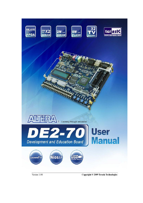
目录第1章DE2-70开发包 (1)1.1开发包内容 (1)1.2 DE2-70开发板的套件 (2)1.3 帮助 (3)第2章Altera DE2-70 开发板 (4)2.1 设计和组成 (4)2.2 DE2-70开发板结构框图 (5)2.3 驱动DE2-70开发板 (9)第3章DE2-70控制面板 (11)3.1 控制面板安装 (11)3.2控制LED、7段数码管和LCD显示器 (13)3.3开关和按键 (15)3.4 SDRAM/SSRAM/Flash控制器和编程器 (16)3.5 USB监视 (18)3.6 PS2设备 (19)3.7 SD卡 (20)3.8音频录放 (21)3.9 DE2-70控制面板的整个结构 (23)第4章DE2-70开发板视频功能 (25)4.1 视频功能的安装 (25)4.2 VGA显示 (26)4.3 视频抓取 (27)4.4 DE2_70开发板视频功能的整体结构 (28)第5章使用DE2-70开发板 (30)5.1配置Cyclone2 FPGA (30)5.2使用LED和SWITCH (32)5.3使用七段数码管 (36)5.4时钟电路 (38)5.5使用LCD模块 (40)5.6使用扩展槽 (41)5.7 VGA使用 (45)5.8 24位音频编解码芯片的使用 (48)5.9 RS_232串口 (49)5.10 PS/2串口 (49)5.11快速以太网控制器 (50)5.12视频解码器 (52)5.13视频编码器的实现 (54)5.14 USB主机和设备的使用 (55)5.15 IrDA的使用 (57)5.16 SDRAM/SRAM/Flash的使用 (58)第6章高级范例 (66)6.1 DE2-70出厂配置 (66)6.2 QuartusⅡ9.1和NiosⅡEDS9.1用户 (67)6.3 电视接收器示例 (67)6.4电视接收器画中画(PIP)示例...................................................................... (70)6.5 USB画笔 (73)6.6 USB设备 (75)6.7 卡拉OK机 (77)6.8 以太网数据包的发送与接收 (79)6.9 SD卡音乐播放器 (81)6.10 音乐合成器示例 (84)6.11 音频的录放 (88)第7章附录 (91)7.1 版本历史 (91)7.2 版权声明 (91)第1章DE2-70开发包DE2-70开发包包含了用于DE2-70开发板的全部组件以及在Microsoft Windows上运行的软件。
金山云AIoT智慧人居产品技术参数

-
产品名称:门磁 工作电压:3V电池(2节AAA 1.5伏碱性电池) 静态电流: <7uA 报警电流: <20mA 工作频率: 868.4 MHz ‒ 中国/欧洲 908.4 MHz ‒ 美国
921.4 MHz ‒ 澳洲 869.2 MHz ‒ 俄罗斯 发射距离:室内直线距离30米 室外直线距离50米 工作温度: -10℃〜+50℃ 相对湿度 ≤95%RH 外型尺寸:36x78x19 mm (⻔磁主体组件)
-
产品名称:天燃气报警器 产品尺寸:80*29mm(含安装板) 连接方式:zigbee 工作湿度:≤93% RH 工作温度:-10℃——+50℃ 供电方式:电源适配器 220V 0.2A 产品功能:天然气(甲烷)浓度检测、远程报警、
联动排⻛、定期自检提醒
-
产品名称:Aqara⻔窗传感器 连接方式:zigbee 产品尺寸:41*22*11mm 工作温度:-10℃−+50℃ 电池型号:CR1632 安装方式:玲珑小巧,即贴即用 产品功能:⻔窗状态监控和推送、有人闯入报警推送
-
产品名称:开关面板GTRV9A(G系列) 表面材质:不锈钢; 按键类别:锌合金包边系列开关; 产品尺寸:86*86mm,配宽边框92*92mm; 模块颜色:香槟金、黑色、土豪金、灰色; 连 体 位 :一位单体、两位连体、三位连体、四位连体;
-
产品名称:产品系列:GTRD8B(D系列) 表面材质:不锈钢; 表面处理: 磨砂/拉丝; 按键类别:金属大板全包边轻触开关; 产品尺寸: 86*86mm,配宽边框92*92mm; 模块颜色:高级灰、高级黑、高级白、枪色; 连 体 位 :一位单体、两位连体、三位连体、四位连体;
-
产品名称:Aqara墙壁开关D1(零火版) 连接方式:Zigbee 负载范围:Max2200W 产品尺寸:86*86*42.8mm 款式选择:D1系列单键版、双键版、三键版 安装要求:86底盒内需预留零线 产品功能:远程控制、语音控制、智能联动、过载保护、
- 1、下载文档前请自行甄别文档内容的完整性,平台不提供额外的编辑、内容补充、找答案等附加服务。
- 2、"仅部分预览"的文档,不可在线预览部分如存在完整性等问题,可反馈申请退款(可完整预览的文档不适用该条件!)。
- 3、如文档侵犯您的权益,请联系客服反馈,我们会尽快为您处理(人工客服工作时间:9:00-18:30)。
Page 2 of 4
2004 Jun 01
Document Revision Level A
元器件交易网
Product Specification
D8740270GT
GaAs Power Doubler, 40 – 870MHz, 27.0dB min. Gain @ 870MHz, 375mA max. @ 24VDC
max 44,8 13,8 20,9 8,15 12,75 38,3 4,2 4,2 25,6
4,4 27,4 12,1 6,2 0,27 0,48 2,84 3,04 2,79 5,33 5,33
Page 3 of 4
2004 Jun 01
Document Revision Level A
元器件交易网
f = 40 to 320 MHz f = 320 to 640 MHz f = 640 to 870 MHz
f = 40 to 320 MHz f = 320 to 640 MHz f = 640 to 870 MHz f = 50 to 870 MHz
MIN.
27.0 0.5
-
TYP.
1.0
20.0 19.0 17.0 20.0 19.0 18.0
Cross Modulation (XMOD) Cross modulation (XMOD) is measured at baseband (selective voltmeter method), referenced to 100% modulation of the carrier being tested.
input return loss
S22
output return loss
F
noise figure
Itot
total current
consumption (DC)
CONDITIONS
f = 870 MHz f = 40 to 870 MHz f = 40 to 870 MHz
(Peak to Valley)
பைடு நூலகம்
This data sheet contains target or goal specifications for product development. This data sheet contains preliminary data; supplementary data may be published later. This data sheet contains final product specifications.
SYMBOL
Vi Vov Tstg Tmb
PARAMETER
RF input voltage (single tone) DC supply over-voltage (5 minutes) storage temperature operating mounting base temperature
MIN.
-
TYP.
MAX.
- 60 - 55 - 63
UNIT
dBc dBc dBc
Notes: 1) 112 channels, NTSC frequency raster: 55.25 MHz to 745.25 MHz, +40 dBmV to +50 dBmV tilted output level.
A
44,6 ± 0,2
B
13,6 ± 0,2
C
20,4 ± 0,5
D
8 ± 0,15
E
12,6 ± 0,15
F
38,1 ± 0,2
G
4 +0,2 / -0,05
H
4 ± 0,2
I
25,4 ± 0,2
J
UNC 6-32
K
4,2 ± 0,2
L
27,2 ± 0,2
M
11,6 ± 0,5
N
5,8 ± 0,4
D8740270GT
GaAs Power Doubler Hybrid
40 – 870MHz 27.0dB min. Gain @ 870MHz
375mA max. @ 24VDC
MIN.
- 40 - 30
MAX.
75 30 + 100 + 100
UNIT
dBmV V °C °C
CHARACTERISTICS
Table 1: S-Parameter, Noise Figure, DC Current; VB = 24V; Tmb = 30°C; ZS = ZL = 75 Ω
SYMBOL
Gp SL FL
S11
PARAMETER
power gain slope 1)
flatness of frequency response
O
0,25 ± 0,02
P
0,45 ± 0,03
Q
2,54 ± 0,3
R
2,54 ± 0,5
S
2,54 ± 0,25
T
5,08 ± 0,25
U
5,08 ± 0,25
min 44,4 13,4 19,9 7,85 12,45 37,9 3,95 3,8 25,2
4,0 27,0 11,1 5,4 0,23 0,42 2,24 2,04 2,29 4,83 4,83
350.0
MAX.
28.2 1.5 0.6
5.0 375.0
UNIT
dB dB dB
dB dB dB dB dB dB dB mA
Notes: 1) The slope is defined as the difference between the gain at the start frequency and the gain at the stop frequency.
Page 1 of 4
2004 Jun 01
Document Revision Level A
元器件交易网
Product Specification
D8740270GT
GaAs Power Doubler, 40 – 870MHz, 27.0dB min. Gain @ 870MHz, 375mA max. @ 24VDC
I U
123 5 789 C
E
M
R
J
S
P
K
O
T
øG
Q
N
D H
B
INPUT GND GND +VB GND GND OUTPUT
L F A
0 5 10mm scale
Pinning:
1 2 34567 8 9
Notes:
European Projection
All Dimensions in mm:
nominal
APPLICATION
• 40 to 870 MHz CATV amplifier systems
DESCRIPTION
• Hybrid Power Doubler amplifier module employing GaAs dice
LIMITING VALUES
In accordance with the Absolute Maximum Rating System (IEC 60134)
Application information
Where application information is given, it is advisory and does not form part of the specification.
Premier Devices reserves the right to make changes without further notice to any products herein. Premier Devices makes no warranty representation or guarantee regarding the suitability of its products for any particular purpose, nor does Premier Devices assume any liability arising out of the application or use of any product or circuit, and specifically disclaims any and all liability, including without limitation consequential or incidental damages. “Typical” parameters which may be provided in Premier Devices datasheets and/or specifications can and do vary in different applications and actual performance may vary over time. All operating parameters, including “Typicals” must be validated for each customer application by customer´s technical experts. Premier Devices does not convey any license under its patent rights nor the rights of others. Premier Devices products are not designed, intended, or authorized for use as components in systems intended for surgical implant into the body, or other applications intended to support or sustain life, or for any other application in which the failure of the Premier Devices product could create a situation where personal injury or death may occur. Should Buyer purchase or use Premier Devices products for any such unintended or unauthorized application, Buyer shall indemnify and hold Premier Devices and its officers, employees, subsidiaries, affiliates, and distributors harmless against all claims, costs, damages, and expenses, and reasonable attorney fees arising out of, directly or indirectly, and claim of personal injury or death associated with such unintended or unauthorized use, even if such claim alleges that Premier Devices was negligent regarding the design or manufacture of the part.