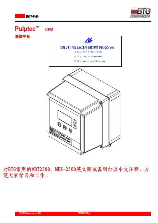
BTR-3580G中文资料
产品培训资料2013325

1
27MHz晶体
5×5 mm QFN40
27MHz
27MHz
5.2dB
5.5dB
-7dB
-10dB
11
除上表格列出的参数外Tuner的参数还包括 输入三阶截止点(IIP3),输入二阶截止点 (IIP2), IQ 振幅平衡 (IQAB ),IQ 相位平衡 (IQPB),相位噪声 (PN),等!详细参数 请参阅产品规格书。
AGC范围(dB)
80
85
86
80
频道带宽(MHz) 4-40
4-40
4-40
4-40
供给电压(V)
2.97-3.63 3-3.6
2.97-3.63
3-3.6
功耗
小于 500mW
小于600mW
小于500mW
---
封装
3*3mm QFN28
4×4mm QFN24
4×4mm QFN28
4×4 mm QFN24
输入反射系 -5dB
-7dB
RDA5815M (新)
0.9-2.2GHz
RDA5816S(双头)(新)
0.9-2.2GHz
-100 to 5dBm -100 to 0dBm
85dB
80dB
4MHz-40MHz 4MHz-40MHz
3V-3.6V
3V-3.6V
小于500mW
---
max3485中文资料

max3485中文资料max3485eesa + T概述Max3485eesa + T是3.3V电源±15kV ESD保护,真正的RS485 / RS422收发器,采用8引脚nsoic封装。
该低功耗收发器包含一个驱动器和一个接收器。
max3485e传输速率高达15Mbps。
它具有增强的静电保护。
所有发送器输出和接收器输入均具有±15kV保护,并通过IEC 1000-4-2气隙放电;±8Kv保护是通过IEC 1000-4-2接触放电,±15kV保护是通过人体模型。
驱动器受到短路电流的限制,并通过将驱动器输出置于高阻抗状态的热关断电路来防止过多的功耗。
接收器输入具有故障安全功能,如果两个输入均打开,则提供逻辑高电平输出。
Max3485e适用于EMI敏感应用,集成服务,数字网络和数据包交换电源电压范围:3V至3.6V工作温度范围-40°C至85°C半双工通讯该操作由单个+ 3.3V电源供电,无电荷泵兼容+ 5V逻辑2Na小电流关闭模式共模输入电压范围:-7V至+ 12V工业标准75176引脚输出驱动器/接收器启用功能工业控制LAN,ISDN,低功耗RS-485 / RS-422收发器;分组交换;电信;用于EMI敏感应用的收发器Max3483,max3485,max3486,max3488,max3490和max3491是用于RS-485和RS-422通信的3.3V低功耗收发器,每个收发器都有一个驱动器和一个接收器。
Max3483和max3488具有有限速率驱动器,可以降低EMI并减少由于端子匹配电缆不合适而引起的反射,从而实现高达250kbps的无错误数据传输。
由于其有限的摆幅速率,Max3486可以实现最大2.5mbps 的传输速率。
Max3485,max3490和max3491可以实现高达10Mbps的传输速率。
驱动器具有短路电流限制,并且可以通过热关断电路将驱动器的输出设置为高阻状态,以防止过多的功率损耗。
BT152中文资料

BT152中⽂资料GENERAL DESCRIPTIONQUICK REFERENCE DATAGlass passivated thyristors in a plastic SYMBOL PARAMETERMAX.MAX.MAX.UNIT envelope,intended for use in applications requiring high BT152-400R 600R 800R bidirectional blocking voltage V DRM ,Repetitive peak off-state 450650800V capability and high thermal cycling V RRM voltages performance.Typical applications I T(AV)Average on-state current 131313A include motor control,industrial and IT(RMS)RMS on-state current202020A domestic lighting,heating and static I TSMNon-repetitive peak on-state 200200200Aswitching.currentPINNING - TO220ABPIN CONFIGURATIONSYMBOLLIMITING VALUESLimiting values in accordance with the Absolute Maximum System (IEC 134).SYMBOL PARAMETERCONDITIONSMIN.MAX.UNIT -400R -600R -800R V DRM Repetitive peak off-state -45016501800V voltagesI T(AV)Average on-state current half sine wave; T mb ≤ 103 ?C -13A I T(RMS)RMS on-state current all conduction angles-20A I TSMNon-repetitive peak half sine wave; T j = 25 ?C prior to on-state currentsurge t = 10 ms -200A t = 8.3 ms -220A I 2t I 2t for fusingt = 10 ms-200A 2s dI T /dt Repetitive rate of rise of I TM = 50 A; I G = 0.2 A;-200A/µs on-state current after dI G /dt = 0.2 A/µs triggering I GM Peak gate current -5A V GM Peak gate voltage-5V V RGM Peak reverse gate voltage -5V P GM Peak gate power -20W P G(AV)Average gate power over any 20 ms period -0.5W T stg Storage temperature -40150?C T jOperating junction -125Ctemperature1 Although not recommended, off-state voltages up to 800V may be applied without damage, but the thyristor may switch to the on-state. The rate of rise of current should not exceed 15 A/µs.THERMAL RESISTANCESSYMBOL PARAMETERCONDITIONSMIN.TYP.MAX.UNIT R th j-mb Thermal resistance-- 1.1K/W junction to mounting base R th j-aThermal resistance in free air -60-K/Wjunction to ambientSTATIC CHARACTERISTICST j = 25 ?C unless otherwise stated SYMBOL PARAMETER CONDITIONSMIN.TYP.MAX.UNIT I GT Gate trigger current V D = 12 V; I T = 0.1 A -332mA I L Latching current V D = 12 V; I GT = 0.1 A -2580mA I H Holding current V D = 12 V; I GT = 0.1 A -1560mA V T On-state voltage I T = 40 A- 1.4 1.75V V GT Gate trigger voltage V D = 12 V; I T = 0.1 A-0.6 1.5V V D = V DRM(max); I T = 0.1 A; T j = 125 ?C 0.250.4-V I D , I ROff-state leakage currentV D = V DRM(max); V R = V RRM(max); T j = 125 ?C-0.21.0mADYNAMIC CHARACTERISTICST j = 25 ?C unless otherwise stated SYMBOL PARAMETER CONDITIONSMIN.TYP.MAX.UNIT dV D /dt Critical rate of rise of V DM = 67% V DRM(max); T j = 125 ?C;200300-V/µs off-state voltageexponential waveform gate open circuit t gt Gate controlled turn-on V D = V DRM(max); I G = 0.1 A; dI G /dt = 5 A/µs;-2-µs timeI TM = 40 At qCircuit commutated V D = 67% V DRM(max); T j = 125 ?C;-70-µsturn-off timeI TM = 50 A; V R = 25 V; dI TM /dt = 30 A/µs;dV D /dt = 50 V/µs; R GK = 100 ?MECHANICAL DATANotes1. Refer to mounting instructions for TO220 envelopes.2. Epoxy meets UL94 V0 at 1/8".DEFINITIONSData sheet statusObjective specification This data sheet contains target or goal specifications for product development. Preliminary specification This data sheet contains preliminary data; supplementary data may be published later. Product specification This data sheet contains final product specifications.Limiting valuesLimiting values are given in accordance with the Absolute Maximum Rating System (IEC 134). Stress above one or more of the limiting values may cause permanent damage to the device. These are stress ratings only and operation of the device at these or at any other conditions above those given in the Characteristics sections of this specification is not implied. Exposure to limiting values for extended periods may affect device reliability. Application informationWhere application information is given, it is advisory and does not form part of the specification.Philips Electronics N.V. 1997All rights are reserved. Reproduction in whole or in part is prohibited without the prior written consent of the copyright owner.The information presented in this document does not form part of any quotation or contract, it is believed to be accurate and reliable and may be changed without notice. No liability will be accepted by the publisher for any consequence of its use. Publication thereof does not convey nor imply any license under patent or other industrial or intellectual property rights.LIFE SUPPORT APPLICATIONSThese products are not designed for use in life support appliances, devices or systems where malfunction of these products can be reasonably expected to result in personal injury. Philips customers using or selling these products for use in such applications do so at their own risk and agree to fully indemnify Philips for any damages resulting from such improper use or sale.。
用户手册

CS5340-CZZR中文资料

Single-Ended Analog Input
AINR Switch-Cap ADC
High-Pass Filter
Low-Latency Digital Filters
Serial Port
VL 1.8 V to 5 V
Auto-detect MCLK Divider
Master Clock
Slave Mode Auto-detect
2. PIN DESCRIPTION .............................................................................................................................. 13 3. TYPICAL CONNECTION DIAGRAM ................................................................................................... 14 4. APPLICATIONS ................................................................................................................................... 15
192 kHz 101 dB Dynamic Range at 5 V -94 dB THD+N 90 mW Power Consumption High-Pass Filter to Remove DC Offsets Analog/Digital Core Supplies from 3.3 V to 5 V Supports Logic Levels between 1.8 V and 5 V Auto-detect Mode Selection in Slave Mode Auto-Detect MCLK Divider Pin Compatible with CS5341
BTG2500中英文使用说明书
ISA-358G备自投产品手册

ISA-358G备自投产品手册该产品手册介绍了ISA-358G备自投产品的特点、功能以及操作指南。
产品特点- ISA-358G备自投产品是一款高效、可靠的备份和恢复解决方案。
- 它具有强大的数据处理和存储能力,适用于各种规模的企业。
- 产品使用先进的技术和算法,保证数据的完整性和安全性。
产品功能- 数据备份:ISA-358G可以根据设定的计划自动备份重要数据。
可支持全量备份和增量备份,灵活满足企业需求。
- 数据恢复:在数据丢失或损坏的情况下,ISA-358G能够快速恢复丢失的数据,保证业务的连续性。
- 数据压缩和加密:产品支持数据的压缩和加密,减少存储空间需求同时保护数据的机密性。
- 定时计划:用户可以按照自己的需求设置备份计划,可以根据日、周、月来灵活选择备份频率。
- 监控和报告:ISA-358G提供实时监控和详细的备份报告,帮助用户及时了解备份状态和效果。
操作指南1. 首次使用:拆开产品包装,将ISA-358G主机和相应的连接线插入电源和网络接口。
2. 系统初始化:根据产品说明书中的提示,进行系统初始化和设置。
3. 参数配置:登录系统后,根据实际需求进行参数配置,如备份计划、数据压缩和加密等。
4. 数据备份:根据备份计划设置好的时间和频率,自动执行数据备份操作。
5. 数据恢复:在需要恢复数据时,通过系统界面选择相应备份点,并进行数据恢复操作。
6. 系统监控和维护:定期监控备份状态,及时处理异常情况。
定期维护系统,确保其正常运行。
请注意,以上只是产品手册的概要内容。
详细的操作步骤和注意事项,请参考附带的产品说明书。
有关更多信息或技术支持,请联系我们的客户服务部门。
感谢您选择ISA-358G备自投产品!。
MAX31855热电偶芯片的中文翻译
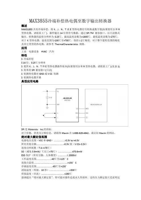
MAX3855冷端补偿热电偶至数字输出转换器概述MAX31855具有冷端补偿,将K、J、N、T或E型热电偶信号转换成数字量(如果使用S和R 型热电偶,请联系工厂)。
器件输出14位带符号数据,通过SPI TM 兼容接口、以只读格式输出。
转换器的温度分辨率为0.25℃,最高温度读数为+1800℃,最低温度读数为-270℃,对于K型热电偶,温度范围为-200℃至+700℃,保持±2℃精度。
对于整个量程范围的精度及其它类型的热电偶,请参考ThermalCharacteristics 规格。
应用工业电器设备HVAC 汽车特性S 冷端补偿S 14位、0.25℃分辨率S 提供K、J、N、T和E型热电偶器件版本(如果使用S和R型热电偶,请联系工厂) (见表1) S 简单的SPI兼容接口(只读)S 检测热电偶对GND或V CC 短路S 检测热电偶开路典型应用电路SPI是Motorola,Inc.的商标。
对于价格,供货及订购信息,请联络Maxim在1-888-629-4642,或访问Maxim的网站。
绝对最大额定值范围电源电压范围(VCC和GND)..................-0.3V to +4.0V所有其他引脚............................................-0.3V到(V CC+ 0.3V)连续功率耗散(T A =+70℃)SO(减免5.9mW/ ℃以上+70℃).......................470.6mWESD保护(所有引脚,人体模型).............±2000kV工作温度范围........................-40℃至+125°C连接点温度................................................ .....+150°C存储温度范围..........................-65℃至+150°清除温度(焊接,10秒) (300)焊接温度(回流) (260)强调超出“绝对最大额定值”,即可能对器件造成永久性损坏。
LT3580中文资料

SYNC Voltage............................................ –0.3V to 5.5V Operating Junction Temperature Range
LT3580E (Notes 2, 5) .........................–40°C to 125°C LT3580I (Notes 2, 5)..........................–40°C to 125°C Storage Temperature Range...................–65°C to 150°C
2
2.2
200 220
1/4
2500
mA μA %/V MHz kHz Ratio kHz
SYNC High Level for Synchronization
l 1.3
V
SYNC Low Level for Synchronization
VSHDN = 2.5V, Not Switching VSHDN = 0V 2.5V ≤ VIN ≤ 32V RT = 45.3k RT = 464k Compared to Normal fOSC SYNCing or Free Running
l 1.8 l 180
l 200
1
1.5
0
1
0.01 0.05
元器件交易网
LT3580
Boost/Inverting DC/DC Converter with 2A Switch, Soft-Start, and Synchronization
FEATURES
n 2A Internal Power Switch n Adjustable Switching Frequency n Single Feedback Resistor Sets VOUT n Synchronizable to External Clock n High Gain SHDN Pin Accepts Slowly Varying
北京新超仁达数据采集卡产品型录
配套端子板 ADAM-3937 P-500 P-800 P-510 P-512 PCLD-789D
DB-37 针孔型接口接线端子 带 1 个 40 针排线接插件和一个 37 针 D-sub 插针通用端子板 带 16 路继电器输出通用端子板 带 8 路隔离数字量输入端子板 带 8 路隔离数字量输出端子板 放大及多路选通板
概述 PCL-812PG 是为 IBM 或其他兼容计算机设计的一款高性能、高速多功能数据采集卡。
PCL-812PG 具备所有数据采集卡的功能,例如,A/D ,D/A 转换,DIO 和定时/计数器,本 卡的高规格使其在需要高速采集的情况下得到广泛应用。PCL-812PG 为低电平输入(例如, 热耦合信号测量)提供专门的高增益可编程仪表放大器。
订货信息 PCL-711B
8 路 12 位 50KS /s 高性价比多功能数据采集
新超控制
3/65
ISA 总线(多功能)
PC-1204 ISA 总线 AD,DA,DIO,脉冲计数/定时中断多功能综合板
特性: AD 输入通道:12 位 100KHz ,*单端 16 路/差分 8 路 AD 输入量程:单极性:0~5V,0~10V* 双极性:±2.5V,±5V,±10V 输入阻抗:>10MΩ;转换误差:<0.20% 输出码制:单极性为二进制原码 双极性为二进制偏移码 工作方式:软件查询、中断 最大差动输入值:20V 输出通道:12 位独立 4 路 输出信号范围: 电压方式:0~5V;0~10V*;±5V;±10V 电流方式:4~20mA 输出阻抗:≤2Ω D/A 转换码制:二进制原码(单极性) 二进制偏移码(双极性) D/A 转换时间:≤1μs D/A 转换综合误差: 电压方式:≤0.2﹪ FSR 电流方式:≤1﹪ FSR 电压输出方式负载能力:5mA/每路 16 路 TTL 电平开关量输入、输出 输出带锁存,输出电流≤2mA
BT200中文说明书
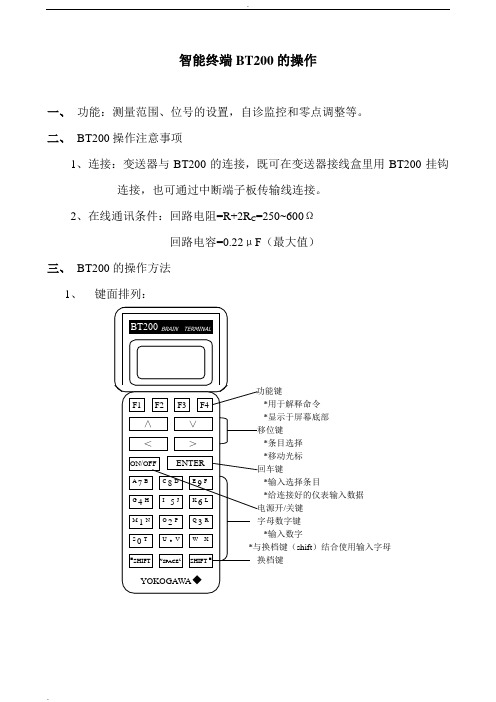
智能终端BT200的操作一、功能:测量范围、位号的设置,自诊监控和零点调整等。
二、BT200操作注意事项1、连接:变送器与BT200的连接,既可在变送器接线盒里用BT200挂钩连接,也可通过中断端子板传输线连接。
2、在线通讯条件:回路电阻=R+2R C=250~600Ω回路电容=0.22μF(最大值)三、BT200的操作方法1、键面排列:*用于解释命令*显示于屏幕底部*条目选择*移动光标*输入选择条目*给连接好的仪表输入数据/关键*输入数字shift)结合使用输入字母菜单页页主题种显示)参量 功能命令BT200键面图2、 操作键的功能⑴ 数字/字母键和利用数字/字母键直接输入数字,结合 a :输入数字、符号和空格(0—9…) 直接按数字/字母键b :输入字母(A —Z )选按下shift 键,再同时按数字/字母键,则输入数字/字母键上与shift 键边侧位置相对应的字母.注意在按数字/字母键前必须先按下shift 键。
数字/字母键 数字/字母键 上的左侧字母 上右侧字母 * 用功能键F2键,大小写字形作一次更换并锁定。
*使用功能键[F1]输入符号。
每按一下 1 。
- 、+ * )( ’ & % $ # ” !这些符号后面输入字母,要选按[>]移动光标。
*使用功能键[F1]输 ⑵ 功能键功能命令功能键功 能 命 令 表ON/OFF 3、用操作键调示菜单四、BT200的参数设置1、参数总表适用仪表:F:差压变送器……EJA110A,EJA120A,EJA118W,EJA118Y,EJA115 P:压力变送器……EJA310A,EJA430A,EJA438W,EJA438N,EJA530A L:液位变送器……EJA210A,EJA220A*1.EJA120不能检测静压,此处显示值为0kPa,但液值不是测量值。
*2.仪表最大工作压力在主铭牌上标明,B40是膜盒最大工作压力。
2、参数意义和选择※参数设置后30秒内关机,设定参数不被存储,最终值返回原值在讲述参数设置之前,先列表说明在各种情况下参数的意义。
雷达防砸车检器说明书

道闸雷达用户手册二O一九年五月目录一.产品简介 (1)二.产品规格 (2)三.技术特点 (4)四.安装调试 (6)五.使用注意事项 (13)一.产品简介道闸雷达是一种非接触式的针对车辆和行人等目标的检测装置,工作在毫米波频段,利用向目标发射线性调频连续波信号,对目标反射回波进行高速实时处理,实现目标的快速检测。
道闸雷达主要应用于园区、住宅小区、公司的车辆出入口、高速公路出入口以及停车场管理等,替代现有的地感线圈,控制闸杆降落功能,防止闸杆“砸车”,“砸人”事故发生。
道闸雷达的外形实物如图1所示。
图1 道闸雷达外形图道闸雷达具有安装维护方便、不需破坏路面、不影响车辆出入通行、技术先进、工作可靠稳定、成本低、作用距离可灵活设置、全天时和全天候工作、可兼容直杆和广告牌/栅栏闸杆应用等优点。
二.产品规格道闸雷达包括两种型号规格:RDDZ-001型, RDDZ-002型。
RDDZ-001型产品:1路开关量输出;RDDZ-002型产品:2路开关量输出,1路RS485/RS232总线。
1.技术指标中心频率:24 GHz;垂直方向波束宽度:43°;水平方向波束宽度:11°;覆盖距离范围:0.2 m~6 m;距离调节范围:2.0 m~6 m(8档);响应时间:100 ms;信号输出:开关量。
2.检测精度车辆检测漏检率:0.1%;行人检测漏检率:0.1%;误检率:0.05%。
3.机械特性设备尺寸:105 mm×78 mm×26 mm;重量:85 g;防水等级符合IP-65标准。
4.电源要求工作电压范围:DC 6V~18V;工作电流:小于90 mA/12V。
5.工作环境条件温度范围:-40℃~+85℃;湿度范围:25℃下相对湿度99%。
6.可靠性设备在规定条件下,可昼夜连续工作,其平均无故障间隔时间(MTBF)满足:MTBF≧15000 h。
三.技术特点1.全天时和全天候工作道闸雷达工作信号为毫米波频段,无需专门散热处理,在兩、雪、冰雹、雾霾等天气条件下,具备昼夜连续工作能力,产品外壳具备IP-65防水要求,无需担心雨水进入雷达内而导致雷达损坏问题。
森林资源调查仪林务通参数

6.遥感影像波段及透明设置;
7点导航、取点导航、属性导航,并且可以批量导入导航点;
8可以分别加载到arcgis与谷歌地图中进行查看具体的路线图;
9拍摄与矢量图有关联且带有坐标的照片,照片可以在地图界面直接进行预览和导航;
网络制式LTE-TDD:Band 38/39/40/41(100MHz),LTE-FDD:Band 1/3/5/7/8/19/20/28,TD-SCDMA:Band 34/39,WCDMA:Band 1/2/5/6/8/19,GSM:850/900/1800/1900MHz
数据业务LTE(最高下行150 Mbit/s /上行50Mbit/s),DC-HSDPA+(最高下行42 Mbit/s /上行5.76Mbit/s)
显卡芯片Mali-T880
显示屏
屏幕尺寸8.4英寸
屏幕分辨率2560x1600
屏幕像素密度359PPI
屏幕描述电容式触摸屏,多点式触摸屏
指取设备触摸屏
屏幕特性十点式触摸屏,IPS屏幕
网络通讯
网络类型移动4G(TD-LTE),联通4G(TD-LTE/LTE FDD),移动3G(TD-SCDMA),联通3G(WCDMA),移动2G/联通2G(GSM)
10实用的截屏标记功能,可方便地制作位置示意图;
11支持距离、面积、坐标查询功能和任意点查询功能;
12系统内部可将采集的数据按照类型进行分类管理,方便用户进行快捷查找,同时在导出时,可分别导出KMZ、GPX、SHP多种矢量格式;
13支持栅格数据无缝拼接;
3、支持数据在线地图与shp数据的叠加,在线地图包括卫星图、等高线图、道路图;参考GIS行业标准进行图层管理界面的设计,支持对图层的加载、显示、设置等操作;
BTR-3540G中文资料

Optoway BTR-3540G*********************************************************************************************************************************************************************************************************************************************************************************************************************************************OPTOWAY TECHNOLOGY INC. No .38, Kuang Fu S. Road, Hu Kou, Hsin Chu Industrial Park, Hsin Chu, Taiwan 303Tel: 886-3-5979798 Fax: 886-3-59797371BTR-3540G / BTR-3540-SPG / BTR-3540AG / BTR-3540A-SPG1550 nm TX / 1310 nm RX , 5V / 155 Mbps RoHS Compliant Single-Fiber Transceiver*********************************************************************************************************************************************************************FEATURESl Single Fiber Bi-Directional Transceiver l 1550 nm DFB LD Transmitter l 1310 nm Receiver l Distance Up to 40 kml Industry Standard 1 x 9 Footprint l Single +5 V Power Supply l RoHS Compliantl PECL Differential Inputs and Outputsl 0 to 70o C Operating Temperature: BTR-3540G l -20 to 85o C Operating Temperature: BTR-3540AG l Wave Solderable and Aqueous Washablel Class 1 Laser International Safety Standard IEC-60825 CompliantAPPLICATIONSl WDM 155 Mb/s Linksl SONET/SDH Equipment Interconnect l Fast Ethernet 100 Mb/s LinksDESCRIPTIONThe BTR-3540G series is high performance module for single fiber communications by using 1550 nm transmitter and 1310 nm receiver. The transmitter section uses a multiple quantum well DFB laser and is a class 1 laser compliant according to International Safety Standard IEC-60825. The receiver section uses an integrated 1310 nm detector preamplifier (IDP) mounted in an optical header and a limiting post-amplifier IC. A PECL logic interface simplifies interface to external circuitry.LASER SAFETYThis single mode transceiver is a Class 1 laser product. It complies with IEC-60825 and FDA 21 CFR 1040.10 and 1040.11. The transceiver must be operated within the specified temperature and voltage limits. The optical ports of the module shall be terminated with an optical connector or with a dust plug.ORDER INFORMATIONP/No.Bit Rate (Mb/s) Distance(km) TX (nm) RX (nm) Voltage (V) Package Temp (o C) TX Power (dBm) RX Sens. (dBm) RoHS Compliant BTR-3540G 125/155 40 1550 DFB 1310 5 1X9 0 to 70 -3 to -8 -33 Yes BTR-3540AG125/155401550 DFB131051X9-20 to 85-3 to -8 -33 YesNote: 1. BTR-XXXXXG is 1X9 SC receptacle type package.2. BTR-XXXXX-XPBBBG is 1X9 pigtail type package with different connector, A=S is SC connector, A=F is FCconnector, A=T is ST connector, A=L is LC connector, A=M is MU connector; BBB is the length of fiber in cm.Absolute Maximum RatingsParameterSymbol Min Max Units NotesStorage Temperature Tstg -40 85 o COperating Temperature Topr 0 -20 70 85 o CBTR-3540G BTR-3540AGSoldering Temperature --- 260 oC 10 seconds on leads only Power Supply Voltage Vcc 0 6 V Input Voltage --- GND Vcc VOutput CurrentIout30mARecommended Operating ConditionsParameterSymbol Min Typ Max Units Power Supply Voltage Vcc 4.75 5.00 5.25 V Operating Temperature Topr 0 -20 70 85 oC / BTR-3540G oC / TR-3540AGData Rate155 170 Mb/s Power Supply CurrentIcc280mA***********************************************************************************************************************************************************************OPTOWAY TECHNOLOGY INC. No .38, Kuang Fu S. Road, Hu Kou, Hsin Chu Industrial Park, Hsin Chu, Taiwan 303Tel: 886-3-5979798 Fax: 886-3-5979737Transmitter Specifications (0o C < Topr < 70o C, 4.75V < Vcc < 5.25V)ParameterSymbolMinTypMaxUnitsNotesOpticalOptical Transmit Power Po -8 --- -3 dBm 1Output Center Wavelength λ1480 1580 nm Output Spectrum Width ∆λ--- --- 1 nm -20 dB Width Extinction Ratio E R 10 --- --- dB Output EyeCompliant with Bellcore GR-253-CORE and ITU recommendation G.957Optical Rise Time t r 2 ns 10% to 90% Values Optical Fall Timet f 2 ns 10% to 90% Values Relative Intensity Noise RIN -116 dB/Hz Total Jitter TJ 1.0 ns 2 ElectricalData Input Current – Low I IL -350 µA Data Input Current – High I IH 350 µA Differential Input Voltage V IH - V IL 300 mVData Input Voltage – Low V IL - V CC -2.0 -1.58 V 3 Data Input Voltage -- HighV IH - V CC-1.1-0.74V3Notes: 1. Output power is power coupled into a 9/125 µm single mode fiber.2. Measured with a 223-1 PRBS with 72 ones and 72 zeros.3. These inputs are compatible with 10K, 10KH and 100K ECL and PECL inputs.Receiver Specifications (0o C < Topr < 70o C, 4.75 V < Vcc < 5.25V)ParameterSymbol Min Typ Max Units Notes Optical Sensitivity--- --- --- -33 dBm 1Maximum Input Power Pin -3 --- --- dBmSignal Detect -- Asserted Pa --- --- -33 dBm Transition: low to high Signal Detect -- Deasserted Pd -43 --- --- dBm Transition: high to low Signal detect -- Hysteresis 1.0 --- 4.0 dBWavelength of Operation 1260 1360 nm 2ElectricalData Output Voltage – Low V OL - V CC -2.0 -1.58 V 3 Data Output Voltage – High V OH - V CC -1.1 -0.74 V 3 Signal Detect Output Voltage -- LowV OL - V CC -2.0 -1.58 V 3 Signal Detect Output Voltage -- HighV OH - V CC-1.1-0.74V3Notes: 1.Minimum sensitivity and saturation levels at BER 1E-=10 for a 223-1 PRBS with 72 ones and 72 zeros. 2. At least 30 dB optical isolation for the wavelength 1480 to 1580 nm.3. These outputs are compatible with 10K, 10KH and 100K ECL and PECL outputs.CONNECTION DIAGRAMReceiver Signal Ground 1 (Rx GND)Receiver Data Out 2 (RD+) N/CReceiver Data Out Bar 3 (RD−)Signal Detect 4 (SD)Receiver Power Supply 5 (Rx Vcc) TOP VIEWTransmitter Power Supply 6 (Tx Vcc)Transmitter Data In Bar 7 (TD−)Transmitter Data In 8 (TD+) N/C Transmitter Signal Ground 9 (Tx GND)PACKAGE DIAGRAMUnits in mm*********************************************************************************************************************************************************************** OPTOWAY TECHNOLOGY INC. No.38, Kuang Fu S. Road, Hu Kou, Hsin Chu Industrial Park, Hsin Chu, Taiwan 303Tel: 886-3-5979798 Fax: 886-3-5979737。
硬盘盒主控芯片介绍

硬盘盒主控芯片介绍元谷选元谷刀锋不如选元谷星钻iPD-USB 2.5寸串口SATA 移动硬盘盒元谷PD2500也可以元谷的做工没得挑,最关键得是看一下内部芯片。
一些主流硬盘盒芯片介绍IDE芯片:68300A/B/C赛普拉斯公司最出名的芯片,由原ISD公司的经典产品ISD300A 控制芯片二次开发得来,用于2.5及3.5系列IDE设备,优点是兼容性好,故障率低,缺点是偶尔会供电不足现象,元谷公司早期采用68300B的PD2500盒子就出现过此类问题,68300C得到较好改善。
经典的有:元谷PD2500、奈雷特D2/D4、瀚士威H570C、H560C等。
后期好一点的盒子USB线上都带双接头取电。
友情提示:赛普拉斯公司目前还没推出支持SATA硬盘的芯片,所以请不要开口赛普拉斯、闭口赛普拉斯。
INITIO 1511美国英尼硕公司主推的IDE控制芯片,各项技术指标都可以赛普拉斯芯片,但主要是价位较高,况且受产能限制,在市面上见的不多。
元谷刀锋2500IDE采用此款芯片。
NT68320 BE/GP图美自有芯片,图美是目前国内唯一能研发控制芯片的硬盘盒厂商,技术实力可见一斑,BE为备份型,GP为高速型。
整体评价介于PL-2506和68300之间。
NEC D720133GB这个不用多说,NEC的牛X芯片,性能速度兼容性绝对一流,但是价格也是一流。
我目前的产品线只有微星原装V3使用的是这款芯片,不过后期我估计也要换掉,因为只能支持IDE硬盘,不利于工厂控制成本,现在IDE笔记本盘比SATA盘要贵的多。
PL-2506旺玖公司的主要产品,价位中下,兼容性不错,功耗控制也较好,图美U225X就是采用这款芯片。
M110 台湾奇岩公司的得力产品,众多知名厂商选用,通用性强,1.8寸-5.25寸IDE设备通吃,性能不错。
缺陷还未发现。
蓝硕的USB易驱就是用的M110。
GL811/811E科X等杂牌用的最多的芯片,价格低廉,参数一般。
ITR9606中文资料

160
140
2
120
100 80
60
40
20
0 0 10 20 30 40 50 60 70
Fig.5 Collector Dark Current vs.
Ambient Temperature
10
10 10
10
10
0
25
50 75 100
Fig.4 Collector Current vs. Irradiance
1.3
1.2 IF=20mA
1.1
Ie-Radiant Intensity (mW/sr)
0 25 50 75 100 120
1 25 50 75 100 120
Everlight Electronics Co., Ltd. Device No:CDRX-096-004
http:\\ Prepared date:08-08-2005
http:\\ Prepared date:08-08-2005
Rev 3
Page: 3 of 6
Prepared by:Denky
元器件交易网
█ Typical Electrical/Optical/Characteristics Curves for IR
--- --- 10 μA
VR=5V
--- 940 --- nm
IF=20mA
--- 60 --- Deg
IF=20mA
--- --- 100 nA VCE=20V,Ee=0mW/cm2
VCE(sat) --- --- 0.4 V
IC=2mA ,Ee=1mW/cm2
Collect Current Transfer
BTS3410G中文资料
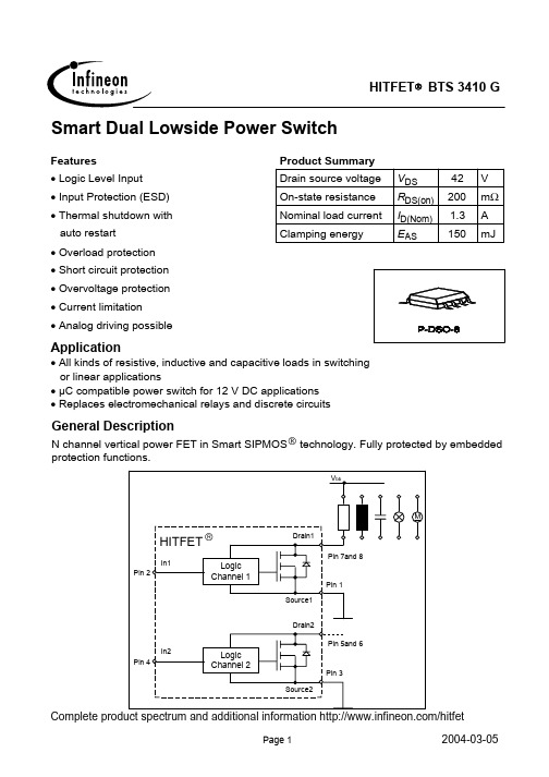
150
50
2
MSL1 40/150/56
Unit V
mA
°C W mJ V
kV
Thermal resistance
junction - ambient: per channel
@ 6 cm2 cooling area2)
one channel on
both channe 160
BTS 3410 G Pin Configuration (Top view)
S1 1· IN1 2 S2 3 IN2 4
P-DSO-8-7
8 D1 7 D1 6 D2 5 D2
â HITFET
Current Limitation
OvervoltageProtection
Drain1
Pin 7, 8
元器件交易网
HITFETÒ BTS 3410 G
Smart Dual Lowside Power Switch
Features · Logic Level Input · Input Protection (ESD) · Thermal shutdown with
auto restart · Overload protection · Short circuit protection · Overvoltage protection · Current limitation · Analog driving possible
Page 3
2004-03-05
元器件交易网
BTS 3410 G
Electrical Characteristics
Parameter
Symbol
at Tj = 25°C, unless otherwise specified Characteristics
北京聚英翱翔电子有限公司USB协议转换器产品说明书

USB协议转换器说明书
北京聚英翱翔电子有限责任公司
2014年08月
产品特点
●宽压供电单独供电
●通讯便捷
●通讯方式支持USB-TTL、RS232、RS485数据传输。
●全隔离,USB供电
●内含RS232、485、TTL芯片
产品功能
●USB-TTL、232、485三合一转换器
●波特率支持2400,4800,9600,19200,38400。
产品选型
型号TTL RS232RS485WiFi继电器USB协议转换器●●●
主要参数
参数说明
耐久性10万次
数据接口RS232RS485TTL USB
额定电压DC7-30V
电源指示1路红色LED指示
通讯指示2路通讯LED指示
尺寸97*50*32mm
重量330g
波特率2400,4800,9600,19200,38400
温度范围工业级,-40℃~85℃
接口定义
管脚定义含义
1USB B型USB接口
2Vcc电源输出+
3Gnd电源输出-
4TX RS232TX
5RX RS232RX
6A+RS485A+
7B-RS485B-
8RXD TTL RX
9TXD TTL TX
接线说明
RS232接线方式:RS485接线方式:TTL接线方式:
测试软件
各种串口调试助手均可使用。
CommScope HT3580H系列四密度全谱宽频分布多路复用(DWDM)发射器系统说明书
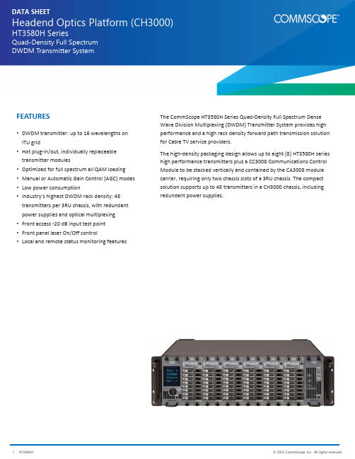
DATA SHEETHeadend Optics Platform (CH3000)HT3580H SeriesQuad-Density Full Spectrum DWDM Transmitter SystemThe CommScope HT3580H Series Quad ‐Density Full Spectrum Dense Wave Division Multiplexing (DWDM) Transmitter System provides high performance and a high rack density forward path transmission solution for Cable TV service providers.The high ‐density packaging design allows up to eight (8) HT3580H series high performance transmitters plus a CC3008 Communications Control Module to be stacked vertically and contained by the CA3008 module carrier, requiring only two chassis slots of a 3RU chassis. The compact solution supports up to 48 transmitters in a CH3000 chassis, including redundant power supplies.•DWDM transmitter: up to 16 wavelengths on ITU grid•Hot plug ‐in/out, individually replaceable transmitter modules•Optimized for full spectrum all QAM loading •Manual or Automatic Gain Control (AGC) modes •Low power consumption•Industry’s highest DWDM rack density: 48 transmitters per 3RU chassis, with redundant power supplies and optical multiplexing •Front access ‐20 dB input test point •Front panel laser On/Off control•Local and remote status monitoring featuresFEATURESWhen installed in the chassis, the transmitters interface to a “zero ‐slot” back plate, providing support for up to eight HT3580H series transmitters. The figure below shows a fully loaded carrier mated to the BD31A8 Quad ‐Density back plate that supports eight HT3580H transmitters.The CC3008 Communications Module installed at the top of a HT3580H series transmitter stack provides the communications interface between the transmitters and the CH3000 mid ‐plane bus, allowing complete configuration and management control of the stack, both local andremote.HT3580H Series Quad ‐Stack and CC3008 Communications Module in CA3008 module carrier joined with a BD31A8 Back PlateHT3580H Series Quad ‐Density Full Spectrum DWDM Transmitters (1.2 GHz Passband)CommScope HT3580H Series Quad ‐Density Full Spectrum DWDM Transmitters are a key element of the CommScope HFC and Fiber Deep architectures in support of the evolution to all QAM transmission. These high ‐performance transmitters are designed for Dense Wave Division Multiplexing (DWDM) applications for point ‐to ‐point forward path transmission of full spectrum broadcast and narrowcast services.HT358xH series transmitters are designed for all QAM loading. These transmitters also incorporate advanced dispersion compensation circuitry to enable transmission of high ‐quality signals over maximum distances.The above figure shows a front view of the CA3008 carrier components: a single HT358xH Quad ‐Density Transmitter (left); a single CC3008 Communications Module (right), and a fully loaded “stack” (center) providing eight (8) DWDM transmitters, requiring only 2 slots of a CH3000 Chassis. A fully loaded CH3000 chassis supports 48 Quad ‐Density DWDM transmitters and redundant power supplies.Features•DWDM transmitter: 16 wavelengths on the ITU grid •Manual or Automatic Gain Control (AGC) modes •RF input attenuation up to ‐6 dB •Optimized for full spectrum loading •HT358xH: All QAM loading•Hot plug ‐in/out, individually insertable•Low power consumption•Industry’s highest DWDM rack density: 48 transmitters per 3RU chassis, with redundant power supplies •Front access ‐20 dB input test point •Front panel laser On/Off interlock control •Local and remote status monitoringHT3580H SERIES SPECIFICATIONSPhysicalDimensions11.5” D x 0.4” H x 2.0” W (29.2 x 1.0 x 5.1 cm)*Weight0.4 lb(0.18 kg)* Eight (8) transmitter units designed to be vertically stacked, plus a CC3008 Communications Module, and installedinside a CA3008 Module Carrier. The combination occupies two slots in a 3RU CH3000 Chassis.EnvironmentalOperating‐20°to +50°C (‐4°to 122°F)Storage‐40°to +85°C (‐40°to +185°F)Humidity5% to 95% non‐condensingRF and Optical InterfacesRF Input F‐type male (located on BD31A8 or BD35M8 Back Plates)RF Test Point75Ω MCX female (located on front panel) MCX male to F female adapter provided with each Quad BD3 back plate.Additional adapters available in packs of ten, order P/N TL3MCXF‐10Optical Connector SC/APC (located on BD35M8 Back Plates)LC/APC (located on BD31A8 Back Plates)Power RequirementsInput Voltage12 VDCPower Consumption6 W (per transmitter) including controller and back plate cooling fanGeneralHot plug‐in/outManual and automatic gain controlChannel LoadingHT358xH: All QAM channelsOpticalOptical Output Power10 ±0.25 dBmWavelength See DWDM ITU Channel Plans descriptionFiber Length60 km max. (Dispersion Compensation adjustable in 1 km steps)•Compatible with external dispersion compensation for some applicationsElectricalPassband45 to 1218 MHzFrequency Response (Including Slope)•±1.0 dB (BC input @ 25°C)•±0.5 dB (NC input relative to BC input)NOTE: NC QAM signals are attenuated 6 dB before internal combining with BCanalog signalsNominal RF Input Levels (Input Attenuator = 0 dB)Broadcast (BC) RF input: 10.2 dBmV 194 256‐QAM channelsNarrowcast (NC) RF input: 16.2 dBmV 194 256‐QAM channelsRF Input Impedance75 Ω, nomRF Input Return Loss18 dB, minRF Input Attenuator/Amplify Range (Manual Mode)‐6.0 to 0 dBRF Input Attenuator Step Size0.5 dBAGC Mode Maintains RF power constant when input RF power changes up to ±3 dB of the learned RF valueLevel Stability (Typical)±0.2 dB256‐QAM BER< 10–6(pre‐FEC, ITU‐C)MER (194 QAM load)40 (40 km), 37 (60 km)DWDM ITU Channel PlansSee muxing back plate information for wavelength graphics. CommScope supports DWDM network architectureswith a variety of products on the standard DWDM ITU Grid (ITU‐T G.694.1). For a more complete description, pleaserefer to the CommScope DWDM ITU Grid Channel Plan data sheet.BD31A8‐100 Quad ‐Density Back PlatesThe BD31A8 models provide RF input and optical connections to or from the HT358xH transmitters. The fan provides air flow to keep transmitters cool.BD31A8‐100‐H10F ‐0‐AL is a quad ‐density back plate that provides 1 common BC input and 8 separate NC RF inputs for eightHT358xH Transmitters. It also supports eight separate optical output LC/APC connectors. Internally it includes an RF amplifier and splitter to split the BC input equally to all 8 transmitters and maintain 1x8 RF levels.BD31A8‐100‐H18F ‐0‐AL is a quad ‐density back plate that provides 8 separate BC inputs and 0 NC RF input for eight HT358xH Transmitters. It also supports eight separate optical output LC/APC connectors. This back plate is recommended for customers that prefer to do their broadcast and narrowcast RF combining external from the CH3000 Chassis.BD31A8‐100‐H10F ‐0‐AL Back Plate CA3008 Module CarrierBD31A8 BACK PLATE SPECIFICATIONSSpecificationPhysical Dimensions 7.2” D x 5.2” H x 2.0” W (18.2 x 13.0x 5.4cm)Weight 2.0 lb (0.91 kg)Environmental Operating ‐20°to +65°C (‐4°to 149°F)Storage ‐40°to +85°C (‐40°to +185°F)Humidity5% to 95% non ‐condensingPower Requirements Input Voltage 12 V DCPower Consumption 5.5 W max (2.5 W Typ),included in power figure found in HT3580H specifications OpticalThrough 8 LC/APC connectors, the BD31A8‐100 provides optical pass ‐through from the HT358xH transmitter.Optical Insertion Loss 0.2 dB Typ; 0.3 dB Max RF InterfaceThe BD31A8 provides RF to the HT358xH transmitter through F ‐type RF connectors.•1 BC and 8 NC (BD31A8‐100‐H10F ‐0‐AL)•8 BC and 0 NC (BD31A8‐100‐H18F ‐0‐AL)BD35M8‐ACx and BD35M8‐EEx Quad‐Density Back Plates for Groups of 8 WavelengthsThe CommScope BD35M8 Family of back plates are 100 GHz grid spacing Quad‐Density Mux Back Plates that multiplex the output of eight HT3580H Quad‐Density Full Spectrum Transmitters.These back plates provide connections for a group of eight HT3580H Series Transmitters installed in the same CA3008 Module Carrier, along with the CC3008 Communications Control Module.These 8‐channel mux back plates (for which outputs can be cascaded from one back plate to another) may be ordered for the channel groups indicated in the ordering information section.BD35M8 BACK PLATE SPECIFICATIONSPhysicalDimensions7.2” D x 5.2” H x 2.0” W (18.2 x 13.0x 5.4cm)Weight 2.0 lb(0.91 kg)EnvironmentalOperating‐20°to +65°C (‐4°to 149°F)Storage‐40°to +85°C (‐40°to +185°F)Humidity5% to 95% non‐condensingPower RequirementsInput Voltage12 V DCPower Consumption5 W max (2.5 W Typ), included in power figure found in HT3580H specificationsOptical InterfaceOptical Connectors SC/APC (3)•DWDM INP (input from previous mux back plate)•DWDM OUT (output to network or next mux back plate)•‐20 dB optical test pointRF Interface9 F‐Type Connectors•1 BC and 8 NCOpticalChannel Spacing100 GHzChannel Plan See ITU Channels in Ordering InformationInsertion Losses, Including ConnectorsTyp Max•DWDM Input to DWDM Output 1.8 dB 2.1 dB•Ch. yy Input to DWDM Output 2.0 dB 2.4 dB•‐20 dB Test Point 20.0 dB 20.4 dBUniformity, Including Connectors•Module Uniformity 1.1 dB 1.5 dB•Paired Uniformity0.5 dB0.7 dBReturn Loss, min45 dBDirectivity, min55 dBPassband @ 0.2 dB•Ch. yy Input to DWDM Output±0.125 nm•DWDM Input to DWDM Output Passes 1423.5 through 1617.5 with a notch at the channel add/drop band. WDL for the passband is within ±0.15 dB Polarization Dependent Loss, max0.15 dB (typically < 0.05 dB)Power Handling, max (Any Input Port)21.8 dBmBD35M8‐DCx Quad‐Density Back Plates for 2 Sets for the Same Group of 4 WavelengthsThe CommScope BD35M8 Family of back plates are 100 GHz grid spacing Quad‐Density Mux Back Plates that multiplex the output of 2 sets of four HT3580H Quad‐Density Full Spectrum Transmitters onto two separate output ports.These back plates allow 2 sets of four HT3580H Series Transmitters installed in the same CA3008 Module Carrier, and using the same CC3008 Communications Control Module, to feed two different fibers with four wavelengths on each fiber.These 2x4‐channel mux back plates (for which outputs can be cascaded from one back plate to another) that may be ordered for the channel groups indicated in the ordering information section.BD35M8 BACK PLATE SPECIFICATIONSPhysicalDimensions7.2” D x 5.2” H x 2.0” W (18.2 x 13.0x 5.4cm)Weight 2.0 lb(0.91 kg)EnvironmentalOperating‐20°to +65°C (‐4°to 149°F)Storage‐40°to +85°C (‐40°to +185°F)Humidity5% to 95% non‐condensingPower RequirementsInput Voltage12 V DCPower Consumption5 W max (2.5 W Typ), included in power figure found in HT3580H specificationsOptical InterfaceOptical Connectors LC/APC (6)•2 of DWDM INP (input from previous mux back plate)•2 of DWDM OUT (output to network or next mux back plate)•2 of ‐20 dB optical test pointRF Interface9 F‐Type Connectors•1 BC and 8 NCOpticalChannel Spacing100 GHzChannel Plan See ITU Channels in Ordering InformationInsertion Losses, Including ConnectorsTyp Max•DWDM Input to DWDM Output 1.1 dB 1.3 dB•Ch. yy Input to DWDM Output 1.3 dB 1.5 dB•‐20 dB Test Point 20.0 dB 20.4 dBUniformity, Including Connectors•Module Uniformity0.4 dB0.5 dB•Paired Uniformity0.5 dB0.7 dBReturn Loss, min45 dBDirectivity, min55 dBPassband @ 0.2 dB•Ch. yy Input to DWDM Output±0.125 nm•DWDM Input to DWDM Output Passes 1423.5 through 1617.5 with a notch at the channel add/drop band. WDL for the passband is within ±0.15 dB Polarization Dependent Loss, max0.1 dB (typically < 0.05 dB)Power Handling, max (Any Input Port)21.8 dBmH T 358*H –Q –***0–2–A SQuad ‐Density, Full Spectrum DWDM Transmitter (1.2 GHz)3 = EEx Wavelengths (See BD35M8 Table Below)4 = ACx Wavelengths (See BD35M8 Table Below)For HT3583H = E + ** ITU Channel #For HT3584H = A + ** ITU Channel #** = ITU Channel Number (20 through 62;See CommScope DWDM ITU Grid Channel Plan Data Sheet)Connector Type: SC/APCHT358xH TransmitterConnector Type: SC/APCBack PlatesB D 31A 8–100–H 1x F –0–A LB D 35M 8–***–H 20F –3–A SHT3584H16 Wavelength Plan Code Wavelength Group AC2ITU CH 20, 21, 24, 29ITU CH 35, 42, 52, 54AC4ITU CH 23, 33, 44, 47ITU CH 51, 57, 58, 59HT3583H16 Wavelength Plan Code Wavelength Group EEBITU CH 21, 22, 24, 26ITU CH 28, 33, 36, 39EED ITU CH 44, 48, 52, 54ITU CH 57,60, 61,62Quad ‐Density Back Plate for 8 HT358x Full Spectrum Transmitters with LC/APC Connector 0 = 1 Common BC Input and 8 NC RF Inputs 8 = 8 BC Inputs and 0 NC RF Input Connector Type: LC/APCQuad ‐Density Muxing Back Plate for 8 HT358x Full Spectrum Transmitters with SC/APC Connectors with Optical Test Point0 = 1 Common BC Input and 8 NC RF InputsConnector Type: LC/APCB D 35M 8–D **–H 20F –3–A LHT3584H 2 sets of 4 of the 16 Wavelength Plan Code Wavelength Group DC1ITU CH 20, 21, 24, 29ITU CH 20, 21, 24, 29Quad ‐Density Muxing Back Plate for 2 Sets of 4 of the HT358x Full Spectrum Transmitters with LC/APC Connectors with Optical Test Point 0 = 1 Common BC Input and 8 NC RF InputsSystem AccessoriesContact Customer Care for product information and sales:•United States: 866‐36‐ARRIS •International: +1‐678‐473‐5656RELATED PRODUCTSCH3000 Chassis Optical Patch Cords Optical Transmitters Optical Passives Digital ReturnInstallation ServicesNote: Specifications are subject to change without notice.Copyright Statement:©2022CommScope,Inc.All rights reserved.ARRIS and the ARRIS logo are trademarks of CommScope,Inc.and/or its affiliates.All other trademarks are the property of their respective owners.No part of this content may be reproduced in any form or by any means or used to make any derivative work (such as translation,transformation,or adaptation)without writtenpermission from CommScope,Inc and/orits affiliates (“CommScope”).CommScope reserves the right to revise or change this content from time to time without obligation on the part of CommScope to provide notification of such revision or change.C C 3008Communications Control ModuleC A 3008Module CarrierH T 3F I L HFiller Module for Quad ‐Density Slots。
Latitude 3580 用户手册说明书

Latitude 3580用户手册6 2021注意、小心和警告:“注意”表示帮助您更好地使用该产品的重要信息。
:“小心”表示可能会损坏硬件或导致数据丢失,并告诉您如何避免此类问题。
:“警告”表示可能会导致财产损失、人身伤害甚至死亡。
版权所有 © 2017 Dell Inc. 或其附属公司。
保留所有权利。
Dell、EMC 和其他商标均为 Dell Inc. 或其附属公司的商标。
其他商标均为其各自所有者的商标。
章 1: 拆装计算机内部组件 (6)安全说明 (6)关闭计算机— Windows 10 (6)关闭计算机 (7)关闭计算机— Windows 7 (7)拆装计算机内部组件之前 (7)拆装计算机内部组件之后 (8)章 2: 卸下和安装组件 (9)建议工具 (9)螺钉大小列表 (9)基座盖 (10)卸下基座护盖 (10)安装基座护盖 (12)电池 (12)锂离子电池预防措施 (12)卸下电池 (12)安装电池 (13)键盘 (13)卸下键盘 (13)安装键盘 (17)WLAN 卡 (17)卸下 WLAN 卡 (17)安装 WLAN 卡 (18)WWAN 卡 (18)卸下 WWAN 卡 (18)安装 WWAN 卡 (19)内存模块 (19)卸下内存模块 (19)安装内存模块 (20)硬盘驱动器 (HDD) (20)卸下硬盘驱动器 (HDD) (20)安装硬盘驱动器 (HDD) (22)章 3: 技术规格 (23)系统规格 (23)处理器规格 (23)内存规格 (23)硬盘驱动器选项 (24)音频规格 (24)视频规格 (24)摄像头规格 (25)通信规格 (25)端口和连接器规格 (25)目录3触摸板规格 (26)电池规格 (27)交流适配器规格 (27)物理规格 (28)环境规格 (28)章 4: 技术和组件 (29)电源适配器 (29)处理器 (29)在任务管理器中验证处理器使用率 (29)在资源监视器中验证处理器使用率 (29)在 Windows 10 中识别处理器 (30)在 Windows 8.1 中识别处理器 (30)在 Windows 7 中识别处理器 (30)芯片组 (30)在 Windows 10 的设备管理器中识别芯片组 (30)在 Windows 8.1 的设备管理器中识别芯片组 (30)在 Windows 7 的设备管理器中识别芯片组 (30)Intel HD Graphics (31)显示屏选项 (31)识别显示屏适配器(Windows 7 和 Windows 10) (31)更改屏幕分辨率(Windows 7、8.1 和 10) (31)在 Windows 10 中调节亮度 (31)在 Windows 8.1 中调节亮度 (31)在 Windows 7 中调节亮度 (32)连接到外部显示屏设备(Windows 7、8.1 和 10) (32)DDR4 (32)内存特性 (33)验证系统内存 (33)验证系统安装程序 (BIOS) 中的系统内存 (33)使用 ePSA 测试内存 (34)硬盘驱动器选项 (34)在 Windows 10 中识别硬盘驱动器 (34)在 Windows 8.1 中识别硬盘驱动器 (34)在 Windows 7 中识别硬盘驱动器 (34)在 BIOS 中识别硬盘驱动器 (34)USB 功能 (35)HDMI 1.4 (37)Realtek ALC3246 (37)摄像头功能 (37)启动摄像头(Windows 7、8.1 和 10) (37)启动摄像头应用程序 (37)章 5: 系统设置选项 (39)引导顺序 (39)导航键 (39)系统设置程序概览 (39)4目录系统配置屏幕选项 (40)视频屏幕选项 (41)安全性屏幕选项 (41)安全引导屏幕选项 (43)性能屏幕选项 (43)电源管理屏幕选项 (44)POST 行为屏幕选项 (45)无线屏幕选项 (45)维护屏幕选项 (45)系统日志屏幕选项 (46)SupportAssist 系统分辨率 (46)在 Windows 中更新 BIOS (46)使用 USB 闪存驱动器更新系统 BIOS (47)系统密码和设置密码 (48)分配系统密码和设置密码 (48)删除或更改现有系统密码和/或设置密码 (48)章 6: 故障排除 (50)增强型预引导系统评估 (ePSA) 诊断程序 (50)运行 ePSA 诊断程序 (50)章 7: 联系戴尔 (51)目录5拆装计算机内部组件安全说明遵循以下安全原则可防止您的计算机受到潜在损坏并确保您的人身安全。
- 1、下载文档前请自行甄别文档内容的完整性,平台不提供额外的编辑、内容补充、找答案等附加服务。
- 2、"仅部分预览"的文档,不可在线预览部分如存在完整性等问题,可反馈申请退款(可完整预览的文档不适用该条件!)。
- 3、如文档侵犯您的权益,请联系客服反馈,我们会尽快为您处理(人工客服工作时间:9:00-18:30)。
Optoway BTR-3580G*********************************************************************************************************************************************************************************************************************************************************************************************************************************************OPTOWAY TECHNOLOGY INC. No .38, Kuang Fu S. Road, Hu Kou, Hsin Chu Industrial Park, Hsin Chu, Taiwan 303Tel: 886-3-5979798 Fax: 886-3-59797371BTR-3580G / BTR-3580-SPG1550 nm TX / 1310 nm RX , 5V / 155 Mbps RoHS Compliant Single-Fiber Transceiver**********************************************************************************************************************************************************************FEATURESl Single Fiber Bi-Directional Transceiver l 1550 nm DFB LD Transmitter l 1310 nm Receiver l Distance Up to 80 kml Industry Standard 1 x 9 Footprint l Single +5 V Power Supply l RoHS Compliantl PECL Differential Inputs and Outputs l 0 to 70o C Operating Temperaturel Wave Solderable and Aqueous Washablel Class 1 Laser International Safety Standard IEC-60825 CompliantAPPLICATIONSl WDM 155 Mb/s Linksl SONET/SDH Equipment Interconnect l Fast Ethernet 100 Mb/s LinksDESCRIPTIONThe BTR-3580G series is high performance module for single fiber communications by using 1550 nm transmitter and 1310 nm receiver. The transmitter section uses a multiple quantum well DFB laser and is a class 1 laser compliant according to International Safety Standard IEC-60825. The receiver section uses an integrated 1310 nm detector preamplifier (IDP) mounted in an optical header and a limiting post-amplifier IC. A PECL logic interface simplifies interface to external circuitry.LASER SAFETYThis single mode transceiver is a Class 1 laser product. It complies with IEC-60825 and FDA 21 CFR 1040.10 and 1040.11. The transceiver must be operated within the specified temperature and voltage limits. The optical ports of the module shall be terminated with an optical connector or with a dust plug.ORDER INFORMATIONP/No.Bit Rate (Mb/s) Distance(km) TX(nm) RX (nm) Voltage (V) Package Temp (o C) TX Power (dBm) RX Sens. (dBm) RoHS Compliant BTR-3580G125/155801550 DFB131051X90 to 702 to -3 -35 YesNote: 1. BTR-XXXXXG is 1X9 SC receptacle type package.2. BTR-XXXXX-XPBBBG is 1X9 pigtail type package with different connector, A=S is SC connector, A=F is FCconnector, A=T is ST connector, A=L is LC connector, A=M is MU connector; BBB is the length of fiber in cm.Absolute Maximum RatingsParameterSymbol Min Max Units NotesStorage Temperature Tstg -40 85 o COperating Temperature Topr 0 70 o CSoldering Temperature --- 260 o C 10 seconds on leads only Power Supply Voltage Vcc 0 6 V Input Voltage --- GND Vcc V Output CurrentIout30mARecommended Operating ConditionsParameterSymbol Min Typ Max Units Power Supply Voltage Vcc 4.75 5.00 5.25 V Operating Temperature Topr 0 70 o C Data Rate155 170 Mb/s Power Supply CurrentIcc280mA***********************************************************************************************************************************************************************OPTOWAY TECHNOLOGY INC. No .38, Kuang Fu S. Road, Hu Kou, Hsin Chu Industrial Park, Hsin Chu, Taiwan 303Tel: 886-3-5979798 Fax: 886-3-5979737Transmitter Specifications (0o C < Topr < 70o C, 4.75V < Vcc < 5.25V)ParameterSymbolMinTypMaxUnitsNotesOpticalOptical Transmit Power Po -3 --- 2 dBm 1Output Center Wavelength λ1480 1580 nm Output Spectrum Width ∆λ--- --- 1 nm -20 dB Width Extinction Ratio E R 10 --- --- dB Output EyeCompliant with Bellcore GR-253-CORE and ITU recommendation G.957Optical Rise Time t r 2 ns 10% to 90% Values Optical Fall Timet f 2 ns 10% to 90% Values Relative Intensity Noise RIN -116 dB/Hz Total Jitter TJ 1.0 ns 2 ElectricalData Input Current – Low I IL -350 µA Data Input Current – High I IH 350 µA Differential Input Voltage V IH - V IL 300 mVData Input Voltage – Low V IL - V CC -2.0 -1.58 V 3 Data Input Voltage -- HighV IH - V CC-1.1-0.74V3Notes: 1. Output power is power coupled into a 9/125 µm single mode fiber.2. Measured with a 223-1 PRBS with 72 ones and 72 zeros.3. These inputs are compatible with 10K, 10KH and 100K ECL and PECL inputs.Receiver Specifications (0o C < Topr < 70o C, 4.75 V < Vcc < 5.25V)ParameterSymbol Min Typ Max Units Notes Optical Sensitivity--- --- --- -35 dBm 1Maximum Input Power Pin -3 --- --- dBmSignal Detect -- Asserted Pa --- --- -35 dBm Transition: low to high Signal Detect -- Deasserted Pd -43 --- --- dBm Transition: high to low Signal detect -- Hysteresis 1.0 --- 4.0 dBWavelength of Operation 1260 1360 nm 2ElectricalData Output Voltage – Low V OL - V CC -2.0 -1.58 V 3 Data Output Voltage – High V OH - V CC -1.1 -0.74 V 3 Signal Detect Output Voltage -- LowV OL - V CC -2.0 -1.58 V 3 Signal Detect Output Voltage -- HighV OH - V CC-1.1-0.74V3Notes: 1.Minimum sensitivity and saturation levels at BER 1E-=10 for a 223-1 PRBS with 72 ones and 72 zeros. 2. At least 30 dB optical isolation for the wavelength 1480 to 1580 nm.3. These outputs are compatible with 10K, 10KH and 100K ECL and PECL outputs.CONNECTION DIAGRAMReceiver Signal Ground 1 (Rx GND)Receiver Data Out 2 (RD+) N/CReceiver Data Out Bar 3 (RD−)Signal Detect 4 (SD)Receiver Power Supply 5 (Rx Vcc) TOP VIEWTransmitter Power Supply 6 (Tx Vcc)Transmitter Data In Bar 7 (TD−)Transmitter Data In 8 (TD+) N/C Transmitter Signal Ground 9 (Tx GND)PACKAGE DIAGRAMUnits in mm*********************************************************************************************************************************************************************** OPTOWAY TECHNOLOGY INC. No.38, Kuang Fu S. Road, Hu Kou, Hsin Chu Industrial Park, Hsin Chu, Taiwan 303Tel: 886-3-5979798 Fax: 886-3-5979737。