Lllx1-h
LD—RH—CC工艺生产H08A的实践

热送( 冷送 ) 高速 线 材厂 。 针对 这 些 技 术 难 点进 行 新 的工 艺 流 程设 计 , 改
进后 的工 艺 流程 为铁 水 ( 硫 扒 渣 ) l0t 吹转 脱 一 o 复 炉一 氩站 一 l o tR 炉 3号 方 坯 连 铸 机 一 热 送 0 H
( 送 ) 速线 材 厂 。 冷 高
参照 该产 品 的 国家标准 制定 了 H 8 0 A钢 的 内控 成分 , 见表 1 。
收 稿 日期 :0 90 -7 2 0 -82
作者简介 : 杜家恩( 9 3) 男 , 1 8 一 , 福建福鼎人 , 助理工程 师 , 事炼钢工艺管理工作。 从
・
1 ・ 0
江
西
冶
金
21 0 0年 6月
Ke o d s li g p o e s de o i ai n; o tn o a tn y W r s: metn r c s ; s x d t o c n i u usc si g
0 前 言
低碳 低 硅 焊 接 用 钢 H 8 主要 用 于制 造 焊 条 、 0A 焊 芯及 焊丝 。近 年来 , 随着焊 接构 件 的广 泛应用 , 焊
杜 家恩 , 建刚 , 陈 陈登 国
( 余钢铁有限责任公 司 , 新 江西 新余 380 ) 3 0 1
摘
要 : 通过优化 H 8 0A钢冶炼工艺路线, 转炉采用双渣法操作, 放钢过程不加合金 , 吹氩、 H炉脱 R
氧、 脱气 、 升温 等处理 , 节约 了脱 氧剂用量 , 降低 了生 产成本 , 钢水流 动性好 , 铸坯没有皮 下气泡 缺陷。
关
键
词 : 冶炼 工艺 ; 氧 ; 脱 连铸 F 2
2009微机原理习题
2009微机原理习题一、填空题:1.计算机是通过____________、____________、____________总线把各个部件连接在一起,构成一个系统。
(数据、地址、控制)2.微处理器的字长是指____________________。
(一次处理二进制位数)3.微处理器的主频是指____________________。
(处理器时钟频率)4.8086CPU有________根数据线,________根地址线,可寻址的地址空间达到________字节,数据总线与地址总线是以________________方式复用,其经加电复位后,执行第一条指令的物理地址是________________。
(16、20、1M、分时、FFFF0H)5.从功能上,8086CPU可分为________________和________________两部分。
(总线接口单元BIU、执行单元 EU)6.8086/8088CPU内部共有________个________位寄存器。
(14、16)7.8086/8088CPU内部共有________个________位段寄存器,分别是________、________、________和________,用来存放16位的________。
(4、16、CS、DS、SS、ES、段基地址)8.8086/8088CPU内部用来存放下一条要执行的指令的偏移地址的寄存器是________,它与段寄存器________配合产生下一条要执行的指令的________地址。
(IP、CS、物理)9.8086/8088CPU内部标志寄存器________用来存放6个________标志位和3个________标志位。
(FLAGS、状态、控制)10.8086/8088CPU内部共有________个16位通用寄存器,其中________、________、________和________可分别分为2个8位寄存器使用。
saa7111a

DATA SHEETProduct specification Supersedes data of 1997May26 File under Integrated Circuits, IC221998May15SAA7111AEnhanced Video Input Processor (EVIP)Enhanced Video Input Processor (EVIP)SAA7111ACONTENTS1FEATURES2APPLICATIONS3GENERAL DESCRIPTION4QUICK REFERENCE DATA5ORDERING INFORMATION6BLOCK DIAGRAM7PINNING8FUNCTIONAL DESCRIPTION8.1Analog input processing8.2Analog control circuits8.2.1Clamping8.2.2Gain control8.3Chrominance processing8.4Luminance processing8.5RGB matrix8.6VBI-data bypass8.7VPO-bus (digital outputs)8.8Reference signals HREF, VREF and CREF 8.9Synchronization8.10Clock generation circuit8.11Power-on reset and CE input8.12RTCO output8.13The Line-21 text slicer8.13.1Suggestions for I2C-bus interface of the displaysoftware reading line-21 data9BOUNDARY-SCAN TEST9.1Initialization of boundary-scan circuit9.2Device identification codes10GAIN CHARTS11LIMITING VALUES12CHARACTERISTICS13TIMING DIAGRAMS14CLOCK SYSTEM14.1Clock generation circuit14.2Power-on control15OUTPUT FORMATS16APPLICATION INFORMATION16.1Layout hints17I2C-BUS DESCRIPTION17.1I2C-bus format17.2I2C-bus detail 17.2.1Subaddress0017.2.2Subaddress0217.2.3Subaddress0317.2.4Subaddress0417.2.5Subaddress0517.2.6Subaddress0617.2.7Subaddress0717.2.8Subaddress0817.2.9Subaddress0917.2.10Subaddress0A17.2.11Subaddress0B17.2.12Subaddress0C17.2.13Subaddress0D17.2.14Subaddress0E17.2.15Subaddress1017.2.16Subaddress1117.2.17Subaddress1217.2.18Subaddress1317.2.19Subaddress1517.2.20Subaddress1617.2.21Subaddress1717.2.22Subaddress 1A (read-only register)17.2.23Subaddress 1B (read-only register)17.2.24Subaddress 1C (read-only register)17.2.25Subaddress 1F (read-only register)18FILTER CURVES18.1Anti-alias filter curve18.2TUF-block filter curve18.3Luminance filter curves18.4Chrominance filter curves19I2C-BUS START SET-UP20PACKAGE OUTLINES21SOLDERING21.1Introduction21.2Reflow soldering21.3Wave soldering21.4Repairing soldered joints22DEFINITIONS23LIFE SUPPORT APPLICATIONS24PURCHASE OF PHILIPS I2C COMPONENTSEnhanced Video Input Processor (EVIP)SAA7111A1FEATURES•Four analog inputs, internal analog source selectors,e.g. 4×CVBS or 2×Y/C or (1×Y/C and2×CVBS)•Two analog preprocessing channels•Fully programmable static gain for the main channels orautomatic gain control for the selected CVBS or Y/C channel•Switchable white peak control•Two built-in analog anti-aliasing filters•Two 8-bit video CMOS analog-to-digital converters •On-chip clock generator•Line-locked system clock frequencies•Digital PLL for horizontal-sync processing and clock generation•Requires only one crystal (24.576MHz) for all standards •Horizontal and vertical sync detection•Automatic detection of 50and60Hz field frequency, and automatic switching between PAL and NTSC standards•Luminance and chrominance signal processing for PAL BGHI, PAL N, PAL M, NTSC M, NTSC N,NTSC4.43, NTSC-Japan and SECAM•User programmable luminance peaking or aperture correction•Cross-colour reduction for NTSC by chrominance comb filtering•PAL delay line for correcting PAL phase errors•Real time status information output (RTCO)•Brightness Contrast Saturation (BCS) control on-chip •The YUV (CCIR-601) bus supports a data rate of:–864×f H=13.5MHz for 625line sources–858×f H=13.5MHz for 525line sources.•Data output streams for16,12or8-bit width with the following formats:–YUV4:1:1 (12-bit)–YUV4:2:2 (16-bit)–YUV4:2:2 (CCIR-656) (8-bit)–RGB(5,6,and5) (16-bit) with dither–RGB(8,8,and8) (24-bit) with special application.•Odd/even field identification by a non interlace CVBS input signal•Fix level for RGB output format during horizontal blanking•720active samples per line on the YUV bus•One user programmable general purpose switch on an output pin•Built-in line-21 text slicer•A 27MHz Vertical Blanking Interval (VBI) data bypass programmable by I2C-bus for INTERCAST applications •Power-on control•Two via I2C-bus switchable outputs for the digitized CVBS or Y/C input signals AD1(7to0) and AD2(7to0)•Chip enable function (reset for the clock generator and power save mode up from chip version3)•Compatible with memory-based features (line-locked clock)•Boundary scan test circuit complies with the‘IEEE Std. 1149.1−1990’ (ID-Code=0F11102B)•I2C-bus controlled (full read-back ability by an external controller)•Low power (<0.5W), low voltage (3.3V), small package (LQFP64)•5V tolerant digital I/O ports.2APPLICATIONS•Desktop/Notebook (PCMCIA) video•Multimedia•Digital television•Image processing•Video phone•Intercast.Enhanced Video Input Processor (EVIP)SAA7111A3GENERAL DESCRIPTIONThe Enhanced Video Input Processor (EVIP) is a combination of a two-channel analog preprocessing circuit including source selection, anti-aliasing filter and ADC, an automatic clamp and gain control, a Clock Generation Circuit (CGC), a digital multi-standard decoder (PAL BGHI, PAL M, PAL N, NTSC M,NTSC-Japan NTSC N and SECAM), abrightness/contrast/saturation control circuit, a colour space matrix (see Fig.1) and a 27MHz VBI-data bypass.The pure 3.3V CMOS circuit SAA7111A, analogfront-end and digital video decoder, is a highly integrated circuit for desktop video applications. The decoder is based on the principle of line-locked clock decoding and is able to decode the colour of PAL, SECAM and NTSC signals into CCIR-601 compatible colour component values. The SAA7111A accepts as analog inputs CVBS or S-video (Y/C) from TV or VTR sources. The circuit is I 2C-bus controlled. The SAA7111A then supports several text features as Line 21 data slicing and a high-speed VBI data bypass for Intercast.4QUICK REFERENCE DATA 5ORDERING INFORMATION SYMBOLPARAMETERMIN.TYP .MAX.UNITV DDD digital supply voltage 3.0 3.3 3.6V V DDA analog supply voltage3.1 3.3 3.5V T amb operating ambient temperature 02570°C P A+D analog and digital power−0.5−WTYPE NUMBERPACKAGENAME DESCRIPTIONVERSION SAA7111AHZ LQFP64plastic low profile quad flat package; 64leads; body 10×10×1.4mm SOT314-2SAA7111AHQFP64plastic quad flat package; 64leads (lead length 1.6mm);body 14×14×2.7mmSOT393-1Enhanced Video Input Processor (EVIP)SAA7111A6BLOCK DIAGRAMFig.1 Block diagram.handbook, full pagewidthSDA XTAL XTALI RESIICSA TRST TDI HS VSCLOCK GENERATION CIRCUIT POWER-ON CONTROLINTERFACEI 2C-BUS SYNCHRONIZATIONCIRCUITLUMINANCE CIRCUITSAA7111ACHROMINANCECIRCUIT ANDBRIGHTNESSCONTRASTSATURATION CONTROLVBI DATA BYPASS UPSAMPLING FILTERI 2C-BUS CONTROL CLOCKS Y31ANALOG PROCESSINGANDANALOG-TO-DIGITAL CONVERSION AI11AI12AI21AI22121086AD2AD1ANALOG CONTROLCONBYPASS302717292860151624RTS0555*******LLC2CREF 5234 to 3942 to 5153FEI HREFVPO (0 : 15)GPSW 63626123V SSSn.c.n.c.641013AOUT 14RTCOCEMGG061RTS1LLC V SSA0V DDA0VSSD1-5V DDD1-557,41,33,25,1856,40,32,26,19V SSA1-2VDDA1-29,511,7Y/CVBSC/CVBS TCK 5945823TMS TDOVREF YUV-to-RGB CONVERSIONAND OUTPUT FORMATTERUV YPROCESSING YLFCOTEST CONTROL BLOCK FOR BOUNDARY SCAN TESTAND SCAN TESTSCLEnhanced Video Input Processor (EVIP)SAA7111A 7PINNINGSYMBOLPINI/O/P DESCRIPTION (L)QFP64n.c.1−Do not connect.TDO2O Test data output for boundary scan test; note1.TDI3I Test data input for boundary scan test; note1.TMS4I Test mode select input for boundary scan test or scan test; note1.V SSA25P Ground for analog supply voltage channel2.AI226I Analog input22.V DDA27P Positive supply voltage for analog channel2 (+3.3V).AI218I Analog input21.V SSA19P Ground for analog supply voltage channel1.AI1210I Analog input12.V DDA111P Positive supply voltage for analog channel1 (+3.3V).AI1112I Analog input11.V SSS13P Substrate ground connection.AOUT14O Analog test output; for testing the analog input channels.V DDA015P Positive supply voltage for internal Clock Generator Circuit (CGC) (+3.3V).V SSA016P Ground for internal CGC.VREF17O Vertical reference output signal (I2C-bit COMPO=0) or inverse composite blankingsignal (I2C-bit COMPO=1) (enabled via I2C-bus bit OEHV).V DDD518P Digital supply voltage5 (+3.3V).V SSD519P Ground for digital supply voltage5.LLC20O Line-locked system clock output (27MHz).LLC221O Line-locked clock1⁄2output (13.5MHz).CREF22O Clock reference output: this is a clock qualifier signal distributed by the internal CGCfor a data rate of LLC2. Using CREF all interfaces on the VPO bus are able togenerate a bus timing with identical phase. If CCIR656format is selected(OFTS0=1 and OFTS1=1) an inverse composite blanking signal (pixel qualifier) isprovided on this pin.RES23O Reset output (active LOW); sets the device into a defined state. All data outputs arein high impedance state. The I2C-bus is reset (waiting for start condition).CE24I Chip enable; connection to ground forces a reset, up from version3 power savefunction additionally available.V DDD425P Digital supply voltage input4 (+3.3V).V SSD426P Ground for digital supply voltage input4.HS27O Horizontal sync output signal (programmable); the positions of the positive andnegative slopes are programmable in 8LLC increments over a complete line(equals64µs) via I2C-bus bytes HSB and HSS. Fine position adjustment in 2LLCincrements can be performed via I2C-bus bits HDEL1 and HDEL0.RTS128O Two functions output; controlled by I2C-bus bit RTSE1.RTSE1=0: PAL line identifier (LOW=PAL line); indicates the inverted andnon-inverted R−Y component for PAL signals. RTSE1=1: H-PLL locked indicator;a high state indicates that the internal horizontal PLL has locked.Enhanced Video Input Processor (EVIP)SAA7111ARTS029OTwo functions output; controlled by I 2C-bus bit RTSE0.RTSE0=0: odd/even field identification (HIGH =odd field). RTSE0=1: verticallocked indicator; a HIGH state indicates that the internal Vertical Noise Limiter (VNL)has locked.VS 30OVertical sync signal (enabled via I 2C-bus bit OEHV); this signal indicates the vertical sync with respect to the YUV output. The HIGH period of this signal is approximately six lines if the VNL function is active. The positive slope contains the phase information for a deflection controller.HREF 31OHorizontal reference output signal (enabled via I 2C-bus bit OEHV); this signal is used to indicate data on the digital YUV bus. The positive slope marks the beginning of a new active line. The HIGH period of HREF is 720Y samples long. HREF can be used to synchronize data multiplexer/demultiplexer. HREF is also present during the vertical blanking interval.V SSD332P Ground for digital supply voltage input 3.V DDD333P Digital supply voltage 3 (+3.3V).VPO(15to 10)34to 39ODigital VPO-bus (Video Port Out) signal; higher bits of the 16-bit VPO-bus or the 16-bit RGB-bus output signal. The output data rate, the format and multiplexingscheme of the VPO-bus are controlled via I 2C-bus bits OFTS0 and OFTS1. If I 2C-bus bit VIPB =1 the six MSBs of the digitized input signal are connected to these outputs,configured by the I 2C-bus ‘MODE’ bits (see Figs 33to 40):LUMA →VPO15to VPO8, CHROMA →VPO7to VPO0.V SSD240P Ground for digital supply voltage input 2.V DDD241P Digital supply voltage 2 (+3.3V).VPO (9to 0)42to 51ODigital VPO-bus output signal; lower bits of the 16-bit YUV-bus or the 16-bit RGB-bus output signal. The output data rate, the format and multiplexing schema of theVPO-bus are controlled via I 2C-bus bits OFTS0 and OFTS1. If I 2C-bus bit VIPB =1the digitized input signal are connected to these outputs, configured by the I 2C-bus ‘MODE’ bits (see Figs 33to 40): LUMA →VPO15to VPO8,CHROMA →VPO7to VPO0.FEI 52IFast enable input signal (active LOW); this signal is used to control fast switching on the digital YUV-bus. A HIGH at this input forces the IC to set its Y and UV outputs to the high impedance state.GPSW 53O General purpose switch output; the state of this signal is set via I 2C-bus control and the levels are TTL compatible.XTAL 54O Second terminal of crystal oscillator; not connected if external clock signal is used.XTALI 55I Input terminal for 24.576MHz crystal oscillator or connection of external oscillator with CMOS compatible square wave clock signal.V SSD156P Ground for digital supply voltage input 1.V DDD157P Digital supply voltage input 1 (+3.3V).TRST 58I Test reset input not (active LOW), for boundary scan test; notes 1,2and 3.TCK 59I Test clock for boundary scan test; note 1.RTCO60OReal time control output: contains information about actual system clock frequency,subcarrier frequency and phase and PAL sequence.SYMBOL PIN I/O/P DESCRIPTION(L)QFP64Enhanced Video Input Processor (EVIP)SAA7111ANotes1.In accordance with the ‘IEEE1149.1’ standard the pads TCK, TDI, TMS and TRST are input pads with an internalpull-up transistor and TDO a 3-state output pad.2.This pin provides easy initialization of BST circuit.TRST can be used to force the TAP (Test Access Port) controllerto the Test-Logic-Reset state (normal operation) at once.3.For board design without boundary scan implementation (pin compatibility with the SAA7110) connect the TRST pinto ground.IICSA61II 2C-bus slave address select;0=48H for write, 49H for read 1=4AH for write, 4BH for read.SDA 62I/O Serial data input/output (I 2C-bus).SCL 63I/O Serial clock input/output (I 2C-bus).n.c.64−Not connect.SYMBOL PIN I/O/P DESCRIPTION(L)QFP64Enhanced Video Input Processor (EVIP)SAA7111AFig.2 Pin configuration (LQFP64/QFP64).handbook, full pagewidthSAA7111AMGG06012345678910111213141516484746454443424140393837363534331718192021222324252627282930313264636261605958575655545352515049T C KI I C S AS D AR T C On .c .TDO TDI TMS V SSA2n.c.AI22V DDA2VPO15VPO14VPO13VPO12VPO11VPO10VPO9VPO8VPO7VPO6VPO5VPO4VPO3V P O 2V P O 1V P O 0F E IG P S WX T A LX T A L IV S S D 1V D D D 1V DDD3V DDD2V SSD2AI21AI11AOUT V SSA1V SSA0V S S D 5L L C L L C 2C R E F C E H S R T S 1R T S 0V S H R E F V S S D 3V S S D 4V D D D 4V R E F V SSS V DDA1V DDA0V D D D 5AI12S C LT R S TR E SEnhanced Video Input Processor (EVIP)SAA7111A8FUNCTIONAL DESCRIPTION 8.1Analog input processingThe SAA7111A offers four analog signal inputs, two analog main channels with source switch, clamp circuit,analog amplifier, anti-alias filter and video CMOS ADC (see Fig.5).8.2Analog control circuitsThe anti-alias filters are adapted to the line-locked clock frequency via a filter control circuit. During the vertical blanking time, gain and clamping control are frozen.8.2.1C LAMPINGThe clamp control circuit controls the correct clamping of the analog input signals. The coupling capacitor is also used to store and filter the clamping voltage. An internal digital clamp comparator generates the information with respect to clamp-up or clamp-down. The clamping levels for the two ADC channels are fixed for luminance (60) and chrominance (128). Clamping time in normal use is set with the HCL pulse at the back porch of the video signal.8.2.2G AIN CONTROLSignal (white) peak control limits the gain at signalovershoots. The flow charts (see Figs 13and 14) show more details of the AGC. The influence of supply voltage variation within the specified range is automatically eliminated by clamp and automatic gain control.The gain control circuit receives (via the I 2C-bus) the static gain levels for the two analog amplifiers or controls one of these amplifiers automatically via a built-in automatic gain control (AGC) as part of the Analog Input Control (AICO).Fig.3Analog line with clamp (HCL) and gain range (HSY).handbook, halfpageHCLMGL065HSYanalog line blankingTV line160255GAINCLAMPThe AGC (automatic gain control for luminance) is used to amplify a CVBS or Y signal to the required signal amplitude, matched to the ADCs input voltage range.The AGC active time is the sync bottom of the video signal.8.3Chrominance processingThe 8-bit chrominance signal is fed to the multiplication inputs of a quadrature demodulator, where two subcarrier signals from the local oscillator DTO1 are applied(0and 90° phase relationship to the demodulator axis).The frequency is dependent on the present colour standard. The output signals of the multipliers arelow-pass filtered (four programmable characteristics) to achieve the desired bandwidth for the colour difference signals (PAL and NTSC) or the 0and 90° FM-signals (SECAM).The colour difference signals are fed to theBrightness/Contrast/Saturation block (BCS), which includes the following five functions:•AGC (Automatic Gain Control for chrominance PAL and NTSC)•Chrominance amplitude matching (different gain factors for R −Y and B −Y to achieve CCIR-601 levels Cr and Cb for all standards)•Chrominance saturation control •Luminance contrast and brightness•Limiting YUV to the values 1 (min.) and 254 (max.) to fulfil CCIR-601 requirements.Fig.4 Automatic gain range.handbook, halfpageanalog input levelcontrolled ADC input levelmaximum minimumrange tbf 0 dB0 dBMGG063+4.5 dB−7.5 dB(1 V(p-p) 27/47 Ω)Enhanced Video Input Processor (EVIP)SAA7111AThe SECAM-processing contains the following blocks:•Baseband ‘bell’ filters to reconstruct the amplitude and phase equalized 0and90° FM-signals•Phase demodulator and differentiator(FM-demodulation)•De-emphasis filter to compensate the pre-emphasised input signal, including frequency offset compensation (DB or DR white carrier values are subtracted from the signal, controlled by the SECAM-switch signal).The burst processing block provides the feedback loop of the chroma PLL and contains;•Burst gate accumulator•Colour identification and killer•Comparison nominal/actual burst amplitude (PAL/NTSC standards only)•Loop filter chrominance gain control (PAL/NTSC standards only)•Loop filter chrominance PLL (only active for PAL/NTSC standards)•PAL/SECAM sequence detection, H/2-switch generation•Increment generation for DTO1 with divider to generate stable subcarrier for non-standard signals.The chrominance comb filter block eliminates crosstalk between the chrominance channels in accordance with the PAL standard requirements. For NTSC colour standards the chrominance comb filter can be used to eliminate crosstalk from luminance to chrominance (cross-colour) for vertical structures. The comb filter can be switched off if desired. The embedded line delay is also used for SECAM recombination (cross-over switches).The resulting signals are fed to the variable Y-delay compensation, RGB matrix, dithering circuit and output interface, which contains the VPO output formatter and the output control logic (see Fig.6).8.4Luminance processingThe 8-bit luminance signal, a digital CVBS format or a luminance format (S-VHS, HI8), is fed through a switchable prefilter. High frequency components are emphasized to compensate for loss. The following chrominance trap filter (f0=4.43or3.58MHz centre frequency selectable) eliminates most of the colour carrier signal, therefore, it must be bypassed for S-video(S-VHS and HI8) signals.The high frequency components of the luminance signal can be peaked (control for sharpness improvement viaI2C-bus) in two band-pass filters with selectable transfer characteristic. This signal is then added to the original (unpeaked) signal. A switchable amplifier achieves common DC amplification, because the DC gains are different in both chrominance trap modes. The improved luminance signal is fed to the BCS control located in the chrominance processing block (see Fig.7).8.5RGB matrixY, Cr and Cb data are converted after interpolation into RGB data in accordance with CCIR-601 recommendations. The realized matrix equations consider the digital quantization:R=Y+1.371CrG=Y−0.336Cb−0.698 CrB=Y+1.732Cb.After dithering (noise shaping) the RGB data is fed to the output interface within the VPO-bus output formatter.8.6VBI-data bypassFor a 27MHz VBI-data bypass the offset binary CVBS signal is upsampled behind the ADCs. Upsampling of the CVBS signal from 13.5to27MHz is possible, because the ADCs deliver high performance at 13.5MHz sample clock. Suppressing of the back folded CVBS frequency components after upsampling is achieved by an interpolation filter (see Fig.42).The TUF block on the digital top level performs the upsampling and interpolation for the bypassed CVBS signal (see Fig.6).For bypass details see Figs8to10.8.7VPO-bus (digital outputs)The 16-bit VPO-bus transfers digital data from the output interfaces to a feature box or a field memory, a digital colour space converter (SAA7192DCSC), a video enhancement and digital-to-analog processor(SAA7165VEDA2) or a colour graphics board(Targa-format) as a graphical user interface.Enhanced Video Input Processor (EVIP)SAA7111AThe output data formats are controlled via the I2C-bus bits OFTS0, OFTS1 and RGB888. Timing for the data stream formats, YUV(4:1:1) (12-bit), YUV(4:2:2) (16-bit), RGB(5,6and5)(16-bit) and RGB(8,8and8) (24-bit) with an LLC2 data rate, is achieved by marking each second positive rising edge of the clock LLC in conjunction with CREF (clock reference) (except RGB(8,8and8), see special application in Fig.32). The higher output signals VPO15to VPO8 in the YUV format perform the digital luminance signal. The lower output signalsVPO7to VPO0 in the YUV format are the bits of the multiplexed colour difference signals (B−Y)and(R−Y). The arrangement of the RGB(5,6and5) andRGB(8,8and8) data stream bits on the VPO-bus is given in Table6.The data stream format YUV4:2:2 (the 8higher output signals VPO15to VPO8) in LLC data rate fulfils the CCIR-656 standard with its own timing reference code at the start and end of each video data block.A pixel in the format tables is the time required to transfer a full set of samples. If 16-bit 4:2:2 format is selected two luminance samples are transmitted in comparison to one (B−Y) and one (R−Y) sample within a pixel.The time frames are controlled by the HREF signal.Fast enable is achieved by setting input FEI to LOW. The signal is used to control fast switching on the digital VPO-bus. HIGH on this pin forces the VPO outputs to a high-impedance state (see Figs18and19). The I2C-bus bit OEYC has to be set HIGH to use this function.The digitized PAL, SECAM or NTSC signals AD1(7to0) and AD2(7to0) are connected directly to the VPO-bus via I2C-bus bit VIPB=1 and MODE=4,5,6or7.AD1(7to0)→VPO(15to8) andAD2(7to0)→VPO(7to0).The selection of the analog input channels is controlled via I2C-bus subaddress 02MODE select.The upsampled 8-bit offset binary CVBS signal (VBI-data bypass) is multiplexed under control of the I2C-bus to the digital VPO-bus (see Fig.8).8.8Reference signals HREF, VREF and CREF •HREF: The positive slope of the HREF output signal indicates the beginning of a new active video line.The high period is 720luminance samples long and is also present during the vertical blanking.The description of timing and position from HREF is illustrated in Figs15, 16, 21and23.•VREF: The VREF output delivers a vertical reference signal or an inverse composite blank signal controlled via the I2C-bus [subaddress11, inverse composite blank (COMPO)]. Furthermore four different modes of vertical reference signals are selectable via the I2C-bus [subaddress13, vertical reference output control (VCTR1and VCTR0)]. The description of VREF timing and position is illustrated in Figs15,16,24and25.•CREF: The CREF output delivers a clock/pixel qualifier signal for external interfaces to synchronize to the VPO-bus data stream.Four different modes for the clock qualifier signal are selectable via the I2C-bus [subaddress13, clock reference output control (CCTR1and CCTR0)].The description of CREF timing and position is illustrated in Figs16,18,20and21.8.9SynchronizationThe prefiltered luminance signal is fed to the synchronization stage. Its bandwidth is reduced to 1MHz in a low-pass filter. The sync pulses are sliced and fed to the phase detectors where they are compared with the sub-divided clock frequency. The resulting output signal is applied to the loop filter to accumulate all phase deviations. Internal signals (e.g. HCL and HSY) are generated in accordance with analog front-end requirements. The output signals HS, VS, and PLIN are locked to the timing reference, guaranteed between the input signal and the HREF signal, as further improvements to the circuit may change the total processing delay. It is therefore not recommended to use them for applications which require absolute timing accuracy on the input signals. The loop filter signal drives an oscillator to generate the line frequency control signal LFCO(see Fig.7).8.10Clock generation circuitThe internal CGC generates all clock signals required for the video input processor. The internal signal LFCO is a digital-to-analog converted signal provided by the horizontal PLL. It is the multiple of the line frequency Internally the LFCO signal is multiplied by a factor of 2or4 in the PLL circuit (including phase detector, loop filtering, VCO and frequency divider) to obtain the LLC and LLC2 output clock signals. The rectangular output clocks have a50% duty factor (see Fig.26).6.75MHz429432---------fH×=Enhanced Video Input Processor (EVIP)SAA7111A8.11Power-on reset and CE inputA missing clock, insufficient digital or analog V DDA0 supply voltages (below 2.7V) will initiate the reset sequence; all outputs are forced to 3-state. The indicator output RES is LOW for approximately 128LLC after the internal reset and can be applied to reset other circuits of the digital TV system.It is possible to force a reset by pulling the chip enable (CE) to ground. After the rising edge of CE and sufficient power supply voltage, the outputs LLC, LLC2, CREF, RTCO, RTS0, RTS1, GPSW and SDA return from 3-state to active, while HREF, VREF, HS and VS remain in 3-state and have to be activated via I2C-bus programming (see Table5).8.12RTCO outputThe real time control and status output signal contains serial information about the actual system clock (increment of the HPLL), subcarrier frequency [increment and phase (via reset) of the FSC-PLL] and PAL sequence bit. The signal can be used for various applications in external circuits, e.g. in a digital encoder to achieve clean encoding (see Fig.20).8.13The Line-21 text slicerThe text slicer block detects and acquires Line-21 Closed Captioning data from a 525-line CVBS signal. Extended data services on Line-21 Field2 are also supported.If valid data is detected the two data bytes are stored in two I2C-bus registers. A parity check is also performed and the result is stored in the MSB of the corresponding byte.A third I2C-bus register is provided for data valid and data ready flags. The two bits F1VAL and F2VAL indicate that the input signal carries valid Closed Captioning data in the corresponding fields. The data ready bits F1RDY andF2RDY have to be evaluated if asynchronous I2C-bus reading is used.8.13.1S UGGESTIONS FOR I2C-BUS INTERFACE OF THEDISPLAY SOFTWARE READING LINE-21DATAThere are two methods by which the software can acquire the data:1.Synchronous reading once per frame (or once perfield); It can use either the rising edge (Line-21 Field1) or both edges (Line-21 Field1or2) of the ODD signal (pin RTSO) to initiate an I2C-bus read transfer of the three registers1A,1B and1C.2.Asynchronous reading; It can poll either the F1RDY bit(Line-21 Field1) or both F1RDY/F2RDY bits (Line-21 Field1or2). After valid data has been read thecorresponding F*RDY bit is set to LOW until new data has arrived. The polling frequency has to be slightly higher than the frame or field frequency, respectively.。
chapter1 量子力学基础知识习题解答

= 9.403×10⁻¹¹m
(3) λ = h = h p 2meV
=
6.626 ×10⁻³⁴ J ⋅ s
2× 9.109 ×10−31kg ×1.602×10−19 C × 300V
= 7.08×10⁻¹¹m
4
乐山师范学院 化学与生命科学学院
【1.5】用透射电子显微镜摄取某化合物的选区电子衍射图,加速电压为 200kV,计算电子 加速后运动时的波长。
图 1.2 金属的 Ek ~ ν 图
3
乐山师范学院 化学与生命科学学院
h = Ek = ∆Ek ν −ν 0 ∆ν
即 Planck 常数等于 Ek − v 图的斜率。选取两合适点,将 Ek 和 v 值带入上式,即可求出 h 。
例如:
h
=
(2.7 −1.05) ×10−19 J (8.50 − 6.00) ×1014 s−1
乐山师范学院 化学与生命科学学院
01.量子力学基础知识
本章主要知识点
一、微观粒子的运动特征
1.
波粒二象性: E
= hν , p =
h λ
2. 测不准原理: ∆x∆px ≥ h, ∆y∆py ≥ h, ∆z∆pz ≥ h, ∆t, ∆E ≥ h
3. 能量量子化
二、量子力学基本假设
1. 假设 1:对于一个量子力学体系,可以用坐标和时间变量的函数ψ (x, y, z,t) 来
相反的两个电子。或者说:对于多电子体系,波函数对于交换任意两个电子是反
对称的。
三、箱中粒子的 Schrödinger 方程及其解
1. 一维无限势阱的 Schrödinger 方程:
− 2 d2ψ 2m dx2
= Eψ
其解为:ψ n (x) =
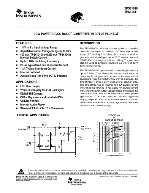
TPS61040中文资料
V O = 18 V200 µS/divFigure 12. Line Transient ResponseV O = 18 V200 µS/div Figure 13. Load Transient ResponseV O = 18 VFigure 14. Start-Up BehaviorIMPORTANT NOTICETexas Instruments Incorporated and its subsidiaries (TI) reserve the right to make corrections, modifications, enhancements, improvements, and other changes to its products and services at any time and to discontinue any product or service without notice. Customers should obtain the latest relevant information before placing orders and should verify that such information is current and complete. All products are sold subject to TI’s terms and conditions of sale supplied at the time of order acknowledgment.TI warrants performance of its hardware products to the specifications applicable at the time of sale in accordance with TI’s standard warranty. Testing and other quality control techniques are used to the extent TI deems necessary to support this warranty. Except where mandated by government requirements, testing of all parameters of each product is not necessarily performed.TI assumes no liability for applications assistance or customer product design. Customers are responsible for their products and applications using TI components. To minimize the risks associated with customer products and applications, customers should provide adequate design and operating safeguards.TI does not warrant or represent that any license, either express or implied, is granted under any TI patent right, copyright, mask work right, or other TI intellectual property right relating to any combination, machine, or process in which TI products or services are used. Information published by TI regarding third–party products or services does not constitute a license from TI to use such products or services or a warranty or endorsement thereof. Use of such information may require a license from a third party under the patents or other intellectual property of the third party, or a license from TI under the patents or other intellectual property of TI.Reproduction of information in TI data books or data sheets is permissible only if reproduction is without alteration and is accompanied by all associated warranties, conditions, limitations, and notices. Reproduction of this information with alteration is an unfair and deceptive business practice. TI is not responsible or liable for such altered documentation.Resale of TI products or services with statements different from or beyond the parameters stated by TI for that product or service voids all express and any implied warranties for the associated TI product or service and is an unfair and deceptive business practice. TI is not responsible or liable for any such statements.Mailing Address:Texas InstrumentsPost Office Box 655303Dallas, Texas 75265Copyright 2002, Texas Instruments Incorporated。
1微型计算机原理与接口技术__课后答案_(邹逢兴_著)_清华大学出版社

2.14 解: (BP)=4433H,(SP)=1022H,
2.15 1. ( CL ) = 0F6H 2. [1E4F6H] = 78H 3. ( BX ) = 0056H , ( AX ) = 1E40H
3
4. ( SI ) = 00F6H , [ SI ] = 0024H 5. ( AX ) = 5678H , [ 09226H ] = 1234H
;'0D’→ CR 键,’0AH’
→ LF 键
;PLUS:正数的个数。
;ZERO: 0 的个数。
DATA
ENDS
;MINUS:负数的个数。
CODE SEGMENT ASSUME CS:CODE,DS:DATA
START: MOV AX,DATA
;给 DS 赋初值,
MOV DS, AX
;建立其数据段的寻址性。
2) 将 ES 段从 EA = 0100H 开始的 128 个字单元清 0。
2.35 解:
MIN: MOV BX, ?1
;3000H
MOV AL, [BX]
MOV CX, ?2
;100H
LP1: INC BX
CMP AL, [BX]
?3 LP2
;JLE
MOV AL, [BX]
LP2: DEC CX
JNZ ?4
MOV MOV XOR NEXT: CMP
CX, 18 SI, 00H BX, BX ARRAY[SI], 00H
JS M_PRO
JZ Z_PRO
P_PRO: INC D_SUM
INC MOV MOV MOV JMP
P_SUM+5 AL, ARRAY[SI] BL, P_SUM+5 (P_ARR-1) [BX], AL NEXT1
(德国E+H)PH测量电极CPS11,CPS11D,CPS41,CPD41D,CPD71,CPS71D,CPF81选型手册(E+H)

请注意过程操 作条件!
测量范围
0...12 pH,-15...80℃ 0...14 pH,0...135℃ 0...10 pH,0...70℃ 1...1 2PH,-15 ...80℃,6ba r,带 盐环 0...1 4pH,0...135℃,16bar, 带离 子捕 捉阱 ,抗中 毒性 强
环境条件
测 量变 量 测 量范 围
环 境温 度 储 存温 度 防 护等 级
Endress + Hauser
输入
pH值 温度
电极类型
AA型电 极 BA型电 极 FA型电 极 AS型电 极 BT型电 极
适用 范围 水/废水 测量 过 程应 用 ,蒸 汽消毒 lg/l浓 度 下的 氢 氟 酸 纯水测量 复杂恶劣介质测量
Endress + Hauser
Orbisint CPS11、CPS11D
CPS11的 设计及 尺寸
机械结构
GSA接头,Pg13.5
EPDM O形圈,带止推环 Ag/AgCl金属引线 “ 改良型Gel” 电解液 Ag/AgCl金属引线
TOP68接头,Pg13.5 EPDM O形圈带止推环
Ag/Ag Cl金属引 线 “改良型Gel”电解液 Ag/AgCl金属引线
TI 079 C/28/ zh/03. 05/(10 .08) 8
Endress + Hauser
Orbisint CPS41和CPS41D
测 量系 统
一 个完整的测 量系 统包 括: ·CPS41 pH电 极或CPS41D数 字 电极 · 变 送 器 ,如Liqu isys M CPM2 23/253(带Memosens 技 术CPS4 1D) · 特 殊 的 测量 电缆 ,如CP K9 或Memosens 数 据电 缆 用 于CPS4 1D · 浸 入 式 ,流 通式 或可 伸 缩 过程 支 架, 如UnifitHC P A4 41
(整理)带通滤波器的设计步骤0001

带通滤波器设计流程滤波器是具有频率选择性的双端口器件。
由于谐振器的频率选择性,所以规定的频率信号能够通过器件,而规定频率信号以外的能量被反射, 从而实现频率选择的功能。
滤波器从物理结构上,就是由一些不同的单个谐振器按相应的耦合系 数组合而成,最后达到规定频率的信号从输出端通过的目的。
1. 滤波器技术指标1.1 工作频率范围: 1060MH ± 100MHz1.2插入损耗: 0.5dB max1.3 驻波比:1.2 max1.4 带外抑制:>20dB@f ± 200MHz >35dB@f ± 300MHz >60dB@f ± 500MHz1.5 寄生通带: f > 3500MHz 以上,对衰减不作要1.6 工作温度:-55 ° Cto+85°C1.7 最大输入脉冲功率:400W最大输入平均功率:20W2. 滤波器设计原理3. 滤波器结构选择3.1物理结构选择根据以上技术指标选择 腔体交指型带通滤波器,主要的原因是因为它 有着良好的带通滤波特性,而且它结构紧凑、结实;且容易制造;谐振杆端口 2图1滤波器原理图的长度近似约为入/ 4(波长)°,故第二通带在3倍fo上,其间不会有寄生响应。
它用较粗谐振杆作自行支撑而不用介质,谐振杆做成圆杆,还可用集总电容加载的方法来减小体积和增加电场强度,而且它适用于各种带宽和各种精度的设计。
3.2电路结构的选择根据以上技术指标选择交指点接触形式,主要的原因是它的谐振杆的一端是开路,一端是短路(即和接地板接连在一起),长约入/ 4 °,载TE M (电磁波)模,杆1到杆n都用作谐振器,同时杆1和杆n也起着阻抗变换作用。
4. 电路仿真设计如图2模型选择。
采用An soft公司的Serenade设计,根据具体的技术指标、体积要求和功率容量的考虑,此滤波器采用腔体交指滤波器类型,使用切比雪夫原型来设计,用圆杆结构的物理方式来实现。
微机原理 期末考试题库及答案(含3套试卷)
微型计算机原理与接口技术综合测试题一一、单项选择题 (下面题只有一个答案是正确的,选择正确答案填入空白处)1.8086CPU通过(1 )控制线来区分是存储器访问,还是I/O访问,当CPU执行IN AL,DX指令时,该信号线为( 2 )电平。
(1) A. M/ B. C. ALE D. N/(2) A. 高 B. 低 C. ECL D. CMOS2.n+1位有符号数x的补码表示范围为()。
A. -2n < x < 2nB. -2n ≤ x ≤ 2n -1C. -2n -1 ≤ x ≤ 2n-1D. -2n < x ≤ 2n3.若要使寄存器AL中的高4位不变,低4位为0,所用指令为()。
A. AND AL, 0FHB. AND AL, 0FOHC. OR AL, 0FHD. OR AL 0FOH4.下列MOV指令中,不正确的指令是()。
A. MOV AX, BXB. MOV AX, [BX]C. MOV AX, CXD. MOV AX, [CX]5.中断指令INT 17H的中断服务程序的入口地址放在中断向量表地址()开始的4个存贮单元内。
A. 00017HB. 00068HC. 0005CHD. 0005EH6.条件转移指令JNE的条件是()。
A. CF=0B. CF=1C. ZF=0D. ZF=17. 在8086/8088 CPU中,一个最基本的总线读写周期由(1 )时钟周期(T状态)组成,在T1状态,CPU往总线上发( 2 )信息。
⑴ A. 1个 B. 2个 C. 4个 D. 6个⑵ A. 数据 B . 地址 C. 状态 D. 其它8. 8086有两种工作模式, 最小模式的特点是( 1 ),最大模式的特点是( 2 )。
⑴ A. CPU提供全部控制信号 B. 由编程进行模式设定C. 不需要8286收发器D. 需要总线控制器8288⑵ A. M/ 引脚可直接引用 B. 由编程进行模式设定C. 需要总线控制器8288D. 适用于单一处理机系统9.在8086微机系统的RAM 存储单元器0000H:002CH开始依次存放23H,0FFH,00H,和0F0H四个字节,该向量对应的中断号是( )。
LMD18201中文资料
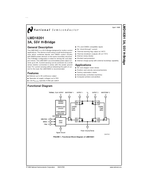
LMD182013A,55V H-BridgeGeneral DescriptionThe LMD18201is a 3A H-Bridge designed for motion control applications.The device is built using a multi-technology pro-cess which combines bipolar and CMOS control circuitry with DMOS power devices on the same monolithic structure.The H-Bridge configuration is ideal for driving DC and step-per motors.The LMD18201accommodates peak output cur-rents up to 6A.Current sensing can be achieved via a small sense resistor connected in series with the power ground lead.For current sensing without disturbing the path of cur-rent to the load,the LMD18200is recommended.Featuresn Delivers up to 3A continuous output n Operates at supply voltages up to 55V n Low R DS(ON)typically 0.33Ωper switchn TTL and CMOS compatible inputs n No “shoot-through”currentn Thermal warning flag output at 145˚C n Thermal shutdown (outputs off)at 170˚C n Internal clamp diodes n Shorted load protectionnInternal charge pump with external bootstrap capabilityApplicationsn DC and stepper motor drivesn Position and velocity servomechanisms n Factory automation robotsn Numerically controlled machinery nComputer printers and plottersFunctional DiagramDS010793-1FIGURE 1.Functional Block Diagram of LMD18201April 1998LMD182013A,55V H-Bridge©1999National Semiconductor Corporation Connection Diagram and Ordering InformationDS010793-2Top ViewOrder Number LMD18201TSee NS Package Number TA11B2Absolute Maximum Ratings(Note1)If Military/Aerospace specified devices are required, please contact the National Semiconductor Sales Office/ Distributors for availability and specifications.Total Supply Voltage(V S,Pin6)60V Voltage at Pins3,4,5and912V Voltage at Bootstrap Pins(Pins1and11)V OUT+16V Peak Output Current(200ms)6A Continuous Output Current(Note2)3A Power Dissipation(Note3)25W Sense Voltage(Pin7to Pin8)+0.5V to−1.0V Power Dissipation(T A=25˚C,Free Air)3W Junction Temperature,T J(max)150˚C ESD Susceptibility(Note4)1500V Storage Temperature,T STG−40˚C to+150˚C Lead Temperature(Soldering,10sec.)300˚COperating Ratings(Note1)Junction Temperature,T J−40˚C to+125˚C V S Supply Voltage+12V to+55VElectrical Characteristics(Note5)The following specifications apply for V S=42V,unless otherwise specified.Boldface limits apply over the entire operating temperature range,−40˚C≤T J≤+125˚C,all other limits are for T A=T J=25˚C.Symbol Parameter Conditions Typ Limit UnitsR DS(ON)Switch ON Resistance Output Current=3A(Note6)0.330.4/0.6Ω(max)R DS(ON)Switch ON Resistance Output Current=6A(Note6)0.330.4/0.6Ω(max)V CLAMP Clamp Diode Forward Drop Clamp Current=3A(Note6) 1.2 1.5V(max)V IL Logic Low Input Voltage Pins3,4,5−0.1V(min)0.8V(max)I IL Logic Low Input Current V IN=−0.1V,Pins=3,4,5−10µA(max)V IH Logic High Input Voltage Pins3,4,52V(min)12V(max)I IL Logic High Input Current V IN=12V,Pins=3,4,510µA(max)Undervoltage Lockout Outputs Turn OFF9V(min)11V(max)T JW Warning Flag Temperature Pin9≤0.8V,I L=2mA145˚CV F(ON)Flag Output Saturation Voltage T J=T JW,I L=2mA0.15VI F(OFF)Flag Output Leakage V F=12V0.210µA(max)T JSD Shutdown Temperature Outputs Turn OFF170˚CI S Quiescent Supply Current All Logic Inputs Low1325mA(max)t D(ON)Output Turn-On Delay Time Sourcing Outputs,I OUT=3A300nsSinking Outputs,I OUT=3A300nst ON Output Turn-On Switching Time Bootstrap Capacitor=10nFSourcing Outputs,I OUT=3A100nsSinking Outputs,I OUT=3A80nst D(OFF)Output Turn-Off Delay Times Sourcing Outputs,I OUT=3A200nsSinking Outputs,I OUT=3A200nst OFF Output Turn-Off Switching Times Bootstrap Capacitor=10nFSourcing Outputs,I OUT=3A75nsSinking Outputs,I OUT=3A70nst PW Minimum Input Pulse Width Pins3,4and51µst CPR Charge Pump Rise Time No Bootstrap Capacitor20µsNote1:Absolute Maximum Ratings indicate limits beyond which damage to the device may occur.DC and AC electrical specifications do not apply when operatingthe device beyond its rated operating conditions.Note2:See Application Information for details regarding current limiting.Note3:The maximum power dissipation must be derated at elevated temperatures and is a function of T J(max),θJA,and T A.The maximum allowable power dissi-pation at any temperature is P D(max)=(T J(max)−T A)/θJA,or the number given in the Absolute Ratings,whichever is lower.The typical thermal resistance from junctionto case(θJC)is1.0˚C/W and from junction to ambient(θJA)is30˚C/W.For guaranteed operation T J(max)=125˚C.Note4:Human-body model,100pF discharged through a1.5kΩresistor.Except Bootstrap pins(pins1and11)which are protected to1000V of ESD.Note5:All limits are100%production tested at25˚C.Temperature extreme limits are guaranteed via correlation using accepted SQC(Statistical Quality Control) methods.All limits are used to calculate AOQL,(Average Outgoing Quality Level).Note6:Output currents are pulsed(t W<2ms,Duty Cycle<5%).3Typical Performance CharacteristicsTest Circuit Switching Time DefinitionsV SAT vs Flag CurrentDS010793-12R DS(ON)vs TemperatureDS010793-13R DS(ON)vsSupply VoltageDS010793-14Supply Current vs Supply VoltageDS010793-15Supply Current vs Frequency (V S =42V)DS010793-16Supply Current vsTemperature (V S =42V)DS010793-17DS010793-8DS010793-9 4Pinout Description(See Connection Diagram)Pin1,BOOTSTRAP1Input:Bootstrap capacitor pin for half H-Bridge number1.The recommended capacitor(10nF)is connected between pins1and2.Pin2,OUTPUT1:Half H-Bridge number1output.Pin3,DIRECTION Input:See Table1.This input controls the direction of current flow between OUTPUT1and OUT-PUT2(pins2and10)and,therefore,the direction of rotation of a motor load.Pin4,BRAKE Input:See Table1.This input is used to brake a motor by effectively shorting its terminals.When braking is desired,this input is taken to a logic high level and it is also necessary to apply logic high to PWM input,pin5. The drivers that short the motor are determined by the logic level at the DIRECTION input(Pin3):with Pin3logic high, both current sourcing output transistors are ON;with Pin3 logic low,both current sinking output transistors are ON.All output transistors can be turned OFF by applying a logic high to Pin4and a logic low to PWM input Pin5;in this case only a small bias current(approximately−1.5mA)exists at each output pin.Pin5,PWM Input:See Table1.How this input(and DIREC-TION input,Pin3)is used is determined by the format of the PWM Signal.Pin6,V S Power SupplyPin7,POWER GROUND/SENSE Connection:This pin is the ground return for the power DMOS transistors of the H-Bridge.The current through the H-Bridge can be sensed by adding a small,0.1Ω,sense resistor from this pin to the power supply ground.Pin8,SIGNAL GROUND:This is the ground return for the internal logic circuitry used to control the PWM switching of the H-Bridge.Pin9,THERMAL FLAG Output:This pin provides the ther-mal warning flag output signal.Pin9becomes active-low at 145˚C(junction temperature).However the chip will not shut itself down until170˚C is reached at the junction.Pin10,OUTPUT2:Half H-Bridge number2output.Pin11,BOOTSTRAP2Input:Bootstrap capacitor pin for half H-Bridge number 2.The recommended capacitor (10nF)is connected between pins10and11.TABLE1.Logic Truth TablePWM Dir Brake Active Output DriversH H L Source1,Sink2H L L Sink1,Source2L X L Source1,Source2H H H Source1,Source2H L H Sink1,Sink2L X H NONEApplication InformationTYPES OF PWM SIGNALSThe LMD18201readily interfaces with different forms of PWM e of the part with two of the more popular forms of PWM is described in the following paragraphs. Simple,locked anti-phase PWM consists of a single,vari-able duty-cycle signal in which is encoded both direction andamplitude information(see Figure2).A50%duty-cyclePWM signal represents zero drive,since the net value ofvoltage(integrated over one period)delivered to the load iszero.For the LMD18201,the PWM signal drives the direc-tion input(pin3)and the PWM input(pin5)is tied to logichigh.Sign/magnitude PWM consists of separate direction(sign)and amplitude(magnitude)signals(see Figure3).The(ab-solute)magnitude signal is duty-cycle modulated,and theabsence of a pulse signal(a continuous logic low level)rep-resents zero drive.Current delivered to the load is propor-tional to pulse width.For the LMD18201,the DIRECTION in-put(pin3)is driven by the sign signal and the PWM input(pin5)is driven by the magnitude signal.USING THE THERMAL WARNING FLAGThe THERMAL FLAG output(pin9)is an open collector tran-sistor.This permits a wired OR connection of thermal warn-ing flag outputs from multiple LMD18201’s,and allows theuser to set the logic high level of the output signal swing tomatch system requirements.This output typically drives theinterrupt input of a system controller.The interrupt serviceroutine would then be designed to take appropriate steps,such as reducing load currents or initiating an orderly systemshutdown.The maximum voltage compliance on the flag pinis12V.SUPPLY BYPASSINGDuring switching transitions the levels of fast currentchanges experienced may cause troublesome voltage tran-sients across system stray inductances.It is normally necessary to bypass the supply rail with a highquality capacitor(s)connected as close as possible to the V SPower Supply(Pin6)and POWER GROUND(Pin7).A1µFhigh-frequency ceramic capacitor is recommended.Careshould be taken to limit the transients on the supply pin be-low the Absolute Maximum Rating of the device.When oper-ating the chip at supply voltages above40V a voltage sup-pressor(transorb)such as P6KE62A is recommended fromDS010793-4FIGURE2.Locked Anti-Phase PWM ControlDS010793-5 FIGURE3.Sign/Magnitude PWM Control 5Application Information(Continued) supply to ground.Typically the ceramic capacitor can be eliminated in the presence of the voltage suppressor.Note that when driving high load currents a greater amount of sup-ply bypass capacitance(in general at least100µF per Amp of load current)is required to absorb the recirculating cur-rents of the inductive loads.CURRENT LIMITINGCurrent limiting protection circuitry has been incorporated into the design of the LMD18201.With any power device it is important to consider the effects of the substantial surge cur-rents through the device that may occur as a result of shorted loads.The protection circuitry monitors the current through the upper transistors and shuts off the power device as quickly as possible in the event of an overload condition (the threshold is set to approximately10A).In a typical motor driving application the most common overload faults arecaused by shorted motor windings and locked rotors.Underthese conditions the inductance of the motor(as well as anyseries inductance in the V CC supply line)serves to reducethe magnitude of a current surge to a safe level for theLMD18201.Once the device is shut down,the control cir-cuitry will periodically try to turn the power device back on.This feature allows the immediate return to normal operationonce the fault condition has been removed.While the faultremains however,the device will cycle in and out of thermalshutdown.This can create voltage transients on the V CCsupply line and therefore proper supply bypassing tech-niques are required.The most severe condition for any power device is a direct,hard-wired(“screwdriver”)long term short from an output toground.This condition can generate a surge of currentthrough the power device on the order of15Amps and re-quire the die and package to dissipate up to500W of powerfor the short time required for the protection circuitry to shutoff the power device.This energy can be destructive,particu-larly at higher operating voltages(>30V)so some precau-tions are in order.Proper heat sink design is essential and itis normally necessary to heat sink the V CC supply pin(pin6)with1square inch of copper on the PC board. INTERNAL CHARGE PUMP AND USE OF BOOTSTRAP CAPACITORSTo turn on the high-side(sourcing)DMOS power devices,the gate of each device must be driven approximately8Vmore positive than the supply voltage.To achieve this an in-ternal charge pump is used to provide the gate drive voltage.As shown in(Figure4),an internal capacitor is alternately switched to ground and charged to about14V,then switched to V S thereby providing a gate drive voltage greater than V S. This switching action is controlled by a continuously running internal300kHz oscillator.The rise time of this drive voltage is typically20µs which is suitable for operating frequencies up to1kHz.For higher switching frequencies,the LMD18201provides for the use of external bootstrap capacitors.The bootstrap principle is in essence a second charge pump whereby a large value capacitor is used which has enough energy to quickly charge the parasitic gate input capacitance of the power device resulting in much faster rise times.The switch-ing action is accomplished by the power switches them-selves(Figure5).External10nF capacitors,connected from the outputs to the bootstrap pins of each high-side switch provide typically less than100ns rise times allowing switch-ing frequencies up to500kHz.INTERNAL PROTECTION DIODESA major consideration when switching current through induc-tive loads is protection of the switching power devices from the large voltage transients that occur.Each of the four switches in the LMD18201have a built-in protection diode to clamp transient voltages exceeding the positive supply or ground to a safe diode voltage drop across the switch. The reverse recovery characteristics of these diodes,once the transient has subsided,is important.These diodes must come out of conduction quickly and the power switches must be able to conduct the additional reverse recovery current of the diodes.The reverse recovery time of the diodes protect-ing the sourcing power devices is typically only70ns with a reverse recovery current of1A when tested with a full3A of forward current through the diode.For the sinking devices the recovery time is typically100ns with4A of reverse cur-rent under the same conditions.DS010793-6FIGURE4.Internal Charge Pump CircuitryDS010793-7FIGURE5.Bootstrap Circuitry6Typical ApplicationsBASIC MOTOR DRIVERThe LMD18201can directly interface to any Sign/Magnitude PWM controller.The LM629is a motion control processor that outputs a Sign/Magnitude PWM signal to coordinate ei-ther positional or velocity control of DC motors.The LMD18201provides fully protected motor driver stage.CURRENT SENSINGIn many motor control applications it is desirable to sense and control the current through the motor.For these types of applications a companion product,the LMD18200,is also available.The LMD18200is identical to the LMD18201but has current sensing transistors that output a current directly proportional to the current conducted by the two upper DMOS power devices to a separate current sense pin.This technique does not require a low valued,power sense resis-tor and does not subtract from the available voltage drive to the motor.To sense the bridge current through the LMD18201requires the addition of a small sense resistor between the power ground/sense pin (Pin 7)and the actual circuit ground (see Figure 7).This resistor should have a value of 0.1Ωor less tostay within the allowable voltage compliance of the sense pin,particularly at higher operating current levels.The volt-age between power ground/sense (Pin 7)and the signal ground (Pin 8)must stay within the range of −1V to +0.5V.In-ternally there is approximately 25Ωbetween pins 7and 8and this resistance will slightly reduce the value of the exter-nal sense resistor.Approximately 70%of the quiescent sup-ply current (10mA)flows out of pin 7.This will cause a slight offset to the voltage across the sense resistor when the bridge is not conducting.During reverse recovery of the in-ternal protection diodes the voltage compliance between pins 7and 8may be exceeded.The duration of these spikes however are only approximately 100ns and do not have enough time or energy to disrupt the operation of the LMD18201.DS010793-10FIGURE 6.Basic Motor DriverDS010793-11FIGURE 7.Current Sensing7Physical Dimensionsinches (millimeters)unless otherwise notedLIFE SUPPORT POLICYNATIONAL’S PRODUCTS ARE NOT AUTHORIZED FOR USE AS CRITICAL COMPONENTS IN LIFE SUPPORT DEVICES OR SYSTEMS WITHOUT THE EXPRESS WRITTEN APPROVAL OF THE PRESIDENT AND GENERAL COUNSEL OF NATIONAL SEMICONDUCTOR CORPORATION.As used herein:1.Life support devices or systems are devices or systems which,(a)are intended for surgical implant into the body,or (b)support or sustain life,and whose failure to perform when properly used in accordance with instructions for use provided in the labeling,can be reasonably expected to result in a significant injury to the user.2.A critical component is any component of a life support device or system whose failure to perform can be reasonably expected to cause the failure of the life support device or system,or to affect its safety or effectiveness.National Semiconductor Corporation AmericasTel:1-800-272-9959Fax:1-800-737-7018Email:support@National Semiconductor EuropeFax:+49(0)180-5308586Email:europe.support@Deutsch Tel:+49(0)180-5308585English Tel:+49(0)180-5327832Français Tel:+49(0)180-5329358Italiano Tel:+49(0)180-5341680National Semiconductor Asia Pacific Customer Response Group Tel:65-2544466Fax:65-2504466Email:sea.support@National Semiconductor Japan Ltd.Tel:81-3-5639-7560Fax:81-3-5639-750711-Lead TO-220Power Package (T)Order Number LMD18201T NS Package Number TA11BL M D 182013A ,55V H -B r i d g eNational does not assume any responsibility for use of any circuitry described,no circuit patent licenses are implied and National reserves the right at any time without notice to change said circuitry and specifications.。
WELL-X1 水箱及 WELL-X1 数字控制器说明书

9013-0006 (03/11)INSTALLER: LEAVE THIS MANUAL WITH THE OWNERThe WELL-X1 tank comes with a 7 year warranty and the WELL-X1 digital control comes with a 2 year warranty. See back page for warranty informationIMPORTANT GENERAL SAFETY INFORMATION - ADDITIONAL SPECIFIC SAFETY ALERTS APPEAR IN THE FOLLOWING INSTRUCTIONS. READ CAREFULLY THE PRODUCT INSTALLATION, OPERATING AND MAINTENANCE MANUAL. FAILURE TO FOLLOW THE INSTRUCTIONS AND WARNINGS IN THE MANUAL MAY RESULT IN SERIOUS OR FATAL INJURY AND/OR PROPERTYDAMAGE, AND WILL VOID THE PRODUCT WARRANTY. THIS PRODUCT MUST BE INSTALLED BY A QUALIFIED PROFESSIONAL. FOLLOW ALL APPLICABLE LOCAL AND STATE CODES AND REGULATIONS, IN THE ABSENCE OF SUCH CODES, FOLLOW THE CURRENT EDITIONS OF THE NATIONAL PLUMBING CODE AND NATIONAL ELECTRIC CODE, AS APPLICABLE.This is the safety alert symbol. It is used to alert you to personal injury hazards. Obey all safety instructions that follow this symbol to reduce the risk of possible injury or death as well as property damage.1400 Division Road, West Warwick, RI 02893 T: 401.884.6300 F: 401.885.2567 1. TABLE OF CONTENTSGENERAL SAFETY INFORMATION ...........................................................2COMPONENTS ............................................................................................3INSTALLATION AND SIZING CONSIDERATIONS .....................................4INSTALLATION CONSIDERATIONS ..........................................................5PLUMBING ..................................................................................................6WIRING ........................................................................................................8STARTUP & ADJUSTMENT ........................................................................9PUMP PROTECTION & DIAGNOSTICS ...................................................13TROUBLESHOOTING ...............................................................................14REPLACEMENT PARTS ...........................................................................15This Product, like most Products under pressure, may over time corrode. weakenand burst or explode, causing serious or fatal injury, leaking or flooding and/or property damage. To minimize risk, a licensed professional must install and periodically inspect and service the Product. A drip pan connected to an adequate drain must be installed if leaking or flooding could cause property damage. Do not locate in an area where leakage of the tank or connections could cause property damage to the area adjacent to the appliance or to lowerfloors of the structure.Chlorine & Aggressive Water: The water quality can significantly influence the life ofthis Product. You should test for corrosive elements, acidity, total solids and other relevant contaminants, including chlorine and treat your water appropriately to insure satisfactory performance and prevent premature failure. NOTE: Inspect for shipping damage and notify freight carrier or store where purchased immediately if damage is present. To avoid risk of personal injury and property damage, if the product appears to be malfunctioning or shows signs of corrosion, call a qualified professional immediately. Current copies of the Product manual can be viewed at . Use proper safety equipment when installing.ELECTROCUTION AND EXPLOSION HAZARD! Before work is performed on the Product, turn off the power to theProduct and release all pressure in the system.As in all plumbing products and water storage vessels, bacteria can grow in this Product, especially during times of non-use. Consult yourlocal plumbing professional regarding any steps you mayplumbing system.DANGER! EXPLOSION HAZARD , WHENTHE WELL-X1®HAS BEEN IN SERVICEAND A CHANGE TO A HIGHER PRE-CHARGE PRESSURE IS NECESSARY DUE TO A REQUIRED CHANGE IN THE PRESSURE SWITCH SETTING, FAILURE TO FOLLOW INSTRUCTION MANUAL CAN CAUSE A RUPTURE OR EXPLOSION, POSSIBLY CAUSING SERIOUS OR FATAL INJURY , AND/OR PROPERTY DAMAGE. • DO NOT ADJUST THE PRE-CHARGE PRESSURE IF THERE HAS BEEN AREDUCTION OF THE PUMP CYCLE TIME OR THE PRE-CHARGE PRESSURE COMPARED TO ITS INITIAL SETTING. THIS IS BECAUSE REDUCTION IN PUMP CYCLE TIME CAN RESULT FROM LOSS OF TANK AIR PRESSURE WHICH IN TURN CAN MEAN THERE MAY BE INTERNAL CORROSION AND ANY RE-PRESSURIZATION OR ADDITIONAL PRESSURE COULD RESULT IN RUPTURE OR EXPLOSION, AND/OR PROPERTY DAMAGE.RELIEF VALVE REQUIRED . A relief valve has been installed which is set to open atexcessive pressures (100 psig or more). This will protect the Well-X1® and other system components should the pressure switch malfunction and fail to shut the pump off. The relief valve is installed at the connection of the Well-X1® to the system piping.Before attempting any service and disassembly, shut off power to the pump.Ensure power is disconnected prior to removing motor. Ensure power is disconnected before cleaning is attempted.This control is capable of running pumps to pressures that may exceed thelimitations of system components. Never set the operation pressure higher than that of the safe system capacity.This control can be adjusted to a narrow pressure differential. This can cause thepump to cycle rapidly with an improperly sized tank, leadingto pump damage. This may require a larger pressure tank than normally used.Every Well-X1® is air tested to 150 psig, the maximum working pressure for the Well-X1®.The pump controller is not a disconnect. The pump may be activated at any time.The electrical system must be considered energized at all times unless the circuit breaker is open. The disconnect for the controller must break all incoming power lines. As with a mechanical pressure switch, when installed with three wire 230 vac pumps or any 3-phase pump, a standard pump motor starter or a relay must be used.2. GENERAL SAFETY INFORMATION3. COMPONENTSThe Well-X1® combines all the standard well tank components in a single, easy to install package. The pressure tank, control and tank fittings are factory-installed. After removing from the carton, inspect the Well-X1 for damage and ensure all components are present.CONTROLPRESSURE TANKMOUNTING BRACKET4. INSTALLATION AND SIZING CONSIDERATIONSThe Well-X1® functions like a traditional pressure switch by cycling the pump on and off. The factory pressure settings are 40 psi cut-in and 60 psi cut-out. The controller allows these settings to be adjusted to best suit the application. The Well-X1® can operate in two primary modes:A. STANDARD OPERATIONUsing a standard 20 psi differential, the Well-X1® can be sized according to the chart below. In this application, the sizing and performance will be similar to a traditional pressure tank and mechanical switch combination.B. CONSTANT PRESSURE MODEThe Well-X1® control allows a narrow differential to provide consistent water pressure. The factory 20 psi differential can be reduced so the cut-in and cut-out pressures are within 10 psi. When installed as a constant pressure system, the chart below should be used to ensure the tank volume is sufficient to provide adequate cycle protection.A relief valve has been installed which is set to open at excessive pressures (100 psig or5. INSTALLATION CONSIDERATIONS LOCATIONThe Well-X1® is designed for indoor and outdoor installations. The NEMA 3 enclosure can be installed in direct weather. If installed outdoors, be sure the following conditions are met:• Do not install where ambient temperatures can drop below freezingor exceed 120° F.• Use water-tight: wiring conduit, wire nuts and conduit connectionsas dictated by applicable codes and ordinances.• Protect the piping from mechanical damage.• Install the relief valve blow down tube where venting water will notcause personal injury or damage the surrounding property.• Drip Pan and Drain: To avoid leaking and/or property damage,install with a drip pan connected to an adequate working drain keptclear at all times.ORIENTATIONEnsure the installation meets all applicable local codes and is installed by a qualified professional. Additionally, the following should be noted.• This unit is designed for vertical installation above ground only.Do not install horizontally or directly bury the unit. The Well-X1®may be installed below grade in a well pit or other suitableenclosure. Do not locate in an area where leaking or floodingcould cause property damage to surrounding areas.• Check codes to determine if there are any height requirementspertaining to the Well-X1®. Particularly, ensure the bottomdrain meets these requirements. If restrictions are imposed onthe proximity of drain connections to the floor, the unit may beelevated on blocks or the bottom drain tube can be removed andplugged, after which a sampling tap may be installed in the waterlines near the top of the Well-X1®.6. PLUMBING 1. Plumbing connections are similar to a traditional "tankcross" or "tank tee". Provisions are made for popular linesizes via a 1-1/4" NPT male outer thread and a 1" NPTfemale inner thread. The plumbing connections are notdirectional and allow flow from either side. When attachingvalves or fittings, uses the wrench flats provided.EXPLOSION HAZARD. Failure tofollow these instructions can cause a rupture or explosion possibly causing serious or fatal injury, flooding, and/or property damage.2. Install the supply piping from the well pump. If required, install a spring-loaded check valve.3. Install a shutoff (service) valve on the outgoing line. This will allow the Well-X1® to be tested prior to pressurizing the entire system. DO NOT place a shutoff on the incoming supply line.NOTE: The relief valve is sized for a maximum flow rate of 10 gpm at 125 psi. If the pump installation allows higherflow rates, an additional relief valve must be installed.4. Connect the water line from the well pump to the inlet of the Well-X1®.5. Plumb the outgoing supply to the building's water supply system or into the water treatment equipment (if present).6. Install a blow down tube from the relief valve to a drainor to within 6" of the floor as required by local codes.A drip pan connected to an adequate drain must be installed if leaking orflooding could cause property damage.7. WIRING 1. Shut off the circuit breaker for the well system. Loosenthe silver screw on top of the control and remove coverto expose the control wires.Electrocution hazard. For your safety, minimize the risk of electric shock, property damageor personal injury. Properly ground to conform with all governing codes and ordinances.2. The 12 gauge wire leads are pre-stripped and readyto accept standard wire nuts. Each wire is color codedto correspond with the diagram below. Use water tight conduit, connections, and wire nuts for an outside application.3. Wiring is similar to a traditional mechanical pressure switch. Two leads are connected to line supply, while the other supply the pump motor or starter. Wire the control to the line supply and pump motor or pump starter as required by the manufacturer's instructions. It is recommended that service switch be installed in addition to the circuit breaker. The disconnect for the controller must break all incoming power lines. This should interrupt line voltage and be installed near the Well-X1® and labeled appropriately.4. After completing the wiring, reattach top cover and tighten screw. Ensure no loose wires protrude from the control.L LMOTOMOTOBLACKWHITE/STRIPEBLUEWHITESCREW8. STARTUP & ADJUSTMENT1. After plumbing and wiring are complete, close the service valve to allow startup without pressurizing the entire plumbing system. If a service valve was not installed, close all fixtures in the home. Ensure the bottom drain is closed.2. Restore power to the Well-X1® by turning on the breaker and electrical service switch (if installed). The display will illuminate.3. The display will read "88" to test the display illumination, then a number identifying the control type (i.e. 15). This number is for factory use and may vary by model and manufacture date.4. After a slight pause, the pump will start and the system pressure will be displayed. This number will increase as the pump runs and the tank fills.Note: Some jet pumps may be difficult to prime, resulting in the low water cut-off activating if pressure will not build above 10 psig. Depressing the s arrow will temporarily override the low water cut-off to allowproper priming.8. STARTUP & ADJUSTMENT (con't)5.The factory cut-out (pump off) setting is 60 psig. When the pump reaches 60 psig, the Well-X1® will shut the pump off. Check the plumbing for leaks and repair before continuing. If during startup the cut-out setting of 60 psig cannot be reached, read the adjustment instructions to lower the cut-out within the pump's capability.6. Slowly open the service valve to allow the system to pressurize. The pressure may drop slightly during this process. After the valve is fully open, open the fixture closest to the Well-X1® to begin drawing water from the tank.7. When the system reaches the factory cut-in (pump on) setting of 40 psig, the pump will start. Like a traditional mechanical switch, the pressure will begin to rise, repeating the cycle. If desired, the Well-X1® settingscan now be adjusted as shown below.1. To enter the programming mode, press and hold the ■ button until LO appears. This is the cut-in setting. Factory default will be 40 psi.2. Use the s and t arrows to raise or lower the cut-in setting. Adjustment can be made within 10 psig or as wide as 55 psig of the cut-out setting to 60 psig. If this range is exceeded, the display will cease to change even though the button is being pressed. Minimum setting is 10 psig.PRESSURE ADJUSTMENTThe Well-X1® utilizes a simple cut-in/cut-out adjustment. Before setting the desired operating range, refer to the chart below to ensure the Well-X1's Maximum Acceptance is not exceeded. Adjust the precharge as shown on page 12.CAUTION!Exceeding Maximum Acceptance will reduce tank life and cause irreparable damage.Step 1: Find the Maximum Acceptance for the installed Well-X1® model.Step 2: Ensure the desired operating range does notexceed that model's Maximum Acceptance.3. To adjust the cut-out, depress ■ once and the display will read HI . Again, press the t or s buttons to raise or lower the setting. The same 10-55 psig differential range applies.Maximum setting is 80 psig.4. A fter adjusting the cut-in and cut-out, release the buttons. After a slight pause, Pr will be displayed, indicating the settings are saved in the event of a power outage.PRECHARGE ADJUSTMENTWhenever the cut-in (LO) setting is changed, the tank precharge must be adjusted. To do this, shut the Well-X1® off and open the drain to empty all water. Using an air gauge, adjust the precharge to 2 psig below the cut-in (LO) setting.Failure to adjust the precharge will result in tank damageor water interruption.DANGER! Explosion Hazard. If theWell-X1®has been in service and a change to a higher pre-charge is necessary due to a required change in the setting, failure to follow instruction below can cause a rupture or explosion, possibly causing serious or fatal personal injury, and/or property damage.• Do not adjust or add pressure if there has been a loss of air.• Do not adjust the pre-charge pressure if there is visible exterior corrosion.• Do not adjust the pre-charge pressure if there has been a reduction in pump cycle time or the pre-charge pressure compared to its initial setting. This is because reduction in pump cycle time can result from loss of tank air pressure which in turn can mean there may be internal corrosion and any re-pressurization or additional pressure could result in rupture or explosion.9. PUMP PROTECTION AND DIAGNOSTICSThe Well-X1® continually monitors pressure, cycle time and voltage to protect the well pump. The following error codes alert the user to a potential problem, prompting service.E1: Rapid CycleE2: Low Suction (low water cut-off)E3: Voltage ProtectionWELL-X1® ERROR CODESWhen an error occurs, the display will flash a diagnostic code.10. TROUBLESHOOTING11. REPLACEMENT PARTS328AMTROL, AMTROL logo, GUARDIAN CP and Well-X1 are registered trademarks of AMTROL Inc. and affiliatesin the U.S. and elsewhere. All rights reserved.Revised 01/111400 Division Road, West Warwick, RI 02893 T: 401.884.6300 F: 401.885.2567 。
74LVC1G74DC-G中文资料

2 of 20
NXP Semiconductors
74LVC1G74
Single D-type flip-flop with set and reset; positive edge trigger
C
C C
D
C RD
SD
CP
C
C
Fig 3. Logic diagram
6. Pinning information
plastic extremely thin small outline package; no leads; SOT996-2 8 terminals; UTLP based; body 3 × 2 × 0.5 mm
plastic extremely thin quad flat package; no leads; 8 terminals; UTLP based; body 1.6 × 1.6 × 0.5 mm
模块一 行列式

10)行列式的按行或列的展开
∑a A
k =1 ki
n
kj
= Dδ
ij
∑a A
k =1 ik
n
jk
= Dδ
ij
D ,当 i = j; = 按行展开 0 , 当 i ≠ j .
例4:设
D=
1 2 3 4
2 3 4 1
3 4 1 2
4 1 2 3
则
(1) A12 + 2 A22 + 3 A32 + 4 A42 = (
例5:已知A是m阶矩阵,B是n阶矩阵,则m+n阶 行列式
* A B O
m+n
的值是( )
( A ) | A || B | ( C )( − 1) | A || B |
( B ) − | A || B | ( D ) ( − 1)
mn
| A || B |
解:用列交换将此行列式变为分块行列式的形 式。为使A和B内部结构不变,可将A的各列(自 左到右)作相邻两列的交换,共需作mn次,可把 原行列式化为
将第一列加 到第二、 三、四列上
− 1 0 0 −5 − 1 0 −5 0 = 15 −1 −5 0 0 −1 0 0 0
按第四行 展开
0 0 −5 = 15 0 −5 0 −5 0 0
= 1875
方法三:化为三角行列式 例2 计算 x a1 D n + 1 = a1 L a1 a1 x a2 L a2 a2 x L a3 a3 a3 L a4 L L L L L an an an . L x
A特征值为0, 0 ,0 ,4 B特征值(x-1)(三重值),(x+3)
|B|= (x-1)3(x+3) x1,2,3=1, x=3
无细胞体外表达:方法和应用

• TNT® T3 Coupled Reticulocyte Lysate System (L4950) • TNT® T7/T3 Coupled Reticulocyte Lysate System (L5010) • TNT® T7/SP6 Coupled Reticulocyte Lysate System (L5020)
oo
oo
ooo ooo
UUU
O NC
N OC
S NO N
加入进无细胞 翻译体系中
mRNA
21
O CN
ON S N
N CO
ε N
OC
C
O
NαH3
OC N
O NN S
NC O
CO εN
O NHα3 C
C O NHα3
εN CO
N OC
O NC
S NN O
新生肽链
NH3
三种标记方法来源
• 同位素标记的氨基酸
8
复习:转录
• 原核RNA 聚合酶:全酶= 核心酶(α2ββ’)+ σ因子 真核mRNA转录酶: RNA聚合酶 II
• 转录可分成3个阶段
起始 启动子(真核可能有保守的TATA Box,原核Pribnow)) 延伸 终止 l 真核mRNA的转录后加工
l 5‘端形成帽子结构(m7GpppGp-) l 3‘端加上多聚腺苷酸尾巴(polyA tail)
第二章 矩阵及其运算 《工程数学线性代数》课件PPT

0
x
§2 矩阵的运算
例 某工厂生产四种货物,它在上半年和下半年向三家商店 发送货物的数量可用数表表示:
a11 a12 a13 a14 a21 a22 a23 a24 a31 a32 a33 a34
其中aij 表示上半年工厂向第 i 家 商店发送第 j 种货物的数量.
c11 c12 c13 c14 c21 c22 c23 c24 c31 c32 c33 c34
行数不等于列数 共有m×n个元素 本质上就是一个数表
det(aij )
(aij )mn
三、特殊的矩阵
1. 行数与列数都等于 n 的矩阵,称为 n 阶方阵.可记作 An.
2. 只有一行的矩阵 A (a1, a2 ,L , an ) 称为行矩阵(或行向量) .
a1
只有一列的矩阵
B
a2
M
称为列矩阵(或列向量)
说明:只有当两个矩阵是同型矩阵时,才能进行加法运算.
知识点比较
a11 a12 a13 a11 b12 a13 a11 a12 b12 a13 a21 a22 a23 a21 b22 a23 a21 a22 b22 a23 a31 a32 a33 a31 b32 a33 a31 a32 b32 a33
( )A A A (A B) A B
备 注
矩阵相加与数乘矩阵合起来,统称为矩阵的线性运算.
知识点比较
a11 a12 a13 a11 a12 a13 a11 a12 a13 a21 a22 a23 a21 a22 a23 a21 a22 a23
a31 a32 a33 a31 a32 a33 a31 a32 a33
a12 a22
a13 a23
a14 a24
《线性代数与空间解析几何》哈工大版课件幻灯和习题.ppt

3 1
10.
1
2、
3
2
1
1
2
3 1 3 2 3 2 1 2 2
11 12
33 23
3 2
13 1
6 4 2
9
6 3
3、
b1
b2
b3
a11 a21
a12 a22
a13 b1 a23 b2
a31 a32 a33 b3
=( a11b1 a21b2 a31b3
a12b1 a22b2 a32b3
例3 设 A 1 1 B 1 1 1 1 1 1
则 AB 0 0, BA 2 2 ,
0 0
2 2
故 AB BA.
但也有例外,比如设
A 2 0, 0 2
B 1 1, 1 1
则有 AB 2 2, 2 2
BA 2 2
2 2 AB BA. 此时称矩阵A、B可交换。
An2 A
aann11Ana1n2 an2 Aann2n A1n aAnn2nAnn AAnn
A
O
O
A
A
, A
故 AA A E.
同理可得
A
A
n k 1
Aki akj
A E.
五、小结
加法
数与矩阵相乘
矩 阵
矩阵与矩阵相乘
运 转置矩阵
算 方阵的行列式
对称阵与伴随矩阵 共轭矩阵
与反对称阵之和.
证明 设C A AT
则CT
A AT
T
AT
A
C,
所以C为对称矩阵.
设B A AT , 则BT A AT T AT A B,
所以B为反对称矩阵.
GaN- Processing, defects, and devices

APPLIED PHYSICS REVIEWSGaN:Processing,defects,and devicesS.J.Pearton a)Department of Materials Science and Engineering,University of Florida,Gainesville,Florida32611J.C.ZolperOffice of Naval Research,Arlington,Virginia22217R.J.ShulSandia National Laboratories,Albuquerque,New Mexico87185F.RenDepartment of Chemical Engineering,University of Florida,Gainesville,Florida32611͑Received16October1998;accepted for publication3March1999͒The role of extended and point defects,and key impurities such as C,O,and H,on the electrical and optical properties of GaN is reviewed.Recent progress in the development of high reliability contacts,thermal processing,dry and wet etching techniques,implantation doping and isolation,and gate insulator technology is detailed.Finally,the performance of GaN-based electronic and photonic devices such asfield effect transistors,UV detectors,laser diodes,and light-emitting diodes is covered,along with the influence of process-induced or grown-in defects and impurities on the device physics.͓S0021-8979͑99͒00613-1͔TABLE OF CONTENTSI.Introduction (1)II.Processing (2)A.Ohmic and Schottky contacts (2)B.Rapid thermal processing (6)C.Gate dielectrics (22)D.Wet etching (24)E.Dry etching (28)F.Implant isolation (39)III.Role of Impurities (40)A.Hydrogen (40)B.Oxygen (54)C.Carbon (56)IV.Devices (57)A.AlGaN/GaN Electronics (57)B.Ultrahigh power switches (64)ser diodes (66)D.Light-emitting diodes (67)E.UV Photodetectors (68)V.Summary (69)References (69)I.INTRODUCTIONCurrent GaN-based device technologies include light-emitting diodes͑LEDs͒,laser diodes,and UV detectors on the photonic side and microwave power and ultrahigh power switches on the electronics side.1The LED technology is by now relatively mature,with lifetimes of blue and green emit-ters apparently determined mostly by light-induced degrada-tion of the polymer package that encapsulates the devices.2 The main trends in this technology appear to be optimization of optical output efficiency and solving the polymer package degradation issue.For the laser diodes one of the main life-time limiters is p-ohmic contact metal migration along dis-locations which short out the GaN p-contact layer by spiking all the way to the n side of the junction.3,4This is exacer-bated by the generally high specific contact resistance(R C) of the p-ohmic contact and the associated heating of this area during device operation.The advent of lower threshold de-vices and dislocation-free GaN overgrowth of SiO2-masked regions has allowed achievement of laser lifetimes over 10000h.5Facet formation on the laser has been achieved by dry etching,cleaving,polishing,and selective/crystallo-graphic growth.In structures grown on Al2O3both contacts must be made on the top of the device and hence dry etching is necessary to expose the n side of the junction.Fabrication of UV detectors is relatively straightforward and the main issue seems to be one of improving material purity and quality.With respect to electronic devices for microwave power applications,the main process improvements needed are in the areas of low R C n-ohmic contacts͑the requirements are more stringent than for photonic devices,with R C р10Ϫ7⍀cmϪ2being desirable͒,stable and reproducible Schottky contacts,and low damage dry etching that main-tains surface stoichiometry.For the proposed high power switches͑capable of25kA with3kV-voltage standoff͒there are a number of possible device structures,including thyris-a͒Electronic mail:spear@mse.ufl.eduJOURNAL OF APPLIED PHYSICS VOLUME86,NUMBER11JULY19991tors and several types of power metal-oxide-semiconductor field-effect transistor ͑MOSFET ͒.A schematic of a lateral GaN MOSFET is shown in Fig.1.In this case,critical tech-nologies include high implant activation efficiency,gate in-sulator,trench etching for capacitor formation,and stable high temperature/high current stable ohmic contacts.Recent progress in the development of dry and wet etch-ing techniques,implant doping and isolation,thermal pro-cessing,gate insulator technology,and high reliability con-tacts is first reviewed.Etch selectivities up to 10for InN over AlN are possible in inductively coupled plasmas using a Cl 2/Ar chemistry,but in general selectivities for each binary nitride relative to each other are low ͑р2͒because of the high ion energies required to initiate etching.Improved n -type ohmic contact resistances are obtained by selective area Si ϩimplantation followed by very high temperature ͑Ͼ1300°C ͒anneals to minimize the thermal budget and AlN encapsulation which prevents GaN surface decomposition.Implant isolation is effective in GaN,AlGaN,and AlInN,but marginal in InGaN.Candidate gate insulators for GaN in-clude AlN,AlON,and Ga ͑Gd ͒O x ,but interface state densi-ties must still be decreased to realize state-of-the-art metal-insulator-semiconductor ͑MIS ͒devices.Many outstanding reviews on GaN materials and devices have appeared previously,6–14so we will focus on processing and the influence of defects and impurities on devices.II.PROCESSINGA.Ohmic and Schottky contacts1.Schottky contactsThere are still large variations in barrier heights reported by different workers for standard metals on GaN.Pt appears to produce the highest consistent values ͑ϳ1.0–1.1eV ͒with Ti producing the lowest ͑0.1–0.6eV ͒.The variability ap-pears to result from the presence of several transport mecha-nisms,and to materials and process factors such as defects present in these films,the effectiveness of surface cleans prior to metal deposition,local stoichiometry variations,and variations in surface roughness which could affect unifor-mity of the results.New work on silicides showspromise.15,16For Schottky contacts Pt appeared to be stable to approximately 400°C for 1h,while PtSi is somewhat more stable ͑500°C,1h ͒,and also has barrier heights of ϳ0.8eV.Recent reviews and studies of Schottky contact proper-ties on GaN have appeared.15–28The measured barrier heights in most cases are a function of the difference be-tween the metal work function and the electron affinity of GaN.Some typical values for barrier height for different metals are 1.1eV for Pt,190.91–1.15eV for Au,20,210.6eV for Ti,22and 0.94eV for Pd.23For Ni there is a fairly large discrepancy in reported values,ranging from 0.6624to 0.99eV.25For deposition onto n -GaN (ϳ1017cm Ϫ3),rectifying behavior was observed for Pt,Ni,Pd,Au,Co,Cu,Ag,ohmic behavior for So,Hf,Zn,Al,and V,while intermediate be-havior ͑slightly rectifying ͒was obtained for Nb,Ti,Cr,W,and Mo.16Schmitz et al.16calculated from their data that the density of surface states on GaN was ϳ1.8ϫ1013cm Ϫ2eV Ϫ1,suggesting the degree of pinning of the barrier height is less than GaAs where the surface state den-sity is roughly an order of magnitude higher.A comparison of barrier height data from various sources is shown in Fig.2.16,29–33In the early days of form-ing rectifying contacts on GaN it was often believed the Fermi level at the surface and at the metal–nitrides interface was unpinned.The data of Fig.2shows that indeed the bar-rier height does vary with metal work function.The strategy is then to use a metal with a large work function on GaN ͑such as Pt ͒to form a Schottky barrier,while a metal with a low work function ͑such as Ti ͒should be selected for ohmic contacts.The influence of the surface cleanliness is obviously most important in determining the quality of the Schottky contact.In situ deposition of Ga,followed by thermal desorption under ultrahigh vacuum conditions is found to produce clean GaN surfaces,34,35while in situ N 2ϩionsputtering can also remove native oxides.36,37Liu and Lau 15,FIG. 1.Schematic of an ultra high breakdown voltage GaN powerMOSFET.pilation of published results for Schottky barrier heights on GaN ͑after Refs.18,28,and 68͒.Liu et al.,38and Mohney and Lau18have reviewed surfacecleaning processes for GaN.A number of different acid so-lutions,including HNO3/HCl,HCl/H2O,and HF/H2O,havebeen examined for removing the native oxide,39and superiorcurrent–voltage characteristics are observed for the resultantrectifying contacts.40As with other III–V compound semi-conductors,HCl and HF can significantly reduce the oxideon GaN,41,42while the bases NH4OH and NaOH can alsodissolve the oxide.43To this point,there has been no cleardemonstration of the effect of the polarity of the epilayer onthe barrier height.Mohney and Lau18have also commented on the fact thatthere can be significant spatial differences in the quality ofSchottky barrier contacts on a n-GaN,with diodes showingideality factors ranging fromϽ1.1toу1.3on the same wa-fer.While thermionic emission is clearly the dominant cur-rent transport mechanism in most diodes,tunneling and gen-eration recombination may also be present.In many casesthe high dislocation density in material used to date are prob-ably responsible for most of the spatial variations.The thermal stability of Schottky contacts on GaN iscritically important for practical device operation.The ther-mal limits of most of the metal/GaN combinations are be-tween300and600°C,specifically300°C for Pd,44400°Cfor Pt,45575°C for Au,46and600°C for Ni.18As mentionedearlier,the silicides of Pt and Ni display greater thermalstability than the pure metals.45These contacts however maynot be in thermodynamic equilibrium with the GaN,leadingto the formation of metal gallides and silicon nitride uponprolonged annealing.There is little information on barrier heights on p-GaNdue to the general difficulty in growing high quality p-typematerial and the low hole mobility.A barrier height of2.38eV was reported for Au on p-GaN.472.n-ohmic contactsThe commonly accepted ohmic contact to n-GaN is Ti/Al,which is generally annealed to produce oxide reductionon the GaN surface.Multilevel Au/Ni/Al/Ti structures ap-pear to give wider process windows,by reducing oxidationof the Ti layer.48R C values ofр10Ϫ5⍀cm2have been pro-duced on heterostructurefield-effect transistor͑HFET͒de-vices using Ti/Al annealed at900°C for20s.15Both W and WSi x on nϩepi-GaN layers(n ϳ1019cmϪ3)produce reasonable contacts(R Cϳ8ϫ10Ϫ5⍀cm2),but extremely stable behavior49—annealing at1000°C led to shallow reacted regions ofр100Å,and in junctionfield-effect transistor structures these contacts can withstand implant activation anneals at1100°C.50Reaction with the GaN is relatively limited,although-W2N interfa-cial phases are found after800°C anneals,and this appears to be a barrier to Ga out-diffusion.49By contrast to the n-metal systems,the standard p-ohmiccontact to GaN is Ni–Au,with R C valuesу10Ϫ2⍀cm2. Efforts tofind a superior alternative have proved fruitless to date,51even though strong efforts have been made on multi-component alloyed contacts where one attempts to extract one of the lattice elements,replace it with an acceptor dop-ant,and simultaneously reduce the‘‘balling-up’’of the met-allization during this reaction.The model system for thistype of contact is AuGeNi/n-GaAs.A promising approach isto reduce the band gap through use of p-type InGaN on thetop of the GaN.To date there have been reports of achievingp-doping(ϳ1017cmϪ3)in compositions up toϳ15%In.The III nitrides pose a problem however,in the develop-ment of low resistance ohmic contacts because of their wideband gaps.Most of the work done in the area has been fo-cused on n-type GaN.Au and Al single metal contacts tonϩGaN and nonalloyed Au/Ti and Al/Ti were found to havecontact resistances ofϳ10Ϫ3to10Ϫ4⍀cm2.46,52–58Al-containing contacts perform best when oxidation is mini-mized.Lin et al.59reported the lowest contact resistance tonϩGaN,with Ti/Al contacts after annealing at900°C for30s in a rapid thermal annealer(R Cϭ8ϫ10Ϫ6⍀cm2).They suggested the formation of a TiN interface as important in the formation of the low resistance contact.Most of the tran-sition metal elements,including Ti,V,and Sc react with GaN to form nitrides,gallides,and metal–Ga–N ternary phases.18Thermodynamic calculation indicate that the met-als themselves are not in equilibrium with GaN under normal processing conditions,with the consequent probability of in-terfacial reactions occurring.60Both Ti and TiN have been shown to produce ohmic contacts on n-GaN,61,62with Ti consuming GaN during reaction͑a few hundred angstroms at ϳ1000°C for30s͒to form TiN.63Three phase equilibria for the Ti–Ga–N͑and V–Ga–N and Cr–Ga–N͒systems at 800°C have been reported by several groups.64–66The an-nealing ambient plays a strong role,since if the N2partial pressure is greater than that in equilibrium with a metal/GaN contact during reaction,there is a driving force to incorpo-rate nitrogen from the gas phase.18Moreover,there is quite different behavior observed for deposited TiN/GaN contacts relative to those formed by reaction of Ti with GaN in a N2 ambient.In the former case,thermionic emission appears to be the dominant conduction mechanism whereas in the latter tunneling seems to be most important.18Modification of the GaN surface by high temperatureannealing67or reactive ion etching48,68to produce preferen-tial loss of N2can improve n-type ohmic contact resistanceby increasing electron concentration in the near-surface re-gion.Many other metals can be employed to form bilayer Al/metal/GaN n-ohmic contacts,including Pd,69,70Ta,71Nd,72Sc,18and Hf.18All of these form good ohmic contacts,withspecific contact resistances in the10Ϫ5⍀cm2range.A particularly attractive method for reducing R C on de-vice structures is self-aligned implantation of Siϩto heavilydope source/drain ohmic contact regions.This approach hasbeen employed to achieve high quality contacts on hetero-structurefield-effect transistor͑HFET͒structures.73W wasfound to produce low resistance ohmic contacts to nϩGaN(R Cϭ8ϫ10Ϫ6⍀cm2)with little interaction between the semiconductor and the metal up to800°C.49WSi x on nϩGaN was found to be stable to800°C as well,with a contact resistance ofϳ10Ϫ5⍀cm2.Graded contact layers to GaN have been formed with both InN74and InGaN using WSi x metallization.Nonalloyed Ti/Pt/Au on InN produced specific contact resistance R Cϭ1.8ϫ10Ϫ7⍀cm2.74GradedIn x Ga1Ϫx As/InN contacts have been employed on GaAs/ AlGaAs heterojunction bipolar transistors,with R C as low as 5ϫ10Ϫ7⍀cm2.75For high temperature electronics applications,or for high reliability,it would be preferable to employ refractory metal contacts such as W and WSi x.Moreover,the contact resis-tance could be reduced if lower band gap In-containing al-loys͑or InN͒were used as contact layers on GaN,much as in the case of InGaAs on GaAs.However,the In-based nitrides are less thermally stable than GaN,and we need to establish the trade off between contact resistance and poorer tempera-ture stability.Recent experiments on formation of W,WSi0.44and Ti/Al contacts deposited on nϩIn0.65Ga0.35N(n ϳ1020cmϪ3),nϩInN(nϳ1020cmϪ3),and nϪIn0.75Al0.25N (nϳ1018cmϪ3)have been reported.74,75The electrical, structural,and chemical stability of these contacts were ex-amined after anneals up to900°C.It was found that InGaN allows achievement of excellent contact resistance (Ͻ10Ϫ6⍀cm2),with stability up toϳ600°C for W metal-lization.The2000-Å-thick InGaN,InN,and InAlN samples weregrown using metal organic molecular beam epitaxy ͑MOMBE͒on semi-insulating,͑100͒GaAs substrates in an Intevac Gen II system as described previously.76,77The InN,In0.65Ga0.35N,and In0.75Al0.25N were highly autodoped n type(ϳ1020,ϳ1019,and8ϫ1018cmϪ3,respectively͒due to thepresence of native defects.The samples were rinsed in H2O:NH4OH͑20:1͒for1min just prior to deposition of the metal to remove nativeoxides.The metal contacts were sputter deposited to a thick-ness of1000Åin the case of W and WSi0.44͑film composi-tion͒,and then etched in SF6/Ar in a plasma-therm reactive ion etcher͑RIE͒to create transmission line method͑TLM͒patterns.For the Ti/Al contacts,200Åof Ti and then1000Åof Al was deposited and the TLM pattern formed by lift-off of the resist mask.The nitride samples were subsequently etched in Cl2/CH4/H2/Ar in an electron cyclotron resonance ͑ECR͒etcher to produce the mesas for the TLM patterns.78 The samples were annealed at temperatures from300to 900°C for15s under a nitrogen ambient in a rapid thermal annealing͑RTA͒system͑AG-410͒.The contact resistance for W,WSi x,and Ti/Al ohmiccontacts to InGaN as a function of annealing temperature isshown in Fig.3.All contacts had similar contact resistanceas deposited,2–4ϫ10Ϫ7⍀cmϪ2.Above600°C,the Ti/Al contacts degraded rapidly,and the WSi x continued to de-grade,while R C for both samples increased up to ϳ10Ϫ5⍀cm2at900°C.The error in these measurements was estimated to beϮ10%due mainly to geometrical con-tact size effects.The widths of the TLM pattern spacings varied slightly due to processing͑maximum ofϮ5%͒as de-termined by scanning electron microscopy͑SEM͒measure-ments,which were taken into account when calculating the contact resistances.SEM micrographs of W and Ti/Al contacts on InGaN asgrown and annealed showed the W was still quite smootheven after900°C anneal,while the Ti/Al had significant pit-ting at the lowest anneal of500°C even though the contact resistance did not degrade untilу600°C.Auger electron spectroscopy͑AES͒showed that the degradation was due to out-diffusion of In and N.The contact resistance for ohmic contacts of W,WSi x, and Ti/Al to InN as a function of annealing temperature is shown in Fig.4.As-deposited samples had similar contact resistances to InGaN,indicating a similar conduction mecha-nism.WSi x contacts showed the most degradation at low temperature,with the resistance rising a factor of5after 300°C annealing and then remaining constant.Ti/Al devi-ated little from initial values,although there was severe pit-ting on samples annealed at500°C while W resistance began to degrade at500°C.In Fig.5the contact resistance is shown for W,WSi x, and Ti/Al ohmic contacts to InAlN as a function of annealing temperature.As-deposited Ti/Al had the lowest contact re-sistance on this material,R Cϳ10Ϫ4⍀cm2.Tungsten hadthe FIG.3.Contact resistance for W,WSi0.44,and Ti/Al ohmic contacts to InGaN as a function of annealingtemperature.FIG.4.Contact resistance for ohmic contacts of W,WSi x,and Ti/Al to InN as a function of annealing temperature.highest initial contact resistance,R C ϳ10Ϫ2⍀cm 2.The con-tacts showed morphological stability up to 400°C ͑Ti/Al ͒and to 800°C ͑W ͒.SEM micrographs of InAlN contacted with W,WSi x ,and Ti/Al as-grown and annealed at 800,700,and 400°C,respectively,were examined.The W on InAlN remained smooth until 800°C,and then began to form hillocks,as did the WSi x contact at 700°C.The Ti/Al began pitting at 400°C.The pitting in the Ti/Al contacts was due to diffusion of the Al through the Ti into the sample.Hillocks appear to be formed from diffusion of In from the nitride sample into the contact layer.In summary,W,WSi x ,and Ti/Al were found to produce low resistance ohmic contacts on n ϩInGaN and InN.W con-tacts proved to be the most stable,and also gave the lowest resistance to InGaN and InN,R C Ͻ10Ϫ7⍀cm 2after 600°C anneal,and 1ϫ10Ϫ7⍀cm 2after 300°C anneal,respec-tively.Significant interdiffusion of In,N,and Al,as well as Ti and W,were found after annealing.The contact resistance stability varies for each material and degraded at tempera-tures Ͼ400°C on InN,у500°C on InAlN,and у600°C on InGaN.Only W contacts remained smooth at the highest anneal temperature.3.p-ohmic contactsOne of the life-limiting factors in GaN laser diodes to date has been the p -ohmic contact.79Due to the relatively poor specific contact resistance (R C )achievable,the metal-lization will heat-up as current flows across the p -n junction,leading to metal migration down threading dislocations and eventual shorting of the junction.79Removal of the disloca-tions,such as in epitaxial lateral overgrowth structures,will greatly extend the device lifetime.79There are a number of contributing factors to the high R C values for contacts on p -GaN,including:͑i ͒The absence of a metal with a sufficiently high workfunction ͑the band gap of GaN is 3.4eV,and the electron affinity is 4.1eV,but metal work functions are typically р5eV ͒.͑ii ͒The relatively low hole concentrations in p -GaN due to the deep ionization level of the Mg acceptor ͑ϳ170meV ͒.͑iii ͒The tendency for the preferential loss of nitrogen from the GaN surface during processing,which may produce surface conversion to n -type conductivity.In the search for improved contact characteristics,a wide variety of metallizations have been investigated on p -GaN besides the standard Ni/Au,80–85including Ni,82,83,86Au,82,85,87,88Pd,82Pd/Au,88,89Pt/Au,84Au/Mg/Au,61,87Au/C/Ni,90Ni/Cr/Au,88,91and Pd/Pt/Au.84Typically Ni,Pd,or Pt is the metal in direct contact with the GaN,and the structure is annealed at 400–750°C.This produces contact resistances in the 10Ϫ1–10Ϫ3⍀cm 2range.For higher tem-peratures severe degradation in contact morphology is ob-served,usually resulting from the formation of the metal gallides.To examine thermal stability of contacts,p -type (N A ϭ1018cm Ϫ3),Mg-doped GaN layers 1m thick were grown on Al 2O 3substrates by molecular beam epitaxy ͑MBE ͒using solid Ga and radio-frequency ͑rf ͒plasma-activated N 2.92Strong cathodoluminescent was observed at ϳ385nm,with very little deep level emission,indicative of high quality ma-terial.Undoped GaN layers ϳ3m thick were grown on Al 2O 3by metal organic chemical vapor deposition,with similar cathodoluminescent properties to the MBE material.These samples were implanted with 100keV Si ϩions at a dose of 5ϫ1015cm Ϫ2,and annealed with AlN caps in place to 1400°C for 10s.93This produced a peak n -type doping concentration of ϳ5ϫ1020cm Ϫ3.W or WSi 0.45layers ϳ1000Åthick were deposited using an MRC501sputtering system.The sample position was biased at 90V with respect to the Ar discharge.Prior to sputtering,the native oxide was removed in a 201H 2O:NH 4OH solution.Transmission line patterns were defined by dry etching the exposed metal with SF 6/Ar,and forming mesas around the contact pads using BCl 3/N 2dry etching to confine the current flow.For com-parison,on the p -GaN,Au ͑1000Å͒/Ni ͑500Å͒was depos-ited by e -beam evaporation,defined by lift-off and mesas formed by dry etching.Both n -and p -type samples were annealed for 60s ͑in some experiments this was varied for 30–300s ͒at 300–1000°C under flowing N 2.From Fermi–Dirac statistics we can calculate the Fermi level position E F for p -GaN containing 1018acceptors cm Ϫ3as a function of absolute temperature T,fromN A11ϩ2exp ͓͑E a ϪE F ͒/kT ͔ϭN V exp ͓Ϫ͑E F ϪE V ͒/kT ͔,where N A is the acceptor concentration,E a ϭ171meV for Mg in GaN,and N v is the valence band density of ing this relation,we calculated the ionization efficiency for Mg as a function of sample temperature,as shown in Fig.6.Since the hole concentration in the p -GaN will increase rapidly with temperature,we would expect better ohmic con-tact properties at hightemperatures.FIG.5.Contact resistance for W,WSi x ,and Ti/Al ohmic contacts to InAlN as a function of annealing temperature.Figure 7shows annealing temperature dependence of the current–voltage (I –V )characteristics of the Ni/Au,W,and WSi on p -GaN,with the measurements made at 25°C in all cases.Note that for the optimum anneal temperatures ͑700°C for Ni/Au and W,and 800°C for WSi x ),the con-tacts are not ohmic,but are more accurately described as leaky Schottky diodes.In the case of W and WSi,we assume that annealing above the optimum temperature produces loss of N 2and poorer contact properties.The contact morphology on the W and WSi metalliza-tion remained featureless to the highest temperature we in-vestigated.This is in sharp contrast to the case of Ni/Au,as shown in Fig.8.For the latter metallization,islanding is quite severe after 700°C annealing due to reaction of the Ni with the GaN.94,95From the earlier discussion,we would expect the contact properties to improve at elevated temperatures because of the increased hole density and more efficient thermionic hole emission across the metal–GaN interface.Figure 9shows the I –V characteristics for the 700͑Ni/Au and W ͒or 800°C ͑WSi ͒annealed samples,as a function of the measurement temperature ͑25–300°C ͒.For the Ni/Au,the contacts be-come ohmic at у200°C,while for W and WSi x this occurs at 300°C.Table I shows the R C values at 300°C are 9.2ϫ10Ϫ2͑Ni/Au ͒, 6.8ϫ10Ϫ2͑W ͒,and 2.6ϫ10Ϫ2⍀cm 2͑WSi ͒.The TLM measurements showed that the substrate sheet resistance is reduced from 1.39ϫ104⍀/ᮀat 200°C,to 8470⍀/ᮀat 250°C,and 4600⍀/ᮀat 300°C,indicating that the increased hole concentration plays a major role in decreasing R C .There was not a strong dependence of the room tempera-ture I –V characteristics on annealing time.An example is shown in Fig.10for W/p -GaN,annealed at 700°C.There is little change in the characteristics for 30–120s,but the con-tacts become more rectifying for longer times,probably due to the onset of metal-semiconductor reactions.As a comparison to n -type GaN,Fig.11shows the an-nealing temperature dependence of R C for W contacts on Si-implanted ͑n type ͒GaN.The specific contact resistance improves with annealing up to ϳ950°C,which appears to correspond to the region where the -W 2N interfacial phase is formed.Cole et al.49reported that W and WSi contacts on GaN annealed in the range of 750–850°C showed the mini-mum degree of metal protrusion in the interfacial regions containing the -W 2N phase,whereas at lower annealing temperatures the horizontal spatial extent of this phase was smaller and allowed more protrusions to develop.Excellent structural stability of the W on GaN was shown in SEM micrographs,where a sharp interface was retained after 750°C annealing.In summary,one of the emerging applications for GaN is in ultrahigh power electronic switches,where thermal stabil-ity of the contact metallization will be of paramount impor-tance.Tungsten-based contacts on both n -and p -type GaN offer superior thermal stability to the standard metallization used in photonic devices,TiAl and Ni/Au,respectively.B.Rapid thermal processing 1.Surface protectionThe usual environment for high-temperature annealing of III nitrides is NH 3,79but this is inconvenient for processes such as rapid thermal annealing for implant activation,con-tact annealing for implant isolation.In those situationsweFIG.7.Annealing temperature dependence of I –V characteristics of WSi,W,and Ni/Au contacts on p -GaN ͑60s anneal times ͒.FIG.6.Ionization efficiency of Mg acceptors in GaN and Fermi level po-sition for GaN containing 1018cm Ϫ3Mg acceptors,as a function of tempera-ture.would like to provide some form of N 2overpressure to mini-mize loss of nitrogen from the semiconductor surface at high temperature.96With conventional III–V materials such as GaAs and InP this is achieved in several ways,97–110namely by two methods:͑i ͒placing the sample of interest face down on a substrate of the same type,101,107so that the onset of preferential As or P loss quickly suppresses further loss.The disadvantages of this method include the fact that some group V atoms are lost from the near surface.There is al-ways a possibility of mechanical abrasion of the face of the sample of interest,and contamination can easily be trans-ferred from the dummy wafer to the one of interest.The second method involves:͑ii ͒placing the wafer in a SiC-coated graphite susceptor,109,110which either has had its in-ternal surfaces coated with As or P by heating a sacrificial wafer within it,or in which granulated or powdered GaAs or InP is placed in reservoirs connected to the region in which the wafer is contained.In both cases subsequent heating of the susceptor produces an As or P vapor pressure above the surface of the process wafer,suppressing loss of the group V element.The former approach is widely used in III–V research and is known as the proximity geometry.The latter approach is widely used in industry for anneal processes for GaAs and to a lesser extent InP.It would be convenient for GaN device processing if development of a similar process for rapid thermal process-ing of III nitrides occurred,in which an overpressure of N 2is supplied to a susceptor.In this section we compare use of powdered AlN or InN as materials for use in the susceptor reservoirs,and compare the results with those obtained by simple proximity annealing.The GaN,AlN,InN,InGaN,and InAlN samples were grown using metal organic molecular beam epitaxy on semi-insulating,͑100͒GaAs substrates or Al 2O 3c -plane substrates in an Intevac Gen II system as described previously.76,77The group-III sources were triethylgallium,trimethylamine alane,and trimethylindium,respectively,and the atomic nitrogen was derived from an electron cyclotron resonance Wavemat source operating at 200W forward power.The layers were single crystal with a high density (1011Ϫ1012cm Ϫ2)of stacking faults and microtwins.The GaN and AlN were re-sistive as-grown,and the InN was highly autodoped n type (Ͼ1020cm Ϫ3)due to the presence of native defects.InAlN and InGaN were found to contain both hexagonal and cubic forms.The In 0.75Al 0.25N and In 0.5Ga 0.5N were conducting n type as grown (ϳ1020cm Ϫ3)due to residual autodoping by native defects.The samples were annealed either ͑i ͒face down on samples of the same type,i.e.,GaN when annealingGaN,FIG.8.SEM micrographs of Ni/Au contacts on p -GaN after 60s anneals at either 400͑top left ͒or 700°C ͑top right ͒,or W contacts after similar annealing at 400͑bottom left ͒or 900°C ͑bottom right ͒.。
海利普变频器A、M、F、H说明书中文版

危险 错误使用时,可能造成人员伤亡。
注意 错误使用时,可能造成变频器或机械系统损坏。
危险
● 实施配线前,务必切断电源。 ● 切断交流电源后,充电指示灯未熄灭前,表示变频器内部仍有高
压,十分危险,请勿触摸内部电路及零部件。 ● 运转时,请勿检查电路板上零部件及信号。 ● 请勿自行拆装更改变频器内部连接线或零部件。 ● 变频器接地端请务必正确接地。 ● 严禁私自改装,更换控制板及零部件,否则有触电,发生爆炸等危险。
低于40℃,以防止过热或火灾等发生。 ● 请确认切断电源后,再拆卸或装入操作键盘,并固定前盖,以免接
触不良,造成操作器故障或不显示。 ● 请不要把变频器安装在含有爆炸性气体的环境里,否则有引发爆
炸的危险。 ● 在海拔超过1000米的地区,变频器散热效果变差,请降档使用。 ● 输出侧请不要安装接触器及有关电容或压敏电阻等器件,否则会
2、HLP系列铭牌说明
MODEL: HLPA07D543B
INPUT:
3PH380V50Hz
OUTPUT: 3PH380V17.5A7.5KW
《结构力学习题集》(含答案).docx
第三章静定结构的位移计算一、判断题:1、虚位移原理等价于变形谐调条件,可用于求体系的位移。
2、按虚力原理所建立的虚功方程等价于几何方程。
3、在非荷载因素(支座移动、温度变化、材料收缩等)作用下,静定结构不产生内力,但会有位移且位移只与杆件相对刚度有关。
4、求图示梁铰 C 左侧截面的转角时,其虚拟状态应取:M =1A. B.C;CM =1M =1C. D.C;C5、功的互等、位移互等、反力互等和位移反力互等的四个定理仅适用于线性变形体系。
6、已知M p、 M k图,用图乘法求位移的结果为:( 1 y1 2 y2 ) / (EI )。
1M p*2*P = 1M =1A BA Cy2BM k y1( a )(b)7、图 a、 b 两种状态中,粱的转角与竖向位移间的关系为:= 。
8、图示桁架各杆 E A 相同,结点 A 和结点 B 的竖向位移均为零。
PAP aBBaa9、图示桁架各杆EA =常数,由于荷载P 是反对称性质的,故结点B 的竖向位移等于零。
二、计算题:10、求图示结构铰 A 两侧截面的相对转角 A ,EI =常数。
qAl l l /211、求图示静定梁 D 端的竖向位移DV。
EI = 常数,a = 2m 。
10kN/mDa a a12、求图示结构 E 点的竖向位移。
EI=常数。
qEl l /3 2 l /3l /313、图示结构,EI= 常数, M 90kN m, P = 30kN 。
求 D 点的竖向位移。
MPA CBD3m 3m 3m14、求图示刚架 B 端的竖向位移。
q2EI BEI l/2Al15、求图示刚架结点 C 的转角和水平位移,EI = 常数。
qBCl/2Al16、求图示刚架中D点的竖向位移。
EI =常数。
Pl/2Dl l17、求图示刚架横梁中D点的竖向位移。
EI =常数。
qDaa a18、求图示刚架中 D 点的竖向位移。
E I = 常数。
qDll l/ 2 l/ 219、求图示结构A、B两截面的相对转角,EI =常数。
LEA指令与MOV指令区别

LEA指令与MOV指令区别Tips:
LEA指令与MOV指令的区别:
①
MOV指令是数据传送指令-------传送数据
LEA指令是有效地址传送指令-------取偏移地址
②
MOV OPRD1 OPRD2
OPRD1: ⽬的操作数(寄存器,存储器,累加器)
OPRD2: 源操作数(寄存器,存储器,累加器,⽴即数)
例如:
1 MOV DI,BX ;寄存器到寄存器之间传数
1 MOV AL,23H ;将⽴即数"复制"到寄存器
1 MOV [2000H],02H ;直接地址
注意:
⽬的操作数要与源操作数类型⼀致,不能⼀个字⼀个字节
⽬的或者源操作数之⼀必须是要有明确的类型
⽴即数不能作为⽬的操作数
不能⽤⽴即寻址的⽅法给段寄存器传数
段寄存器or存储单元之间不能⽤MOV指令直接传送
----------------------------------------------我是华丽的分割线--------------------------------------------
LEA OPRD1,OPRD2 ;格式
OPRD1: ⽬的操作数,可为任意⼀个16位的通⽤寄存器
OPRD2:源操作数(变量名,标号,地址表达式)
例如:
1 LEA AX,[BX+123] ;BX的内容加上123并把它送到寄存器AX
1 LEA BX,data
1 LEA AX,[1234H] ;作⽤是将源操作数[1234H]的偏移地址送到AX
2 ;等价于
3 MOV AX,1234H。
- 1、下载文档前请自行甄别文档内容的完整性,平台不提供额外的编辑、内容补充、找答案等附加服务。
- 2、"仅部分预览"的文档,不可在线预览部分如存在完整性等问题,可反馈申请退款(可完整预览的文档不适用该条件!)。
- 3、如文档侵犯您的权益,请联系客服反馈,我们会尽快为您处理(人工客服工作时间:9:00-18:30)。
23
约束反力特点: 1)大小常常是未知的;
2)方向必与该约束所能够阻碍的位移方向相反;
3)作用点在物体与约束相接触的那一点。
FN1
G FN2
24
二、约束类型和确定约束反力方向的方法: 1.由柔软的绳索、链条或皮带构成的约束 T
B
FB
FB B
B P
P
A
FAy FAx
FA P A
60
A
[思考题1-5](P19)改错。
C FC FB P B A FA P
61
[思考题1-5](P19)改错。
P A B
FA
P
FBy B FBx
A
FA
P
FB B
62
A
[例8]画各杆、整体、销钉A的受力图。
整体:
B
F F
FCy FA FCx
D C
A
63
F´Bx
B F´By
FBy
B F D C
FCy D
B
FBx
F
FAy
F´DA
FCx
A
C FDA
A
FAx
F´A F´Ax
D
FA
A F´A
y
FAD
64
[例9](P31-32)
FBC
FCB
FCA
B C
T´3 FAC
T´2
A
E H P
T1
T
T1
FCy
FCx T2 F´CB F´CA T3 T 2
65
35
二、分离体 解除了约束的物体称为分离体。 三、受力图 将作用于该分离体的所有力以力矢表示在简图上。
36
[例1-4](P 15) 三铰拱,画出拱AC和拱CB的受力图。
F C
A
B
37
F
FC C FC' FAx A FAy 应用三力汇交定理 B
C
二力杆
F
C
FB
FC'
A FA
[例1] 分别画球和AB 杆的受力图。 画物体受力图主要步骤为:
言
静力学主要研究受力物体平衡时作 用力所应满足的条件;物体受力的分析 方法;力系的简化方法。
8
几个基本概念 一、力的概念
1.定义:力是物体间的相互机械作用,这种作 用可以改变物体的运动状态。
机械作用:接触作用、“场”对物体的作用
9
2. 力的效应: ①运动效应(外部效应) ②形变效应(内部效应)。 3. 力的三要素:大小,方向,作用点
B
C FB
FC
系统内各物体之间的相互作用力称为内力
P17:内力对系统的作用效应互相抵消,因此可以除去,并不 影响整个系统的平衡。故内力在受力图上不必画出。
44
错误的画法
P H D B FB
A
E C FC
45
画受力图应注意的问题 1、不要漏画力 除重力、电磁力外,物体之间只有通过接触才 有相互机械作用力,要分清研究对象(受力体) 都与周围哪些物体(施力体)相接触,接触处 必有力,力的方向由约束类型而定。
21
FR
公理4
作用力和反作用力定律
作用力和反作用力总是同时存在,两力的大小相等,方向
相反,沿着同一直线,分别作用在两个相互作用的物体上。
[例] 吊灯 [例] 重物
FN FN'
22
§1-2 约束与约束反力
一、概念 自由体:位移不受限制的物体叫自由体。如人造卫星。
非自由体:位移受限制的物体叫非自由体。如火车、电灯
主讲:黄
豪
电话:62587059 E-mail: huangh@
2
绪
论
理论力学的研究对象和内容
3
绪
论
理论力学的研究对象和内容
4
运动(外部效应) 力 物体 变形(内部效应)
理论力学 材料力学
研究力与物体机械 运动间关系 研究力与物体 变形间关系
理论力学是材料力学、结构力学、弹性力学、机械 原理等课程的基础
12
第一章
静力学公理和物体的受力分析
§1–1
§1–2 §1–3
静力学公理
约束和约束反力 物体的受力分析和受力图
13
§1-1 静力学公理
公理:人类经过长期实践和经验而得到的结论,它被反复的实
践所验证,是无须证明而为人们所公认的结论。
公理1 二力平衡公理 公理2 加减平衡力系原理 公理3 公理4 力的平行四边形法则 作用力和反作用力定律
或单个物体的受力图上要与之保持一致。
7 、正确判断二力构件。
49
[例5] 画出下列各构件的受力图和整体的受力图
FD
F
FBy FBx
FH
FC FD F 'H F 'By FAx FAy F 'Bx F 'C F FAx FAy FH
50
[例6] 画各物体的受力图和整体的受力图。
FDB D K A I B B E II FBD P
II F1
F2
53
FDB
D D
K A C
I B
F ’K
FB1y B
E
II
I
FB1x F ’I
FBD
[销钉B]
F ’DB
P
FA FCy FBx
F ’By
F ’Bx
B
F ’B1x
F ’B1y
A
C
FCx FBy
54 F ’B
[整体]
D FA A
K
C
F Ey E F Ex
I B
II P
55
[例7] 画出下列各构件的受力图和整体的受力图;销 钉A的受力图
14
公理1
二力平衡公理
作用在刚体上的两个力,使刚体保持平衡的必要与充分条件 是: 这两个力大小相等 方向相反
F1 F2
F1 F2
作用线共线
15
说明:1)对刚体来说,上面的条件是充分且必要的。
2)对变形体(或多体)来说,上面的条件只是必要条件
3)二力体:只在两个力作用下平衡的刚体叫二力体。
4、受力图上不能再带约束。
即受力图一定要画在分离体上。
47
5、受力图上只画外力,不画内力。
一个力,属于外力还是内力,因研究对象的不同,有 可能不同。当物体系统拆开来分析时,原系统的部分 内力,就成为新研究对象的外力。 A F 错误的画法: H D E C FB
[整体]
B
FC
48
6 、同一系统各研究对象的受力图必须整体与局部一致,相 互协调,不能相互矛盾。 对于某一处的约束反力的方向一旦设定,在整体、局部
(1)选研究对象; (2)取分离体;
(3)画上主动力;
(4)画出约束反力。
FB FB或Fra bibliotekF 'D FE
FD FAy FAx
F 'D FA
39
梯子如图,画出绳子DE 和梯子AB 和AC [例1-5](P16) 部分以及整个系统的受力图。
A
解:
F H
D E C
FD
D
E
FE
B
40
A FAy F H D B E C A FAx FAy’ D FD’ E FE’ FB C FAx’ A
二力杆
16
推广:只有两个力作用点 的刚体是二力体(二力杆)。
F
F
F
F
二力杆
17
公理2 加减平衡力系原理
在已知力系上加上或减去任意一个平衡力系,并不改变原 力系对刚体的作用。
18
推论1:力的可传性。 作用于刚体上的力可沿其作用线移到同一刚体内的任一
点,而不改变该力对刚体的效应。
因此,作用于刚体上的力的三要素为:大小,方向,作用线
F
H
B
FC
FD
D
E FE
41
销钉A处约束反力的另一种画法: FAζ FAη F H D FD’ B FB FE’ E C A
A FA ζ’
F Aη ’
FC
42
[整体] A P H D B E C P H D E C FB A
B
FC
43
[整体] A
错误的画法 A
F
H D E C B
F H D E
B
F´C F2
A
FA A FA
70
FDA
D [题1-3(d)] B D C A
D
F´DA FCy
A FAD
C E
FA T F´Ex F´Ey T´2 FBy P B C E T´1 E
FCx FEy FEx T2 T1
F´AD F´Ex
A
F´Ey
F´Cy F´Cx A
FAy
P
71
FBx
FAx
D FBy FBx B T E T FA FBy FBx
5
6
静力学主要研究受力物体平衡时作用力所应满足 的条件;物体受力的分析方法;力系的简化方法。 运动学主要从几何的角度研究物体的运动(如 运动轨迹、速度和角速度等)。 动力学研究物体的运动与作用力之间的关系。 理论力学的基本假设:刚体假设
在力的作用下,大小和形状都不变的物体称为刚体。 刚体:
7
引
A
F
力是矢量,用粗体字F 或带上箭头
F 表示 。
10
二、平衡
是指物体相对于惯性参考系保持静止或作匀速直线运 动的状态。 力系:是指作用在物体上的一群力。