CPH3123-TL-E;中文规格书,Datasheet资料
74AHC1G14SE-7,74AHC1G14SE-7,74AHC1G14SE-7,74AHC1G14W5-7,74AHC1G14W5-7, 规格书,Datasheet 资料
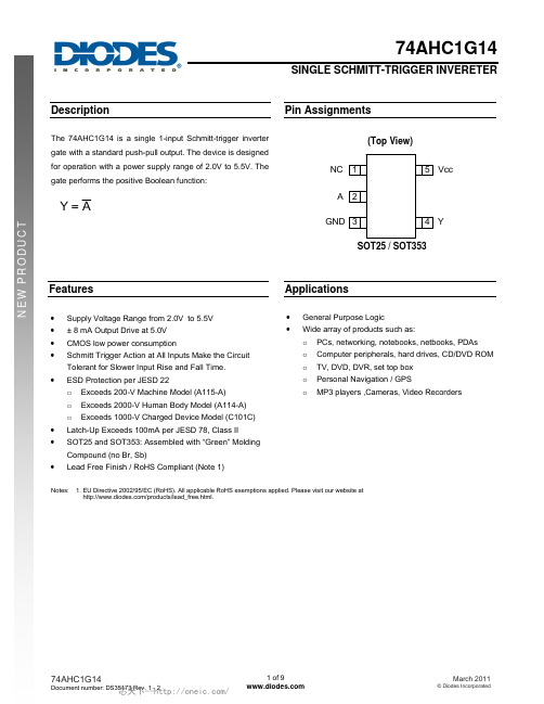
DescriptionThe 74AHC1G14 is a single 1-input Schmitt-trigger inverter gate with a standard push-pull output. The device is designed for operation with a power supply range of 2.0V to 5.5V. The gate performs the positive Boolean function:AY =Pin AssignmentsSOT25 / SOT353NCGND YVcc(Top View)AFeatures• Supply Voltage Range from 2.0V to 5.5V • ± 8 mA Output Drive at 5.0V • CMOS low power consumption• Schmitt Trigger Action at All Inputs Make the Circuit Tolerant for Slower Input Rise and Fall Time. •ESD Protection per JESD 22o Exceeds 200-V Machine Model (A115-A) o Exceeds 2000-V Human Body Model (A114-A) o Exceeds 1000-V Charged Device Model (C101C) • Latch-Up Exceeds 100mA per JESD 78, Class II • SOT25 and SOT353: Assembled with “Green” Molding Compound (no Br, Sb)• Lead Free Finish / RoHS Compliant (Note 1)Applications• General Purpose Logic •Wide array of products such as:o PCs, networking, notebooks, netbooks, PDAs o Computer peripherals, hard drives, CD/DVD ROM o TV, DVD, DVR, set top box o Personal Navigation / GPSo MP3 players ,Cameras, Video RecordersNotes: 1. EU Directive 2002/95/EC (RoHS). All applicable RoHS exemptions applied. Please visit our website at/products/lead_free.html .Pin DescriptionsPin NamePin NO.DescriptionNC 1 NoConnection A 2 Data Input GND 3 Ground Y 4 Data OutputV CC 5 Supply VoltageLogic DiagramFunction TableInputs Output AYH L L HAbsolute Maximum Ratings (Note 2)Symbol Description Rating UnitESD HBM Human Body Model ESD Protection 2 KVESD CDM Charged Device Model ESD Protection 1 KVESD MM Machine Model ESD Protection 200 V V CC Supply Voltage Range -0.5 to 6.5 VV I Input Voltage Range -0.5 to 6.5 VV O Voltage applied to output in high or low state -0.5 to V CC +0.5 VI IK Input Clamp Current V I<0 -20 mAI OK Output Clamp Current (V O < 0 or V O > V CC) ±20 mAI O Continuous output current (V O = 0 to V CC) ±25 mAI CC Continuous current through V CC 50 mAI GND Continuous current through GND -50 mAT J Operating Junction Temperature -40 to 150 °CT STG Storage Temperature -65 to 150 °CNotes: 2. Stresses beyond the absolute maximum may result in immediate failure or reduced reliability. These are stress values and device operation should bewithinrecommendvalues.Recommended Operating Conditions (Note 3)Symbol Parameter Min Max UnitV CC Operating Voltage 2 5.5 V V I Input Voltage 0 5.5 VV O Output Voltage 0 V CC VI OH High-level output current V CC = 2V -50 uA V CC = 3.3V ± 0.3V -4mAV CC = 5V ± 0.5V -8I OL Low-level output current V CC = 2V 50 uA V CC = 5V ± 0.5V 4mAV CC = 3V 8T A Operating free-airtemperature-40 125 ºCNotes: 3. Unused inputs should be held at V CC or Ground.Electrical CharacteristicsSymbol Parameter Test Conditions V CC25ºC -40ºC to 85ºC -40ºC to 125ºCUnit Min Typ. Max Min Max Min MaxV T+Positive-goinginputthresholdvoltage3V 2.2 2.2 2.2 V4.5V 3.15 3.15 3.15 V5.5V 3.85 3.85 3.85 VV T-Negative-goinginputthresholdvoltage3 V 0.9 0.9 0.9 V4.5V 1.35 1.35 1.35 V5.5V 1.65 1.65 1.65 VΔV T Hysteresis(V T+ - V T-)3V 0.3 1.2 0.3 1.2 0.25 1.2 V4.5V 0.4 1.4 0.4 1.4 0.35 1.4 V5.5V 0.5 1.6 0.5 1.6 0.45 1.6V OH High LevelOutput VoltageI OH = -50μA2V 1.9 2 1.9 1.9V3V 2.9 3 2.9 2.94.5V 4.4 4.5 4.4 4.4I OH = -4mA 3V 2.58 2.48 2.40I OH = -8mA 4.5V 3.94 3.8 3.70V OL Low LevelOutput VoltageI OL = 50μA2V 0.1 0.1 0.1V3V 0.1 0.1 0.14.5V 0.1 0.1 0.1I OL = 4mA 3V 0.36 0.44 0.55I OL = 8mA 4.5V 0.36 0.44 0.55I I Input Current V I = 5.5 V or GND 0 to 5.5V± 0.1 ± 1 ± 2 μAI CC Supply Current V I = 5.5V or GNDI O=05.5V 1 10 40 μAC I InputCapacitanceV I = V CC – orGND5.5V 2.0 10 10 10 pFθJA ThermalResistanceJunction-to-AmbientSOT25(Note 4)195o C/W SOT353 430θJC ThermalResistanceJunction-to-CaseSOT25(Note 4)58o C/W SOT353 155Note: 4. Test conditions for SOT25, and SOT353: Device mounted on FR-4 substrate PC board, 2oz copper, with minimum recommended pad layoutSwitching CharacteristicsV CC = 3.3V ± 0.3 (see Figure 1)ParameterFrom (Input) TO (OUTPUT)25ºC -40ºC to 85ºC -40ºC to 125ºCUnitMinTyp.MaxMin Max Min Maxt pdA YC L =15pF0.6 4.2 12.8 0.6 15.0 0.6 16.5 ns C L =50pF0.6 6.0 16.3 0.6 18.5 0.6 20.5 nsV CC = 5V ± 0.5V (see Figure 1)ParameterFrom (Input) TO (OUTPUT)25ºC -40ºC to 85ºC -40ºC to 125ºCUnitMinTyp.MaxMin MaxMin Maxt pdA YC L =15pF0.6 3.2 8.6 0.6 10.0 0.6 11.0 ns C L =50pF0.6 4.6 10.6 0.6 12.0 0.6 13.5 nsOperating CharacteristicsT A = 25 ºCParameterTest Conditions V CC = 5 V Unit Typ. C pdPower dissipation capacitancef = 1 MHz No Load10pFParameter Measurement InformationV CCInputsV M C LVIt r /tf3.3V±0.3VV CC ≤3ns V CC /2 15pF 5V±0.5V V CC ≤3ns V CC /2 15pF 3.3V±0.3V V CC ≤3ns V CC /2 50pF 5V±0.5VV CC≤3nsV CC /250pFVoltage Waveform Pulse DurationVoltage Waveform Propagation Delay TimesInverting and Non Inverting OutputsFigure 1. Load Circuit and Voltage WaveformsNotes: A. Includes test lead and test apparatus capacitance.B. All pulses are supplied at pulse repetition rate ≤ 1 MHz.C. Inputs are measured separately one transition per measurement.D. t PLH and t PHL are the same as t PD .Ordering Information74AHC1G 14XX -7W5:SOT25FunctionPackage7:Tape &ReelPacking 14:1-InputSchmitt-Trigger InverterSE :SOT353Logic Device 74:Logic Prefix AHC :2to Family 1G :One gate5.5VDevice Package Code Packaging (Note 5) 7” Tape and ReelQuantityPart Number Suffix74AHC1G14W5-7 W5 SOT25 3000/Tape & Reel -7 74AHC1G14SE-7SESOT3533000/Tape & Reel-7Notes: 5. Pad layout as shown on Diodes Inc. suggested pad layout document AP02001, which can be found on our website at/datasheets/ap02001.pdf.Marking InformationXX : Identification codeW : Week : A~Z : 1~26 week;X : A~Z : Internal code(Top View)Y : Year 0~9a~z : 27~52 week; z represents 52 and 53 weekPart NumberPackageIdentification Code74AHC1G14W5 SOT25 YV 74AHC1G14SE SOT353YVPackage Outline Dimensions (All Dimensions in mm) (1) Package Type: SOT25(2) Package Type: SOT353SOT25Dim Min Max TypA0.350.500.38B 1.50 1.70 1.60C 2.70 3.00 2.80D ⎯ ⎯ 0.95H 2.90 3.10 3.00J0.0130.100.05K 1.00 1.30 1.10L0.350.550.40M0.100.200.15N0.700.800.75α 0° 8° ⎯All Dimensions in mmSOT353Dim Min MaxA0.10 0.30B 1.15 1.35C 2.00 2.20D0.65 TypF0.40 0.45H 1.80 2.20J0 0.10K0.90 1.00L0.25 0.40M0.10 0.22α 0° 8°All Dimensions in mm。
BP5293_DataSheet_(中文)_VerA_150630
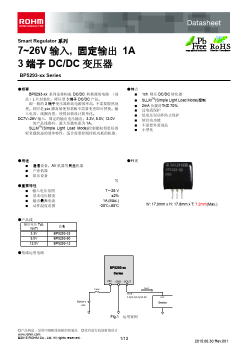
Smart Regulator 系列7~26V 输入, 固定输出 1A 3端子DC/DC 变压器BP5293-xx Series●概要 BP5293-xx 系列是将构成DC/DC 转换器的电路 (部品)1片封装化,降压型3端子DC/DC 产品。
跟一般的3端子变压器相比电源效率高,不需要散热处理。
同时是pin 脚封装使得基板不需要变更即可替换。
输入电容,线圈内置,使得封装设计简单化。
DC7V~26V 输入,固定的输出电压输出。
3.3V, 5.0V, 12.0V 的产品线都有,最大负载电流为1A 。
SLLM TM(Simple Light Load Mode)控制能取得更好的轻负载状态的效率特性,适合需要控制待机功耗的机器。
●特点■ 1ch 降压DC/DC 转化器■ SLLM TM(Simple Light Load Mode)控制 ■ 2mA 负载时効率70% ■ 过电流保护■ 低电压误动作防止保护 ■软启动功能 ■ 不需要外置部品 ■ 小型化●用途■ 通信设备、AV 机器等民生机器 ■ 产业机器 ■娱乐设备等 ●外观W: 17.0mm x H: 17.8mm x T: 7.2mm (Max.)●重要特性■ 输入电压范围 ■ 基本电压精度 ■ 输出最大电流 ■ 动作温度范围7~26 V±2% 1A (Max.) -25℃~85℃●基础运用电路Battery etc.●绝对最大值(Ta=25°C)一定的使用条件、或者一定的实验条件或者瞬间不可超过的值。
●端子配置图123Fig.2端子配置图●内部电路图Fig.3 电路图动作说明1) DC/DC 转换器动作BP5292-xx 是通过电流模式PWM 控制方式来实现高速过渡应答性,降压同步整流开关调整。
重负载状态的Pulse WidthModulation(PWM)模式是在570kHz (typ.)的开光频率下驱动工作,轻负载时为了提高效率进行SSLM TM(Simple Light Load Mode)控制。
安森美三极管详细规格参数表(超全)

Product Datasheet Compliance Status12A02CH ENN7482/D (98.0kB)Pb-free ActiveNEW 15GN01CA15GN01CA/D (48.0kB)Pb-free ActiveNEW 2N2905A2N2905A/D (88.0kB)MIL-PRF-19500ActiveNEW 2N30192N3019/D (85.0kB)MIL-PRF-19500ActiveNEW 2N3019S2N3019S/D (86.0kB)MIL-PRF-19500ActiveNEW 2N37002N3700/D (86.0kB)MIL-PRF-19500ActiveNEW2SA14162SA1416/D (102.0kB)Pb-free ActiveNEW2SA14192SA1419/D (305.0kB)Pb-free ActiveNEW 2SA15932SA1593/D (45.0kB)Pb-free ActiveNEW 2SA17052SA1705/D (40.0kB)Pb-free ActiveNEW 2SA17062SA1706/D (42.0kB)Pb-free ActiveNEW 2SA17072SA1707/D (61.0kB)Pb-free ActiveNEW 2SA17092SA1709/D (49.0kB)Pb-free ActiveNEW 2SA18272SA1827/D (52.0kB)Pb-free ActiveNEW 2SA20122SA2012/D (98.0kB)Pb-free ActiveNEW 2SA20162SA2016/D (57.0kB)Pb-free ActiveNEW 2SA20992SA2099/D (76.0kB)Pb-free ActiveNEW 2SA21122SA2112/D (28.0kB)Pb-free ActiveNEW 2SA21242SA2124/D (91.0kB)Pb-free ActiveNEW2SA21252SA2125/D (59.0kB)Pb-freeHalide free ActiveNEW2SA21262SA2126/D (54.0kB)Pb-free ActiveNEW 2SA21532SA2153/D (35.0kB)Pb-free ActiveNEW 2SA21692SA2169/D (61.0kB)Pb-free ActiveNEW 2SA22022SA2202/D (58.0kB)Pb-free ActiveNEW 2SA22222SA2222/D (69.0kB)Pb-free ActiveNEW 2SB11222SB1122/D (89.0kB)Pb-free ActiveNEW2SB11432SB1143/D (60.0kB)Pb-free ActiveNEW 2SB12012SB1201/D (45.0kB)Pb-free ActiveNEW 2SB12152SB1215/D (60.0kB)Pb-free ActiveNEW 2SB13022SB1302/D (80.0kB)Pb-free ActiveNEW2SC36462SA1416/D (102.0kB)Pb-free ActiveNEW2SC36492SA1419/D (305.0kB)Pb-free ActiveNEW2SC4487ENN3093/D (61.0kB)Pb-free ActiveNEW2SC44882SA1708/D (68.0kB)Pb-free ActiveNEW2SC46142SA1770/D (60.0kB)Pb-free ActiveNEW 2SC47312SC4731/D (52.0kB)Pb-free ActiveNEW 2SC48372SA1855/D (61.0kB)Pb-free ActiveNEW 2SC5226A2SC5226A/D (75.0kB)Pb-free ActiveNEW2SC5227A2SC5227A/D (75.0kB)Pb-free ActiveNEW2SC5231A2SC5231A/D (65.0kB)Pb-free ActiveNEW 2SC5245A2SC5245A/D (58.0kB)Pb-free ActiveNEW 2SC5347A2SC5347A/D (67.0kB)Pb-free ActiveNEW 2SC5415A2SC5415A/D (92.0kB)Pb-free ActiveNEW2SC5488A2SC5488A/D (57.0kB)Pb-freeHalide free ActiveNEW2SC5501A2SC5501A/D (50.0kB)Pb-free ActiveNEW 2SC5551A2SC5551A/D (76.0kB)Pb-free ActiveNEW2SC57062SA2039/D (61.0kB)Pb-freeHalide free ActiveNEW2SC59942SC5994/D (36.0kB)Pb-free ActiveNEW 2SC60172SA2169/D (61.0kB)Pb-free ActiveNEW 2SC60432SC6043/D (30.0kB)Pb-free ActiveNEW 2SC60962SC6096/D (47.0kB)Pb-free ActiveNEW 2SC60972SC6097/D (51.0kB)Pb-free ActiveNEW 2SC61442SC6144/D (68.0kB)Pb-free ActiveNEW2SD12072SB892/D (62.0kB)Pb-free ActiveNEW 2SD16202SD1620/D (85.0kB)Pb-free ActiveNEW2SD16232SB1123/D (99.0kB)Pb-free ActiveNEW 2SD18012SD1801/D (45.0kB)Pb-free ActiveNEW 2SD18052SD1805/D (96.0kB)Pb-free ActiveNEW 2SD18152SB1215/D (60.0kB)Pb-free ActiveNEW 2SD18162SB1216/D (60.0kB)Pb-free ActiveNEW2SD18352SB1229/D (61.0kB)Pb-free ActiveNEW 30A02CH30A02CH/D (28.0kB)Pb-free ActiveNEW 30A02MH30A02MH/D (28.0kB)Pb-free ActiveNEW 30C02CH30C02CH/D (28.0kB)Pb-free ActiveNEW 50A02MH50A02MH/D (29.0kB)Pb-free ActiveNEW 55GN01CA55GN01CA/D (50.0kB)Pb-free ActiveNEWBC807-25W BC807-25W/D (105.0kB)AEC QualifiedPPAP CapablePb-freeHalide free ActiveNEWBC807-40W BC807-25W/D (105.0kB)AEC QualifiedPPAP CapablePb-freeHalide free ActiveNEWBCW66BCW66GLT1/D (110.0kB)Pb-freeHalide freeAEC QualifiedPPAP Capable ActiveNEWCPH3105CPH3105/D (39.0kB)Pb-free ActiveNEW CPH3106CPH3106/D (33.0kB)Pb-free ActiveNEW CPH3109CPH3109/D (55.0kB)Pb-free ActiveNEW CPH3115CPH3115/D (54.0kB)Pb-free ActiveNEW CPH3116CPH3116/D (46.0kB)Pb-free ActiveNEWCPH3121CPH3121/D (65.0kB)Pb-free ActiveNEW CPH3122CPH3122/D (58.0kB)Pb-free ActiveNEW CPH3123CPH3123/D (43.0kB)Pb-free ActiveNEW CPH3140CPH3140/D (37.0kB)Pb-free ActiveNEW CPH3145CPH3145/D (44.0kB)Pb-free ActiveNEW CPH3205CPH3205/D (39.0kB)Pb-free ActiveNEW CPH3209CPH3209/D (55.0kB)Pb-free ActiveNEW CPH3215CPH3215/D (54.0kB)Pb-free ActiveNEW CPH3216CPH3216/D (46.0kB)Pb-free ActiveNEW CPH3223CPH3223/D (43.0kB)Pb-free ActiveNEW CPH3240CPH3240/D (37.0kB)Pb-free ActiveNEW CPH3245CPH3245/D (44.0kB)Pb-free ActiveNEW CPH5504CPH5504/D (49.0kB)Pb-free ActiveNEW CPH5506CPH5506/D (74.0kB)Pb-free ActiveNEW CPH5517CPH5517/D (45.0kB)Pb-free ActiveNEW CPH5524CPH5524/D (72.0kB)Pb-free ActiveNEW CPH6001A CPH6001A/D (63.0kB)Pb-free ActiveNEW CPH6003A CPH6003A/D (58.0kB)Pb-free ActiveNEW CPH6020CPH6020/D (258.0kB)Pb-free ActiveNEWCPH6021ENA1910/D (372.0kB)Pb-freeHalide free ActiveNEWCPH6121CPH6121/D (47.0kB)Pb-free ActiveNEW CPH6122CPH6122/D (48.0kB)Pb-free ActiveNEW CPH6123CPH6123/D (55.0kB)Pb-free ActiveNEW CPH6153CPH6153/D (255.0kB)Pb-free ActiveNEW CPH6223CPH6123/D (55.0kB)Pb-free ActiveNEW CPH6501CPH6501/D (65.0kB)Pb-free ActiveNEWEC3H02BA EC3H02BA/D (283.0kB)Pb-freeHalide free ActiveNEWEC4H09C EC4H09C/D (52.0kB)Pb-freeHalide free ActiveNEWECH8501ECH8501/D (421.0kB)Pb-freeHalide free ActiveNEWMCH3007MCH3007/D (326.0kB)Pb-freeHalide free ActiveNEWMCH4014MCH4014/D (355.0kB)Pb-freeHalide free ActiveNEWMCH4015MCH4015/D (354.0kB)Pb-freeHalide free ActiveNEWMCH4016MCH4016/D (355.0kB)Pb-freeHalide free ActiveNEWMCH4017MCH4017/D (355.0kB)Pb-freeHalide free ActiveNEWMCH4020MCH4020/D (283.0kB)Pb-free ActiveNEW MCH4021MCH4021/D (283.0kB)Pb-free ActiveNEW MCH5541MCH5541/D (48.0kB)Pb-free ActiveNEW MCH6102MCH6102/D (39.0kB)Pb-free ActiveNEW MCH6202MCH6202/D (39.0kB)Pb-free ActiveNEW MCH6541MCH6541/D (65.0kB)Pb-free ActiveNEW MCH6542MCH6542/D (60.0kB)Pb-free ActiveNEW MCH6544MCH6544/D (57.0kB)Pb-free ActiveNEWMCH6545MCH6545/D (52.0kB)Pb-free ActiveNEWMSD1819A-R MSD1819A-RT1/D (209.0kB Pb-free Halide free AEC QualifiedPPAP CapableActiveNEW NSM6056MT1G NSM6056M/D (102.0kB)Pb-freeHalide freeActiveNEW NSM80100M NSM80100M/D (109.0kB)Pb-freeHalide freeActiveNEW NSM80101M NSM80101M/D (108.0kB)Pb-freeHalide freeActiveNEW PCP1103PCP1103/D (266.0kB)Pb-freeHalide freeActiveNEW PCP1203PCP1203/D (267.0kB)Pb-freeHalide free ActiveNEW15C02CH 15C02CH/D (44.0kB)Pb-free Active 2N2907A 2N2907A/D (89.0kB)MIL-PRF-19500Active 2N30552N3055/D (70.0kB)Pb-free Active 2N3055A 2N3055A/D (89.0kB)Pb-free Active 2N34422N3442/D (65.0kB)Pb-free Active 2N37712N3771/D (85.0kB)Pb-free Active 2N37722N3771/D (85.0kB)Pb-free Active 2N37732N3773/D (93.0kB)Pb-free Active 2N39042N3903/D (177.0kB)Pb-free Active 2N39062N3906/D (173.0kB)Pb-free Active 2N41242N4123/D (115.0kB)Pb-free Active 2N44012N4401/D (195.0kB)Pb-free Active 2N44032N4403/D (118.0kB)Pb-freeActive 2N49182N4918/D (117.0kB)Pb-freeHalide freeActive 2N49192N4918/D (117.0kB)Pb-freeHalide freeActive 2N49202N4918/D (117.0kB)Pb-freeHalide freeActive 2N49212N4921/D (90.0kB)Pb-freeHalide freeActive 2N49222N4921/D (90.0kB)Pb-freeHalide freeActive 2N49232N4921/D (90.0kB)Pb-freeHalide free Active 2N50382N5038/D (79.0kB)Pb-free Active 2N50872N5087/D (155.0kB)Pb-free Active 2N50882N5088/D (83.0kB)Pb-free Active 2N50892N5088/D (83.0kB)Pb-freeActive 2N51902N5191/D (84.0kB)Pb-freeHalide freeActive 2N51912N5191/D (84.0kB)Pb-freeHalide freeActive 2N51922N5191/D (84.0kB)Pb-freeHalide freeActive2N51942N5194/D (86.0kB)Pb-freeHalide free Active2N51952N5194/D (86.0kB)Pb-freeHalide free Active2N53022N5302/D (92.0kB)Pb-free Active 2N54012N5401/D (145.0kB)Pb-free Active 2N55502N5550/D (88.0kB)Pb-free Active 2N55512N5550/D (88.0kB)Pb-free Active2N56552N5655/D (80.0kB)Pb-freeHalide free Active2N56572N5655/D (80.0kB)Pb-freeHalide free Active2N56842N5684/D (114.0kB)Pb-free Active 2N56862N5684/D (114.0kB)Pb-free Active 2N58832N5883/D (94.0kB)Pb-free Active 2N58842N5883/D (94.0kB)Pb-free Active 2N58852N5883/D (94.0kB)Pb-free Active 2N58862N5883/D (94.0kB)Pb-free Active 2N61072N6107/D (90.0kB)Pb-free Active 2N61092N6107/D (90.0kB)Pb-free Active 2N61112N6107/D (90.0kB)Pb-free Active 2N62882N6107/D (90.0kB)Pb-free Active 2N62922N6107/D (90.0kB)Pb-free Active 2N63382N6338/D (135.0kB)Pb-free Active 2N63412N6338/D (135.0kB)Pb-free Active 2N64872N6487/D (92.0kB)Pb-free Active 2N64882N6487/D (92.0kB)Pb-free Active 2N64902N6487/D (92.0kB)Pb-free Active 2N64912N6487/D (92.0kB)Pb-free Active 2N65202N6515/D (116.0kB)Pb-free Active 2SA10202SA1020/D (93.0kB)Pb-free Active 2SA14172SA1417/D (57.0kB)Pb-free Active 2SA17082SA1708/D (68.0kB)Pb-free Active 2SA17702SA1770/D (60.0kB)Pb-free Active2SA17742SA1774/D (53.0kB)Pb-freeHalide free Active2SA20132SA2013/D (57.0kB)Pb-free Active2SA2029M32SA2029M3/D (45.0kB)Pb-freeHalide free Active2SA20392SA2039/D (61.0kB)Pb-free Active 2SB11232SB1123/D (99.0kB)Pb-free Active 2SB11242SB1124/D (44.0kB)Pb-free Active2SB12022SB1202/D (58.0kB)Pb-free Active 2SB12042SB1204/D (103.0kB)Pb-free Active2SB12052SB1205/D (50.0kB)Pb-free Active2SC33322SA1319/D (59.0kB)Pb-free Active2SC36472SA1417/D (57.0kB)Pb-free Active 2SC36482SA1418/D (96.0kB)Pb-free Active2SC46172SC4617/D (45.0kB)Pb-freeHalide free Active2SC55662SA2013/D (57.0kB)Pb-free Active 2SC55692SA2016/D (57.0kB)Pb-free Active2SC5658M3T5G2SC5658M3/D (125.0kB)Pb-freeHalide free Active2SC5658RM3T5G2SC5658M3/D (125.0kB)Pb-freeHalide free Active2SC57072SA2040/D (58.0kB)Pb-free Active 2SC58882SA2099/D (76.0kB)Pb-free Active 2SC59642SA2125/D (59.0kB)Pb-free Active 2SC60822SC6082/D (52.0kB)Pb-free Active 2SC60942SC6094/D (49.0kB)Pb-free Active 2SC60952SC6095/D (49.0kB)Pb-free Active 2SD16242SD1624/D (44.0kB)Pb-free Active 2SD16852SD1685/D (113.0kB)Pb-free Active 2SD18022SB1202/D (58.0kB)Pb-free Active BC237B BC237/D (59.0kB)Pb-free Active BC307B BC307/D (87.0kB)Pb-free Active BC327BC327/D (102.0kB)Pb-free Active BC327-025BC327/D (102.0kB)Pb-free Active BC327-25BC327/D (102.0kB)Pb-free Active BC337BC337/D (141.0kB)Pb-free Active BC337-025BC337/D (141.0kB)Pb-free Active BC337-040BC337/D (141.0kB)Pb-free Active BC337-25BC337/D (141.0kB)Pb-free Active BC337-40BC337/D (141.0kB)Pb-free Active BC369BC368/D (60.0kB)Pb-free Active BC490BC490/D (78.0kB)Pb-free Active BC546B BC546/D (72.0kB)Pb-free Active BC547B BC546/D (72.0kB)Pb-free Active BC547C BC546/D (72.0kB)Pb-free Active BC548B BC546/D (72.0kB)Pb-free Active BC548C BC546/D (72.0kB)Pb-free Active BC549C BC549B/D (53.0kB)Pb-free Active BC550C BC550C/D (59.0kB)Pb-free Active BC556B BC556B/D (81.0kB)Pb-free Active BC557B BC556B/D (81.0kB)Pb-free Active BC557C BC556B/D (81.0kB)Pb-free Active BC558B BC556B/D (81.0kB)Pb-free Active BC560C BC560C/D (131.0kB)Pb-free Active BC637BC635/D (92.0kB)Pb-free Active BC639BC635/D (92.0kB)Pb-free Active BC640BC640/D (88.0kB)Pb-free ActiveBC807-16L BC807-16LT1/D (118.0kB)Pb-freeHalide freeActive BC807-25L BC807-16LT1/D (118.0kB)Pb-freeHalide freeActive BC807-40L BC807-16LT1/D (118.0kB)Pb-freeHalide freeActive BC808BC808-25LT1/D (128.0kB)Pb-freeHalide freeActive BC817-16L BC817-16LT1/D (119.0kB)Pb-freeHalide freeActive BC817-25L BC817-16LT1/D (119.0kB)Pb-freeHalide freeActive BC817-40L BC817-16LT1/D (119.0kB)Pb-freeHalide freeActive BC818BC818-40LT/D (128.0kB)Pb-freeHalide freeActive BC846AL BC846ALT1/D (131.0kB)Pb-freeHalide freeActive BC846B BC846BDW1T1/D (127.0kB Pb-freeHalide freeActive BC846BL BC846ALT1/D (131.0kB)Pb-freeHalide freeActive BC846BM3T5G BC846BM3/D (87.0kB)Pb-freeHalide freeActive BC846BPDW1BC846BPDW1T1/D (166.0k Pb-freeHalide freeActive BC846BW BC846AWT1/D (128.0kB)Pb-freeHalide freeActive BC846C BC846BDW1T1/D (127.0kB Pb-freeHalide freeActive BC847AL BC846ALT1/D (131.0kB)Pb-freeHalide freeActive BC847AW BC846AWT1/D (128.0kB)Pb-freeHalide freeActive BC847BDW1BC846BDW1T1/D (127.0kB Pb-freeHalide freeActive BC847BL BC846ALT1/D (131.0kB)Pb-freeHalide freeActive BC847BP BC846BPDW1T1/D (166.0k Pb-freeHalide freeActive BC847BPDXV6BC847BPDXV6T1/D (76.0kB Pb-freeHalide freeActive BC847BT BC847ATT1/D (71.0kB)Pb-freeHalide freeActive BC847BW BC846AWT1/D (128.0kB)Pb-freeHalide freeActive BC847CDXV6BC847CDXV6T1/D (96.0kB)Pb-freeHalide freeActiveBC847CL BC846ALT1/D (131.0kB)AEC Qualified PPAP Capable Pb-freeHalide freeActive BC847CT BC847ATT1/D (71.0kB)Pb-freeHalide freeActive BC847CW BC846AWT1/D (128.0kB)Pb-freeHalide freeActive BC848AL BC846ALT1/D (131.0kB)Pb-freeHalide freeActive BC848BL BC846ALT1/D (131.0kB)Pb-freeHalide freeActive BC848BW BC846AWT1/D (128.0kB)Pb-freeHalide freeActive BC848CDW1BC846BDW1T1/D (127.0kB Pb-freeHalide freeActive BC848CL BC846ALT1/D (131.0kB)Pb-freeHalide freeActive BC848CPD BC846BPDW1T1/D (166.0k Pb-freeHalide freeActive BC848CW BC846AWT1/D (128.0kB)Pb-freeHalide freeActive BC849BL BC846ALT1/D (131.0kB)Pb-freeHalide freeActive BC849CL BC846ALT1/D (131.0kB)Pb-freeHalide freeActive BC850BL BC846ALT1/D (131.0kB)Pb-freeHalide freeActive BC850CL BC846ALT1/D (131.0kB)Pb-freeHalide freeActive BC856 SERIES BC856BM3/D (55.0kB)Pb-freeHalide freeActive BC856AL BC856ALT1/D (167.0kB)Pb-freeHalide freeActive BC856B BC856BDW1T1/D (172.0kB Pb-freeHalide freeActive BC856BL BC856ALT1/D (167.0kB)Pb-freeHalide freeActive BC856BW BC856BWT1/D (143.0kB)Pb-freeHalide freeActive BC857AL BC856ALT1/D (167.0kB)Pb-freeHalide freeActive BC857BDW1BC856BDW1T1/D (172.0kB Pb-freeHalide freeActive BC857BL BC856ALT1/D (167.0kB)Pb-freeHalide freeActive BC857BT BC857BTT1/D (74.0kB)Pb-freeHalide freeActive BC857BWBC856BWT1/D (143.0kB)Pb-freeHalide freeActiveBC857CDW1BC856BDW1T1/D (172.0kB Pb-freeHalide freeActive BC857CL BC856ALT1/D (167.0kB)Pb-freeHalide freeActive BC857CW BC856BWT1/D (143.0kB)Pb-freeHalide freeActive BC858AL BC856ALT1/D (167.0kB)Pb-freeHalide freeActive BC858AW BC856BWT1/D (143.0kB)Pb-freeHalide freeActive BC858BL BC856ALT1/D (167.0kB)Pb-freeHalide freeActive BC858BW BC856BWT1/D (143.0kB)Pb-freeHalide freeActive BC858CDXV6BC858CDXV6T1/D (56.0kB)Pb-freeHalide freeActive BC858CLBC856ALT1/D (167.0kB)Pb-freeHalide freeActiveBCP53BCP53T1/D (101.0kB)Pb-free Halide freeActiveBCP56BCP56T1/D (104.0kB)Pb-freeHalide freeActive BCP68BCP68T1/D (128.0kB)Pb-freeHalide freeActive BCP69BCP69T1/D (96.0kB)Pb-freeHalide freeActive BCW30L BCW30LT1/D (240.0kB)Pb-freeHalide freeActive BCW32L BCW32LT1/D (192.0kB)Pb-freeHalide freeActive BCW33L BCW33LT1/D (257.0kB)Pb-freeHalide freeActive BCW65AL BCW65ALT1/D (110.0kB)Pb-freeHalide freeActive BCW68GL BCW68GLT1/D (108.0kB)Pb-freeHalide freeActive BCW70L BCW70LT1/D (265.0kB)Pb-freeHalide freeActive BCW72L BCW72LT1/D (277.0kB)Pb-freeHalide freeActive BCX17L BCX17LT1/D (92.0kB)Pb-freeHalide freeActive BCX19L BCX17LT1/D (92.0kB)Pb-freeHalide freeActive BD135BD135/D (37.0kB)Pb-freeHalide freeActive BD136BD136/D (37.0kB)Pb-freeHalide freeActiveBD137BD135/D (37.0kB)Pb-freeHalide free ActiveBD138BD136/D (37.0kB)Pb-freeHalide free ActiveBD139BD135/D (37.0kB)Pb-freeHalide free ActiveBD140BD136/D (37.0kB)Pb-freeHalide free ActiveBD159BD159/D (56.0kB)Pb-freeHalide free ActiveBD179BD179/D (80.0kB)Pb-freeHalide free ActiveBD180BD180/D (62.0kB)Pb-freeHalide free ActiveBD234BD237/D (63.0kB)Pb-freeHalide free ActiveBD237BD237/D (63.0kB)Pb-freeHalide free ActiveBD241C BD241C/D (93.0kB)Pb-free Active BD242B BD241C/D (93.0kB)Pb-free Active BD242C BD241C/D (93.0kB)Pb-free Active BD243C BD243B/D (91.0kB)Pb-free Active BD244B BD243B/D (91.0kB)Pb-free Active BD244C BD243B/D (91.0kB)Pb-free ActiveBD435BD437/D (59.0kB)Pb-freeHalide free ActiveBD436BD438/D (58.0kB)Pb-freeHalide free ActiveBD437BD437/D (59.0kB)Pb-freeHalide free ActiveBD438BD438/D (58.0kB)Pb-freeHalide free ActiveBD439BD437/D (59.0kB)Pb-freeHalide free ActiveBD440BD438/D (58.0kB)Pb-freeHalide free ActiveBD441BD437/D (59.0kB)Pb-freeHalide free ActiveBD442BD438/D (58.0kB)Pb-freeHalide free ActiveBD787BD787/D (78.0kB)Pb-freeHalide free ActiveBD788BD787/D (78.0kB)Pb-freeHalide free ActiveBD809BD809/D (80.0kB)Pb-free Active BD810BD809/D (80.0kB)Pb-free Active BF422BF422/D (98.0kB)Pb-free Active BF423BF421/D (105.0kB)Pb-free Active BF493S BF493S/D (58.0kB)Pb-free ActiveBF720BF720T1/D (128.0kB)Pb-freeHalide free ActiveBF721BF721T1/D (127.0kB)Pb-freeHalide freeActive BSP16BSP16T1/D (112.0kB)Pb-freeHalide freeActive BSP19A BSP19AT1/D (181.0kB)Pb-freeHalide freeActive BSS63L BSS63LT1/D (111.0kB)Pb-freeHalide freeActive BSS64L BSS64LT1/D (108.0kB)Pb-freeHalide freeActive BSV52L BSV52LT1/D (108.0kB)Pb-freeHalide free ActiveBU406BU406/D (121.0kB)Pb-freeActive BUD42D BUD42D/D (178.0kB)Pb-freeHalide free Active BUH100BUH100/D (246.0kB)Pb-free Active BUH150BUH150/D (238.0kB)Pb-free Active BUH50BUH50/D (247.0kB)Pb-free Active BUL45BUL45/D (205.0kB)Pb-free Active BUL45D2BUL45D2/D (231.0kB)Pb-free Active BUV21BUV21/D (70.0kB)Pb-free Active BUV22BUV22/D (70.0kB)Pb-free Active BUV26BUV26/D (85.0kB)Pb-free Active BUV27BUV27/D (52.0kB)Pb-free Active BUX85BUX85/D (128.0kB)Pb-free Active CPH6531CPH6531/D (59.0kB)Pb-free Active CPH6532CPH6532/D (48.0kB)Pb-free Active D44H11D44H/D (81.0kB)Pb-free Active D44H8D44H/D (81.0kB)Pb-free Active D44VH D44VH/D (84.0kB)Pb-free Active D45C D45C12/D (73.0kB)Pb-free Active D45H11D44H/D (81.0kB)Pb-free Active D45H8D44H/D (81.0kB)Pb-free Active D45VH D44VH/D (84.0kB)Pb-freeActive EMT SERIES EMT1DXV6T1/D (51.0kB)Pb-freeHalide freeActive EMX1EMX1DXV6T1/D (51.0kB)Pb-freeHalide freeActive EMX2DXV6EMX2DXV6T5/D (121.0kB)Pb-freeHalide freeActive EMZ1EMZ1DXV6/D (59.0kB)Pb-freeHalide free Active FH102A FH102A/D (64.0kB)Pb-freeActive HN1B01FDW1HN1B01FDW1T1/D (52.0kB Pb-freeHalide freeActive MBT2222ADW1T1MBT2222ADW1T1/D (164.0Pb-freeHalide freeActive MBT3904DW1MBT3904DW1T1/D (131.0kB Pb-freeHalide freeActive MBT3906DW1MBT3906DW1T1/D (178.0kB Pb-freeHalide freeActiveMBT3946DW1T1MBT3946DW1T1/D (241.0kB Pb-freeHalide freeActive MBT6429DW1MBT6429DW1T1/D (219.0kB Pb-freeHalide freeActive MCH4009MCH4009/D (66.0kB)Pb-freeHalide free ActiveMCH6001MCH6001/D (251.0kB)Pb-free Active MJ14002MJ14001/D (90.0kB)Pb-free Active MJ29552N3055/D (70.0kB)Pb-free Active MJ4502MJ4502/D (128.0kB)Pb-free Active MJ802MJ802/D (70.0kB)Pb-freeActive MJB41C MJB41C/D (84.0kB)Pb-freeHalide freeActive MJB42C MJB41C/D (84.0kB)Pb-freeHalide freeActive MJB44H11MJB44H11/D (64.0kB)Pb-freeHalide freeActive MJB45H11MJB44H11/D (64.0kB)Pb-freeHalide freeActive MJD148MJD148/D (109.0kB)Pb-freeHalide freeActive MJD200MJD200/D (132.0kB)Pb-freeHalide freeActive MJD210MJD200/D (132.0kB)Pb-freeHalide freeActive MJD243MJD243/D (143.0kB)Pb-freeHalide freeActive MJD253MJD243/D (143.0kB)Pb-freeHalide freeActive MJD2955MJD2955/D (117.0kB)Pb-freeHalide freeActive MJD3055MJD2955/D (117.0kB)Pb-freeHalide freeActive MJD31MJD31/D (129.0kB)Pb-freeHalide freeActive MJD31C MJD31/D (129.0kB)Pb-freeHalide freeActive MJD32MJD31/D (129.0kB)Pb-freeHalide freeActive MJD32C MJD31/D (129.0kB)Pb-freeHalide freeActive MJD340MJD340/D (120.0kB)Pb-freeHalide freeActive MJD350MJD340/D (120.0kB)Pb-freeHalide freeActive MJD41C MJD41C/D (117.0kB)Pb-freeHalide freeActive MJD42C MJD41C/D (117.0kB)Pb-freeHalide freeActive MJD44E3MJD44E3/D (89.0kB)Pb-freeHalide freeActiveMJD44H11MJD44H11/D (108.0kB)Pb-freeHalide free ActiveMJD45H11MJD44H11/D (108.0kB)Pb-freeHalide free ActiveMJD47MJD47/D (110.0kB)Pb-freeHalide free ActiveMJD50MJD47/D (110.0kB)Pb-freeHalide free ActiveMJD5731MJD5731/D (114.0kB)Pb-freeHalide free ActiveMJE13003MJE13003/D (107.0kB)Pb-freeHalide free ActiveMJE13005MJE13005/D (150.0kB)Pb-free Active MJE13007MJE13007/D (194.0kB)Pb-free Active MJE13009MJE13009/D (189.0kB)Pb-free Active MJE15033MJE15032/D (75.0kB)Pb-free ActiveMJE171MJE171/D (82.0kB)Pb-freeHalide free ActiveMJE172MJE171/D (82.0kB)Pb-freeHalide free ActiveMJE18004MJE18004/D (225.0kB)Pb-free Active MJE18008MJE18008/D (229.0kB)Pb-free ActiveMJE181MJE171/D (82.0kB)Pb-freeHalide free ActiveMJE182MJE171/D (82.0kB)Pb-freeHalide free ActiveMJE200MJE200/D (115.0kB)Pb-freeHalide free ActiveMJE210MJE200/D (115.0kB)Pb-freeHalide free ActiveMJE243MJE243/D (187.0kB)Pb-freeHalide free ActiveMJE253MJE243/D (187.0kB)Pb-freeHalide free ActiveMJE2955T MJE2955T/D (138.0kB)Pb-free Active MJE3055T MJE2955T/D (138.0kB)Pb-free ActiveMJE340MJE340/D (67.0kB)Pb-freeHalide free ActiveMJE3439MJE3439/D (54.0kB)Pb-freeHalide free ActiveMJE344MJE344/D (62.0kB)Pb-freeHalide free ActiveMJE350MJE350/D (133.0kB)Pb-freeHalide free ActiveMJE371MJE371/D (61.0kB)Pb-freeHalide free ActiveMJE4343MJE4343/D (142.0kB)Pb-free Active MJE5730MJE5730/D (76.0kB)Pb-free Active MJE5731MJE5730/D (76.0kB)Pb-free Active MJE5731A MJE5730/D (76.0kB)Pb-free Active MJE5850MJE5850/D (104.0kB)Pb-free ActiveMJE5851MJE5850/D (104.0kB)Pb-free Active MJE5852MJE5850/D (104.0kB)Pb-free Active MJF15030MJF15030/D (134.0kB)Pb-free Active MJF15031MJF15030/D (134.0kB)Pb-free Active MJF18004MJE18004/D (225.0kB)Pb-free Active MJF18008MJE18008/D (229.0kB)Pb-free Active MJF2955MJF3055/D (115.0kB)Pb-free Active MJF3055MJF3055/D (115.0kB)Pb-free Active MJF31C MJF31C/D (122.0kB)Pb-free Active MJF32C MJF31C/D (122.0kB)Pb-free Active MJF44H11MJF44H11/D (151.0kB)Pb-free Active MJF45H11MJF44H11/D (151.0kB)Pb-free Active MJF47MJF47/D (130.0kB)Pb-free Active MJW18020MJW18020/D (131.0kB)Pb-free Active MMBT2131MMBT2131T1/D (60.0kB)Pb-freeHalide freeActive MMBT2222AL MMBT2222LT1/D (126.0kB)Pb-freeHalide freeActive MMBT2222AM3MMBT2222AM3/D (168.0kB Pb-freeHalide freeActive MMBT2222AT MMBT2222ATT1/D (114.0kB Pb-freeHalide freeActive MMBT2222AW MMBT2222AWT1/D (121.0k Pb-freeHalide freeActive MMBT2222L MMBT2222LT1/D (126.0kB)Pb-freeHalide freeActive MMBT2369AL MMBT2369LT1/D (190.0kB)Pb-freeHalide freeActive MMBT2369L MMBT2369LT1/D (190.0kB)Pb-freeHalide freeActive MMBT2484L MMBT2484LT1/D (191.0kB)Pb-freeHalide freeActive MMBT2907AL MMBT2907ALT1/D (114.0kB Pb-freeHalide freeActive MMBT2907AM3T5G MMBT2907AM3/D (167.0kB Pb-freeHalide freeActive MMBT2907AW MMBT2907AWT1/D (83.0kB Pb-freeHalide freeActive MMBT3416L MMBT3416LT3/D (230.0kB)Pb-freeHalide freeActive MMBT3904L MMBT3904LT1/D (114.0kB)Pb-freeHalide freeActiveMMBT3904T MMBT3904TT1/D (102.0kB)Pb-free Halide free AEC QualifiedPPAP CapableActive MMBT3904W MMBT3904WT1/D (160.0kB Pb-freeHalide freeActive MMBT3906L MMBT3906LT1/D (120.0kB)Pb-freeHalide freeActiveMMBT3906T MMBT3906TT1/D (86.0kB)Pb-freeHalide freeActive MMBT3906W MMBT3904WT1/D (160.0kB Pb-freeHalide freeActive MMBT4124MMBT4124LT1/D (144.0kB)Pb-freeHalide freeActive MMBT4126LT1MMBT4126LT1/D (154.0kB)Pb-freeHalide freeActive MMBT4401L MMBT4401LT1/D (155.0kB)Pb-freeHalide freeActive MMBT4401M3T5G MMBT4401M3/D (125.0kB)Pb-freeHalide freeActive MMBT4401WT1MMBT4401WT1/D (180.0kB Pb-freeHalide freeActive MMBT4403L MMBT4403LT1/D (151.0kB)Pb-freeHalide freeActive MMBT4403M3T5G MMBT4403M3/D (125.0kB)Pb-freeHalide freeActive MMBT4403W MMBT4403WT1/D (178.0kB Pb-freeHalide freeActive MMBT489MMBT489LT1/D (121.0kB)Pb-freeHalide freeActive MMBT5087L MMBT5087LT1/D (231.0kB)Pb-freeHalide freeActive MMBT5088L MMBT5088LT1/D (192.0kB)Pb-freeHalide freeActive MMBT5089L MMBT5088LT1/D (192.0kB)Pb-freeHalide freeActive MMBT5401L MMBT5401LT1/D (115.0kB)Pb-freeHalide freeActive MMBT5550L MMBT5550LT1/D (121.0kB)Pb-freeHalide freeActive MMBT5551L MMBT5550LT1/D (121.0kB)Pb-freeHalide freeActive MMBT5551M3T5G MMBT5551M3/D (151.0kB)Pb-freeHalide freeActive MMBT6428L MMBT6428LT1/D (194.0kB)Pb-freeHalide freeActive MMBT6429L MMBT6428LT1/D (194.0kB)Pb-freeHalide freeActive MMBT6517L MMBT6517LT1/D (176.0kB)Pb-freeHalide freeActive MMBT6520L MMBT6520LT1/D (116.0kB)Pb-freeHalide freeActive MMBT6521L MMBT6521LT1/D (289.0kB)Pb-freeHalide freeActive MMBT8099L MMBT8099LT1/D (158.0kB)Pb-freeHalide freeActive MMBT918LMMBT918LT1/D (113.0kB)Pb-freeHalide freeActiveMMBTA05L MMBTA05LT1/D (103.0kB)Pb-freeHalide freeActive MMBTA06L MMBTA05LT1/D (103.0kB)Pb-freeHalide freeActive MMBTA06WT1MMBTA06WT1/D (133.0kB)Pb-freeHalide freeActive MMBTA42L MMBTA42LT1/D (89.0kB)Pb-freeHalide freeActive MMBTA55L MMBTA55LT1/D (103.0kB)Pb-freeHalide freeActive MMBTA56L MMBTA55LT1/D (103.0kB)Pb-freeHalide freeActive MMBTA56W MMBTA56WT1/D (132.0kB)Pb-freeHalide freeActive MMBTA70L MMBTA70LT1/D (240.0kB)Pb-freeHalide freeActive MMBTA92L MMBTA92LT1/D (105.0kB)Pb-freeHalide freeActive MMBTH10L MMBTH10LT1/D (123.0kB)Pb-freeHalide freeActive MMBTH10M3T5G MMBTH10M3/D (119.0kB)Pb-freeHalide freeActive MMJT350T1MMJT350T1/D (102.0kB)Pb-freeHalide free ActiveMPS2222MPS2222/D (90.0kB)Pb-free Active MPS2222A MPS2222/D (90.0kB)Pb-free Active MPS2907A MPS2907A/D (129.0kB)Pb-free Active MPS4124MPS4124/D (48.0kB)Pb-free Active MPS4250MPS4250/D (86.0kB)Pb-free Active MPS5172MPS5172/D (98.0kB)Pb-free Active MPS650MPS650/D (68.0kB)Pb-free Active MPS651MPS650/D (68.0kB)Pb-free Active MPS6652MPS6601/D (86.0kB)Pb-free Active MPS6726MPS6726/D (93.0kB)Pb-free Active MPS750MPS650/D (68.0kB)Pb-free Active MPS751MPS650/D (68.0kB)Pb-free Active MPS8099MPS8099/D (122.0kB)Pb-free Active MPSA05MPSA05/D (89.0kB)Pb-free Active MPSA06MPSA05/D (89.0kB)Pb-free Active MPSA18MPSA18/D (79.0kB)Pb-free Active MPSA42MPSA42/D (102.0kB)Pb-free Active MPSA44MPSA44/D (66.0kB)Pb-free Active MPSA55MPSA05/D (89.0kB)Pb-free Active MPSA56MPSA05/D (89.0kB)Pb-free Active MPSA92MPSA92/D (104.0kB)Pb-free Active MPSH10MPSH10/D (82.0kB)Pb-free Active MPSW01MPSW01/D (95.0kB)Pb-free Active MPSW01A MPSW01/D (95.0kB)Pb-free Active MPSW05MPSW05/D (96.0kB)Pb-free Active MPSW06MPSW05/D (96.0kB)Pb-free Active MPSW42MPSW42/D (96.0kB)Pb-freeActiveMPSW51MPSW51/D (96.0kB)Pb-free ActiveMPSW55MPSW55/D (97.0kB)Pb-free Active MPSW56MPSW55/D (97.0kB)Pb-free Active MPSW92MPSW92/D (98.0kB)Pb-free Active MSA1162MSA1162GT1/D (41.0kB)Pb-freeHalide freeActive MSB1218A-RT1MSB1218A-RT1/D (117.0kB Pb-freeHalide freeActive MSB709-RT1MSB709-RT1/D (42.0kB)Pb-freeHalide freeActive MSB92MSB92T1G/D (73.0kB)Pb-freeHalide freeActive MSB92A MSB92ASWT1/D (85.0kB)Pb-freeHalide freeActive MSB92AW MSB92WT1/D (117.0kB)Pb-freeHalide freeActive MSB92W MSB92WT1/D (117.0kB)Pb-freeHalide freeActive MSC2712GT1MSC2712GT1/D (31.0kB)Pb-freeHalide freeActive MSD1328-RT1MSD1328-RT1/D (30.0kB)Pb-freeHalide freeActive MSD42SW MSD42SWT1/D (102.0kB)Pb-freeHalide freeActive MSD42W MSD42WT1/D (125.0kB)Pb-freeHalide freeActive MSD601-R MSD601-RT1/D (42.0kB)Pb-freeHalide freeActive MSD602-RT1MSD602-RT1/D (42.0kB)Pb-freeHalide freeActive NJD1718NJD1718/D (100.0kB)Pb-freeHalide freeActive NJD2873NJD2873T4/D (93.0kB)Pb-freeHalide freeActive NJT4030P NJT4030P/D (274.0kB)Pb-freeHalide freeActive NJT4031NT1G NJT4031N/D (104.0kB)Pb-freeHalide free Active NJW0302NJW0281/D (74.0kB)Pb-free Active NJW1302NJW3281/D (83.0kB)Pb-free Active NJW21194NJW21193/D (90.0kB)Pb-freeActive NJX1675P NJX1675P/D (380.0kB)Pb-freeHalide freeActive NS2029M3NS2029M3/D (69.0kB)Pb-freeHalide freeActive NSS1C200NSS1C200MZ4/D (100.0kB)Pb-freeHalide freeActive NSS40300NSS40300MZ4/D (109.0kB)Pb-freeHalide freeActive。
PVT312L中文资料
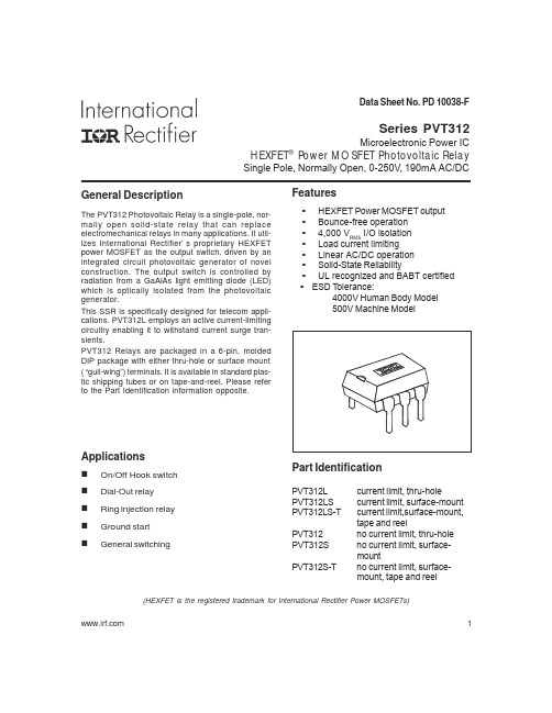
Data Sheet No. PD 10038-FSeries PVT312Microelectronic Power ICHEXFET ® Power MOSFET Photovoltaic RelaySingle Pole, Normally Open, 0-250V, 190mA AC/DCGeneral DescriptionThe PVT312 Photovoltaic Relay is a single-pole, nor-mally open solid-state relay that can replace electromechanical relays in many applications. It util-izes International Rectifier’s proprietary HEXFET power MOSFET as the output switch, driven by an integrated circuit photovoltaic generator of novel construction. The output switch is controlled by radiation from a GaAlAs light emitting diode (LED)which is optically isolated from the photovoltaic generator.This SSR is specifically designed for telecom appli-cations. PVT312L employs an active current-limiting circuitry enabling it to withstand current surge tran-sients.PVT312 Relays are packaged in a 6-pin, molded DIP package with either thru-hole or surface mount ( “gull-wing”) terminals. It is available in standard plas-tic shipping tubes or on tape-and-reel. Please refer to the Part Identification information opposite.(HEXFET is the registered trademark for International Rectifier Power MOSFETs)Applications!On/Off Hook switch !Dial-Out relay !Ring injection relay !Ground start !General switchingPart IdentificationPVT312L current limit, thru-holePVT312LS current limit, surface-mount PVT312LS-T current limit,surface-mount,tape and reelPVT312no current limit, thru-hole PVT312S no current limit, surface-mountPVT312S-Tno current limit, surface-mount, tape and reelFeatures"HEXFET Power MOSFET output "Bounce-free operation "4,000 V RMS I/O isolation "Load current limiting "Linear AC/DC operation "Solid-State Reliability"UL recognized and BABT certified "ESD Tolerance:4000V Human Body Model500V Machine Model 1Series PVT312GENERAL CHARACTERISTICSALL MODELSMinimum Dielectric Strength, Input-Output4000V RMS Minimum Insulation Resistance, Input-Output @T A =+25°C, 50%RH, 100V DC 1012ΩMaximum Capacitance, Input-Output1.0pF Maximum Pin Soldering Temperature (10 seconds maximum)+260°C Ambient Temperature Range:Operating-40 to +85°CStorage-40 to +100OUTPUT CHARACTERISTICSPVT312L PVT312Operating Voltage Range0 to ±250V (DC or AC peak)Maximum Load Current @ T A =+40°C, 5mA Control (see figures 1 and 2)A Connection 170190mA (AC or DC)B Connection 190210mA (DC)C Connection300320mA (DC)Maximum On-State Resistance @T A =+25°C for 50mA pulsed load5mA Control (see figure4)A Connection 1510ΩB Connection 8 5.5ΩC Connection4.253ΩMaximum Off-State Leakage @T A =+25°C, ±250V (see figure 5) 1.0µACurrent Limit @T A =+25°C, 5mA ControlConnection:A C Minimum 190330n/a mA Maximum300560n/amA Maximum Turn-On Time @T A =+25°C (see figure 7)3.0ms for 50mA, 100 V DC load, 5mA ControlMaximum Turn-Off Time @T A =+25°C (See Fig. 6)0.5ms For 50mA, 100 V DC load, 5mA ControlMaximum Output Capacitance @ 50V DC50pFINPUT CHARACTERISTICSPart NumbersUnitsMinimum Control Current (see figures 1 and 2)2.0mA Maximum Control Current for Off-State Resistance @ T A =+25°C 0.4mA Control Current Range (Caution: current limit input LED, see figure 6) 2.0 to 25mA Maximum Reverse Voltage7.0VElectrical Specifications (-40°C ≤ T A ≤ +85°C unless otherwise specified )PVT312LPVT312International Rectifier does not recommend the use of this product in aerospace, avionics, military or life support ers of this International Rectifier product in such applications assume all risks of such use and indemnify International Rectifier against all damages resulting from such use.Series PVT312 3Connection DiagramsFigure 3. Linearity CharacteristicsFigure 4. Typical Normalized On-ResistanceAmbient Temperature (deg. C)2.52.01.51.00.5Voltage Drop (Vdd)Figure 1. Typical Current Derating CurvesFigure 2. Typical Current Derating CurvesAmbient Temperature (deg. C)Ambient Temperature (deg. C)Series PVT3124Vdd, Drain to Drain Voltage (V)Delay Time (microseconds)Figure 7. Typical Delay Times Figure 8. Delay Time DefinitionsFigure 9. Typical Output CapacitanceFigure 5. Typical Normalized Off-State L eakage Figure 6. Input Characteristics (Current Controlled)LED Forward Voltage Drop (Volts D16201284Ambient Temperature (deg. C)Case Outlines233 Kansas St., El Segundo, California 90245 Tel: (310) 252-7105Data and specifications subject to change without notice. 10/17/20035。
UPC1093T-E1中文资料
Pd - Power Dissipation - W
µPC1093
Pd vs TA ( II )
(with 16 cm2×0.7 mm ceramic substrate) 2.0
µPC1093T 62.5 °C/W
1.6
1.2
0.8
µ PC1093TA
245 °C/W
0.4
(with 75 mm2×0.7 mm ceramic
DATA SHEET
BIPOLAR ANALOG INTEGRATED CIRCUIT
µPC1093
ADJUSTABLE PRECISION SHUNT REGULATORS
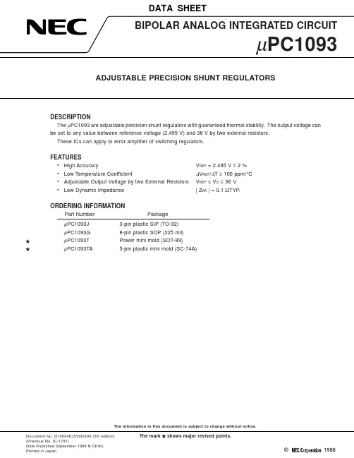
DESCRIPTION The µPC1093 are adjustable precision shunt regulators with guaranteed thermal stability. The output voltage can
100 k
1M
f - Frequency - Hz
Av vs f
40
Av - Voltage Gain - dB
20 220 Ω
IK νo νin
10 kΩ
0 ~ 10 kΩ
–20 1k
(IK = 10 mA)
10 k
100 k
1M
f - Frequency - Hz
10 M
6
VREF - Reference Voltage - V VIN - Input Voltage - V
The information in this document is subject to change without notice.
AQH1223A;AQH1223;AQH3223A;AQH3223;AQH3213A;中文规格书,Datasheet资料
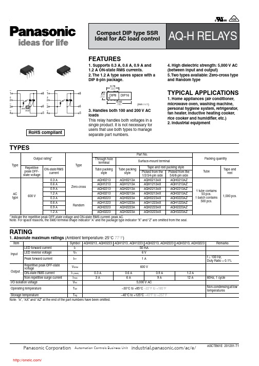
Panasonic Corporation Automation Controls Business Unit /ac/e/ASCTB61E 201201-T1TYPES*Indicate the repetitive peak OFF-state voltage and ON-state RMS current: peak AC.Note:For space reasons, the SMD terminal shape indicator “A” and the package type indicator “X” and “Z” are omitted from the seal.RATING1. Absolute maximum ratings (Ambient temperature: 25°C 77°F )Note:“A”, “AX” and “AZ” at the end of the part numbers have been omitted.T ypeOutput rating*T ypePart No.Packing quantityThrough hole terminal Surface-mount terminalRepetitive peak OFF-state voltageON-state RMScurrentTube packingstyle T ube packingstyle T ape and reel packing style T ubeT ape and reelPicked from the 1/2/3/4-pin side Picked from the 5/6/8-pin side AC type600 V 0.3 A Zero-crossAQH0213AQH0213A AQH0213AX AQH0213AZ 1 tube contains50 pcs.1 batch contains500 pcs.1,000 pcs.0.6 A AQH1213AQH1213A AQH1213AX AQH1213AZ 0.9 AAQH2213AQH2213A AQH2213AX AQH2213AZ 1.2 A AQH3213AQH3213A AQH3213AX AQH3213AZ 0.3 A RandomAQH0223AQH0223A AQH0223AX AQH0223AZ 0.6 A AQH1223AQH1223A AQH1223AX AQH1223AZ 0.9 A AQH2223AQH2223A AQH2223AX AQH2223AZ 1.2 AAQH3223AQH3223AAQH3223AXAQH3223AZItemSymbol AQH0213, AQH0223AQH1213, AQH1223AQH2213, AQH2223AQH3213, AQH3223RemarksInputLED forward current I F 50 mA LED reverse voltage V R6 VPeak forward current I FP 1 A f = 100 Hz,Duty Ratio = 0.1%OutputRepetitive peak OFF-state voltageV DRM 600 VON-state RMS currentI T (RMS)0.3 A 0.6 A 0.9 A 1.2 A Non-repetitive surge currentI TSM 3 A6 A9 A12 A60Hz, 1 cycleI/O isolation voltage V iso 5,000 V ACOperating temperature T opr –30°C to +85°C –22°F to +185°F Non-condensing at low temperaturesStorage temperatureT stg–40°C to +125°C –40°F to +257°FRoHS compliantFEATURES1. Supports 0.3 A, 0.6 A, 0.9 A and 1.2 A ON-state RMS currents.2. The 1.2 A type saves space with a DIP 8-pin package.3. Handles both 100 and 200 V AC loadsThis relay handles both voltages in a single product. It is not necessary for users that use both types to manage separate part numbers.4. High dielectric strength: 5,000 V AC (between input and output)5. Two types available: Zero-cross type and Random typeTYPICAL APPLICATIONS1. Home appliances (air conditioner, microwave oven, washing machine, personal hygiene system, refrigerator, fan heater, inductive heating cooker, rice cooker and humidifier, etc.)2. Industrial equipment(mm inch )/Panasonic Corporation Automation Controls Business Unit /ac/e/AQ-HASCTB61E 201201-T1REFERENCE DATA1. ON-state RMS current vs. Ambient temperature characteristicsAllowable ambient temperature:–30°C to +85°C –22°F to +185°F2. Peak ON-state voltage vs. Ambient temperature characteristicsLED current: 10 mA; ON current: Max.Measured portion: between terminals 6 and 83. T rigger LED current vs. Ambient temperature characteristicsLoad voltage: 6 V DC;Load resistance: 100ΩAmbient temperature, °C O N -s t a t e R M S c u r r e n t , AAmbient temperature, °C P e a k O N -s t a t e v o l t a g e , VAmbient temperature, °C020********–30–40–20264810T r i g g e r L E D c u r r e n t , m A4. LED dropout voltage vs. Ambient temperature characteristicsLED current: 10 to 50 mA5. T urn on time vs. LED current characteristicsLoad voltage: 6 V DC; Load resistance: 100ΩMeasured portion: between terminals 6 and 86. Repetitive peak OFF-state current vs. Load voltage characteristicsAmbient temperature: 25°C 77°F ; Measured portion: between terminals 6 and 8; LED current: 0 mAAmbient temperature, °C 020********–30–40–201.11.311.21.41.550mA30mA 20mA10mAL E D d r o p o u t v o l t a g e , VTrigger LED current, mA 010********20604080100T u r n o n t i m e , µsLoad voltage, V2040608010010–1010–910–810–710–610–510–410–3R e p e t i t i v e p e a k O F F -s t a t e c u r r e n t , A/Panasonic Corporation Automation Controls Business Unit /ac/e/AQ-HASCTB61E 201201-T1DIMENSIONS (mm inch )SCHEMATIC AND WIRING DIAGRAMS1F L L 7. Hold current vs. Ambient temperature characteristics8. Zero-cross voltage vs. Ambient temperature characteristicsLED current: 10 mAAmbient temperature, °C H o l d c u r r e n t , m AAmbient temperature, °CZ e r o -c r o s s v o l t a g e , VThe CAD data of the products with a CAD Data mark can be downloaded from: /ac/e/Through hole terminal typeExternal dimensions T erminal thickness: 0.25 .010General tolerance: ±0.1 ±.004PC board pattern (BOTTOM VIEW)T olerance: ±0.1 ±.004°°.100.100.100Surface mount terminal typeExternal dimensions T erminal thickness: 0.25 .010General tolerance: ±0.1 ±.004Recommended mounting pad (TOP VIEW)0.2.008.100.100.100.100.100.100T olerance: ±0.1 ±.004CAD Data/分销商库存信息:PANASONICAQH1223A AQH1223AQH3223A AQH3223AQH3213A AQH3213 AQH1213AZ AQH1223AX AQH1223AZ AQH1213A AQH1213AQH2213 AQH2213A AQH2223AQH2223A。
TIP131;TIP131G;TIP132G;中文规格书,Datasheet资料
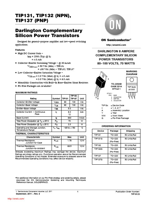
DUTY CYCLE, D = t1/t2
0.5 1.0 2.0
5.0 10 20
t, TIME (ms)
Figure 3. Thermal Response
50 100 200
500 1.0 k
r(t), TRANSIENT THERMAL RESISTANCE (NORMALIZED)
BASE COLLECTOR EMITTER COLLECTOR
TIP13xG AYWW
TIP13x x A Y WW G
= Device Code = 1, 2, or 7 = Assembly Location = Year = Work Week = Pb−Free Package
ORDERING INFORMATION
DARLINGTON 8 AMPERE COMPLEMENTARY SILICON
POWER TRANSISTORS 80−100 VOLTS, 70 WATTS
MARKING DIAGRAM
4
1 2 3
220AB CASE 221A
STYLE 1
STYLE 1: PIN 1. 2. 3. 4.
IB PD PD TJ, Tstg
300 70 2.0 – 65 to + 150
mAdc W W °C
THERMAL CHARACTERISTICS
Characteristic
Symbol
Max
Unit
Thermal Resistance, Junction−to−Case
RqJC
1.78
°C/W
--- 2.04
STYLE 1: PIN 1. BASE 2. COLLECTOR 3. EMITTER 4. COLLECTOR
IDCP3114ER100M;IDCP3114ER101M;IDCP3114ER121M;IDCP3114ER220M;IDCP3114ER271M;中文规格书,Datasheet资料
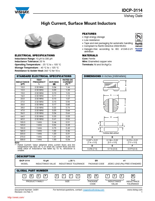
Document Number: 34091For technical questions, contact: magnetics@Revision: 24-Feb-111High Current, Surface Mount InductorsIDCP-3114Vishay DaleFEATURES•High energy storage •Low resistance•Tape and reel packaging for automatic handling •Compliant to RoHS Directive 2002/95/EC•Halogen-free according to IEC 61249-2-21definitionELECTRICAL SPECIFICATIONSInductance Range: 10 μH to 330 μH Inductance Tolerance: 20 %Operating Temperature: - 25 °C to + 105 °C Storage Temperature: - 40 °C to + 125 °C Resistance to Solder Heat: 260 °C for 10 sMATERIALSCore: FerriteWire: Enamelled copper wire Terminals: Ni and Sn/Ag/CuNote(1)Rated Current: Value obtained when current flows and the temperature has risen 40 °C or when DC current flows and the initial value of inductance has fallen by 10 %, whichever is smaller.STANDARD ELECTRICAL SPECIFICATIONSINDUCTANCE(μH)TEST FREQUENCYL DCR MAX.( )RATED DC CURRENT (A) (1)10.0 2.52 MHz 0.08 1.4412.0 2.52 MHz 0.09 1.3915.0 2.52 MHz 0.10 1.2418.0 2.52 MHz 0.11 1.1222.0 2.52 MHz 0.13 1.0727.0 2.52 MHz 0.150.9433.0 2.52 MHz 0.170.8539.0 2.52 MHz 0.220.7447.0 2.52 MHz 0.250.6856.0 2.52 MHz 0.280.6468.0 2.52 MHz 0.330.5982.0 2.52 MHz 0.410.54100.0 1 kHz 0.480.51120.0 1 kHz 0.540.49150.0 1 kHz 0.750.40180.0 1 kHz 1.020.36220.0 1 kHz 1.200.31270.0 1 kHz 1.310.29330.01 kHz1.500.28DESCRIPTIONIDCP-311410 μH± 20 %ERe1MODELINDUCTANCE VALUEINDUCTANCE TOLERANCEPACKAGE CODEJEDEC LEAD (Pb)-FREE STANDARDGLOBAL PART NUMBERIDCP3114ER100M PRODUCT FAMILYSIZEPACKAGE CODEINDUCTANCEVALUEINDUCTANCE TOLERANCELegal Disclaimer Notice VishayDisclaimerALL PRODU CT, PRODU CT SPECIFICATIONS AND DATA ARE SU BJECT TO CHANGE WITHOU T NOTICE TO IMPROVE RELIABILITY, FUNCTION OR DESIGN OR OTHERWISE.Vishay Intertechnology, Inc., its affiliates, agents, and employees, and all persons acting on its or their behalf (collectively,“Vishay”), disclaim any and all liability for any errors, inaccuracies or incompleteness contained in any datasheet or in any other disclosure relating to any product.Vishay makes no warranty, representation or guarantee regarding the suitability of the products for any particular purpose or the continuing production of any product. To the maximum extent permitted by applicable law, Vishay disclaims (i) any and all liability arising out of the application or use of any product, (ii) any and all liability, including without limitation special, consequential or incidental damages, and (iii) any and all implied warranties, including warranties of fitness for particular purpose, non-infringement and merchantability.Statements regarding the suitability of products for certain types of applications are based on Vishay’s knowledge of typical requirements that are often placed on Vishay products in generic applications. Such statements are not binding statements about the suitability of products for a particular application. It is the customer’s responsibility to validate that a particular product with the properties described in the product specification is suitable for use in a particular application. Parameters provided in datasheets and/or specifications may vary in different applications and performance may vary over time. All operating parameters, including typical parameters, must be validated for each customer application by the customer’s technical experts. Product specifications do not expand or otherwise modify Vishay’s terms and conditions of purchase, including but not limited to the warranty expressed therein.Except as expressly indicated in writing, Vishay products are not designed for use in medical, life-saving, or life-sustaining applications or for any other application in which the failure of the Vishay product could result in personal injury or death. Customers using or selling Vishay products not expressly indicated for use in such applications do so at their own risk and agree to fully indemnify and hold Vishay and its distributors harmless from and against any and all claims, liabilities, expenses and damages arising or resulting in connection with such use or sale, including attorneys fees, even if such claim alleges that Vishay or its distributor was negligent regarding the design or manufacture of the part. Please contact authorized Vishay personnel to obtain written terms and conditions regarding products designed for such applications.No license, express or implied, by estoppel or otherwise, to any intellectual property rights is granted by this document or by any conduct of Vishay. Product names and markings noted herein may be trademarks of their respective owners.Material Category PolicyVishay Intertechnology, Inc. hereb y certifies that all its products that are identified as RoHS-Compliant fulfill the definitions and restrictions defined under Directive 2011/65/EU of The European Parliament and of the Council of June 8, 2011 on the restriction of the use of certain hazardous substances in electrical and electronic equipment (EEE) - recast, unless otherwise specified as non-compliant.Please note that some Vishay documentation may still make reference to RoHS Directive 2002/95/EC. We confirm that all the products identified as being compliant to Directive 2002/95/EC conform to Directive 2011/65/EU.Revision: 12-Mar-121Document Number: 91000分销商库存信息:VISHAYIDCP3114ER100M IDCP3114ER101M IDCP3114ER121M IDCP3114ER220M IDCP3114ER271M IDCP3114ER330M IDCP3114ER331M IDCP3114ER470M IDCP3114ER820M。
MCH6613-TL-E;中文规格书,Datasheet资料
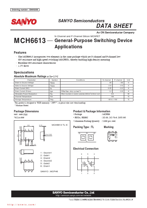
Features• The MCH6613 incorporates two elements in the same package which are N-channel and P-channel low ON resistance and high-speed switching MOSFETs, thereby enabling high-density mounting • Excellent ON-resistance characteristic • 1.5V driveSpeci fi cationsAbsolute Maximum Ratingsat Ta=25°CParameterSymbol Conditions N-channelP-channelUnit Drain-to-Source Voltage V DSS30--30V Gate-to-Source Voltage V GSS ±10±10V Drain Current (DC)I D 0.35--0.2A Drain Current (Pulse)I DP PW ≤10μs, duty cycle ≤1%1.4--0.8A Allowable Power Dissipation P D When mounted on ceramic substrate (900mm 2×0.8mm) 1unit0.8W Channel Temperature Tch 150°C Storage TemperatureTstg--55 to +150°CThis product is designed to “ESD immunity < 200V *”, so please take care when handling.* Machine ModelPackage Dimensionsunit : mm (typ)7022A-006MCH6613N-Channel and P-Channel Silicon MOSFETGeneral-Purpose Switching Device ApplicationsProduct & Package Information• Package : MCPH6• JEITA, JEDEC : SC-88, SC-70-6, SOT-363• Minimum Packing Quantity : 3,000 pcs./reelPacking Type : TL MarkingElectrical ConnectionTLFMLOT No.LOT No.654Electrical Characteristics at Ta=25°CParameter Symbol ConditionsRatingsUnit min typ max[N-channel]Drain-to-Source Breakdown Voltage V(BR)DSS I D=1mA, V GS=0V30V Zero-Gate Voltage Drain Current I DSS V DS=30V, V GS=0V1μA Gate-to-Source Leakage Current I GSS V GS=±8V, V DS=0V±10μA Cutoff Voltage V GS(off)V DS=10V, I D=100μA0.4 1.3V Forward Transfer Admittance| yfs |V DS=10V, I D=80mA150220mSStatic Drain-to-Source On-State Resistance R DS(on)1I D=80mA, V GS=4V 2.9 3.7ΩR DS(on)2I D=40mA, V GS=2.5V 3.7 5.2ΩR DS(on)3I D=10mA, V GS=1.5V 6.412.8ΩInput Capacitance CissV DS=10V, f=1MHz 7.0pFOutput Capacitance Coss 5.9pF Reverse Transfer Capacitance Crss 2.3pFTurn-ON Delay Time t d(on)See specifi ed Test Circuit.19nsRise Time t r65ns Turn-OFF Delay Time t d(off) 155ns Fall Time t f120nsTotal Gate Charge QgV DS=10V, V GS=10V, I D=150mA 1.58nCGate-to-Source Charge Qgs0.26nC Gate-to-Drain “Miller” Charge Qgd0.31nC Diode Forward Voltage V SD I S=150mA, V GS=0V0.87 1.2V [P-channel]Drain-to-Source Breakdown Voltage V(BR)DSS I D=--1mA, V GS=0V--30V Zero-Gate Voltage Drain Current I DSS V DS=--30V, V GS=0V--1μA Gate-to-Source Leakage Current I GSS V GS=±8V, V DS=0V±10μA Cutoff Voltage V GS(off)V DS=--10V, I D=--100μA--0.4--1.4V Forward Transfer Admittance| yfs |V DS=--10V, I D=--50mA80110mSStatic Drain-to-Source On-State Resistance R DS(on)1I D=--50mA, V GS=--4V810.4ΩR DS(on)2I D=--30mA, V GS=--2.5V1115.4ΩR DS(on)3I D=--1mA, V GS=--1.5V2754ΩInput Capacitance CissV DS=--10V, f=1MHz 7.5pFOutput Capacitance Coss 5.7pF Reverse Transfer Capacitance Crss 1.8pFTurn-ON Delay Time t d(on)See specifi ed Test Circuit.24nsRise Time t r55ns Turn-OFF Delay Time t d(off) 120ns Fall Time t f130nsTotal Gate Charge QgV DS=--10V, V GS=--10V, I D=--100mA 1.43nCGate-to-Source Charge Qgs0.18nC Gate-to-Drain “Miller” Charge Qgd0.25nC Diode Forward Voltage V SD I S=--100mA, V GS=0V--0.83--1.2VSwitching Time Test Circuit[N-channel] [P-channel]Ordering InformationDevicePackage Shipping memo MCH6613-TL-EMCPH63,000pcs./reelPb FreeP ΩV =15VV OUTP .GΩV = --15VV OUTDrain-to-Source V oltage, V DS -- VD r a i n C u r r e n t , I D -- AD r a i n C u r r e n t , I D -- ADrain-to-Source V oltage, V DS -- VD r a i n C u r r e n t , I D -- AD r a i n C u r r e n t , I D -- A00.020.060.040.080.100.120.140.1600.150.100.050.300.250.20IT00029IT00077St a t i c D r a i n -t o -S o u r c e O n -S t a t e R e s i s t a n c e , R D S (o n ) -- ΩDrain Current, I D -- AS t a t i c D r a i n -t o -S o u r c e O n -S t a t e R e s i s t a n c e , R D S (o n ) -- ΩS t a t i c D r a i n -t o -S o u r c e O n -S t a t e R e s i s t a n c e , R D S (o n ) --ΩDrain Current, I D -- AS t a t i c D r a i n -t o -S o u r c e O n -S t a t e R e s i s t a n c e , R D S(o n ) -- Ω0.010.1101.01.00.0010.0110010IT00033--0.011.0--0.110100--0.0001--0.001100010010IT00081S t a t i c D r a i n -t o -S o u r c e O n -S t a t e R e s i s t a n c e , R D S (o n ) -- ΩDrain Current, I D -- AS t a t i c D r a i n -t o -S o u r c e O n -S t a t e R e s i s t a n c e , R D S (o n ) -- ΩDrain Current, I D -- A0.010.1101.0IT00032--0.011.0--0.110010IT00080S t a t i c D r a i n -t o -S o u r c e O n -S t a t e R e s i s t a n c e , R D S (o n ) -- ΩGate-to-Source V oltage, V GS -- VS t a t i c D r a i n -t o -S o u r c e O n -S t a t e R e s i s t a n c e , R D S (o n ) -- ΩGate-to-Source V oltage, V GS -- VIT00031IT000790.010.11.075327532Diode Forward V oltage, V SD -- VS o u r c e C u r r e n t , I S -- A0.01100.11000100S w i t c h i n g T i m e , S W T i m e -- n sIT00037--0.01--0.15327532Diode Forward V oltage, V SD -- VS o u r c e C u r r e n t , I S -- AIT00085--0.0110--0.11000100S w i t c h i n g T i m e , S W T i m e -- n sDrain Current, I D -- ADrain Current, I D -- A0.010.010.10.11.0IT00036[Pch]--0.010.01--0.11.00.1IT00084S t a t i c D r a i n -t o -S o u r c e O n -S t a t e R e s i s t a n c e , R D S (o n ) -- ΩAmbient Temperature, Ta -- °CS t a t i c D r a i n -t o -S o u r c e O n -S t a t e R e s i s t a n c e , R D S (o n ) -- ΩAmbient Temperature, Ta -- °C1234567IT000354281012141618IT00083F o r w a r d T r a n s f e r A d m i t t a n c e , | y f s | -- SF o r w a r d T r a n s f e r A d m i t t a n c e , | y f s | -- S1.00.10.011.00.60.40.20.8A l l o w a b l e P o w e r D i s s i p at i o n , P D -- WDrain-to-Source V oltage, V DS -- VD r a i n C u r r e n t , I D -- A1.010IT02877--0.01--0.1--1.0--1.0--10Drain-to-Source V oltage, V DS -- VD r a i n C u r r e n t , I D -- AIT02878Total Gate Charge, Qg -- nCG a t e -t o -S o u r c e V o l t a g e , V G S -- VIT00040Total Gate Charge, Qg -- nCG a t e -t o -S o u r c e V o l t a g e , V G S -- VIT000881.010100Drain-to-Source V oltage, V DS -- VC i s s , C o s s , C r s s -- p FCiss, Coss, Crss -- V IT000391.01075327532100Drain-to-Source V oltage, V DS -- VC i s s , C o s s , C r s s -- p FIT00087[Pch]Embossed Taping Speci fi cationMCH6613-TL-EOutline Drawing Land Pattern Example MCH6613-TL-EMass (g)Unit0.008 * For reference mmUnit: mm0.650.650.42.1.6Note on usage : Since the MCH6613 is a MOSFET product, please avoid using this device in the vicinity of highly charged objects.This catalog provides information as of July, 2012. Specifi cations and information herein are subject分销商库存信息: ONSEMIMCH6613-TL-E。
HPLR3103T中文资料
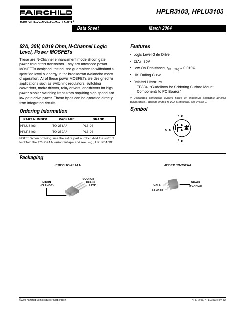
CAUTION: Stresses above those listed in “Absolute Maximum Ratings” may cause permanent damage to the device. This is a stress only rating and operation of the device at these or any other conditions above those indicated in the operational sections of this specification is not implied.
oC/W oC/W oC/W
Source to Drain Diode Specifications
PARAMETER Continuous Source to Drain Current SYMBOL ISD ISDM TEST CONDITIONS MOSFET Symbol Showing The Integral Reverse P-N Junction Diode
oC oC
Drain to Source Voltage (Note 1) . . . . . . . . . . . . . . . . . . . . . . . . . . . . . . . . . . . . . . . . . . VDSS Drain to Gate Voltage (RGS = 20kΩ) (Note 1) . . . . . . . . . . . . . . . . . . . . . . . . . . . . . . . . VDGR Gate to Source Voltage . . . . . . . . . . . . . . . . . . . . . . . . . . . . . . . . . . . . . . . . . . . . . . . . . . VGS Continuous Drain Current . . . . . . . . . . . . . . . . . . . . . . . . . . . . . . . . . . . . . . . . . . . . . . . . . . ID Pulsed Drain Current (Note 2) . . . . . . . . . . . . . . . . . . . . . . . . . . . . . . . . . . . . . . . . . . . . . .IDM Single Pulse Avalanche Energy (Note 4) . . . . . . . . . . . . . . . . . . . . . . . . . . . . . . . . . . . . . EAS Power Dissipation . . . . . . . . . . . . . . . . . . . . . . . . . . . . . . . . . . . . . . . . . . . . . . . . . . . . . . . PD Derate Above 25oC . . . . . . . . . . . . . . . . . . . . . . . . . . . . . . . . . . . . . . . . . . . . . . . . . . . . . . . Operating and Storage Temperature . . . . . . . . . . . . . . . . . . . . . . . . . . . . . . . . . . . . TJ, TSTG Maximum Temperature for Soldering Leads at 0.063in (1.6mm) from Case for 10s. . . . . . . . . . . . . . . . . . . . . . . . . . . . . . . . . . TL Package Body for 10s, See Techbrief 334 . . . . . . . . . . . . . . . . . . . . . . . . . . . . . . . . . . Tpkg
AP4313中文规格书,AP4313KTR-G1中文datasheet翻译

2.650(0.104) 2.950(0.116) 1.500(0.059) 1.700(0.067)
引脚1含有圆点标注
1
2
3
0.950(0.037)典型
1.800(0.071) 2.000(0.079)
0.700(0.028)参考值
0.000(0.000) 0.150(0.006)
GND
R5
ICTRL
VSENSE
R1
R6 500
Rss
VOUT
= VREF
× R1+ R2 R1
(V)
限流电流 = VSENSE (A) RSS
图 10. AP4313的典型应用1
VOUT+ IL Load
VOUT-
2010年5月 版本2. 0
BCD 新进半导体制造有限公司 8
恒压恒流控制器 典型应用 (续页)
产品规格书 AP4313
I (mA)
OS
I (mA)
CC
60
50
40
30
20
V =12V
CC
V =5V
CC
V =2.5V
10
CC
0
-40
-20
0
20
40
60
80
100
120
环境温度(oC)
图 8. 输出引脚的短路电流 – 环境温度 关系图
1.4
1.0
0.8
0.6
0.4
0.2
0.0
-40
-20
0
CC
V =5V CC
BCD 新进半导体制造有限公司 1
恒压恒流控制器 引脚信息
EG3113 芯片数据手册说明书
版本变更记录目录1. 特性 (1)2. 描述 (1)3. 应用领域 (1)4. 引脚 (2)4.1 引脚定义 (2)4.2 引脚描述 (2)5. 结构框图 (3)6. 典型应用电路 (3)7. 电气特性 (4)7.1 极限参数 (4)7.2 典型参数 (5)7.3 开关时间特性及死区时间波形图 (6)8. 应用设计 (7)8.1 Vcc端电源电压 (7)8.2 输入逻辑信号要求和输出驱动器特性 (7)8.3 自举电路 (8)9. 封装尺寸 (9)9.1 SO8封装尺寸 (9)9.2 DFN8封装尺寸 (9)EG3113芯片数据手册V1.01. 特性⏹高端悬浮自举电源设计,耐压可达600V⏹适应5V、3.3V输入电压⏹最高频率支持500KHZ⏹低端VCC电压范围2.8V-20V⏹输出电流能力I O+/- 1A/1.5A⏹内建死区控制电路⏹自带闭锁功能,彻底杜绝上、下管输出同时导通⏹HIN输入通道高电平有效,控制高端HO输出⏹LIN输入通道低电平有效,控制低端LO输出⏹外围器件少⏹静态电流小于5uA,非常适合电池场合⏹封装形式:SOP-8,DFN82. 描述EG3113是一款高性价比的大功率MOS管、IGBT管栅极驱动专用芯片,内部集成了逻辑信号输入处理电路、死区时控制电路、闭锁电路、电平位移电路、脉冲滤波电路及输出驱动电路,专用于无刷电机控制器中的驱动电路。
EG3113高端的工作电压可达600V,低端Vcc的电源电压范围宽2.8V~20V,静态功耗小于5uA。
该芯片具有闭锁功能防止输出功率管同时导通,输入通道H IN内建了一个200K下拉电阻,LIN内建了上拉5V 高电位,在输入悬空时使上、下功率MOS管处于关闭状态,输出电流能力I O+/- 1/1.5A,采用SOP8封装。
3. 应用领域⏹移动电源高压快充开关电源⏹电动车控制器⏹变频水泵控制器⏹600V降压型开关电源⏹无刷电机驱动器⏹高压Class-D类功放4. 引脚4.1 引脚定义IN IN图4-1. EG3113管脚定义4.2 引脚描述5. 结构框图LOGNDVccHOVS VB图5-1. EG3113内部电路图6. 典型应用电路+12V+600VOUT图6-1. EG3113典型应用电路图7. 电气特性7.1 极限参数注:超出所列的极限参数可能导致芯片内部永久性损坏,在极限的条件长时间运行会影响芯片的可靠性。
1SV323(TPH3,F);中文规格书,Datasheet资料
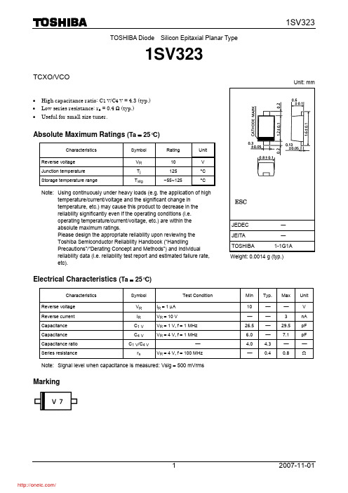
2007-11-011TOSHIBA Diode Silicon Epitaxial Planar Type1SV323TCXO/VCO• High capacitance ratio: C 1 V /C 4 V = 4.3 (typ.)• Low series resistance: r s = 0.4 Ω (typ.)• Useful for small size tuner.Absolute Maximum Ratings (Ta = 25°C) Characteristics Symbol RatingUnitReverse voltageV R 10 V Junction temperatureT j 125 °C Storage temperature range T stg −55~125 °CNote: Using continuously under heavy loads (e.g. the application of hightemperature/current/voltage and the significant change intemperature, etc.) may cause this product to decrease in thereliability significantly even if the operating conditions (i.e.operating temperature/current/voltage, etc.) are within theabsolute maximum ratings.Please design the appropriate reliability upon reviewing theToshiba Semiconductor Reliability Handbook (“HandlingPrecautions”/“Derating Concept and Methods”) and individualreliability data (i.e. reliability test report and estimated failure rate,etc).Electrical Characteristics (Ta = 25°C)Characteristics Symbol Test Condition Min Typ. Max UnitReverse voltageV R I R = 1 μA 10 ⎯ ⎯ V Reverse current I R V R = 10 V⎯ ⎯ 3 nA Capacitance C 1 V V R = 1 V, f = 1 MHz26.5 ⎯ 29.5pF Capacitance C 4 VV R = 4 V, f = 1 MHz 6.0 ⎯ 7.1 pF Capacitance ratioC 1 V /C 4 V ⎯ 4.0 4.3 ⎯ ⎯ Series resistance r s V R = 4 V, f = 100 MHz ⎯ 0.4 0.8 Ω Note: Signal level when capacitance is measured: Vsig = 500 mVrmsMarkingUnit: mm JEDEC ― JEITA ― TOSHIBA 1-1G1A Weight: 0.0014 g (typ.)/2007-11-012h t t p ://o n e i c .c o m /2007-11-013RESTRICTIONS ON PRODUCT USE• Toshiba Corporation, and its subsidiaries and affiliates (collectively “TOSHIBA”), reserve the right to make changes to the information in this document, and related hardware, software and systems (collectively “Product”) without notice.• This document and any information herein may not be reproduced without prior written permission from TOSHIBA. Even with TOSHIBA’s written permission, reproduction is permissible only if reproduction is without alteration/omission.• Though TOSHIBA works continually to improve Product’s quality and reliability, Product can malfunction or fail. Customers areresponsible for complying with safety standards and for providing adequate designs and safeguards for their hardware, software and systems which minimize risk and avoid situations in which a malfunction or failure of Product could cause loss of human life, bodily injury or damage to property, including data loss or corruption. Before creating and producing designs and using, customers must also refer to and comply with (a) the latest versions of all relevant TOSHIBA information, including without limitation, this document, the specifications, the data sheets and application notes for Product and the precautions and conditions set forth in the “TOSHIBA Semiconductor Reliability Handbook” and (b) the instructions for the application that Product will be used with or for. Customers are solely responsible for all aspects of their own product design or applications, including but not limited to (a) determining theappropriateness of the use of this Product in such design or applications; (b) evaluating and determining the applicability of any information contained in this document, or in charts, diagrams, programs, algorithms, sample application circuits, or any other referenced documents; and (c) validating all operating parameters for such designs and applications. TOSHIBA ASSUMES NO LIABILITY FOR CUSTOMERS’ PRODUCT DESIGN OR APPLICATIONS.• Product is intended for use in general electronics applications (e.g., computers, personal equipment, office equipment, measuring equipment, industrial robots and home electronics appliances) or for specific applications as expressly stated in this document. Product is neither intended nor warranted for use in equipment or systems that require extraordinarily high levels of quality and/or reliability and/or a malfunction or failure of which may cause loss of human life, bodily injury, serious property damage or serious public impact (“Unintended Use”). Unintended Use includes, without limitation, equipment used in nuclear facilities, equipment used in the aerospace industry, medical equipment, equipment used for automobiles, trains, ships and other transportation, traffic signaling equipment, equipment used to control combustions or explosions, safety devices, elevators and escalators, devices related to electric power, and equipment used in finance-related fields. Do not use Product for Unintended Use unless specifically permitted in this document.• Do not disassemble, analyze, reverse-engineer, alter, modify, translate or copy Product, whether in whole or in part.• Product shall not be used for or incorporated into any products or systems whose manufacture, use, or sale is prohibited under any applicable laws or regulations.• The information contained herein is presented only as guidance for Product use. No responsibility is assumed by TOSHIBA for any infringement of patents or any other intellectual property rights of third parties that may result from the use of Product. No license to any intellectual property right is granted by this document, whether express or implied, by estoppel or otherwise.• ABSENT A WRITTEN SIGNED AGREEMENT, EXCEPT AS PROVIDED IN THE RELEVANT TERMS AND CONDITIONS OF SALE FOR PRODUCT, AND TO THE MAXIMUM EXTENT ALLOWABLE BY LAW, TOSHIBA (1) ASSUMES NO LIABILITYWHATSOEVER, INCLUDING WITHOUT LIMITATION, INDIRECT, CONSEQUENTIAL, SPECIAL, OR INCIDENTAL DAMAGES OR LOSS, INCLUDING WITHOUT LIMITATION, LOSS OF PROFITS, LOSS OF OPPORTUNITIES, BUSINESS INTERRUPTION AND LOSS OF DATA, AND (2) DISCLAIMS ANY AND ALL EXPRESS OR IMPLIED WARRANTIES AND CONDITIONS RELATED TO SALE, USE OF PRODUCT, OR INFORMATION, INCLUDING WARRANTIES OR CONDITIONS OF MERCHANTABILITY, FITNESS FOR A PARTICULAR PURPOSE, ACCURACY OF INFORMATION, OR NONINFRINGEMENT.• Do not use or otherwise make available Product or related software or technology for any military purposes, including without limitation, for the design, development, use, stockpiling or manufacturing of nuclear, chemical, or biological weapons or missile technology products (mass destruction weapons). Product and related software and technology may be controlled under theJapanese Foreign Exchange and Foreign Trade Law and the U.S. Export Administration Regulations. Export and re-export of Product or related software or technology are strictly prohibited except in compliance with all applicable export laws and regulations.• Please contact your TOSHIBA sales representative for details as to environmental matters such as the RoHS compatibility of Product. Please use Product in compliance with all applicable laws and regulations that regulate the inclusion or use of controlled substances, including without limitation, the EU RoHS Directive. TOSHIBA assumes no liability for damages or losses occurring as a result of noncompliance with applicable laws and regulations./分销商库存信息: TOSHIBA1SV323(TPH3,F)。
3123中文资料
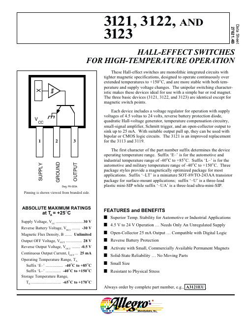
These Hall-effect switches are monolithic integrated circuits with tighter magnetic specifications, designed to operate continuously over extended temperatures to +150°C, and are more stable with both tem-perature and supply voltage changes. The unipolar switching character-istic makes these devices ideal for use with a simple bar or rod magnet.The three basic devices (3121, 3122, and 3123) are identical except for magnetic switch points.Each device includes a voltage regulator for operation with supply voltages of 4.5 voltas to 24 volts, reverse battery protection diode,quadratic Hall-voltage generator, temperature compensation circuitry,small-signal amplifier, Schmitt trigger, and an open-collector output to sink up to 25 mA. With suitable output pull up, they can be used with bipolar or CMOS logic circuits. The 3121 is an improved replacement for the 3113 and 3119.The first character of the part number suffix determines the device operating temperature range. Suffix ‘E–’ is for the automotive and industrial temperature range of -40°C to +85°C. Suffix ‘L–’ is for the automotive and military temperature range of -40°C to +150°C. Three package styles provide a magnetically optimized package for mostapplications. Suffix ‘–LT’ is a miniature SOT-89/TO-243AA transistor package for surface-mount applications; suffix ‘–U’ is a three-lead plastic mini-SIP while suffix ‘–UA’ is a three-lead ultra-mini-SIP.HALL-EFFECT SWITCHESFOR HIGH-TEMPERATURE OPERATIONAlways order by complete part number, e.g., A3121EU .FEATURES and BENEFITSI Superior Temp. Stability for Automotive or Industrial Applications I 4.5 V to 24 V Operation … Needs Only An Unregulated Supply I Open-Collector 25 mA Output … Compatible with Digital Logic I Reverse Battery ProtectionI Activate with Small, Commercially Available Permanent Magnets I Solid-State Reliability … No Moving Parts I Small SizeI Resistant to Physical StressData Sheet 27621.4B3121, 3122, AND 31233121, 3122, AND 3123HALL-EFFECT SWITCHES FOR HIGH-TEMPERATUREOPERATION115 Northeast Cutoff, Box 15036Worcester, Massachusetts 01615-0036 (508) 853-5000LimitsCharacteristic Symbol Test ConditionsMin.Typ.Max.Units Supply VoltageV CC Operating 4.5—24VOutput Saturation Voltage V OUT(SAT)I OUT = 20 mA, B > B OP —140400mV Output Leakage Current I OFF V OUT = 24 V, B < B RP —<1.010µA Supply Current I CC B < B RP (Output OFF)— 4.69.0mA Output Rise Time t r R L = 820 Ω, C L = 20 pF —0.04 2.0µs Output Fall Timet fR L = 820 Ω, C L = 20 pF—0.182.0µsELECTRICAL CHARACTERISTICS over operating temperature range, at V CC = 12 V.MAGNETIC CHARACTERISTICS in gauss over operating supply voltage range.Part Numbers*A3121A3122A3123Characteristic Min.Typ.Max.Min.Typ.Max.Min.Typ.Max B OP at T A = 25°C250350450280340400250345440over operating temp. range 220350500260340430230345470B RP at T A = 25°C125245380140235330180240300over operating temp. range 80245410120235360160240330B hys at T A = 25°C701051407010514070105140over operating temp. range601051507010514070105140NOTES:Typical values are at T A = +25°C and V CC = 12 V.B OP = operate point (output turns ON); B RP = release point (output turns OFF); B hys = hysteresis (B OP - B RP ).*Complete part number includes a suffix to identify operating temperature range (E- or L-) and package type ( -LT, -U, or -UA).Copyright © 1992, 1999, Allegro MicroSystems, Inc.3121, 3122, AND 3123HALL-EFFECT SWITCHES FOR HIGH-TEMPERATUREOPERATIONSWITCH POINTSOUTPUT SATURATION VOLTAGE* Complete part number includes a suffix denoting operating temperature range (E- or L-) and package type ( -LT, -U, or -UA).TYPICAL OPERATING CHARACTERISTICSAMBIENT TEMPERATURE IN °CDwg. GH-038S W I T C H P O I N T I N G A U S S30040020010000AMBIENT TEMPERATURE IN °CDwg. GH-0400255075100AMBIENT TEMPERATURE IN °C-50Dwg. GH-039-25S U P P L Y C U R R E N T I N m A10152025SUPPLY VOLTAGE IN VOLTSDwg. GH-0415S U P P L Y C U R R E N T I N m A0SUPPLY CURRENTSUPPLY CURRENT3121, 3122, AND 3123HALL-EFFECT SWITCHES FOR HIGH-TEMPERATUREOPERATION115 Northeast Cutoff, Box 15036Worcester, Massachusetts 01615-0036 (508) 853-5000OPERATIONThe output of these devices (pin 3) switches low when the mag-netic field at the Hall sensor exceeds the operate point threshold (B OP ).At this point, the output voltage is V OUT(SAT). When the magnetic field is reduced to below the release point threshold (B RP ), the device output goes high. The difference in the magnetic operate and release points is called the hysteresis (B hys ) of the device. This built-in hysteresis allows clean switching of the output even in the presence of external mechani-cal vibration and electrical noise.APPLICATIONS INFORMATIONHall effect applications information is available in the “Hall-Effect IC Applications Guide”, which can be found in the latest issue of Allegro MicroSystems Data Book AMS-702.CHANGE IN OPERATE POINT10152025SUPPLY VOLTAGE IN VOLTSDwg. GH-04253121, 3122, AND 3123HALL-EFFECT SWITCHES FOR HIGH-TEMPERATUREOPERATIONPACKAGE DESIGNATOR ‘LT’Dimensions in Inches (for reference only)Dimensions in Millimeters (controlling dimensions)0.0140.0170.350.44NOTE: Exact body and lead configuration at vendor's option within limits shown.3121, 3122, AND 3123HALL-EFFECT SWITCHES FOR HIGH-TEMPERATUREOPERATION115 Northeast Cutoff, Box 15036Worcester, Massachusetts 01615-0036 (508) 853-5000°°PACKAGE DESIGNATOR ‘U’Dimensions in Inches Dimensions in Millimeters(controlling dimensions)(for reference only)NOTES: 1.Tolerances on package height and width represent allowable mold offsets.Dimensions given are measured at the widest point (parting line).2.Exact body and lead configuration at vendor’s option within limits shown.3.Height does not include mold gate flash.4.Recommended minimum PWB hole diameter to clear transition area is 0.035" (0.89 mm).5.Where no tolerance is specified, dimension is nominal.Devices in the ‘U’ package areNOT RECOMMENDED FOR NEW DESIGN3121, 3122, AND 3123HALL-EFFECT SWITCHES FOR HIGH-TEMPERATUREOPERATIONPACKAGE DESIGNATOR ‘UA’Dimensions in Inches Dimensions in Millimeters(controlling dimensions)(for reference only)NOTES: 1.Tolerances on package height and width represent allowable mold offsets.Dimensions given are measured at the widest point (parting line).2.Exact body and lead configuration at vendor’s option within limits shown.3.Height does not include mold gate flash.4.Recommended minimum PWB hole diameter to clear transition area is 0.035" (0.89 mm).5.Where no tolerance is specified, dimension is nominal.°°3121, 3122, AND 3123HALL-EFFECT SWITCHES FOR HIGH-TEMPERATUREOPERATION115 Northeast Cutoff, Box 15036Worcester, Massachusetts 01615-0036 (508) 853-5000The products described herein are manufactured under one or more of the following U.S. patents: 5,045,920; 5,264,783; 5,442,283;5,389,889; 5,581,179; 5,517,112; 5,619,137; 5,621,319; 5,650,719;5,686,894; 5,694,038; 5,729,130; 5,917,320; and other patents pending.Allegro MicroSystems, Inc. reserves the right to make, from time to time, such departures from the detail specifications as may be required to permit improvements in the performance, reliability, ormanufacturability of its products. Before placing an order, the user is cautioned to verify that the information being relied upon is current.Allegro products are not authorized for use as critical components in life-support appliances, devices, or systems without express written approval.The information included herein is believed to be accurate andreliable. However, Allegro MicroSystems, Inc. assumes no responsibil-ity for its use; nor for any infringements of patents or other rights of third parties that may result from its use.。
AP4313中文规格书,AP4313KTR-G1中文datasheet翻译

符号 VCC TA
最小 2.5 -40
最大 18 105
单位 V oC
2010年5月 版本2. 0
BCD 新进半导体制造有限公司 4
恒压恒流控制器
电气特性
(VCC=5V, TA=25oC, 除非特别说明。)
参数
符号
条件
总共消耗电流
总供电电流
不包括输出引脚的吸入电流
ICC
图 11. AP4313的典型应用2
VOUT+ IL Load
VOUT-
2010年5月 版本2.0
BCD 新进半导体制造有限公司 9
恒压恒流控制器 典型应用(续页)
产品规格书 AP4313
AP4313
VCC
1.210V
+
VOUT VCTRL
ICTRL
GND VSENSE
R6 500
反馈到原级 R2
0.100(0.004) 0.200(0.008)
0.900(0.035) 1.450(0.057)
1.300(0.051)
MAX
2010年5月 版本2.0
BCD 新进半导体制造有限公司 11
BCD 新进半导体制造有限公司
IMPORTANT NOTICE IMPORTANT NOTICE
总部
M- 总A部IN SITE BBCCDD上S海em新i进co芯nd微u电ct子or有M限a公nu司facturing Limited
中- W国a上fer海F紫ab竹科学园区紫星路1600号 电Sh话an: g+h8a6i-2S1IM-24-B16C2D26S6e,m传ic真on: d+u8c6t-o2r1-M24a1n6u2f2a7c7turing Limited
矫流器 PSR312 用户手册说明书
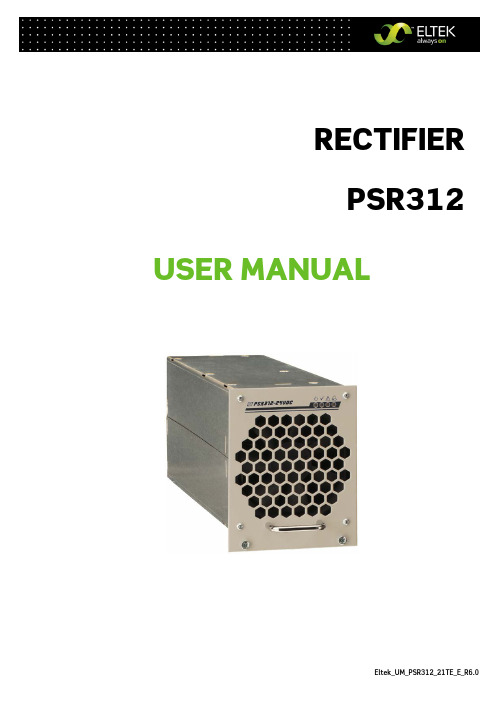
RECTIFIERPSR312 USER MANUALUser ManualPage 2 (20)Notes to this manualATTENTION! Read this manual very carefully before installing and commissioning the specified module. This manual is a part of the delivered module. Familiarity with the contents of this manual is required for installing and operating the specified module.The rules for prevention of accidents for the specific country and the general safety rules in accordance with IEC 364 must be observed.The function description in this manual corresponds to the date of publishing.Technical changes and changes in form and content can be made at any time by the manufacturer without notice. There are no obligations to update the manual continually.The module is manufactured in accordance with applicable DIN and VDE standards such as VDE 0106 (part 100) and VDE 0100 (part 410). The CE marking on the module confirms compliance with EU standards 2006-95-EG (low voltage) and 2004-108-EG (electromagnetic compatibility) if the installation and operation instructions are followed.Supplier:ELTEK DEUTSCHLAND GmbHBU IndustrialSchillerstraße 16D-32052 Herford☎+ 49 (0) 5221 1708-210FAX + 49 (0) 5221 1708-222Email *************************Internet Please note: No part of this document may be reproduced or transmitted in any form or by any means -electronic or mechanical, including photocopying and recording- for whatever reason without the explicit written permission of Eltek Deutschland GmbH.Changes and errors excepted.2011. ELTEK DEUTSCHLAND GmbH. All rights reserved.The current revision status of this user manual is the following:Revision: 6.0Date: 2010-11-23Writer Date00 First edition RTH 2008-01-0301 Minor text modifications, sections “Commissioning”, “Outputpower diagram” and “Monitoring” reworked, index of figuresinserted.RTH 2008-05-151.2 Minor text modifications, new revision status numberingintroduced. RTH 2008-11-042.0 Section 4.2.1 “Start-up behaviour” inserted; Technicalspecifications: Adjustable output voltage range changed.RTH 2009-04-29 3.0 Section 4.5 “Monitoring” reworked. RTH 2009-05-154.0 Minor text modifications, section 4.7 “Default value setting forNiCd batteries” inserted. RTH 2009-07-105.0 Technical specifications: “Internal decoupling circuit” corrected. RTH 2009-07-246.0 Input frequency range updated. RTH 2010-11-23Contents1A. Safety Instructions (5)1B. Electric Waste Disposal (5)2. General Information (6)3. Main Data/Equipment (6)3.1 Available Options and Assembly Equipment: (7)3.2 Front view/Front side LED panel (8)3.3 Rear Side Connection (9)3.4 Cooling and Air Flow Direction (10)3.5 Communication Interface (10)4. Handling (11)4.1 Storage (11)4.2 Commissioning (11)4.2.1 Start-up behaviour (11)4.3 Charge Characteristic/Output Power Diagram (12)4.4 LED Indications (13)4.5 Internal Monitoring (13)4.6 Threshold & Default Values (14)4.7 Default value setting for NiCd batteries (14)5. External Functions (15)6. Maintenance (15)7. Trouble Shooting (16)8. Technical Specifications (17)8.1 Dimensional Drawings: (19)Index of FiguresFigure 1) - DC Power Rack DCR PSR327-3.6 LV (7)Figure 2) - DC Power Rack DCR PSR327-4.8 LV (7)Figure 3) - Front view (8)Figure 4) - Male connectors (9)Figure 5) - Module air flow (10)Figure 6) - PSR312/24-50 Output Power Diagram (12)Figure 7) - Screenshot “PC software for CAN dongle” (14)Figure 8) - Module dimensions (19)1A. Safety InstructionsWarning!B ecause several components of operating electrical modules are charged by dangerous voltage, the improper handling of electrical modules may be the cause of accidents involving electrocution, injury, or material damages.•Operation and maintenance of electrical modules must be performed by qualified skilled personnel such as electricians in accordance with EN 50110-1 or IEC 60950.•Install the module only in areas with limited access to unskilled personnel.•B efore starting work, the electrical module must be disconnected from mains. Make sure that the module is earthed.•Do not touch connector pins as they can be charged with dangerous voltage up to 30 seconds after disconnection.•Only spare parts approved by the manufacturer must be used.1B. Electric Waste DisposalSeparate collection is the precondition to ensure specific treatment and recycling of waste electrical and electronic equipment and is necessary to achieve the chosen level of protection of human health and the environment.In the case of waste disposal of your discarded equipment we recommend to contact a waste management company.2. General InformationThe PSR312 rectifier rectifies sinusoidal AC input voltage to DC output voltage.The PSR312 is a hot plug-in module with rear side connectors and is designed to be mounted in an assembly set 19’’ sub rack (see section 3.1). Due to the state-of-the-art circuitry design, the unit has very low losses and therefore very compact dimensions, low weight and high power density.The PSR312 rectifier can be used in all DC applications with or without battery.The rectifier is delivered with factory set default values for lead acid batteries. If the rectifier is to be used for NiCd batteries, the default values must be parameterized accordingly using a CAN dongle and special software.The nominal output power per unit is 1.2 kW. Up to a maximum of 48 modules can be switched in parallel to increase the system output power or to build redundant power supply systems (n + 1-principle).3. Main Data/EquipmentNominal Output Current PSR312/24-50 101-012-148.00 24 V DC50 A DCNominal input voltage: 230 V ACNominal input current: 5.8 A ACInput frequency range: 16⅔ to 60 Hz (+5 %)Nominal output power: 1.2 kWFor more specific data, see section 8 please.3.1 Available Options and Assembly Equipment:DC Power Rack DCR PSR327-3.6 LV (assembly set 19’’ sub rack 3Uincl. backplane for three PSR312/24 V rectifiers and oneUPC3-24 V DC controller), DCC-CB1 connection board included. 102-327-318.LV01DC Power Rack DCR PSR327-4.8 LV (assembly set 19’’ sub rack 3U incl. backplane for four PSR312/24 V rectifiers). 102-327-408.LV01 Cover plate (with handle) to cover empty PSR slots, 1/4 x 19’’, 3U; RAL 7035881-MEC-BPL.03.21.B Monitoring, control and signalling unit (DC controller) UPC-24 V 301-003-498.02 DCC-CB1; connection board (with MSTB screw terminals) necessary to connect all measuring, control and signalling wires over the backplane of the sub rack to the control unit UPC3 (spare part) 302-DCC-CB1.00CAN dongle, incl. software; necessary to change the internal default values of the rectifier (e.g. for NiCd application).880-CAN-DNG.00Figure 1) - DC Power Rack DCR PSR327-3.6 LV fully equipped with three PSR312 rectifiers and one UPC3 DC controller Figure 2) - DC Power Rack DCR PSR327-4.8 LV fully equipped with four PSR312 rectifiers3.2Front view/Front side LED panelFigure 3) - Front view The PSR312 rectifier is equipped with the following four LED indicators:INPUT OKOUTPUT OKVout>ALARMFor more information about the LED indicators, see section 4.4Two captive screws are used for each module to secure it to the sub rack (components of the module)3.3 Rear Side ConnectionThe rear side male connections (AC input voltage, DC output voltage and signals) are shown in figure 4) and are defined in the table below.Figure 4) - Male connectors(shown from the rear side of the module)Pin assignment of the rear side connector:Pin Function2b L1 - Input5b N - Input8b - - -11b PE13a CAN - CVSS13c (-) output voltage sense link14a CAN - H14c CAN - L15a - - -15c CAN - CVCC16a AGND16c - - -17a Hardwarecoding CODE217c Hardwarecoding CODE118a Collective Alarm NC18c Collective Alarm COM19a Collective Alarm NO19c - - -20a - - -20c (+) output voltage sense link22b (-) Output25b (-) Output28b (+) Output31b (+) Output3.4 Cooling and Air Flow DirectionThe unit is cooled with an internal fan. The airflow is from the front to rear side. The fan is monitored and speed-controlled dependent on module temperature. To provide sufficient air flow, a minimum space (see item “A” in figure 5) of 50 mm is required between the unit and the rear cabinet wall as well as an unobstructed supply of air to the front of the module.Figure 5) - Module air flow3.5 Communication InterfaceThe PSR312 rectifier is equipped with a serial data interface in accordance with the Controller Area Network (CAN) specification. The CAN-Bus connection is integrated in the rear side connector.Several modules in a system or parallel connection can be controlled and monitored through the CAN-Bus by a central UPC DC controller unit.The following parameters of a specific rectifier unit can be controlled or monitored:•Output voltage•Output current•Module temperature•Module statusFurthermore, the rectifier unit receives all threshold values through the CAN-Bus from theDC controller unit.4. Handling4.1 StorageModules must be stored in a dry, dust free environment with a storage temperature in accordance with the specific technical data (see section 8).4.2 CommissioningNote:Before commissioning the module, make sure that the input voltage corresponds to the input voltage range of the unit as specified on the type plate and that the output voltage of paralleled units matches.1.Carefully unpack the unit2.Fill the rack beginning with the left slot.3.Put the unit into an empty slot.4.Carefully slide in the unit until the module connector touched the backplane connector.5.Increase the force until the unit fits in completely. Avoid using too much force. If the unit does notfit in, begin again at step 3.6.Secure the module using the two captive screws (M3x12) provided with the module.7.Switch ON the module by external MCB.Note: The PSR312 is serially equipped with an internal output side decoupling diode. This ensureshot plug-in capability for the module and enables the operator to add modules under operating conditions.Note: Before the module is to be removed it must be switched off by the external input fuse!Caution: After switching off the module the internal capacitors are still fully charged. Do not touch connector pins as they can still be charged with dangerous voltage after disconnection.4.2.1 Start-up behaviourWhen the PSR312 is switched on (without CAN-B us connection) first it provides a start-up voltage according to the table below. The start-up voltage is held for 60 seconds, than the output voltage steps up to the internal default value.Start-up voltage (V DC) 24.00Default value Vo (V DC) 27.25If a DC controller unit (UPC) is integrated into the system, it is powered with the start-up voltage after the rectifier has been switched on. The output voltage immediately steps up to the value given from the UPC unit via CAN-Bus.If a DC controller unit (UPC) is integrated into the system (e.g. powered by the battery and due to this operating yet) the rectifier directly provides the output voltage given from the UPC unit via CAN-Bus.4.3 Charge Characteristic/Output Power DiagramThe charge characteristic of the PSR312 is a power limited IV characteristic curve in accordance with DIN 41772/DIN 41773.For modules in parallel operation mode a load sharing of about ±10 % is attained due to a sloping output voltage line (-1 % at 100 % Inom).The module is continuous short circuit proof.Figure 6) - PSR312/24-50 Output Power DiagramCalculation of the output current (Io) at different output voltage values:The PSR312 rectifier provides an output power of Vonom x Ionom= Ponom (24 V x 50 A=1200 W)As shown with the output power diagram (see figure 6), the nominal output current (50 A) is available at nominal output voltage (24.0 V).At other output voltage values (e.g. float and boost charge voltage as well), the output current is corresponding to the following formula: Io= Ponom : VoExample 1):Float charge voltage for lead acid batteries (12 cells)= 27.24 V; Io= 1200 W : 27.24 V= 44 AExample 2):Boost charge voltage for lead acid batteries (12 cells)= 28.8 V; Io= 1200 W : 28.8 V= 41.7 A4.4 LED IndicationsFunctions of front panel LED indicators:For factory set**The module is equipped with an isolated signalling contact (normally open contact).The maximum load is 60 V DC/500 mA. The contact is time-delayed and reacts after approx. 10 sec.4.5 Internal MonitoringMonitored values Criteria FunctionAC input voltage I.) Mains input voltage 164 V≤ Vn≤ 195V Linearly decreases output power. II.) Mains input voltage <164 V Module automatically switches off. III.) Mains input voltage >184 V Module switches on.IV.) Mains input voltage >275 V Module switches off (self-locking). Itmust be manually restarted.DC output voltage Output voltage higher than theadjusted operating threshold*Module automatically switches off (selflocking). The unit must be manuallyrestarted.Moduletemperature Heat sink temperature ≥80 °C Module automatically switches off. It automatically switches on when the heat sink cools down to ≤70 °C.Cooling fan Cooling fan malfunction Module automatically switches off. After 30 sec. the module automatically tries three times to restart. If this fails, the module switches off and must be manually restarted.Short circuit Module automatically detects shortcircuit operation by the output voltagevalue. (criteria: Vout ≤83 % of Vnom)Module automatically switches off after3 seconds. After 30 seconds themodule automatically tries to restartrepeatedly.*For factory set output voltage threshold values, see section 4.64.6 Threshold & Default ValuesThe following table shows the factory set threshold/default values internally stored in the PSR312 unit (for lead acid battery):Output voltage Vo (V DC) 27.24Over voltage V> (V DC) 30.00Current limiting Iconst (A DC) 50.00Note: The threshold/default values can only be changed in combination with an UPC DC controller unit. If an UPC DC controller unit is controlling the power supply unit through the CAN-Bus, the charge voltage is completely controlled by the UPC based on its configuration values and momentary charge state (for example temperature compensation, boost charge, or battery test). That means that the values sentfrom the UPC over CAN-B us have top priority. During CAN-B us communication the internally stored values of the rectifier are invalid.B ut when the CAN-B us connection is inactive for more than five seconds (e. g. due to trouble), the PSR312 automatically switches back to the internally stored default values. In this case it is ensured that the battery is charged in the float charge mode.4.7 Default value setting for NiCd batteriesIf the rectifier is to be used to charge NiCd batteries the default/threshold values must be set according to the individual battery type using a CAN dongle and PC software (see section 3.2 “Available Options and Assembly Equipment”). A specific manual is available on request. For the adjusting range of the output voltage please see section 8 “Technical Specifications”.Figure 7) - Screenshot “PC software for CAN dongle”5. External FunctionsIf the rectifier works together with an UPC DC controller unit, the following external functions can be used:•Compensation of output voltage•Temperature compensation of charge voltage•Discharge test•Boost charge modeFor more information about these functions, read the UPC user manual.6. MaintenanceIn general, the rectifier is maintenance-free. Exclusively the fan is a component consisting of moving parts. By way of precaution a yearly inspection with following checks is recommended: •Mechanical/visual inspection•Removal of dust and dirt, especially on radiator surfaces•Check for internal dust or humidityIt is recommended to exchange the fan every five years.Attention!Dust combined with moisture or water may influence or destroy the internal electronic circuits.Dust inside the unit can be blown out with dry compressed air.The interval between the checks depends on ambient conditions of the installed module.7. Trouble ShootingNo output voltage Is mains voltage present? Check→Mains switched to “ON” position? CheckPSR312 module plugged in securely? CheckIncorrect polarity or short circuit at the output? CheckLED V> on? 1.) Switch the module off and on.2.) Check the settings forV> (see section 4.6).Deviation of the output voltage Is the unit operating in current limiting modedue to overload?Reduce the loadIs the output voltage setting Vout at the DCcontroller incorrect?Adjust output voltage to nominalvalues (see section 4.6)If an external sensor lead is used for the outputvoltage, is the connection faultless?CheckIf the unit still does not work even though all checks have been done, contact your sales agent or the service department of ELTEK DEUTSCHLAND GmbH.8. Technical SpecificationsArticle code 101-012-148.00AC input:Nominal input voltage 230 V AC ±20 %Nominal input current 5.8 A ACInput frequency range 16⅔ - 60 Hz (+5 %)Power factor >0.99 @ P >50 %Total harmonic distortion <5 %Efficiency ≥88 %Internal input fuse 16 A (6.3 x 32 mm)DC output:Nominal output voltage 24 V DCNominal output current 50 A DC @ 24 VNominal output power 1200 WCharge characteristic line IV characteristic according to DIN41772/DIN41773; power limited Output voltage threshold V>(factory setting)30 V DCAdjustable output voltage range 21 - 33 V DCDefault value of the chargingvoltage (factory set, 2.27 V/cell;lead acid battery*)27.24 V DCOutput over voltage Vo> (factoryset, 2.5 V/cell; lead acid battery*)30 V DCOutput under voltage Vo<(factory set, 1.7 V/cell; lead acidbattery*)20.4 V DC*Default/threshold values for charging of NiCd batteries are settable using a CAN dongle and PC software.Voltage ripple / psophometric acc. to CCITT-A ≤20 mVpp/ ≤ 1.2 mVDynamic accuracy of the charge voltage <3 % Vnom at load changes between 10 % - 90 % - 10 % Inom; transient time ≤1.5 msShort circuit protection continuous short circuit proof; 1x InomParallel operation Yes (max. 48 units with DC controller unit UPC); current sharing ≤10 % Inom;sloping output voltage line (-1 % at 100 % Inom)Internal active low-lossYes, in the negative output linedecoupling circuitInternal output fuse 80 AStandard Features:LED signalling Input OK (green), Vo OK (green), Vo> (red), Alarm (red)Main processor 16Bit FujitsuIsolated signalling contact “Collective alarm”; relay COM/NO/NC, maximum contact load: 60 V DC/500 mA Communications interface CAN-Bus, proprietary protocolEnvironmental:Ambient temperature Operation: -20 °C to +55 °C, storage: -40 °C to +85 °CClimatic conditions according to IEC 721-3-3 class 3K3/3Z1/3B1/3C2/3S2/3M2Max. installation altitude ≤1500 mAudible noise <45 dB (A)Mechanical:Type of construction ¼ x 19’’, 3UCooling Fan cooling (temperature-controlled, r.p.m.-monitored)Connector AC input, DC output and signals: DIN41612-M-connectorDimensions (W/H/D) 106.3/133/326.5 mmMinimum installation depth 438 mm (in combination with an assembly set 19’’ sub rack)Weight approx. 3.9 kgIP20 (front panel)/1Type of enclosure / ProtectionclassColour Front panel: RAL 7035, neutral, black print RAL 9005Compliances:CE conformity yesCompliance to safety standards EN60950-1; VDE0100 T410; VDE0110; EN50178; EN60146Compliance to EMC standards EN55022/24 (ITE), class “A“; EN61000-4 T2-58.1 Dimensional Drawings:Figure 8) - Module dimensionsSupplier:ELTEK DEUTSCHLAND GmbHBU IndustrialSchillerstraße 16D-32052 Herford☎+ 49 (0) 5221 1708-210FAX + 49 (0) 5221 1708-222Email *************************Internet 2011. ELTEK DEUTSCHLAND GmbH. All rights reserved.。
安捷伦(Agilent)P3211 pH复合电极说明书
P3211 pH combination electrode, Part Number 5190-3988*************(24小时)化学品安全技术说明书GHS product identifier 应急咨询电话(带值班时间)::供应商/ 制造商:安捷伦科技贸易(上海)有限公司中国(上海)外高桥自由贸易试验区英伦路412号(邮编:200131)电话号码: 800-820-3278传真号码: 0086 (21) 5048 2818P3211 pH combination electrode, Part Number 5190-3988化学品的推荐用途和限制用途* P3211 electrode P3211Reference solution 5190-0545-1部件号:物质用途:电极。
(1 x 7 ml(毫升))Reference solution1 x 30 ml部件号(化学品试剂盒):5190-3988注解 *:* 本产品被视为一件物品。
该安全数据表是针对本物品中的密封物质或混合物而编写。
在合理且符合使用说明的情况下使用本物品,不会存在健康风险。
该物品中的物质或混合物已密封。
仅在未按产品说明书使用或处理物品时,可能会存在潜在健康风险和安全隐患。
安全技术说明书根据 GB/ T 16483-2008 和 GB/ T 17519-2013GHS化学品标识:P3211 pH 复合电极,部件号 5190-3988危险性类别物质或混合物的分类根据 GB13690-2009 和 GB30000-2013皮肤腐蚀/刺激 - 类别 3H319严重眼损伤/眼刺激 - 类别 2AH371特异性靶器官毒性 一次接触 - 类别 2H400危害水生环境一急性危险 - 类别 1H410危害水生环境一长期危险 - 类别 1Reference solution H320严重眼损伤/眼刺激 - 类别 2B H400危害水生环境一急性危险 - 类别 1H410危害水生环境一长期危险 - 类别 1紧急情况概述* P3211 electrode 液体。
- 1、下载文档前请自行甄别文档内容的完整性,平台不提供额外的编辑、内容补充、找答案等附加服务。
- 2、"仅部分预览"的文档,不可在线预览部分如存在完整性等问题,可反馈申请退款(可完整预览的文档不适用该条件!)。
- 3、如文档侵犯您的权益,请联系客服反馈,我们会尽快为您处理(人工客服工作时间:9:00-18:30)。
Unit
typ
max
(--)1
µA
(--)1
µA
560
(390)380
MHz
(24)13
pF
Continued on next page.
Any and all SANYO products described or contained herein do not have specifications that can handle applications that require extremely high levels of reliability, such as life-support systems, aircraft's control systems, or other applications whose failure can be reasonably expected to result in serious physical and/or material damage. Consult with your SANYO representative nearest you before using any SANYO products described or contained herein in such applications.
Ordering number : ENN7221A
CPH3123 / CPH3223
PNP / NPN Epitaxial Planar Silicon Transistors
CPH3123 / CPH3223 High-Current Switching
Applications
Applications
3 --0.01
100
7
23
5 7 --0.1 2 3 5 7 --1.0
Collector Current, IC -- A
Cob -- VCB
23 5 IT04570
CPH3123 f=1MHz
5
3
Gain-Bandwidth Product, f T -- MHz
100
7 0.01
1000 7 5
Symbol
ICBO IEBO hFE
fT Cob
Conditions
VCB=(--)40V, IE=0 VEB=(--)4V, IC=0 VCE=(--)2V, IC=(--)100mA VCE=(--)10V, IC=(--)500mA VCB=(--)10V, f=1MHz
min 200
Ratings
+ 470µF
VCC=25V
Collector Current, IC -- A
--2.0
CPH3123
--1.8 --1.6 --1.4 --1.2
IC -- VCE
--40mA --30mA
--20mA
--1--08mmAA --6mA
--1.0
--4mA
--0.8
--0.6
--2mA
--0.4
• DC-DC converter, relay drivers, lamp drivers, motor drivers, flash.
Features
• Adoption of MBIT processes. • High current capacitance. • Low collector-to-emitter saturation voltage. • High-speed switching. • Ultrasmall package facilitates miniaturization in end products (mounting height : 0.9mm). • High allowable power dissipation.
CPH3123 / CPH3223
Continued from preceding page.
Parameter
Collector-to-Emitter Saturation Voltage
Base-to-Emitter Saturation Voltage Collector-to-Base Breakdown Voltage Collector-to-Emitter Breakdown Voltage Collector-to-Emitter Breakdown Voltage Emitter-to-Base Breakdown Voltage Turn-ON Time Storage Time Fall Time
Symbol
Conditions
VCE(sat)
VBE(sat) V(BR)CBO V(BR)CES V(BR)CEO V(BR)EBO
ton tstg
tf
IC=(--)1A, IB=(--)50mA IC=(--)2A, IB=(--)100mA IC=(--)2A, IB=(--)100mA IC=(--)10µA, IE=0 IC=(--)100µA, RBE=0 IC=(--)1mA, RBE=∞ IE=(--)10µA, IC=0 See specified Test Circuit.
SANYO assumes no responsibility for equipment failures that result from using products at values that exceed, even momentarily, rated values (such as maximum ratings, operating condition ranges, or other parameters) listed in products specifications of any and all SANYO products described or contained herein.
See specified Test Circuit.
See specified Test Circuit.
Ratings
Unit
min
typ
max
(--115)90 (--230)130 mV
(--240)160 (--650)240 mV
(--)0.88 (--)1.2
V
(--50)100
V
(--50)100
IC -- VBE3.0源自CPH3223VCE=2V
2.5
Collector Current, IC -- A
Collector Current, IC -- A Ta=75°C
25°C --25°C
--2.0
2.0
--1.5
1.5
--1.0
1.0
Ta=75°C 25°C
--25°C
--0.5
0 0
--0.2
Specifications ( ) : CPH3123
Absolute Maximum Ratings at Ta=25°C
Parameter Collector-to-Base Voltage Collector-to-Emitter Voltage Collector-to-Emitter Voltage Emitter-to-Base Voltage Collector Current Collector Current (Pulse) Base Current Collector Dissipation Junction Temperature Storage Temperature
CPH3123 / CPH3223
hFE -- IC
hFE -- IC
1000
1000
CPH3123
CPH3223
7
VCE= --2V
7
VCE=2V
5
Ta=75°C
25°C
3
--25°C
2
5
Ta=75°C
25°C
3
--25°C
2
DC Current Gain, hFE
DC Current Gain, hFE
V
(--)50
V
(--)6
V
(30)35
ns
(230)300
ns
(18)25
ns
Package Dimensions unit : mm 2150A
2.9 0.4
3
0.15 0.05
0.2
0.6 1.6 0.6 2.8
1
2
1.9
0.7 0.2 0.9
1 : Base 2 : Emitter 3 : Collector
10 --1.0
5 3 2
23
5 7 --10
23
5 7 --100
V
(--50)100
V
(--)50
V
(--)6
V
(--)3
A
(--)6
A
(--)600
mA
0.9
W
150
°C
--55 to +150
°C
Parameter
Collector Cutoff Current Emitter Cutoff Current DC Current Gain Gain-Bandwidth Product Output Capacitance Marking : CPH3123 : AU, CPH3223 : CU
--0.2 0 0
--3.0
--2.5
IB=0
--0.1 --0.2 --0.3 --0.4 --0.5 --0.6 --0.7 --0.8 --0.9 --1.0
