JAN2N6249中文资料
JANTX2N3634中文资料
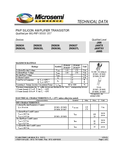
2N3634* 2N3635*
140 140
2N3636* 2N3637*
175 175
Unit
TO-39* (TO-205AD) 2N3634, 2N3635 2N3636, 2N3637
Vdc Vdc 5.0 Vdc 1.0 Adc @ TA = +250C(1) 1.0 W PT @ TC = +250C(2) 5.0 W 0 Operating & Storage Junction Temperature Range -65 to +200 C TJ, Tstg *Electrical characteristics for “L” suffix devices are identical to the “non L” corresponding devices 1) Derate linearly 5.71 mW/0C for TA > +250C 2) Derate linearly 28.6 mW/0C for TC > +250C
f = 100 Hz f = 1.0 kHz f = 10 kHz
NF
dB
SAFE OPERATING AREA
DC Tests TC = 250C, 1 Cycle, t = 1.0 s Test 1 VCE = 100 Vdc, IC = 30 mAdc 2N3634, 2N3635 VCE = 130 Vdc, IC = 20 mAdc 2N3636, 2N3637 Test 2 VCE = 50 Vdc, IC = 95 mAdc Test 3 VCE = 5.0 Vdc, IC = 1.0 Adc (3) Pulse Test: Pulse Width = 300µs, Duty Cycle ≤ 2.0%.
JANTXV2N6788U中文资料

TJ TSTG
Operating Junction Storage Temperature Range Pckg. Mounting Surface Temp.
Weight
For footnotes refer to the last page
LCC-18
Features:
n Surface Mount n Small Footprint n Alternative to TO-39 Package n Hermetically Sealed n Dynamic dv/dt Rating n Avalanche Energy Rating n Simple Drive Requirements n Light Weight
Note: Corresponding Spice and Saber models are available on International Rectifier Website. For footnotes refer to the last page
2
元器件交易网
15V
VDS
L
DRIVER
RG
2V0GVS tp
D.U.T IAS
0.01Ω
+ - VDD
A
Fig 12a. Unclamped Inductive Test Circuit
V(BR)DSS tp
Fig 12c. Maximum Avalanche Energy Vs. Drain Current
IAS
Thermal Resistance
Parameter
RthJC RthJ-PCB
Junction to Case Junction to PC Board
JANSR2N7382中文资料
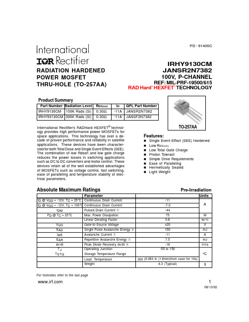
TO-257AA
Features:
n Single Event Effect (SEE) Hardened n Low RDS(on) n Low Total Gate Charge n Proton Tolerant n Simple Drive Requirements n Ease of Paralleling n Hermetically Sealed n Light Weight
300 (0.063 in (1.6mm)from case for 10s)
4.3 (Typical)
g
For footnotes refer to the last page
1
06/13/02
元器件交易网
IRHY9130CM, JANSR2N7382
— 70
6.8 —
nH Measured from drain lead (6mm/0.25in. from
package) to source lead (6mm/0.25in. from
package)
Ciss Coss Crss
Input Capacitance Output Capacitance Reverse Transfer Capacitance
Pre-Irradiation
Electrical Characteristics @ Tj = 25°C (Unless Otherwise Specified)
Parameter
Min
BVDSS
Drain-to-Source Breakdown Voltage -100
∆BVDSS/∆TJ Temperature Coefficient of Breakdown — Voltage
JANSF2N7422U资料

(REF:MIL-PRF-19500/662) P-CHANNEL
RAD HARD
Product Summary
International Rectifier’s P-Channel RAD HARD technology Part Number BVDSS
RDS(on)
ID
HEXFETs demonstrate excellent threshold voltage stability
as voltage control, very fast switching, ease of paralleling n Lightweight
and temperature stability of the electrical parameters. They
are well-suited for applications such as switching power sup-
RDS(on)
Static Drain-to-Source On-State Resistance
Voltage Forward Transconductance Zero Gate Voltage Drain Current
IGSS IGSS Qg Qgs Qgd td(on) tr td(off) tf LD
— — -22 — — -88
A Modified MOSFET symbol showingtheintegral
reverse p-n junction rectifier.
VSD trr QRR
ton
Diode Forward Voltage Reverse Recovery Time Reverse Recovery Charge
2N5116JAN中文资料

2N5114JAN/JANTX/JANTXV SeriesVishay SiliconixDocument Number: 70261S-04030—Rev . E, 04-Jun-019-1P-Channel JFETs2N5114JAN/JANTX/JANTXV 2N5115JAN/JANTX/JANTXV 2N5116JAN/JANTX/JANTXVFEATURESBENEFITSAPPLICATIONSD Low On-Resistance: 2N5114 <75 W D Fast Switching—t ON : 16 nsD High Off-Isolation—I D(off): –10 pA D Low Capacitance: 6 pF DLow Insertion LossD Low Error VoltageD High-Speed Analog Circuit Performance D Negligible “Off-Error,” Excellent Accuracy D Good Frequency Response DEliminates Additional BufferingD Analog Switches D ChoppersD Sample-and-HoldD Normally “On” Switches DCurrent LimitersDESCRIPTIONThe 2N5114JAN/JANTX/JANTXV series consists of p-channel JFET analog switches designed to provide low on-resistance, good off-isolation, and fast switching. TheseJFETs are optimized for use in complementary switching applications with the Vishay Siliconix 2N4856A series.TO-206AA (TO-18)ABSOLUTE MAXIMUM RATINGSGate-Drain Voltage 30 V . . . . . . . . . . . . . . . . . . . . . . . . . . . . . . . . . . . . . . . . . . . . . Gate-Source Voltage 30 V . . . . . . . . . . . . . . . . . . . . . . . . . . . . . . . . . . . . . . . . . . . . Gate Current –50 mA . . . . . . . . . . . . . . . . . . . . . . . . . . . . . . . . . . . . . . . . . . . . . . . . Storage Temperature –65 to 200_C . . . . . . . . . . . . . . . . . . . . . . . . . . . . . . . . . . . Operating Junction Temperature –55 to 200_C . . . . . . . . . . . . . . . . . . . . . . . . . . Lead Temperature (1/16” from case for 10 sec.)300_C. . . . . . . . . . . . . . . . . . . Power Dissipation a 500 mW . . . . . . . . . . . . . . . . . . . . . . . . . . . . . . . . . . . . . . . . . Notesa.Derate 3 mW/_C above 25_C2N5114JAN/JANTX/JANTXV Series Vishay Siliconix 9-2Document Number: 70261 S-04030—Rev. E, 04-Jun-01Notesa.Typical values are for DESIGN AID ONLY, not guaranteed nor subject to production testing.PSCIAb.Pulse test: PW v300 m s duty cycle v3%.c.This parameter not registered with JEDEC.2N5114JAN/JANTX/JANTXV SeriesVishay SiliconixDocument Number: 70261S-04030—Rev . E, 04-Jun-019-3*Non-inductiveINPUT PULSESAMPLING SCOPERise Time < 1 ns Fall Time < 1 ns Pulse Width 100 ns PRF 1 MHzRise Time 0.4 nsInput Resistance 10 M W Input Capacitance 1.5 pFSee Typical Characteristics curves for changes.WWV GG –V DD。
JAN4N48中文资料

4N474N48JAN, JANTX, JANTXV, SINGLE CHANNEL OPTOCOUPLERS 4N49Mii OPTOELECTRONIC PRODUCTS{PRIVATE }DIVISIONFeatures:• High Reliability• Base lead provided for conventional transistor biasing• Rugged package• High gain, high voltage transistor• +1kV electrical isolation Applications:• Eliminate ground loops • Level shifting• Line receiver• Switching power supplies • Motor controlDESCRIPTIONGallium Aluminum Arsenide (GaAlAs) infrared LED and a high gain N-P-N silicon phototransistor packaged in a hermetically sealed TO-5 metal can. The 4N47, 4N48 and 4N49’s can be tested to customer specifications, as well as to MIL-PRF-19500 JAN, JANTX, JANTXV and JANS quality levels.*ABSOLUTE MAXIMUM RATINGSInput to Output Voltage.............................................................................................................................................................1kV Emitter-Collector Voltage (7V)Collector-Emitter Voltage (Value applies to emitter-base open-circuited & the input-diode equal to zero) (40V)Collector-Base Voltage (45V)Reverse Input Voltage (2V)Input Diode Continuous Forward Current at (or below) 65°C Free-Air Temperature (see note 1)......................................40mA Peak Forward Input Current (Value applies for tw < 1µs, PRR < 300 pps)...............................................................................1A Continuous Collector Current................................................................................................................................................50mA 元器件交易网*ELECTRICAL CHARACTERISTICS T A = 25°C Unless otherwise specifiedPARAMETER SYMBOL MIN TYP MAX UNITS TEST CONDITIONS NOTEInput Diode Static Reverse Current I R 100 µA V R = 2V Input Diode Static Forward Voltage-55°C +25°C+100°CV F1.0 0.8 0.71.41.7 1.5 1.3VI E = 10mA*OUTPUT TRANSISTOR T A = 25°C Unless otherwise specifiedPARAMETER SYMBOL MIN TYP MAX UNITS TEST CONDITIONS NOTECollector-Base Breakdown VoltageV (BR)CBO 45VI C = 100µA, I B = 0, I F = 0 Collector-Emitter Breakdown Voltage V (BR)CEO 40 V I C = 1mA, I B = 0, I F = 0Emitter-Collector Breakdown VoltageV (BR)EBO7V I C = 0, I E = 100µA, I F = 0*COUPLED CHARACTERISTICS T A = 25°C Unless otherwise specified PARAMETER SYMBOL MIN TYP MAX UNITS TEST CONDITIONS NOTEOn State Collector Current 4N47 4N48 4N49 I C(ON) 0.5 1.0 2.05 10 mA V CE = 5V, I B = 0, I F = 1mAOn State Collector Current 4N47 -55°C 4N48 4N49 I C(ON)0.7 1.4 2.8 mAV CE = 5V, I B = 0, I F = 2mAOn State Collector Current 4N47 +100°C 4N484N49I C(ON)0.5 1.0 2.0mAV CE = 5V, I B = 0, I F = 2mA2 Off State Collector Current +25°C I C(OFF) 100 nA V CE = 20V, I B = 0, I F = 0mA Off State Collector Current +100°C I C(OFF) 100 µA V CE = 20V, I B = 0, I F = 0mA Collector-Emitter Saturation Voltage4N474N48 4N49 V CE(SAT) V CE(SAT) V CE(SAT)0.3 0.3 0.3VV V I C = 0.5mA, I B = 0, I F = 2mA I C = 1mA, I B = 0, I F = 2mA I C = 2mA, I B = 0, I F = 2mAInput to Output Resistance R I-O 1011V IN-OUT = 1kV 1 Input to Output CapacitanceC I-O5pFf = 1MHz, V IN-OUT = 1kV 1 Rise Time/ Fall Time 4N47 Phototransistor Operation 4N48 4N49 t r / t f t r / t f t r / t f 20 2525 µsµs µsV CC = 10V, I F = 10mA, R L = 100ΩRise Time/ Fall Time 4N47 Photodiode Operation 4N484N49t r / t f t r / t f t r / t f0.85 0.85 0.85µsµs µsV CC = 10V, I F = 10mA, R L = 100ΩNOTES:1. These parameters are measured between all phototransistor leads shorted together and with both input diode leads shorted together.2. This parameter measured using pulse techniques t w =100µs, duty cycle < 1%.RECOMMENDED OPERATING CONDITIONS:UNITSMAXMINPARAMETER SYMBOLInput Current, Low Level I FL0 100 µAInput Current, High Level I FH 2 10 mASupply Voltage V CE 5 10 VSELECTION GUIDEPART NUMBER PART DESCRIPTIONJAN4N47 4N47 Optocoupler, JAN Screening levelJAN4N48 4N48 Optocoupler, JAN Screening levelJAN4N49 4N49 Optocoupler, JAN Screening levelJANTX4N47 4N47Optocoupler, JANTX Screening levelOptocoupler, JANTX Screening levelJANTX4N48 4N48Optocoupler, JANTX Screening levelJANTX4N49 4N49JANTXV4N47 4N47 Optocoupler, JANTXV Screening levelJANTXV4N48 4N48 Optocoupler, JANTXV Screening levelJANTXV4N49 4N49 Optocoupler, JANTXV Screening levelJANS4N47 4N47 Optocoupler, JANS Screening levelJANS4N48 4N48 Optocoupler, JANS Screening levelJANS4N49 4N49 Optocoupler, JANS Screening level*JEDEC registered data。
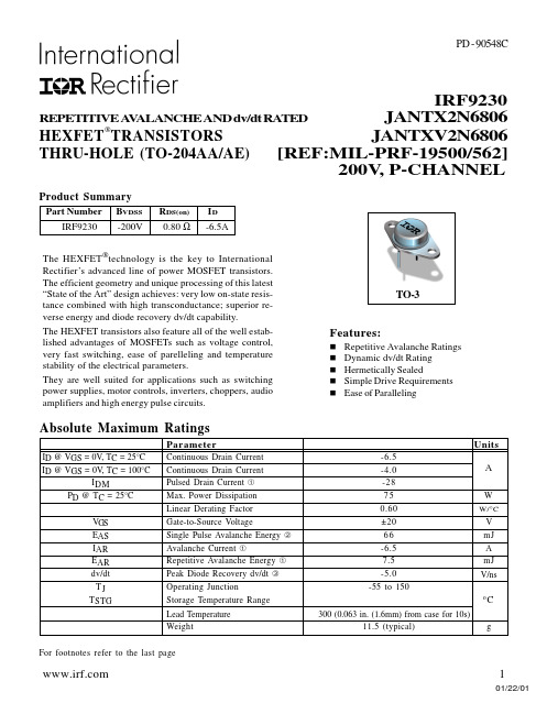
JANTXV2N6806中文资料
TJ TSTG
Operating Junction Storage Temperature Range Lead Temperature Weight
TO-3
Features:
n Repetitive Avalanche Ratings n Dynamic dv/dt Rating n Hermetically Sealed n Simple Drive Requirements n Ease of Paralleling
4
Fig 8. Maximum Safe Operating Area
元器件交易网
Fig 9. Maximum Drain Current Vs. Case Temperature
IRF9230
VDS VGS RG
RD D.U.T.
-10V
Pulse Width ≤ 1 µs Duty Factor ≤ 0.1 %
For footnotes refer to the last page
2
Min Typ Max Units
— — 1.67 °C/W — — 30
Test Conditions Soldered to a 2” square copper-clad board
元器件交易网
Units
-6.5
-4.0
A
-28
75
W
0.60
W/°C
±20
V
66
mJ
-6.5
A
7.5
mJ
-5.0
V/ns
-55 to 150 oC
300 (0.063 in. (1.6mm) from case for 10s)
JAN2N3821中文资料
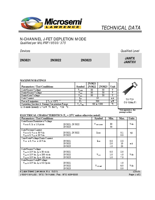
TECHNICAL DATA N-CHANNEL J-FET DEPLETION MODEQualified per MIL-PRF-19500/375Devices Qualified Level2N3821 2N3822 2N3823JANTX JANTXVMAXIMUM RATINGSParameters / Test Conditions Symbol 2N38212N3822 2N3823 UnitGate-Source Voltage V GSR50 30 V Drain-Source Voltage V DS50 30 V Drain-Gate Voltage V DG50 30 V Gate Current I GF 10 mA Power Dissipation T A = +250C (1)P T300 mW Operating Junction & Storage Temperature Range T j, T stg-55 to +200 0C(1) Derate linearly 1.7 mW/C for T A +25 C.package outline ELECTRICAL CHARACTERISTICS (T A = 250C unless otherwise noted)Parameters / Test Conditions Symbol Min. Max. Units Gate-Source Breakdown VoltageV DS = 0, I G = 1.0 µAdc 2N3821, 2N3822 2N3823 V(BR)GSSR5030VdcGate Reverse CurrentV DS = 0, V GS = 30 Vdc 2N3821, 2N3822 V DS = 0, V GS = 20 Vdc 2N3823 I GSSR0.10.5ηAZero-Gate-Voltage Drain CurrentV GS = 0, V DS = 15 Vdc 2N3821 2N3822 2N3823 I DSS0.52.04.02.51020mAGate-Source VoltageV DS = 15 Vdc, I D = 50 µAdc 2N3821V DS = 15 Vdc, I D = 200 µAdc 2N3822 V DS = 15 Vdc, I D = 400 µAdc 2N3823 V GS0.51.01.02.04.07.5VdcGate-Source Cutoff VoltageV DS = 15 Vdc, I D = 0.5 ηAdc 2N38212N3822 2N3823 V GS(off)4.06.08.0Vdc6 Lake Street, Lawrence, MA 018411-800-446-1158 / (978) 794-1666 / Fax: (978) 689-0803120101 Page 1 of 22N3821, 2N3822, 2N3823 JAN SERIESParameters / Test Conditions Symbol Min. Max. Units Small-Signal Common Source, Short-Circuit Forward Transfer AdmittanceV GS = 0, V DS = 15 Vdc, f = 1.0 kHz 2N38212N3822 2N3823 |y fs|1150030003500450065006500µSSmall-Signal Common Source, Short-Circuit Output AdmittanceV GS = 0, V DS = 15 Vdc, f = 1.0 kHz 2N38212N3822 2N3823 |y os|102035µSSmall-Signal, Common-Source Short-Circuit Input CapacitanceV GS = 0, V DS = 15 Vdc, 100 kHz ≤ f ≤ 1.0 MHz C iss 6.0 pF Small-Signal, Common-Source Reverse Transfer CapacitanceV DS = 15 Vdc, V GS = 0, 100 kHz ≤ f ≤ 1.0 MHz2N3821, 2N3822 2N3823C rss3.02.0pFSmall-Signal Common Source, Short-Circuit Forward Transfer AdmittanceV GS = 0, V DS = 15 Vdc, f = 100 MHz 2N3821f = 100 MHz 2N3822 f = 200 MHz 2N3823 |y fs|2150030003200µSSmall-Signal, Common-Source Short-Circuit Input ConductanceV GS = 0, V DS = 15 Vdc, f = 200 MHz 2N3823 (only)g is 800 µS Small-Signal, Common-Source Short-Circuit Output ConductanceV GS = 0, V DS = 15 Vdc, f = 200 MHz 2N3823 (only)g os 200 µS Common Source Spot Noise FigureV GS = 0, V DS = 15 Vdc, R G = 1MΩf = 10 Hz2N3821, 2N3822f = 1.0 kHz 2N3821, 2N3822, 2N3823NF1 5.02.0dBCommon Source Spot Noise FigureV GS = 0, V DS = 15 Vdc, R G = 1kΩf = 105 MHz2N3823 (only)NF22.5dB6 Lake Street, Lawrence, MA 018411-800-446-1158 / (978) 794-1666 / Fax: (978) 689-0803120101 Page 2 of 2。
JANSF2N7269中文资料

RthJC RthCS RthJA
Junction-to-Case Case-to-sink Junction-to-Ambient
Min Typ Max Units
— — 0.83 °C/W
— 0.21 — — — 48
Test Conditions Typical socket mount
Note: Corresponding Spice and Saber models are available on the International Rectifier Website. For footnotes refer to the last page
元器件交易网
PD - 90674D
RADIATION HARDENED POWER MOSFET THRU-HOLE (TO-254AA)
IRHM7250 JANSR2N7269
200V, N-CHANNEL
REF: MIL-PRF-19500/603 RAD-Hard™ HEXFET® TECHNOLOGY
Absolute Maximum Ratings
Pre-Irradiation
Parameter
Units
ID @ VGS = 12V, TC = 25°C ID @ VGS = 12V, TC = 100°C
IDM PD @ TC = 25°C
Continuous Drain Current Continuous Drain Current Pulsed Drain Current À Max. Power Dissipation Linear Derating Factor
VGS = 0V, TJ = 125°C
JANTXV2N6782U中文资料

VGS EAS IAR EAR dv/dt
Gate-to-Source Voltage Single Pulse Avalanche Energy ➁ Avalanche Current ➀ Repetitive Avalanche Energy ➀ Peak Diode Recovery dv/dt ➂
gfs
Forward Transconductance
0.8 — — S ( )
Ω
VDS > 15V, IDS =2.25A➃
IDSS
Zero Gate Voltage Drain Current
— — 25
—
— 250 µA
VDS=80V, VGS=0V VDS =80V
VGS = 0V, TJ = 125°C
100V, N-CHANNEL
Product Summary Part Number BVDSS IRFE110 100V
RDS(on) 0.60Ω
ID 3.5A
The leadless chip carrier (LCC) package represents the logical next step in the continual evolution of surface mount technology. Desinged to be a close replacement for the TO-39 package, the LCC will give designers the extra flexibility they need to increase circuit board density. International Rectifier has engineered the LCC package to meet the specific needs of the power market by increasing the size of the bottom source pad, thereby enhancing the thermal and electrical performance. The lid of the package is grounded to the source to reduce RF interference.
JANTX2N6806中文资料
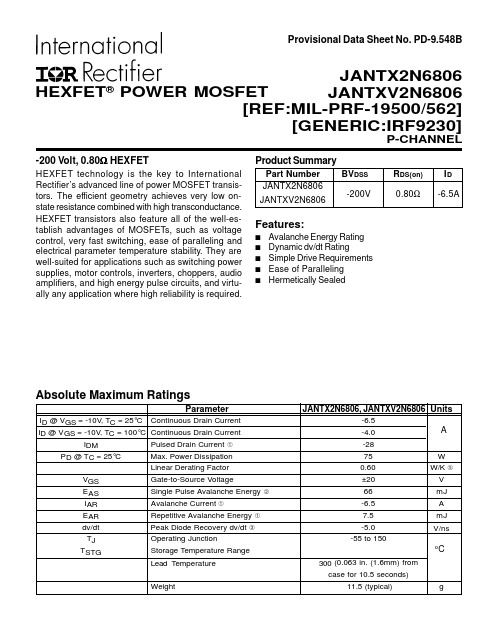
Product SummaryPart Number BV DSS R DS(on)I D JANTX2N6806JANTXV2N6806Features:s Avalanche Energy Rating s Dynamic dv/dt Ratings Simple Drive Requirements s Ease of Paralleling sHermetically SealedP-CHANNELProvisional Data Sheet No. PD-9.548B-200 Volt, 0.80Ω HEXFETHEXFET technology is the key to International Rectifier’s advanced line of power MOSFET transis-tors. The efficient geometry achieves very low on-state resistance combined with high transconductance.HEXFET transistors also feature all of the well-es-tablish advantages of MOSFETs, such as voltage control, very fast switching, ease of paralleling and electrical parameter temperature stability. They are well-suited for applications such as switching power supplies, motor controls, inverters, choppers, audio amplifiers, and high energy pulse circuits, and virtu-ally any application where high reliability is required.JANTX2N6806JANTXV2N6806[REF:MIL-PRF-19500/562][GENERIC:IRF9230]HEXFET ® POWER MOSFET Absolute Maximum RatingsParameterJANTX2N6806, JANTXV2N6806UnitsI D @ V GS = -10V , T C = 25°C Continuous Drain Current -6.5 I D @ V GS = -10V , T C = 100°CContinuous Drain Current -4.0I DMPulsed Drain Current -28P D @ T C = 25°CMax. Power Dissipation 75W Linear Derating Factor 0.60W/K V GS Gate-to-Source Voltage±20V E AS Single Pulse Avalanche Energy 66mJ I AR Avalanche Current-6.5A E AR Repetitive Avalanche Energy 7.5mJ dv/dt Peak Diode Recovery dv/dt -5.0V/nsT J Operating Junction-55 to 150T STGStorage Temperature Range Lead Temperature 300(0.063 in. (1.6mm) from case for 10.5 seconds)Weight11.5 (typical)go CA-6.5A0.80Ω-200VThermal ResistanceParameterMin.Typ.Max.UnitsTest ConditionsR thJC Junction-to-Case —— 1.67R thJAJunction-to-Ambient——30K/WTypical socket mountSource-Drain Diode Ratings and CharacteristicsParameterMin.Typ.Max.UnitsTest ConditionsI S Continuous Source Current (Body Diode)——-6.5Modified MOSFET symbol showing the I SMPulse Source Current (Body Diode)——-28integral reverse p-n junction rectifier.V SD Diode Forward Voltage ——-6.0V T j = 25°C, I S = -6.5A, V GS = 0V t rr Reverse Recovery Time ——400ns T j = 25°C, I F = -6.5A, di/dt ≤ -100A/µsQ RR Reverse Recovery Charge —— 4.0µCV DD ≤ -50Vt onForward Turn-On TimeIntrinsic turn-on time is negligible. Turn-on speed is substantially controlled by L S + L D .Electrical Characteristics @ Tj = 25°C (Unless Otherwise Specified)DS = -25Vf = 1.0 MHz see figure 5AFig. 2 — T ypical Output CharacteristicsT C = 150°CFig. 3 — Typical Transfer Characteristics Fig. 4 — Normalized On-Resistance Vs.TemperatureFig. 5 — T ypical Capacitance Vs. Drain-to-SourceVoltage Fig. 6 — T ypical Gate Charge Vs. Gate-to-SourceVoltageFig. 10b — Switching Time WaveformsFig. 10a — Switching Time Test Circuit Fig. 8 — Maximum Safe Operating AreaFig. 9 — Maximum Drain Current Vs. Case TemperatureFig. 7 — Typical Source-to-Drain Diode ForwardVoltageFig. 12c — Max. Avalanche Energy vs. Current Fig. 13a — Gate Charge T est CircuitFig. 12a — Unclamped Inductive T est Circuit Fig. 12b — Unclamped Inductive WaveformsFig. 11 — Maximum Effective Transient Thermal Impedance, Junction-to-Case Vs. Pulse DurationCase Outline and Dimensions — TO-204AA (Modified TO-3)Repetitive Rating; Pulse width limited by maximum junction temperature.(see figure 11)@ V DD = -50V, Starting T J = 25°C,E AS = [0.5 * L * (I L 2) * [BV DSS /(BV DSS -V DD )]Peak I L = -6.5A, V GS = -10V , 25 ≤ R G ≤ 200Ω I SD ≤ -6.5A, di/dt ≤ -120A/µs,V DD ≤ BV DSS , T J ≤ 150°CPulse width ≤ 300 µs; Duty Cycle ≤ 2%K/W = °C/W W/K = W/°CWORLD HEADQUARTERS: 233 Kansas St., El Segundo, California 90245, Tel: (310) 322 3331EUROPEAN HEADQUARTERS: Hurst Green, Oxted, Surrey RH8 9BB, UK Tel: ++ 44 1883 732020IR CANADA: 7321 Victoria Park Ave., Suite 201, Markham, Ontario L3R 2Z8, Tel: (905) 475 1897IR GERMANY: Saalburgstrasse 157, 61350 Bad Homburg Tel: ++ 49 6172 96590IR ITALY: Via Liguria 49, 10071 Borgaro, Torino Tel: ++ 39 11 451 0111IR FAR EAST: K&H Bldg., 2F, 3-30-4 Nishi-Ikeburo 3-Chome, Toshima-Ki, Tokyo Japan 171 Tel: 81 3 3983 0086IR SOUTHEAST ASIA: 315 Outram Road, #10-02 Tan Boon Liat Building, Singapore 0316 Tel: 65 221 8371/Data and specifications subject to change without notice.10/96All dimensions are shown millimeters (inches)。
半导体型号命名规则

一、中国半导体器件型号命名方法半导体器件型号由五部分(场效应器件、半导体特殊器件、复合管、PIN型管、激光器件的型号命名只有第三、四、五部分)组成。
五个部分意义如下:第一部分:用数字表示半导体器件有效电极数目。
2-二极管、3-三极管第二部分:用汉语拼音字母表示半导体器件的材料和极性。
表示二极管时:A-N型锗材料、B-P 型锗材料、C-N型硅材料、D-P型硅材料。
表示三极管时:A-PNP型锗材料、B-NPN型锗材料、C-PNP 型硅材料、D-NPN型硅材料。
第三部分:用汉语拼音字母表示半导体器件的内型。
P-普通管、V-微波管、W-稳压管、C-参量管、Z-整流管、L-整流堆、S-隧道管、N-阻尼管、U-光电器件、K-开关管、X-低频小功率管(F<3MHz,Pc<1W)、G-高频小功率管(f>3MHz,Pc<1W)、D-低频大功率管(f<3MHz,Pc>1W)、A-高频大功率管(f>3MHz,Pc>1W)、T-半导体晶闸管(可控整流器)、Y-体效应器件、B-雪崩管、J-阶跃恢复管、CS-场效应管、BT-半导体特殊器件、FH-复合管、PIN-PIN型管、JG-激光器件。
第四部分:用数字表示序号第五部分:用汉语拼音字母表示规格号例如:3DG18表示NPN型硅材料高频三极管二、日本半导体分立器件型号命名方法日本生产的半导体分立器件,由五至七部分组成。
通常只用到前五个部分,其各部分的符号意义如下:第一部分:用数字表示器件有效电极数目或类型。
0-光电(即光敏)二极管三极管及上述器件的组合管、1-二极管、2三极或具有两个pn结的其他器件、3-具有四个有效电极或具有三个pn结的其他器件、┄┄依此类推。
第二部分:日本电子工业协会JEIA注册标志。
S-表示已在日本电子工业协会JEIA注册登记的半导体分立器件。
第三部分:用字母表示器件使用材料极性和类型。
A-PNP型高频管、B-PNP型低频管、C-NPN 型高频管、D-NPN型低频管、F-P控制极可控硅、G-N控制极可控硅、H-N基极单结晶体管、J-P沟道场效应管、K-N沟道场效应管、M-双向可控硅。
JANTXV2N6796中文资料
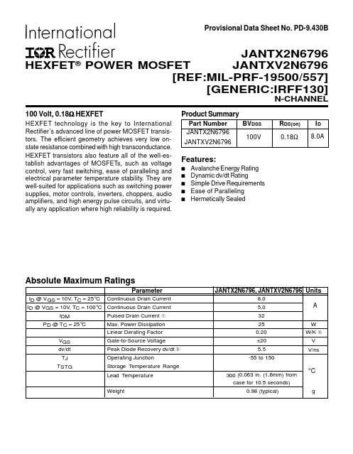
Product SummaryPart Number BV DSS R DS(on)I D JANTX2N6796JANTXV2N6796Features:s Avalanche Energy Rating s Dynamic dv/dt Ratings Simple Drive Requirements s Ease of Paralleling sHermetically SealedN-CHANNELProvisional Data Sheet No. PD-9.430B100 Volt, 0.18Ω HEXFETHEXFET technology is the key to International Rectifier’s advanced line of power MOSFET transis-tors. The efficient geometry achieves very low on-state resistance combined with high transconductance.HEXFET transistors also feature all of the well-es-tablish advantages of MOSFETs, such as voltage control, very fast switching, ease of paralleling and electrical parameter temperature stability. They are well-suited for applications such as switching power supplies, motor controls, inverters, choppers, audio amplifiers, and high energy pulse circuits, and virtu-ally any application where high reliability is required.JANTX2N6796JANTXV2N6796[REF:MIL-PRF-19500/557][GENERIC:IRFF130]HEXFET ® POWER MOSFET ParameterJANTX2N6796, JANTXV2N6796UnitsI D @ V GS = 10V, T C = 25°C Continuous Drain Current 8.0I D @ V GS = 10V , T C = 100°CContinuous Drain Current 5.0I DMPulsed Drain Current 32P D @ T C = 25°CMax. Power Dissipation 25W Linear Derating Factor 0.20W/K V GS Gate-to-Source Voltage±20V dv/dt Peak Diode Recovery dv/dt 5.5V/nsT J Operating Junction-55 to 150T STGStorage Temperature Range Lead Temperature 300(0.063 in. (1.6mm) from case for 10.5 seconds)Weight0.98 (typical)goCA8.0A0.18Ω100V元器件交易网Thermal ResistanceParameterMin.Typ.Max.UnitsTest ConditionsR thJC Junction-to-Case —— 5.0R thJAJunction-to-Ambient——175K/WTypical socket mountSource-Drain Diode Ratings and CharacteristicsParameterMin.Typ.Max.UnitsTest ConditionsI S Continuous Source Current (Body Diode)——8.0Modified MOSFET symbol showing the I SMPulse Source Current (Body Diode)——32integral reverse p-n junction rectifier.V SD Diode Forward Voltage —— 1.5V T j = 25°C, I S = 8.0A, V GS = 0V t rr Reverse Recovery Time ——300ns T j = 25°C, I F = 8.0A, di/dt ≤ 100A/µsQ RR Reverse Recovery Charge —— 3.0µCV DD ≤ 50Vt onForward Turn-On TimeIntrinsic turn-on time is negligible. Turn-on speed is substantially controlled by L S + L D .Electrical Characteristics @ Tj = 25°C (Unless Otherwise Specified)DS = 25Vf = 1.0 MHz see figure 5AFig. 1 — T ypical Output CharacteristicsT C = 25°C Fig. 2 — T ypical Output CharacteristicsT C = 150°CFig. 3 — Typical Transfer Characteristics Fig. 4 — Normalized On-Resistance Vs.TemperatureFig. 5 — T ypical Capacitance Vs. Drain-to-SourceVoltage Fig. 6 — T ypical Gate Charge Vs. Gate-to-SourceVoltageFig. 10b — Switching Time WaveformsFig. 10a — Switching Time Test Circuit Fig. 8 — Maximum Safe Operating AreaFig. 9 — Maximum Drain Current Vs. Case TemperatureFig. 7 — Typical Source-to-Drain Diode ForwardVoltageFig. 13a — Gate Charge T est CircuitFig. 12a — Unclamped Inductive T est Circuit Fig. 12b — Unclamped Inductive WaveformsFig. 11 — Maximum Effective Transient Thermal Impedance, Junction-to-Case Vs. Pulse DurationJANTX2N6796, JANTXV2N6796 DeviceCase Outline and Dimensions — TO-205AF (Modified TO-39)Repetitive Rating; Pulse width limited by maximum junction temperature.(see figure 11)@ V DD = 25V , Starting T J = 25°C,E AS = [0.5 * L * (I L 2) * [BV DSS /(BV DSS -V DD )]Peak I L = 8.0A, V GS = 10V , 25 ≤ R G ≤ 200ΩWORLD HEADQUARTERS: 233 Kansas St., El Segundo, California 90245, Tel: (310) 322 3331EUROPEAN HEADQUARTERS: Hurst Green, Oxted, Surrey RH8 9BB, UK Tel: ++ 44 1883 732020IR CANADA: 7321 Victoria Park Ave., Suite 201, Markham, Ontario L3R 2Z8, Tel: (905) 475 1897IR GERMANY: Saalburgstrasse 157, 61350 Bad Homburg Tel: ++ 49 6172 96590IR ITALY: Via Liguria 49, 10071 Borgaro, Torino Tel: ++ 39 11 451 0111IR FAR EAST: K&H Bldg., 2F, 3-30-4 Nishi-Ikeburo 3-Chome, Toshima-Ki, Tokyo Japan 171 Tel: 81 3 3983 0086IR SOUTHEAST ASIA: 315 Outram Road, #10-02 Tan Boon Liat Building, Singapore 0316 Tel: 65 221 8371/Data and specifications subject to change without notice.10/96All dimensions are shown millimeters (inches)。
JAN4N24A中文资料
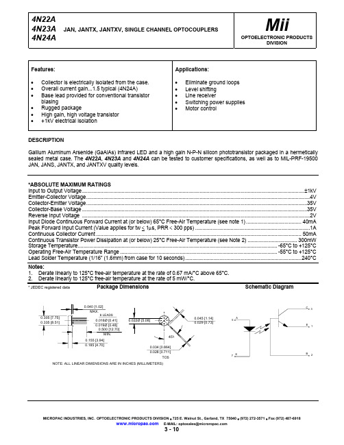
元器件交易网 4N22A, 4N23A, and 4N24A
JAN, JANTX, JANTXV, SINGLE CHANNEL OPTOCOUPLERS
*ELECTRICAL CHARACTERISTICS INPUT LED TA = 25°C Unless otherwise specified
4N22A
1
4N23A
IC(ON)
2.5
4N24A
4
On State Collector Current +100°C
4N22A
1
4N23A
IC(ON)
2.5
4N24A
4
Off State Collector Current Off State Collector Current
+25°C +100°C
V(BR)CBO
35
V(BR)CEO
35
V(BR)EBO
4
MAX
UNITS
V V V
TEST CONDITIONS
IC = 100µA, IB = 0, IF = 0 IC = 1mA, IB = 0, IF = 0 IC = 0, IE = 100µA, IF = 0
NOTE
*COUPLED CHARACTERISTICS TA = 25°C Unless otherwise specified
*ABSOLUTE MAXIMUM RATINGS Input to Output Voltage.............................................................................................................................................................±1kV Emitter-Collector Voltage..............................................................................................................................................................4V Collector-Emitter Voltage............................................................................................................................................................35V Collector-Base Voltage ...............................................................................................................................................................35V Reverse Input Voltage .................................................................................................................................................................2V Input Diode Continuous Forward Current at (or below) 65°C Free-Air Temperature (see note 1) ....................................... 40mA Peak Forward Input Current (Value applies for tw < 1µs, PRR < 300 pps) .................................................................................1A Continuous Collector Current ................................................................................................................................................. 50mA Continuous Transistor Power Dissipation at (or below) 25°C Free-Air Temperature (see Note 2) ................................... 300mW Storage Temperature............................................................................................................................................. -65°C to +125°C Operating Free-Air Temperature Range ............................................................................................................... -55°C to +125°C Lead Solder Temperature (1/16” (1.6mm) from case for 10 seconds) ..................................................................................240°C
2N720AS中文资料

Applications
• General purpose • Low power • NPN silicon transistor
Features
• • • • Hermetically sealed TO-18 metal can Also available in chip configuration Chip geometry 4500 Reference document: MIL-PRF-19500/182
2N720A
Silicon NPN Transistor
Data Sheet
ELECTRICAL CHARACTERISTICS
characteristics specified at TA = 25°C
Off Characteristics Parameter Collector-Emitter Breakdown Voltage Collector-Emitter Breakdown Voltage Collector-Base Cutoff Current Emitter-Base Cutoff Current On Characteristics Parameter Symbol hFE1 hFE2 hFE3 hFE4 VBEsat VCEsat Symbol V(BR)CEO V(BR)CER ICBO1 ICBO2 ICBO3 IEBO1 IEBO2 Test Conditions IC = 30 mA IC = 10 mA, RBE = 10 Ω VCB = 120 Volts VCB = 90 Volts VCE = 90 Volts, TA = 150 OC VEB = 7 Volts VEB = 5 Volts Min 80 100 100 10 15 100 10 Typ Max Units Volts Volts µA nA µA µA nA
JANTXV2N6676中文资料
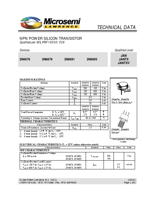
6 Lake Street, Lawrence, MA 01841 1-800-446-1158 / (978) 794-1666 / Fax: (978) 689-0803
120101 Page 2 of 2
W W 0 C Unit C/W
THERMAL CHARACTERISTICS
Characteristics Thermal Resistance, Junction-to-Case 1) Derate linearly 1.0 W/0C for TC > 250C 2) Derate linearly 34.2 mW/0C for TA > 250C 3) Derate linearly 17.1 mW/0C for TA > 250C
ON CHARACTERISTICS (4)
hFE VCE(sat) VBE(sat)
15 8.0
40 20 1.0 1.5 Vdc Vdc
DYNAMIC CHARACTERISTICS
Small-Signal Short-Circuit Forward Current Transfer Ratio IC = 1.0 Adc; VCE = 10 Vdc, f = 5 MHz Output Capacitance VCB = 10 Vdc; IE = 0, 100 kHz ≤ f ≤ 1.0 MHz hfe Cobo
MAXIMUM RATINGS
Ratings Collector-Emitter Voltage Collector-Base Voltage Collector-Base Voltage Emitter-Base Voltage Base Current Collector Current Symbol VCEO VCBO VCEX VEBO IB IC 2N6676 2N6678 2N6691 2N6693 300 400 450 650 450 650 8.0 5.0 15 2N6676 2N6691 2N6678 2N6693 6.0(2) 3.0(3) 175 175 -65 to +200 Max. 1.0 Unit Vdc Vdc Vdc Vdc Adc Adc
JANSF2N7389U中文资料

-100 - 2.0
— — — —
—
—
—
-100 —
V
- 4.0 -2.0 -5.0
-100 100
— -100 nA — 100
-25
— -25 µA
0.259
— 0.259 Ω
BVDSS VGS(th) IGSS IGSS IDSS RDS(on)
RDS(on)
VSD
Drain-to-Source Breakdown Voltage Gate Threshold Voltage Gate-to-Source Leakage Forward Gate-to-Source Leakage Reverse Zero Gate Voltage Drain Current Static Drain-to-Source ➃ On-State Resistance (TO-3) Static Drain-to-Source ➃ On-State Resistance (LCC-18) Diode Forward Voltage ➃
QRR Reverse Recovery Charge
— — 0.74 µC
VDD ≤ -25V ➃
ton Forward Turn-On Time
Intrinsic turn-on time is negligible. Turn-on speed is substantially controlled by LS + LD.
Gate-to-Source Leakage Forward Gate-to-Source Leakage Reverse Total Gate Charge Gate-to-Source Charge Gate-to-Drain (‘Miller’) Charge Turn-On Delay Time Rise Time Turn-Off Delay Time Fall Time Total Inductance
- 1、下载文档前请自行甄别文档内容的完整性,平台不提供额外的编辑、内容补充、找答案等附加服务。
- 2、"仅部分预览"的文档,不可在线预览部分如存在完整性等问题,可反馈申请退款(可完整预览的文档不适用该条件!)。
- 3、如文档侵犯您的权益,请联系客服反馈,我们会尽快为您处理(人工客服工作时间:9:00-18:30)。
Collector-Emitter Breakdown Voltage IC = 200 mAdc; L = 14 mH; F = 30-60 Hz; RBE = 50Ω (See Figure 3 of MIL-PRF-19500/510) 2N6249 2N6250 2N6251 Emitter-Base Cutoff Current VEB = 6 Vdc Collector-Emitter Cutoff Current VCE = 150 Vdc 2N6249 VCE = 225 Vdc 2N6250 VCE = 300 Vdc 2N6251
6 Lake Street, Lawrence, MA 01841 1-800-446-1158 / (978) 794-1666 / Fax: (978) 689-0803
120101 Page 2 of 2
MAXIMUM RATINGS Ratings
Collector-Emitter Voltage Collector-Base Voltage Emitter-Base Voltage Collector Current Base Current Total Power Dissipation @ TA = +250C (1) @ TC = +250C (2) Operating & Storage Temp Range
hfe
2.5 Cobo 15 500 pF
SWITCHING CHARACTERISTICS
Turn-On Time VCC = 200 Vdc; IC = 10 Adc IB = 1.0 Adc IB = 1.25 Adc IB = 1.67 Adc Turn-Off Time VCC = 200 Vdc; IC = 10 Adc IB = 1.0 Adc IB = 1.25 Adc IB = 1.67 Adc 2N6249 2N6250 2N6251
THERMAL CHARACTERISTICS
Characteristics Symbol Thermal Resistance, Junction-to-Case RθJC 1) Derate linearly at 34.2 mW/0C for TA > +250C 2) Derate linearly at 1.0 W/0C for TC > +250C
Vdc
DYNAMIC CHARACTERISTICS
Magnitude of Small-Signal Short-Circuit Forward Current Transfer Ratio IC = 1.0 Adc, VCE = 10 Vdc, f = 1 MHz Output Capacitance VCB = 10 Vdc, IC = 0, 100 kHz ≤ f ≤ 1.0 MHz
ICBO
mAdc
ON CHARACTERISTICS(3)
2N6249 2N6250 2N6251 2N6249 2N6250 2N6251 2N6249 2N6250 2N6251
hFE
10 8 6
50 50 50 1.5 1.5 1.5 2.25 2.25 2.25 Vdc
VCE(sat)
VBE(sat)
V(BR)CER
225 300 375 100 1.0 1.0 1.0
Vdc
IEBO
µAdc
ICEO
mAdc
6 Lake Street, Lawrence, MA 01841 1-800-446-1158 / (978) 794-1666 / Fax: (978) 689-0803
120101 Page 1 of 2
Collector-Emitter Cutoff Current VCE = 225 Vdc; VBE = -1.5 Vdc VCE = 300 Vdc; VBE = -1.5 Vdc VCE = 375 Vdc; VBE = -1.5 Vdc Collector-Base Cutoff Current VCB = 300 Vdc VCB = 375 Vdc VCB = 450 Vdc Forward-Current Transfer Ratio IC = 10 Adc; VCE = 3 Vdc Collector-Emitter Saturated Voltage IB = 1.0 Adc; IC = 10 Adc IB = 1.25 Adc; IC = 10 Adc IB = 1.67 Adc; IC = 10 Adc Base-Emitter Saturated Voltage IB = 1.0 Adc; IC = 10 Adc IB = 1.25 Adc; IC = 10 Adc IB = 1.67 Adc; IC = 10 Adc 2N6249 2N6250 2N6251 2N6249 2N6250 2N6251 ICEX 100 100 100 0.5 0.5 0.5 µAdc
t
on
2.0 2.0 2.0
µs
2N6249 2N6250 2N6251
t
off
4.5 4.5 4.5
µs
SAFE OPERATING AREA
DC Tests TC = +250C; t = 1 s, 1 cycle (See Figure 5 of MIL-PRF-19500/510) Test 1 VCE = 17.5 Vdc, IC = 10 Adc Test 2 VCE = 30 Vdc, IC = 5.8 Adc Test 3 VCE = 100 Vdc, IC = 0.3 Adc 3) Pulse Test: Pulse Width = 300µs, Duty Cycle ≤ 2.0%.
元器件交易网
TECHNICAL DATA
NPN POWER SILICON TRANSISTOR
Qualified per MIL-PRF-19500/510 Devices 2N6249 2N6250 2N6251 Qualified Level JAN JANTX JANTXV JANHC
元器件交易网
2N6249, 2N6250, 2N6251 JAN SERIES
ELECTRICAL CHARACTERISTICS (con’t)
Characteristics Symbol Min. Max. Unit
OFF CHARACTERISTICS (con’t)
Symbol 2N6249 2N6250
VCEO VCBO VEBO IC IB PT Top, Tstg 200 300 275 375 6.0 10 5.0 5.5 175 -55 to +200 Max. 1.0
2N6251 350 450
Units
Vdc Vdc Vdc Adc Adc W W 0 C Unit C/W
OFF CHARACTERISTICS
Collector-Emitter Breakdown Voltage IC = 200 mAdc; L = 42 mH; F 30-60 Hz (See Figure 3 of MIL-PRF-19500/510) 2N6249 2N6250 2N6251 V(BR)CEO 200 275 350 Vdc
0
TO-3 (TO-204AA)*
*See Appendix A for Package Outline
ELECTRICAL CHARACTERISTICS (TA = 250C unless otherwise noted)
Characteristics Symbol Min. Max. Unit
