CMBZ-5232B中文资料
MMSZ5242BT1中文资料

MMSZ5221BT1 SeriesPreferred DeviceZener Voltage Regulators 500 mW SOD−123 Surface MountThree complete series of Zener diodes are offered in the convenient, surface mount plastic SOD−123 package. These devices provide a convenient alternative to the leadless 34−package style.Features•500 mW Rating on FR−4 or FR−5 Board•Wide Zener Reverse V oltage Range − 2.4 V to 110 V •Package Designed for Optimal Automated Board Assembly •Small Package Size for High Density Applications •General Purpose, Medium Current•ESD Rating of Class 3 (>16 kV) per Human Body Model•Pb−Free Packages are AvailableMechanical CharacteristicsCASE:V oid-free, transfer-molded, thermosetting plastic case FINISH:Corrosion resistant finish, easily solderableMAXIMUM CASE TEMPERATURE FOR SOLDERING PURPOSES: 260°C for 10 SecondsPOLARITY:Cathode indicated by polarity band FLAMMABILITY RATING:UL 94 V−0MAXIMUM RATINGSMaximum ratings are those values beyond which device damage can occur. Maximum ratings applied to the device are individual stress limit values (not normal operating conditions) and are not valid simultaneously. If these limits are exceeded, device functional operation is not implied, damage may occur and reliability may be affected.1.FR−5 = 3.5 X 1.5 inches, using the minimum recommended footprint.2.Thermal Resistance measurement obtained via infrared Scan Method.See specific marking information in the device marking column of the Electrical Characteristics table on page 3 of this data sheet.DEVICE MARKING INFORMATIONDevices listed in bold, italic are ON Semiconductor Preferred devices. Preferred devices are recommended choices for future use and best overall value.ELECTRICAL CHARACTERISTICS (T A = 25°C unlessotherwise noted, V= 0.95 V Max. @ I = 10 mA)4.Nominal Zener voltage is measured with the device junction in thermal equilibrium at T L = 30°C $1°C.5.Z ZT and Z ZK are measured by dividing the AC voltage drop across the device by the ac current applied.The specified limits are for I Z(AC) = 0.1 I Z(dc) with the AC frequency = 1 KHz.V Z , NOMINAL ZENER VOLTAGE (V)−1012345678Figure 1. Temperature Coefficients (Temperature Range −55°C to +150°C)100101V Z , NOMINAL ZENER VOLTAGE (V)Figure 2. Temperature Coefficients (Temperature Range −55°C to +150°C)1.21.00.80.60.40.20T, TEMPERATURE (°C)Figure 3. Steady State Power Derating PW, PULSE WIDTH (ms)Figure 4. Maximum Nonrepetitive Surge Power1000100101V Z , NOMINAL ZENER VOLTAGEFigure 5. Effect of Zener Voltage onZener Impedance100101V F , FORWARD VOLTAGE (V)Figure 6. Typical Forward Voltage1000100101q V Z , T E M P E R A T U R E C O E F F I C I E N T (m V /°C )q V Z , T E M P E R A T U R E C O E F F I C I E N T (m V /°C )P p k , P E A K S U R G E P O W E R (W A T T S )Z Z T , D Y N A M I C I M P E D A N C E (W )I F , F O R W A R D C U R R E N T (m A )C , C A P A C I T A N C E (p F )V Z , NOMINAL ZENER VOLTAGE (V)Figure 7. Typical Capacitance 1000100101V Z , ZENER VOLTAGE (V)1001010.10.01V Z , ZENER VOLTAGE (V)1001010.10.01V Z , NOMINAL ZENER VOLTAGE (V)Figure 8. Typical Leakage CurrentFigure 9. Zener Voltage versus Zener Current(V Z Up to 12 V)Figure 10. Zener Voltage versus Zener Current(12 V to 91 V)I R , L E A K A G E C U R R E N T (m A )I Z , Z E N E R C U R R E N T (m A )I Z , Z E N E R C U R R E N T (m A )PACKAGE DIMENSIONSSOD−123CASE 425−04ISSUE Cǒmm inchesǓSCALE 10:1*For additional information on our Pb−Free strategy and solderingdetails, please download the ON Semiconductor Soldering and Mounting Techniques Reference Manual, SOLDERRM/D.SOLDERING FOOTPRINT*ON Semiconductor and are registered trademarks of Semiconductor Components Industries, LLC (SCILLC). SCILLC reserves the right to make changes without further notice to any products herein. SCILLC makes no warranty, representation or guarantee regarding the suitability of its products for any particular purpose, nor does SCILLC assume any liability arising out of the application or use of any product or circuit, and specifically disclaims any and all liability, including without limitation special, consequential or incidental damages.“Typical” parameters which may be provided in SCILLC data sheets and/or specifications can and do vary in different applications and actual performance may vary over time. All operating parameters, including “Typicals” must be validated for each customer application by customer’s technical experts. SCILLC does not convey any license under its patent rights nor the rights of others. SCILLC products are not designed, intended, or authorized for use as components in systems intended for surgical implant into the body, or other applications intended to support or sustain life, or for any other application in which the failure of the SCILLC product could create a situation where personal injury or death may occur. Should Buyer purchase or use SCILLC products for any such unintended or unauthorized application, Buyer shall indemnify and hold SCILLC and its officers, employees, subsidiaries, affiliates,and distributors harmless against all claims, costs, damages, and expenses, and reasonable attorney fees arising out of, directly or indirectly, any claim of personal injury or death associated with such unintended or unauthorized use, even if such claim alleges that SCILLC was negligent regarding the design or manufacture of the part. SCILLC is an Equal Opportunity/Affirmative Action Employer. This literature is subject to all applicable copyright laws and is not for resale in any manner.PUBLICATION ORDERING INFORMATION。
CMBP系列贴片铁氧体磁珠商品说明书

●EXTERNAL DIMENSIONS UNIT:mm(外形尺寸)
PART NO. CMBP0402 CMBP0603 CMBP0805 CMBP1206
A 1.0±0.15 1.6±0.15 2.0(+0.3,-0.1) 3.2±0.2
B 0.5±0.15 0.8±0.15 1.25±0.2 1.6±0.2
CMBP0603- 600 60±25%
CMBP0603- 750 75±25%
CMBP0603- 121 120±25%
CMBP0603- 221 220±25%
CMBP0603- 601 600±25%
MHz Freq, 100 100 100 100 100 100
CMBP0805 TYPE
Max.DC Resistance 直流电阻
Design As Customers Requested Specifications 可根据客户需求设计
电感专业制造商 CMBP系列贴片铁氧体磁珠
CMBP0402 TYPE
Part Number 型号
Inductance 阻抗
Z Test Frequency
阻抗的测试频率
Units 单位 Symbol 符号 CMBP0402- 100
抑制效果,两种铁氧体材料、阻抗范围宽。适用于不同的电子线路 Internal silver printed layers and magnetic shielded structures to minimize crosstalk,Can be used in a wide range of frequency(from dozens of MHz to hundreds of MHz)to suppress EMI,Two types material and wide range of impedance values for various applications
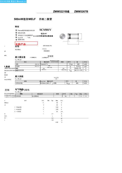
ZMM5235B中文资料(SynSemi)中文数据手册「EasyDatasheet - 矽搜」

16
7.8
17
600
0.1
12
ZMM5247B
17
7.4
19
600
0.1
13
ZMM5248B
18
7.0
21
600
0.1
14
ZMM5249B
19
6.6
23
600
0.1
14
ZMM5250B
20
6.2
25
600
0.1
15
ZMM5251B
22
5.6
29
600
0.1
17
ZMM5252B
24
5.2
33
600
0.1
80
800
0.1
30
ZMM5260B
43
3.0
93
900
0.1
33
ZMM5261B
47
2.7
105
1000
0.1
36
ZMM5262B
51
2.5
125
1100
0.1
39
ZMM5263B
56
2.2
150
1300
0.1
43
ZMM5264B
60
2.1
170
1400
0.1
46
ZMM5265B
62
2.0
185
1400
安装焊盘布局
0.098 (2.50) Max.
0.197 (5.00) REF
尺寸以英寸(毫米)
0.079 (2.00)Min.
最大额定值和热特性
等级25
°C环境温度,除非另有specifie.
DL5232B中文资料

DC COMPONENTS CO., LTD.
R
DL5221B THRU DL5259B
RECTIFIER SPECIALISTS
TECHNICAL SPECIFICATIONS OF GLASS SILICON ZENER DIODES
FEATURES
* Voltage Range:2.4V to 39V * Double slug type construction
SYMBOL Zener Current see Table "Characterisitics" Power Dissipation at Tamb=25 oC Junction Temperature Storage Temperature Range Ptot Tj Tstg
VALUE 500 (1) 175 -55 to + 175
DL-35
MECHANICAL DATA
* Case: Glass case Minimelf DL-35 * Terminals:Solder plated, solderable per MIL-STD-750, Method 2026 * Polarity: Color band denotes cathode end * Mounting position: Any * Weight: 0.05 gram Approx.
298
NEXT NEXT NEXT
EXIT EXI BACK BACK EXIT BACK
元器件交易网
RATING AND CHARACTERISTIC CURVES (DL5221B THRU DL5259B)
Nominal Zener Voltage VZ@IZT Volts
ZLB系列产品说明书
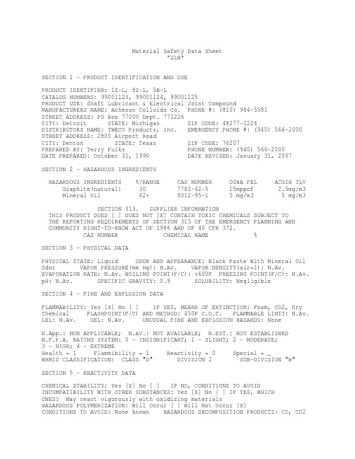
Material Safety Data Sheet*ZLB*SECTION 1 - PRODUCT IDENTIFICATION AND USEPRODUCT IDENTIFIER: 1Z-L, 8Z-L, 5B-LCATALOG NUMBERS: 99001123, 99001124, 99001125PRODUCT USE: Shaft Lubricant & Electrical Joint CompoundMANUFACTURERS NAME: Acheson Colloids Co. PHONE #: (810) 984-5581STREET ADDRESS: PO Box 77000 Dept. 771226CITY: Detroit STATE: Michigan ZIP CODE: 48277-1226DISTRIBUTORS NAME: TWECO Products, Inc. EMERGENCY PHONE #: (940) 566-2000STREET ADDRESS: 2800 Airport RoadCITY: Denton STATE: Texas ZIP CODE: 76207PREPARED BY: Terry Fulks PHONE NUMBER: (940) 566-2000 DATE PREPARED: October 31, 1990 DATE REVISED: January 31, 2007SECTION 2 - HAZARDOUS INGREDIENTSHAZARDOUS INGREDIENTS %/RANGE CAS NUMBER OSHA PEL ACGIH TLVGraphite(natural) 30 7782-42-5 15mppcf 2.5mg/m3 Mineral Oil 62+ 8012-95-1 5 mg/m3 5 mg/m3SECTION 313. SUPPLIER INFORMATIONTHIS PRODUCT DOES [ ] DOES NOT [X] CONTAIN TOXIC CHEMICALS SUBJECT TOTHE REPORTING REQUIREMENTS OF SECTION 313 OF THE EMERGENCY PLANNING ANDCOMMUNITY RIGHT-TO-KNOW ACT OF 1986 AND OF 40 CFR 372.CAS NUMBER CHEMICAL NAME %SECTION 3 - PHYSICAL DATAPHYSICAL STATE: Liquid ODOR AND APPEARANCE: Black Paste With Mineral OilOdor VAPOR PRESSURE(mm Hg): N.Av. VAPOR DENSITY(air=1): N.Av.EVAPORATION RATE: N.Av. BOILING POINT(F/C): >600F FREEZING POINT(F/C): N.Av.pH: N.Av. SPECIFIC GRAVITY: 0.9 SOLUBILITY: NegligibleSECTION 4 - FIRE AND EXPLOSION DATAFLAMMABILITY: Yes [X] No [ ] IF YES, MEANS OF EXTINCTION: Foam, CO2, DryChemical FLASHPOINT(F/C) AND METHOD: 450F C.O.C. FLAMMABLE LIMIT: N.Av.LEL: N.Av. UEL: N.Av. UNUSUAL FIRE AND EXPLOSION HAZARDS: NoneN.App.: NON APPLICABLE; N.AV.: NOT AVAILABLE; N.EST.: NOT ESTABLISHEDN.F.P.A. RATING SYSTEM: 0 - INSIGNIFICANT; 1 - SLIGHT; 2 - MODERATE;3 - HIGH;4 - EXTREMEHealth = 1 Flammibility = 1 Reactivity = 0 Special = _WHMIS CLASSIFICATION: CLASS "D" DIVISION 2 SUB-DIVISION "B"SECTION 5 - REACTIVITY DATACHEMICAL STABILITY: Yes [X] No [ ] IF NO, CONDITIONS TO AVOIDINCOMPATIBILITY WITH OTHER SUBSTANCES: Yes [X] No [ ] IF YES, WHICHONES? May react vigorously with oxidizing materialsHAZARDOUS POLYMERIZATION: Will Occur [ ] Will Not Occur [X]CONDITIONS TO AVOID: None known HAZARDOUS DECOMPOSITION PRODUCTS: CO, CO2ZLB Page 2SECTION 6 - HEALTH HAZARD DATAROUTE OF ENTRY: SKIN CONTACT [ ] SKIN ABSORPTION [X] EYE CONTACT [X]INHALATION [X] INGESTION [ ]EFFECTS OF ACUTE/CHRONIC EXPOSURE TO PRODUCT: Irritation of the eyes,Dermatitis CARCINOGENICITY: No SIGNS AND SYMPTOMS OF EXPOSURE: Irritationof the skin and eyes MEDICAL CONDITIONS GENERALLY AGGRAVATED BY EXPOSURE: Pre-existing skin disorders EMERGENCY AND FIRST AID PROCEDURES: SKIN: Washthoroughly with soap and water EYES: Flush immediately with water for15 minutes, get medical attention. INGESTION: No ill effects expectedINHALATION: No ill effects expectedSECTION 7 - PRECAUTIONS FOR SAFE HANDLING AND USELEAK AND SPILL PROCEDURE: Remove any source of ignition, scoop up as much aspossible, cover remainder with absorbent material & place in non-leakingcontainer for disposal. WASTE DISPOSAL METHOD: Dispose of in accordance withFederal, State & Local regulationsPRECAUTIONS TO BE TAKEN IN HANDLING AND STORING: Store away from sparks, openflames, or excessive heatSECTION 8 - CONTROL MEASURESRESPIRATORY PROTECTION: Not needed for this product. As required for cuttingand welding. GLOVES: Oil resistant RESPIRATOR: not needed EYE: Safetyor chemical goggles FOOTWEAR: N.App. CLOTHING: As required for weldingOTHER: N.Est.VENTILATION: Not normally needed WORK/HYGIENIC PRACTICES: Normal HygieneREFERENCES:"Chemical Guide To OSHA Hazard Communication Standard" First Edition"Handbook Of Toxic And Hazardous Chemicals and Carcinogens" Second Edition "Registry Of Toxic Effects Of Chemical Substances""NIOSH Pocket Guide to CHEMICAL HAZARDS" June 1994THIS DATA IS OFFERED IN GOOD FAITH AS TYPICAL VALUES. THIS IS NEITHER ANEXPRESSED NOR IMPLIED PRODUCT SPECIFICATION. RECOMMENDED HANDLING PROCEDURESAND HYGIENE ARE BELIEVED TO BE ACCURATE, HOWEVER, THESE RECOMMENDATIONS SHOULDBE REVIEWED IN THE SPECIFIC CONTEXT OF INTENDED USE AND DETERMINED APPROPRIATEBY THE USER.。
MMSZ5231中文资料

NEW PRODUCT
NEW PRODUCT
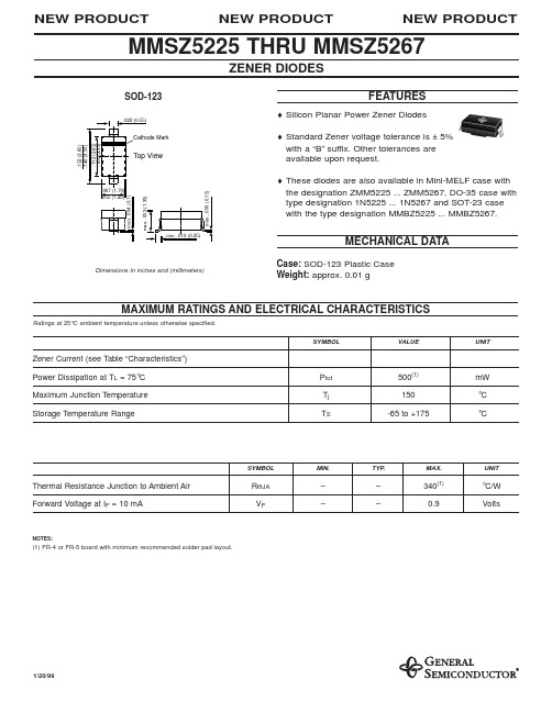
MMSZ5225 THRU MMSZ5267
ZENER DIODES
SOD-123
.022 (0.55)
FEATURES
♦ Silicon Planar Power Zener Diodes ♦ Standard Zener voltage tolerance is ± 5% with a “B” suffix. Other tolerances are available upon request. ♦ These diodes are also available in Mini-MELF case with the designation ZMM5225 ... ZMM5267, DO-35 case with type designation 1N5225 ... 1N5267 and SOT-23 case with the type designation MMBZ5225 ... MMBZ5267.
(%/K)
IR (µA)
Test Voltage VR (V)
MMSZ5225 MMSZ5226 MMSZ5227 MMSZ5228 MMSZ5229 MMSZ5230 MMSZ5231 MMSZ5232 MMSZ5233 MMSZ5234 MMSZ5235 MMSZ5236 MMSZ5237 MMSZ5238 MMSZ5239 MMSZ5240 MMSZ5241 MMSZ5242 MMSZ5243 MMSZ5244 MMSZ5245 MMSZ5246 MMSZ5247 MMSZ5248 MMSZ5249 MMSZ5250 MMSZ5251 MMSZ5252 MMSZ5253 MMSZ5254 MMSZ5255 MMSZ5256 MMSZ5257 MMSZ5258 MMSZ5259 MMSZ5260 MMSZ5261 MMSZ5262 MMSZ5263 MMSZ5264 MMSZ5265 MMSZ5266 MMSZ5267
MMSZ5232BS-7-F中文资料

Lead-free·Planar Die Construction·Ultra-Small Surface Mount Package ·General Purpose·Ideally suited for Automated Assembly Processes ·Lead Free /RoHS Compliant (Note 3)FeaturesMaximum Ratings@ T A = 25°C unless otherwise specifiedNotes: 1. Part mounted on FR-4 PC board with recommended pad layout, which can be found on our website at /datasheets/ap02001.pdf.2. Short duration pulse test used to minimize self-heating effect.3. No purposefully added lead.Mechanical DataMMSZ5221BS - MMSZ5259BSSURFACE MOUNT ZENER DIODE·Case: SOD-323·Case Material: Molded Plastic. UL Flammability Classification Rating 94V-0·Moisture Sensitivity: Level 1 per J-STD-020C ·Terminals: Solderable per MIL-STD-202, Method 208·Lead Free Plating (Matte Tin Finish annealed over Alloy 42leadframe). Please see Ordering Information, Note 5, on Page 2·Polarity: Cathode Band ·Marking: See Page 2·Weight: 0.004 grams (approximate)Electrical Characteristics@ T A = 25°C unless otherwise specified5. f = 1KHz.XX = Product Type Marking Code (See Table Above)Marking InformationOrdering Information (Note 6)Notes: 6. For Packaging Details, go to our website at: /datasheets/ap02007.pdf.*Add “-7-F” to the appropriate type number in Table 1 above example: 6.2V Zener = MMSZ5234BS-7-F.0102030I , Z E N E R C U R R E N T (m A )Z V , ZENER VOLTAGE (V)Z Fig. 6 Zener Breakdown Characteristics10203040102030405012345678910I , ZE N E R C U R R E N T (m A )Z V , ZENER VOLTAGE (V)Z Fig. 5 Zener Breakdown Characteristics110100110100P , P E A K S U R G E P O W E R (W )P K PULSE WIDTH (ms)Fig. 4 Maximum Non-repetitive Surge Power10001101001000110100V , NOMINAL ZENER VOLTAGE (V)Z Fig. 3 Zener Impedance vs. Zener Voltage1101001000110100C , T O T A L C A P A C I T A N C E (p F )T V , NOMINAL ZENER VOLTAGE (V)Z Fig. 2 Typical Capacitance00.10.20.30.4255075100125150P , P O W E R D I S S I P A T I O N (W )D T , AMBIENT TEMPERATURE (°C)A Fig. 1 Power Dissipation vs Ambient TemperatureIMPORTANT NOTICEDiodes Incorporated and its subsidiaries reserve the right to make modifications, enhancements, improvements, corrections or other changes without further notice to any product herein. Diodes Incorporated does not assume any liability arising out of the application or use of any product described herein; neither does it convey any license under its patent rights, nor the rights of others. The user of products in such applications shall assume all risks of such use and will agree to hold Diodes Incorporated and all the companies whose products are represented on our website, harmless against all damages.LIFE SUPPORTDiodes Incorporated products are not authorized for use as critical components in life support devices or systems without the expressed written approval of the President of Diodes Incorporated.。
DL5244B-TP;DL5230B-TP;DL5242B-TP;DL5231B-TP;DL5232B-TP;中文规格书,Datasheet资料

DL5221THRU DL5267500 mW Zener Diode 2.4 to 75 VoltsFeatures• Wide Voltage Range Available • Glass Package• High Temp Soldering: 260°C for 10 Seconds At Terminals • Surface Mount Packageomp onents 20736 Marilla Street Chatsworth! "# $ % ! "#Marking : Cathode band denotes polarityMicro Commercial Components•Lead Free Finish/RoHS Compliant(Note 1) ("P" Suffix designates Note:1.Lead in Glass Exemption Applied, see EU Directive Annex 5.MCC PART NUMBER NOMINAL ZENER VOLTAGE V Z @ I ZTTESTCURRENT I ZTMAXIMUM ZENER IMPEDANCE‘B’ SUFFIX ONLYZ ZT @ I ZT Z ZK @I ZK = 0.25mA MAXIMUM REVERSE LEAKAGE CURRENTI R @ V R MAX. ZENER VOLTAGE TEMP COEFFICIENT ‘B’SUFFIX ONLYVOLTS mA OHMS OHMS µA VOLTS % / °CDL5221 2.420301200100 1.0-0.085DL5222 2.520301250100 1.0-0.085DL5223 2.72030130075 1.0-0.080DL5224 2.82030140075 1.0-0.080DL5225 3.020******** 1.0-0.075DL5226 3.32028160025 1.0-0.070DL5227 3.62024170015 1.0-0.065DL5228 3.92023190010 1.0-0.060DL5229 4.320222000 5.0 1.0±0.055DL5230 4.720191900 5.0 2.0±0.030DL5231 5.120171600 5.0 2.0±0.030DL5232 5.620111600 5.0 3.0+0.038DL5233 6.0207.01600 5.0 3.5+0.038DL5234 6.2207.01000 5.0 4.0+0.045DL5235 6.820 5.0750 3.0 5.0+0.050DL52367.520 6.0500 3.0 6.0+0.058DL52378.2208.0500 3.0 6.5+0.062DL52388.7208.0600 3.0 6.5+0.065DL52399.12010600 3.07.0+0.068DL5240102017600 3.08.0+0.075DL5241112022600 2.08.4+0.076DL5242122030600 1.09.1+0.077DL5243139.5136000.59.9+0.079DL5244149.0156000.110+0.082DL5245158.5166000.111+0.082DL5246167.8176000.112+0.083DL5247177.4196000.113+0.084DL5248187.0216000.114+0.085DL524919 6.6236000.114+0.086DL525020 6.2256000.115+0.086DL525122 5.6296000.117+0.087DL525224 5.2336000.118+0.088DL525325 5.0356000.119+0.089DL525427 4.6416000.121+0.090DL525528 4.5446000.121+0.091DL525630 4.2496000.123+0.091DL525733 3.8587000.125+0.092DL525836 3.4707000.127+0.093DL525939 3.2808000.130+0.094DL526043 3.0939000.133+0.095DL526147 2.710510000.136+0.095DL526251 2.512511000.139+0.096DL526356 2.215013000.143+0.096DL526460 2.117014000.146+0.097DL526562 2.018514000.147+0.097DL526668 1.823016000.152+0.097DL5267751.727017000.156+0.098NOTE 1: Table as shown lists type numbers, which indicate a tolerance of ±20% with guaranteed limits on only Vz, I R , and V F . Devices withguaranteed limits on all six parameters are indicated by suffix “A”for ±10%, “B”for ±5%, “C”for ±2% toleranceNOTE 2: The electrical characteristics are measured after allowing the device to stabilize for 20 seconds.NOTE 3: Temperature coefficient (áVZ ). Test conditions for temperature coefficient are as follows:a.I ZT = 7.5mA, T I = 25o C T 2 = 125o C (DL5221 thru DL5242)b.I ZT = Rated I ZT ,T I = 25o C,T 2= 125o C (DL5243 thru DL5267)Device to be temperature stabilized with current applied prior to reading breakdown voltage at the specified ambient temperature.DL5221 thru DL5267Micro Commercial ComponentsCharacteristics (T j =25ćunless otherwise specified)Micro Commercial ComponentsDL5221 thru DL5267Figure 1. Zener Voltage versus Zener Current – Vz=1 thru 16 VoltsFigure 2. Zener Voltage versus Zener Current – Vz=15 thru 30 VoltsFigure 3. Zener Voltage versus Zener Current – Vz=30 thru 75 VoltsFigure 4. Thermal resistance from junction to ambient as a function of pulse durationMicro Commercial ComponentsCharacteristics (T j =25℃ unless otherwise specified) DL5221 thru DL5267Micro Commercial ComponentsOrdering Information :Device PackingPart Number-TP Tape&Reel: 2.5Kpcs/Reel***IMPORTANT NOTICE***Micro Commercial Components Corp. reserve s the right to make changes without further notice to any product herein to make corrections, modifications , enhancements , improvements , or other changes . Micro Commercial Components Corp . does not assume any liability arising out of the application or use of any product described herein; neither does it convey any license under its patent rights ,nor the rights of others . The user of products in such applications shall assume all risks of such use and will agree to hold Micro Commercial Components Corp . and all the companies whose products are represented on our website, harmless against all damages.***LIFE SUPPORT***MCC's products are not authorized for use as critical components in life support devices or systems without the express writtenapproval of Micro Commercial Components Corporation.***CUSTOMER AWARENESS***Counterfeiting of semiconductor parts is a growing problem in the industry. Micro Commercial Components (MCC) is taking strong measures to protect ourselves and our customers from the proliferation of counterfeit parts. MCC strongly encourages customers to purchase MCC parts either directly from MCC or from Authorized MCC Distributors who are listed by country on our web page cited below. Products customers buy either from MCC directly or from Authorized MCC Distributors are genuine parts, have full traceability, meet MCC's quality standards for handling and storage. MCC will not provide any warranty coverage or other assistance for parts bought from Unauthorized Sources. MCC is committed to combat this global problem and encourage our customers to do their part in stopping this practice by buying direct or from authorized distributors.分销商库存信息:MICRO-COMMERICAL-CODL5244B-TP DL5230B-TP DL5242B-TP DL5231B-TP DL5232B-TP DL5239B-TP DL5250B-TP DL5253B-TP DL5233B-TP DL5234B-TP DL5238B-TP DL5240B-TP DL5243B-TP DL5248B-TP DL5249B-TP DL5255B-TP DL5226B-TP DL5235B-TP DL5227B-TP DL5228B-TP DL5229B-TP DL5236B-TP DL5237B-TP DL5241B-TP DL5245B-TP DL5246B-TP DL5247B-TP DL5251B-TP DL5252B-TP DL5254B-TP DL5256B-TP DL5257B-TP DL5221B-TP DL5222B-TP DL5223B-TP DL5224B-TP DL5225B-TP DL5258B-TP DL5259B-TP DL5260B-TP DL5261B-TP DL5262B-TP DL5263B-TP DL5264B-TP DL5265B-TP DL5266B-TP DL5267B-TP。
ZD5232A中文资料(Cystech Electonics)中文数据手册「EasyDatasheet - 矽搜」

3.0
6.0
3.0
6.5
3.0
6.5
3.0
7.0
3.0
8.0
2.0
8.4
1.0
9.1
0.5
9.9
0.1
11
0.1
12
0.1
14
0.1
15
0.1
17
0.1
18
0.1
21
0.1
21
0.1
23
0.1
25
0.1
27
0.1
30
0.1
33
芯片中文手册,看全文,戳
规格.编号:C326SH 发布日期:2009.10.07
ZD5252A K2 24 23.52 24.48 33 5.2 600
ZD5254A K4 27 26.46 27.54 41 5.0 600
ZD5255A K5 28 27.44 28.56 44 4.5 600
ZD5256A M1 30 29.40 30.60 49 4.2 600
ZD5257A M2 33 32.34 33.66 58 3.8 700
°C
最大正向电压@ I
F=10mA ………………………………………………………........0.9V
最大功率耗散
总功率耗散@T 热阻,结到环境空气ř
L=75 °C Ptot (注1) ................................................... 500毫瓦
ZD5223A C3 2.7 2.65 2.75
30 20 1300
ZD5225A C5 3.0 2.94 3.06
30 20 1600
CMBZ-5252B中文资料
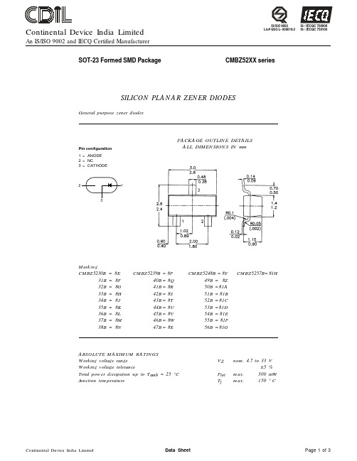
SILICON PLANAR ZENER DIODES General purpose zener diodesMarkingCMBZ5230B =8E CMBZ5239B = 8P CMBZ5248B = 8Y CMBZ5257B=81H31B =8F 40B =8Q 49B =8Z32B =8G 41B =8R 50B =81A33B =8H 42B =8S 51B =81B34B =8J 43B =8T 52B =81C35B =8K 44B =8U 53B =81D36B =8L 45B =8V 54B =81E37B =8M 46B =8W 55B =81F38B =8N 47B =8X 56B =81GABSOLUTE MAXIMUM RATINGSWorking voltage range V Z nom.4.7 to 33VWorking voltage tolerance ±5%Total power dissipation up to T amb = 25 °C P tot max.300mWJunction temperature T j max.150°CCMBZ52XX seriesPin configuration 1=ANODE2=NC3=CATHODEPACKAGE OUTLINE DETAILSALL DIMENSIONS IN m mIS / IECQC 700000IS / IECQC 750100IS/ISO 9002Lic# QSC/L- 000019.2Continental Device India LimitedAn IS/ISO 9002 and IECQ Certified ManufacturerCMBZ52XX series RATINGS (at T A = 25°C unless otherwise specified)Limiting valuesTotal power dissipation up to T amb = 25 °C*P tot max.300mW Total power dissipation up to T amb = 25 °C**P tot max.225mW Storage temperature T stg–55 to –150 °C Junction temperature T j max.150°C THERMAL RESISTANCEFrom junction to ambient R th j–a417°C/W From junction to ambient R th j–a556°C/W CHARACTERISTICST j = 25 °C unless otherwise specifiedV F = 0.9V Max. @ I F = 10 mADevice Zener Test Z ZK Z ZT Max@ V R Voltage Current I Z=0.25mA I Z = I ZT I R(V)V Z (± 5%)I ZT ohm max@10% Mod uANominal m A ohm max maxCMBZ-5230B 4.720190019 5.0 2.0 CMBZ-5231B 5.120160017 5.0 2.0 CMBZ-5232B 5.620160011 5.0 3.0 CMBZ-5233B 6.02016007.0 5.0 3.5 CMBZ-5234B 6.22010007.0 5.0 4.0 CMBZ-5235B 6.820750 5.0 3.0 5.0 CMBZ-5236B7.520500 6.0 3.0 6.0 CMBZ-5237B8.2205008.0 3.0 6.5 CMBZ-5238B8.7206008.0 3.0 6.5 CMBZ-5239B9.12060010 3.07.0 CMBZ-5240B102060017 3.08.0 CMBZ-5241B112060022 2.08.4 CMBZ-5242B122060030 1.09.1 CMBZ-5243B139.5600130.59.9 CMBZ-5244B149.0600150.110 CMBZ-5245B158.5600160.111 CMBZ-5246B167.8600170.112 CMBZ-5247B177.4600190.113 CMBZ-5248B187.0600210.114 CMBZ-5249B19 6.6600230.114 CMBZ-5250B20 6.2600250.115 CMBZ-5251B22 5.6600290.117* Device mounted on a ceramic alumina of 8 mm × 10 mm × 0.7 mm** Device mounted on an FR5 printed circuit boardCMBZ52XX seriesDevice Zener Test Z ZK Z ZT Max@ V RVoltage Current I Z=0.25mA I Z = I ZT I R(V)V Z (± 5%)I ZT ohm max@10% Mod uANominal m A ohm max maxCMBZ-5252B24 5.2600330.118CMBZ-5253B25 5.0600350.119CMBZ-5254B27 4.6600410.121CMBZ-5255B28 4.5600440.121CMBZ-5256B30 4.2600490.123CMBZ-5257B33 3.8700580.125DisclaimerThe product information and the selection guides facilitate selection of the CDIL's Discrete Semiconductor Device(s) best suited for application in your product(s) as per your requirement. It is recommended that you completely review our Data Sheet(s) so as to confirm that the Device(s) meet functionality parameters for your application. The information furnished on the CDIL Web Site/ CD is believed to be accurate and reliable. CDIL however, does not assume responsibility for inaccuracies or incomplete information. Furthermore, CDIL does not assume liability whatsoever, arising out of the application or use of any CDIL product; neither does it convey any license under its patent rights nor rights of others. These products are not designed for use in life saving/support appliances or systems. CDIL customers selling these products (either as individual Discrete Semiconductor Devices or incorporated in their end products), in any life saving/support appliances or systems or applications do so at their own risk and CDIL will not be responsible for any damages resulting from such sale(s).CDIL strives for continuous improvement and reserves the right to change the specifications of its products without prior notice.CDIL is a registered Trademark ofContinental Device India LimitedC-120 Naraina Industrial Area, New Delhi 110 028, India.Telephone + 91-11-579 6150 Fax + 91-11-579 9569, 579 5290e-mail sales@ 。
MMSZ5232BT1中文资料
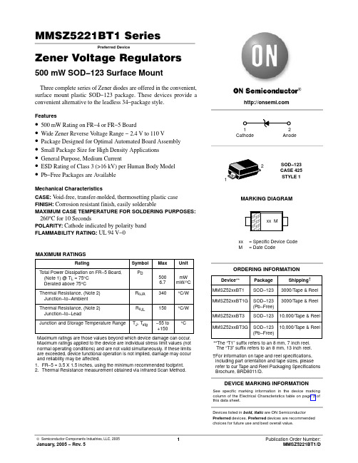
MMSZ5221BT1 SeriesPreferred DeviceZener Voltage Regulators 500 mW SOD−123 Surface MountThree complete series of Zener diodes are offered in the convenient, surface mount plastic SOD−123 package. These devices provide a convenient alternative to the leadless 34−package style.Features•500 mW Rating on FR−4 or FR−5 Board•Wide Zener Reverse V oltage Range − 2.4 V to 110 V •Package Designed for Optimal Automated Board Assembly •Small Package Size for High Density Applications •General Purpose, Medium Current•ESD Rating of Class 3 (>16 kV) per Human Body Model•Pb−Free Packages are AvailableMechanical CharacteristicsCASE:V oid-free, transfer-molded, thermosetting plastic case FINISH:Corrosion resistant finish, easily solderableMAXIMUM CASE TEMPERATURE FOR SOLDERING PURPOSES: 260°C for 10 SecondsPOLARITY:Cathode indicated by polarity band FLAMMABILITY RATING:UL 94 V−0MAXIMUM RATINGSMaximum ratings are those values beyond which device damage can occur. Maximum ratings applied to the device are individual stress limit values (not normal operating conditions) and are not valid simultaneously. If these limits are exceeded, device functional operation is not implied, damage may occur and reliability may be affected.1.FR−5 = 3.5 X 1.5 inches, using the minimum recommended footprint.2.Thermal Resistance measurement obtained via infrared Scan Method.See specific marking information in the device marking column of the Electrical Characteristics table on page 3 of this data sheet.DEVICE MARKING INFORMATIONDevices listed in bold, italic are ON Semiconductor Preferred devices. Preferred devices are recommended choices for future use and best overall value.ELECTRICAL CHARACTERISTICS (T A = 25°C unlessotherwise noted, V= 0.95 V Max. @ I = 10 mA)4.Nominal Zener voltage is measured with the device junction in thermal equilibrium at T L = 30°C $1°C.5.Z ZT and Z ZK are measured by dividing the AC voltage drop across the device by the ac current applied.The specified limits are for I Z(AC) = 0.1 I Z(dc) with the AC frequency = 1 KHz.V Z , NOMINAL ZENER VOLTAGE (V)−1012345678Figure 1. Temperature Coefficients (Temperature Range −55°C to +150°C)100101V Z , NOMINAL ZENER VOLTAGE (V)Figure 2. Temperature Coefficients (Temperature Range −55°C to +150°C)1.21.00.80.60.40.20T, TEMPERATURE (°C)Figure 3. Steady State Power Derating PW, PULSE WIDTH (ms)Figure 4. Maximum Nonrepetitive Surge Power1000100101V Z , NOMINAL ZENER VOLTAGEFigure 5. Effect of Zener Voltage onZener Impedance100101V F , FORWARD VOLTAGE (V)Figure 6. Typical Forward Voltage1000100101q V Z , T E M P E R A T U R E C O E F F I C I E N T (m V /°C )q V Z , T E M P E R A T U R E C O E F F I C I E N T (m V /°C )P p k , P E A K S U R G E P O W E R (W A T T S )Z Z T , D Y N A M I C I M P E D A N C E (W )I F , F O R W A R D C U R R E N T (m A )C , C A P A C I T A N C E (p F )V Z , NOMINAL ZENER VOLTAGE (V)Figure 7. Typical Capacitance 1000100101V Z , ZENER VOLTAGE (V)1001010.10.01V Z , ZENER VOLTAGE (V)1001010.10.01V Z , NOMINAL ZENER VOLTAGE (V)Figure 8. Typical Leakage CurrentFigure 9. Zener Voltage versus Zener Current(V Z Up to 12 V)Figure 10. Zener Voltage versus Zener Current(12 V to 91 V)I R , L E A K A G E C U R R E N T (m A )I Z , Z E N E R C U R R E N T (m A )I Z , Z E N E R C U R R E N T (m A )PACKAGE DIMENSIONSSOD−123CASE 425−04ISSUE Cǒmm inchesǓSCALE 10:1*For additional information on our Pb−Free strategy and solderingdetails, please download the ON Semiconductor Soldering and Mounting Techniques Reference Manual, SOLDERRM/D.SOLDERING FOOTPRINT*ON Semiconductor and are registered trademarks of Semiconductor Components Industries, LLC (SCILLC). SCILLC reserves the right to make changes without further notice to any products herein. SCILLC makes no warranty, representation or guarantee regarding the suitability of its products for any particular purpose, nor does SCILLC assume any liability arising out of the application or use of any product or circuit, and specifically disclaims any and all liability, including without limitation special, consequential or incidental damages.“Typical” parameters which may be provided in SCILLC data sheets and/or specifications can and do vary in different applications and actual performance may vary over time. All operating parameters, including “Typicals” must be validated for each customer application by customer’s technical experts. SCILLC does not convey any license under its patent rights nor the rights of others. SCILLC products are not designed, intended, or authorized for use as components in systems intended for surgical implant into the body, or other applications intended to support or sustain life, or for any other application in which the failure of the SCILLC product could create a situation where personal injury or death may occur. Should Buyer purchase or use SCILLC products for any such unintended or unauthorized application, Buyer shall indemnify and hold SCILLC and its officers, employees, subsidiaries, affiliates,and distributors harmless against all claims, costs, damages, and expenses, and reasonable attorney fees arising out of, directly or indirectly, any claim of personal injury or death associated with such unintended or unauthorized use, even if such claim alleges that SCILLC was negligent regarding the design or manufacture of the part. SCILLC is an Equal Opportunity/Affirmative Action Employer. This literature is subject to all applicable copyright laws and is not for resale in any manner.PUBLICATION ORDERING INFORMATION。
CMKZ5232B中文资料
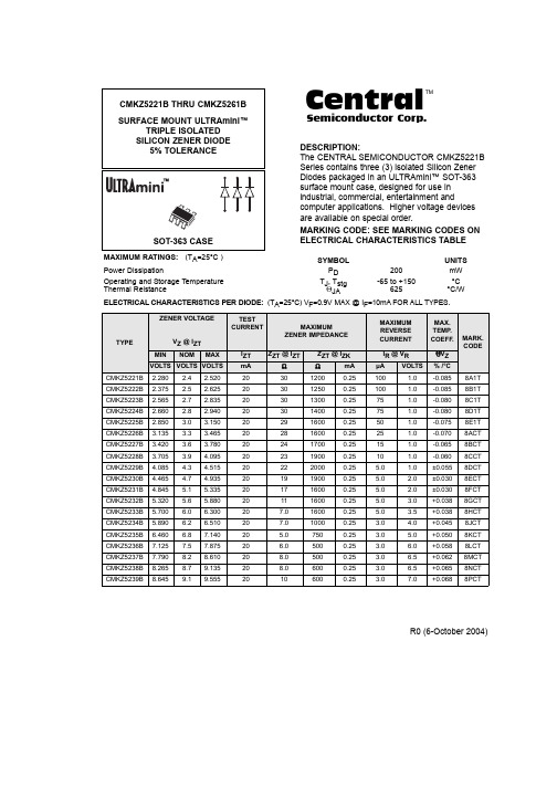
CMKZ5221B THRU CMKZ5261B SURFACE MOUNT ULTRAmini™ TRIPLE ISOLATED SILICON ZENER DIODE 5% TOLERANCE
Central
TM
Semiconductor Corp.
DESCRIPTION: The CENTRAL SEMICONDUCTOR CMKZ5221B Series contains three (3) isolated Silicon Zener Diodes packaged in an ULTRAmini™ SOT-363 surface mount case, designed for use in industrial, commercial, entertainment and computer applications. Higher voltage devices are available on special order. MARKING CODE: SEE MARKING CODES ON ELECTRICAL CHARACTERISTICS TABLE
ZENER VOLTAGE VZ @ IZT MIN CMKZ5221B CMKZ5222B CMKZ5223B CMKZ5224B CMKZ5225B CMKZ5226B CMKZ5227B CMKZ5228B CMKZ5229B CMKZ5230B CMKZ5231B CMKZ5232B CMKZ5233B CMKZ5234B CMKZ5235B CMKZ5236B CMKZ5237B CMKZ5238B CMKZ5239B 2.280 2.375 2.565 2.660 2.850 3.135 3.420 3.705 4.085 4.465 4.845 5.320 5.700 5.890 6.460 7.125 7.790 8.265 8.645 NOM 2.4 2.5 2.7 2.8 3.0 3.3 3.6 3.9 4.3 4.7 5.1 5.6 6.0 6.2 6.8 7.5 8.2 8.7 9.1 MAX 2.520 2.625 2.835 2.940 3.150 3.465 3.780 4.095 4.515 4.935 5.335 5.880 6.300 6.510 7.140 7.875 8.610 9.135 9.555 IZT mA 20 20 20 20 20 20 20 20 20 20 20 20 20 20 20 20 20 20 20 VOLTS VOLTS VOLTS TEST CURRENT MAXIMUM ZENER IMPEDANCE ZZT @ IZT Ω 30 30 30 30 29 28 24 23 22 19 17 11 7.0 7.0 5.0 6.0 8.0 8.0 10 ZZT @ IZK Ω 1200 1250 1300 1400 1600 1600 1700 1900 2000 1900 1600 1600 1600 1000 750 500 500 600 600 mA 0.25 0.25 0.25 0.25 0.25 0.25 0.25 0.25 0.25 0.25 0.25 0.25 0.25 0.25 0.25 0.25 0.25 0.25 0.25 MAXIMUM REVERSE CURRENT IR @ VR µA 100 100 75 75 50 25 15 10 5.0 5.0 5.0 5.0 5.0 3.0 3.0 3.0 3.0 3.0 3.0 VOLTS 1.0 1.0 1.0 1.0 1.0 1.0 1.0 1.0 1.0 2.0 2.0 3.0 3.5 4.0 5.0 6.0 6.5 6.5 7.0 MAX. TEMP. COEFF. ΘVZ % /°C -0.085 -0.085 -0.080 -0.080 -0.075 -0.070 -0.065 -0.060 ±0.055 ±0.030 ±0.030 +0.038 +0.038 +0.045 +0.050 +0.058 +0.062 +0.065 +0.068 8A1T 8B1T 8C1T 8D1T 8E1T 8ACT 8BCT 8CCT 8DCT 8ECT 8FCT 8GCT 8HCT 8JCT 8KCT 8LCT 8MCT 8NCT 8PCT
195-2011 中国联通M2M UICC卡技术规范V2.0
MMSZ5230中文资料
1/20/99
元器件交易网
MMSZ5225 THRU MMSZ5267
ELECTRICAL CHARACTERISTICS
Ratings at 25°C ambient temperature unless otherwise specified.
Type
Marking Code
-0.075 -0.070 -0.065 -0.060 -0.055 ±0.030 ±0.030 +0.038 +0.038 +0.045 +0.050 +0.058 +0.062 +0.065 +0.068 +0.075 +0.076 +0.077 +0.079 +0.082 +0.082 +0.083 +0.084 +0.085 +0.086 +0.086 +0.087 +0.087 +0.089 +0.090 +0.091 +0.091 +0.092 +0.093 +0.094 +0.095 +0.095 +0.096 +0.096 +0.097 +0.097 +0.097 +0.098
1.0 1.0 1.0 1.0 1.0 2.0 2.0 3.0 3.5 4.0 5.0 6.0 6.5 6.5 7.0 8.0 8.4 9.1 9.9 10 11 12 13 14 14 15 17 18 19 21 21 23 25 27 30 33 36 39 43 46 47 52 56
NOTES: (1) The Zener Impedance is derived from the 1kHz AC voltage which results when an AC current having an RMS value equal to 10% of the Zener current (IZT or IZK) is superimposed on IZT or IZK. Zener Impedance is measured at two points to insure a sharp knee on the breakdown curve and to eliminate unstable units. (2) Measured with device junction in thermal equilibrium.
ZMM5252B中文资料(WILLAS ELECTRONIC)中文数据手册「EasyDatasheet - 矽搜」
5264
ZMM5265B
62.0
58.90
65.10
185
2.0
1400
0.25
0.1
47.0
5265
ZMM5266B
68.0
64.60
71.40
230
1.8
1600
0.25
0.1
52.0
5266
ZMM5267B
75.0
71.25
78.75
270
1.7
1700
0.25
0.1
56.0
5267
1)基于直流测量达到热平衡;引线长度=9.5毫米(3/8");散热器= 30K / W热阻
5244
ZMM5245B
15.0
14.25
15.75
16
8.5
600
0.25
0.1
11.0
5245
ZMM5246B
16.0
15.20
16.80
17
7.8
600
0.25
0.1
12.0
5246
ZMM5247B
17.0
16.15
17.85
19
7.4
600
0.25
0.1
13.0
5247
ZMM5248B
18.0
类型
max. .006 (0.15)
符号
PTOT IZ Tj Tstg
值
500
PV/V Z -65到+175 –65 至 +175
单元
mW
mA °C °C
.010 (0.25) min.
Marking Code: 测JV o试r 4条件
TZQ5230B中文资料

1.)Based on dc measurement at thermal equilibrium; case temperature maintained at 30°C ± 2°C.
www.vishay.de • FaxBack +1-408-970-5600 2 (6)
Document Number 85612 Rev. 3, 01-Apr-99
元器件交易网
TZQ5221B...TZQ5267B
Vishay Telefunken
Silicon Epitaxial Planar Z–Diodes
Features
D D D D D
Very sharp reverse characteristic Low reverse current level Available with tighter tolerances Very high stability Low noise
W
mA
< 100 < 100 < 75 < 75 < 50 < 25 < 15 < 10 <5 <5 <5 <5 <5 <5 <3 <3 <3 <3 <3 <3 <2 <1 < 0.5 < 0.1 < 0.1 < 0.1 < 0.1 < 0.1 < 0.1 < 0.1 < 0.1 < 0.1 < 0.1 < 0.1 < 0.1 < 0.1 < 0.1 < 0.1 < 0.1 < 0.1 < 0.1 < 0.1 < 0.1 < 0.1 < 0.1 < 0.1 < 0.1
金智科技 WDZ-5232 电动机保护测控装置 说明书

保护动作判据
零序过流:
I 0 I 02 dz t0 t02 dz
相电流制动:
I 0 I 02 dz I 0 1 I max I e 1.05 4I 02 dz t t 0 02 dz
I max 1.05 I e I max 1.05 I e
第 6 页 共 29 页
WDZ-5232 电动机保护测控装置(V1.07)
2.9
堵转保护 装置利用转速开关接点和过流元件构成堵转保护。转速开关需要在开入中进行关联。
2.9.1
保护动作逻辑框图
2.9.2
保护动作判据
I max I dz t t dz 转速开关闭合
式中,Idz:堵转保护动作电流整定值(A) tdz:堵转保护动作时间整定值(s) 2.10 长起动保护 电动机起动过程中,如果时间过长,会严重影响电动机的安全运行。装置提供长起动保 护,对电动机的起动过程进行保护。 电动机的正常额定起动过程中出现的最大起动电流为额定起动电流 Iqde,在此情况下电 动机允许的堵转时间为 tyd。电动机起动过程中,起动电流越大,则相应的允许起动时间应 该越短,否则应该越长。使用以下公式计算电动机起动过程中的允许起动时间。
3 I 1 I a I b e j 240 I c e j120
二电流互感器方式,正序电流的计算公式为:
j 3 I 1 I a e j 60 I c
2.11.2 保护动作逻辑框图
Trip
&
Signal Warn
2.11.3 保护动作判据
Trip
≥1
Signal Warn
HMBZ5222B中文资料
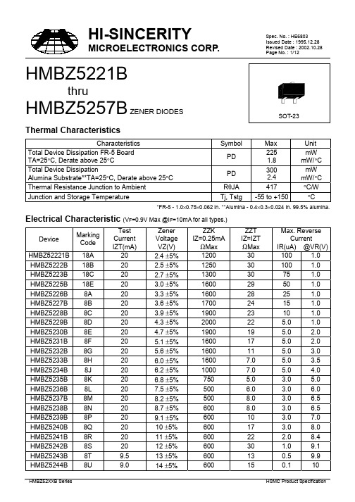
Page No. : 1/12 HMBZ5221BthruHMBZ5257B ZENER DIODESThermal CharacteristicsCharacteristics Symbol Max UnitTotal Device Dissipation FR-5 Board TA=25°C, Derate above 25°C PD2251.8mWmW/°CTotal Device DissipationAlumina Substrate**TA=25°C, Derate above 25°C PD3002.4mWmW/°CThermal Resistance Junction to Ambient RθJA417°C/W Junction and Storage Temperature Tj, Tstg-55 to +150°C*FR-5 - 1.0×0.75×0.062 in. **Alumina - 0.4×0.3×0.024 in. 99.5% alumina. Electrical Characteristic (V F=0.9V Max @I F=10mA for all types.)Test CurrentZenerVoltageZZKIZ=0.25mAZZTIZ=IZTMax. ReverseCurrentDevice MarkingCodeIZT(mA)VZ(V)ΩMaxΩMax IR(uA)@VR(V)HMBZ52221B18A20 2.4 ±5%120030100 1.0 HMBZ5222B18B20 2.5 ±5%125030100 1.0 HMBZ5223B18C20 2.7 ±5%13003075 1.0 HMBZ5225B18E20 3.0 ±5%16002950 1.0 HMBZ5226B8A20 3.3 ±5%16002825 1.0 HMBZ5227B8B20 3.6 ±5%17002415 1.0 HMBZ5228B8C20 3.9 ±5%19002310 1.0 HMBZ5229B8D20 4.3 ±5%200022 5.0 1.0 HMBZ5230B8E20 4.7 ±5%190019 5.0 2.0 HMBZ5231B8F20 5.1 ±5%160017 5.0 2.0 HMBZ5232B8G20 5.6 ±5%160011 5.0 3.0 HMBZ5233B8H20 6.0 ±5%16007.0 5.0 3.5 HMBZ5234B8J20 6.2 ±5%10007.0 5.0 4.0 HMBZ5235B8K20 6.8 ±5%750 5.0 3.0 5.0 HMBZ5236B8L207.5 ±5%500 6.0 3.0 6.0 HMBZ5237B8M208.2 ±5%5008.0 3.0 6.5 HMBZ5238B8N208.7 ±5%6008.0 3.0 6.5 HMBZ5239B8P209.1 ±5%60010 3.07.0 HMBZ5240B8Q2010 ±5%60017 3.08.0 HMBZ5241B8R2011 ±5%60022 2.08.4 HMBZ5242B8S2012 ±5%60030 1.09.1Page No. : 2/12HMBZ5245B 8V 8.515 ±5%600160.111HMBZ5246B 8W 7.816 ±5%600170.112HMBZ5247B 8X 7.417±5%600190.113HMBZ5248B 8Y 7.018 ±5%600210.114HMBZ5249B 8Z 6.619 ±5%600230.114HMBZ5250B 81A 6.220 ±5%600250.115HMBZ5251B 81B 5.622 ±5%600290.117HMBZ5252B 81C 5.224 ±5%600330.118HMBZ5253B 81D 5.025 ±5%600350.119HMBZ5254B 81E 4.627 ±5%600410.121HMBZ5255B 81F4.528 ±5%600440.121HMBZ5256B 81G 4.230 ±5%600490.123HMBZ5257B81H3.833 ±5%700580.125Characteristics CurvePage No. : 3/12Page No. : 8/12Page No. : 11/12Page No. : 12/12SOT-23 Dimension*: TypicalInches MillimetersInches MillimetersDIM Min.Max.Min.Max.DIM Min.Max.Min.Max.A 0.11020.1204 2.80 3.04J0.00340.00700.0850.177B 0.04720.0630 1.20 1.60K 0.01280.02660.320.67C 0.03350.05120.89 1.30L 0.03350.04530.85 1.15D0.01180.01970.300.50S 0.08300.1083 2.10 2.75G 0.06690.0910 1.70 2.30V0.00980.02560.250.65H0.00050.00400.0130.10Notes: 1.Dimension and tolerance based on our Spec. dated Sep. 07,1997.2.Controlling dimension: millimeters.3.Maximum lead thickness includes lead finish thickness, and minimum lead thickness is the minimum thickness of base material.4.If there is any question with packing specification or packing method, please contact your local HSMC sales office.Material:• Lead: 42 Alloy; solder plating• Mold Compound: Epoxy resin family, flammability solid burning class: UL94V-0Important Notice:• All rights are reserved. Reproduction in whole or in part is prohibited without the prior written approval of HSMC.• HSMC reserves the right to make changes to its products without notice.• HSMC semiconductor products are not warranted to be suitable for use in Life-Support Applications, or systems.• HSMC assumes no liability for any consequence of customer product design, infringement of patents, or application assistance.Head Office And Factory:• Head Office (Hi-Sincerity Microelectronics Corp.): 10F.,No. 61, Sec. 2, Chung-Shan N. Rd. Taipei Taiwan R.O.C.Tel: 886-2-25212056 Fax: 886-2-25632712, 25368454• Factory 1: No. 38, Kuang Fu S. Rd., Fu-Kou Hsin-Chu Industrial Park Hsin-Chu Taiwan. R.O.C Tel: 886-3-5983621~5 Fax: 886-3-5982931。
MMSZ5233中文资料

NEW PRODUCT
NEW PRODUCT
MMSZ5225 THRU MMSZ5267
ZENER DIODES
SOD-123
.022 (0.55)
FEATURES
♦ Silicon Planar Power Zener Diodes ♦ Standard Zener voltage tolerance is ± 5% with a “B” suffix. Other tolerances are available upon request. ♦ These diodes are also available in Mini-MELF case with the designation ZMM5225 ... ZMM5267, DO-35 case with type designation 1N5225 ... 1N5267 and SOT-23 case with the type designation MMBZ5225 ... MMBZ5267.
MECHANICAL DATA
Case: SOD-123 Plastic Case Weight: approx. 0.01 g
Dimensions in inches and (millimeters)
MAXIMUM RATINGS AND ELECTRICAL CHARACTERISTICS
Ratings at 25°C ambient temperature unless otherwise specified.
-0.075 -0.070 -0.065 -0.060 -0.055 ±0.030 ±0.030 +0.038 +0.038 +0.045 +0.050 +0.058 +0.062 +0.065 +0.068 +0.075 +0.076 +0.077 +0.079 +0.082 +0.082 +0.083 +0.084 +0.085 +0.086 +0.086 +0.087 +0.087 +0.089 +0.090 +0.091 +0.091 +0.092 +0.093 +0.094 +0.095 +0.095 +0.096 +0.096 +0.097 +0.097 +0.097 +0.098
MMBZ5242B贴片二极管规格书

50
1.0
25
1.0
15
1.0
10
1.0
5.0
1.0
5.0
2.0
5.0
2.0
5.0
3.0
5.0
3.5
5.0
4.0
3.0
5.0
3.0
6.0
3.0
6.5
3.0
6.5
3.0
7.0
3.0
8.0
2.0
8.4
1.0
9.1
0.5
9.9
0.1
10
0.1
11
0.1
12
0.1
13
0.1
14
0.1
14
0.1
15
0.1
17
VZ @ IZT
Min (V) 2.28 2.38 2.57 2.85 3.14 3.42 3.71 4.09 4.47 4.85 5.32 5.70 5.89 6.46 7.13 7.79 8.27 8.65 9.50 10.45 11.40 12.35 13.30 14.25 15.20 16.15 17.10 18.05 19.00 20.90 22.80 23.75 25.65 26.60 28.50 31.35 34.20 37.05
ELECTRICAL CHARACTERISTICS (Ta=25℃ unless otherwise specified)
Type Number
MMBZ5221B MMBZ5222B MMBZ5223B MMBZ5225B MMBZ5226B MMBZ5227B MMBZ5228B MMBZ5229B MMBZ5230B MMBZ5231B MMBZ5232B MMBZ5233B MMBZ5234B MMBZ5235B MMBZ5236B MMBZ5237B MMBZ5238B MMBZ5239B MMBZ5240B MMBZ5241B MMBZ5242B MMBZ5243B MMBZ5244B MMBZ5245B MMBZ5246B MMBZ5247B MMBZ5248B MMBZ5249B MMBZ5250B MMBZ5251B MMBZ5252B MMBZ5253B MMBZ5254B MMBZ5255B MMBZ5256B MMBZ5257B MMBZ5258B MMBZ5259B
- 1、下载文档前请自行甄别文档内容的完整性,平台不提供额外的编辑、内容补充、找答案等附加服务。
- 2、"仅部分预览"的文档,不可在线预览部分如存在完整性等问题,可反馈申请退款(可完整预览的文档不适用该条件!)。
- 3、如文档侵犯您的权益,请联系客服反馈,我们会尽快为您处理(人工客服工作时间:9:00-18:30)。
SILICON PLANAR ZENER DIODES General purpose zener diodes
Marking
CMBZ5230B =8E CMBZ5239B = 8P CMBZ5248B = 8Y CMBZ5257B=81H
31B =8F 40B =8Q 49B =8Z
32B =8G 41B =8R 50B =81A
33B =8H 42B =8S 51B =81B
34B =8J 43B =8T 52B =81C
35B =8K 44B =8U 53B =81D
36B =8L 45B =8V 54B =81E
37B =8M 46B =8W 55B =81F
38B =8N 47B =8X 56B =81G
ABSOLUTE MAXIMUM RATINGS
Working voltage range V Z nom.4.7 to 33V
Working voltage tolerance ±5%
Total power dissipation up to T amb = 25 °C P tot max.300mW
Junction temperature T j max.150°C
CMBZ52XX series
Pin configuration 1=ANODE
2=NC
3=CATHODE
PACKAGE OUTLINE DETAILS
ALL DIMENSIONS IN m m
IS / IECQC 700000
IS / IECQC 750100IS/ISO 9002
Lic# QSC/L- 000019.2Continental Device India Limited
An IS/ISO 9002 and IECQ Certified Manufacturer
CMBZ52XX series RATINGS (at T A = 25°C unless otherwise specified)
Limiting values
Total power dissipation up to T amb = 25 °C*P tot max.300mW Total power dissipation up to T amb = 25 °C**P tot max.225mW Storage temperature T stg–55 to –150 °C Junction temperature T j max.150°C THERMAL RESISTANCE
From junction to ambient R th j–a417°C/W From junction to ambient R th j–a556°C/W CHARACTERISTICS
T j = 25 °C unless otherwise specified
V F = 0.9V Max. @ I F = 10 mA
Device Zener Test Z ZK Z ZT Max@ V R Voltage Current I Z=0.25mA I Z = I ZT I R(V)
V Z (± 5%)I ZT ohm max@10% Mod uA
Nominal m A ohm max max
CMBZ-5230B 4.720190019 5.0 2.0 CMBZ-5231B 5.120160017 5.0 2.0 CMBZ-5232B 5.620160011 5.0 3.0 CMBZ-5233B 6.02016007.0 5.0 3.5 CMBZ-5234B 6.22010007.0 5.0 4.0 CMBZ-5235B 6.820750 5.0 3.0 5.0 CMBZ-5236B7.520500 6.0 3.0 6.0 CMBZ-5237B8.2205008.0 3.0 6.5 CMBZ-5238B8.7206008.0 3.0 6.5 CMBZ-5239B9.12060010 3.07.0 CMBZ-5240B102060017 3.08.0 CMBZ-5241B112060022 2.08.4 CMBZ-5242B122060030 1.09.1 CMBZ-5243B139.5600130.59.9 CMBZ-5244B149.0600150.110 CMBZ-5245B158.5600160.111 CMBZ-5246B167.8600170.112 CMBZ-5247B177.4600190.113 CMBZ-5248B187.0600210.114 CMBZ-5249B19 6.6600230.114 CMBZ-5250B20 6.2600250.115 CMBZ-5251B22 5.6600290.117
* Device mounted on a ceramic alumina of 8 mm × 10 mm × 0.7 mm
** Device mounted on an FR5 printed circuit board
CMBZ52XX series
Device Zener Test Z ZK Z ZT Max@ V R
Voltage Current I Z=0.25mA I Z = I ZT I R(V)
V Z (± 5%)I ZT ohm max@10% Mod uA
Nominal m A ohm max max
CMBZ-5252B24 5.2600330.118
CMBZ-5253B25 5.0600350.119
CMBZ-5254B27 4.6600410.121
CMBZ-5255B28 4.5600440.121
CMBZ-5256B30 4.2600490.123
CMBZ-5257B33 3.8700580.125
Disclaimer
The product information and the selection guides facilitate selection of the CDIL's Discrete Semiconductor Device(s) best suited for application in your product(s) as per your requirement. It is recommended that you completely review our Data Sheet(s) so as to confirm that the Device(s) meet functionality parameters for your application. The information furnished on the CDIL Web Site/ CD is believed to be accurate and reliable. CDIL however, does not assume responsibility for inaccuracies or incomplete information. Furthermore, CDIL does not assume liability whatsoever, arising out of the application or use of any CDIL product; neither does it convey any license under its patent rights nor rights of others. These products are not designed for use in life saving/support appliances or systems. CDIL customers selling these products (either as individual Discrete Semiconductor Devices or incorporated in their end products), in any life saving/support appliances or systems or applications do so at their own risk and CDIL will not be responsible for any damages resulting from such sale(s).
CDIL strives for continuous improvement and reserves the right to change the specifications of its products without prior notice.
CDIL is a registered Trademark of
Continental Device India Limited
C-120 Naraina Industrial Area, New Delhi 110 028, India.
Telephone + 91-11-579 6150 Fax + 91-11-579 9569, 579 5290
e-mail sales@ 。
