RDXA-R858-T813A中文资料
R1288A中文资料

For High Temperature Scintillation Counting,Ruggedized, Low Profile, 25 mm (1 Inch) Diameter,High Temp. Bialkali Photocathode, 10-stage, Head-on TypeSupply Voltage: 1500 V , K: Cathode, Dy: Dynode, P: AnodeShock............10 000 m/s 2, 0.5 ms, 3 impact shocks per direction (6 directions)Vibration........300 m/s 2, 50 Hz to 2000 Hz, 1 oct per minute, 3 sweeps per axis (3 axes)STANDARD VOLTAGE DIVIDER AND SUPPLY VOLTAGEENVIRONMENTAL TESTINGElectrodes Ratio K Dy13Dy21Dy31Dy41Dy51Dy61Dy711Dy8Dy9Dy10P 111NOTE: Anode characteristics are measured with a voltage distribution ratio shown belowsubject to change without notice. No patent rights are granted to any of the circuits described herein. ©2003 Hamamatsu Photonics K.K.Subject to local technical requirements and regulations, availability of products included in this promotional material may vary. Please consult with our sales office.Figure 1: Typical Spectral ResponseTPMH1279E01MAR. 2003 IPTPMHB0061EAFigure 2: Typical Gain CharacteristicsTPMHB0693EAFigure 3: Dimensional Outline and Basing Diagram (Unit: mm)TPMHA0363EBTACCA0009EBSocket E678-12A(Supplied)10-1102100101WAVELENGTH (nm)C A T H O D E R A D I A N T S E N S I T I V I T Y (m A /W )Q U A N T U M E F F I C I E N C Y (%)A Temporary Base Removed DY3DY6HAMAMATSU PHOTONICS K.K., Electron Tube Center314-5, Shimokanzo, Toyooka-village, Iwata-gun, Shizuoka-ken, 438-0193, Japan, Telephone: (81)539/62-5248, Fax: (81)539/62-2205U.S.A.: Hamamatsu Corporation: 360 Foothill Road, P. O. Box 6910, Bridgewater. N.J. 08807-0910, U.S.A., Telephone: (1)908-231-0960, Fax: (1)908-231-1218 E-mail: usa@Germany: Hamamatsu Photonics Deutschland GmbH: Arzbergerstr. 10, D-82211 Herrsching am Ammersee, Germany, Telephone: (49)8152-375-0, Fax: (49)8152-2658 E-mail: info@hamamatsu.deFrance: Hamamatsu Photonics France S.A.R.L.: 8, Rue du Saule Trapu, Parc du Moulin de Massy, 91882 Massy Cedex, France, Telephone: (33)1 69 53 71 00, Fax: (33)1 69 53 71 10 E-mail: infos@hamamatsu.frUnited Kingdom: Hamamatsu Photonics UK Limited: 2 Howard Court, 10 Tewin Road Welwyn Garden City Hertfordshire AL7 1BW, United Kingdom, Telephone: 44-(0)1707-294888, Fax: 44(0)1707-325777 E-mail: info@ North Europe: Hamamatsu Photonics Norden AB: Smidesv ägen 12, SE-171-41 SOLNA, Sweden, Telephone: (46)8-509-031-00, Fax: (46)8-509-031-01 E-mail: info@hamamatsu.seItaly: Hamamatsu Photonics Italia: S.R.L.: Strada della Moia, 1/E, 20020 Arese, (Milano), Italy, Telephone: (39)02-935 81 733, Fax: (39)02-935 81 741 E-mail: info@hamamatsu.itWEB SITE 500700100015002000at 25°CSUPPLY VOLTAGE (V)G A I N107106105104103102108。
AD8138ARZ中文资料

PCF8583中文资料_带有 256×8bit RAM 的 8 引脚日历时钟芯片

PCF8583中文资料 芯片简介:1、PCF8583是P H IL IPS公司制造的带有256×8bit RAM的8引脚日历/时钟芯片,采用I2C2、两线串行总线接口,内含完整的振荡,分频,上电复位电路,并具备计时,日历,定时,闹钟和中断输出功能.3、日历/时钟芯片I2C总线RAM定时器4、带256字节RAM的实时时钟芯片PCF85831.芯片特点●数据保持和时钟工作电压1~6V ,总线工作电压2. 5~6V ;●采用8脚D IP或SO封装形式;●I2C两线串行总线接口;●内含256×8bit静态RAM ;●有定时,定闹功能和中断输出;●内有振荡器,分频器和上电复位电路,可使用32 768Hz石英晶振或外部50Hz时钟;●片内字节地址读写后自动加一;●可用作定时器或计数器.2.引脚功能PCF8583引脚功能如图1所列.芯片结构图1:3.片内寄存器功能描述在256字节RAM中,前16字节(地址00~0F H)是带有特殊功能的寄存器,现分述如下:内部结构如图2:3. 1状态寄存器(地址00H)状态寄存器控制着芯片所有的功能和操作,其内容如图3所列.图3 PCF8583状态寄存器详细说明如下:00寄存器(状态寄存器)8个位名称功能:0、计时器计时器到标志1闹钟定闹时间到标志查询IC价格,上IC酷搜网http://www.icqoso.com/data-PCF8583T.html 查询IC价格,上IC酷搜网http://www.icqoso.com/data-PCF8583T.html 查询IC价格,上IC酷搜网http://www.icqoso.com/data-PCF8583T.html 2闹钟使能(是否闹钟允许)0:禁止;1 :允许3屏蔽05和06字节屏蔽0 :不屏蔽;1 :屏蔽4~5功能模式芯片工作方式00:32768 Hz时钟;01 :50 Hz时钟;10 :计数器模式;11 :测试模式6计数锁存0:计数;1 :锁存7计数停止停止计数标志0:计数;1 :停止计数,分频器复位3. 2时钟计数器(地址01H~06H)查询IC价格,上IC酷搜网http://www.icqoso.com/data-PCF8583T.html 通过设置状态寄存器,可以选择32 768Hz和50Hz时钟模式或计数器模式.各时钟计数器功能如图4-7所列.1/ 100秒,秒,分,小时依次在地址01~04H.年以0~3表示,0为闰年.小时计数器的高2位分别作为12小时或24小时模式选择(0为24h , 1为12h)和上下午指示(0为AM ,1为PM).年份和日期,星期和月份分别在地址05H和06H.如果状态寄存器的屏蔽位有效,当读这些寄存器时,年份和星期的有关位会被屏蔽,这样允许用户直接读取日期和月份.在芯片以计数器方式工作时,计数器对振荡器输入端的脉冲计数,最多可达到6位数.以BCD码格式依次放在地址01~03H中,此时分频器无效.08寄存器(控制寄存器)8位使用说明:(2种模式,由00寄存器4-5位来控制)图8 时钟和日历计数器(时钟方式)地址bit7bit6bit5bit4~0011/ 100秒(0~99)02秒(0~59)03分(0~59)0424/ 12hAM/ PM 小时(0/ 1~24/ 12)05年(0~3)日期(1~28/ 29/ 30/ 31)06星期(0~6)月(1~12)07计时器(0~99)08闹钟控制寄存器09闹钟1/ 100秒0A 闹钟秒0B 闹钟分0C 闹钟小时0D 闹钟日期0E 闹钟月份查询IC价格,上IC酷搜网http://www.icqoso.com/data-PCF8583T.html 查询IC价格,上IC酷搜网http://www.icqoso.com/data-PCF8583T.html 0F闹钟计时器在设置时间时,应设置状态寄存器的停止位停止时钟,否则可能导致时钟混乱.3. 3计时器(地址07H)设置状态寄存器为XX0XX1XX可以打开计时器.在时钟模式中,计时器可以编程为以1/ 100秒,秒,分,小时或天计数.缺省状态下,计时器按天数累计.计时器为百进计数,溢出时,timer标志被置位,这个标志必须由软件来复位,通过设置闹钟寄存器的计时器中断允许位,可以传递到IN T脚引起中断.计时器的分辨率可通过设置定闹寄存器的低3位来编程(如表4所列).3. 4闹钟控制寄存器(地址08H)闹钟控制寄存器是用来控制定闹,定时和中断输出功能的.在时钟和计数器方式下有不同的功能(如表4所列).3. 5闹钟寄存器(地址09H~0F H)设置状态寄存器可以激活闹钟寄存器.设置闹钟控制寄存器可以选择定闹方式,闹钟时间到会使状态寄存器中的alarm标志置高,当alarm中断允许标志为1时,输出IN T引脚被拉低,并一直保持到复位或被软件清除.闹钟寄存器以时钟计数器相同的顺序放在地址09H以后的位置上(如表3所列),当闹钟寄存器每位都符合对应的时钟计数器时产生一个闹钟信号.通过设置闹钟计数器,闹钟可以被编程为控制日期,每天,每周或一段时间后启动;指定日期的闹钟忽略年和周位;日闹钟忽略月和日期位;周闹钟时,周/月寄存器将选择一周相应的一天启动闹钟,此时闹钟月份寄存器(0EH)改为星期寄存器,低七位对应周日到周六,最高位不用.另外,通过设置计时报警位,可以编程为定时闹钟.当计时器(0F H)值和时钟计数器(07H)位相同时,报警启动(alarm标志置1).在12小时模式时,第6和第7位的时寄存器一样.3. 6计数器的模式状态寄存器为XX10XXXX 时,可以选择计数器模式,计数器模式仅使用RAM 的01H~03H 字节,用于对O SC I 端脉冲的计数(O SCO 开路).计数器最大可计到百万(6位BCD 码).如允许计数报警,当计数器的值与09H,0A H,0B H 位的值相同时将发生一次计数报警, alarm 标志被置1 ,设置中断允许可引发中断.在此模式下,计时器(07H)受报警控制寄存器低3位控制,计时器的功能和时钟模式相同.4.芯片其它功能4. 1中断输出IN T 端图10 闹钟控制寄存器bit 名称时钟功能计数器功能0~2timer计时器设置000:无计时器001 :1/ 100秒查询IC价格,上IC酷搜网http://www.icqoso.com/data-PCF8583T.html 010 :秒011 :分100 :小时101 :日110 :不用111 :测试模式计时器设置000:无计时器001 :1010 :100011 :10000100 :1000000101 :禁止110 :禁止111 :测试模式3timer IN Tenable计时器中断允许0:禁止 1 :允许计时器中断允许0:禁止 1 :允许4~5alarm时钟定闹设置00:无闹钟01 :日期闹钟10 :周闹钟11 :每日闹钟定闹设置00:无定闹01 :定闹方式10 ,11 :禁止6timer alarm enable计时器报警允许 0:禁止 1 :允许计时器报警允许0:禁止 1 :允许7alarmIN Tenable报警中断允许0:禁止 1 :允许报警中断允许0:禁止 1 :允许与89c5252连接图,定时int输出控制cpu外部中断0 唤醒休眠中的cpu也可一唤醒掉电的cpu。
rtc8563
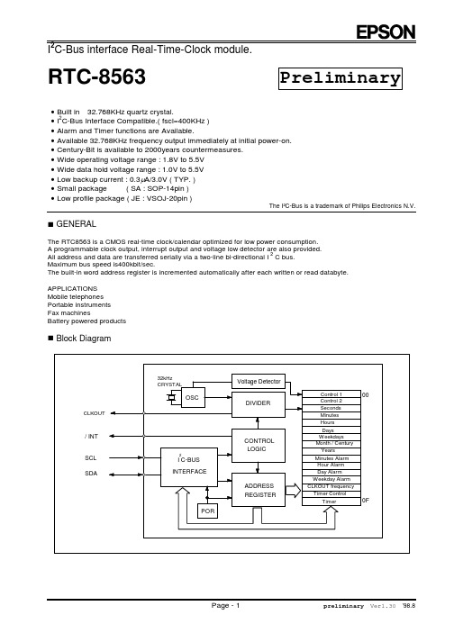
n Block Diagram
CLKOUT / INT SCL SDA
32kHz CRYSTAL
OSC
Voltage Detector DIVIDER
MIN.
TYP.
MAX.
Unit
IDDO
fSCL=400KHz fSCL=100KHz
800
mABiblioteka 200mAIDD fSCL=0Hz, VDD=5.0V
0.35
0.75
mA
fSCL=0Hz, VDD=3.0V
0.30
0.65
mA
fSCL=0Hz, VDD=2.0V
0.25
0.60
mA
IDD32K fSCL=0Hz, VDD=5.0V
bit 4
bit 3
bit 2
bit 1
bit 0
00
Control 1
TEST
0
STOP
0
TEST
0
0
0
01
Control 2
0
0
0
TI / TP
AF
TF
AIE
TIE
02
Seconds
VL
4
2
1
8
4
2
1
03
Minutes
x
4
2
1
8
4
2
1
04
Hours
x
x
2
1
8
东芝芯片资料
0 900Ω 600Ω 19.5K 15K 13K 19K
LA7833引脚功能
引脚
1 2 3 4 4 6 7
功能
接地端 场输出 自举升压电源端 场激励输入 负反馈输入及相位补偿 电源端 场逆程脉冲输出
直流电压
0V 13.6V 25.5V 0.8V 0.8V 26V 1.4V
纹波滤波电路引脚 第二伴音中频输出 调频直流反馈滤波电路引脚
电压
1.8V 0V 1.3V
+2.5V
+5V 2.45V 2.45V
1V 6.4V 0V 0V 2.3V 1.6V 0V +5V 3.6V 4.3V 0V 8V 8.8V 3.5V 5.6V 3.4V 3.5V
RXIK档对地电阻(黑表笔接地)
场AGC 总线时钟端子 总线数据端子
行电源 SECAM识别/载波信号输出
行逆程脉冲输入 复合同步信号输出 行激励信号输出
接地 沙堡脉冲输出 视频信号输出
数字电源
SECAM蓝色差信号输入 SECAM红色差信号输入
亮度信号输入 行AFC滤波
外接视频信号
接地 视频信Leabharlann 输入黑电平检测滤波直流电压(V)
有信号 4.9
800Ω 0
12.5K
12.8K
6K 13K 13K 13K 12.8K 13.2K
0 12.8K 13K 11.5K
1K 12.5K 12K
0 900Ω 600Ω 12.5K 12.2K 11.5K 12K
红笔接地 R×1K档
800Ω 0
19K
27K
5.5K 20K 20K 18K 28K 28K
R813系列中文说明书

R813
R813
R813
R813
R813
16 17 17
6.1最大电流表(单位: 安培)
本表列出的是各型号的典型最大电流,为负载和输出功率等级的函数.计量单位为安培 r.m.s。
注意!所示最大电流在 220V 下测试,如订货机型额定电压230V ,请乘以0.96 倍;如果是1
20V 请乘1.83倍;如是100V请乘以 2.2倍。
-1/8 功率(粉红噪音信号),模拟偶尔限幅的典型应用,此电流需求接近于功放的在较长时间内的平均输入电流。
-1/3 功率(粉红噪音信号)模拟严重限幅的严苛应用,此电流需求接近于功放在实际使用中经常能达到的瞬态电流,为功放
最低的配电需求。
-全功率(正弦波信号)为输出1%限幅的连续正弦波驱动,可视
作功入在正常工状态的最大输入电流,在实际使用中偶尔能达
到,推荐功放按照些电流进行配电。
型 号
R813
负 载
(2x)8 Ohms
1/8 功 率
(粉红燥音)
1/3 功 率
(粉红燥音)
全功率
(正弦)
3.5A7.3A18A
(2x)4 Ohms 5.2A10.8A26A
8 Ohms bridged 5.3A27A27.0A
0.03 (20-20KHz)
80V
R813
27.5千克
2100W
R813。
SD8585S说明书_0.1
应用
充电器 适配器 待机电源
产品规格分类
产品名称 SD8585S
线损补偿 6%
封装类型 SOP-7-255-1.27
打印名称 SD8585S
材料 无铅
包装 编带
杭州士兰微电子股份有限公司
http: //
版本号:0.1 共 10 页 第 1 页
士兰微电子
SD8585S 说明书
现输出电流的恒定。
杭州士兰微电子股份有限公司
http: //
版本号:0.1 共 10 页 第 6 页
士兰微电子
SD8585S 说明书
ISEN
0
VDRIVE
t
0
FB
VCV
0
TOFF1
TON
TOFF2 TOFF
t sample
t
TON
TOFF
5. 线损补偿
在实际的应用设计中,输出电压在电缆线上会有不同程度的压降 VCAB。 考虑到不同输出电流下的 VD 基本不变,该因素忽略而着重考虑与输出电流呈正比的 VCAB。因此为了提高输出电压 的负载调整率,需对恒压阈值 VCV 进行一定的补偿。 根据输出电流计算公式,在峰值电流恒定的条件下,占空比 DS 即表示输出电流的负载情况: 补偿前系统空载占空比约为 0,恒压阈值为 4.0V;补偿后系统满载的占空比为 0.5,恒压阈值为 4.24V 定义 SD8585S 线损补偿系数为 6%。
最大值
3 360 17.5 8.0 5.25 28.2
200 -1.4 1.6 4.04 7.6 3.5 1.0
0.83 51 28 40
515 340
-60
150 --
单位
µA µA V V V V
RDXA-R2385-T2315A中文资料
RCFB2 Package
Raltron Electronics Corporation 10651 NW 19th St. Miami, Florida 33172 U.S.A. Tel: 305-593-6033 Fax: 305-594-3973 e-mail: sales@ Internet:
D E F G H Z 0 - D = 2.79 0 - E = 6.83 0 - F = 12.83 0 - G = 18.82 0 - H = 22.86 0 - I = 2.79 0 - L =5.59 0 - M = 12.90 0 - N = 17.00 0 - O = 3.84 0 - P = 9.83 0 - Q = 15.82 0 - R = 21.80 S : 9 x 1.02 T : 2 x 3.56 U : 15 x 1.52 V : 6 x 1.14 Z : 2 x 2.16
Outline Drawings
2.0
Applications for RCFB1
1.9
1.6 1.7 0.9 1.9 1.0 1.7 1.2
LMR E-Amps CT-2
MARKING AREA
10.0
7.0 ALL DIMENSIONS ARE MM TOLERANCE IS ±0.3 mm
4.5 MAX
RCFand RDX Series
Features
Wide Frequency Range of 600 to 2500 MHz High Q Resonator Excellent Temperature Stability and Attenuation Low Insertion Loss Custom Designs for Application Specific Products
公用计算机开放实验室软件环境设计与实践
公用计算机开放实验室软件环境设计与实践宋亦兵(佛山科技学院信息中心广东佛山528000)【摘 要】 本文针对一个具体计算机机房的实际软件环境设计和应用,讨论如何充分利用多引导分区技术,规划软件环境,满足不同的需求,最多限度地利用计算机。
【关键词】 多引导分区;硬盘;软件 对一个为全校服务的开放公用计算机实验室(计算中心)来说,其最大的特点就是人流量大,使用频率高,计算机多且杂,对计算机操作系统及各类软件要求复杂多样。
除满足正常教学实验(同样是软件及操作系统复杂多样)外,还要满足课外时间的自由上机需求,同时还要满足承担各类计算机考试及培训的需求。
计算机硬件技术的快速发展,给我们提供良好的硬件环境实现各类需求,其关键在于我们如何充分利用这些硬件环境,规划我们的软件环境,满足不同的需求,本文针对一个具体计算机机房的实际软件环境设计和应用,对多年从事此方面工作做一个经验总结,以期能达到一个抛砖引玉的作用。
1 机房服务需求及计算机硬件环境新建计算机机房,此机房首先必须满足大学英语网络听力课程需求,其次满足计算机文化基础教学,同时还要实现其他不同学生自由上机的不同需求,满足全国计算机等级考试及省计算机等级考试环境要求。
为满足不同的服务需求,机房的计算机硬件环境和网络环境同样是按需求设计的,本文只涉及软件环境的设计,对硬件环境和网络环境不予讨论。
机房共106台学生机,1台教师机。
计算机配置,TCL A100P42.6G,512M内存,80G硬盘,CD,软驱,海光蓝卡MAX 版(组合于RTL8139网卡),Philips HM385耳机。
2 计算机软件环境设计机房计算机硬件环境要单独支持其中的任何服务,是完全可以满足,但要同时满足,且互不干扰,这就要在硬件设计时有所考虑,在此我们通过多引导分区技术,由海光蓝卡及80G硬盘来实现。
海光蓝卡是一种硬盘保护卡。
一般保护卡能提供支持10~30个引导分区(逻辑引导盘),且各引导分区互相隔离和不可见。
CiTRANS R835产品描述

CiTRANS R835 产品描述CiTRANS R835IP RAN设备产品描述烽火通信科技股份有限公司2012年5月1/ 24目录目录 (2)1产品概述 (4)2设计依据与执行标准 (4)3系统组成及功能 (10)3.1系统组成 (10)3.2交换能力 (11)3.3设备功能框图 (11)3.4配置能力 (11)3.5组网能力 (12)3.6路由功能 (12)3.7MPLS及VPN功能 (12)3.8QOS特性 (12)3.9时钟特性 (13)3.9.1频率同步功能 (13)3.9.2时间同步功能 (13)3.10可靠性 (13)3.11网络安全 (13)3.12管理功能 (14)3.13电源和环境监测 (14)4系统硬件、软件结构 (14)4.1系统硬件 (14)4.1.1设备外形与尺寸机柜 (14)4.1.2以太网业务卡 (15)4.1.3TDM业务卡 (15)4.1.4主控单元板 (15)4.1.5交换时钟板 (15)4.2软件结构 (16)5系统支持业务 (17)5.1提供INTERNET接入 (17)5.2支持MPLS L2VPN (17)5.3支持TDM电路仿真 (17)5.4支持MPLS L3VPN (17)6接口及兼容性 (17)6.1业务接口 (17)6.2兼容性 (18)7性能与技术指标 (18)7.1性能 (18)7.1.1接口性能 (18)7.1.210GE光接口性能 (18)7.1.3GE光接口指标 (18)7.1.4电气性能 (19)7.2技术指标 (19)7.2.1整机技术指标 (19)8可靠性设计及环境适应性 (20)8.1可靠性设计 (20)8.1.1满足必要性能的方案 (20)8.1.2使用中不出故障的可靠性设计 (21)8.1.3提高可靠性的措施 (21)8.2环境适应性 (21)8.2.1温度、湿度适应性 (21)8.2.2防尘指标 (21)8.2.3电源适应性 (22)8.2.4安全指标 (22)9操作维护管理 (22)9.1性能管理 (22)9.2配置管理 (22)9.3故障管理 (23)9.4安全管理 (23)1产品概述CiTRANS R835是定位于IP城域网接入,以提供综合业务的统一承载为目标的一款IP RAN设备产品CiTRANS R835具备高速接口的线速转发能力、完善的QoS机制、运营级的可靠性、丰富的业务处理能力、方便灵活的业务配置和管理和分组化的时间同步技术,满足互联网业务、数据业务以及IP RAN业务对网络设备的需求。
Bridgelux SMD 2835 1W 9V Thrive产品数据手册说明书
Product Data Sheet DS312Bridgelux Thrive™ combines unique chip, phosphor and packaging technology to closely match the spectra of natural light over the visible wavelength range. Thrive can be used in constant color point luminaires to bring full spectrum natural light indoors or in tunable white luminaires to incorporate circadian elements that may impact human well-being. The high fidelity spectral output of Thrive creates stunning environments with excellent color rendering and outstanding TM30 metrics. Thrive is available in both SMD components and LED arrays to enable a broad range of lighting applications including retail, hospitality, office, education, architectural, museums, healthcare and residential lighting.Features• Engineered spectra to closely match natural light • CRI > 95, R1-R15 >90, high Rf and Rg values• High efficiency full spectrum solution• No violet chip augmentation• Hot color targeted• Industry standard 2835 footprint• Broad product platform availability (SMDs and COBs)Benefits• Full consistent spectrum with fewer spectral spikes • Natural and vivid color rendering• Greater energy savings, lower utility costs• Economical, high efficiency solution• Uniform and consistent white light under application conditions• Ease of design and rapid go-to-market• Enables greater design flexibility and platform color consistencyContentsProduct Feature Map2 Product Nomenclature2 Product Test Conditions2 Product Selection Guide3 Spectrum Characteristics4 Electrical Characteristics7 Absolute Maximum Ratings8 Product Bin Definitions9 Performance Curves12 Typical Radiation Pattern13 Mechanical Dimensions14 Reliability 15 Reflow Characteristics16 Packaging17 Design Resources19 Precautions19 Disclaimers19 About Bridgelux20Product Feature MapYellow phosphor Light Emitting Surface (LES)Product NomenclatureThe part number designation for Bridgelux SMD 2835 is explained as follows:Product Test ConditionsBridgelux SMD 2835 LEDs are tested and binned with a 10ms pulse of 150mA at T j (junction temperature)=T sp (solder point temperature) =25°C. Forward voltage and luminous flux are binned at a T j =T sp =25°C, while color is hot targeted at a T sp of 85°C.1 2 3 4 5 6 7 8 9 10 11 12 13 14 15 16Product FamilyColor Bin OptionsFlux BinsMinimum CRIS = ThriveForward Voltage Bins Nominal CCT27 = 2,700K 30 = 3,000K 40 = 4,000K 50 = 5,000KBXEN – 27 S – 1 1 M – 3 C –00 – 0 – 0Product VersionMid PowerDie count in parallelTypical Forward Voltage Die count in series Bridgelux SMD LED products come in industry standard package sizes and follow ANSI binning standards. These LEDs are optimized for cost and performance, helping to ensure highly competitive system lumen per dollar performance while addressing the stringent efficacy and reliability standards required for modern lighting applications.The following product configurations are available:7,8Notes for Tables 1 & 2:1. The last 6 characters (including hyphens ‘-’) refer to flux bins, forward voltage bins, and color bin options, respectively. “00-0-0” denotes the full distribution of flux, forward voltage, and 6 SDCM color.Example: BXEN-27S-11M-3C-00-0-0 refers to the full distribution of flux, forward voltage, and color within a 2700K 6-step ANSI standardchromaticity region with a minimum of 97 CRI, 1x1 die configuration, mid power, 3.1V typical forward voltage.2. Product CCT is hot targeted at Tsp= 85°C. Nominal CCT as defined by ANSI C78.377-2011.3. Listed CRIs are minimum values and include test tolerance.4. Products tested under pulsed condition (10ms pulse width) at nominal drive current where Tj =Tsp=25°C.5. Bridgelux maintains a ±7.5% tolerance on luminous flux measurements, ±0.1V tolerance on forward voltage measurements, and ±2 tolerance onCRI measurements for the SMD 2835.6. Refer to Table 6 and Table 7 for Bridgelux SMD 2835 Luminous Flux Binning and Forward Voltage Binning information.7. Typical pulsed test performance values are provided as reference only and are not a guarantee of performance.8. Typical performance is estimated based on operation under pulsed current with LED emitter mounted onto a heat sink with thermal interfacematerial and the solder point temperature maintained at 85°C. Based on Bridgelux test setup, values may vary depending on the thermal design of the luminaire and/or the exposed environment to which the product is subjected.9. Photosynthetic Photon Flux is measure of photon flux in the 400nm-700nm region.Product Selection Guide1Note for Table 3:1. Bridgelux maintains a tolerance of ± 3 on Color Rendering Index R1-R15 measurements and TM-30 measurements.2. Rn reference by Nominal Drive Current will have deviations when changed drive current .Figure 1: 2700K Thrive TM-30 GraphsFigure 2: 3000K Thrive TM-30 GraphsFigure 3: 4000K Thrive TM-30 GraphsFigure 4: 5000K Thrive TM-30 GraphsSpectral Matching to Natural LightHumans have evolved and thrived for millions of years under the sun’s natural daylight. While discussions continue regarding the development of LED prod-ucts with artificial spectra aimed at increasing productivity and focus or helping with relaxation, the long-term physiological effects of such altered environBridgelux Thrive is engineered to provide the closest match to natural light using proprietary chip, phosphor and packaging technology. Bridgelux is working with our customers and industry partners to define new metrics to describe and quantify this spectral matching; going beyond today’s quality of light metricsTo quantify spectral matching, Bridgelux has defined a new term; Average Spectral Difference (ASD). ASD is calculated by measuring the absolute difference between the LED spectrum and a natural light source spectrum at discrete wavelengths. These values are then averaged across different wavelength ranges and reported as a percentage. Natural light is defined by the Black Body Curve for sources below 5000K or by the CIE Standard Illuminant D for sources ofBridgelux Thrive has an ASD between 3% and 7% for all color points (2700K – 6500K) across the typical LED wavelength range of 440-650nm. This includes a very close spectral match, with an ASD of only 2% for some color point options, in the blue/cyan color range where most other LED light sources suffer. For comparison purposes, standard 80, 90 and 98 CRI light sources have an ASD that is 2-6 times larger than Thrive over the same wavelength range and up to 20 times greater in the cyan wavelength range.As the industry evolves toward human centric lighting, Bridgelux will work with our customers and industry experts to educate the market about the benefits of the ASD metric to further quantify the quality of light.Table 4:Electrical Characteristics1. The last 6 characters (including hyphens ‘-’) refer to flux bins, forward voltage bins, and color bin options, respectively. “00-0-00” denotes the full distribution of flux, forward voltage, and 6 SDCM color.Example: BXEN-27S-11M-3C-00-0-0 refers to the full distribution of flux, forward voltage, and color within a 2700K 6-step ANSI standardchromaticity region with a minimum of 97 CRI, 1x1 die configuration, mid power, 3.1V typical forward voltage.2. Bridgelux maintains a tolerance of ± 0.1V on forward voltage measurements. Voltage minimum and maximum values at the nominal drive current are guaranteed by 100% test.3. Products tested under pulsed condition (10ms pulse width) at nominal drive current where Tsp = 25°C.4. Thermal resistance value was calculated using total electrical input power; optical power was not subtracted from input power.Absolute Maximum RatingsNotes for Table 5:1. Bridgelux recommends a maximum duty cycle of 10% and pulse width of 10 ms when operating LED SMD at maximum peak pulsed current specified. Maxi-mum peak pulsed current indicate values where LED SMD can be driven without catastrophic failures.2. Light emitting diodes are not designed to be driven in reverse voltage and will not produce light under this condition. no rating is provided.Product Bin DefinitionsTable 6 lists the standard photometric luminous flux bins for Bridgelux SMD 2835 LEDs. Although several bins are listed, product availability in a particular bin varies by production run and by product performance. Not all bins are available in all CCTs.Note for Table 6:1. Bridgelux maintains a tolerance of ± 7.5% on luminous flux measurementsNote for Table 7:1. Bridgelux maintains a tolerance of ± 0.1V on forward voltage measurements.Product Bin DefinitionsNotes for Table 8:=85°C unless otherwise specified1. Color binning at Tsp2. Bridgelux maintains a tolerance of ± 0.007 on x and y color coordinates in the CIE 1931 color space.Product Bin DefinitionsFigure 6: C.I.E. 1931 Chromaticity Diagram (Color Targeted at T=85°C)Performance CurvesNote for Figures 7-11:1. Bridgelux does not recommend driving high power LEDs at low currents. Doing so may produce unpredictable results. Pulse width modulation (PWM) is recommended for dimming effects.2. Characteristics shown for warm white based on 2700K.3. Characteristics shown for neutral white based on 4000K.4. Characteristics shown for cool white based on 5000K.5. For other color SKUs, the shift in color will vary. Please contact your Bridgelux Sales Representative for more information .Figure 7: Drive Current vs. Voltage (T sp =25°C)Figure 8: Typical Relative Luminous Flux vs. Drive Current (T sp =25°C)1Figure 9: Typical Relative Flux vs. Solder Point Temperature 2,3,4,5Figure 10: Typical ccx Shift vs. Solder Point Temperature 2,3,4,5Figure 11: Typical ccy Shift vs. Solder Point Temperature 2,3,4,503060901201502.62.72.8 2.93.03.1F o r w a r d C u r r e n t (m A )Forward Voltage (V)0%25%50%75%100%0306090120150R e l a t i v e L u m i n o u s F l u xForward Current (mA)80%85%90%95%100%0255075100125R e l a t i v e L u m i n o u s F l u xSolder Point Temperature (℃)Warm White Neutral White Cool White-0.004-0.003-0.002-0.0010.000255075100125c c x S h i f tSolder Point Temperature (℃)Warm White Neutral White Cool White-0.008-0.006-0.004-0.0020.000255075100125c c y S h i f tSolder Point Temperature(℃)Warm White Neutral White Cool WhiteTypical Radiation PatternFigure 12: Typical Spatial Radiation Pattern at 150mA, T sp =25°CFigure 13: Typical Polar Radiation Pattern at 150mA, T sp =25°CNotes for Figure 12:1. Typical viewing angle is 116⁰.2.The viewing angle is defined as the off axis angle from the centerline where luminous intensity (Iv) is ½ of the peak value.Mechanical Dimensions Figure 14: Drawing for SMD 2835Notes for Figure 14:1. Drawings are not to scale.2. Drawing dimensions are in millimeters.3. Unless otherwise specified, tolerances are ± 0.10mm.ReliabilityTable 9:Reliability Test Items and ConditionsNotes for Table 9:1. Measurements are performed after allowing the LEDs to return to room temperature2. Tsld : reflow soldering temperature; Ta: ambient temperatureFigure 15 : Reflow ProfileReflow CharacteristicsFigure 16 : Pick and PlaceNote for Figure 16:1. When using a pick and place machine, choose a nozzle that has a larger diameter than the LED’s emitting surface. Using a Pick-and-Place nozzle witha smaller diameter than the size of the LEDs emitting surface will cause damage and may also cause the LED to not illuminate.Is greater than LEDsemitting surfacePackagingFigure 17: Emitter Reel DrawingsNote for Figure 17:1. Drawings are not to scale. Drawing dimensions are in millimeters.Figure 18: Emitter Tape DrawingsNote for Figure 18:1. Drawings are not to scale. Drawing dimensions are in millimeters.PackagingFigure 19: SMD 2835 Packaging and LabelingNote for Figure 19:1. Drawings are not to scale.Design ResourcesDisclaimersPrecautionsPlease contact your Bridgelux sales representative for assistance.MINOR PRODUCT CHANGE POLICYThe rigorous qualification testing on products offered by Bridgelux provides performance assurance. Slight cosmetic changes that do not affect form, fit, or function may occur as Bridgelux continues product optimization.CAUTION: CHEMICAL EXPOSURE HAZARDExposure to some chemicals commonly used in luminaire manufacturing and assembly can cause damage to the LED emitter. Please consult Bridgelux Application Note AN51 for additional information.CAUTION: EYE SAFETYEye safety classification for the use of Bridgelux SMD LED emitter is in accordance with IECspecification EN62778: Application of IEC 62471 for the assessment of blue light hazard to light sources and luminaires are classified as Risk Group 1 when operat -ed at or below the maximum drive current. Please use appropriate precautions. It is important that employees working with LEDs are trained to use them safely.CAUTION: RISK OF BURNDo not touch the SMD LED emitter during operation. Allow the emitter to cool for a sufficient period of time before handling. The SMD LED emitter may reachelevated temperatures such that could burn skin when touched.CAUTIONCONTACT WITH LIGHT EMITTING SURFACE (LES) Avoid any contact with the LES. Do not touch the LES of the emitter or apply stress to the LES (yellow phosphor resin area). Contact may cause damage to the emitterOptics and reflectors must not be mounted in contact with the LES (yellow phosphor resin area).STANDARD TEST CONDITIONSUnless otherwise stated, LED emitter testing is performed at the nominal drive current.About Bridgelux: Bridging Light and Life ™© 2020 Bridgelux, Inc. Product specifications are subject to change without notice. Bridgelux and the Bridgelux stylized logo design are registered trademarks of Bridgelux, Inc. Thrive is a trademark of Bridgelux, Inc. All other trademarks are the property of their respective owners.46430 Fremont Boulevard Fremont, CA 94538 USA Tel (925) At Bridgelux, we help companies, industries and people experience the power and possibility of light. Since 2002, we’ve designed LED solutions that are high performing, energy efficient, cost effective and easy to integrate. Our focus is on light’s impact on human behavior, delivering products that create better environments, experiences and returns—both experiential and financial. And our patented technology drives new platforms for commercial and industrial luminaires.For more information about the company, please visit /Bridgelux /Bridgelux/company/bridgelux-inc-_/user/Bridgelux WeChat ID: BridgeluxInChina。
3位串并转换led驱动芯片
管脚描述 电源地
串行数据输入 加载信号输入 输出使能输入 串行时钟输入
驱动输出 电源地 驱动输出 驱动输出 串行时钟输出 输出使能输出 加载信号输出 串行数据输出 电源输入
北京中庆微数字设备开发有限公司
4
地址:北京海淀区上地东路 1 号盈创动力园区 E402A
TEL:010-58851581/1582/1590/1591/1592 FAX:010-58851593
2
逻辑框图
ZQL9712S
图 1 功能模块
北京中庆微数字设备开发有限公司
1
地址:北京海淀区上地东路 1 号盈创动力园区 E402A
TEL:010-58851581/1582/1590/1591/1592 FAX:010-58851593
性能参数
图 2 信号时序
ZQL9712S
最大工作范围
参数 供电电压 输入电压 输出电流 输出电压 时钟频率
+0.1
+0.1
+0.1
单位
ns ns ns ns ns ns uA
时序参数
参数 时钟高电平宽度 时钟低电平宽度 信号建立时间 信号保持时间
符号 CLKH CLKL SETUP HOLD
测试条件
最小 25 25 10 10
典型
最大
单位 ns ns ns ns
参数
符号
VDD
T=25。C
T=-40~85。C T=-55~125。C 单位
− VBE
BO
式中,VOH 为驱动输出端输出高电平电压值,VBE 为三极管饱和导通管时发射结电压,IBO 为三
极管饱和导通基极电流。
在 ZQL9712S 多 LED 应用电路中,三极管集电极电阻 RR2、RG2、RB2 阻值计算方法如下:
“三教”协同教学模式下的数字乡村教材建设

0mUkf]ogA{oMCh65l3;1oukbk^f/T5jn
ZLo[^,ojjZJNgvTDovkQ`K[nwN`n3
0mU
P]l0V:^R]l >+ ;87778Q
J v`CuL[\LA}6;RRhQ:m_w+`D1PqxjB^}<~3w,+xl++}@Ev5[\_w+G
z8[1a|jxj5t/>tCuRUXJp_w4l+`YfEa;>YhnHs1Dw|XZp[\_w+`DRh
B/6Ags6t4.<KoeQo2`IR.[ Vg4,=4gV0@<K++E R<*8.NRx01D0^X`=SB/ LS0@B^j=gXQ`R.[zaVR<*8 IWR.Go2`I0RV-A:TB0^r*++F QJg^NIWRB/6Ag0^TeR^ M=STt@FVCNBQGLG@w^NR3x 041D0^X`=S.[QJgV^NIWBV PR+J^MV^NQG++G EDMaGuRx01D0^X`*j^M VEDMaGuR6Ag0@=SB/=4gV^ N,yB[l5|R-L^MVSKGu-
h.mG8`I=78
?PnYa`C
?Nl8`766=3;;6Wz868:{68366=836:
7 0p
++U9AHI2GuR6Ag0@-L<0@O <V7LR~Zf:0@<Kl}BR<4TVo 2`I-3x041D0^X`AD<GX,PA BTY0@<KRp^M.[SQ{IW-^o2 0@dR3x041D0^X`=SEk0@<K lJRp^M.[SK,zaV0@x?R-LO:^MVEDMa.N-XCR|O-A^6A o20@d6wUQ]an*-|O-A^6Ag X=V=3eXBQGVUgR^o2`I|O0 @KF-~8wRb|Rse3x041D0^X `Y|O-AV6Ao20qrBR:+Jo2| O0@QG,Ty6Ao20@VGuv+j;\ ^-
人民电器 DSSY858 DTSY858型三相电子式预付费电能表系列 使用说明书
DSSY/DTSY858型三相电子式预付费电能表符合标准:GB/T 17215.321-2008产品安装使用前,请仔细阅读使用说明书,并妥善保管,以备查阅。
1、用途、特点和适应范围DSSY858、DTSY858型系列三相电子式预付费电能表(下称电表),符合GB/T17215.321-2008和GB/T18460.3-2001标准,用先进的单片机处理系统进行数据的采集、处理和保存。
用其途是计量额定频率为50Hz或60Hz的三相有功电能。
主要特点:应用计算机管理,先购电后用电;在额定电流范围内能限制最大使用功率(由供电部门限定);一表一卡,专卡专用,失卡不失电,补卡再用;电卡能双向传递数据;能自动断电告警用户购电;电量为零时,自动拉闸断电;并具有一定的防窃电软件设计等。
本电表适用于正常温度为-20℃~+60℃,极限温度为-35~+70℃,相对湿度不超过85%。
2、规格型号及技术指标2.1规格型号型号准确等级额定电压额定电流常数DTSY858DSSY858有功B(1)级有功A(2)级3×57.7/100V3×220/380V3×100V3×380V1.5(6)A/0.05-0.25(6)A1600imp/kWh3(6)A/0.05-0.25(6)A5(20)A/0.1-0.25(20)A400imp/kWh10(40)A/0.2-0.5(40)A5(60)A/0.25-0.5(60)A15(60)A/0.48-1(60)A20(80)A/0.6-1.5(80)A10(100)A/0.8-2(100)A30(100)A/0.8-2(100)A注意:特殊电表常数以实际为准2.2基本误差限:Itr为转折电流,Imax为最大电流。
直接接入经互感器接入功率因素基本误差限(%)负载电流B(1)级A(2)级0.5Itr≤I<Itr0.2Itr≤I<0.5Itr1±1.5±2.5 Itr≤I≤Imax0.5Itr≤I≤Imax1±1.0±2.0Itr≤I<2Itr0.5Itr≤I<1Itr 0.5L±1.5±2.5 0.8C±1.5±2.52Itr≤I≤Imax1Itr≤I≤Imax 0.5L±1.0±2.0 0.8C±1.0±2.02.3起动起动电流:0.004Itr(B级),0.005Itr(A级);2.4潜动电压回路加额定电压115%,电流线路中无电流时,仪表的测试输出不应产生多于一个的脉冲。
TDA8588AJ资料

− − −
Voltage regulators SUPPLY VP supply voltage regulator 1, 3, 4 and 5 on regulator 2 on jump starts for t ≤ 10 minutes load dump protection for t ≤ 50 ms and tr ≤ 2.5 ms overvoltage for shut-down Iq(tot) VO(REG1) total quiescent supply current standby mode; VP = 14.4 V 0.5 mA ≤ IO ≤ 400 mA; selectable via I2C-bus IB2[D3:D2] = 01 IB2[D3:D2] = 10 IB2[D3:D2] = 11 VO(REG2) output voltage of regulator 2 0.5 mA ≤ IO ≤ 350 mA TDA8588J; TDA8588AJ TDA8588BJ VO(REG3) output voltage of regulator 3 0.5 mA ≤ IO ≤ 300 mA TDA8588J TDA8588AJ; TDA8588BJ VO(REG4) output voltage of regulator 4 maximum current ≥ 1.6 A; 0.5 mA ≤ IO ≤ 800 mA; selectable via I2C-bus IB2[D7:D5] = 001 IB2[D7:D5] = 010 IB2[D7:D5] = 011 IB2[D7:D5] = 100 − − − − 5.0 6.0 7.0 8.6 − − − − V V V V − − 5.0 3.3 − − V V − − 5.0 3.3 − − V V − − − 8.3 8.5 8.7 − − − V V V VOLTAGE REGULATORS output voltage of regulator 1 10 4 − − 20 − 14.4 − − − − 150 18 − 30 50 − 190 V V V V V µA
HT82A851R资料
HT82A851R USB Audio MCURev.1.201June 15,2007General DescriptionThe HT82A851R is an 8-bit high performance RISC-like microcontroller designed for wireless USB Phone prod-uct applications.The HT82A851R combines a SPI,USB transceiver,SIE (Serial Interface Engine),audio class processing unit,FIFO and an 8-bit MCU into a sin-gle chip.The play frequency in the HT82A851R oper-ates at a sampling rate of 48/8kHz.HT82A851R has a digital programmable gain amplifier.The gain range is from -32dB to +6dB.For the Isochronous input,the digi-tal gain range is from 0dB to 19.5dB.Features·Operating voltage:f SYS =6M/12MHz:3.3V~5.5V ·16bidirectional I/O lines (max.)·Two 16-bit programmable timer/event counters andoverflow interrupts·4096´15program memory ROM ·384´8data memory RAM (Bank0,1)·USB 2.0full speed compatible·USB spec V1.1full speed operation and USB audiodevice class spec V1.0·Built-in digital PGA (Programmable Gain Amplifier)·48kHz/8kHz sampling rate for audio playbackcontrolled by software option·8kHz audio recording sampling rate·Supports audio playback digital volume control ·5endpoints supported (endpoint 0included)·Supports 1Control,2Interrupt,2Isochronoustransfer·Two hardware implemented Isochronous transfers ·Total FIFO size:464bytes(8,8,384,32,32for EP0~EP4)·Programmable frequency divider (PFD)·Integrated SPI hardware circuit ·Play/Record Interrupt·HALT and wake-up features reduce powerconsumption·Watchdog Timer·16-level subroutine nesting ·Bit manipulation instruction ·15-bit table read instruction ·63powerful instructions·All instructions executed within one or two machinecycles·Low voltage reset function (3.0V ±0.3V)·24-pin SSOPpackageBlock DiagramPin AssignmentRev.1.202June15,2007Pin DescriptionPin Name I/O DescriptionPA0~PA7I/O Bidirectional8-bit input/output port.Each bit can be configured as a wake-up input by a configuration option.Software instructions determine if the pin is a CMOS output or a Schmitt trigger input.Pull-high resistor can be connected to the pins via configuration options-nibble option.PC7/SCK I/O Can be software optioned as a bidirectional input/output or serial interface clock signal.PC6/SCS I/O Can be software optioned as a bidirectional input/output or serial interface slave select signal.PC5/SDI I/O orOCan be software optioned as a bidirectional input/output or serial data input.PC4/SDO I/O orOCan be software optioned as a bidirectional input/output or serial data output.PC3I/O Bidirectional I/O lines.Software instructions determine if the pin is a CMOS output or a Schmitt trigger input.Pull-high resistor can be connected to the pins via configuration options.PC2/TMR1, PC1/TMR0I/OSoftware instructions determine if the pin is a CMOS output or a Schmitt trigger input.Pull-high resistor can be connected to the pins via configuration options.TMR0,TMR1are pin shared with PC1,PC2respectively.PC0/BZ I/O orOCan be software optioned as a bidirectional input/output or as a PFD output.OSCI OSCO IOOSCI,OSCO are connected to an6MHz or12MHz crystal/resonator(determined by software instructions)for the internal system clockRESET I Schmitt trigger reset input,active lowDVDD1¾Positive digital power supplyUSBDN I/O USBD-line.The USB function is controlled by a software control registerUSBDP I/O USBD+line.The USB function is controlled by a software control registerV33O O 3.3V regulator outputDVSS1¾Negative digital power supply,groundAbsolute Maximum RatingsSupply Voltage...........................V SS-0.3V to V SS+6.0V Storage Temperature............................-50°C to125°C Input Voltage..............................V SS-0.3V to V DD+0.3V Operating Temperature...........................-40°C to85°C I OL Total..............................................................150mA I OH Total............................................................-100mA Total Power Dissipation.....................................500mWNote:These are stress ratings only.Stresses exceeding the range specified under²Absolute Maximum Ratings²may cause substantial damage to the device.Functional operation of this device at other conditions beyond those listed in the specification is not implied and prolonged exposure to extreme conditions may affect device reliability.Rev.1.203June15,2007D.C.Characteristics Ta=25°CSymbol ParameterTest ConditionsMin.Typ.Max.Unit V DD ConditionsV DD Operating Voltage5V¾ 3.3 5.0 5.5V I DD Operating Current5V No load,f SYS=12MHz¾5¾mAI SUS Suspend Current5V No load,system HALT,USB transceiver and 3.3Vregulator on¾350¾m AV IL1Input Low Voltage for I/O Ports5V¾0¾0.3V DD VV IH1Input High Voltage for I/O Ports5V¾0.7V DD¾V DD VV IL2Input Low Voltage(RESET)5V¾0¾0.4V DD VV IH2Input High Voltage(RESET)5V¾0.9V DD¾V DD VI OL I/O Port Sink Current5V V OL=0.1V DD¾5¾mAI OH I/O Port Source Current5V V OH=0.7V DD¾-5¾mAR PH Pull-high Resistance5V¾304080k WV LVR Low Voltage Reset5V¾ 2.7 3.0 3.3VV V33O 3.3V Regulator Output5V I V33O=-5mA 3.0 3.3 3.6V A.C.Characteristics Ta=25°CSymbol ParameterTest ConditionsMin.Typ.Max.Unit V DD Conditionsf SYS System Clock(Crystal OSC)5V¾0.4¾12MHz t WDTOSC Watchdog Oscillator Period5V¾¾100¾m st RES RESET Input Pulse Width¾¾1¾¾m st SST System Start-up Timer Period¾¾¾1024¾t SYSt INT Interrupt Pulse Width¾¾1¾¾m s Note:t SYS=1/f SYSRev.1.204June15,2007Functional DescriptionExecution FlowThe microcontroller system clock is sourced from a crystal oscillator.The system clock is internally divided into four non-overlapping clocks.One instruction cycle consists of four system clock cycles.Instruction fetching and execution are pipelined in such a way that a fetch takes an instruction cycle while decoding and execution takes the next instruction cycle. However,the pipelining scheme causes each instruction to be effectively executed in a cycle.If an instruction changes the program counter,two cycles are required to complete the instruction.Program Counter-PCThe program counter,PC,controls the sequence in which the instructions stored in the program memory are executed.Its contents specify the full program memory range.After accessing a program memory word to fetch an instruction code,the contents of the program counter are incremented by one.The program counter then points to the memory word containing the next instruction code.When executing a jump instruction,a conditional skip execution,loading to the PCL register,performing a subroutine call or returning from a subroutine,an initial reset,an internal interrupt,external interrupt or return from interrupts,the PC manipulates the program transfer by loading the address corresponding to each instruction.The conditional skip is activated by instructions.Once the condition is met,the next instruction,fetched during the current instruction execution,is discarded and a dummy cycle replaces it to get the proper instruction. Otherwise the next instruction is executed.The lower byte of the program counter,PCL,is a readable and writeable register.Moving data into the PCL performs a short jump.The destination will be within the current program memory page.When a control transfer takes place,an additional dummy cycle is required.Execution FlowModeProgram Counter*11*10*9*8*7*6*5*4*3*2*1*0Initial Reset000000000000 Reserved000000000100 Timer/Event Counter0Overflow000000001000 Timer/Event Counter1Overflow000000001100 Play Interrupt000000010000 Serial Interface Interrupt000000010100 Record Interrupt000000011000 Skip Program Counter+2Loading PCL*11*10*9*8@7@6@5@4@3@2@1@0 Jump,Call Branch#11#10#9#8#7#6#5#4#3#2#1#0 Return from Subroutine S11S10S9S8S7S6S5S4S3S2S1S0Program CounterNote:*11~*0:Program counter bits S11~S0:Stack register bits#11~#0:Instruction code bits@7~@0:PCL bitsRev.1.205June15,2007Program Memory-PROMThe program memory is used to store the executable program instructions which are to be executed.It also contains data,table,and interrupt entries,and is orga-nized into4096´15bits,addressed by the program counter and table pointer.Certain locations in the program memory are reserved for special usage:·Location000HThis area is reserved for program initialization.After a chip reset,the program always begins execution at lo-cation000H.·Location004HThis area is reserved for the USB interrupt service program.If the USB interrupt is activated,the interrupt is enabled and the stack is not full,the program begins execution at location004H.·Location008HThis area is reserved for the Timer/Event Counter0in-terrupt service program.If a timer interrupt results from a Timer/Event Counter0overflow,and if the in-terrupt is enabled and the stack is not full,the program begins execution at location008H.·Location00CHThis area is reserved for the Timer/Event Counter1in-terrupt service program.If a timer interrupt results from a Timer/Event Counter1overflow,and the inter-rupt is enabled and the stack is not full,the program begins execution at location00CH.·Location010HThis area is reserved for the play interrupt service pro-gram.If play data is valid,and the interrupt is enabled and the stack is not full,the program begins execution at location010H.·Location014HThis area is reserved for when8bits of data have been received or transmitted successfully from the se-rial interface.If the related interrupts are enabled,and the stack is not full,the program begins execution at location014H.·Location018HThis area is reserved for the record interrupt service program.If the record frequency time out(8kHz),the interrupt is enabled and the stack is not full,the pro-gram begins execution at location018H.·Table locationAny location in the program memory can be used as a look-up table.There are three method to read the pro-gram memory data.The first method uses the TABRDC instruction to transfer the contents of the current page lower-order byte to the specified data memory,and the current page higher-order byte to the TBLH register.The second method uses the TABRDL instruction to transfer the contents of the last page lower-order byte to the specified data memory,and the last page higher-order byte to the TBLH register. The third method uses the TABRDC instruction to-gether with the TBLP and TBHP pointers to transfer the contents of the lower order byte at the specified address to the specified data memory,and the higher order byte at the specified address to the TBLH regis-ter.Before accessing the table data,the address to be read must be placed in the table pointer registers, TBLP and TBHP.Note that if the configuration option TBHP is disabled,then the value in TBHP has no ef-fect.Only the destination of the lower-order byte in the table is well-defined,the other bits of the table word are transferred to the lower portion of TBLH,and the remaining1-bit word is read as²0².The Table Higher-order byte register,TBLH,is read only.The TBLH register is read only and cannot be restored.If the main routine and the ISR(Interrupt Service Rou-tine)both employ the table read instruction,the con-tents of TBLH in the main routine are likely to be changed by the table read instruction used in the ISR.Program MemoryInstructionTable Location*11*10*9*8*7*6*5*4*3*2*1*0TABRDC[m]P11P10P9P8@7@6@5@4@3@2@1@0 TABRDL[m]1111@7@6@5@4@3@2@1@0Table LocationNote:*11~*0:Table location bits P11~P8:Current program counter bits when TBHP is disabled P11~P8:Current program counter bits@7~@0:Table pointer bitsTBHP register bit3~bit0when TBHP is enabledRev.1.206June15,2007In such cases errors can occur.Therefore,using the Array table read instruction in the main routine and the ISRsimultaneously should be avoided.However,if the ta-ble read instruction has to be used in both the mainroutine and the ISR,the interrupt should be disabledprior to the table read instruction.It should not bere-enabled until TBLH has been backed up.All table related instructions require two cycles tocomplete the operation.These areas may function asnormal program memory depending upon require-ments.Stack Register-STACKThis is a special part of the memory which is used tosave the contents of the program counter only.Thestack is organised into16levels and is neither part of thedata nor part of the program space,and is neitherreadable nor writeable.The activated level is indexed bythe stack pointer,SP,which is neither readable norwriteable.At a subroutine call or interrupt acknowledgesignal,the contents of the program counter are pushedonto the stack.At the end of a subroutine or an interruptroutine,signaled by a return instruction,RET or RETI,the program counter is restored to its previous valuefrom the stack.After a chip reset,the SP will point to thetop of the stack.If the stack is full and a non-masked interrupt takesplace,the interrupt request flag will be recorded but theacknowledge signal will be inhibited.When the stackpointer is decremented,using RET or RETI,theinterrupt will be serviced.This feature prevents a stackoverflow allowing the programmer to use the structuremore easily.In a similar case,if the stack is full and a²CALL²is subsequently executed,a stack overflow willoccur and the first entry will be lost.Only the most recent16return addresses are stored.Data Memory-RAMThe data memory is divided into two functional groups.These are the special function registers and the generalpurpose data memory in Bank0and Bank1:384´8bits.Most are read/write,but some are read only.The specialfunction registers are overlapped in all banks.Any unused space before40H is reserved for futureexpanded usage and if read will return a value of²00H².The general purpose data memory,addressed from40Hto FFH,is used for data and control information underinstruction commands.All data memory areas can handle arithmetic,logical,increment,decrement and rotate operations directly.Except for some dedicated bits,each bit in the datamemory can be set and reset by²SET[m].i²and²CLR[m].i².They are also indirectly accessible through thememory pointer registers,MP0or MP1.RAM MappingRev.1.207June15,2007Indirect Addressing RegisterLocations00H and02H are the indirect addressing registers,however they are not physically implemented. Any read/write operation to[00H]or[02H]will access the data memory pointed to by MP0and MP1.Reading location00H or02H indirectly will return a result of00H. Writing indirectly results in no operation.Data transfer between two indirect addressing registers is not supported.The memory pointer registers,MP0 and MP1,are8-bit registers which are used to access the Data Memory in combination with indirect addressing registers.Bank PointerThe bank pointer is used to select the required Data Memory bank.If Data Memory bank0is to be selected, then a²0²should be loaded into the BP register.Data Memory locations before40H in any bank are overlapped.AccumulatorThe accumulator is closely related to ALU operations.It is also mapped to location05H of the data memory and can carry out immediate data operations.The data movement between two data memory locations must pass through the accumulator.Arithmetic and Logic Unit-ALUThis circuit performs8-bit arithmetic and logic operations.The ALU provides the following functions:·Arithmetic operations-ADD,ADC,SUB,SBC,DAA ·Logic operations-AND,OR,XOR,CPL ·Rotation-RL,RR,RLC,RRC·Increment and Decrement-INC,DEC·Branch decision-SZ,SNZ,SIZ,SDZ....The ALU not only saves the results of a data operation but also changes the status register.Status Register-STATUSThis8-bit register contains the zero flag(Z),carry flag (C),auxiliary carry flag(AC),overflow flag(OV),power down flag(PDF),and watchdog time-out flag(TO).It also records the status information and controls the operation sequence.With the exception of the TO and PDF flags,bits in the status register can be altered by instructions like most other registers.Any data written into the status register will not change the TO or PDF flag.In addition, operations related to the status register may give different results from those intended.The TO flag can be affected only by a system power-up, a WDT time-out or executing the²CLR WDT²or²HALT²instruction.The PDF flag can be affected only by executing the²HALT²or²CLR WDT²instruction or during a system power-up.The Z,OV,AC and C flags generally reflect the status of the latest operations.In addition,upon entering the interrupt sequence or exe-cuting a subroutine call,the status register will not be automatically pushed onto the stack.If the contents of the status are important and if the subroutine can cor-rupt the status register,precautions must be taken to save it properly.InterruptThe device provides a USB interrupt,internal timer/event counter interrupts,play/record data valid interrupt and a serial interface interrupt.The Interrupt Control Register0(INTC0;0BH)and the interrupt control register1(INTC1;1EH)both contain the interrupt control bits that are used to set the enable/disable status and interrupt request flags.Once an interrupt subroutine is serviced,all the other interrupts will be blocked(by clearing the EMI bit).This scheme may prevent any further interrupt nesting.OtherBit bel Function0C C is set if an operation results in a carry during an addition operation or if a borrow does not take place during a subtraction operation;otherwise C is cleared.C is also affected by a rotate through carry instruction.1AC AC is set if an operation results in a carry out of the low nibbles in addition or no borrow from the high nibble into the low nibble in subtraction;otherwise AC is cleared.2Z Z is set if the result of an arithmetic or logic operation is zero;otherwise Z is cleared.3OV OV is set if an operation results in a carry into the highest-order bit but not a carry out of the highest-order bit,or vice versa;otherwise OV is cleared.4PDF PDF is cleared by a system power-up or executing the²CLR WDT²instruction. PDF is set by executing the²HALT²instruction.5TO TO is cleared by a system power-up or executing the²CLR WDT²or²HALT²instruction. TO is set by a WDT time-out.6~7¾Unused bit,read as²0²Status(0AH)RegisterRev.1.208June15,2007interrupt requests may occur during this interval but only the interrupt request flag is recorded.If a certain interrupt requires servicing within the service routine, the EMI bit and the corresponding bit of the INTC0or INTC1may be set to allow interrupt nesting.If the stack is full,the interrupt request will not be acknowledged, even if the related interrupt is enabled,until the stack pointer is decremented.If immediate service is desired, the stack must be prevented from becoming full.All these kinds of interrupts have a wake-up capability. As an interrupt is serviced,a control transfer occurs by pushing the program counter onto the stack,followed by a branch to a subroutine at specified location in the program memory.Only the program counter is pushed onto the stack.If the contents of the register or status register(STATUS)are altered by the interrupt service program which corrupts the desired control sequence, the contents should be saved in advance.The USB interrupts are triggered by the following USB events and the related interrupt request flag(USBF;bit 4of the INTC0)will be set.·Accessing the corresponding USB FIFO from the PC ·The USB suspend signal from the PC·The USB resume signal from the PC·USB Reset signal When the interrupt is enabled,the stack is not full and the USB interrupt is active,a subroutine call to location 04H will occur.The interrupt request flag(USBF)and EMI bits will be cleared to disable other interrupts.When the PC Host accesses the FIFO of the HT82A851R,the corresponding request bit of the USR is set,and a USB interrupt is triggered.So the user can easily determine which FIFO has been accessed.When the interrupt has been served,the corresponding bit should be cleared by firmware.When the HT82A851R receives a USB Suspend signal from the Host PC,the suspend line(bit0of USC)of the HT82A851R is set and a USB interrupt is also triggered.Also when the HT82A851R receives a Resume signal from the Host PC,the resume line(bit3of USC)of the HT82A851R is set and a USB interrupt is triggered.The internal Timer/Event Counter0interrupt is initialized by setting the Timer/Event Counter0interrupt request flag(bit5of INTC0),caused by a timer0 overflow.When the interrupt is enabled,the stack is not full and the T0F bit is set,a subroutine call to location 08H will occur.The related interrupt request flag(T0F) will be reset and the EMI bit cleared to disable further interrupts.Bit bel Function0EMI Controls the master(global)interrupt(1=enable;0=disable)1EUI Controls the USB interrupt(1=enable;0=disable)2ET0I Controls the Timer/Event Counter0interrupt(1=enable;0=disable)3ET1I Controls the Timer/Event Counter1interrupt(1=enable;0=disable)4USBF USB interrupt request flag(1=active;0=inactive)5T0F Internal Timer/Event Counter0request flag(1=active;0=inactive)6T1F Internal Timer/Event Counter1request flag(1=active;0=inactive)7¾Unused bit,read as²0²INTC0(0BH)RegisterBit bel Function0EPLAYI Play interrupt(1=enable;0=disable)1ESII Control Serial interface interrupt(1=enable;0=disable)2RECI Record interrupt(1=enable;0=disable)3,7¾Unused bit,read as²0²4PLAYF Play interrupt request flag(1=active;0=inactive)5SIF Serial interface interrupt request flag(1=active;0=inactive)6RECF Record interrupt request flag(1=active;0=inactive)INTC1(1EH)RegisterRev.1.209June15,2007The internal Timer/Event counter1interrupt is initialized by setting the Timer/Event Counter1interrupt request flag(bit6of INTC0),caused by a timer1overflow.When the interrupt is enabled,the stack is not full and T1F is set,a subroutine call to location0CH will occur.The related interrupt request flag(T1F)will be reset and the EMI bit cleared to disable further interrupts.The play interrupt is initialized by setting the play interrupt request flag(bit4of INTC1),caused by a play data valid.When the interrupt is enabled,the stack is not full and the PLAYF is set,a subroutine call to location 10H will occur.The related interrupt request flag (PLAYF)will be reset and the EMI bit cleared to disable further interrupts.If PLAY_MODE(bit3of MODE_CTRL register)is set to²1²,the play interrupt frequency will change to8kHz,otherwise the interrupt frequency is 48kHz.The serial interface interrupt is indicated by the interrupt flag(SIF;bit5of INTC1),that is generated by the reception or transfer of a complete8-bits of data between the HT82A851R and the external device.The serial interface interrupt is controlled by setting the Serial interface interrupt control bit(ESII;bit1of INTC1).After the interrupt is enabled(by setting SBEN; bit4of SBCR),and the stack is not full and the SIF is set, a subroutine call to location14H occurs.The record interrupt is initialized by setting the record interrupt request flag(bit6of INTC1),caused by a record frequency time out(8kHz).When the interrupt is enabled,the stack is not full and RECF is set,a subroutine call to location18H will occur.The related interrupt request flag(RECF)will be reset and the EMI bit cleared to disable further interrupts.During the execution of an interrupt subroutine,other interrupt acknowledge signals are held until the²RETI²instruction is executed or the EMI bit and the related interrupt control bit are set to1(if the stack is not full).To return from the interrupt subroutine,²RET²or²RETI²may be invoked.RETI will set the EMI bit to enable an interrupt service,but RET will not.Interrupts,occurring in the interval between the rising edges of two consecutive T2pulses,will be serviced on the latter of the two T2pulses,if the corresponding interrupts are enabled.In the case of simultaneous requests the following table shows the priority that is applied.These can be masked by resetting the EMI bit.Interrupt Source Priority Vector USB interrupt104H Timer/Event Counter0overflow208H Timer/Event Counter1overflow30CH Play Interrupt410H Serial Interface Interrupt514H Record Interrupt618H It is recommended that a program does not use the ²CALL subroutine²within the interrupt subroutine. Interrupts often occur in an unpredictable manner or need to be serviced immediately in some applications.If only one stack is left and enabling the interrupt is not well controlled,the original control sequence will be damaged once the²CALL²operates in the interrupt subroutine.Oscillator ConfigurationThe microcontroller contains an integrated oscillator cir-cuit.This oscillator is designed for the system clock.The HALT mode stops the system oscillator and ignores any external signals to conserve power.A crystal across OSCI and OSCO is needed to provide the feedback and phase shift required for the oscillator. No other external components are required.If preferred, a resonator can also be connected between OSCI and OSCO for oscillation to occur,but two external capacitors connected between OSCI,OSCO and ground are required.The WDT oscillator is a free running on-chip RC oscilla-tor,and no external components are required.Even if the system enters the power down mode,the system clock stops running,but the WDT oscillator still continues to run.The WDT oscillator can be disabled by a configuration option to conserve power.Watchdog Timer-WDTThe WDT clock source is implemented by a dedicated RC oscillator(WDT oscillator)or the instruction clock (system clock/4).The timer is designed to prevent a software malfunction or sequence from jumping to an unknown location with unpredictable results.The WDT can be disabled by a configuration option.However,if the WDT is disabled,all executions related to the WDT lead to no operation.When the WDT clock source is selected,it will be first divided by256(8-stage)to get the nominal time-out period.By invoking the WDT prescaler,longer time-out periods can be realized.Writing data to WS2,WS1, WS0can give different time-out periods.The WDT OSC period is typically65m s.This time-out period may vary with temperature,VDD and process variations.The WDT OSC always keeps running in any operation mode.System OscillatorRev.1.2010June15,2007Rev.1.2011June 15,2007If the instruction clock is selected as the WDT clock source,the WDT operates in the same manner except in the halt mode.In the HALT mode,the WDT stops count-ing and lose its protecting purpose.In this situation the logic can only be re-started by external logic.The high nibble of the WDTS is reserved for the DAC write mode.The WDT overflow under normal operation initializes a ²chip reset ²and sets the status bit ²TO ².In the HALT mode,the overflow initializes a ²warm reset ²,and only the program counter and stack pointer are reset to zero.To clear the contents of the WDT,there are three meth-ods to be adopted,i.e.,an external reset (a low level to RESET),a software instruction,and a ²HALT ²instruc-tion.There are two types of software instructions;²CLR WDT ²and the other set ²CLR WDT1²and ²CLR WDT2².Of these two types of instruction,only one type of instruction can be active at a time depending on the configuration option ²CLR WDT ²times selection option.If the ²CLR WDT ²is selected (i.e.,CLR WDT times equal one),any execution of the ²CLR WDT ²instruction clears the WDT.In the case that ²CLR WDT1²and ²CLR WDT2²are chosen (i.e.,CLR WDT times equal two),these two instructions have to be executed to clear the WDT;otherwise,the WDT may reset the chip due to a time-out.Power Down Operation -HALTThe Power-down mode is entered by the execution of a ²HALT ²instruction and results in the following:·The system oscillator will be turned off but the WDToscillator keeps running if the internal WDT oscillator is selected.·The contents of the on-chip data memory and regis-ters remain unchanged.·The WDT and WDT prescaler will be cleared and willstart counting again if the WDT clock is sourced from the internal WDT oscillator.·All of the I/O ports remain in their original condition.·The PDF flag is set and the TO flag is cleared.The system can leave the Power-down mode by means of an external reset,an interrupt,an external falling edge signal on port A or a WDT overflow.An external reset causes a device initialisation and the WDT overflow performs a ²warm reset ².After the TO and PDF flags are examined,the cause for the device reset can be determined.The PDF flag is cleared by a system power-up or by executing the ²CLR WDT ²instruction and is set when executing the ²HALT ²instruction.The TO flag is set if the WDT time-out occurs,and causes a wake-up that only resets the program counter and SP;the others remain in their original status.A port A wake-up and interrupt methods can be considered as a continuation of normal execution.Each pin in port A can be independently selected to wake-up the device using configuration options.After awakening from an I/O port stimulus,the program will resume execution at the next instruction.If the device is awakened from an interrupt,two sequence may occur.If the related interrupt is disabled or the interrupt is enabled but the stack is full,the program will resume execution at the next instruction.If the interrupt is enabled and the stack is not full,the regular interrupt response takes place.If an interrupt request flag is set to ²1²before entering the Power-down mode,the wake-up function of the related interrupt will be disabled.Once a wake-up event occurs,it takes 1024t SYS (system clock periods)to resume normal operation,i.e.,a dummy period is inserted.If the wake-up results from anWatchdog TimerBit No.LabelFunction012WS0WS1WS2Watchdog Timer division ratio selection bits Bit 2,1,0=000,Division Ratio =1:1Bit 2,1,0=001,Division Ratio =1:2Bit 2,1,0=010,Division Ratio =1:4Bit 2,1,0=011,Division Ratio =1:8Bit 2,1,0=100,Division Ratio =1:16Bit 2,1,0=101,Division Ratio =1:32Bit 2,1,0=110,Division Ratio =1:64Bit 2,1,0=111,Division Ratio =1:1283~7¾Unused bit,read as ²0²WDTS (09H)Register。
WBH813A说明书

2 技术参数...............................................................................................2-1
2.1 机械及环境参数 ...................................................................................................2-1 2.2 额定电气参数 .......................................................................................................2-1 2.3 主要技术指标 .......................................................................................................2-2 2.4 通信接口 ...............................................................................................................2-3
复压方向过流保护 ...............................................................................................3-1 零序(方向)过流保护 .......................................................................................3-4 间隙零序保护 .......................................................................................................3-7 零序联跳保护 .......................................................................................................3-9 零序过压告警 .......................................................................................................3-9 失灵启动保护 .....................................................................................................3-10 限时速断保护 .....................................................................................................3-10 母线充电保护 ..................................................................................................... 3-11 过负荷(有载调压闭锁、通风启动)保护 ..................................................... 3-11 TV 异常判别 .......................................................................................................3-12
LTH8563
复位结束
6.
名称
寄存器说明
地址 默认值 说明 Bit0~2 空闲。 dis_prst=0:上电复位正常工作。 dis_prst=1:上电复位可以被取消。如果外部 MCU 希望提前结 束上电复位,可将此位置 1,然后通过 I2C 总线的特殊波形让 RTC 立刻进入工作状态,详细描述见 5.4。 空闲。 rtc_stop=0:RTC 正常工作。 rtc_stop=1:RTC 停止,同时秒以内的时间计数清 0。 空闲。 test=0:正常工作模式。 test=1:测试模式。详细描述见 5.3。 TIE=0:Timer 中断关闭。 TIE=1:Timer 中断开启。 AIE=0:告警中断关闭。
5.3 上电复位
RTC 内置有上电复位电路,复位信号要等到 32K 晶振稳定后才结束。但在一些情况下,为 了加快测试的速度,可以提前结束内部的上电复位信号。如果外部 MCU 希望提前结束上电 复位,可将 dis_prst=1;然后 I2C 总线的以下波形会结束内部上电复位:
SAD
SCL
8m s
上 电
2. test=1:进入测试模式。 3. rtc_stop=1:RTC 停止。秒以内的时间计数清 0。 4. rtc_stop=0:RTC 正常工作。 5. 设置 Seconds、Minutes。 。 。等时间计数器的值。 6. CLKOUT 端口输入 32 个周期信号。 7. 观测 Seconds、Minutes。 。 。等时间计数器变化。 8. CLKOUT 端口输入 64 个周期信号。 9. 观测 Seconds、Minutes。 。 。等时间计数器变化。
Bit3
Main control
0x00
0x08
Bit4 Bit5 Bit6 Bit7 Bit0 Bit1
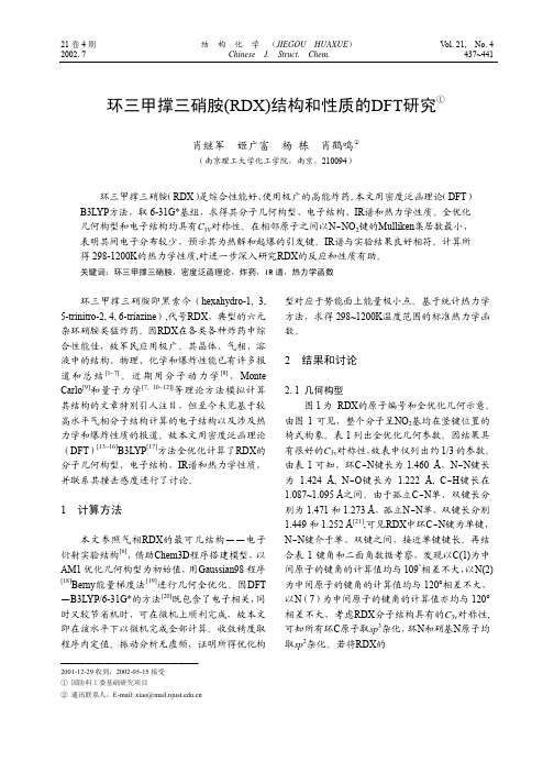
环三甲撑三硝胺(RDX)结构和性质的DFT研究①
438
结 构 化 学(JIEGOU HUAXUE) Chinese J. Struct. Chem.
2002 Vol. 21
全优化分子几何构型与气相RDX分子结构[6]作比 较,则发现二者极为接近,两者键长差值最大为 0.001Å,两者键角差值最大为 8.1°。考虑到所用 基组的近似性,以及在电子衍射实验数据分析中
B3LYP 115.6 112.7 117.4 127.O 110.0
角(°) EXP[6] 123.7 109.4 116.3 125.5 105.1
二
面
D(C1–N2–C3–N4) D(C3–C1–N2–N7)
D(N2–N7–O8–O9)
D(C1–N2–N7–O8) D(C1–N2–N7–O9)
表 1. RDX 的 B3LYP/6-31G*全优化几何参数 Table 1. The Full Optimized Geometric Parameters for RDX at B3LYP/6-31G* Level
键
R(C1–N2) R(N2–C3) R(CN) R(N2–N7) R(NN) R(N7–O8) R(N7–O9) R(NO) R(C1–H16) R(C1–H17) R(CH)
由图 1 可见,整个分子呈NO2基均在竖键位置的 椅式构象。表 1 列出全优化几何参数。因结果具 有很好的C3v对称性,故表中仅列出约 1/3 的参数。 由表 1 可知,环CN键长为 1.460 Å,NN键长 为 1.424 Å, NO键长为 1.222 Å, CH键长在 1.087~1.095 Å之间。由于孤立CN单、双键长分 别为 1.471 和 1.273 Å,孤立NN单、双键长分别 1.449 和 1.252 Å[21],可见RDX中环CN键为单键, NN键介于单、双键之间,接近单键键长。再结 合表 1 键角和二面角数据考察,发现以C(1)为中 间原子的键角的计算值均与 109°相差不大,以N(2) 为中间原子的键角的计算值均与 120°相差不大, 以N(7)为中间原子的键角的计算值亦均与 120° 相差不大,考虑RDX分子结构具有的C3v对称性, 可知所有环C原子取sp3杂化,环N和硝基N原子均 取sp2杂化。若将RDX的
- 1、下载文档前请自行甄别文档内容的完整性,平台不提供额外的编辑、内容补充、找答案等附加服务。
- 2、"仅部分预览"的文档,不可在线预览部分如存在完整性等问题,可反馈申请退款(可完整预览的文档不适用该条件!)。
- 3、如文档侵犯您的权益,请联系客服反馈,我们会尽快为您处理(人工客服工作时间:9:00-18:30)。
元器件交易网
Dielectric Ceramic Filters and Duplexers
Applications
Satellite Receivers-Down Converters Global Positioning Systems Wireless LAN Equipment Cellular and Cordless Phones
4.0
4.0
RCFC1 Package
Part Number RCFC2-813BP4 RCFC2-813BP4 RCFC2-813BP4
Center Frequency Bandwidth Insertion Loss (Max) Ripple (Max) V.S.W.R (Max) Attenuation (Min) 3.5 dB 0.5 dB 2 30 dB @ Fo±40 MHz 813.0 MHz F0±5 MHz 836.5 MHz F0±12.5 MHz 20 dB @ Fo±32.5 MHz 3.0 dB 0.8 dB 2 881.5 MHz
Bandwidth Insertion Loss (Max) Ripple (Max) V.S.W.R (Max) F0±16.5 MHz F0±12.5 MHz F0±13.0 MHz F0±17.5 MHz 3.0 dB 2.6 dB 3.0 dB 3.0 dB 1.3 dB 1.0 dB 1.0 dB 1.3 dB 2 2 2 2
2.3
2.7
3.0
Attenuation (Min) 7 dB @ Fo±28.5 MHz 12 dB @ Fo±32.5 MHz 12 dB @ Fo±32.5 MHz 6 dB @ Fo±28.5 MHz
Applications for RCFB2
GSM E-TACS ISM915 E-GSM
5.0 14.5 3.1
4.5 MAX
1.7
4.6
1.7
CONDUCTIVE METAL (GROUND) CONDUCTIVE METAL (IN-OUT)
RCFA Package
Raltron Electronics Corporation 10651 NW 19th St. Miami, Florida 33172 U.S.A. Tel: 305-593-6033 Fax: 305-594-3973 e-mail: sales@ Internet:
T
元器件交易网
Dielectric Ceramic Filters
Specifications
5 Pole Bandpass Filter
Part Number RCFD1-1310BP5 RCFD1-1950BP5 RCFD1-2140BP5 RCFD1-2800BP5 RCFD1-836BP5 RCFD1-881BP5 RCFD1-808BP5 RCFD1-852BP5 RCFD1-1690BP5 RCFD1-1972BP5 Center Frequency 1310.0 MHz 1950.0 MHz 2140.0 MHz 2800.0 MHz 836.5 MHz 881.5 MHz 808.0 MHz 852.0 MHz 1690.0 MHz 1972.0 MHz Bandwidth Insertion Loss (Max) Ripple (Max) V.S.W.R (Max) F0±17.5 MHz 4.1 dB 1.6 dB 2 F0±30.0 MHz F0±1000 MHz F0±12.5 MHz F0±5.0 MHz F0±25.0 MHz F0±2.5 MHz 3.0 dB 3.0 dB 3.0 dB 4.5 dB 4.0 dB 5.0 dB 1.0 dB 1.6 dB 1.0 dB 1.0 dB 1.0 dB 0.5 dB 1.5 2 2 2 2 2 Attenuation (Min) 12 dB @ Fo±28 MHz 40 dB @ 2070 MHz 40 dB @ 2260 MHz 60 dB @ Fo±1000 MHz 28 dB @ Fo±32.5 MHz 50 dB @ Fo±45 MHz 50 dB @ Fo±140 MHz 25 dB @ Fo±32.5 MHz
10.0 ALL DIMENSIONS ARE MM TOLERANCE IS ±0.3 MM 4.3 MAX 1.0 1.5 2.0 4.0 CONDUCTIVE METAL (GROUND) CONDUCTIVE METAL (IN-OUT)
RCFB2 Package
Raltron Electronics Corporation 10651 NW 19th St. Miami, Florida 33172 U.S.A. Tel: 305-593-6033 Fax: 305-594-3973 e-mail: sales@ Internet:
Outline Drawings
2.0
Applications for RCFB1
1.9
1.6 1.7 0.9 1.9 1.0 1.7 1.2
LMR E-Amps CT-2
MARKING AREA
10.0
7.0 ALL DIMENSIONS ARE MM TOLERANCE IS ±0.3 mm
4.5 MAX
1.5
0.9
1.5 1.2
MARKING AREA
4.4
元器件交易网
Dielectric Ceramic Filters
Specifications
4 Pole Bandpass Filter
Part Number RCFC1-1930BP4 RCFC1-2120BP4 RCFC1-2315BP4 RCFC1-2385BP4 Center Frequency Bandwidth Insertion Loss (Max) Ripple (Max) V.S.W.R (Max) 1930.0 MHz F0±10.0 MHz 4.5 dB 0.8 dB 2 2120.0 MHz 2315.0 MHz F0±15.0 MHz 4.5 dB 1.0 dB 1.8 2385.0 MHz Attenuation (Min) 40 dB @ Fo±70 MHz 40 dB @ Fo±90 MHz
1.9
2.4 1.1
4.3
9.6
元器件交易网
Dielectric Ceramic Filters
Specifications
3 Pole Bandpass Filter
Part Number Center Frequency 815.0 MHz RCFB1-815BP3 860.0 MHz RCFB1-860BP3 836.5 MHz RCFB1-836BP3 881.5 Mhz RCFB1-881BP3 841.0 MHz RCFB1-841BP3 866.0 MHz RCFB1-866BP3 948.0 MHz RCFB1-948BP3 Bandwidth Insertion Loss (Max) Ripple (Max) V.S.W.R (Max) F0±10.0 MHz F0±12.5 MHz F0±2.0 MHz F0±4.0 MHz 2.8 dB 3.0 dB 3.0 dB 3.0 dB 0.8 dB 1.0 dB 0.3 dB 0.5 dB 2 2 2 2 Attenuation (Min) 36 dB @ Fo±80 MHz 12 dB @ Fo±32.5 MHz 44 dB @ Fo±75 MHz 32 dB @ Fo±50 MHz
IN-OUT
RCFC2 Package RCFC2 Package
Raltron Electronics Corporation 10651 NW 19th St. Miami, Florida 33172 U.S.A. Tel: 305-593-6033 Fax: 305-594-3973 e-mail: sales@ Internet:
Outline Drawings Applications for RCFC1
4.5 4.5 4.6
IMT-2000 WLL
7.4 13.0
2.8
2.8
MARKING AREA
13.6 ALL DIMENSIONS ARE MM TOLERANCE IS ±0.3 MM
4.5 MAX
2.8
1.0 1.1 EXPOSED METAL (IN-OUT) EXPOSED METAL (GROUND) SOLDER MASK
1.0 1.5 1.5 1.1 1.0
O N M
P
Q
R
Applications for RCFC2
TRS AMPS
S
V
16.99
MARKING AREA L I 0.0 25.65 ALL DIMENSIONS ARE MM TOLERANCE IS ±0.3 MM 7.5 MAX IN-OUT
U 0.0
RCFand RDX Series
Features
Wide Frequency Range of 600 to 2500 MHz High Q Resonator Excellent Temperature Stability and Attenuation Low Insertion Loss Custom Designs for Application Specific Products