SDM15010中文资料
SD51;中文规格书,Datasheet资料

Major Ratings and Characteristics SCHOTTKY RECTIFIER60 AmpSD51Bulletin PD-2.327 rev. C 11/02TO-203AB (DO-5)SD512Bulletin PD-2.327 rev. C 11/02T J Max. Junction Temperature Range -65 to 150°C T stgMax. Storage Temperature Range-65 to 150°C R thJC Max. Thermal Resistance Junction1.0°C/W DC o peration * See Fig. 4to Case R thCS Typical Thermal Resistance, Case to0.25°C/WMounting surface , smooth and greasedHeatsink wt Approximate Weight 15 (0.53)g (oz.)TMounting T orque Min.23 (20)Non-lubricated t hreads Max.46 (40)Case S tyleDO-203AB(DO-5)JEDECKg-cm (Ibf-in)Thermal-Mechanical SpecificationsParametersSD51UnitsConditionsV FMMax. Forward Voltage Drop (2)0.58V @ 35A * See Fig. 10.66V @ 60A 0.86V @ 120A 0.75V @ 120A I RM Max. Reverse Leakage Current (2)50mA T J = 25 °C * See Fig. 2200mA T J = 125 °CC T Max. Junction Capacitance 2900pF V R = 5V DC , (test signal range 100Khz to 1Mhz) 25 °C L STypical Series Inductance7.5nH Measured from top of terminal to mounting planedv/dt Max. Voltage Rate of Change10000V/ µs(Rated V R )V R = rated V RElectrical SpecificationsParametersSD51UnitsConditions(2) Pulse Width < 300µs, Duty Cycle < 2%T J = 150 °C T J = 25 °C I F(AV)Max. Average Forward Current60A 50% duty cycle @ T C = 90°C, rectangular wave form * See Fig. 5I FSMMax. Peak One Cycle Non-Repetitive 800A60Hz half cycle sine wave Surge Current * See Fig. 7or 5ms rectangular pulseParametersSD51 UnitsConditionsAbsolute Maximum RatingsFollowing any rated load condition and with rated V RRM appliedPart numberSD51V RMax. DC Reverse Voltage (V)V RWM Max. Working Peak Reverse Voltage (V)45(1)Voltage Ratings* For Additional Informations and Graphs, Please See the 50HQ Series(1) For SD51 V RWM and V RRM = 45V @ T J = 25°C , =35V @ T J = 150°CSD513Bulletin PD-2.327 rev. C 11/02SD514Bulletin PD-2.327 rev. C 11/024812160102030405060708090A l l o w a b l e C a s e T e m p e r a t u r e - (°C )A v e r a g e F o r w a r d C u r r e n t - I (A )F (A V)5101520253004080120160200A v e r a g e P o w e r L o s s - (W a t t s )F (A V )A v e r a g e F o r w a r d C u r r e n t - I (A )Fig. 5 - Maximum Allovable Case TemperatureVs. Average Forward CurrentFig. 6 - Forward Power Loss Characteristics10100100010100100010000pF S MN o n -R e p e t i t i v e S u r g e C u r r e n t - I (A )S q u a r e W a v e P u l s e D u r a t i o n - t (m i c r o s e c )Fig. 7 - Max. Non-Repetitive Surge CurrentIR WORLD HEADQUARTERS: 233 Kansas St., El Segundo, California 90245, USA Tel: (310) 252-7105TAC Fax: (310) 252-7309Visit us at for sales contact information. 11/02Data and specifications subject to change without notice.This product has been designed for Industrial Level.Qualification Standards can be found on IR's Web site.分销商库存信息: VISHAYSD51。
SDM1001 地埋式垃圾桶
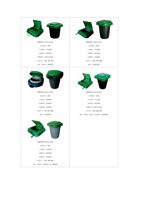
SDM1001 地埋式垃圾桶
有效容积:120L
上盖材料:冷轧钢板
内胆材料:镀锌钢板
外桶材料:防腐复合树脂
外形尺寸:750×750×750
备注:带防扒、减震装置
SDM1002 地埋式垃圾桶
有效容积:120L
上盖材料:冷轧钢板
内胆材料:镀锌钢板
外桶材料:高强塑胶
外形尺寸:640×640×850
备注:带减震装置
SDM1003 地埋式垃圾桶
有效容积:120L
上盖材料:高强塑胶
内胆材料:高强塑胶
外桶材料:高强塑胶
外形尺寸:730×705×800
备注:防滑脚踏板
SDM1004 地埋式垃圾桶
有效容积:120L
上盖材料:冷轧钢板
内胆材料:镀锌钢板
外桶材料:防腐复合树脂
外形尺寸:665×665×900
备注:带防扒、减震、助力装置,防滑脚踏板
SDM1005 地埋式垃圾桶
有效容积:120L
上盖材料:冷轧钢板
内胆材料:镀锌钢板
外桶材料:高强塑胶
外形尺寸:705×705×900
备注:带防扒、减震装置,防滑脚踏板。
SDM10M45SD-7-F;SDM10M45SD-7;中文规格书,Datasheet资料
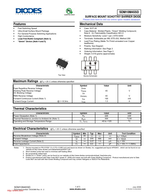
SURFACE MOUNT SCHOTTKY BARRIER DIODEFeatures• Fast Switching Speed• Ultra-Small Surface Mount Package• For General Purpose Switching Applications• High Conductance• Lead Free/RoHS Compliant (Note 3)• "Green" Device (Note 4 and 5)Mechanical Data• Case: SOT-26• Case Material: Molded Plastic, "Green" Molding Compound,Note 6. UL Flammability Classification 94V-0• Moisture Sensitivity: Level 1 per J-STD-020D• Terminals: Solderable per MIL-STD-202, Method 208• Lead Free Plating (Matte Tin Finish annealed over Copperleadframe).• Polarity: See Diagram• Marking Information: See Page 3• Ordering Information: See Page 3• Weight: 0.016 grams (approximate)Top View Device SchematicMaximum Ratings@T A = 25°C unless otherwise specifiedCharacteristic Symbol Value Unit Peak Repetitive Reverse VoltageWorking Peak Reverse VoltageDC Blocking VoltageV RRMV RWMV R45 VRMS Reverse Voltage V R(RMS)40 VForward Continuous Current (Note 1) I FM100 mAForward Surge Current @ t < 8.3ms I FSM 1.0 AThermal CharacteristicsCharacteristic Symbol Value Unit Power Dissipation (Note 1) P D225 mWThermal Resistance Junction to Ambient Air (Note 1) RθJA444 °C/WOperating and Storage Temperature Range T J , T STG-40 to +125 °CElectrical Characteristics@T A = 25°C unless otherwise specifiedCharacteristic Symbol Min Typ Max Unit Test Condition Reverse Breakdown Voltage (Note 2) V(BR)R45 ⎯⎯⎯I R = 100μAForward Voltage V F⎯370 450 mV I F = 10mAReverse Leakage Current (Note 2) I R⎯0.07 1.0 μA V R = 10VTotal Capacitance C T⎯ 6.0 ⎯pF V R = 10V, f = 1.0MHz Notes: 1. Device mounted on FR-5 PCB 1.0 x 0.75 x 0.062 inch pad layout as shown on Diodes, Inc. suggested pad layout AP02001, which can be found on our website at /datasheets/ap02001.pdf.2. Short duration pulse test used to minimize self-heating effect.3. No purposefully added lead.4. Diodes Inc.'s "Green" policy can be found on our website at /products/lead_free/index.php.5. Product manufactured with Date Code 0627 (week 27, 2006) and newer are built with Green Molding Compound. Product manufactured prior to DateCode 0627 are built with Non-Green Molding Compound and may contain Halogens or Sb2O3 Fire Retardants.SDM10M45SDDocument number: DS30386 Rev. 6 - 21 of 3July 2008© Diodes Incorporated /Please click here to visit our online spice models database.10203040V , INSTANTANEOUS REVERSE VOLTAGE (V)Fig. 2 Typical Reverse Characteristics R 100101.00.10.011,0001.010100I , I N S T A N T A N E O U S F O R W A R D C U R R E N T (m A )F V , INSTANTANEOUS FORWARD VOLTAGE (V)Fig. 1 Typical Forward Characteristics F1.010C , T O T A L C A P A C I T A N C E (p F )TV , DC REVERSE VOLTAGE (V)Fig. 3 Total Capacitance vs. Reverse Voltage, Per Element R2040255075100125150I A V E R A G E R E C T I F I E D C U R R E N T (m A )O ,T , AMBIENT TEMPERATURE (C)Fig. 4 Forward Current Derating Curve (Per Element)A °6080100 050100150200250P , P O W E R D I S S I P A T I O N (m W )D T , AMBIENT TEMPERATURE (C)Fig. 5 Power Derating CurveA °SDM10M45SDDocument number: DS30386 Rev. 6 - 22 of 3July 2008© Diodes Incorporated/Ordering Information (Notes 5 & 6)Part Number Case Packaging SDM10M45SD-7-FSOT-26 3000/Tape & ReelNotes: 6. For packaging details, go to our website at /datasheets/ap02007.pdf.Marking InformationKLG YM K L G Y MKLG = Product Type Marking CodeYM = Date Code Marking Y = Year ex: P = 2003M = Month ex: 9 = SeptemberDate Code KeyYear 2003 2004 2005 2006 2007 2008 2009 2010 2011 2012 2013 2014 2015 Code P R S T U V W X Y Z A B CMonth Jan Feb MarAprMay Jun Jul Aug Sep Oct Nov DecCode 1 2 3 4 5 6 7 8 9 O N DPackage Outline Dimensions SDM10M45SDDocument number: DS30386 Rev. 6 - 23 of 3July 2008© Diodes IncorporatedSuggested Pad LayoutIMPORTANT NOTICEDiodes Incorporated and its subsidiaries reserve the right to make modifications, enhancements, improvements, corrections or other changes without further notice to any product herein. Diodes Incorporated does not assume any liability arising out of the application or use of any product described herein; neither does it convey any license under its patent rights, nor the rights of others. The user of products in such applications shall assume all risks of such use and will agree to hold Diodes Incorporated and all the companies whose products are represented on our website, harmless against all damages.LIFE SUPPORTDiodes Incorporated products are not authorized for use as critical components in life support devices or systems without the expressed written approval of the President of Diodes Incorporated.SOT-26Dim Min Max Typ A 0.35 0.500.38 B 1.50 1.70 1.60 C 2.70 3.00 2.80 D ⎯ ⎯ 0.95 H 2.90 3.10 3.00 J 0.0130.100.05 K 1.00 1.30 1.10 L 0.35 0.550.40 M 0.10 0.200.15α 0° 8° ⎯All Dimensions in mmXZYCEEGDimensions Value (in mm)Z 3.20 G 1.60 X 0.55 Y 0.80C2.40E0.95/分销商库存信息:DIODESSDM10M45SD-7-F SDM10M45SD-7。
vW01105-1-2010版本
Resistance Spot WeldingDesign, CalculationUncoated and Coated Steel SheetsPrevious issuesVW 01105-1: 1977-05, 1993-12, 2003-05, 2003-06, 2003-11, 2007-03ChangesThe following changes have been made as compared to VW 01105-1: 2007-03:–Technical responsibility changed–Appendix A "Limits for quality levels" added–Referenced standards updatedContents PageScope (2)Terms and definitions (3)Spot welding (3)Heat-affected zone HAZ .............................................................................................3Unaffected base material (3)Design (3)Spot-welded joint (3)Weld joint (3)Sheet thickness (3)Requirements (3)Materials (welding suitability) (5)Design (weld reliability) (6)Position of the weld spots ..........................................................................................6122.12.22.32.42.4.12.4.22.4.333.13.23.2.1Group Standard VW 01105-1Issue 2010-02Class. No.:04815Descriptors:welding, spot welding, resistance spot welding, weld spot, sheet metal, steel, sheet steelCheck standard for current issue prior to usage.This electronically generated standard is authentic and valid without signature.The English translation is believed to be accurate. In case of discrepancies the German version shall govern.Numerical notation acc. to ISO practice.Page 1 of 32Technical responsibility Standards DepartmentGQL-LM1Dr. Knud Nörenberg Tel.: +49-5361-9-73623GQL-LM Dr. Stephan Eisenberg EKDV/4 Uwe Fischer EKDVTel.: +49-5361-9-27995Manfred Terlinden Confidential. All rights reserved. No part of this document may be transmitted or reproduced without prior permission of a Standards Department of the Volkswagen Group.Parties to a contract can only obtain this standard via the B2B supplier platform .© Volkswagen Aktiengesellschaft VWNORM-2008-12l QU E L L E : N O L I SWeld sequence ..........................................................................................................7Arrangement of spots (spot position) .........................................................................7Spot spacing ..............................................................................................................7Design examples and dimensions .............................................................................8Tolerances ...............................................................................................................13Manufacturing (welding capability) ...........................................................................14Basics .......................................................................................................................16Minimum shear force (F S ) .........................................................................................16Cross-tension force F K .............................................................................................17Peeling force F peel .....................................................................................................17Torsion .....................................................................................................................18Static and dynamic loads .........................................................................................18Process assurance ...................................................................................................19Weld spot geometry .................................................................................................19Number of weld spots ..............................................................................................23Surface quality class for spot-welded sheets ...........................................................23Drawing entries ........................................................................................................24Referenced documents ............................................................................................25Limit values for quality levels ...................................................................................263.2.23.2.33.2.43.2.53.2.63.344.14.24.34.44.54.64.6.14.6.24.6.356Appendix AScopeThe following basic regulations are based on experience with low to high degrees of mechanization,on test results, as well as on standards and technical regulations, e.g. DVS 2902-1, DVS 2902-2,DVS 2902-3.This standard is used for the design, calculation and workmanship of resistance-spot-welded sheet steel constructions subject to both static and dynamic loads. The joints used in these constructions are hereinafter referred to as "spot-welded joints".This standard covers resistance spot welding (reference number 21 acc. to DIN EN ISO 4063) on single-shear spot-welded joints with a sheet thickness ratio ≤ 3 : 1 for a thickness of 0,5 mm to 4,0 mm,as well as quality characteristics of single-spot and multiple-spot-welded joints. Larger sheet metal thicknesses and ratios are possible in agreement with the engineering departments. The nugget diameter is always determined by the thinnest sheet thickness.Sheets according to DIN EN 10139, however, are to be used only if their thickness does not exceed 3,0 mm.The introduction of zinc-coated sheets, e.g., according to DIN EN 10142 or DIN EN 10292, and the use of high-strength and higher-strength steels require higher electrode forces. This, in turn, may result in the necessity for larger electrode tip and electrode shank diameters (16 mm and 20 mm).When these electrodes are used, the weld nugget moves further away from the root face in the case of angled spot-welded flanges. However, as the distance between the weld nugget and the root face increases, component rigidity and strength decrease.Further requirements for (resistance) spot-welded joints are included in:–VW 01105-2 Resistance Spot Welding; Aluminum Materials,–VW 01105-4 Multiple-Sheet Joints; Dual- and Multiple-Shear JointsThe procedures described in the Test Specifications PV 6702 and PV 6717 are decisive for the quality audit of spot-welded joints.1 Page 2VW 01105-1: 2010-02Terms and definitions Spot weldingIn resistance spot welding, the weld zone between the parts to be joined is heated to the melting point using resistance heating with electrode force acting simultaneously. Size, shape and position of the melted base material depend on the temporal and spatial interaction of the heat quantities generated and dissipated in the weld zone and its surroundings. Under the influence of the electrode force, the workpieces are joined when the melt solidifies. The welded joint in the shape of a "weld nugget" that develops during this process is referred to as a …weld spot“ (Figure 26) that joins the parts (Section 2.4.2). The nugget diameter d L is the diameter of the melted material in the joining plane that is measured on the microsection.Heat-affected zone HAZArea of the base material that remains solid but experiences changes in microstructure due to the thermal energy applied during spot welding.Unaffected base materialArea of the base material that has experienced no recognizable changes in microstructure due to the energy applied during spot welding.Base materials that do not differ significantly in their chemical composition and suitability for spot welding are considered materials of the same type. Base materials that differ significantly in their chemical composition and suitability for spot welding are considered as different types of materials.Design Spot-welded jointThe spot-welded joint is a connection of two or more parts joined directly at the weld joint by one or more "weld spots" or "spot seams". The parts involved are designated on drawings as an ASSY (assembly) or WA (welded assembly).Weld jointThe weld joint is the configuration in which the parts are joined to each other by spot welding. The respective joint type is determined by the design relationships of the parts to each other.Sheet thicknesst 1 and t 2 are sheet thickness values of the single-shear spot-welded joint. For the purpose of uniform definition, especially for calculation, the thinnest sheet or the thinnest outer sheet of the joint must always be designated as t 1 if there are different sheet thicknesses. The thickest sheet of the joint is designated as t 2.RequirementsEach spot-welded construction must be "suitable for welding" in order to achieve the greatest possible design strength during manufacturing in the sense of the design goal with adequate safety and op‐timum cost-quality ratio. This means that the dimensions in the spot welding equipment, the electrode 22.1 2.2 2.3 2.42.4.1 2.4.2 2.4.3 3 Page 3VW 01105-1: 2010-02space requirement, as well as the accessibility of the workpiece must already be taken into consid‐eration during advance engineering. The weldability depends on three influencing variables:–welding suitability (material),–weld reliability (design),–welding capability (manufacturing).All three criteria have the same priority for weldability, see Figure 1. For a definition, please also refer to DIN Technical Report ISO/TR 581 "Weldability - Metallic Materials, General Principles".Figure 1 – Schematic representation of the weldability of spot-welded jointsPage 4VW 01105-1: 2010-02Materials (welding suitability)The welding suitability is a material property. Materials are suitable for welding if the material´s chemical composition allows a welded joint that meets the requirements set forth in the respective standards to be produced.For a first estimation of the welding parameters of a joining task, it is recommended to prepare a weldability lobe (time/current diagram, Figure 2) stating the limit lines for the minimum and maximumnugget or spot diameters for a constant electrode force and shape, see also DIN EN ISO 14327.Figure 2 – Weldability lobeFor estimation of the welding parameters, it is recommended to select the welding time and current values such that the following current differences result between the limit lines of d L min or d P min and d L max or d P max :–Δ ≥ 1,2 kA for resistance spot welding equipment with tip cutting device,–Δ ≥ 1,5 kA for resistance spot welding equipment without tip cutting device.The chemical composition basically influences the microstructure, hardening, nugget formation and strength of the spot-welded joint.The less the material-related factors have to be considered in manufacturing and design, the greater the welding suitability of a material within a material group (see DVS 2902-2).Testing of nugget position, nugget shape, and welding range is required for spot-welded joints of mixed materials (especially connections between unalloyed/low-alloyed steels and austenitic steels).All steels with a C content of up to 0,25% (max. 0,3%) are suitable for spot welding. In many cases,the equivalent carbon content (CE) is used for determining the welding suitability (hardening) of un‐alloyed and low-alloyed steels. According to DVS 2902-2, the following equation applies to a first estimation of the hardening of the weld metal:CE = C + Mn/6(1)3.1 Page 5VW 01105-1: 2010-02Figure 3 – Maximum hardness of the weld nugget as a function of the equivalent carbon content Figure 3 is an example illustrating the interdependence between the maximum hardness of the weld nugget and the equivalent carbon content.Special measures (e.g. reheating, multi-pulse welding, etc.) may be necessary for alloyed steels due to the alloying elements that influence hardness. Therefore, their use has to be agreed upon with the responsible engineering departments and tested separately.A hardness increase factor of ≤ 3,5 is recommended as the limit value for the hardness in both the weld nugget and the HAZ.Example:(2)The maximum hardness in the weld nugget and the HAZ must not exceed the value of 550 HV 0,2.See also DVS 2905.Design (weld reliability)Weld reliability is of particular importance for design. The design-related weld reliability is mainly influenced by the material and to a slight extent by manufacturing. Weld reliability is provided if, with the material used, a component remains functional under the intended operating conditions due to its design.Position of the weld spotsThe position of the weld spots must be specified by Design Engineering in consultation with Produc‐tion and Planning departments. If possible, the electrodes should contact the part perpendicular to the part surface. Otherwise, i.e. if they contact the part surface at a different angle, the nugget diam‐eter may be significantly smaller and elliptical.3.2 3.2.1 Page 6VW 01105-1: 2010-02The key criteria for the distance between the weld spot and the perpendicular flange are the minimum distance A = 2,0 mm from the current-carrying parts, the largest radius R i , as well as the electrode shank diameter d S or electrode tip diameter d K .Please refer to the drawing or DIN ISO 2768-1 for positional tolerances of the weld spots (spot spacing tolerance).Further information on the design of spot-welded joints can be obtained from DVS 2902-3.Weld sequenceContinuous rows of weld spots created using only one welding device must have spacings no smaller than 25 mm. For narrower spot spacings, the welding to gap method must be used (to prevent sub‐sequent spots from being too small or loose, see Figure 4).Arrangement of spots (spot position)The arrangement of spots must be selected such that the force F to be transferred is distributed as uniformly as possible over all spots. If the load distribution is not uniform, there will be a negative effect on both the vibration resistance and the crash behavior.With multiple-row spot seams, the spot arrangement is to be agreed upon with the Design Engineer‐ing, Calculation, Strength, Planning and Production departments.Spots that cannot be welded properly due to difficult accessibility are to be avoided (see Figure 7)."Quarter, third, half and three-quarter spots" reduce load bearing capacity. In checked exceptional cases, a defined portion of half and three-quarter spots can be permitted by the Testing department (Vehicle Strength and Vehicle Safety) in certain areas. This must be noted separately in the assembly drawing (Figure 29).Spot spacing The spot spacing e is the distance between the centers of two adjacent weld spots (Figure 4 and Figure 5). The spot spacing e Neb indicates the distance below which the shunt can no longer be ignored during the welding process.The shunt increases when–spot diameter,–sheet thickness,–electrode force, and –electrode contact surface increase, and when –the spot spacing decreases.Depending on the size of the shunt, the welding current must be increased more or less in order to create weld nuggets with the same diameter. The portion of the current that flows over spots of the seam that are already present does not contribute to heating the actual weld area. Therefore, the nugget diameter will be smaller starting from the 2nd spot of a seam if the spot spacing is too small and the setting data are constant. The influence of the shunt can be compensated for with the use of programmable and process-regulating controls. Generally, the following applies: e ≥ e Neb 4 x d L can be used as a reference value for the spot spacing e .Shunt can be ignored for a spot spacing e ≥ 10 (t 1 + t 2). In the case of multiple-row joints the following applies as a rule: e ≈ 5 x d L3.2.2 3.2.3 3.2.4 Page 7VW 01105-1: 2010-02Figure 4 – Left: double-row offset single-shear spot seam; right: double-row double-shear spot seam Figure 5 – Prevention of shunt in case of spot spacings that are too smallFigure 6 shows different forms of shunt.Figure 6 – Forms of shuntLegenda)Shunt at the sheet metal due to electrode contact b)Shunt via the centering pin (due to close distance)The Figure does not show shunt forms caused by c)clamps,dthe transformer grounding,e)the fixture.Design examples and dimensions Designs with poor accessibility are to be avoided, since specifically shaped electrodes and/or elec‐trode arms would be required (Figure 7 and Figure 12).3.2.5 Page 8VW 01105-1: 2010-02Figure 7 – Examples of unfavorable and favorable accessibility for the welding electrodes at the weldflangesOverlap Overlap b is the width of the contact surface of the weld flanges on the sections. The planes of thecontact surfaces must be parallel and touch each other (Figure 8).b is the shortest distance between the limit lines. The following applies: b ≥ 2v.Figure 8 – Left: single-row single-shear spot seam; right: double-row single-shear spot seamSeam spacing f For multiple-row spot seams, the seam spacing f is the shortest distance between the spot centers of adjacent seams (Figure 8 right). The following applies in general: f ≥ e.Seam length l The seam length l is the distance between the spot centers of the first and last spots of a spot seam (Figure 8).Edge distance v The edge distance v is the distance between the weld spot center and the closest limit line of the contact surface (Figure 9).3.2.5.1 3.2.5.2 3.2.5.3 3.2.5.4 Page 9VW 01105-1: 2010-02The following applies as a rule: v min = 1,25 x dL minFigure 9 – Edge distanceFlange width a The flange width a (Figure 10) is the value that is to be complied with in manufacturing, so that a)the position of the weld spot is not too close to the edge of the sheet metal,b)the welding equipment (electrode tip and shank) does not create any shunt to the bent sheet,c)the selected bending radius of the sheet is small enough to provide a longstraight portion of the flange width to ensure a sufficient contact surface forthe welding electrode.The flange width is to be agreed upon between Design Engineering, Planning and Production de‐partments.For calculation, see VW 01105-1 Supplement 1 "Resistance Spot Welding; Calculation of Flange Width ".In exceptional cases, it is possible to deviate from the flange width calculation. If this is the case, the flange width must be agreed upon between Design Engineering, Planning and Production depart‐ments.Figure 10 – Flange widthsFor multiple-row spot seams, the flange width a is to be increased according to the seam spacing f.The flange width is measured from the end of the flange to the angled sheet and is composed of the edge distance v and the clearance FM, as well as the tolerance T G .3.2.5.5 Page 10VW 01105-1: 2010-02Flange offset iThe flange offset i is the maximum projection of the primary flange with respect to the secondary flange, e.g. for the mounting of seals (Figure 10). The secondary flange must not protrude over the primary flange on the trim edge.Flange heights c and h, offset gThe dimensions c and h (Figure 10) take into consideration the dimensions of the spot weldingequipment, the electrode space requirements and the workpiece accessibility in manufacturing (see also Figure 13).The dimension g specifies the maximum permissible offset (Figure 11).The values must be agreed upon between Design Engineering, Planning and Production depart‐ments.Flange and overlap spacing kThe flange and overlap spacing k is the distance between overlap b and tangent line (Figure 11).Figure 11 – Offset g, spacing kThe following applies to k min : k ≥ 2,0 mm The following applies to g min : g ≥ sheet thickness3.2.5.6 3.2.5.73.2.5.8Flange geometryTable 1 – Weld flange geometry as a function of sheet thickness t min and welding condi‐tions (all dimensions in mm)Sheet thick‐nessSpot spacing Flange dimensions DiameterClearanceFlange width t mine Nebv min b min i g max k mind Kd SFMa0,5 to 0,6103,36,61,0–1,01,1213138,515,3> 0,6 to 0,8123,97,81,0–1,01,316181118,4> 0,8 to 1,0154,38,61,5–1,51,518,8> 1,0 to 1,2184,89,61,5–1,51,719,3> 1,2 to 1,5245,310,61,5–1,52,019,8> 1,5 to 1,6275,611,22,0–2,02,520,1> 1,6 to 2,0276,312,62,0–2,02,520201221,8> 2,0 to 2,5366,813,62,0–2,03,022,3> 2,5 to 3,0457,615,22,0–2,03,5241425,1> 3,0 to 3,5548,116,22,5–2,54,725,6> 3,5 to 4,0638,817,52,5–2,54,726,3Legend:v min = 1,25 d L min Edge distance (Figure 9) including tolerance b ≥ 2 v and b ≥ a - r Overlap (Figure 9)i Flange offset (Figure 10)g max Offset of the overlap (Figure 11)k min Flange and overlap spacing (Figure 11)d K Electrode tip diameter d SElectrode shank diameterFM = d S /2 + A Clearance for electrode shank diameter a ≥ v min + FM + T GFlange width, influence of electrode (f A=2; D shank )with T G = 3,5NOTE 1 Since the flange width values specified in Table 1 depend on several factors, and since at least T G must be agreed upon between Design Engineering, Planning and Production departments (see Section Section 3.2.6), the values still have to be corrected accordingly.Reference sheet thickness t vFor joints with different sheet thicknesses (t 1 ≠ t 2), the reference sheet thickness t v may be used instead of t min for determining the welding parameters.t v = 0,8 t 1 + 0,2 t 23.2.5.9 3.2.5.103.2.6TolerancesTolerance values must be agreed upon between Design Engineering, Planning and Production de‐partments.Trim tolerance T aThis value represents the trim tolerance during production of the individual part and must be included in the calculation.General body-in-white tolerance T RThis value considers the general tolerances in body construction, including the inaccuracies of in‐dustrial robots and must be included in the calculation.Design-related tolerance compensation T KThe value considers the flange displacements that are provided for secondary flanges and must be included in the calculation.Equipment tolerance T VThis value considers the repetition accuracy of the equipment and must be included in the calculation. Overall tolerance T GThe overall tolerance is made up of the tolerances T a, T R, T K and T V described above to the extent that these have to be considered.T G = T a + T R + T K + T VA total allowance of T G = 3,5 mm has been chosen for the calculation in Table 1.Manufacturing (welding capability)Care must also be taken in design to ensure that the component is capable of being welded (manu‐facturing-related weld reliability). It must be possible to produce the planned welds properly under the state-of-the-art manufacturing conditions.During the design of components, the following manufacturing aspects should be taken into consid‐eration:–If the designs require operating equipment with long arms spaced far apart, it must be determined early in the process whether the available welding equipment is suitable for this purpose.–If possible, the designs must allow short, straight and rigid arms, electrode brackets and elec‐trodes to be used (Figure 12).Figure 12 – Examples of electrode arm shapes to be avoided–Refer to VW 01105-4 for double-shear and multiple-shear joints.–The distance between the outer diameter of the electrode and/or the electrode bracket and theinner edge of the sheet must be at least (2 + 0,5) mm (Figure 13). Other specifications must be agreed upon between the responsible specialized departments.Figure 13 – Poor weld quality caused by electrodes that spring back and slide–During the welding process of high-strength and highest-strength sheets, the electrodes normally do not penetrate considerably into the base material. As a result, the risk of electrode sliding is increased. Especially if pneumatic electrode holder drives are used, it is important that the elec‐trodes are placed perpendicularly and that the electrode holder is as rigid as possible.–During welding of spot seams, the welding sequence must be selected such as to avoid the formation of cavities between the sheets (Figure 14).3.3Figure 14 – Welding sequence to avoid the formation of cavities–The electrode axis must be perpendicular to the sheet surface (90° ± 1°) (Figure 16, Figure 18).Figure 15 – Not per‐missible Figure 16 – Favor‐able Figure 17 – Permissi‐ble Figure 18 – Favor‐able–If asymmetrical electrode tips (Figure 17) are used, special measures are required in series production operation to ensure the proper alignment of the working surfaces (freedom from ro‐tation, orientation during tip change, special electrode tip milling cutters).BasicsDifferent types of loads occur depending on the design of a component (Section 2.4):–shear tension (Figure 19)–cross tension (Figure 20)–peeling tension (Figure 21)–torsion (Figure 22)If possible, spot-welded joints should only be loaded with shear tension since the highest forces per weld spot can be transferred with this type of load. Therefore, pure cross or peeling tensions and/or torsion are to be avoided.Minimum shear force (F S )For a single-shear joint, the shear force F s generates a bending moment M b = F s r s which increases with increasing load and also produces a portion of the cross tension force F K . r sis set as follows:Figure 19 – Shear tensionLegend A Prior to tensile testB After tensile test (exaggerated)C Outer notchF K Portion of the cross tension force of F max F SPortion of the shear force of F maxBecause of the realistic verification of requirements and the low variation of the test results, the cal‐culations of the spot-welded joints are based on the minimum shear force F s min that was determined from the shear test according to PV 6702:4 4.1F s min = F max - 2 s in kNLegend s Standard deviationF maxMean value of the maximum force determined in the shear test ac‐cording to DIN EN ISO 14273(3)Cross-tension force F KFigure 20 – Cross tensionWith this type of stress, the permissible load F K is only 60% of the shear force F min..The following applies according to DVS 2902-3 (to materials according to DIN EN 10130)F K ≤ 0,6 F min(4)Peeling force F peelFigure 21 – Peeling tensionWith this type of stress, the permissible load F peel perm is only 20% of the shear force F min as set forth in Table 2 and DVS 2902-3.F peel perm ≤ 0,2 F min(5)4.24.3TorsionFigure 22 – TorsionA durable joint is achieved with at least two weld spots, since, with twisting around one spot, the transferable torque M t is too low. Designs with only one load-bearing spot are not permissible.Static and dynamic loadsA basic distinction is made between calculations with static or dynamic loads. The formula relationship previously specified is used for calculation of static load.The following information applies to the proof of sufficient strength of dynamically loaded components:–Because of as yet inadequate knowledge about the influence of the design of the joint and the uncertainties in calculation, the load carrying capacity of the joints for vibration loads must always be verified through testing.–With a given material thickness, the service life of a joint depends on the load amplitude, the R value (stress ratio) and the type of load (Figure 23). The type of load may be shear or peeling.Cross tension and torsion usually do not occur. Generally no type of load occurs alone and in pure form.Figure 23 – Load amplitude–The single-row single-shear joint is to be preferred.–Dynamic cross tension, peeling tension and torsion are to be avoided due to the low permissible tension.4.4 4.5。
MPX5010-压力传感器

MPX5010Rev 11, 01/2007Freescale Semiconductor Technical Data© Freescale Semiconductor, Inc., 2007. All rights reserved.Integrated Silicon Pressure Sensor On-Chip Signal Conditioned, Temperature Compensated and CalibratedThe MPX5010/MPXV5010G series piezoresistive transducers are state-of-the-art monolithic silicon pressure sensors designed for a wide range of applications, but particularly those employing a microcontroller or microprocessor with A/D inputs. This transducer combines advancedmicromachining techniques, thin-film metallization, and bipolar processing to provide an accurate, high level analog output signal that is proportional to the applied pressure.Features• 5.0% Maximum Error over 0° to 85°C•Ideally Suited for Microprocessor or Microcontroller-Based Systems•Durable Epoxy Unibody and Thermoplastic (PPS) Surface Mount Package •Temperature Compensated over –40° to +125°C •Patented Silicon Shear Stress Strain Gauge•Available in Differential and Gauge Configurations•Available in Surface Mount (SMT) or Through-hole (DIP) Configurations Application Examples •Hospital Beds •HVAC•Respiratory Systems •Process ControlORDERING INFORMATIONDevice Type Options Case No.MPX Series Order No.Packing Options Device Marking SMALL OUTLINE PACKAGE (MPXV5010G SERIES)Basic Elements Gauge, Element Only, SMT 482MPXV5010G6U Rails MPXV5010G Gauge, Element Only, DIP 482B MPXV5010G7U Rails MPXV5010G Ported Elements Gauge, Axial Port, SMT 482A MPXV5010GC6U Rails MPXV5010G Gauge, Axial Port, DIP 482C MPXV5010GC7U Rails MPXV5010GGauge, Axial Port, SMT 482A MPXV5010GC6T1Tape & ReelMPXV5010GGauge, Side Port, SMT 1369MPXV5010GP Trays MPXV5010G Gauge, Dual Port, SMT 1351MPXV5010DP Trays MPXV5010GUNIBODY PACKAGE (MPX2202 SERIES)Basic ElementDifferential 867MPX5010D —MPXV5010D Ported Elements Differential, Gauge 867C MPX5010DP —MPXV5010DP Gauge 867B MPX5010GP —MPXV5010GPGauge, Axial 867E MPX5010GS —MPXV5010D Gauge, Axial PC Mount 867F MPX5010GSX —MPXV5010DMPX5010MPXV5010G SERIESUNIBODY PACKAGE PIN NUMBERS (1)1.Pins 4, 5, and 6 are internal device connections. Do not connect to external circuitry or ground. Pin 1 is noted by the notch in the lead.1V out 4N/C 2Gnd 5N/C 3V S6N/CSMALL OUTLINE PACKAGEPIN NUMBERS (1)1.Pins 1, 5, 6, 7, and 8 are internal deviceconnections. Do not connect to external circuitry or ground. Pin 1 is noted by the notch in the lead.1N/C 5N/C 2V S 6N/C 3Gnd 7N/C 4V out8N/CMPX5010SensorsFigure 1. Fully Integrated Pressure Sensor SchematicSensing ElementThin Film Temperature Compensationand Gain Stage #1Gain Stage #2and Ground Reference Shift CircuitryV SV outGNDPins 1 and 5 through 8 are NO CONNECTS for surface mount packagePins 4, 5, and 6 are NO CONNECTS for unibody packageTable 1. Maximum Ratings (1)1.Exposure beyond the specified limits may cause permanent damage or degradation to the device.RatingSymbol Value Unit Maximum Pressure (P1 > P2)P max 75kPa Storage Temperature T stg –40 to +125°C Operating TemperatureT A–40 to +125°CMPX5010SensorsTable 2. Operating Characteristics (V S = 5.0 Vdc, T A = 25°C unless otherwise noted, P1 > P2. Decoupling circuit shown in Figure 3 required to meet specification.)CharacteristicSymbol Min Typ Max Unit Pressure Range (1)1. 1.0 kPa (kiloPascal) equals 0.145 psi.P OP 0—10kPa Supply Voltage (2)2.Device is ratiometric within this specified excitation range.V S 4.75 5.0 5.25Vdc Supply CurrentI o — 5.010mAdc Minimum Pressure Offset (3)(0 to 85°C)@ V S = 5.0 Volts 3.Offset (V off ) is defined as the output voltage at the minimum rated pressure.V off0.20.425VdcFull Scale Output (4)(0 to 85°C)@ V S = 5.0 Volts 4.Full Scale Output (V FSO ) is defined as the output voltage at the maximum or full rated pressure.V FSO4.475 4.7 4.925VdcFull Scale Span (5)(0 to 85°C)@ V S = 5.0 Volts 5.Full Scale Span (V FSS ) is defined as the algebraic difference between the output voltage at full rated pressure and the output voltage at the minimum rated pressure.V FSS4.275 4.5 4.725VdcAccuracy (6)(0 to 85°C)6.Accuracy (error budget) consists of the following:•Linearity:Output deviation from a straight line relationship with pressure over the specified pressure range.•Temperature Hysteresis:Output deviation at any temperature within the operating temperature range, after the temperature is cycled toand from the minimum or maximum operating temperature points, with zero differential pressure applied.•Pressure Hysteresis:Output deviation at any pressure within the specified range, when this pressure is cycled to and from theminimum or maximum rated pressure, at 25°C.•TcSpan:Output deviation over the temperature range of 0° to 85°C, relative to 25°C.•TcOffset:Output deviation with minimum rated pressure applied, over the temperature range of 0° to 85°C, relative to25°C.•Variation from Nominal:T he variation from nominal values, for Offset or Full Scale Span, as a percent of V FSS , at 25°C.———±5.0%V FSS Sensitivity V/P —450—-mV/kPa Response Time (7)7.Response Time is defined as the time for the incremental change in the output to go from 10% to 90% of its final value when subjected to a specified step change in pressure.t R — 1.0—-ms Output Source Current at Full Scale Output I O+—0.1—-mAdc Warm-Up Time (8)8.Warm-up Time is defined as the time required for the product to meet the specified output voltage after the Pressure has been stabilized.——20—-ms Offset Stability (9)9.Offset Stability is the product's output deviation when subjected to 1000 hours of Pulsed Pressure, Temperature Cycling with Bias Test.——±0.5—-%V FSSTable 3. Mechanical CharacteristicsCharacteristicsTyp Unit Weight, Basic Element (Case 867) 4.0grams Weight, Basic Element (Case 482)1.5gramsMPX5010SensorsON-CHIP TEMPERATURE COMPENSATION, CALIBRATION AND SIGNAL CONDITIONINGThe performance over temperature is achieved by integrating the shear-stress strain gauge, temperature compensation, calibration and signal conditioning circuitry onto a single monolithic chip.Figure 2 illustrates the Differential or Gauge configuration in the basic chip carrier (Case 482). A fluorosilicone gel isolates the die surface and wire bonds from the environment, while allowing the pressure signal to be transmitted to the sensor diaphragm.The MPX5010 and MPXV5010G series pressure sensor operating characteristics, and internal reliability andqualification tests are based on use of dry air as the pressure media. Media, other than dry air, may have adverse effects onsensor performance and long-term reliability. Contact the factory for information regarding media compatibility in your application.Figure 3 shows the recommended decoupling circuit for interfacing the integrated sensor to the A/D input of amicroprocessor or microcontroller. Proper decoupling of the power supply is recommended.Figure 4 shows the sensor output signal relative to pressure input. Typical, minimum, and maximum output curves are shown for operation over a temperature range of 0° to 85°C using the decoupling circuit shown in Figure 3. The output will saturate outside of the specified pressure range.Figure 2. Cross-Sectional Diagram SOP(not to scale)Figure 3. Recommended Power Supply Decouplingand Output Filtering(For additional output filtering, please refer toApplication Note AN1646.)Figure 4. Output versus Pressure DifferentialFluoro Silicone Gel Die CoatWire Bond DieP1Stainless Steel CapThermoplasticCaseDie BondDifferential SensingElementP2+5 V1.0 µF0.01 µF470 pFGNDV sV outIPSOUTPUTLead FrameDifferential Pressure (kPa)O u t p u t (V )5.04.54.03.53.02.52.01.51.00.5001234567891110TYPICALMINMAXTransfer Function:V out = V S *(0.09*P+0.04) ± ERROR V S = 5.0 VdcTEMP = 0 to 85°CMPX5010SensorsNominal Transfer Value:V out = V S x (0.09 x P + 0.04)± (Pressure Error x Temp. Factor x 0.09 x V S )V S = 5.0 V ± 0.25 VdcTransfer Function (MPX5010, MPXV5010G)MPX5010, MPXV5010G SERIESTemp Multiplier–4030 to 851+1253Temperature in °C4.03.02.00.01.0–40–2020406014012010080Temperature Error FactorNOTE: The Temperature Multiplier is a linear response from 0° to –40°C and from 85° to 125°C.Temperature Error BandPressure Error (Max)Pressure Error Band0 to 10 (kPa)±0.5 (kPa)Pressure (kPa)0.50.40.2–0.3–0.4–0.501234567890.30.1–0.2–0.110Pressure Error (kPa)MPX5010SensorsPRESSURE (P1)/VACUUM (P2) SIDE IDENTIFICATION TABLEFreescale designates the two sides of the pressure sensor as the Pressure (P1) side and the Vacuum (P2) side. The Pressure (P1) side is the side containing fluorosilicone gel which protects the die from harsh media. The MPX pressuresensor is designed to operate with positive differential pressure applied, P1 > P2.The Pressure (P1) side may be identified by using the table below:MINIMUM RECOMMENDED FOOTPRINT FOR SURFACE MOUNTED APPLICATIONSSurface mount board layout is a critical portion of the total design. The footprint for the surface mount packages must be the correct size to ensure proper solder connection interface between the board and the package. With the correctfootprint, the packages will self align when subjected to a solder reflow process. It is always recommended to design boards with a solder mask layer to avoid bridging and shorting between solder pads.Figure 5. SOP Footprint (Case 482)Part NumberCase TypePressure (P1)Side IdentifierMPX5010D 867Stainless Steel Cap MPX5010DP 867C Side with Part Marking MPX5010GP 867B Side with Port Attached MPX5010GS 867E Side with Port Attached MPX5010GSX 867F Side with Port Attached MPXV5010G6U 482Stainless Steel Cap MPXV5010G7U 482B Stainless Steel Cap MPXV5010GC6U/T1482A Side with Port Attached MPXV5010GC7U 482C Side with Port Attached MPXV5010GP 1369Side with Port Attached MPXV5010DP1351Side with Part Marking0.66016.760.060 TYP 8X 1.520.100 TYP 8X 2.540.100 TYP 8X 2.540.3007.62inch mmSCALE 2:1CASE 482-01ISSUE OSMALL OUTLINE PACKAGECASE 482A-01ISSUE ASMALL OUTLINE PACKAGEMPX5010 SensorsCASE 482B-03ISSUE BSMALL OUTLINE PACKAGECASE 482C-03ISSUE BSMALL OUTLINE PACKAGEMPX5010SensorsCASE 867-08ISSUE NUNIBODY PACKAGEMPX5010 SensorsMPX5010SensorsMPX5010 SensorsCASE 867C-05ISSUE FUNIBODY PACKAGECASE 867E-03ISSUE DUNIBODY PACKAGEMPX5010SensorsCASE 867F-03ISSUE DUNIBODY PACKAGEMPX5010 SensorsMPX5010SensorsMPX5010 SensorsMPX5010SensorsMPX5010 SensorsMPX5010Rev. 11How to Reach Us:Home Page:Web Support:/support USA/Europe or Locations Not Listed:Freescale Semiconductor, Inc.Technical Information Center, EL5162100 East Elliot Road Tempe, Arizona 85284+1-800-521-6274 or +/supportEurope, Middle East, and Africa:Freescale Halbleiter Deutschland GmbH Technical Information Center Schatzbogen 781829 Muenchen, Germany +44 1296 380 456 (English)+46 8 52200080 (English)+49 89 92103 559 (German)+33 1 69 35 48 48 (French)/supportJapan:Freescale Semiconductor Japan Ltd.Headquarters ARCO Tower 15F1-8-1, Shimo-Meguro, Meguro-ku,Tokyo 153-0064Japan0120 191014 or +81 3 5437 9125support.japan@Asia/Pacific:Freescale Semiconductor Hong Kong Ltd.Technical Information Center 2 Dai King StreetTai Po Industrial Estate Tai Po, N.T., Hong Kong +800 2666 8080@For Literature Requests Only:Freescale Semiconductor Literature Distribution Center P .O. Box 5405Denver, Colorado 802171-800-441-2447 or 303-675-2140Fax: 303-675-2150LDCForFreescaleSemiconductor@Information in this document is provided solely to enable system and software implementers to use Freescale Semiconductor products. There are no express or implied copyright licenses granted hereunder to design or fabricate any integrated circuits or integrated circuits based on the information in this document.Freescale Semiconductor reserves the right to make changes without further notice to any products herein. Freescale Semiconductor makes no warranty, representation or guarantee regarding the suitability of its products for any particular purpose, nor does Freescale Semiconductor assume any liability arising out of the application or use of any product or circuit, and specifically disclaims any and all liability, including without limitation consequential or incidental damages. “Typical” parameters that may beprovided in Freescale Semiconductor data sheets and/or specifications can and do vary in different applications and actual performance may vary over time. All operating parameters, including “Typicals”, must be validated for each customer application by customer’s technical experts. Freescale Semiconductor does not convey any license under its patent rights nor the rights of others. Freescale Semiconductor products are not designed, intended, or authorized for use as components in systems intended for surgical implant into the body, or other applications intended to support or sustain life, or for any other application in which the failure of the Freescale Semiconductor product could create a situation where personal injury or death may occur. Should Buyer purchase or use Freescale Semiconductor products for any such unintended orunauthorized application, Buyer shall indemnify and hold Freescale Semiconductor and its officers, employees, subsidiaries, affiliates, and distributors harmless against all claims, costs, damages, and expenses, and reasonable attorney fees arising out of, directly or indirectly, any claim of personal injury or death associated with such unintended or unauthorized use, even if such claim alleges that Freescale Semiconductor was negligent regarding the design or manufacture of the part. Freescale™ and the Freescale logo are trademarks of Freescale Semiconductor, Inc.All other product or service names are the property of their respective owners.© Freescale Semiconductor, Inc. 2007. All rights reserved.。
(1-7)SDP-5100概述

指标参数 2kV、 3kV 2kV、 3kV 跌落到 50% >500ms
0% >100ms 6kV 接触 8kV 非接触 1.0kV、1MHz 2.5kV、1MHz
备注 GB6162 GB6162 GB6162 GB6162
触点容量
-2-
分、合闸出口继电器
述
组成装置的插件主要有:电源插件、交流采样插件、继电器插件、主板插件、液晶控制 及显示面板。各部件独立插接安装,散热好,抗干扰能力强,便于更换维护。
1) 硬件系统示意图
操作 按键、 分合 按键、 指示灯
大屏幕 LCD 显示器
外部开入量输入端子
人机接口板
操
作
面
主控板
板
控
制
板
电流电压变换器板 通讯板
电源及开入量板
2 主要特点及功能 2.1 保护功能齐备:各保护功能齐备,并可按照用户要求进行定制。 2.2 测量功能:高精度测量电流、电压、有功功率 、无功功率、功率因数、频率、零序电 流、计算电度;两路脉冲量输入实现外部电度表自动抄表。 2.3 高度集成:集保护、测量、控制、监测、通讯、录波、事件记录等多种功能于一体。 2.4 友好人机界面:大屏幕图形液晶显示,动态显示一次系统图、实时波形图、故障录波 图、各种电气参数及保护信息。中文菜单提示,操作快捷方便。 2.5 强大的通讯功能:提供 RS422/485 连网通讯接口。可实现遥测、遥信、遥控、保护定 值设定及查询、装置工作状态、SOE 事件记录、录波数据等传输功能。 2.6 多路状态监测功能;有多达 16 路开入量,除特殊定义外,其它开入量可由用户定义, 解决了用户需监测多个开入量问题,不需再配其他装置; 2.7 强大自检功能:具备软、硬件实时自检与报警功能。 2.8 在线编程功能(ISP):提供一个在线编程通讯接口,可自由下载各种保护软件模块、 一次系统图,无须拆卸装置。 2.9 SOE 事件记录: 在线记录事件量达 64 条,先进先出(FIFO)动态刷新,带有时间标记, 掉电不丢失。 2.10 故障录波功能:可将故障前、故障中、故障后的电流、电压、断路器状态和保护信息 完整真实记录下来,记录长度 100 个周波,为用户进行故障分析提供依据。
参考书MAG1103100-5100W-5000_6000cn[1]
![参考书MAG1103100-5100W-5000_6000cn[1]](https://img.taocdn.com/s3/m/8b86860cf12d2af90242e67e.png)
即插即用的模块界而。开放式的结构特性满足客户现有或 将来所需的通讯协议方式
4
SITRANS F M MAGFLO
1.产品介绍 1.2 工作方式
电 磁 流 量 计 依 据 法 拉 利 电 磁 感 应 原 理 设 计 。 流 量 计 由 传 感 器 MAG1100, MAG3100 或 MAG5100W 和信号转换器 MAG5000 或 MAG6000 组成。
输入电路模块
放大测量电极上的流体比例信号。输入阻抗极高:>1014Ω,允许介质电导率低至 1 ms/cm。 屏蔽电缆可消除山于电缆寄生电容所产生的测量误差。
数字信号处理器
转换模拟信号为数字信号并通过数字滤波抑制电极噪声。 信号转换器因长期工作漂移和温度漂移所产生的误差,由自动监视电路不间断补偿。模数转换 采用 23 bit 信号分辨率的超低噪声 ASIC,这使得不需采用量程切换。信号转换器的动态量程因而最
SITRANS F M MAGFLO
1.产品介绍
MAG 3100 高温型 PTFE
法兰(mm) 15 25 40 50 65 80 100 125 150 200 250 300 350 400 450 500 600
PN 6 N/A N/A N/A N/A LVD LVD LVD PED PED PED PED PED PED PED PED PED PED
PN100 SEP PED PED PED PED PED PED PED PED PED PED PED N/A N/A N/A N/A N/A N/A N/A N/A N/A N/A N/A N/A N/A N/A N/A N/A N/A
REF5010中文资料
UNLESS OTHERWISE NOTED this document contains PRODUCTION DATA information current as of publication date. Products conform to specifications per the terms of Texas Instruments standard warranty. Production processing does not necessarily include testing of all parameters.
Operating Temperature Range
Storage Temperature Range
Junction Temperature (TJ max)
ESD Rating
Human Body Model (HBM) Charged Device Model (CDM)
REF50xx +18 30
Excellent temperature drift (3ppm/°C) and high accuracy (0.05%) are achieved using proprietary design techniques. These features, combined with very-low noise make the REF50xx family ideal for use in high-precision data acquisition systems.
Each reference voltage is available in both standardand high-grade versions. They are offered in MSOP-8(3) and SO-8 packages, and are specified from –40°C to +125°C.
仪斯卡WQ MT860高精度关口电能表用户手册V1 3

WQ.MT860 高精度 关口电能表用户 培训手册 V1.3
文件编号: 版 日 本: 期:
EM-02-12 V1.3 2011-1-5
编 写: 校 对: 审 核: 批 准:
王元元 杨 帆
张玉玲 叶 军
工程部内部文件,请勿外传
WQ.MT860 高精度关口电能表用户培训手册 V1.2
上海惠安系统控制有限公司
文档历史记录
原稿编写人:王元元 发布时间:2006-12-30 修订记录: 版本 V1.1 V1.2 V1.3 修订时间 2008-8-4 2009-7-16 2011-1-5 修订人 陈申浩 何斌 曲岩 修订内容 增加抄表说明部分及其他细节完善 增加所有权编号注释 修改负荷曲线通道数、修改 3P3W 接线图 增加误差补偿、谐波、基波功能说明及应用
文件编号:EM-02-12
第 2 页 共 39 页
WQ.MT860 高精度关口电能表用户培训手册 V1.2
上海惠安 ................................................................................................................................................ 3 1.1 主要特点 ............................................................................................................................................3 1.2 60 年的表计制造历史 ..............................................
中仪电通 ZY5010 型 数字选频电平表 说明书

ZY5010型数字使用说明书目录1.概述 (1)2.电气和机械结构性能 (2)3.技术性能 (3)4.面板布置 (8)5.使用方法 (10)6.一般故障处理 (14)7.备附件 (15)8.售后服务 (15)ZY5010型数字选频电平表,适用于通信系统对基带特性的测试、电力载波和电力线保护设备的测试、高压输电线路、供电系统变电站对电力线载波通道进行衰减、串杂音等高频参数测试,以及电力通信结合设备高频阻波器、结合滤波器、高频电缆的开通维护测试,并满足实验室及教学的需求。
是一种新型的全键盘操作、全中文界面、LCD图形显示的高精度通信测试仪表。
本仪表和ZY5060型数字电平振荡器可配套组成载频传输测量仪。
仪表频率测量范围200Hz~1700kHz,包括从话路到300路群路的全部频段,分辨率1Hz,频率精度±3×10⁻⁶±1Hz。
频率调节全数字化,操作简便。
频率增量调节用户自由选择,最小步进1Hz。
选频测量具有25Hz和400Hz两种带宽,良好的选择性以及很低的固有失真,使电平表不仅仅作电平和串杂音测量,也可作波形分析。
本仪表为手提便携式结构,整体结构牢固,且体积小,重量轻,操作简便。
仪表长期使用稳定可靠,输入电平和频率精确度高。
内置可充电锂电池,交直流供电均可工作。
电池供电时连续工作时间约4小时,电池电量过低蜂鸣器自动告警提示用户对电池进行充电,非常适合野外现场使用。
符合原电子工业部标准SJ3210"A"档要求,环境条件符合GB6587.1中Ⅱ组规定。
1--2.电气和机械结构性能本仪表外形如图1所示。
图1ZY5010选频电平表外形图外形尺寸:270mm(宽)×120mm(高)×265mm(深)。
质量:2.4kg。
仪表面板布置简洁、美观,操作方便。
内部电路单元均为独立的印制板,印制板间采用扁平线缆连接,可靠性高,维修方便。
电源供给:本仪表交直流两用,直流电力消耗小于4W。
(sms)5010塔吊说明书
塔吊技术指导文件前言、第一步感谢您购买本公司的塔式起重机,为了帮助您了解塔机安装的性能,安全、快速地安装和正确地使用,以保证工程的顺利完成,请您仔细地阅读本技术指导文件,并按要求的方法制作。
、塔机第一次安装时,我公司派一名技术人员指导安装,您一定要聘请当地有安装资质的安装队伍安装,并拿我公司提供的资料向当地有关管理部门报检,我公司资料中有一回执单,请您认真填写并提出宝贵意见。
第一次和以后安装时,禁止夜间施工、本技术指导文件主要阐述最常用的安装形式,凡属下面情况之一者,应及时与我公司联系。
.塔机基础不能按本技术指导文件要求形式处理。
.塔机安装位置过于狭窄,以至于在拆塔机时,部件与建筑物发生干涉。
.塔机的起升高度超过技术指导文件要求。
、本公司致力于产品的不断完善,产品的某些局部结构或个别参数更改时,恕不另行通知。
如有疑问,请与本公司联系。
、建议使用单位应为塔机建立设备档案,档案应包括以下内容:.每次使用进度及安装地点。
.日常使用保养、维修、变更、检查和试验记录。
.设备故障记录。
.设备存在的问题和评价。
、客户自选配置(需加价):.驾驶室的冷、暖空调。
.风速仪。
.无线对讲机。
、三包条件:本公司不承担由以下原因造成的损坏、断裂和事故的任何法律责任: .塔机零、部件(包括备件、配件)不是由本公司提供的。
.塔机的更换式修理不是由具备修理塔机条件和级别证书的修造单位进行的。
.安装使用、拆卸和维修没有严格遵照使用技术指导文件。
及有关法律要求使用的。
.违反了法律制定的安全规则。
.因不可抗拒原因造成的(如:地震、台风、洪水、战争等)。
、塔机在使用期间,不得私自调节或拆除、限位安全装置,否则后果自负。
特别提示:在任一安全组织失灵的状态下,严禁使用!!!安全制作规程、司机应具备的条件:()司机应年满周岁,具初中以上文化程度。
()不得患有色盲、听觉障碍等病症,视力不得低于。
()不得患有高血压、贫血、癫痫、突发性昏厥、美尼尔氏综合症等疾病及妨碍制作的生理缺陷等。
CWT5010用户手册V2.51
1.1 版权声明
本手册指所有权由深圳市盈科互动科技有限公司独家拥有。未经本公司之书面许可,任何单位 和个人无权以任何形式复制、传播和转载本手册之任何部分,否则一切后果由违者自负。
深圳市盈科互动科技有限公司 电话:0755-26719954
CWT5010 用户手册
3
一、 前 言
感谢您使用深圳市盈科互动科技有限公司的 CWT5010 GSM 网络短信报警控制器,阅读本产品 说明书能让您快速掌握本产品的功能和使用方法。
本产品主要用于基于 GSM 网络的远程报警和控制应用,请按照说明书提供的参数和技术规格 使用,同时请注意无线电产品特别是 GSM 产品使用时应该关注的注意事项,本公司不承担由于不 正常使用或不恰当使用本产品造成的财产或人身伤害。
2.3 主要技术参数
参数项目 DC 电源 功耗 频段
SIM 卡 天线 串口 温度范围 湿度范围 输出驱动电压 输出驱动功率 输入导通电流 输入信号 外观尺寸 重量
参考范围
标准适配器:DC12V/1.5A 参考范围 9-28V DC 12V输入@最大 150mA/平均 50mA 双频 900/1800,兼容 GSM Phase 2/2+ RF power @ ARP with 50Ω load / 最大发送功率 1W 左右 支持 3V SIM 卡 50 欧 SMA 天线接口 RS-232C, 默认通讯参数 9600,n,8,0,1 -25-+70 摄氏度 相对湿度 95% (无凝结) 等于输入 DC 电压 驱动电压≤35V、驱动电流≤500mA 最大 0.33mA 干结点或者 0V-3.3V电平信号 95×64×25mm 225 克
SD10-150中文资料

Description• Six sizes of shielded drum core inductors with low profiles (as low as 1.0mm) and high power density • Inductance range from .47uH to 1000uH• Current range from 6.00 to 0.088 Amps• Ferrite shielded, low EMIApplications• Digital cameras, CD players, cellular phones, and PDAs • PCMCIA cards• GPS systemsEnvironmental Data• Storage temperature range:-40C to +125C• Operating ambient temperature range:-40C to +85C (range is application specific).T emperature rise is approximately 40C at rated rms current• Infrared reflow temperature:+240C for 30 seconds maximum Packaging• Supplied in tape and reel packaging, 3800 (SD10, SD12 and SD18), 2900 (SD20 and SD25), and 3500 (SD52)per reelSD SeriesHigh Power Density,Low Profile,Shielded Inductors(1) Open Circuit Inductance T est Parameters:100KHz, 0.25Vrms, 0.0Adc.(2) RMS current for an approximate ∆T of 40°C without core loss.It isrecommended that the temperature of the part not exceed 125°C. (3) Peak current for approximate 30% roll off at 20°C.(4) DCR limits @ 20°C.5) Applied Volt-Time product (V-uS) across the inductor at 100kHz necessary togenerate a core loss equal to 10% of the total losses for 40°C temperature rise.Part Number Rated OCL (1)Part Irms (2)Isat (3)DCR (4)Volt Inductance+/-20%Marking Amperes Amperes(Ω)u-sec (µH)(µH)Typ.Typ. SD10-R470.4700.453A 2.59 3.540.0249 2.1 SD10-1R0 1.00 1.119B 1.93 2.250.0448 3.3 SD10-1R5 1.50 1.563C 1.60 1.910.0653 3.9SD10-4R7 4.70 4.893F 1.04 1.080.1535 6.9 SD10-6R2 6.20 6.743G0.940.920.18708.1 SD10-8R28.208.889H0.8000.8000.26079.3 SD10-10010.010.07J0.7600.7520.28889.9 SD10-15015.015.55K0.6130.6050.442912.3 SD10-22022.022.21L0.4980.5060.671814.7 SD10-33033.032.20M0.4120.4200.980717.7SD10-68068.070.01O0.3010.285 1.8426.1 SD10-82082.083.48P0.2580.261 2.5028.5 SD10-101100102.0Q0.2250.236 3.2931.5 SD10-151150149.2R0.2000.195 4.1538.1 SD10-221220222.2S0.1610.160 6.4146.5 SD10-331330330.4T0.1300.1319.8356.7 SD10-471470468.3U0.1170.11012.1067.5 SD12-R470.4700.490A 3.19 3.860.0246 2.84 SD12-1R2 1.20 1.21B 2.62 2.450.0366 4.47 SD12-1R5 1.50 1.69C 2.19 2.080.0521 5.28 SD12-2R2 2.20 2.25D 1.83 1.800.0747 6.09 SD12-3R3 3.30 3.61E 1.55 1.420.10437.71 SD12-4R7 4.70 4.41F 1.46 1.290.11778.53 SD12-6R2 6.20 6.25G 1.21 1.080.169910.15 SD12-8R28.208.41H 1.020.9310.239911.77SD12-22022.022.09L0.6280.5740.633819.08 SD12-33033.032.49M0.5190.4740.928923.14 SD12-47047.047.61N0.4280.391 1.3728.01 SD12-68068.068.89O0.3410.325 2.1633.70 SD12-82082.082.81P0.3260.297 2.3636.95 SD12-10110098.0Q0.3080.273 2.6440.19 SD12-151150151.3R0.2510.220 3.9649.94(1) Open Circuit Inductance T est Parameters:100KHz, 0.25Vrms, 0.0Adc.(2) RMS current for an approximate ∆T of 40°C without core loss.It is recommended that the temperature of the part not exceed 125°C.(3) Peak current for approximate 30% roll off at 20°C.(4) DCR limits @ 20°C.5) Applied Volt-Time product (V-uS) across the inductor at 100kHz necessary to generate a core loss equal to 10% of the total losses for 40°C temperature rise.Part Number Rated OCL (1)Part Irms (2)Isat (3)DCR (4)Volt Inductance+/-20%Marking Amperes Amperes (Ω)u-sec (µH)(µH)Typ.Typ.SD12-331330334.9T 0.1860.1487.2574.30SD12-471470462.3U 0.1670.1268.9587.29SD12-681680670.8V 0.1490.10411.30105SD12-821820800.9W 0.1290.09514.93115SD12-1021000992.3X 0.1210.08617.20128SD18-R470.470.49A 3.58 4.630.0201 2.35SD18-R820.820.81B 3.24 3.600.0247 3.02SD18-1R5 1.50 1.69D 2.73 2.490.0345 4.37SD18-2R2 2.20 2.25E 2.55 2.160.0398 5.04SD18-3R3 3.30 3.61F 2.07 1.710.0605 6.38SD18-4R7 4.70 4.41G 1.77 1.540.08247.06SD18-6R2 6.20 6.25H 1.61 1.300.10008.40SD18-8R28.208.41J 1.38 1.120.13519.74SD18-10010.010.89K 1.280.9820.158411.09SD18-22022.022.09M 0.8760.6890.336615.79SD18-33033.032.49N 0.7150.5680.505719.15SD18-47047.047.61O 0.5780.4700.773223.18SD18-68068.068.89P 0.5140.3900.979827.89SD18-82082.082.81Q 0.4460.356 1.3030.58SD18-101100102.01R 0.4190.321 1.4733.94SD18-151150151.29S 0.3450.263 2.1841.33SD18-221220222.01T 0.2960.217 2.9550.06SD18-471470479.61V 0.2010.148 6.3973.58SD18-681680681.21W 0.1670.1249.2887.70SD18-821820823.69X 0.1450.11312.3596.43SD18-10210001004Y 0.1360.10214.01107SD20-R470.470.490A 3.59 4.000.0200 2.28SD20-1R2 1.20 1.21B 3.07 2.550.0275 3.58SD20-1R5 1.50 1.69C 2.88 2.150.0312 4.23SD20-3R3 3.30 3.61E 2.17 1.470.0547 6.18SD20-4R7 4.70 4.41F 2.05 1.330.0612 6.83SD20-6R2 6.20 6.25G 1.89 1.120.07208.13SD20-8R28.208.41H 1.610.9660.10009.43SD20-10010.09.61J 1.530.9030.110010.08SD20-15015.015.21K 1.250.7180.165512.68SD20-22022.022.09L 1.120.5960.205315.28SD20-47047.047.61N 0.7450.4060.465022.43SD20-68068.068.89O 0.6100.3370.694726.98SD20-82082.082.81P 0.5760.3080.778529.58SD20-10110098.01Q 0.4950.283 1.0632.18SD20-151150151.3R 0.4350.228 1.3739.98SD20-221220222.0S 0.3560.188 2.0448.43SD20-331330327.6T 0.2940.155 2.9958.83SD20-471470470.9U 0.2630.129 3.7470.53SD20-821820823.7W 0.2040.098 6.2293.28SD20-10210001004.9X 0.1720.0888.73103SD25-R470.470.466A 3.88 6.000.0177 2.13SD25-R820.820.770B 3.58 4.670.0208 2.74SD25-1R2 1.20 1.15C 3.33 3.810.0240 3.34SD25-1R5 1.50 1.61D 3.12 3.230.0274 3.95SD25-2R22.202.14E2.932.800.03114.56SD SeriesHigh Power Density,Low Profile,Shielded InductorsMechanical Diagrams TOP VIEWBOTTOM VIEWRECOMMENDED PCB LAYOUTSCHEMATIC215.2Max5.2Max aHT1.5 Typ.Ref.12SIDE VIEWPin #1identifierPart marking(Note A)21R2.2502.9755.9502.97524 PAD LAYOUTR2.2505.9591.02.97525.152.57522 PAD LAYOUT5.9509(see chart below)Part Number Rated OCL (1)Part Irms (2)Isat (3)DCR (4)Volt Inductance+/-20%Marking Amperes Amperes (Ω)u-sec (µH)(µH)Typ.Typ.SD25-3R3 3.30 3.43F 2.64 2.210.0384 5.78SD25-4R7 4.70 5.03G 2.39 1.830.0467 6.99SD25-6R8 6.80 6.93H 2.19 1.560.05568.21SD25-8R28.207.99J 1.92 1.450.07248.82SD25-10010.010.35K 1.80 1.270.082410.03SD25-15015.014.45L 1.67 1.080.095611.86SD25-22022.022.81M 1.340.8570.147814.90SD25-33033.033.07N 1.110.7110.214917.94SD25-47047.047.89O 0.9190.5920.315621.58SD25-68068.068.64P 0.7410.4820.485025.84SD25-82082.082.17Q 0.7130.4410.524228.27SD25-101100100.79R 0.6700.3980.593731.31SD25-151150148.4S 0.5530.3280.872338.00SD25-221220222.4T 0.4460.268 1.3446.51SD25-331330332.2U 0.3590.219 2.0756.85SD25-471470472.4V 0.2930.184 3.1067.79SD25-681680677.2W 0.2620.154 3.8881.17SD25-821820826.7X 0.2300.139 5.0489.68SD25-10210001003.4Y0.2160.1265.7098.80Series HT SD10 1.0mm max SD12 1.2mm max SD18 1.8mm max SD20 2.0mm max SD25 2.5mm max(1) Open Circuit Inductance T est Parameters:100KHz, 0.25Vrms, 0.0Adc.(2) RMS current for an approximate ∆T of 40°C without core loss.It is recommended that the temperature of the part not exceed 125°C.(3) Peak current for approximate 30% roll off at 20°C.(4) DCR limits @ 20°C.5) Applied Volt-Time product (V-uS) across the inductor at 100kHz necessary to generate a core loss equal to 10% of the total losses for 40°C temperature rise.SD SeriesHigh Power Density,Low Profile,Shielded InductorsSD SeriesA) Part Marking:Line 1:(1st digit indicates the inductance value per part marking designator in chart above)(2nd digit is a bi-weekly production date code)(3rd digit is the last digit of the year produced)Line 2:12 (indicates the product size code)Direction of feedSECTION A-ASD20/25 SeriesDimensions are in millimeters.Direction of feedSD12/18 SeriesPackaging Information ACTUAL SIZESD12ACTUAL SIZESD18ACTUAL SIZESD20ACTUAL SIZESD25SD SeriesHigh Power Density,Low Profile,Shielded InductorsAo=5.45mm Bo=5.45mm Ko=2.00mmParts packaged on 13" Diameter reel, 3,800 parts per reel.Direction of feedSECTION A-ASD10 SeriesACTUAL SIZESD10Ao=5.45mm Bo=5.45mm Ko=1.20mmParts packaged on 13" Diameter reel,3,800 parts per reel.Ao=5.45mm Bo=5.45mm Ko=2.70mmParts packaged on 13" Diameter reel,2,900 parts per reel.SD SeriesHigh Power Density,Low Profile,Shielded InductorsDC Current vs.TemperatureIdc (A)T e m p e r a t u r e R i s e (D e g . C)0.000.100.200.300.400.500.600.70Idc (A)T e m p e r a t u r e R i s e (D e g . C )SD10-220Idc (A)T e m p e r a t u r e R i s e (D e g . C)SD10-471Idc (A)T e m p e r a t ur e R i s e (D e g . C )T e m p e r a t u r e R i s e (D e g . C )0.000.100.200.300.400.500.600.700.80Idc (A)T e m p e r a t u r e R i s e (D e g . C )Idc (A)T e m p e r a t u r e R i s e (D e g . C )Idc (A)T e m p e r a t u r e R i s e (D e g . C )Idc (A)T e m p e r a t u r e R i s e (D e g . C )Idc (A)T e m p e r a t u r e R i s e (D e g . C )RolloffCore LossOCL vs Isat SD100102030405060708090100% of Isat O C L (%)OCL vs Isat SD1201020304050607080901000102030405060708090100110120% of Isat O C L (%)OCL vs Isat SD1801020304050607080901000102030405060708090100110120130140150160% of IsatO C L (%)OCL vs Isat SD2001020304050607080901000102030405060708090100110120130140150160170% of IsatO C L (%)OCL vs Isat SD2501020304050607080901000102030405060708090100110120130140150% of IsatO C L (%)Irms DERATING WITH CORE LOSS% of Applied Volt-µSecond% o f L o s s e s f r o m I r m s (m a x i m u m)SD SeriesHigh Power Density,Low Profile,Shielded InductorsSD SeriesHigh Power Density,Low Profile,Shielded InductorsPart Number Rated OCL (1)Part Irms (2)Isat (3)DCR (4)Volt Inductance+/-20%Marking Amperes Amperes (Ω)u-sec (µH)(µH)Typ.Typ.SD52-1R2 1.20 1.20A 2.33 3.140.0279 1.49SD52-2R2 2.20 2.20B 1.98 2.300.0385 2.03SD52-3R5 3.50 3.50C 1.73 1.820.0503 2.57SD52-4R7 4.70 4.70D 1.63 1.640.0568 2.84SD52-6R8 6.80 6.80E 1.39 1.280.0777 3.65SD52-10010.010.0F 1.11 1.110.1215 4.19SD52-15015.015.0G 0.970.880.1618 5.27SD52-22022.022.0H 0.860.730.2042 6.35SD52-27027.027.0J 0.730.650.28647.16SD52-33033.033.0K 0.700.610.30747.70SD52-47047.047.0L 0.580.500.44659.32SD52-68068.068.0M 0.470.420.682911.21SD52-101100100N0.390.351.000013.37RECOMMENDED PCB LAYOUTSCHEMATIC2.02 plcs6.01.32 plcsBOTTOM VIEW1SIDE VIEW±SD52 SeriesA) Part Marking:Line 1:(1st digit indicates the inductance value per part markingdesignator in chart above)(2nd digit is a bi-weekly production date code)(3rd digit is the last digit of the year produced)Line 2:12 (indicates the product size code)Mechanical Diagrams Dimensions are in millimeters.Direction of feedKoSECTION A-A1.5 Dia min.BoB AoA 8.0804.002.00± 0.051.5 Dia.+0.1/-0.0AA1.755.5012.0+/-0.30210.203.0SD52 SeriesACTUAL SIZESD52Ao=5.72mm Bo=5.72mm Ko=2.30mmParts packaged on 13" Diameter reel,3,500 parts per reel.(1) Open Circuit Inductance T est Parameters:100KHz, 0.25Vrms, 0.0Adc.(2) RMS current for an approximate ∆T of 40°C without core loss.It is recommended that the temperature of the part not exceed 125°C.(3) Peak current for approximate 30% roll off at 20°C.(4) DCR limits @ 20°C.5) Applied Volt-Time product (V-uS) across the inductor at 100kHz necessary to generate a core loss equal to 10% of the total losses for 40°C temperature rise.Packaging InformationSD SeriesHigh Power Density,Low Profile,Shielded InductorsOCL vs Isat SD5201020304050607080901000102030405060708090100110120130140% of IsatO C L (%)RolloffDC Current vs.TemperatureIdc (A)T e m p e r a t u r e R i s e (D e g . C)0.00.5 1.0 1.5 2.0 2.5 3.0 3.5 4.0Idc (A)T e m p e r a t u r e R i s e (D e g . C )Visit us on the Web at 3601 Quantum Boulevard Boynton Beach, Florida 33426-8638T el:+1-561-752-5000 T oll Free:+1-888-414-2645 Fax:+1-561-742-1178This bulletin is intended to present product design solutions and technical information that will help the end user with design applications. Cooper Electronic Technologies reserves the right, without notice, to change design or construction of any products and to discontinue or limit distribution of any products. Cooper Electronic Technologies also reserves the right to change or update, without notice, any technical information contained in this bulletin. Once a product has been selected, it should be tested by the user in all possible applications.PM-4311 1/03© Cooper Electronic Technologies 2003。
电脑型号戴尔 Inspiron N5010 笔记本电脑
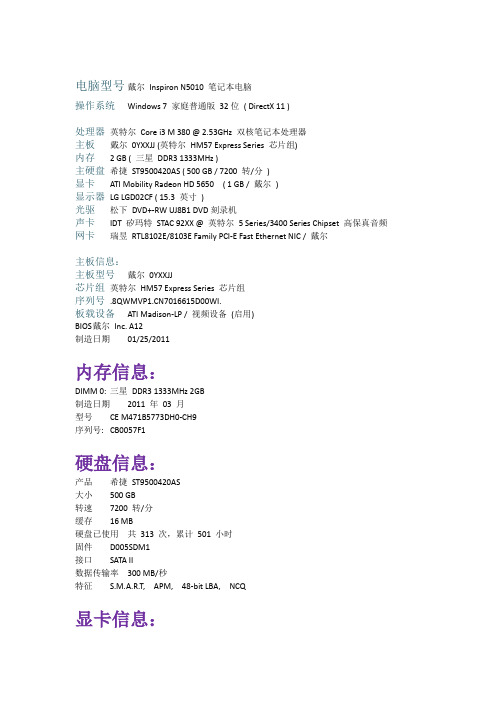
电脑型号戴尔Inspiron N5010 笔记本电脑操作系统Windows 7 家庭普通版32位( DirectX 11 )处理器英特尔Core i3 M 380 @ 2.53GHz 双核笔记本处理器主板戴尔0YXXJJ (英特尔HM57 Express Series 芯片组)内存 2 GB ( 三星DDR3 1333MHz )主硬盘希捷ST9500420AS ( 500 GB / 7200 转/分)显卡ATI Mobility Radeon HD 5650 ( 1 GB / 戴尔)显示器LG LGD02CF ( 15.3 英寸)光驱松下DVD+-RW UJ8B1 DVD刻录机声卡IDT 矽玛特STAC 92XX @ 英特尔5 Series/3400 Series Chipset 高保真音频网卡瑞昱RTL8102E/8103E Family PCI-E Fast Ethernet NIC / 戴尔主板信息:主板型号戴尔0YXXJJ芯片组英特尔HM57 Express Series 芯片组序列号7016615D00WI.板载设备ATI Madison-LP / 视频设备(启用)BIOS 戴尔Inc. A12制造日期01/25/2011内存信息:DIMM 0: 三星DDR3 1333MHz 2GB制造日期2011 年03 月型号CE M471B5773DH0-CH9序列号: CB0057F1硬盘信息:产品希捷ST9500420AS大小500 GB转速7200 转/分缓存16 MB硬盘已使用共313 次,累计501 小时固件D005SDM1接口SATA II数据传输率300 MB/秒特征S.M.A.R.T, APM, 48-bit LBA, NCQ显卡信息:主显卡ATI Mobility Radeon HD 5650显存 1 GB频率核心: 450MHz / 显存: 800MHz制造商戴尔BIOS版本BR39621.001BIOS日期01/04/11驱动版本8.783.3.0驱动日期1-28-2011光驱信息:产品松下DVD+-RW UJ8B1 DVD刻录机缓存/固件: 1536 KB / D.04网卡信息:网卡瑞昱RTL8102E/8103E Family PCI-E Fast Ethernet NIC制造商戴尔无线网卡英特尔Wireless WiFi Link 100 Series声卡信息:声卡IDT 矽玛特STAC 92XX @ 英特尔5 Series/3400 Series Chipset HD Audio声卡IDT 矽玛特STAC 92XX @ ATI Radeon HD 5600 Redwood HDMI Audio Device电池信息:产品SMP DELL 8NH5514 - 12068 锂电池电池损耗13.48%完全充电容量42258 mWh出厂设计容量48840 mWhID 12068SMPDELL 8NH5514处理器信息:处理器英特尔Core i3 M 380 @ 2.53GHz 双核笔记本处理器速度 2.53 GHz (133 MHz x 19.0)处理器数量核心数: 2 / 线程数: 4核心代号Arrandale生产工艺32 纳米插槽/插座Socket uPGA-989一级数据缓存 2 x 32 KB, 8-Way, 64 byte lines一级代码缓存 2 x 32 KB, 4-Way, 64 byte lines二级缓存 2 x 256 KB, 8-Way, 64 byte lines三级缓存 3 MB, 12-Way, 64 byte lines特征MMX, SSE, SSE2, SSE3, SSSE3, SSE4.1, SSE4.2, HTT, EM64T, EIST显示器信息:产品LG LGD02CF制造日期2010 年屏幕尺寸15.3 英寸(34 厘米x 19 厘米)显示比例宽屏16 : 9分辨率1366 x 768 32 位真彩色最大分辨率1366 x 768。
5510说明书

(2)起升机构工作前,应通电空载检查,调整制动片与制动轮之间的间隙,再满负荷调整,通电后间隙调整在0.5-1mm之间为宜。
(3)使用前,应检查减速器的油量是否合适,油质是否符合要求,否则必须添加或更换润滑油。
牵引机构
速度
电机型号
功率
转速
40.5/20m/min
YDEJ132S-4/8
3.3/2.2KW
710/1440 r/min
顶升机构
速度
电机型号
功率
转速
工作压力
0.7m/min
Y132S-4
5.5KW
1440 r/min
20MPa
平衡重
臂长55米
14.5t 用七块 2.2t×6+1.3t
臂长50米
13.2t用六块 2.2t×6
6.3、各种安全装置的调整……………………………………………………51
七、塔机的使用与维护保养…………………………………………………56
7.1、塔机的安全使用须知……………………………………………………56
7.2、塔机的维护保养…………………………………………………………57
7.3、塔机的工作条件和工作环境……………………………………………59
3.2、套架………………………………………………………………………15
3.3、回转支承座………………………………………………………………15
3.4、回转塔身节………………………………………………………………16
3.5、司机室……………………………………………………………………16
3.6、塔帽………………………………………………………………………16
CF5010DN1中文资料
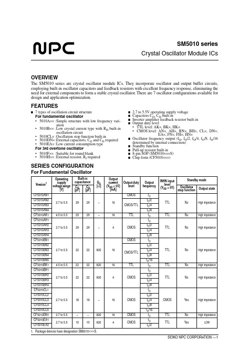
SM5010 seriesCrystal Oscillator Module ICs OVERVIEWThe SM5010 series are crystal oscillator module ICs. They incorporate oscillator and output buffer circuits, employing built-in oscillator capacitors and feedback resistors with excellent frequency response, eliminating the need for external components to form a stable crystal oscillator. There are 7 oscillator configurations available for design and application optimization.FEATURESI7 types of oscillation circuit structureFor fundamental oscillator•5010A××:Simple structure with low frequency vari-ation•5010B××:Low crystal current type with R D built-inoscillation circuit•5010CL×:Oscillation stop function built-in •5010DN×:External capacitors, C G and C D required •5010EA×:Low current consumption typeFor 3rd overtone oscillator•5010F××:Suitable for round blank•5010H××:External resistor, R f required I 2.7 to 5.5V operating supply voltageI Capacitors C G, C D built-inI Inverter amplifier feedback resistor built-inI Output duty level•TTL level: AK×, BK×, HKוCMOS level:AN×, AH×, BN×, BH×, CL×, DN×,EA×, FN×, FH×, HN×I Oscillator frequency output (f O, f O/2, f O/4, f O/8, f O/16determined by internal connection)I Standby functionI Pull-up resistor built-inI8-pin SOP (SM5010×××S)I Chip form (CF5010×××)SERIES CONFIGURATION For Fundamental OscillatorVersion1Operatingsupplyvoltage range[V]Built-incapacitance RD[Ω]Outputcurrent(V DD = 5V)[mA]Output dutylevelOutputfrequencyINHN inputlevel(V DD = 5V)Standby modeC G[pF]C D[pF]Oscillatorstop function Output stateCF5010AN12.7 to 5.52929–16CMOS f OTTL No High impedanceCF5010AN2CMOS/TTL f O/2CF5010AN3f O/4CF5010AN4f O/8CF5010AK1 4.5 to 5.52929–16TTL f O TTL No High impedanceCF5010AH12.7 to 5.52929–4CMOS f OTTL No High impedanceCF5010AH2f O/2 CF5010AH3f O/4 CF5010AH4f O/8CF5010BN12.7 to 5.5222282016CMOS f OTTL No High impedanceCF5010BN2CMOS/TTL f O/2CF5010BN3f O/4CF5010BN4f O/8CF5010BN5f O/16CF5010BK1 4.5 to 5.5222282016TTL f O TTL No High impedanceCF5010BH12.7 to 5.522228204CMOS f OTTL No High impedanceCF5010BH2f O/2 CF5010BH3f O/4 CF5010BH4f O/8CF5010CL12.7 to 5.51818–16CMOS f OCMOS Yes High impedanceCF5010CL2f O/2CF5010CL3f O/4CF5010CL4f O/8CF5010CL5f O/16CF5010DN1 2.7 to 5.5––82016CMOS f O TTL No High impedanceCF5010EA12.7 to 5.510158204CMOS f OTTL Yes LOWCF5010EA2f O/21. Package devices have designation SM5010×××S.元器件交易网SM5010 seriesSERIES CONFIGURATIONFor 3rd Overtone OscillatorORDERING INFORMATIONPACKAGE DIMENSIONS(Unit: mm) • 8-pin SOPVersion Operating supply voltage range [V]gm ratioBuilt-in capacitanceR f [k Ω ]Output current (V DD = 5V) [mA]Output duty levelC G [pF]CD [pF] CF5010FNA 2.7 to 5.51.001315 4.216CMOSCF5010FNC 1117 3.1CF5010FND 1317 2.2CF5010FNE 4.5 to 5.5815 2.2CF5010FHA 4.5 to 5.51.001315 4.24CMOSCF5010FHC 1117 3.1CF5010FHD 1317 2.2CF5010FHE 815 2.2CF5010HN1 4.5 to 5.5 1.17131720016CMOS CF5010HK14.5 to5.51.17131720016TTLDevice Package SM5010 ××× S 8-pin SOP CF5010 ×××–1Chip form元器件交易网SM5010 seriesPAD LAYOUT(Unit: µ m)PINOUT(Top view)PIN DESCRIPTION and PAD DIMENSIONSNumberNameI/ODescriptionPad dimensions [µm]X Y 1INHN I Output state control input. Standby mode when LOW, pull-up resistor built in. In the case of the 5010CL × , the oscillator stops and Power-saving pull-up resistor is built-in to reduce current consumption at standby mode.195174.42XT I Amplifier input.Crystal oscillator connection pins.Crystal oscillator connected between XT and XTN385174.43XTN O Amplifier output.575174.44VSS –Ground765174.45Q O Output. Output frequency (f O , f O /2, f O /4, f O /8, f O/16) determined by internal connection 757.61017.66NC –No connection ––7NC –No connection ––8VDD–Supply voltage165.41014.6元器件交易网元器件交易网SM5010 series BLOCK DIAGRAMFor Fundamental OscillatorI5010A××, B××, CL×, DN×, EA× seriesFor 3rd Overtone OscillatorI5010F××, H×× seriesSM5010 seriesFUNCTIONAL DESCRIPTIONStandby Function5010AH × , AK × , AN × , BH × , BK × , BN × , DN×, FN ×, FH ×, HN ×, HK × seriesWhen INHN goes LOW, the output on Q becomes high impedance, but internally the oscillator does not stop.5010CL × seriesWhen INHN goes LOW, the oscillator stops and the oscillator output on Q becomes high impedance.5010EA × seriesWhen INHN goes LOW, the oscillator stops and the oscillator output on Q becomes LOW.Power-saving Pull-up Resistor (CL series only)The INHN pull-up resistance changes in response to the input level (HIGH or LOW). When INHN goes LOW (standby state), the pull-up resistance becomes large to reduce the current consumption during standby.Version INHN QOscillator AH ×, AK ×, AN ×, BH ×, BK ×, BN ×, DN ×, FH ×, FH ×, HN ×, HK × seriesHIGH (or open)Any f O , f O /2, f O /4, f O /8 or f O /16 output frequencyNormal operation LOW High impedanceNormal operation CL × seriesHIGH (or open)Any f O , f O /2, f O /4, f O /8 or f O /16 output frequencyNormal operationLOW High impedanceStopped EA × seriesHIGH (or open)Either f O or f O /2 output frequencyNormal operationLOWLOWStopped元器件交易网SPECIFICATIONSAbsolute Maximum RatingsV SS = 0VRecommended Operating Conditions3V operation V SS = 0VParameterSymbol ConditionRating Unit Supply voltage range V DD −0.5 to +7.0V Input voltage range V IN −0.5 to V DD + 0.5V Output voltage range V OUT −0.5 to V DD + 0.5V Operating temperature range T opr −40 to +85°C Storage temperature rangeT stgChip form −65 to +150°C8-pin SOP−55 to +125Output currentI OUT AH ×, BH ×, FH ×, EA ×10mA AN ×, AK ×, BN ×, BK ×, CL ×, DN ×, FN ×, HN ×, HK ×25Power dissipation P D8-pin SOP500mWParameter Symbol Version ConditionRating Unit Operating supply voltage V DD All version 2.7 to 3.6V Input voltageV INAll version V SS to V DDVOperating temperatureT OPR5010AN ×−10 to +70°C5010AH ×5010BN ×5010BH ×5010CL ×−20 to +805010DN1−10 to +705010EA ×5010FN ×Operating frequencyf5010AN ×C L ≤ 15pF2 to 30MHz5010AH × 2 to 165010BN ×2 to 305010BH × 2 to 165010CL × 2 to 305010DN15010EA ×5010FN ×22 to 405V operationV SS = 0VParameter Symbol Version Condition Rating Unit Operating supply voltage V DD All version 4.5 to 5.5V Input voltage V IN All version V SS to V DD VOperating temperature T OPR 5010AN×−40 to +85°C 5010AK×5010AH×5010BN×5010BK×5010BH×5010CL×5010DN15010EA×C L≤ 15pF, f = 2 to 30MHzC L≤ 15pF, f = 2 to 40MHz−10 to +705010FN×C L≤ 50pF, 30MHz ≤ f ≤ 50MHz−20 to +80C L≤ 15pF, 50MHz ≤ f ≤ 70MHz−15 to +755010FH×C L≤ 15pF, 30MHz ≤ f ≤ 50MHz−20 to +80C L≤ 15pF, 50MHz ≤ f ≤ 60MHz−15 to +755010HN1−40 to +855010HK1Operating frequency f 5010AN×C L≤ 50pF2 to 30MHz 5010AK×C L≤ 15pF5010AH×5010BN×C L≤ 50pF5010BK×C L≤ 15pF5010BH×5010CL×C L≤ 50pF5010DN15010EA×C L≤ 15pF, Ta =− 40 to + 85°C 2 to 405010FN×C L≤ 50pF, Ta =− 20 to + 80°C30 to 50C L≤ 15pF, Ta =− 15 to + 75°C50 to 705010FH×C L≤ 15pF, Ta =− 20 to + 80°C30 to 50C L≤ 15pF, Ta =− 15 to + 75°C50 to 605010HN1C L≤ 50pF22 to 505010HK1C L≤ 15pFElectrical Characteristics5010AN ×, BN ×, DN × series3V operation: V DD = 2.7 to 3.6V , V SS = 0V , Ta = −10 to +70°C unless otherwise noted.5010AN ×, AK ×, BN ×, BK ×, DN × series5V operation: V DD = 4.5 to 5.5V , V SS = 0V , Ta = −40 to +85°C unless otherwise noted.Parameter Symbol ConditionRatingUnit min typ max HIGH-level output voltage V OH Q: Measurement cct 1, V DD = 2.7V, I OH = 8mA 2.1 2.4–V LOW-level output voltage V OL Q: Measurement cct 2, V DD = 2.7V, I OL = 8mA –0.30.4V HIGH-level input voltage V IH INHN 2.0––V LOW-level input voltage V IL INHN––0.5V Output leakage currentI ZQ: Measurement cct 2, INHN = LOW, V DD = 3.6VV OH = V DD ––10µAV OL = V SS ––10Current consumptionI DDMeasurement cct 3, load cct 1,INHN = open, C L = 15pF , f = 30MHz5010×N1–510mA 5010×N2– 3.575010×N3– 2.555010×N4–245010×N5–24INHN pull-up resistance R UP2Measurement cct 440100250k ΩFeedback resistance R f Measurement cct 580200500k ΩOscillator amplifier output resistanceR D Design value5010B ××690820940ΩBuilt-in capacitanceC GDesign value. A monitor pattern on a wafer is tested.5010A ××262932pF 5010B ××202224C D5010A ××2629325010B ××202224Parameter Symbol ConditionRatingUnit min typ max HIGH-level output voltage V OH Q: Measurement cct 1, V DD = 4.5V, I OH = 16mA 3.9 4.2–V LOW-level output voltage V OL Q: Measurement cct 2, V DD = 4.5V, I OL = 16mA –0.30.4V HIGH-level input voltage V IH INHN 2.0––V LOW-level input voltage V IL INHN––0.8V Output leakage currentI ZQ: Measurement cct 2, INHN = LOW, V DD = 5.5VV OH = V DD ––10µAV OL = V SS ––10Current consumptionI DDMeasurement cct 3, load cct 1, INHN = open, C L = 50pF , f = 30MHz5010×N1–1530mA 5010×N2–9185010×N3–6125010×N4–5105010×N5–510Measurement cct 3, load cct 2,INHN = open, C L = 15pF , f = 30MHz5010×K1–1020INHN pull-up resistance R UP2Measurement cct 440100250k ΩFeedback resistance R f Measurement cct 580200500k ΩOscillator amplifier output resistanceR D Design value5010B ××690820940ΩBuilt-in capacitanceC GDesign value. A monitor pattern on a wafer is tested.5010A ××262932pF 5010B ××202224C D5010A ××2629325010B ××2022245010AH ×, BH × series3V operation: V DD = 2.7 to 3.6V , V SS = 0V , Ta = −10 to +70°C unless otherwise noted.5V operation: V DD = 4.5 to 5.5V , V SS = 0V , Ta = −40 to +85°C unless otherwise noted.Parameter Symbol ConditionRatingUnit min typ max HIGH-level output voltage V OH Q: Measurement cct 1, V DD = 2.7V, I OH = 2mA 2.1 2.4–V LOW-level output voltage V OL Q: Measurement cct 2, V DD = 2.7V, I OL = 2mA –0.30.5V HIGH-level input voltage V IH INHN 2.0––V LOW-level input voltage V IL INHN––0.5V Output leakage currentI ZQ: Measurement cct 2, INHN = LOW, V DD = 3.6VV OH = V DD ––10µAV OL = V SS ––10Current consumptionI DDMeasurement cct 3, load cct 1,INHN = open, C L = 15pF , f = 16MHz5010×H1–36mA 5010×H2–245010×H3– 1.535010×H4– 1.5 2.5INHN pull-up resistance R UP2Measurement cct 440100250k ΩFeedback resistance R f Measurement cct 580200500k ΩOscillator amplifier output resistanceR D Design value5010B ××690820940ΩBuilt-in capacitanceC GDesign value. A monitor pattern on a wafer is tested.5010A ××262932pF 5010B ××202224C D5010A ××2629325010B ××202224Parameter Symbol ConditionRatingUnit min typ max HIGH-level output voltage V OH Q: Measurement cct 1, V DD = 4.5V, I OH = 4mA 3.9 4.2–V LOW-level output voltage V OL Q: Measurement cct 2, V DD = 4.5V, I OL = 4mA –0.30.5V HIGH-level input voltage V IH INHN 2.0––V LOW-level input voltage V IL INHN––0.8V Output leakage currentI ZQ: Measurement cct 2, INHN = LOW, V DD = 5.5VV OH = V DD ––10µAV OL = V SS ––10Current consumptionI DDMeasurement cct 3, load cct 1,INHN = open, C L = 15pF , f = 30MHz5010×H1–918mA 5010×H2–6125010×H3–5105010×H4–48INHN pull-up resistance R UP2Measurement cct 440100250k ΩFeedback resistance R f Measurement cct 580200500k ΩOscillator amplifier output resistanceR D Design value5010B ××690820940ΩBuilt-in capacitanceC GDesign value. A monitor pattern on a wafer is tested.5010A ××262932pF 5010B ××202224C D5010A ××2629325010B ××2022245010CL × series3V operation: V DD = 2.7 to 3.6V , V SS = 0V , Ta = −20 to +80°C unless otherwise noted.5V operation: V DD = 4.5 to 5.5V , V SS = 0V , Ta = −40 to +85°C unless otherwise noted.Parameter Symbol ConditionRatingUnit min typ max HIGH-level output voltage V OH Q: Measurement cct 1, V DD = 2.7V, I OH = 8mA 2.2 2.4–V LOW-level output voltage V OL Q: Measurement cct 2, V DD = 2.7V, I OL = 8mA –0.30.4V HIGH-level input voltage V IH INHN 0.7V DD ––V LOW-level input voltage V IL INHN––0.3V DD V Output leakage currentI ZQ: Measurement cct 2, INHN = LOW, V DD = 3.6VV OH = V DD ––10µAV OL = V SS ––10Current consumptionI DDMeasurement cct 3, load cct 1,INHN = open, C L = 15pF , f = 30MHz5010CL1–510mA 5010CL2– 3.575010CL3– 2.555010CL4–245010CL5–24Standby current I ST Measurement cct 6, INHN = LOW ––5µA INHN pull-up resistance R UP1Measurement cct 42415M ΩR UP240100250k ΩFeedback resistance R f Measurement cct 580200500k ΩBuilt-in capacitanceC G Design value. A monitor pattern on a wafer is tested.161820pF C D161820Parameter Symbol ConditionRatingUnit min typ max HIGH-level output voltage V OH Q: Measurement cct 1, V DD = 4.5V, I OH = 16mA 4.0 4.2–V LOW-level output voltage V OL Q: Measurement cct 2, V DD = 4.5V, I OL = 16mA –0.30.4V HIGH-level input voltage V IH INHN 0.7V DD ––V LOW-level input voltage V IL INHN––0.3V DD V Output leakage currentI ZQ: Measurement cct 2, INHN = LOW, V DD = 5.5VV OH = V DD ––10µAV OL = V SS ––10Current consumptionI DDMeasurement cct 3, load cct 1,INHN = open, C L = 50pF , f = 30MHz5010CL1–1530mA 5010CL2–9185010CL3–6125010CL4–5105010CL5–510Standby current I ST Measurement cct 6, INHN = LOW ––10µA INHN pull-up resistance R UP1Measurement cct 4128M ΩR UP240100250k ΩFeedback resistance R f Measurement cct 580200500k ΩBuilt-in capacitanceC G Design value. A monitor pattern on a wafer is tested.161820pF C D1618205010EA × series3V operation: V DD = 2.7 to 3.6V , V SS = 0V , Ta = −10 to +70°C unless otherwise noted.5V operation: V DD = 4.5 to 5.5V , V SS = 0V , Ta = −40 to +85°C unless otherwise noted.Parameter Symbol ConditionRatingUnit min typ max HIGH-level output voltage V OH Q: Measurement cct 1, V DD = 2.7V, I OH = 2mA 2.1 2.4–V LOW-level output voltage V OL Q: Measurement cct 2, V DD = 2.7V, I OL = 2mA –0.30.5V HIGH-level input voltage V IH INHN 2.0––V LOW-level input voltage V IL INHN––0.5V Current consumption I DD Measurement cct 3, load cct 1,INHN = open, C L = 15pF , f = 30MHz 5010EA1–48mA 5010EA2– 2.55INHN pull-up resistance R UP2Measurement cct 440100250k ΩFeedback resistance R f Measurement cct 580200500k ΩOscillator amplifier output resistance R D Design value690820940ΩBuilt-in capacitanceC G Design value. A monitor pattern on a wafer is tested.91011pFC D131517Parameter Symbol ConditionRatingUnit min typ max HIGH-level output voltage V OH Q: Measurement cct 1, V DD = 4.5V, I OH = 3.2mA 3.9 4.2–V LOW-level output voltage V OL Q: Measurement cct 2, V DD = 4.5V, I OL = 3.2mA –0.30.4V HIGH-level input voltage V IH INHN 2.0––V LOW-level input voltageV IL INHN––0.8VCurrent consumptionI DD1Measurement cct 3, load cct 1,INHN = open, C L = 15pF , f = 30MHz5010EA1–612mA 5010EA2–510I DD2Measurement cct 3, load cct 1,INHN = open, C L = 15pF , f = 40MHz 5010EA1–9185010EA2–612INHN pull-up resistance R UP2Measurement cct 440100250k ΩFeedback resistance R f Measurement cct 580200500k ΩOscillator amplifier output resistance R D Design value690820940ΩBuilt-in capacitanceC G Design value. A monitor pattern on a wafer is tested.91011pFC D1315175010FN× series3V operation: V DD = 2.7 to 3.6V, V SS = 0V, Ta = −10 to +70°C unless otherwise noted.Parameter Symbol ConditionRatingUnit min typ maxHIGH-level output voltage V OH Q: Measurement cct 1, V DD = 2.7V, I OH = 8mA 2.2 2.4–V LOW-level output voltage V OL Q: Measurement cct 2, V DD = 2.7V, I OL = 8mA–0.30.4V HIGH-level input voltage V IH INHN 2.0––V LOW-level input voltage V IL INHN––0.5VOutput leakage current I Z Q: Measurement cct 2, INHN = LOW,V DD = 3.6VV OH = V DD––10µAV OL = V SS––10Current consumption I DD Measurement cct 3, load cct 1,INHN = open, C L = 15pF5010FNA, FNCf = 30MHz–816mA5010FNDf = 40MHz–1020INHN pull-up resistance R UP Measurement cct 440100250kΩFeedback resistance R f Measurement cct 55010FNA 3.57 4.2 4.83kΩ5010FNC 2.63 3.1 3.575010FND 1.87 2.2 2.53Built-in capacitance C GDesign value. A monitor pattern on awafer is tested.5010FNA11.71314.3pF5010FNC9.91112.15010FND11.71314.3C D5010FNA13.51516.55010FNC15.31718.75010FND15.31718.75V operation:V DD = 4.5 to 5.5V, V SS = 0V30 ≤ f ≤ 50MHz: Ta = −20 to +80°C, 50 < f ≤ 70MHz: Ta = −15 to +75°C unless otherwise noted.Parameter Symbol ConditionRatingUnit min typ maxHIGH-level output voltage V OH Q: Measurement cct 1, V DD = 4.5V, I OH = 16mA 3.9 4.2–V LOW-level output voltage V OL Q: Measurement cct 2, V DD = 4.5V, I OL = 16mA–0.30.4V HIGH-level input voltage V IH INHN 2.0––V LOW-level input voltage V IL INHN––0.8VOutput leakage current I Z Q: Measurement cct 2, INHN = LOW,V DD = 5.5VV OH = V DD––10µAV OL = V SS––10Current consumption I DD1Measurement cct 3, load cct 1,INHN = open, C L = 15pF5010FNEf = 70MHz–2550mA I DD2Measurement cct 3, load cct 1,INHN = open, C L = 50pF5010FNA, FNCf = 40MHz–23455010FNDf = 50MHz–2550INHN pull-up resistance R UP Measurement cct 440100250kΩFeedback resistance R f Measurement cct 55010FNA 3.57 4.2 4.83kΩ5010FNC 2.63 3.1 3.575010FND 1.87 2.2 2.535010FNE 1.87 2.2 2.53Built-in capacitance C GDesign value. A monitor pattern on awafer is tested.5010FNA11.71314.3pF5010FNC9.91112.15010FND11.71314.35010FNE7.288.8C D5010FNA13.51516.55010FNC15.31718.75010FND15.31718.75010FNE13.51516.55010FH × series5V operation:V DD = 4.5 to 5.5V , V SS = 0V30 ≤ f ≤ 50MHz: Ta = −20 to +80°C, 50 < f ≤ 60MHz: Ta = −15 to +75°C unless otherwise noted.5010HN ×, HK × series5V operation: V DD = 4.5 to 5.5V , V SS = 0V , Ta = −40 to +85°C unless otherwise noted.Parameter Symbol ConditionRatingUnit min typ max HIGH-level output voltage V OH Q: Measurement cct 1, V DD = 4.5V, I OH = 4mA 3.9 4.2–V LOW-level output voltage V OL Q: Measurement cct 2, V DD = 4.5V, I OL = 4mA –0.30.5V HIGH-level input voltage V IH INHN 2.0––V LOW-level input voltage V IL INHN––0.8V Output leakage currentI ZQ: Measurement cct 2, INHN = LOW, V DD = 5.5VV OH = V DD ––10µAV OL = V SS ––10Current consumptionI DDMeasurement cct 3, load cct 1,INHN = open, C L = 15pF5010FHA, FHC f = 40MHz–1326mA 5010FHD f = 50MHz –15305010FHE f = 60MHz–1734INHN pull-up resistanceR UPMeasurement cct 440100250k ΩFeedback resistanceR fMeasurement cct 55010FHA3.574.2 4.83k Ω5010FHC 2.63 3.1 3.575010FHD 1.87 2.2 2.535010FHE 1.87 2.2 2.53Built-in capacitanceC GDesign value. A monitor pattern on a wafer is tested.5010FHA11.71314.3pF 5010FHC 9.91112.15010FHD 11.71314.35010FHE 7.288.8C D5010FHA 13.51516.55010FHC 15.31718.75010FHD 15.31718.75010FHE13.51516.5Parameter Symbol ConditionRatingUnit min typ max HIGH-level output voltage V OH Q: Measurement cct 1, V DD = 4.5V, I OH = 16mA 3.9 4.2–V LOW-level output voltage V OL Q: Measurement cct 2, V DD = 4.5V, I OL = 16mA –0.30.4V HIGH-level input voltage V IH INHN 2.0––V LOW-level input voltage V IL INHN––0.8V Output leakage currentI Z Q: Measurement cct 2, INHN = LOW, V DD = 5.5VV OH = V DD ––10µAV OL = V SS ––10Current consumptionI DD1Measurement cct 3, load cct 2,INHN = open, C L = 15pF , f = 50MHz 5010HK1–2040mAI DD2Measurement cct 3, load cct 1,INHN = open, C L = 50pF , f = 50MHz 5010HN1–2550INHN pull-up resistance R UP Measurement cct 440100250k ΩFeedback resistance R f Measurement cct 580200500k ΩBuilt-in capacitanceC G Design value. A monitor pattern on a wafer is tested.11.71314.3pF C D15.31718.7Switching Characteristics5010AN ×, BN ×, DN × series3V operation/Duty level: CMOSV DD = 2.7 to 3.6V , V SS = 0V , Ta = −10 to +70°C unless otherwise noted.5010AN ×, AK ×, BN ×, BK ×, DN × series5V operation/Duty level: CMOS (5010AN ×, BN ×, DN1)V DD = 4.5 to 5.5V , V SS = 0V , Ta = −40 to +85°C unless otherwise noted.5V operation/Duty level: TTL (5010×K1, AN2, AN3, AN4, BN2, BN3, BN4, BN5)V DD = 4.5 to 5.5V , V SS = 0V , Ta = −40 to +85°C unless otherwise noted.Parameter Symbol ConditionRatingUnit min typ max Output rise time t r1Measurement cct 6, load cct 1, C L = 15pF , 0.1V DD to 0.9V DD – 3.0 6.0ns Output fall time t f1Measurement cct 6, load cct 1, C L = 15pF , 0.9V DD to 0.1V DD – 3.0 6.0ns Output duty cycle 11. The duty cycle characteristic is checked the sample chips of each production lot.Duty Measurement cct 6, load cct 1, V DD = 3.0V, Ta = 25°C, C L = 15pF , f = 30MHz40–60%Output disable delay time t PLZ Measurement cct 7, load cct 1, V DD = 3.0V, Ta = 25°C, C L = 15pF––100ns Output enable delay timet PZL––100nsParameterSymbol ConditionRatingUnitmin typ max Output rise time t r1Measurement cct 6, load cct 1, 0.1V DD to 0.9V DDC L = 15pF – 2.0 4.0nst r2C L = 50pF – 4.08.0Output fall time t f1Measurement cct 6, load cct 1, 0.9V DD to 0.1V DDC L = 15pF – 2.0 4.0nst f2C L = 50pF– 4.08.0Output duty cycle 11. The duty cycle characteristic is checked the sample chips of each production lot.Duty Measurement cct 6, load cct 1, V DD = 5.0V, Ta = 25°C, C L = 50pF , f = 30MHz45–55%Output disable delay time t PLZ Measurement cct 7, load cct 1, V DD = 5.0V, Ta = 25°C, C L = 15pF––100ns Output enable delay timet PZL––100nsParameter Symbol ConditionRatingUnit min typ max Output rise time t r3Measurement cct 6, load cct 2, C L = 15pF , 0.4V to 2.4V – 1.5 3.0ns Output fall time t f3Measurement cct 6, load cct 2, C L = 15pF , 2.4V to 0.4V – 1.5 3.0ns Output duty cycle 11. The duty cycle characteristic is checked the sample chips of each production lot.Duty Measurement cct 6, load cct 2, V DD = 5.0V, Ta = 25°C, C L = 15pF , f = 30MHz45–55%Output disable delay time t PLZ Measurement cct 7, load cct 2, V DD = 5.0V, Ta = 25°C, C L = 15pF––100ns Output enable delay timet PZL––100ns5010AH ×, BH × series3V operation/Duty level: CMOSV DD = 2.7 to 3.6V , V SS = 0V , Ta = −10 to +70°C unless otherwise noted.5V operation/Duty level: CMOSV DD = 4.5 to 5.5V , V SS = 0V , Ta = −40 to +85°C unless otherwise noted.Parameter Symbol ConditionRatingUnit min typ max Output rise time t r1Measurement cct 6, load cct 1, C L = 15pF , 0.1V DD to 0.9V DD –816ns Output fall time t f1Measurement cct 6, load cct 1, C L = 15pF , 0.9V DD to 0.1V DD –816ns Output duty cycle 11. The duty cycle characteristic is checked the sample chips of each production lot.Duty Measurement cct 6, load cct 1, V DD = 3.0V, Ta = 25°C, C L = 15pF , f = 16MHz40–60%Output disable delay time t PLZ Measurement cct 7, load cct 1, V DD = 3.0V, Ta = 25°C, C L = 15pF––100ns Output enable delay timet PZL––100nsParameterSymbol ConditionRatingUnitmin typ max Output rise time t r1Measurement cct 6, load cct 1, 0.1V DD to 0.9V DDC L = 15pF –510nst r2C L = 50pF –1326Output fall time t f1Measurement cct 6, load cct 1, 0.9V DD to 0.1V DDC L = 15pF –510nst f2C L = 50pF–1326Output duty cycle 11. The duty cycle characteristic is checked the sample chips of each production lot.Duty Measurement cct 6, load cct 1, V DD = 5.0V, Ta = 25°C, C L = 15pF , f = 30MHz45–55%Output disable delay time t PLZ Measurement cct 7, load cct 1, V DD = 5.0V, Ta = 25°C, C L = 15pF––100ns Output enable delay timet PZL––100ns5010CL × series3V operation/Duty level: CMOSV DD = 2.7 to 3.6V , V SS = 0V , Ta = −20 to +80°C unless otherwise noted.5V operation/Duty level: CMOSV DD = 4.5 to 5.5V , V SS = 0V , Ta = −40 to +85°C unless otherwise noted.ParameterSymbol ConditionRatingUnitmin typ max Output rise time t r1Measurement cct 6, load cct 1, 0.1V DD to 0.9V DDC L = 15pF – 2.0 4.0nst r4C L = 30pF – 3.0 6.0Output fall time t f1Measurement cct 6, load cct 1, 0.9V DD to 0.1V DDC L = 15pF – 2.0 4.0nst f4C L = 30pF– 3.0 6.0Output duty cycle 11. The duty cycle characteristic is checked the sample chips of each production lot.Duty Measurement cct 6, load cct 1, V DD = 3.0V, Ta = 25°C, C L = 15pF , f = 30MHz45–55%Output disable delay time 22. Oscillator stop function is built-in. When INHN goes LOW, normal output stops. When INHN goes HIGH, normal output is not resumed until after the oscillator start-up time has elapsed.t PLZ Measurement cct 7, load cct 1, V DD = 3.0V, Ta = 25°C, C L = 15pF––100ns Output enable delay time 2t PZL––100nsParameterSymbol ConditionRatingUnitmin typ max Output rise time t r1Measurement cct 6, load cct 1, 0.1V DD to 0.9V DDC L = 15pF – 1.5 3.0nst r2C L = 50pF – 4.08.0Output fall time t f1Measurement cct 6, load cct 1, 0.9V DD to 0.1V DDC L = 15pF – 1.5 3.0nst f2C L = 50pF– 4.08.0Output duty cycle 11. The duty cycle characteristic is checked the sample chips of each production lot.Duty Measurement cct 6, load cct 1, V DD = 5.0V, Ta = 25°C, C L = 50pF , f = 30MHz40–60%Output disable delay time 22. Oscillator stop function is built-in. When INHN goes LOW, normal output stops. When INHN goes HIGH, normal output is not resumed until after the oscillator start-up time has elapsed.t PLZ Measurement cct 7, load cct 1, V DD = 5.0V, Ta = 25°C, C L = 15pF––100ns Output enable delay time 2t PZL––100ns5010EA × series3V operation/Duty level: CMOSV DD = 2.7 to 3.6V , V SS = 0V , Ta = −10 to +70°C unless otherwise noted.5V operation/Duty level: CMOSV DD = 4.5 to 5.5V , V SS = 0V , Ta = −40 to +85°C unless otherwise noted.Parameter Symbol ConditionRatingUnit min typ max Output rise time t r1Measurement cct 6, load cct 1, C L = 15pF , 0.1V DD to 0.9V DD –816ns Output fall time t f1Measurement cct 6, load cct 1, C L = 15pF , 0.9V DD to 0.1V DD –816ns Output duty cycle 11. The duty cycle characteristic is checked the sample chips of each production lot.Duty Measurement cct 6, load cct 1, V DD = 3.0V, Ta = 25°C, C L = 15pF , f = 30MHz40–60%Output disable delay time 22. Oscillator stop function is built-in. When INHN goes LOW, normal output stops. When INHN goes HIGH, normal output is not resumed until after the oscillator start-up time has elapsed.t PLZ Measurement cct 7, load cct 1, V DD = 3.0V, Ta = 25°C, C L = 15pF––100ns Output enable delay time 2t PZL––100nsParameterSymbol ConditionRatingUnitmin typ max Output rise time t r1Measurement cct 6, load cct 1, 0.1V DD to 0.9V DDC L = 15pF –510nst r2C L = 50pF –1326Output fall time t f1Measurement cct 6, load cct 1, 0.9V DD to 0.1V DDC L = 15pF –510nst f2C L = 50pF –1326Output duty cycle 11. The duty cycle characteristic is checked the sample chips of each production lot.Duty1Measurement cct 6, load cct 1, V DD = 5.0V, Ta = 25°C, C L = 15pFf = 30MHz 45–55%Duty2 f = 40MHz40–60Output disable delay time 22. Oscillator stop function is built-in. When INHN goes LOW, normal output stops. When INHN goes HIGH, normal output is not resumed until after the oscillator start-up time has elapsed.t PLZ Measurement cct 7, load cct 1, V DD = 5.0V, Ta = 25°C, C L = 15pF––100ns Output enable delay time 2t PZL––100ns。
SDM3055数字万用表数据手册-2017.06说明书
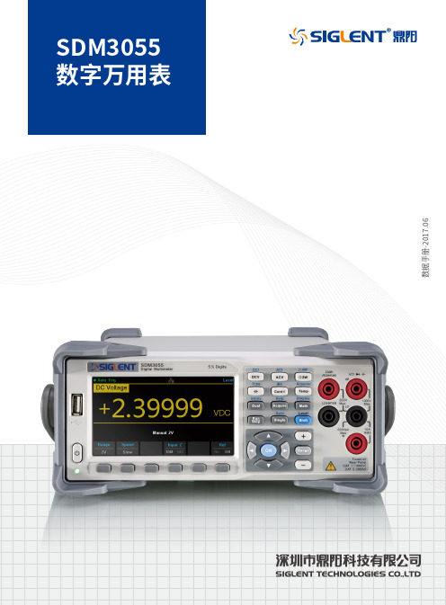
SDM3055数字万用表数据手册-2017.06SDM3055 数字万用表产品综述S DM3055 5½位双显示数字万用表,拥有出众的测量精度,是一款针对高精度、多功能、自动测量的用户需求而设计的产品。
产品功能基本测量功能•直流电压测量:200 mV ,2V,20V,200V,1000 V •直流电流测量:200 μA,2mA,20mA,200mA, 2A,10A•交流电压测量:True-RMS,200 mV,2V,20V,200V,750V •交流电流测量:True-RMS,20 mA ,200mA,2A, 10 A•2、4线电阻测量:200 Ω,2K,20K,200K,2M, 10M,100MΩ•电容测量:2 nF,20nF,200nF,2μF,20μF,200μF,10000 μF• 连通性测试:量程固定在2KΩ •二极管测试:0~4阀值可调• 频率测量:20 Hz ~ 1MHz • 周期测量:1 μs ~ 0.05 s•温度测量:支持热电偶,热电阻温度传感器 数学运算功能•最大值、最小值、平均值、标准差、相对测量、条形 表,直方图,趋势图,dB/dBm,限值等主要特色• 4.3英寸真彩TFT-LCD 大屏显示,分辨率480*272 •真正的5½位读数分辨率 (240,000 count) • 高达150 rdgs/s 的测量速度 • 真有效值交流电压和交流电流测量•1 Gb Nand Flash 总容量,海量存储仪器设置文件和数 据文件• 内置热电偶冷端补偿• 支持标准SCPI 远程控制命令、上位机软件、兼容最新 主流万用表命令集 • 支持双显示、中英文菜单 • 内置帮助系统,方便信息获取• 配置接口:USB Device,USB Host,LAN •选购配件: USB-GPIB 适配器,扫描卡SC1016•设置和测量数据可通过VXI11,USBTMC, U 盘导入或者导出以方便用户修改,查看,备份应用领域•科研教育 •研发机构 •检测维修•校准•自动化生产测试人性化设计图形化的用户界面,操作简单方便。
M5000 其它材料 M5110 用于制造1、2、3级设备中螺钉类紧固件和驱动杆的轧制或锻造棒材
X
X
不锈钢 Z6CND17.12
X
X
Z5CND17.12
X
X
特殊牌号
不锈钢:
—马氏体 Z12CNDV12.02(1) X
X
—马氏体 Z6CNU17.04(3) X
X
时效硬化 Z6CNUD15.04(3) X
X
—奥氏体 Z6NCTDV25.15 X
X
X
时效硬化
(1)根据要求的断裂吸收能,此钢号只适用与 2、3 级设备。
和 Smax/Smin≤1.25
按 MC1000 规定进行硬度试验。每批的每根棒材都须测定硬度值。 首先,硬度试验可以评定棒材的均匀性,其次,它允许选择试验用超长部分。 a)以热处理状态交货的棒材: 所得硬度值应符合 4.1 的要求。 b)以制造状态交货的棒材或在以后加工中需经热处理改变其力学性能的棒 材: 在经模拟热处理的试料上所测得的硬度值应符合 4.1 的要求。 4.2.3 试验用超长部分 试料应取自棒材的超长部分。截取应在所有热处理完成之后进行。 超长部分必须取自: ——非加工硬化的棒材: 每根棒材进行硬度测量后,在每批中取 4%(至少为 2 根)的棒材进行试验, 其中 2%为该批中硬度最高的棒材,另外 2%为该批中硬度最低的棒材; ——经加工硬化的奥氏体不锈钢棒材: 若逐棒进行冷加工,则试验在每根棒上进行; 若该批是取自单次操作的轧制的、未轧制的和冷加工的棒材顶部,则试验在 该批的一根棒材上进行。 试料要具有足够的尺寸,以便截取全部试验和复试所需用的试样。 4.2.4 取样 试样应按以下规定截取: ——试样轴线应与棒材轴线平行,其轴线与表面的距离规定为: Φ≤25mm 时,在棒材轴线处; 25mm<Φ≤50mm 时,离表面 12.5mm 处; Φ>50mm 时,位于二分之一半径处; ——试验用试样的有用部分与棒料端部的距离不小于棒材直径。 对于热处理状态交货的棒料,用取自试料的试样进行试验,该试料取样后不 经任何热处理。 对于以制造状态交货的棒材或在以后加工中需经热处理以提高其力学性能的 棒材,试验应在经过模拟热处理的试料上进行。