INA333中文资料
IR333C中文资料

元器件交易网Technical Data Sheet 5mm Infrared LED , T-1 3/4IR333C/H0/L10Features․High reliability ․High radiant intensity ․Peak wavelength λp=940nm ․2.54mm Lead spacing ․Low forward voltage ․Pb free ․The product itself will remain within RoHS compliant version.Descriptions․EVERLIGHT’S Infrared Emitting Diode(IR333C/H0/L10) is a high intensity diode , molded in a water clear plastic package. ․The device is spectrally matched with phototransistor , photodiode and infrared receiver module.Applications․Free air transmission system ․Infrared remote control units with high power requirement ․Smoke detector ․Infrared applied systemDevice Selection Guide LED Part No.IRChip MaterialGaAlAsLens ColorWater clearEverlight Electronics Co., Ltd. Device No:DIR-033-087http:\\ Prepared date:07-20-2005Rev 3Page: 1 of 7Prepared by:Jaine Tsai元器件交易网IR333C/H0/L10Package DimensionsNotes: 1.All dimensions are in millimeters 2.Tolerances unless dimensions ±0.25mmAbsolute Maximum Ratings (Ta=25℃)Parameter Continuous Forward Current Peak Forward Current Reverse Voltage Operating Temperature Storage Temperature Soldering Temperature Power Dissipation at(or below) 25℃Free Air Temperature Symbol IF IFP VR Topr Tstg Tsol Pd Rating 100 1.0 5 -40 ~ +85 -40 ~ +85 260 150 Units mA A V ℃ ℃ ℃ mWNotes: *1:IFP Conditions--Pulse Width≦100μs and Duty≦1%. *2:Soldering time≦5 seconds.Everlight Electronics Co., Ltd. Device No:DIR-033-087http:\\ Prepared date:07-20-2005Rev 3Page: 2 of 7Prepared by:Jaine Tsai元器件交易网IR333C/H0/L10Electro-Optical Characteristics (Ta=25℃)Parameter Symbol Condition IF=20mA IF=100mA Radiant Intensity EePulse Width≦100μs ,Duty≦1%Min. 7.8 -----Typ. 10 45 450 940 45 1.2Max. -----1.5 1.8 4.0 10 --UnitsmW/srIF=1APulse Width≦100μs ,Duty≦1%.Peak Wavelength Spectral Bandwidthλp ΔλIF=20mA IF=20mA IF=20mA IF=100mAnm nmForward VoltageVFPulse Width≦100μs ,Duty≦1%-----1.4 2.6 -40VIF=1APulse Width≦100μs ,Duty≦1%.Reverse Current View AngleIR 2θ1/2VR=5V IF=20mAμA degRankCondition:IF=20mA Unit:mW/sr Bin Number Min Max M 7.80 12.5 N 11.0 17.6Everlight Electronics Co., Ltd. Device No:DIR-033-087http:\\ Prepared date:07-20-2005Rev 3Page: 3 of 7Prepared by:Jaine Tsai元器件交易网IR333C/H0/L10Typical Electro-Optical Characteristics CurvesFig.1 Forward Current vs. Ambient Temperature140 120Fig.2 Spectral Distribution100 80IF=20mA Ta=25° C100 80 60 40 20060 40 20 0-40 -20 020406080100Fig.3 Peak Emission Wavelength Ambient Temperature980Fig.4 Forward Current vs. Forward Voltage4 109603 109402 10920900 -251 100 25 50 75 10001234Everlight Electronics Co., Ltd. Device No:DIR-033-087http:\\ Prepared date:07-20-2005Rev 3Page: 4 of 7Prepared by:Jaine Tsai元器件交易网IR333C/H0/L10Typical Electro-Optical Characteristics CurvesFig.5 Relative Intensity vs. Forward Current Fig.6 Relative Radiant Intensity vs. Angular Displacement1000Ie-Radiant Intensity(mW/sr)-20-1001020 301001.0 0.940 50 60 70 80 0.6 0.4 0.2 0 0.2 0.4 0.6100.8 0.70 1 2 3 401010101010IF-Forward Current (mA)Fig.7 Relative Intensity vs. Ambient Temperature(°C)Fig.8 Forward Voltage vs. Ambient Temperature(°C)151.310IF=20mA1.2IF=20mA51.10 25 50 75 100 120125 50 75 100 120Everlight Electronics Co., Ltd. Device No:DIR-033-087http:\\ Prepared date:07-20-2005Rev 3Page: 5 of 7Prepared by:Jaine Tsai元器件交易网IR333C/H0/L10Reliability Test Item And ConditionThe reliability of products shall be satisfied with items listed below. Confidence level:90% LTPD:10% NO. Item Test Conditions Test Hours/ Sample Cycles Sizes 10secs 22pcs IR≧U×2 Ee≦L×0.8 VF≧U×1.2 U:Upper 1000hrs 1000hrs 1000hrs 1000hrs 22pcs 22pcs 22pcs 22pcs Specification Limit L:Lower Specification Limit 0/1 0/1 0/1 0/1 Failure Judgement Criteria Ac/Re1 Solder HeatTEMP.:260℃±5℃ 15mins 5mins 15mins 5mins 10secs 5mins0/1 0/12 Temperature Cycle H : +100℃ L : -40℃ 3 Thermal Shock H :+100℃ L :-10℃ 4 High Temperature Storage 5 Low Temperature Storage300Cycles 22pcs300Cycles 22pcs0/1TEMP.:+100℃ TEMP.:-40℃6 DC Operating Life IF=20mA 7 High Temperature/ 85℃ / 85% R.H High HumidityEverlight Electronics Co., Ltd. Device No:DIR-033-087http:\\ Prepared date:07-20-2005Rev 3Page: 6 of 7Prepared by:Jaine Tsai元器件交易网IR333C/H0/L10Packing Quantity Specification1.500PCS/1Bag,5Bags/1Box 2.10Boxes/1CartonLabel Form SpecificationCPN: Customer’s Production Number P/N : Production Number QTY: Packing Quantity AT: Ranks HUE: Peak Wavelength REF: Reference LOT No: Lot Number MADE IN TAIWAN: Production PlaceRoHSIR333C/H0/L10Notes1. Above specification may be changed without notice. EVERLIGHT will reserve authority on material change for above specification. 2. When using this product, please observe the absolute maximum ratings and the instructions for using outlined in these specification sheets. EVERLIGHT assumes no responsibility for any damage resulting from use of the product which does not comply with the absolute maximum ratings and the instructions included in these specification sheets. 3. These specification sheets include materials protected under copyright of EVERLIGHT corporation. Please don’t reproduce or cause anyone to reproduce them without EVERLIGHT’s consent.EVERLIGHT ELECTRONICS CO., LTD. Office: No 25, Lane 76, Sec 3, Chung Yang Rd, Tucheng, Taipei 236, Taiwan, R.O.CTel: 886-2-2267-2000, 2267-9936 Fax: 886-2267-6244, 2267-6189, 2267-6306 http:\\Everlight Electronics Co., Ltd. Device No:DIR-033-087http:\\ Prepared date:07-20-2005Rev 3Page: 7 of 7Prepared by:Jaine Tsai。
INA131中文资料
®
INA131
INA131
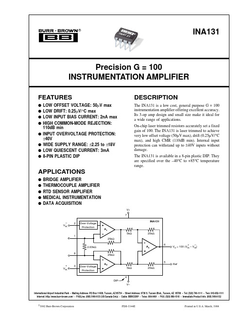
Precision G = 100 INSTRUMENTATION AMPLIFIER
FEATURES
q LOW OFFSET VOLTAGE: 50µV max q LOW DRIFT: 0.25µV/°C max q LOW INPUT BIAS CURRENT: 2nA max q HIGH COMMON-MODE REJECTION:
pA/√Hz
T
pA/√Hz
T
pAp-p
T
±0.1
%
T
T
%
T
±20
ppm/°C
T
±0.004 % of FSR
T
T
V
T
T
V
T
T
V
T
pF
T
mA
T
T
T
T
T
kHz V/µs µs µs
T
T
T
V
T
T
mA
T
T
°C
T
T
°C
T
°C/W
The information provided herein is believed to be reliable; however, BURR-BROWN assumes no responsibility for inaccuracies or omissions. BURR-BROWN assumes no responsibility for the use of this information, and all use of such information shall be entirely at the user’s own risk. Prices and specifications are subject to change without notice. No patent rights or licenses to any of the circuits described herein are implied or granted to any third party. BURR-BROWN does not authorize or warrant any BURR-BROWN product for use in life support devices and/or systems.
INA138中文资料

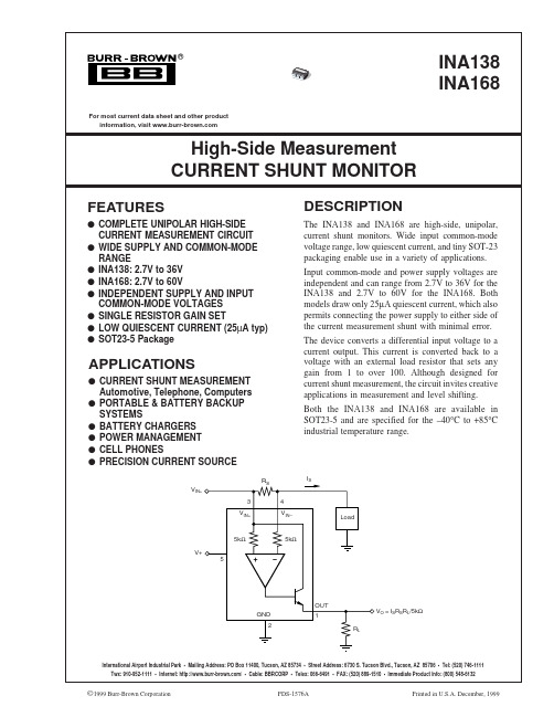
V+ 5
GND 2
OUT 1
VO = ISRSRL/5kΩ RL
International Airport Industrial Park • Mailing Address: PO Box 11400, Tucson, AZ 85734 • Street Address: 6730 S. Tucson Blvd., Tucson, AZ 85706 • Tel: (520) 746-1111 Twx: 910-952-1111 • Internet: / • Cable: BBRCORP • Telex: 066-6491 • FAX: (520) 889-1510 • Immediate Product Info: (800) 548-6132
q PORTABLE & BATTERY BACKUP SYSTEMS
q BATTERY CHARGERS q POWER MANAGEMENT q CELL PHONES q PRECISION CURRENT SOURCE
DESCRIPTION
The INA138 and INA168 are high-side, unipolar, current shunt monitors. Wide input common-mode voltage range, low quiescent current, and tiny SOT-23 packaging enable use in a variety of applications.
Both the INA138 and INA168 are available in SOT23-5 and are specified for the –40°C to +85°C industrial temperature range.
INA116中文资料
®
INA116
INA116
INA116
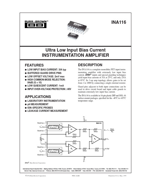
Ultra Low Input Bias Current INSTRUMENTATION AMPLIFIER
FEATURES
q LOW INPUT BIAS CURRENT: 3fA typ q BUFFERED GUARD DRIVE PINS q LOW OFFSET VOLTAGE: 2mV max q HIGH COMMON-MODE REJECTION:
84dB (G = 10) q LOW QUIESCENT CURRENT: 1mA q INPUT OVER-VOLTAGE PROTECTION: ±40V
APPLICATIONS
q LABORATORY INSTRUMENTATION q pH MEASUREMENT q ION–SPECIFIC PROBES q LEAKAGE CURRENT MEASUREMENT
DESCRIPTION
The INA116 is a complete monolithic FET-input instrumentation amplifier with extremely low input bias current. Difet ® inputs and special guarding techniques yield input bias currents of 3fA at 25°C, and only 25fA at 85°C. Its 3-op amp topology allows gains to be set from 1 to 1000 by connecting a single external resistor.
LF13333中文资料
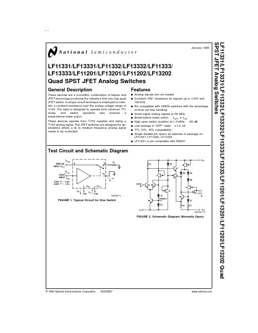
LF11331/LF13331/LF11332/LF13332/LF11333/LF13333/LF11201/LF13201/LF11202/LF13202Quad SPST JFET Analog SwitchesGeneral DescriptionThese devices are a monolithic combination of bipolar and JFET technology producing the industry’s first one chip quad JFET switch.A unique circuit technique is employed to main-tain a constant resistance over the analog voltage range of ±10V.The input is designed to operate from minimum TTL levels,and switch operation also ensures a break-before-make action.These devices operate from ±15V supplies and swing a ±10V analog signal.The JFET switches are designed for ap-plications where a dc to medium frequency analog signal needs to be controlled.Featuresn Analog signals are not loadedn Constant “ON”resistance for signals up to ±10V and 100kHzn Pin compatible with CMOS switches with the advantage of blow out free handlingn Small signal analog signals to 50MHz n Break-before-make action:t OFF <t ONn High open switch isolation at 1.0MHz:−50dB n Low leakage in “OFF”state:<1.0nA n TTL,DTL,RTL compatibilityn Single disable pin opens all switches in package on LF11331,LF11332,LF11333n LF11201is pin compatible with DG201Test Circuit and Schematic DiagramDS005667-2FIGURE 1.Typical Circuit for One SwitchDS005667-12FIGURE 2.Schematic Diagram (Normally Open)January 1995LF11331/LF13331/LF11332/LF13332/LF11333/LF13333/LF11201/LF13201/LF11202/LF13202Quad SPST JFET Analog Switches©1999National Semiconductor Corporation Absolute Maximum Ratings(Note1)If Military/Aerospace specified devices are required, please contact the National Semiconductor Sales Office/ Distributors for availability and specifications.(Note2)Supply Voltage(V CC−V EE)36V Reference Voltage V EE≤V R≤V CC Logic Input Voltage V R−4.0V≤V IN≤V R+6.0V Analog Voltage V EE≤V A≤V CC+6V;V A≤V EE+36V Analog Current|I A|<20mA Power Dissipation(Note3)Molded DIP(N Suffix)500mW Cavity DIP(D Suffix)900mW Operating Temperature RangeLF11201,2and LF11331,2,3−55˚C to+125˚C LF13201,2and LF13331,2,30˚C to+70˚C Storage Temperature−65˚C to+150˚C Soldering InformationN and D Package(10sec.)300˚C SO Package:Vapor Phase(60sec.)215˚C Infrared(15sec.)220˚CElectrical Characteristics(Note4)LF11331/2/3LF13331/2/3Symbol Parameter Conditions LF11201/2LF13201/2UnitsMin Typ Max Min Typ MaxR ON“ON”Resistance V A=0,I D=1mA T A=25˚C150200150250Ω200300200350ΩR ON Match“ON”Resistance Matching T A=25˚C5201050ΩV A Analog Range±10±11±10±11V I S(ON)+Leakage Current in“ON”Condition Switch“ON,”V S=V D=±10V T A=25˚C0.350.310nA I D(ON)3100330nA I S(OFF)Source Current in“OFF”Condition Switch“OFF,”V S=+10V,T A=25˚C0.450.410nAV D=−10V3100330nA I D(OFF)Drain Current in“OFF”Condition Switch“OFF,”V S=+10V,T A=25˚C0.150.110nAV D=−10V3100330nA V INH Logical“1”Input Voltage 2.0 2.0V V INL Logical“0”Input Voltage0.80.8VI INH Logical“1”Input Current V IN=5V T A=25˚C 3.610253.640100µAI INL Logical“0”Input Current V IN=0.8T A=25˚C0.10.1µA11µA t ON Delay Time“ON”V S=±10V,(Figure3)T A=25˚C500500ns t OFF Delay Time“OFF”V S=±10V,(Figure3)T A=25˚C9090ns t ON−t OFF Break-Before-Make V S=±10V,(Figure3)T A=25˚C8080ns C S(OFF)Source Capacitance Switch“OFF,”V S=±10V T A=25˚C 4.0 4.0pF C D(OFF)Drain Capacitance Switch“OFF,”V D=±10V T A=25˚C 3.0 3.0pF C S(ON)+Active Source and Drain Capacitance Switch“ON,”V S=V D=0V T A=25˚C 5.0 5.0pF C D(ON)I SO(OFF)“OFF”Isolation(Figure4),(Note5)T A=25˚C−50−50dB CT Crosstalk(Figure4),(Note5)T A=25˚C−65−65dB SR Analog Slew Rate(Note6)T A=25˚C5050V/µsI DIS Disable Current(Figure5),(Note7)T A=25˚C0.4 1.00.6 1.5mA0.6 1.50.9 2.3mAI EE Negative Supply Current All Switches“OFF,”V S=±10V T A=25˚C 3.0 5.0 4.37.0mA4.27.5 6.010.5mAI R Reference Supply Current All Switches“OFF,”V S=±10V T A=25˚C 2.0 4.0 2.7 5.0mA2.8 6.03.87.5mAI CC Positive Supply Current All Switches“OFF,”V S=±10V T A=25˚C 4.5 6.07.09.0mA6.39.09.813.5mANote1:“Absolute Maximum Ratings”indicate limits beyond which damage to the device may occur.Operating Ratings indicate conditions for which the device is functional,but do not guarantee specific performance limits.Note2:Refer to RETSF11201X,RETSF11331X,RETSF11332X and RETSF11333X for military specifications.Note3:For operating at high temperature the molded DIP products must be derated based on a+100˚C maximum junction temperature and a thermal resistance of+150˚C/W,devices in the cavity DIP are based on a+150˚C maximum junction temperature and are derated at±100˚C/W.2Electrical Characteristics(Note4)(Continued)Note4:Unless otherwise specified,V CC=+15V,V EE=−15V,V R=0V,and limits apply for−55˚C≤T A≤+125˚C for the LF11331/2/3and the LF11201/2,−25˚C≤T A≤+85˚C for the LF13331/2/3and the LF13201/2.Note5:These parameters are limited by the pin to pin capacitance of the package.Note6:This is the analog signal slew rate above which the signal is distorted as a result of finite internal slew rates.Note7:All switches in the device are turned“OFF”by saturating a transistor at the disable node as shown in Figure5.The delay time will be approximately equal to the t ON or t OFF plus the delay introduced by the external transistor.Note8:This graph indicates the analog current at which1%of the analog current is lost when the drain is positive with respect to the source.Note9:θJA(Typical)Thermal ResistanceMolded DIP(N)85˚C/WCavity DIP(D)100˚C/WSmall Outline(M)105˚C/WConnection Diagrams(Top View for SO and Dual-In-Line Packages)(All Switches Shown are For Logical“0”)LF11331/LF13331DS005667-1LF11332/LF13332DS005667-13LF11333/LF13333DS005667-14LF11201/LF13201DS005667-15 3Connection Diagrams(Top View for SO and Dual-In-Line Packages)(All Switches Shown are For Logical “0”)(Continued)LF11202/LF13202DS005667-16Order Number LF13201D,LF11201D,LF11201D/883,LF13202D,LF11202D,LF11202D/883,LF13331D,LF11331D, LF11331D/883,LF13332D,LF11332D,LF11332D/883,LF13333D,LF11333D or LH11333D/883See NS Package Number D16COrder Number LF13201M,LF13202M,LF13331M,LF13332M or LF13333MSee NS Package Number M16AOrder Number LF13201N,LF13202N,LF13331N,LF13332N or LF13333NSee NS Package Number N16A4Test Circuit and Typical Performance CurvesDelay Time,Rise Time,Settling Time,andSwitching TransientsDS005667-17DS005667-18DS005667-19DS005667-20DS005667-21DS005667-225Additional Test CircuitsTypical Performance CharacteristicsDS005667-39DS005667-40FIGURE 3.t ON ,t OFF Test Circuit and Waveforms for a Normally Open SwitchDS005667-41FIGURE 4.“OFF”Isolation,Crosstalk,Small Signal Response“ON”ResistanceDS005667-23“ON”ResistanceDS005667-24“ON”ResistanceDS005667-25 6Typical Performance Characteristics(Continued)Break-Before-Make ActionDS005667-26Switching TimesDS005667-27Crosstalk and“OFF”Isolation vs FrequencyUsing Test Circuit ofFigure5DS005667-28Supply CurrentDS005667-29Supply CurrentDS005667-30Supply CurrentDS005667-31Switch Leakage CurrentsDS005667-32Switch Leakage CurrentDS005667-33Switch CapacitancesDS005667-34 7Typical Performance Characteristics(Continued)Application HintsGENERAL INFORMATIONThese devices are monolithic quad JFET analog switches with “ON”resistances which are essentially independent of analog voltage or analog current.The leakage currents are typically less than 1nA at 25˚C in both the “OFF”and “ON”switch states and introduce negligible errors in most applica-tions.Each switch is controlled by minimum TTL logic levels at its input and is designed to turn “OFF”faster than it will turn “ON.”This prevents two analog sources from being tran-siently connected together during switching.The switches were designed for applications which require break-before-make action,no analog current loss,medium speed switching times and moderate analog currents.Because these analog switches are JFET rather than CMOS,they do not require special handling.LOGIC INPUTSThe logic input (IN),of each switch,is referenced to two for-ward diode drops (1.4V at 25˚C)from the reference supply (V R )which makes it compatible with DTL,RTL,and TTL logic families.For normal operation,the logic “0”voltage can range from 0.8V to −4.0V with respect to V R and the logic “1”voltage can range from 2.0V to 6.0V with respect to V R ,pro-vided V IN is not greater than (V CC −2.5V).If the input voltage is greater than (V CC −2.5V),the input current will increase.Ifthe input voltage exceeds 6.0V or −4.0V with respect to V R ,a resistor in series with the input should be used to limit the input current to less than 100µA.ANALOG VOLTAGE AND CURRENTAnalog VoltageEach switch has a constant “ON”resistance (R ON )for analog voltages from (V EE +5V)to (V CC −5V).For analog voltages greater than (V CC −5V),the switch will remain ON indepen-dent of the logic input voltage.For analog voltages less than (V EE +5V),the ON resistance of the switch will increase.Al-though the switch will not operate normally when the analog voltage is out of the previously mentioned range,the source voltage can go to either (V EE +36V)or (V CC +6V),whichever is more positive,and can go as negative as V EE without de-struction.The drain (D)voltage can also go to either (V EE +36V)or (V CC +6V),whichever is more positive,and can go as negative as (V CC −36V)without destruction.Analog CurrentWith the source (S)positive with respect to the drain (D),the R ON is constant for low analog currents,but will increase at higher currents (>5mA)when the FET enters the saturation region.However,if the drain is positive with respect to the source and a small analog current loss at high analog cur-rents (Note 6)is tolerable,a low R ON can be maintained for analog currents greater than 5mA at 25˚C.Slew Rate of Analog Voltage Above Which Signal Loading OccursDS005667-35Small Signal ResponseDS005667-36Maximum Accurate Analog Current vs TemperatureDS005667-37Logical “1”Input Bias CurrentDS005667-38 8Application Hints(Continued)LEAKAGE CURRENTSThe drain and source leakage currents,in both the ON and the OFF states of each switch,are typically less than1nA at 25˚C and less than100nA at125˚C.As shown in the typical curves,these leakage currents are Dependent on power supply voltages,analog voltage,analog current and the source to drain voltage.DELAY TIMESThe delay time OFF(t OFF)is essentially independent of both the analog voltage and temperature.The delay time ON (t ON)will decrease as either(V CC−V A)decreases or the tem-perature decreases.POWER SUPPLIESThe voltage between the positive supply(V CC)and either the negative supply(V EE)or the reference supply(V R)can be as much as36V.To accommodate variations in input logic refer-ence voltages,V R can range from V EE to(V CC−4.5V).Care should be taken to ensure that the power supply leads for the device never become reversed in polarity or that the device is never inadvertently installed backwards in a test socket.If one of these conditions occurs,the supplies would zener an internal diode to an unlimited current;and result in a de-stroyed device.SWITCHING TRANSIENTSWhen a switch is turned OFF or ON,transients will appear at the load due to the internal transient voltage at the gate of the switch JFET being coupled to the drain and source by the junction capacitances of the JFET.The magnitude of these transients is dependent on the load.A lower value R L produces a lower transient voltage.A negative transient oc-curs during the delay time ON,while a positive transient oc-curs during the delay time OFF.These transients are rela-tively small when compared to faster switch families. DISABLE NODEThis node can be used,as shown in Figure5,to turn all the switches in the unit off independent of logic inputs.Normally, the node floats freely at an internal diode drop(≈0.7V)above V R.When the external transistor in Figure5is saturated,the node is pulled very close to V R and the unit is disabled.Typi-cally,the current from the node will be less than1mA.This feature is not available on the LF11201or LF11202series.Typical ApplicationsDS005667-6FIGURE5.Disable FunctionSample and Hold with ResetDS005667-42 9Typical Applications(Continued)Programmable Inverting Non-Inverting Operational AmplifierDS005667-43Programmable Gain Operational AmplifierDS005667-44 10Typical Applications(Continued)DemultiplexerDS005667-45Multiplexer/MixerDS005667-4611Typical Applications(Continued)8-Channel Analog Commutator with6-Channel Select LogicDS005667-47Chopper Channel AmplifierDS005667-48 12Typical Applications(Continued)Self-Zeroing Operational AmplifierDS005667-49Programmable Integrator with Reset and HoldDS005667-5013Typical Applications(Continued)Staircase Transfer Function Operational AmplifierDS005667-51 14Typical Applications(Continued)DSB Modulator-DemodulatorDS005667-111516Physical Dimensions inches(millimeters)unless otherwise notedOrder Number LF11201D,LF11201D/883,LF13201D,LF11202D,LF11202D/883,LF13202D,LF11331D,LF11331D/883,LF13331D,LF11332D,LF11332D/883,LF13332D,LF11333D,LF11333D/883or LF13333DNS Package Number D16COrder Number LF113201M,LF13202M,LF13331M,LF13332M or LF13333MNS Package Number M16A17Physical Dimensions inches(millimeters)unless otherwise noted(Continued)LIFE SUPPORT POLICYNATIONAL’S PRODUCTS ARE NOT AUTHORIZED FOR USE AS CRITICAL COMPONENTS IN LIFE SUPPORT DE-VICES OR SYSTEMS WITHOUT THE EXPRESS WRITTEN APPROVAL OF THE PRESIDENT OF NATIONAL SEMI-CONDUCTOR CORPORATION.As used herein:1.Life support devices or systems are devices or sys-tems which,(a)are intended for surgical implant intothe body,or(b)support or sustain life,and whose fail-ure to perform when properly used in accordancewith instructions for use provided in the labeling,canbe reasonably expected to result in a significant injuryto the user.2.A critical component is any component of a life supportdevice or system whose failure to perform can be rea-sonably expected to cause the failure of the life supportdevice or system,or to affect its safety or effectiveness.National SemiconductorCorporationAmericasTel:1-800-272-9959Fax:1-800-737-7018Email:support@National SemiconductorEuropeFax:+49(0)180-5308586Email:europe.support@Deutsch Tel:+49(0)180-5308585English Tel:+49(0)180-5327832Français Tel:+49(0)180-5329358Italiano Tel:+49(0)180-5341680National SemiconductorAsia Pacific CustomerResponse GroupTel:65-2544466Fax:65-2504466Email:sea.support@National SemiconductorJapan Ltd.Tel:81-3-5639-7560Fax:81-3-5639-7507Order Number LF13201N,LF13202N,LF13331N,LF13332N or LF13333NNS Package Number N16ALF11331/LF13331/LF11332/LF13332/LF11333/LF13333/LF1121/LF1321/LF1122/LF1322QuadSPSTJFETAnalogSwitchesNational does not assume any responsibility for use of any circuitry described,no circuit patent licenses are implied and National reserves the right at any time without notice to change said circuitry and specifications.。
MSC.333(90)中文版

海安会MSC.333(90)决议(2012年5月22日通过)通过经修订的船载航行数据记录仪(VDR)性能标准海上安全委员会,忆及国际海事组织公约第28(b)条关于本委员会的职能,还忆及大会A.886(21)决议,决定应由海上安全委员会和/或海上环境保护委员会(如适合)代表本组织履行通过性能标准和技术说明及其修正案的职能,进一步忆及本委员会在其81届会议上通过的经MSC.214(81)决议修订的,大会在其20届会议上通过的A.861(20)决议《船载航行数据记录仪(VDR)性能标准》,认识到修订VDR性能标准的必要性以协助调查人员伤亡,审议了航行安全分委会在其57次会议上提出的建议案,1. 通过经修订的船载航行数据记录仪(VDR)性能标准的建议案,其文本载于本决议附件;2. 建议各国政府确保:.1 在2014年7月1日或以后安装的VDR符合不低于本决议附件规定的性能标准;和.2 在2014年7月1日以前安装的VDR符合不低于经MSC.214(81)决议修正的A.861(20)决议附件规定的性能标准。
附件关于船载航行数据记录仪(VDR)性能标准的建议案1目的航行数据记录仪(VDR)是以一种可靠且可读取的结构用于储存船舶在发生有影响的事故前后一段时间有关的船舶位置、动态、实际状况、指挥和控制信息。
主管机关和船东均能获取VDR内的信息。
这些信息用于随后的安全调查以确定事故原因。
2适用范围经修正的SOLAS第V章中规定的某些类型船舶要求配备性能不低于该性能标准规定的VDR。
3参考资料3.1IMO决议:− A.694(17) 关于作为全球海上遇险和安全系统(GMDSS)组成部分的船载无线电设备和电子助航设备的一般要求;− A.810(19) 在406MHz上工作的自浮式卫星应急无线电示位标(EPIRB)的性能标准;和− A.1021(26) 2009年警报器和指示器规则。
3.2IMO通函:−MSC/Circ.982 驾驶台设备和布置的人机工程学衡准指南。
INA333AIDGKR中文资料

Sample Request
Click Here
150kW
150kW
A3 50kW
PACKAGE/ORDERING INFORMATION (1)
PRODUCT INA333 (1) (2) PACKAGE-LEAD MSOP-8 DFN-8 (2) PACKAGE DESIGNATOR DGK DRG PACKAGE MARKING I333 I333A
For the most current package and ordering information see the Package Option Addendum at the end of this document, or see the TI web site at . Available Q4, 2008.
6
VOUT
150kW
150kW
5
REF
INA333 4 VG=1+ 100kW RG
1
2
Please be aware that an important notice concerning availability, standard warranty, and use in critical applications of Texas Instruments semiconductor products and disclaimers thereto appears at the end of this data sheet. All trademarks are the property of their respective owners.
INA111中文资料

INPUT Offset Voltage, RTI Initial TA = +25°C vs Temperature TA = TMIN to TMAX vs Power Supply VS = ±6V to ±18V Impedance, Differential Common-Mode Input Common-Mode Range VDIFF = 0V Common-Mode Rejection VCM = ±10V, ∆RS = 1kΩ G=1 G = 10 G = 100 G = 1000 BIAS CURRENT OFFSET CURRENT NOISE VOLTAGE, RTI f = 100Hz f = 1kHz f = 10kHz fB = 0.1Hz to 10Hz Noise Current f = 10kHz GAIN Gain Equation Range of Gain Gain Error G = 1000, RS = 0Ω
RG V–IN V
T 75 90 100 100 ±20 ±10
±200 ± 500/G ±2 ± 20/G T T T T T T T T T T T T T T T T
±1000 ± 5000/G ±10 ± 100/G T
µV µV/°C µV/V Ω || pF Ω || pF V dB dB dB dB
T T
DESCRIPTION
The INA111 is a high speed, FET-input instrumentation amplifier offering excellent performance. The INA111 uses a current-feedback topology providing extended bandwidth (2MHz at G = 10) and fast settling time (4µs to 0.01% at G = 100). A single external resistor sets any gain from 1 to over 1000. Offset voltage and drift are laser trimmed for excellent DC accuracy. The INA111’s FET inputs reduce input bias current to under 20pA, simplifying input filtering and limiting circuitry. The INA111 is available in 8-pin plastic DIP, and SOL-16 surface-mount packages, specified for the –40°C to +85°C temperature range.
INA168中文资料
2
元器件交易网
PIN CONFIGURATION
TOP VIEW
OUT 1 GND 2
VI+N 3
5 V+ 4 VI–N
SOT
ABSOLUTE MAXIMUM RATINGS(1)
Supply Voltage, V+ INA138 ............................................................................... –0.3V to 60V INA168 ............................................................................... –0.3V to 60V
PARAMETER
CONDITION
INA138
MIN
TYP
MAX
MIN
INPUT Full-Scale Sense Voltage Common-Mode Input Range Common-Mode Rejection
Offset Voltage(1) vs Temperature vs Power Supply
Input common-mode and power supply voltages are independent and can range from 2.7V to 36V for the INA138 and 2.7V to 60V for the INA168. Both models draw only 25µA quiescent current, which also permits connecting the power supply to either side of the current measurement shunt with minimal error.
INA333 微功耗、零漂移、轨到轨输出仪表放大器说明书

V OUTREFR GProduct FolderSample &BuyTechnical Documents Tools &SoftwareSupport &CommunityINA333ZHCSAK0C –JULY 2008–REVISED DECEMBER 2015INA333微功耗(50μA)、零漂移、轨到轨输出仪表放大器1特性•低偏移电压:25µV (最大值),G ≥100•低漂移:0.1μV/°C ,G ≥100•低噪声:50nV/√Hz ,G ≥100•高共模抑制比(CMRR):100dB (最小值),G ≥10•低输入偏置电流:200pA (最大值)•电源范围:1.8V 至5.5V•输入电压:(V–)+0.1V 至(V+)–0.1V •输出电压:(V–)+0.05V 至(V+)–0.05V •低静态电流:50μA•工作温度范围:-40°C 至+125°C •已过滤射频干扰(RFI)的输入•8引脚VSSOP 和8引脚WSON 封装2应用范围•桥式放大器•心电图(ECG)放大器•压力传感器•医疗仪表•便携式仪表•衡器•热电偶放大器•电阻式温度检测器(RTD)传感器放大器•数据采集3说明INA333器件是一款低功耗的精密仪表放大器,具有出色的精度。
该器件采用通用的三运算放大器设计,并且拥有小巧尺寸和低功耗特性,非常适合各类便携式应用。
可通过单个外部电阻在1到1000范围内设置增益。
INA333设计为采用符合行业标准的增益公式:G =1+(100k Ω/R G )。
INA333器件拥有超低的偏移电压(25μV ,G ≥100),出色的偏移电压漂移(0.1μV/°C ,G ≥100),以及较高的共模抑制比(100dB ,G ≥10)。
该器件可由低至1.8V (±0.9V)的电源供电运行,静态电流仅为50μA ,因此非常适合电池供电类系统。
INA333_中文资料

低失调电压:25μV(最大值),G≥100
低漂移:0.1μV/°C,G≥100
低噪声:50nV/√Hz的,G≥100
高CMRR度:100dB(最小值),G≥10
低输入偏置电流:200PA(最大)
热电偶放大器
RTD传感器放大器
数据采集
1、引脚:
2、封装:
3、绝对最大额定参数:
(1)强调上面这些额定值可能会造成永久性的损害。暴露在绝对最大条件下长时间可能降低器件的可靠性。这些压力额定值只,和设备的这些功能操作或超过任何其他条件这些规定是不是暗示。
(2)输入端有病二极管到电源线。输入信号超出电源线路0.3V,应该被限流在10mA以下。
基本参数:
该INA333是一款低功耗,高精度仪器提供出色的精度。多功能的三运放设计,体积小,低功耗使其非常适用于广泛的便携式应用。
单个外部电阻设置从1到1000的增益,INA333是专为使用业界标准的增益公式而设计
G =1+(100kΩ/ RG)。
该INA333提供了非常低失调电压(25μV,G≥100),出色的失调电压漂移(0.1μV/°C,G≥100),和高共模抑制比(100dB,g≥10)。它工作电源低至1.8V(±0.9V),而静态电流仅为50μA,非常适合电池供电的系统。利用自动校准技术,以确保卓越的精度在扩展工业温度范围,INA333还提供了非常低的噪声密度(50nV/√Hz的)的向下延伸到DC。
电源电压范围:1.8V至+5.5 V
输入电压:(V-)+0.1V至(V +)-0.1V
输出范围:(V-)+0.05V到ቤተ መጻሕፍቲ ባይዱV +)-0.05V
ina333正弦信号采集
ina333正弦信号采集摘要:一、引言二、正弦信号采集的原理1.信号放大2.滤波处理3.模拟信号转换为数字信号三、正弦信号采集的应用领域1.通信系统2.自动控制3.仪器测量四、正弦信号采集的发展趋势1.高精度采集2.高速采集3.智能化采集五、结论正文:一、引言正弦信号采集在现代科技领域中具有广泛的应用,对于信号的获取、分析和处理具有重要意义。
ina333 作为一种常用的正弦信号采集器件,具有出色的性能和稳定性,为各种信号采集应用提供了有力支持。
本文将详细介绍ina333 正弦信号采集的相关知识。
二、正弦信号采集的原理正弦信号采集主要涉及信号放大、滤波处理和模拟信号转换为数字信号三个环节。
首先,信号放大是将微弱的输入信号放大到合适的范围,以便进行后续处理。
其次,滤波处理是为了消除噪声和干扰,提高信号质量。
最后,模拟信号转换为数字信号是将连续变化的模拟信号转换为离散的数字信号,以便于数字电路的处理和存储。
三、正弦信号采集的应用领域正弦信号采集广泛应用于通信系统、自动控制和仪器测量等领域。
在通信系统中,正弦信号采集用于实现信号的调制和解调,保证通信质量。
在自动控制领域,正弦信号采集用于实时监测和控制生产过程,提高自动化水平。
在仪器测量领域,正弦信号采集用于精确测量各种物理量,提高测量准确度。
四、正弦信号采集的发展趋势随着科技的不断进步,正弦信号采集技术也在不断发展。
未来正弦信号采集的发展趋势主要表现在以下几个方面:1.高精度采集:随着信号处理技术的提高,对信号采集的精度要求也越来越高。
因此,高精度信号采集将成为未来的发展趋势。
2.高速采集:在某些应用领域,如通信和自动控制,对信号采集的速度有很高的要求。
因此,高速信号采集技术将成为未来的研究热点。
3.智能化采集:随着人工智能技术的发展,未来的信号采集系统将具备更强的智能化水平,能够自动进行信号识别、处理和分析。
五、结论ina333 正弦信号采集器件凭借其出色的性能和稳定性,在信号采集领域得到了广泛的应用。
ina333正弦信号采集

ina333正弦信号采集摘要:1.了解ina333正弦信号采集的基本概念2.ina333正弦信号采集的原理与方法3.ina333正弦信号采集的应用领域4.总结与展望正文:一、了解ina333正弦信号采集的基本概念ina333是一款具有高精度的电流检测传感器,能实现对正弦波信号的采集。
正弦信号采集在工程、科研等领域具有广泛的应用,对于信号处理、分析以及控制等方面具有重要意义。
二、ina333正弦信号采集的原理与方法1.原理:ina333通过电阻分压的方式,将电流信号转换为电压信号。
电压信号经过放大、滤波等处理,最终输出一个与原始电流信号成正比的电压信号。
2.方法:首先,将ina333与待测电流电路串联;然后,通过信号处理电路对电压信号进行处理;最后,使用相关仪器对处理后的电压信号进行分析和检测。
三、ina333正弦信号采集的应用领域1.电力系统:用于监测电流、电压等参数,确保电力系统的稳定运行。
2.自动化控制:对工业生产过程中的电流、速度等信号进行实时监测,实现自动控制。
3.通信领域:在通信系统中,对信号进行采集、处理和分析,以提高信号传输质量和效率。
4.科研实验:在各类科学研究中,对实验数据进行实时采集和分析,为理论研究提供数据支持。
四、总结与展望ina333正弦信号采集在众多领域具有广泛的应用,为科研和工程提供了有效的数据支持。
随着科技的不断发展,对信号采集技术的要求也越来越高。
未来,ina333正弦信号采集技术将在以下方面进行优化和改进:1.提高采集精度,减小误差。
2.简化信号处理电路,降低成本。
3.提高系统的稳定性和可靠性,延长使用寿命。
4.实现远程监控和智能化分析,提高信号管理的效率。
ina333正弦信号采集
ina333正弦信号采集1. 介绍在电子技术领域中,信号采集是非常重要的一项工作。
而正弦信号采集是其中一种常见的任务。
本文将介绍一种常用的芯片型号ina333,以及如何使用它来采集正弦信号。
2. ina333芯片简介ina333是一种高精度、低功耗的运算放大器芯片。
它具有低输入偏置电流、低温漂移和宽输入电压范围的特点,适用于各种精密测量应用。
2.1 特性•输入电压范围:±Vcc•输入偏置电流:25nA•温度漂移:0.3μV/°C•带宽:10MHz•增益带宽积:50kHz•工作电流:50μA2.2 引脚配置ina333芯片具有8个引脚,其功能如下:1.Vcc:正电源输入2.Vin-:负输入端3.Vin+:正输入端4.Vout:输出端5.Ref-:负参考电压输入6.Ref+:正参考电压输入7.NC:未连接8.Vee:负电源输入3. 正弦信号采集电路设计正弦信号采集电路的设计一般包括信号源、运算放大器和数据采集系统三个部分。
下面将详细介绍每个部分的设计要点。
3.1 信号源信号源是正弦信号的产生器,常用的有函数发生器、振荡器等。
在设计中需要注意信号源的频率范围和输出电平。
3.2 运算放大器运算放大器是信号处理的核心部分,它负责放大信号并进行滤波等处理。
在本设计中,我们选用ina333芯片作为运算放大器。
3.3 数据采集系统数据采集系统包括模数转换器(ADC)、微控制器(MCU)等。
它们将模拟信号转换为数字信号,并进行后续处理和存储。
4. 正弦信号采集实验步骤为了验证正弦信号采集电路的设计,我们可以进行一系列实验。
以下是实验步骤:1.搭建电路:按照设计要求,连接信号源、运算放大器和数据采集系统。
2.设置信号源:调整信号源的频率和输出电平,使其符合实验要求。
3.采集数据:通过数据采集系统,采集运算放大器输出的信号,并将其转换为数字信号。
4.数据处理:使用计算机软件对采集到的数据进行处理和分析,如绘制波形图、计算频率和幅值等。
ina333正弦信号采集

ina333正弦信号采集摘要:一、引言1.介绍ina333 传感器2.阐述正弦信号采集的重要性3.简述本文内容二、ina333 传感器的工作原理1.传感器概述2.工作原理详解3.特性与优势三、正弦信号采集方法1.模拟信号采集2.数字信号采集3.信号处理与分析四、信号采集应用案例1.案例一:基于ina333 的正弦信号采集系统2.案例二:ina333 在工业领域的应用3.案例三:ina333 在医疗领域的应用五、正弦信号采集的发展趋势与展望1.新技术的发展2.行业应用的拓展3.未来市场前景正文:一、引言ina333 是一款广泛应用于正弦信号采集的传感器,它具有高精度、高稳定性等优点,为各种领域提供了可靠的信号采集解决方案。
本文将详细介绍ina333 传感器的工作原理、正弦信号采集方法及应用案例,并展望信号采集领域的发展趋势。
二、ina333 传感器的工作原理ina333 传感器是一款能够将正弦波信号转换为可供后续处理的电信号的设备。
它具有高度集成的特点,内部集成了信号放大、滤波、模数转换等功能模块,可以实现对正弦信号的高精度采集。
1.传感器概述:ina333 是一款三通道电流检测传感器,具有12 位分辨率,广泛应用于工业、医疗、通信等领域。
2.工作原理详解:ina333 通过电流检测电阻将输入电流转换为电压信号,经过内部信号放大、滤波等处理后,将模拟信号转换为数字信号,最终输出可供后续处理的电信号。
3.特性与优势:ina333 具有高精度、高稳定性、低漂移等特性,能够在各种恶劣环境下稳定工作,满足不同应用场景的需求。
三、正弦信号采集方法正弦信号采集方法主要包括模拟信号采集和数字信号采集。
1.模拟信号采集:模拟信号采集设备主要包括模拟多路开关、放大器、滤波器等,通过这些设备将输入的正弦信号转换为可供后续处理的电信号。
2.数字信号采集:数字信号采集设备主要包括模数转换器(ADC)、数字多路开关等,通过这些设备将输入的正弦信号转换为数字信号,以便于后续处理和分析。
REF3333AIDCKR资料

REF33xx PRODUCT FAMILY
PRODUCT REF3312 REF3318 REF3320 REF3325 REF3330 REF3333
DESCRIPTION 1.25V 1.8V 2.048V 2.5V 3.0V 3.3V
1
Please be aware that an important notice concerning availability, standard warranty, and use in critical applications of Texas Instruments semiconductor products and disclaimers thereto appears at the end of this data sheet. All trademarks are the property of their respective owners.
2
PRODUCTION DATA information is current as of publication date. Products conform to specifications per the terms of the Texas Instruments standard warranty. Production processing does not necessarily include testing of all parameters.
- 1、下载文档前请自行甄别文档内容的完整性,平台不提供额外的编辑、内容补充、找答案等附加服务。
- 2、"仅部分预览"的文档,不可在线预览部分如存在完整性等问题,可反馈申请退款(可完整预览的文档不适用该条件!)。
- 3、如文档侵犯您的权益,请联系客服反馈,我们会尽快为您处理(人工客服工作时间:9:00-18:30)。
• BRIDGE AMPLIFIERS • ECG AMPLIFIERS • PRESSURE SENSORS • MEDICAL INSTRUMENTATION • PORTABLE INSTRUMENTATION • WEIGH SCALES • THERMOCOUPLE AMPLIFIERS • RTD SENSOR AMPLIFIERS • DATA ACQUISITION
Human body model (HBM)
ESD rating
Charged device model (CDM)
ห้องสมุดไป่ตู้
Machine model (MM)
INA333 +7
(V–) – 0.3 to (V+) + 0.3 Continuous
–40 to +150 –65 to +150
+150 4000 1000 200
Click Here
V+
7
2 VIN-
RFI Filtered Inputs
A1 RFI Filtered Inputs 1
50kW
RG 8
50kW
150kW
150kW
A3
6 VOUT
3 VIN+
RFI Filtered Inputs RFI Filtered Inputs
A2
4 V-
150kW
150kW
UNIT V V
°C °C °C V V V
(1) Stresses above these ratings may cause permanent damage. Exposure to absolute maximum conditions for extended periods may degrade device reliability. These are stress ratings only, and functional operation of the device at these or any other conditions beyond those specified is not implied.
元器件交易网
INA333
...................................................................................................................................................................................................... SBOS445 – JULY 2008
Copyright © 2008, Texas Instruments Incorporated
元器件交INA易33网3
SBOS445 – JULY 2008 ......................................................................................................................................................................................................
(2) Input terminals are diode-clamped to the power-supply rails. Input signals that can swing more than 0.3V beyond the supply rails should be current limited to 10mA or less.
ESD damage can range from subtle performance degradation to complete device failure. Precision integrated circuits may be more susceptible to damage because very small parametric changes could cause the device not to meet its published specifications.
Micro-Power (50µA), Zerø-Drift, Rail-to-Rail Out Instrumentation Amplifier
FEATURES
1
•2 LOW OFFSET VOLTAGE: 25µV (max), G ≥ 100 • LOW DRIFT: 0.1µV/°C, G ≥ 100 • LOW NOISE: 50nV/√Hz, G ≥ 100 • HIGH CMRR: 100dB (min), G ≥ 10 • LOW INPUT BIAS CURRENT: 200pA (max) • SUPPLY RANGE: +1.8V to +5.5V • INPUT VOLTAGE: (V–) +0.1V to (V+) –0.1V • OUTPUT RANGE: (V–) +0.05V to (V+) –0.05V • LOW QUIESCENT CURRENT: 50µA • OPERATING TEMPERATURE: –40°C to +125°C • RFI FILTERED INPUTS • MSOP-8 AND DFN-8 PACKAGES
2
PRODUCTION DATA information is current as of publication date. Products conform to specifications per the terms of the Texas Instruments standard warranty. Production processing does not necessarily include testing of all parameters.
(3) Short-circuit to ground.
DGK PACKAGE MSOP-8
(TOP VIEW)
PIN CONFIGURATIONS
DRG PACKAGE DFN-8
(TOP VIEW)
RG 1 VIN- 2 VIN+ 3
V- 4
INA333
8 RG 7 V+ 6 VOUT 5 REF
RG 1 VIN- 2 VIN+ 3
V- 4
Exposed Thermal Die Pad
on Underside
8 RG 7 V+ 6 VOUT 5 REF
INA333
2
Submit Documentation Feedback
Product Folder Link(s): INA333
Copyright © 2008, Texas Instruments Incorporated
PACKAGE/ORDERING INFORMATION(1)
PRODUCT INA333
PACKAGE-LEAD MSOP-8 DFN-8 (2)
PACKAGE DESIGNATOR DGK DRG
PACKAGE MARKING I333 I333A
(1) For the most current package and ordering information see the Package Option Addendum at the end of this document, or see the TI web site at .
元器件交易网
INA333
...................................................................................................................................................................................................... SBOS445 – JULY 2008
The INA333 is available in both MSOP-8 and DFN-8 surface-mount packages and is specified over the TA = –40°C to +125°C temperature range.
blank
Sample Request
A single external resistor sets any gain from 1 to 1000. The INA333 is designed to use an industry-standard gain equation: G = 1 + (100kΩ/RG).
The INA333 provides very low offset voltage (25µV, G ≥ 100), excellent offset voltage drift (0.1µV/°C, G ≥ 100), and high common-mode rejection (100dB at G ≥ 10). It operates with power supplies as low as 1.8V (±0.9V), and quiescent current is only 50µA—ideal for battery-operated systems. Using autocalibration techniques to ensure excellent precision over the extended industrial temperature range, the INA333 also offers exceptionally low noise density (50nV/√Hz) that extends down to dc.