NVFMCS25DC48V1.5BR中文资料
MAX485中文数据手册资料
MAX485中文资料2009-11-28 14:49MAX485中文资料,MAX485 PDF,DATASHEET,电路图,通讯程序内容介绍:MAX481、MAX483、MAX485、MAX487-MAX491以及MAX1487是用于RS-485与RS-422通信的低功耗收发器,每个器件中都具有一个驱动器和一个接收器。
MAX483、MAX487、MAX488以及MAX489具有限摆率驱动器,可以减小EMI,并降低由不恰当的终端匹配电缆引起的反射,实现最高250kbps 的无差错数据传输。
MAX481、MAX485、MAX490、MAX491、MAX1487的驱动器摆率不受限制,可以实现最高2.5Mbps的传输速率。
这些收发器在驱动器禁用的空载或满载状态下,吸取的电源电流在120(A 至500(A 之间。
另外,MAX481、MAX483与MAX487具有低电流关断模式,仅消耗0.1µA。
所有器件都工作在5V单电源下。
驱动器具有短路电流限制,并可以通过热关断电路将驱动器输出置为高阻状态,防止过度的功率损耗。
接收器输入具有失效保护特性,当输入开路时,可以确保逻辑高电平输出。
MAX481,MAX483,MAX485,MAX487,MAX1487引脚(管脚)图及工作电路MAX485通讯程序与MAX232通讯程序在本质上是一样的,只是MAX485通讯程序需要加上通讯方向控制。
下面是基于mega128 16AU的485通信中断接收的程序,调试通过,晶振为外部16M,MAX485的DE和RE短接连PC0口,程序如下:#define SEND_485 PORTC|=0x01#define READ_485 PORTC&=0xfevoid Usart1_init(void) //16Mhz频率,设置波特率9.6k,8位数据位,无校验,接收发送使能,1位停止位{UBRR1H=0;UBRR1L=103;UCSR1B=(1<<RXCIE1)|(1<<RXEN1)|(1<<TXEN1); //发送接收使能,使用中断方式,UCSR1C=(1<<UCSZ10)|(1<<UCSZ11); //0x06 8位数据,1位停止位,无校验}void Usart1_transmit(unsigned char c) //查询方式发送接收字符函数{SEND_485;DelayBus();DelayBus();DelayBus();while( !(UCSR1A&(1<<UDRE1)));//等待发送缓冲区为空UDR1=c;while(!(UCSR1A&(1<<TXC1)));// UDCR0=c;UCSR1A |= _BV(TXC1);//将发送结束标志位清零// SET_BIT(UCSR1A,);READ_485;direction++;}SIGNAL(SIG_UART1_RECV)//serial port 1 {if(UCSR1A&(1<<RXC1)){rec1buff=UDR1;rec1_flag=1;。
MAX485CPA+中文资料
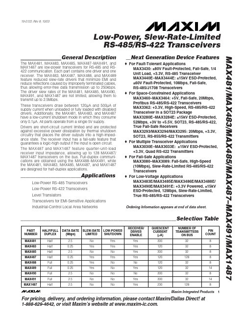
For pricing, delivery, and ordering information,please contact Maxim/Dallas Direct!at 1-888-629-4642, or visit Maxim’s website at .General DescriptionThe MAX481, MAX483, MAX485, MAX487–MAX491, and MAX1487 are low-power transceivers for RS-485 and RS-422 communication. Each part contains one driver and one receiver. The MAX483, MAX487, MAX488, and MAX489feature reduced slew-rate drivers that minimize EMI and reduce reflections caused by improperly terminated cables,thus allowing error-free data transmission up to 250kbps.The driver slew rates of the MAX481, MAX485, MAX490,MAX491, and MAX1487 are not limited, allowing them to transmit up to 2.5Mbps.These transceivers draw between 120µA and 500µA of supply current when unloaded or fully loaded with disabled drivers. Additionally, the MAX481, MAX483, and MAX487have a low-current shutdown mode in which they consume only 0.1µA. All parts operate from a single 5V supply.Drivers are short-circuit current limited and are protected against excessive power dissipation by thermal shutdown circuitry that places the driver outputs into a high-imped-ance state. The receiver input has a fail-safe feature that guarantees a logic-high output if the input is open circuit.The MAX487 and MAX1487 feature quarter-unit-load receiver input impedance, allowing up to 128 MAX487/MAX1487 transceivers on the bus. Full-duplex communi-cations are obtained using the MAX488–MAX491, while the MAX481, MAX483, MAX485, MAX487, and MAX1487are designed for half-duplex applications.________________________ApplicationsLow-Power RS-485 Transceivers Low-Power RS-422 Transceivers Level TranslatorsTransceivers for EMI-Sensitive Applications Industrial-Control Local Area Networks__Next Generation Device Features♦For Fault-Tolerant ApplicationsMAX3430: ±80V Fault-Protected, Fail-Safe, 1/4Unit Load, +3.3V, RS-485 TransceiverMAX3440E–MAX3444E: ±15kV ESD-Protected,±60V Fault-Protected, 10Mbps, Fail-Safe, RS-485/J1708 Transceivers♦For Space-Constrained ApplicationsMAX3460–MAX3464: +5V, Fail-Safe, 20Mbps,Profibus RS-485/RS-422 TransceiversMAX3362: +3.3V, High-Speed, RS-485/RS-422Transceiver in a SOT23 PackageMAX3280E–MAX3284E: ±15kV ESD-Protected,52Mbps, +3V to +5.5V, SOT23, RS-485/RS-422,True Fail-Safe ReceiversMAX3293/MAX3294/MAX3295: 20Mbps, +3.3V,SOT23, RS-855/RS-422 Transmitters ♦For Multiple Transceiver ApplicationsMAX3030E–MAX3033E: ±15kV ESD-Protected,+3.3V, Quad RS-422 Transmitters ♦For Fail-Safe ApplicationsMAX3080–MAX3089: Fail-Safe, High-Speed (10Mbps), Slew-Rate-Limited RS-485/RS-422Transceivers♦For Low-Voltage ApplicationsMAX3483E/MAX3485E/MAX3486E/MAX3488E/MAX3490E/MAX3491E: +3.3V Powered, ±15kV ESD-Protected, 12Mbps, Slew-Rate-Limited,True RS-485/RS-422 TransceiversMAX481/MAX483/MAX485/MAX487–MAX491/MAX1487Low-Power, Slew-Rate-Limited RS-485/RS-422 Transceivers______________________________________________________________Selection Table19-0122; Rev 8; 10/03Ordering Information appears at end of data sheet.M A X 481/M A X 483/M A X 485/M A X 487–M A X 491/M A X 1487Low-Power, Slew-Rate-Limited RS-485/RS-422 Transceivers 2_______________________________________________________________________________________ABSOLUTE MAXIMUM RATINGSSupply Voltage (V CC ).............................................................12V Control Input Voltage (RE , DE)...................-0.5V to (V CC + 0.5V)Driver Input Voltage (DI).............................-0.5V to (V CC + 0.5V)Driver Output Voltage (A, B)...................................-8V to +12.5V Receiver Input Voltage (A, B).................................-8V to +12.5V Receiver Output Voltage (RO).....................-0.5V to (V CC +0.5V)Continuous Power Dissipation (T A = +70°C)8-Pin Plastic DIP (derate 9.09mW/°C above +70°C)....727mW 14-Pin Plastic DIP (derate 10.00mW/°C above +70°C)..800mW 8-Pin SO (derate 5.88mW/°C above +70°C).................471mW14-Pin SO (derate 8.33mW/°C above +70°C)...............667mW 8-Pin µMAX (derate 4.1mW/°C above +70°C)..............830mW 8-Pin CERDIP (derate 8.00mW/°C above +70°C).........640mW 14-Pin CERDIP (derate 9.09mW/°C above +70°C).......727mW Operating Temperature RangesMAX4_ _C_ _/MAX1487C_ A...............................0°C to +70°C MAX4__E_ _/MAX1487E_ A.............................-40°C to +85°C MAX4__MJ_/MAX1487MJA...........................-55°C to +125°C Storage Temperature Range.............................-65°C to +160°C Lead Temperature (soldering, 10sec).............................+300°CDC ELECTRICAL CHARACTERISTICS(V CC = 5V ±5%, T A = T MIN to T MAX , unless otherwise noted.) (Notes 1, 2)Stresses beyond those listed under “Absolute Maximum Ratings” may cause permanent damage to the device. These are stress ratings only, and functional operation of the device at these or any other conditions beyond those indicated in the operational sections of the specifications is not implied. Exposure to absolute maximum rating conditions for extended periods may affect device reliability.V V IN = -7VV IN = 12V V IN = -7V V IN = 12V Input Current (A, B)I IN2V TH k Ω48-7V ≤V CM ≤12V, MAX487/MAX1487R INReceiver Input Resistance -7V ≤V CM ≤12V, all devices except MAX487/MAX1487R = 27Ω(RS-485), Figure 40.4V ≤V O ≤2.4VR = 50Ω(RS-422)I O = 4mA, V ID = -200mV I O = -4mA, V ID = 200mV V CM = 0V-7V ≤V CM ≤12V DE, DI, RE DE, DI, RE MAX487/MAX1487,DE = 0V, V CC = 0V or 5.25VDE, DI, RE R = 27Ωor 50Ω, Figure 4R = 27Ωor 50Ω, Figure 4R = 27Ωor 50Ω, Figure 4DE = 0V;V CC = 0V or 5.25V,all devices except MAX487/MAX1487CONDITIONSk Ω12µA ±1I OZRThree-State (high impedance)Output Current at ReceiverV 0.4V OL Receiver Output Low Voltage 3.5V OH Receiver Output High Voltage mV 70∆V TH Receiver Input Hysteresis V -0.20.2Receiver Differential Threshold Voltage-0.2mA 0.25mA-0.81.01.55V OD2Differential Driver Output (with load)V 2V 5V OD1Differential Driver Output (no load)µA±2I IN1Input CurrentV 0.8V IL Input Low Voltage V 2.0V IH Input High Voltage V 0.2∆V OD Change in Magnitude of Driver Common-Mode Output Voltage for Complementary Output States V 0.2∆V OD Change in Magnitude of Driver Differential Output Voltage for Complementary Output States V 3V OC Driver Common-Mode Output VoltageUNITS MINTYPMAX SYMBOL PARAMETERMAX481/MAX483/MAX485/MAX487–MAX491/MAX1487Low-Power, Slew-Rate-Limited RS-485/RS-422 Transceivers_______________________________________________________________________________________3SWITCHING CHARACTERISTICS—MAX481/MAX485, MAX490/MAX491, MAX1487(V CC = 5V ±5%, T A = T MIN to T MAX , unless otherwise noted.) (Notes 1, 2)DC ELECTRICAL CHARACTERISTICS (continued)(V CC = 5V ±5%, T A = T MIN to T MAX , unless otherwise noted.) (Notes 1, 2)ns 103060t PHLDriver Rise or Fall Time Figures 6 and 8, R DIFF = 54Ω, C L1= C L2= 100pF ns MAX490M, MAX491M MAX490C/E, MAX491C/E2090150MAX481, MAX485, MAX1487MAX490M, MAX491MMAX490C/E, MAX491C/E MAX481, MAX485, MAX1487Figures 6 and 8, R DIFF = 54Ω,C L1= C L2= 100pF MAX481 (Note 5)Figures 5 and 11, C RL = 15pF, S2 closedFigures 5 and 11, C RL = 15pF, S1 closed Figures 5 and 11, C RL = 15pF, S2 closed Figures 5 and 11, C RL = 15pF, S1 closed Figures 6 and 10, R DIFF = 54Ω,C L1= C L2= 100pFFigures 6 and 8,R DIFF = 54Ω,C L1= C L2= 100pF Figures 6 and 10,R DIFF = 54Ω,C L1= C L2= 100pF CONDITIONS ns 510t SKEW ns50200600t SHDNTime to ShutdownMbps 2.5f MAX Maximum Data Rate ns 2050t HZ Receiver Disable Time from High ns 103060t PLH 2050t LZ Receiver Disable Time from Low ns 2050t ZH Driver Input to Output Receiver Enable to Output High ns 2050t ZL Receiver Enable to Output Low 2090200ns ns 134070t HZ t SKD Driver Disable Time from High |t PLH - t PHL |DifferentialReceiver Skewns 4070t LZ Driver Disable Time from Low ns 4070t ZL Driver Enable to Output Low 31540ns51525ns 31540t R , t F 2090200Driver Output Skew to Output t PLH , t PHL Receiver Input to Output4070t ZH Driver Enable to Output High UNITS MIN TYP MAX SYMBOL PARAMETERFigures 7 and 9, C L = 100pF, S2 closed Figures 7 and 9, C L = 100pF, S1 closed Figures 7 and 9, C L = 15pF, S1 closed Figures 7 and 9, C L = 15pF, S2 closedM A X 481/M A X 483/M A X 485/M A X 487–M A X 491/M A X 1487Low-Power, Slew-Rate-Limited RS-485/RS-422 Transceivers 4_______________________________________________________________________________________SWITCHING CHARACTERISTICS—MAX483, MAX487/MAX488/MAX489(V CC = 5V ±5%, T A = T MIN to T MAX , unless otherwise noted.) (Notes 1, 2)SWITCHING CHARACTERISTICS—MAX481/MAX485, MAX490/MAX491, MAX1487 (continued)(V CC = 5V ±5%, T A = T MIN to T MAX , unless otherwise noted.) (Notes 1, 2)3001000Figures 7 and 9, C L = 100pF, S2 closed Figures 7 and 9, C L = 100pF, S1 closed Figures 5 and 11, C L = 15pF, S2 closed,A - B = 2VCONDITIONSns 40100t ZH(SHDN)Driver Enable from Shutdown toOutput High (MAX481)nsFigures 5 and 11, C L = 15pF, S1 closed,B - A = 2Vt ZL(SHDN)Receiver Enable from Shutdownto Output Low (MAX481)ns 40100t ZL(SHDN)Driver Enable from Shutdown toOutput Low (MAX481)ns 3001000t ZH(SHDN)Receiver Enable from Shutdownto Output High (MAX481)UNITS MINTYP MAX SYMBOLPARAMETERt PLH t SKEW Figures 6 and 8, R DIFF = 54Ω,C L1= C L2= 100pFt PHL Figures 6 and 8, R DIFF = 54Ω,C L1= C L2= 100pFDriver Input to Output Driver Output Skew to Output ns 100800ns ns 2000MAX483/MAX487, Figures 7 and 9,C L = 100pF, S2 closedt ZH(SHDN)Driver Enable from Shutdown to Output High2502000ns2500MAX483/MAX487, Figures 5 and 11,C L = 15pF, S1 closedt ZL(SHDN)Receiver Enable from Shutdown to Output Lowns 2500MAX483/MAX487, Figures 5 and 11,C L = 15pF, S2 closedt ZH(SHDN)Receiver Enable from Shutdown to Output Highns 2000MAX483/MAX487, Figures 7 and 9,C L = 100pF, S1 closedt ZL(SHDN)Driver Enable from Shutdown to Output Lowns 50200600MAX483/MAX487 (Note 5) t SHDN Time to Shutdownt PHL t PLH , t PHL < 50% of data period Figures 5 and 11, C RL = 15pF, S2 closed Figures 5 and 11, C RL = 15pF, S1 closed Figures 5 and 11, C RL = 15pF, S2 closed Figures 5 and 11, C RL = 15pF, S1 closed Figures 7 and 9, C L = 15pF, S2 closed Figures 6 and 10, R DIFF = 54Ω,C L1= C L2= 100pFFigures 7 and 9, C L = 15pF, S1 closed Figures 7 and 9, C L = 100pF, S1 closed Figures 7 and 9, C L = 100pF, S2 closed CONDITIONSkbps 250f MAX 2508002000Maximum Data Rate ns 2050t HZ Receiver Disable Time from High ns 25080020002050t LZ Receiver Disable Time from Low ns 2050t ZH Receiver Enable to Output High ns 2050t ZL Receiver Enable to Output Low ns ns 1003003000t HZ t SKD Driver Disable Time from High I t PLH - t PHL I DifferentialReceiver SkewFigures 6 and 10, R DIFF = 54Ω,C L1= C L2= 100pFns 3003000t LZ Driver Disable Time from Low ns 2502000t ZL Driver Enable to Output Low ns Figures 6 and 8, R DIFF = 54Ω,C L1= C L2= 100pFns 2502000t R , t F 2502000Driver Rise or Fall Time ns t PLH Receiver Input to Output2502000t ZH Driver Enable to Output High UNITS MIN TYP MAX SYMBOL PARAMETERMAX481/MAX483/MAX485/MAX487–MAX491/MAX1487Low-Power, Slew-Rate-Limited RS-485/RS-422 Transceivers_______________________________________________________________________________________530002.5OUTPUT CURRENT vs.RECEIVER OUTPUT LOW VOLTAGE525M A X 481-01OUTPUT LOW VOLTAGE (V)O U T P U T C U R R E N T (m A )1.515100.51.02.0203540450.90.1-50-252575RECEIVER OUTPUT LOW VOLTAGE vs.TEMPERATURE0.30.7TEMPERATURE (°C)O U T P U TL O W V O L T A G E (V )500.50.80.20.60.40100125-20-41.5 2.0 3.0 5.0OUTPUT CURRENT vs.RECEIVER OUTPUT HIGH VOLTAGE-8-16M A X 481-02OUTPUT HIGH VOLTAGE (V)O U T P U T C U R R E N T (m A )2.5 4.0-12-18-6-14-10-203.54.5 4.83.2-50-252575RECEIVER OUTPUT HIGH VOLTAGE vs.TEMPERATURE3.64.4TEMPERATURE (°C)O U T P UT H I G H V O L T A G E (V )0504.04.63.44.23.83.01001259000 1.0 3.0 4.5DRIVER OUTPUT CURRENT vs.DIFFERENTIAL OUTPUT VOLTAGE1070M A X 481-05DIFFERENTIAL OUTPUT VOLTAGE (V)O U T P U T C U R R E N T (m A )2.0 4.05030806040200.5 1.5 2.53.5 2.31.5-50-2525125DRIVER DIFFERENTIAL OUTPUT VOLTAGEvs. TEMPERATURE1.72.1TEMPERATURE (°C)D I F FE R E N T I A L O U T P U T V O L T A G E (V )751.92.21.62.01.8100502.4__________________________________________Typical Operating Characteristics(V CC = 5V, T A = +25°C, unless otherwise noted.)NOTES FOR ELECTRICAL/SWITCHING CHARACTERISTICSNote 1:All currents into device pins are positive; all currents out of device pins are negative. All voltages are referenced to deviceground unless otherwise specified.Note 2:All typical specifications are given for V CC = 5V and T A = +25°C.Note 3:Supply current specification is valid for loaded transmitters when DE = 0V.Note 4:Applies to peak current. See Typical Operating Characteristics.Note 5:The MAX481/MAX483/MAX487 are put into shutdown by bringing RE high and DE low. If the inputs are in this state for lessthan 50ns, the parts are guaranteed not to enter shutdown. If the inputs are in this state for at least 600ns, the parts are guaranteed to have entered shutdown. See Low-Power Shutdown Mode section.M A X 481/M A X 483/M A X 485/M A X 487–M A X 491/M A X 1487Low-Power, Slew-Rate-Limited RS-485/RS-422 Transceivers 6___________________________________________________________________________________________________________________Typical Operating Characteristics (continued)(V CC = 5V, T A = +25°C, unless otherwise noted.)120008OUTPUT CURRENT vs.DRIVER OUTPUT LOW VOLTAGE20100M A X 481-07OUTPUT LOW VOLTAGE (V)O U T P U T C U R R E N T (m A )6604024801012140-1200-7-5-15OUTPUT CURRENT vs.DRIVER OUTPUT HIGH VOLTAGE-20-80M A X 481-08OUTPUT HIGH VOLTAGE (V)O U T P U T C U R R E N T (m A )-31-603-6-4-2024-100-40100-40-60-2040100120MAX1487SUPPLY CURRENT vs. TEMPERATURE300TEMPERATURE (°C)S U P P L Y C U R R E N T (µA )20608050020060040000140100-50-2550100MAX481/MAX485/MAX490/MAX491SUPPLY CURRENT vs. TEMPERATURE300TEMPERATURE (°C)S U P P L Y C U R R E N T (µA )257550020060040000125100-50-2550100MAX483/MAX487–MAX489SUPPLY CURRENT vs. TEMPERATURE300TEMPERATURE (°C)S U P P L Y C U R R E N T (µA )257550020060040000125MAX481/MAX483/MAX485/MAX487–MAX491/MAX1487Low-Power, Slew-Rate-Limited RS-485/RS-422 Transceivers_______________________________________________________________________________________7______________________________________________________________Pin DescriptionFigure 1. MAX481/MAX483/MAX485/MAX487/MAX1487 Pin Configuration and Typical Operating CircuitM A X 481/M A X 483/M A X 485/M A X 487–M A X 491/M A X 1487__________Applications InformationThe MAX481/MAX483/MAX485/MAX487–MAX491 and MAX1487 are low-power transceivers for RS-485 and RS-422 communications. The MAX481, MAX485, MAX490,MAX491, and MAX1487 can transmit and receive at data rates up to 2.5Mbps, while the MAX483, MAX487,MAX488, and MAX489 are specified for data rates up to 250kbps. The MAX488–MAX491 are full-duplex trans-ceivers while the MAX481, MAX483, MAX485, MAX487,and MAX1487 are half-duplex. In addition, Driver Enable (DE) and Receiver Enable (RE) pins are included on the MAX481, MAX483, MAX485, MAX487, MAX489,MAX491, and MAX1487. When disabled, the driver and receiver outputs are high impedance.MAX487/MAX1487:128 Transceivers on the BusThe 48k Ω, 1/4-unit-load receiver input impedance of the MAX487 and MAX1487 allows up to 128 transceivers on a bus, compared to the 1-unit load (12k Ωinput impedance) of standard RS-485 drivers (32 trans-ceivers maximum). Any combination of MAX487/MAX1487 and other RS-485 transceivers with a total of 32 unit loads or less can be put on the bus. The MAX481/MAX483/MAX485 and MAX488–MAX491 have standard 12k ΩReceiver Input impedance.Low-Power, Slew-Rate-Limited RS-485/RS-422 Transceivers 8_______________________________________________________________________________________Figure 2. MAX488/MAX490 Pin Configuration and Typical Operating CircuitFigure 3. MAX489/MAX491 Pin Configuration and Typical Operating CircuitMAX483/MAX487/MAX488/MAX489:Reduced EMI and ReflectionsThe MAX483 and MAX487–MAX489 are slew-rate limit-ed, minimizing EMI and reducing reflections caused by improperly terminated cables. Figure 12 shows the dri-ver output waveform and its Fourier analysis of a 150kHz signal transmitted by a MAX481, MAX485,MAX490, MAX491, or MAX1487. High-frequency har-monics with large amplitudes are evident. Figure 13shows the same information displayed for a MAX483,MAX487, MAX488, or MAX489 transmitting under the same conditions. Figure 13’s high-frequency harmonics have much lower amplitudes, and the potential for EMI is significantly reduced.MAX481/MAX483/MAX485/MAX487–MAX491/MAX1487Low-Power, Slew-Rate-Limited RS-485/RS-422 Transceivers_______________________________________________________________________________________9_________________________________________________________________Test CircuitsFigure 4. Driver DC Test Load Figure 5. Receiver Timing Test LoadFigure 6. Driver/Receiver Timing Test Circuit Figure 7. Driver Timing Test LoadM A X 481/M A X 483/M A X 485/M A X 487–M A X 491/M A X 1487Low-Power, Slew-Rate-Limited RS-485/RS-422 Transceivers 10_______________________________________________________Switching Waveforms_________________Function Tables (MAX481/MAX483/MAX485/MAX487/MAX1487)Figure 8. Driver Propagation DelaysFigure 9. Driver Enable and Disable Times (except MAX488 and MAX490)Figure 10. Receiver Propagation DelaysFigure 11. Receiver Enable and Disable Times (except MAX488and MAX490)Table 1. TransmittingTable 2. ReceivingLow-Power Shutdown Mode (MAX481/MAX483/MAX487)A low-power shutdown mode is initiated by bringing both RE high and DE low. The devices will not shut down unless both the driver and receiver are disabled.In shutdown, the devices typically draw only 0.1µA of supply current.RE and DE may be driven simultaneously; the parts are guaranteed not to enter shutdown if RE is high and DE is low for less than 50ns. If the inputs are in this state for at least 600ns, the parts are guaranteed to enter shutdown.For the MAX481, MAX483, and MAX487, the t ZH and t ZL enable times assume the part was not in the low-power shutdown state (the MAX485/MAX488–MAX491and MAX1487 can not be shut down). The t ZH(SHDN)and t ZL(SHDN)enable times assume the parts were shut down (see Electrical Characteristics ).It takes the drivers and receivers longer to become enabled from the low-power shutdown state (t ZH(SHDN ), t ZL(SHDN)) than from the operating mode (t ZH , t ZL ). (The parts are in operating mode if the –R —E –,DE inputs equal a logical 0,1 or 1,1 or 0, 0.)Driver Output ProtectionExcessive output current and power dissipation caused by faults or by bus contention are prevented by two mechanisms. A foldback current limit on the output stage provides immediate protection against short cir-cuits over the whole common-mode voltage range (see Typical Operating Characteristics ). In addition, a ther-mal shutdown circuit forces the driver outputs into a high-impedance state if the die temperature rises excessively.Propagation DelayMany digital encoding schemes depend on the differ-ence between the driver and receiver propagation delay times. Typical propagation delays are shown in Figures 15–18 using Figure 14’s test circuit.The difference in receiver delay times, | t PLH - t PHL |, is typically under 13ns for the MAX481, MAX485,MAX490, MAX491, and MAX1487 and is typically less than 100ns for the MAX483 and MAX487–MAX489.The driver skew times are typically 5ns (10ns max) for the MAX481, MAX485, MAX490, MAX491, and MAX1487, and are typically 100ns (800ns max) for the MAX483 and MAX487–MAX489.MAX481/MAX483/MAX485/MAX487–MAX491/MAX1487Low-Power, Slew-Rate-Limited RS-485/RS-422 Transceivers______________________________________________________________________________________1110dB/div0Hz5MHz500kHz/div10dB/div0Hz5MHz500kHz/divFigure 12. Driver Output Waveform and FFT Plot of MAX481/MAX485/MAX490/MAX491/MAX1487 Transmitting a 150kHz SignalFigure 13. Driver Output Waveform and FFT Plot of MAX483/MAX487–MAX489 Transmitting a 150kHz SignalM A X 481/M A X 483/M A X 485/M A X 487–M A X 491/M A X 1487Low-Power, Slew-Rate-Limited RS-485/RS-422 Transceivers 12______________________________________________________________________________________V CC = 5V T A = +25°CV CC = 5V T A = +25°CV CC = 5V T A = +25°CV CC = 5V T A = +25°CFigure 14. Receiver Propagation Delay Test CircuitFigure 15. MAX481/MAX485/MAX490/MAX491/MAX1487Receiver t PHLFigure 16. MAX481/MAX485/MAX490/MAX491/MAX1487Receiver t PLHPHL Figure 18. MAX483, MAX487–MAX489 Receiver t PLHLine Length vs. Data RateThe RS-485/RS-422 standard covers line lengths up to 4000 feet. For line lengths greater than 4000 feet, see Figure 23.Figures 19 and 20 show the system differential voltage for the parts driving 4000 feet of 26AWG twisted-pair wire at 110kHz into 120Ωloads.Typical ApplicationsThe MAX481, MAX483, MAX485, MAX487–MAX491, and MAX1487 transceivers are designed for bidirectional data communications on multipoint bus transmission lines.Figures 21 and 22 show typical network applications circuits. These parts can also be used as line repeaters, with cable lengths longer than 4000 feet, as shown in Figure 23.To minimize reflections, the line should be terminated at both ends in its characteristic impedance, and stub lengths off the main line should be kept as short as possi-ble. The slew-rate-limited MAX483 and MAX487–MAX489are more tolerant of imperfect termination.MAX481/MAX483/MAX485/MAX487–MAX491/MAX1487Low-Power, Slew-Rate-Limited RS-485/RS-422 Transceivers______________________________________________________________________________________13DIV Y -V ZRO5V 0V1V0V -1V5V 0V2µs/divFigure 19. MAX481/MAX485/MAX490/MAX491/MAX1487 System Differential Voltage at 110kHz Driving 4000ft of Cable Figure 20. MAX483, MAX487–MAX489 System Differential Voltage at 110kHz Driving 4000ft of CableFigure 21. MAX481/MAX483/MAX485/MAX487/MAX1487 Typical Half-Duplex RS-485 NetworkM A X 481/M A X 483/M A X 485/M A X 487–M A X 491/M A X 1487Low-Power, Slew-Rate-Limited RS-485/RS-422 Transceivers 14______________________________________________________________________________________Figure 22. MAX488–MAX491 Full-Duplex RS-485 NetworkFigure 23. Line Repeater for MAX488–MAX491Isolated RS-485For isolated RS-485 applications, see the MAX253 and MAX1480 data sheets.MAX481/MAX483/MAX485/MAX487–MAX491/MAX1487Low-Power, Slew-Rate-Limited RS-485/RS-422 Transceivers______________________________________________________________________________________15_______________Ordering Information_________________Chip TopographiesMAX481/MAX483/MAX485/MAX487/MAX1487N.C. RO 0.054"(1.372mm)0.080"(2.032mm)DE DIGND B N.C.V CCARE * Contact factory for dice specifications.__Ordering Information (continued)M A X 481/M A X 483/M A X 485/M A X 487–M A X 491/M A X 1487Low-Power, Slew-Rate-Limited RS-485/RS-422 Transceivers 16______________________________________________________________________________________TRANSISTOR COUNT: 248SUBSTRATE CONNECTED TO GNDMAX488/MAX490B RO 0.054"(1.372mm)0.080"(2.032mm)N.C. DIGND Z A V CCYN.C._____________________________________________Chip Topographies (continued)MAX489/MAX491B RO 0.054"(1.372mm)0.080"(2.032mm)DE DIGND Z A V CCYREMAX481/MAX483/MAX485/MAX487–MAX491/MAX1487Low-Power, Slew-Rate-Limited RS-485/RS-422 Transceivers______________________________________________________________________________________17Package Information(The package drawing(s) in this data sheet may not reflect the most current specifications. For the latest package outline information go to /packages .)S O I C N .E P SM A X 481/M A X 483/M A X 485/M A X 487–M A X 491/M A X 1487Low-Power, Slew-Rate-Limited RS-485/RS-422 Transceivers 18______________________________________________________________________________________Package Information (continued)(The package drawing(s) in this data sheet may not reflect the most current specifications. For the latest package outline information go to /packages .)MAX481/MAX483/MAX485/MAX487–MAX491Low-Power, Slew-Rate-Limited RS-485/RS-422 TransceiversMaxim cannot assume responsibility for use of any circuitry other than circuitry entirely embodied in a Maxim product. No circuit patent licenses are implied. Maxim reserves the right to change the circuitry and specifications without notice at any time.Maxim Integrated Products, 120 San Gabriel Drive, Sunnyvale, CA 94086 408-737-7600 ____________________19©2003 Maxim Integrated ProductsPrinted USAis a registered trademark of Maxim Integrated Products.M A X 481/M A X 483/M A X 485/M A X 487–M A X 491/M A X 1487P D I P N .E PSPackage Information (continued)(The package drawing(s) in this data sheet may not reflect the most current specifications. For the latest package outline information go to /packages .)。
英赛威产品手册版

KZ释放电压
VDC
KZ电流
mA
GND
正常工作功耗
W
工作电压范围VDC
最低电压
最高电压
12V
5V-12V
2V-0V
>5mA
与电源共地
<2W
9V
15V
注意:1.供电电源要求:DC +12V0.5A电源纹波:≤50mV继电器电源端并联电解电容≥1000UF。
2.本继电器在带载中不允许直接断开电源,否则会造成继电器的损坏!
4.1 P3V30系列(300V,10-30A,12V线圈电压,一组常开,PCB规格)9
4.2 P3V20系列(300V,10-20A,12V线圈电压,双刀单掷,PCB规格)10
五、400VDC继电器………………………………………………………………..11
5.1N4V40系列(400V,10-40A,12V线圈电压,一组常开)………..….11.
第二个字母代表同等电压,电流的第几套模具,A代表第一套,B代表第二套等。
后面两个数字表示该系列最大电流,如70表示最大电流70A。
最后一个字母代表触点型式及线圈电压,A代表12V线圈电压及一组常开型,B代表12V线圈电压及二组常开型。
三、200VDC继电器
P2V80系列性能介绍
P2A40A/P2A60A/P2A80A
二、产品命名规则
我司继电器产品比较多,因此我司产品按不同电压分为各种系列,每个系列下再包含几个产品,因此命名规则分为系列命名和产品命名两种。
系列命名规则如下(以P6V70为例):
P6V70
第一个字母代表继电器的规格,P表示线路板引出端规格,N表示常规规格。
第一个数字和第二个字母代表直流电压,如6V表示600VDC。
VR25中文资料

High Ohmic/High Voltage Resistors For technical questions contact: ff3dresistors@Document Number: 28732168Revision: 06-Dec-05VR25Vishay BCcomponentsFEATURES•High pulse loading capability •Small size•Lead (Pb)-free solder contacts•Pure tin plating provides compatibility with lead (Pb)-free and lead containing soldering processes•Compatible with "Restriction of the use of Hazardous Substances" (RoHS) directive 2002/95/EC (issue 2004)APPLICATIONS•Where high resistance, high stability and high reliability at high voltage are required •High humidity environment •White goods •Power suppliesA metal glazed film is deposited on a high grade ceramic body.After a helical groove has been cut in the resistive layer, tinned electrolytic copper wires are welded to the end-caps. The resistors are coated with a light blue lacquer which provideselectrical, mechanical, and climatic protection.The encapsulation is resistant to all cleaning solvents in accordance with “MIL-STD 202E, method 215” and “IEC 60068-2-45”.Note1.Ohmic values (other than resistance range) are available on request.TECHNICAL SPECIFICATIONSDESCRIPTION VALUE Resistance range 1)100k Ωto 22M ΩResistance tolerance and series:100k Ω to 15M Ω ± 1 %: E24/E96 series; ± 5 %: E24series 15M Ω to 22M Ω± 5 %: E24series; ± 10 %: E12seriesMaximum dissipation at T amb =70°C 0.25 W Thermal resistance, R th 140K/W Temperature coefficient≤ ± 200×10-6/KMaximum permissible voltage:DC 1600V RMS1150V Dielectric withstanding voltage of the insulation for 1 minute 700 V Basic specificationsIEC 60115-1B Climatic category (IEC 60068)55/155/56Stability after:load (1000hours)∆R/R max.:± 1.5 %+0.1Ωaccelerated damp heat test (6days)∆R/R max.:± 1.5 %+0.1Ωlong term damp heat test (56days)∆R/R max.:± 1.5 %+0.1ΩNoisemax.5µV/V12NC INFORMATION•The resistors have a 12-digit numeric code starting with 2322241•The subsequent:first digit for 1 % tolerance products (E24 and E96 series) or 2digits for 5 %(E24series)and 10 % (E12series)indicate the resistor type and packing.•The remaining digits indicate the resistance value:–The first 3digits for 1 % or 2digits for 5and 10 %tolerance products indicate the resistance value.–The last digit indicates the resistance decade.Last Digit of 12NC Indicating Resistance Decade12NC ExampleThe 12NC for a VR25, resistor value 7.5M Ω,5 % tolerance,supplied on a bandolier of 1000 units in ammopack, is:232224113755.RESISTANCE DECADELAST DIGIT100to 976k Ω41to 9.76M Ω5≥ 10M Ω6Document Number: 28732For technical questions contact: ff3dresistors@Revision: 06-Dec-05169VR25High Ohmic/High Voltage ResistorsVishay BCcomponents12NC - resistor type and packingTYPETOL.(%)ORDERING CODE 2322241.....BANDOLIER IN AMMOPACKBANDOLIER ON REELRADIAL TAPEDSTRAIGHT LEADS 4000 units52 mm 26 mm 52 mm 52 mm 1000 units 2000 units 5000 units 5000 units VR25± 10....8....-7.... 6....± 536...13...43...53...23...± 10-12...42...52...22...NoteProducts can be ordererd using either the 12NC or the PART NUMBER. The PART NUMBER is shown to facilitate the introduction of a unified part numbering system. Currently, this PART NUMBER is applicable in the Americas only.PART NUMBERPART NUMBER: VR25000001503JA100MODEL/SIZE SPECIAL CHARACTER TC/MATERIAL VALUE TOLERANCE PACKING 1)SPECIAL VR250000 = neutral Z = value overflow(Special)0 = standard3 digit value 1 digit multiplier Multiplier:3 = *1034 = *1045 = *105F = ± 1 %J = ± 5 %K = ± 10 %A5A2A1R5N4The 2 digits are used for all special parts.00 = standardPRODUCT DESCRIPTION: VR25 5 % A1 150KVR25 5 %A1150KMODEL/SIZETOLERANCEPACKING 1)RESISTANCE VALUEVR25± 1 %± 5 %± 10 %A1A547K = 47 K Ω50R1 = 50.1 Ω1) Please refer to table PACKING.PACKINGCODE PIECES DESCRIPTIONMODEL/SIZEA55000Bandolier in ammopack straight leads 52 mm VR25A22000Bandolier in ammopack straight leads 26 mm A11000Bandolier in ammopack straight leads 52 mm R55000Bandolier on reel straight leads 52 mm N44000Bandolier in ammopack radial taped502R V00001503J A 100 For technical questions contact: ff3dresistors@Document Number: 28732170Revision: 06-Dec-05VR25Vishay BCcomponentsHigh Ohmic/High Voltage ResistorsDIMENSIONSMARKINGThe nominal resistance and tolerance are marked on the resistor using four or five colored bands in accordance with IEC publication 60062 “Color codes for fixed resistors”.Yellow and grey are used instead of gold and silver because metal particles in the lacquer could affect high-voltage properties.OUTLINESThe length of the body (L 1) is measured by inserting the leads into holes of two identical gauge plates and moving these plates parallel to each other until the resistor body is clamped without deformation (“IEC publication 60294”).OutlineDIMENSIONS - resistor type and relevant physical dimensionsTYPE ∅ D MAX.L 1MAX.L 2MAX.∅ d VR252.56.57.50.58± 0.05MASS PER 100 UNITSTYPE MASS (g)VR25 52 mm 21.2VR25 26 mm14.8FUNCTIONAL PERFORMANCE PRODUCT CHARACTERIZATIONStandard values of nominal resistance are taken from the E96/E24/E12 series for resistors with a tolerance of ± 1 %, 5 % or 10 %. The values of the E96/E24/E12 series are in accordance with “IEC publication 60063”.Note1.The maximum voltage that may be continuously applied to the resistor element, see “IEC publication 60115-1”.The maximum permissible hot-spot temperature is 155°C.LIMITING VALUESTYPELIMITING VOLTAGE 1)(V)LIMITING POWER(W)DCRMS VR25160011500.25Document Number: 28732For technical questions contact: ff3dresistors@Revision: 06-Dec-05171VR25High Ohmic/High Voltage ResistorsVishay BCcomponentsDeratingPulse Loading CapabilityMaximum dissipation (P max ) in percentage of rated poweras a function of the ambient temperature (T amb )The power that the resistor can dissipate depends on the operating temperature.Maximum allowed peak pulse voltage in accordance with “IEC 60065 chapter 14.1”; 50discharges from a 1nF capacitor charged to ; 12discharges/minute (drift ∆R/R≤2 %)V max Application InformationHot-spot temperature rise (∆T) as a function of dissipated powerTemperature rise (∆T) at the lead end (soldering point) as a functionof dissipated power at various lead lengths after mounting For technical questions contact: ff3dresistors@Document Number: 28732172Revision: 06-Dec-05VR25Vishay BCcomponentsHigh Ohmic/High Voltage ResistorsTESTS AND REQUIREMENTSEssentially all tests are carried out in accordance with the schedule of “IEC publication 60115-1”, category LCT/UCT/56 (rated temperature range: Lower Category Temperature, Upper Category Temperature; damp heat,long term, 56days). The testing also covers the requirements specified by EIA and EIAJ.The tests are carried out in accordance with IEC publication 60068-2, “Recommended basic climatic and mechanical robustness testing procedure for electronic components” and under standard atmospheric conditions according to “IEC 60068-1”, subclause 5.3.In the Test Procedures and Requirements table the tests and requirements are listed with reference to the relevant clauses of “IEC publications 60115-1and 60068-2”; a short description of the test procedure is also given. In some instances deviations from the IEC recommendations were necessary for our method of specifying.All soldering tests are performed with mildly activated flux.TEST PROCEDURES AND REQUIREMENTSIEC 60115-1 CLAUSE IEC 60068-2 TEST METHOD TESTPROCEDUREREQUIREMENTS4.1621 (U)robustness of terminations:4.16.221 (Ua1)tensile all samples ∅ 0.6mm; load 10N;10s number of failures < 10×10-64.16.321 (Ub)bending half number of samples ∅ 0.6mm; load 5N;4×90°number of failures < 10×10-64.16.421 (Uc)torsion other half of samples 3×360° in opposite directionsno damage∆R/R max.:± 0.5 %+0.05Ω4.1720 (T a)solderability 2s; 235°Cgood tinning; no damage 4.1820 (Tb)resistance to soldering heatthermal shock: 3s; 350°C;3mm from body ∆R/R max.:± 0.5 %+0.05Ω4.1914 (Na)rapid change of temperature 30minutes at - 55°C and 30minutes at + 155°C; 5cycles ∆R/R max.:± 0.5 %+0.05Ω4.2029 (Eb)bump 3×1500 bumps in 3directions; 40g no damage∆R/R max.:± 0.5 %+0.05Ω4.226 (Fc)vibrationfrequency 10to 500Hz; displacement 1.5mm or acceleration 10g; 3directions;total 6hours (3×2hours)no damage∆R/R max.:± 0.5 %+0.05ΩDocument Number: 28732For technical questions contact: ff3dresistors@Revision: 06-Dec-05173VR25High Ohmic/High Voltage ResistorsVishay BCcomponents4.23climatic sequence:4.23.2 2 (Ba)dry heat16hours;155°C4.23.330 (Db)damp heat (accelerated) 1st cycle 24hours;55°C; 90to 100 %RH4.23.4 1 (Aa)cold2hours;- 55°C 4.23.513 (M)low air pressure2hours; 8.5kPa; 15to 35°C 4.23.630 (Db)damp heat (accelerated) remaining cycles 5days; 55°C; 95to 100 %RH R ins min.:103M Ω∆R/R max.:± 1.5 %+0.1Ω4.24.23 (Ca)damp heat (steady state)56days; 40°C; 90to 95 %RH;dissipation 0.01P n ; limiting voltage 100V (DC)∆R/R max.:± 1.5 %+0.1Ω4.25.1endurance1000hours at 70°C; P n or V max ∆R/R max.:± 1.5 %+0.1Ω4.8.4temperature coefficient between - 55°C and + 155°C(TC ×10-6/K)≤ ± 2004.7voltage proof on insulation 700V (RMS) during 1minute; V-blockmethodno breakdown 4.12noise“IEC publication 60195”max.5 µV/V 4.6.1.1insulation resistance 500V (DC) during 1minute; V-blockmethod R ins min.:104M Ω4.13short time overloadroom temperature;dissipation 6.25×P n (voltage not more than 2×limiting voltage); 10cycles;5s on and 45s off ∆R/R max.:± 2.0 %+0.05Ω4.26active flammability “Cheese-cloth test”steps of: 5/10/16/25/40 ×P n (RMS)duration 5minutesno flaming of gauze cylinderOTHER TEST IN ACCORDANCE WITH IEC 606952.2passive flammability “Needle-flame test”application of test flame for 20sno ignition of product;no ignition of under-layer;burning time less than 30sTEST PROCEDURES AND REQUIREMENTSIEC 60115-1 CLAUSE IEC 60068-2 TEST METHODTESTPROCEDUREREQUIREMENTSLegal Disclaimer NoticeVishay Document Number: Revision: 08-Apr-051NoticeSpecifications of the products displayed herein are subject to change without notice. Vishay Intertechnology, Inc., or anyone on its behalf, assumes no responsibility or liability for any errors or inaccuracies.Information contained herein is intended to provide a product description only. No license, express or implied, by estoppel or otherwise, to any intellectual property rights is granted by this document. Except as provided in Vishay's terms and conditions of sale for such products, Vishay assumes no liability whatsoever, and disclaims any express or implied warranty, relating to sale and/or use of Vishay products including liability or warranties relating to fitness for a particular purpose, merchantability, or infringement of any patent, copyright, or other intellectual property right. The products shown herein are not designed for use in medical, life-saving, or life-sustaining applications. Customers using or selling these products for use in such applications do so at their own risk and agree to fully indemnify Vishay for any damages resulting from such improper use or sale.。
NVFMCZ25DC48V1.2AD中文资料
Contact Data
Contact Arrangement Contact Material Contact Rating (resistive) Max. Switching Power Max. Switching Voltage Contact Resistance or Voltage drop Operation Electrical life Mechanical 1A SPSTNO f1C SPDT(B-M) Ag SnO2 , AgNi Ag CdO 1A 25A/14VDC 1C 20A/14VDC 350W 75VDC Max. Switching Current:25A 50m Item 3.12 of IEC255-7 105 Item 3.30 of IEC255-7 107 Item 3.31 of IEC255-7
Ordering Information
NVFM C
Z 20
DC12V 1.5 b
7
D
8 5 Coil rated Voltage(V):DC:6,12,24,48 6 Coil power consumption:1.2:1.2W;1.5:1.5W 7 Terminals b: PCB type;a: plug in type 8 Coil transient suppression: D: with diode; R: with resistant;. NIL: standard
0.031 0.055 0.083 0.094 0.098 0.106 0.126 0.177 0.189 0.127 0.248 0.252 0.315 0.354 0.374 0.453 0.551 0.591 0.610 0.905 1.024
西门子 NXGPro+ 控制系统手册_操作手册说明书
3.4
单元通讯的协议 ............................................................................................................ 36
3.5
NXGpro+ 高级安全 .......................................................................................................37
3.2
功率拓扑 ......................................................................................................................34
3.3
控制系统概述 ...............................................................................................................35
NXGPro+ 控制系统手册
NXGPro+ 控制系统手册
操作手册
AC
A5E50491925J
安全性信息
1
安全注意事项
2
控制系统简介
3
NXGPro+ 控制系统简介
4
硬件用户界面说明
5
参数配置/地址
6
运行控制系统
7
高级的操作功能
8
软件用户界面
9
运行软件
10
故障和报警检修
11
48v开关电源用途
48V开关电源是一种输出电压为48伏特的电源设备,通常用于各种电子设备、通信设备、工业设备和其他应用中。
它的主要用途包括以下几个方面:
通信设备:48V开关电源常用于通信基站、网络设备(如路由器、交换机)、服务器等,为这些设备提供稳定的电源供应。
工业设备:在工业自动化领域,许多设备需要可靠的电源供应,如PLC(可编程逻辑控制器)、工控机、传感器等。
电力设备:一些电力设备,如电力放大器、电源模块,可能需要48V的电源供应。
汽车电子:某些汽车电子系统,如车载娱乐系统、导航系统等,也可能使用48V开关电源。
太阳能和风能系统:在可再生能源系统中,48V电源用于将太阳能板或风力涡轮机产生的电能进行整流和转换,以便为住宅、办公室等提供电力。
医疗设备:在医疗领域,一些医疗设备需要稳定和可靠的电源供应,48V开关电源可用于满足这些需求。
电信设备:48V电源在电信领域中也很常见,用于电话交换机、传输设备等。
数据中心:在大型数据中心中,48V电源可以用于服务器、存储设备等,以提供高效的电力管理。
总之,48V开关电源在各种领域中都有广泛的应用,用于为各种电子和电气设备提供稳定、高效的电源供应。
NT71CS15DC48V0.36中文资料
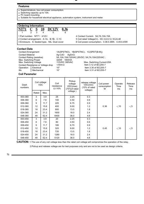
71
Ambient Temperature Relative Humidity 元器件交易网 Mass
2).Inch equivalents are given for general information only.
Reference Data
元器ቤተ መጻሕፍቲ ባይዱ交易网
Features
Superminiature, low coil power consumption. Switching capacity up to 15A. PC board mounting. Suitable for household electrical appliance, automation system, instrument and meter.
Coil Parameter
Coil voltage VDC Pickup voltage VDC(max) (75%of rated voltage ) 2.25 4.50 6.75 9.00 13.5 18.0 36.0 2.25 4.50 6.75 9.00 13.5 18.0 36.0 release voltage VDC(min) (10% of rated voltage) 0.3 0.6 0.9 1.2 1.8 2.4 4.8 0.3 0.6 0.9 1.2 1.8 2.4 4.8
Dash numbers
Coil resistance ±10%
Coil power consumption W
48V电源监控说明书
前面板仅有三个操作按键“UP、Down、OK”,进行各级菜单、功能转换、参数设定等。
a.UP——上翻键:菜单上翻转,改变参数设定、数值增加等操作;
b.OK——平移键(返回键):向同级、同层次菜单进行转移,返回操作;
c.Down——下翻键:菜单下翻转,改变参数设定、数值减少等操作;
4. LCD说明
2.我公司有权利在不通知客户的情况下更改规格书的内容。
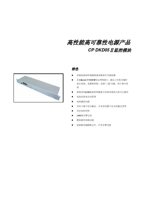
1.模块应用说明
1.1系统框图
CP DKD05Ⅱ监控模块的整个系统工作流图,描述了监控模块、整流模块、整个系统的人机接口,及PC软件远程对系统的操作和配置。组网方式分为RS485组网和TCP/IP组网,都为一点对多点通信(即一台监控PC监控多个系统电源)。
BATL+
3脚
GND
3脚
BATL_NO1
4脚
AC_IC
4脚
ANIN2+
5脚
AC_IB
5脚
ANIN1+
6脚
AC_IA
3P
1脚
COM-4
2P
1脚
GND1
2脚
NC-4
2脚
VCC1
3脚
NO-4
8P
1脚
B4+
3P
1脚
COM-3
2脚
B4-
2脚
NC-3
3脚
B3+
3脚
NO-3
4脚
B3-
3P
1脚
COM-2
5脚
B2+
2脚
故障类型告警名称默认告警级别故障类型告警名称默认告警级别直流配电故障告警系统负载电流过高非紧急告警交流配电故障告警相交流空开紧急告警路低压断开操作非紧急告警相电流过高紧急告警路低压断开操作非紧急告警相电压过高紧急告警环境温度过高非紧急告警相电压过低紧急告警环境温度过低非紧急告警相电压缺相紧急告警电池电流过高非紧急告警相交流空开紧急告警电池温度过高非紧急告警相电流过高紧急告警电池温度过低非紧急告警相电压过高紧急告警传感器1相电压过低紧急告警传感器2相电压缺相紧急告警传感器3相交流空开紧急告警传感器4相电流过高紧急告警直流输出过压紧急告警相电压过高紧急告警电池低压紧急告警相电压过低紧急告警负载熔丝断紧急告警相电压缺相紧急告警电池熔丝断紧急告警整流模块告模块保护告警紧急告警防雷告警紧急告警模块故障告警紧急告警水侵告警紧急告警风机故障告警紧急告警烟雾告警紧急告警限流告警紧急告警规格书高功率密度电源产品版本号
RECOM R5M 5W 隔离 DC DC 电源说明书

DC/DC ConverterDescriptionThe R5M is an isolated 5W DC/DC converter in a compact SMD package available with 4:1 inputs covering 12, 24 and 48V rails providing single or dual regulated, short-circuit protected outputs. There is no minimum load requirement. Isolation is 1.6kVDC/1min, and the operating temperature is from -40°C up to +50°C without derating. Class A and Class B EMC conformity requires only a few external components. Standard packaging is tube.FeaturesRegulated Converters•5W power in SMD package •4:1 Input voltage range •Efficiency up to 86%• 1.6kVDC/1min isolation •Regulated output•-40°C to +50°C at full load•Continuous short circuit protectedR5MSelection GuideModel NumberingY E A Rwa r r a n ty3RoHS 2+compliant 10 from 10Specifications (measured @ Ta= 25°C, nom. Vin, full load and after warm-up unless otherwise stated)Part Input nom. Output Output Efficiency max. CapacitiveNumber Voltage Range (1) Voltage Current typ. (2)Load(3)[VDC] [VDC] [mA] [%] [µF]R5M-xx3.3S/SMD 9-36, 18-75 3.3 1000 774400 R5Mxx05S/SMD 9-36, 18-75 5 1000 812200R5Mxx09S/SMD 9-36, 18-759 55582 1470R5M-xx12S/SMD 9-36, 18-7512 42084-851220 R5M-xx15S/SMD 9-36, 18-7515 333 85-861000R5M-xx24S/SMD 9-36, 18-7524 21082470R5M-xx05D/SMD 9-36, 18-75±5 ±500 82±1000 R5M-xx12D/SMD 9-36, 18-75±12 ±210 84±680 R5M-xx15D/SMD9-36, 18-75±15±168 85±440Notes:Note1: Refer to “Input Voltage Range”Note2: Efficiency is tested at nominal input and full load at +25°C ambient Note3: Max Cap Load is tested at nominal input and full resistive loadBASIC CHARACTERISTICSParameterConditionMin.Typ.Max.Input Voltage Range nom. V IN = 24VDC 9VDC 24VDC 36VDC nom. V IN = 48VDC18VDC48VDC75VDC Input Surge Voltage1 second max.nom. V IN = 24VDC 50VDC nom. V IN = 48VDC 100VDCcontinued on next pageCase Style S ingle/D ualnom. Input Voltage nom. Output VoltageR5M-/SMD5 WattSMDSingle & Dual Outputp re li mi n a rySpecifications (measured @ Ta= 25°C, nom. Vin, full load and after warm-up unless otherwise stated)Specifications (measured @ Ta= 25°C, nom. Vin, full load and after warm-up unless otherwise stated)REGULATIONSParameterConditionValueOutput Accuracy ±1.0% max.Line Regulationlow line to high line, full load±0.2% max.Load Regulation0% to 100% loadsingle 1% max.dual 1% max.10% to 90% loadsingle 0.5% max.dual0.8% max.Cross Regulation asymmetrical 25% / 100% load±5% max.Transient Response Recovery Time25% load step change±500µs typ.PROTECTIONSParameterTypeValueShort Circuit Protection (SCP)continuous, auto recoveryIsolation Voltage (5)I/P to O/P1 minute1.6kVDC min.Isolation Resistance I/P to O/P , V ISO = 500VDC 1G Ω min.Isolation CapacitanceI/P to O/P , 100kHz/0.1V50pF typ.Notes:Note5: This power module is not internally fused. An input line fuse must always be used Recom suggests: 24Vin=T1.25A; 48Vin=T0.63A slow blowp re li mSpecifications (measured @ Ta= 25°C, nom. Vin, full load and after warm-up unless otherwise stated)ENVIRONMENTALParameterConditionValueOperating Temperature Range with derating -40°C to +105°C without derating -40°C to +50°CMaximum Case Temperature measured at “tc point”+105°COperating Humidity non-condensing5% - 95% RH max.Thermal Shock according to MIL-STD-810FVibration according to MIL-STD-810FMTBFaccording to MIL-HDBK-217F, G.B.+25°C2959 x 10³ hoursDerating Graph(@ Chamber and natural convection 0.1m/s)-40-20020407060-30-101030508090120110100100806040907050302010O u t p u t L o a d [%]Ambient Temperature [°C]105i mi n a rySpecifications (measured @ Ta= 25°C, nom. Vin, full load and after warm-up unless otherwise stated)PACKAGING INFORMATIONParameterTypeValuePackaging Dimension (LxWxH)tube 218.0 x 17.2 x 19.9mmPackaging Quantity20pcsStorage Temperature Range non-condensing-55°C to +125°C Storage Humidity5% to 95% RH max.The product information and specifications may be subject to changes even without prior written notice.The product has been designed for various applications; its suitability lies in the responsibility of each customer. The products are not authorized for use in safety-critical applications without RECOM’s explicit written consent. A safety-critical application is an application where a failure may reasonably be expected to endanger or cause loss of life, inflict bodily harm or damage property. The applicant shall indemnify and hold harmless RECOM, its affiliated companies and its representatives against any damage claims in connection with the unauthorizeduse of RECOM products in such safety-critical applications.p r。
尼博星 NV25Axx三相四线系列 25W AC DC模块电源说明书
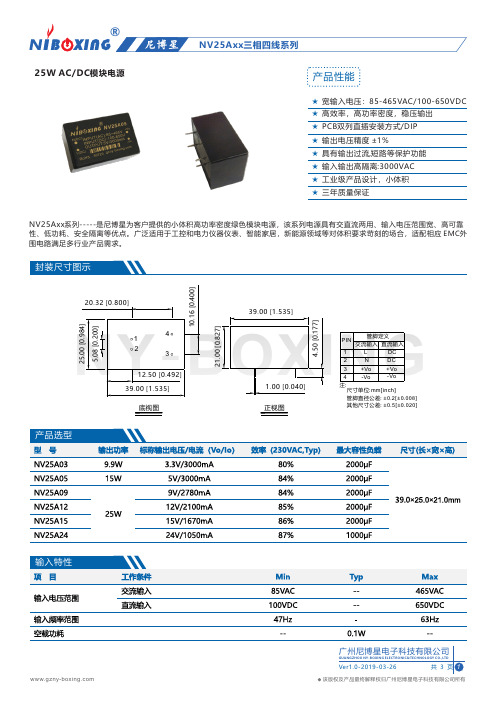
NY -BOXING其他尺寸公差: ±0.5[±0.020]尺寸单位: mm[inch]注:管脚直径公差: ±0.2[±0.008]PIN 管脚定义1234L N +Vo -Vo 交流输入直流输入DC DC -Vo+Vo 12.50 [0.492]20.32 [0.800]25.00[0.984]39.00 [1.535]5.08[0.200]10.16[0.400]底视图123421.00[0.827]1.00 [0.040]4.50[0.177]正视图39.00 [1.535]25W AC/DC 模块电源产品性能★ 宽输入电压:85-465VAC /100-650VDC ★ 高效率,高功率密度,稳压输出★ PCB 双列直插安装方式/DIP ★ 输出电压精度 ±1%★ 具有输出过流,短路等保护功能★ 输入输出高隔离:3000VAC ★ 工业级产品设计,小体积★ 三年质量保证NV25Axx 系列-----是尼博星为客户提供的小体积高功率密度绿色模块电源,该系列电源具有交直流两用、输入电压范围宽、高可靠性、低功耗、安全隔离等优点。
广泛适用于工控和电力仪器仪表、智能家居,新能源领域等对体积要求苛刻的场合,适配相应 EMC 外围电路满足多行业产品需求。
绝缘耐压输入-输出,测试时间60s--3000VAC--工作温度-40℃--+70℃存储温度-40℃+105℃存储湿度----95%RH 开关频率--65KHz --MTBF MIL-HDBK-217F,25°C215,000h 模块外壳材质金属铝外壳输入电流230VAC --250mA --380VAC--150mA--输出功率百分比输入电压降额曲线输入电压(85VAC , 75%)(115VAC , 100%)(430VAC , 100%)(465VAC , 80%)2040608010085160235310385460100(VAC)(100VDC , 75%)210320430540650(VDC)(150VDC , 100%)(600VDC , 100%)(650VDC , 80%)(%)输出功率百分比环境温度温度降额曲线85~465VAC输入电压:100~650VDC020*********-40-200204060(℃)(%)(-40℃, 60%)(-20℃, 100%)(55℃, 100%)(70℃, 60%)1 典型应用电路图示RLAC [L 图[1]典型应用电路2 EMC 解决方案—推荐电路注释1.为应对一般使用要求,建议用户按照典型应用电路搭建电源外围电路2.为获得更优产品输出性能,输出必须接C1,L2,C2,C33.为应对用户对EMC 有高要求,建议用户按照EMC 解决方案推荐电路搭建电源外围电路4.C1,C3:输出滤波电解电容,建议使用低阻电解电容,容量和流过的电流高频 考各厂商提供的技术规格.电容耐.请参 额大于80%.压降5.C3:为陶瓷电容,起去除高频噪声作用注 温馨提示:优先阅读右侧注释注 温馨提示:优先阅读右侧注释RL图[2]EMC 高要求应用电路输出电压C1C25V 2200μF/10V9V 12V 1000μF/25V 2μH(线径大于1MM)15V 24V 680μF/35V L1:差模电感330Hμ元件位号与推荐器件CX :X2电容NF :共模电感FUSE :保险管R1:热敏电阻MOV :压敏电阻功 能抑制差模干扰模块异常时熔断,切断故障抑制浪涌电流吸收雷击浪涌0.33μF/550VAC 10mH-30mH 参考值3.15A /250VAC ,慢熔断(必接)5D-9821KD10抑制共模干扰CY1,CY2:Y 电容1000pF/250V3 输入部分—参数推荐4 输出部分—参数推荐3.3V1000μF/10V680μF/25V 470μF/35VC3L21μF/50V !1.任何一款电源产品不得超过额定输出功率,且不得超出额定输入电压范围;2.若电源产品为多路输出,输出各路必须按比率同时加载;3.无短路保护功能的电源产品严禁出现输出端短路情况;4.若电源产品实物管脚定义与产品选型手册不一致,应以实物管脚定义为准;5.切勿随意改造我司电源产品,由此所造成的一切后果我司概不负责;6.更多产品信息详情请登录我司官方网站()。
艾默生48V电源

DC48V输入,输出30-35V,恒流900MA-电源承认书
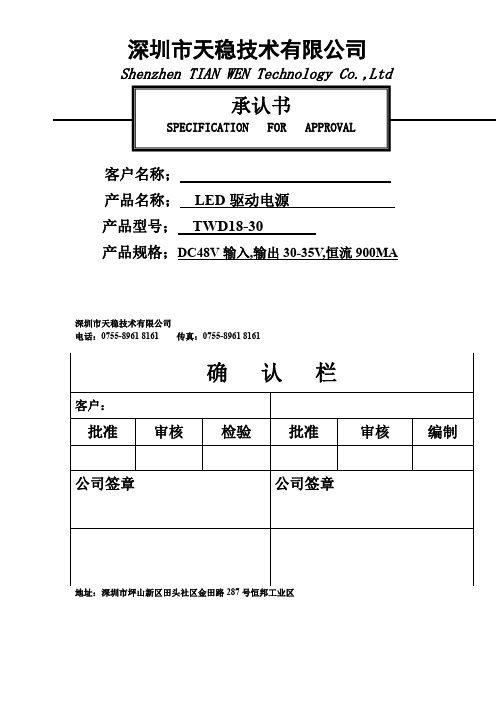
承认书SPECIFICATION FOR APPROVAL客户名称;产品名称;LED驱动电源产品型号;TWD18-30产品规格;DC48V输入,输出30-35V,恒流900MA深圳市天稳技术有限公司电话:0755-8961 8161 传真:0755-8961 8161确认栏客户:批准审核检验批准审核编制公司签章公司签章地址:深圳市坪山新区田头社区金田路287号恒邦工业区产品的概要说明:本电源是一款专为LED设计的高品质,高稳定性的LED防水恒流驱动电源。
具有启动快速,兼容负载范围宽,保护功能齐全,采用国际知名大厂成熟方案,DC48V输入,30-35VDC 输出,高精确的恒流控制,极高的效率和可靠的性能,带主动式PFC,以及小型的外观结构会使你的灯具更加趋于完美。
LED负载概要说明:LED规格为VF=DC30-35V,I=0.9A;最大输出30W。
产品电性参数参数最小典型最大单位输入电流---- 0.7 ---- A输入电压---- 48 ---- VDC 空载功率---- ---0.1- W输出电流0.88 0.9 0.92 A输出电压28 30 35 V输出功率28 30 32 W总效率92 93 95 %使用寿命30000 40000 50000 Hour输入防接反烧坏有电源保护输出短路保护---- 有---- ----OTP过温保护有工作环境温度-20 ---- 70 ℃储存温度-20 ---- 85 ℃工作湿度10 ---- 90 %(Rh)大气压70 ---- 106 Kpa尺寸LED防水电源银白色铝外壳:L53*W42*H31mm 加孔位L70*W42*H31mm输出保护功能:1.输出电压过压保护2.输出最大电压在空载时为48V。
3.输出电流过流保护该驱动为主动限流架构,元件器不损坏情况下电流不会超过最大输出电流。
4.输出自适应功能当LED需求电压降低火串联LED数量减少,LED驱动电源将自动调整输出电压与之相配,使LED正常工作。
YHWKGS100W 四分之一DC DC 说明书

YHWK GS100W 四分之一DC/DC 说明书产品特点◆超宽输入电压范围(4:1)◆效率高达 94%◆隔离电压 2250VDC◆输入欠压保护,输出短路、过流、过压、过温保护◆工作温度范围:-40℃to+85℃◆金属五面屏蔽封装◆1/ 4 砖国际标准引脚方式100W ,宽电压输入,隔离稳压单路 DC/ DC 模块电源传导骚扰抗扰度IEC/EN61000-4-6, EN50121-3-2 10 Vr.m.sperf. Criteria A产品特性曲线YHWK GS100-48S24温度降额曲线(Vin=24V)YHWK GS 100-48S24Z 温度降额曲线(Vin=24V)环境温度(℃)环境温度(℃)YHWK GS100-48S24S 温度降额曲线(Vin=24V)注意事项:1)产品应用热设计需参考推荐的PCB 布局及推荐的散热结构环境温度(℃)注意事项:1)当不使用远端补偿时,确保+Vo 与 sense +,-Vo 与 sense -短接;2)+Vo 与 sense +,-Vo 与 sense -之间的连线尽可能短,并靠近端子。
避免形成一个较大的回路面积,当噪声进入这个回路后,可能造成模块的不稳 定。
2.当使用远端补偿时:尽可能使用双绞线注意事项:1.如果使用远端补偿的引线比较长时,可能导致输出电压不稳定,如果必须使用较长的远端补偿引线时请联系我司技术人员。
2.如果使用远端补偿,请使用双绞线或者屏蔽线,并使引线尽可能短。
3.在电源模块和负载之间请使用宽 PCB 引线或粗线,并保持线路电压降应低于 0.3V 。
确保电源模块的输出电压保持在指定的范围内。
4.引线的阻抗可能造成输出电压振荡或者较大纹波,使用之前请做好足够的评估。
Loa d+Vosense +Trim sense --Vo+CLoa d+Vo sense+ Trim sense--Vo+ C连接线尽可能短Sense 的使用以及注意事项亿鸿维克(1)产品测试及应用时,请按照(图 1)推荐的测试电路进行;至少保障外接一个电解电容 Cin (≥ 220µF ),用于抑制输入端可能产生的浪涌电压。
NOTIFIER NFV-25 50ZS 消防声音撤离控制面板说明书
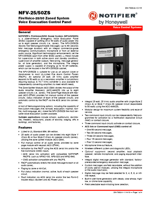
NFV-25/50ZSFireVoice-25/50 Zoned System Voice Evacuation Control PanelDN-7003:A • C-157003p h o 1.j p gGeneralNOTIFIER’s FireVoice-25/50 Zoned System (NFV-25/50ZS)is a state-of-the-art Emergency Voice Evacuation Panel (EVAC) capable of splitting 25 or 50 watts of audio power into up to eight speaker circuits (i.e., zones). The NFV-25/50ZS records five field-programmable messages (up to 60 seconds total message duration) with an integral commercial-grade emergency communications microphone or from an external audio source. Significant technological enhancements set the NFV-25/50ZS apart from other EVAC panels — these include full supervision in both active alarm and standby conditions,supervision of amplifier outputs, field wiring, message genera-tor, all tone generators, and the microphone. The integral power supply is capable of charging up to 18 AH batteries,which can be housed in the NFV-25/50ZS cabinet.The NFV-25/50ZS is suitable for use as an adjunct (slave or stand-alone) to most UL-Listed Fire Alarm Control Panels (FACPs). An optional 25 watt, 25 Vrms audio amplifier expands to 50 watts or as a secondary amplifier in jurisdictions requiring backup. A 70.7 Vrms converter is also available for independently converting amplifiers to meet retrofit needs.The Zone Splitter Module (ACC-ZSM) divides the output of the Audio Amplifier Module(s) (ACC-AAM25) into up to eight speaker circuits (i.e., zones). The Zone Page Module with Key-pad (ACC-ZPMK) provides full manual control of the speaker circuits, status indication of each of the speaker circuits, and automatic control by the FACP via the ACS serial link connec-tion.A host of field-programming options, including the capability of five custom messages (fire, tornado, evacuation, hazmat, non-fire, multi-language, etc.) make the NFV-25/50ZS the most ver-satile voice evacuation system available.Suitable applications include schools, auditoriums, dormito-ries, theaters, restaurants, places of worship, lodging, offic e buildings, and factories.Features•Listed to UL Standard 864, 9th edition.•25 watts of audio power can be divided into eight Style Y (Class B) or four Style Z (Class A) speaker circuits (zones),utilizing the zone splitter module (ACC-ZSM).•Full manual control of all audio zones provided by zone page module with keypad (ACC-ZPMK).•Activation by the FACP using the ACS serial link and/or the five Command (CMD) inputs.–ACS serial link activation with compatible NOTIFIER FACPS: such as NFW2-100, NFS-320 and NFS2-640.–CMD activation compatible with any FACPS.•FACP automatically directs the voice message to each or all audio zones.•Paging by zone or All-Call.•Full status indication (normal, active, fault) of each speaker circuit.•Fault indication via ACS serial link and/or the two Form-C trouble relays (System and AC Power Loss).•Integral 25 watt, 25 Vrms audio amplifier with single Style Z (Class A) or Style Y (Class B) speaker circuit (expandable to 50 watts using the ACC-AAM25).•Modular design for maximum system flexibility and ease of service.•Two command input circuits can be independently field-pro-grammed for activation by a Notification Appliance Circuit (NAC) or contact closure.•Three command input circuits activate on contact closure.•ACS link or Command Input (CMD) control of:–One 60-second message.–Two 30-second messages.–Three 20-second messages.–Four 15-second messages.–Five 12-second messages.•Microphone time-out feature.•Nineteen different system and diagnostic LEDs.•Optional equipment: second amplifier; local playback speaker; remote microphone; and paging equipment inter-face.•Integral digital message generator with standard, factory-prerecorded emergency evacuation message.•Custom messages are field recordable, without the addition of costly add-on modules, utilizing the integral microphone or the audio input jacks.•Digital message may be field-selected for 3, 4, 6, 8, or infi-nite repeat.•Built-in alert tone generators with steady, slow whoop, high/low, or chime tone capability.•Field-selectable lead-in/trailing tone selection.•Alert tone selection may be field-programmed to conform with ANSI S3.41 Audible Emergency Evacuation Signal (Temporal Pattern), per NFP A.•Speaker zone control via ACS serial link, CMD inputs, or keypad•Dual-optically-isolated, trigger input circuits are indepen-dently field-programmable for activation by polarity reversal (host FACP NAC) or dry-contact closure.•Integral diagnostic LEDs include: Power, System Trouble, Microphone Trouble, Message Generator T rouble, Tone Generator T rouble, Amplifier Fault, and others.•ACS serial link or independent Form-C trouble relay allows FACP to monitor voice system while in active (alarm) state.•Integral piezo provides local audible indication for troubles.•Fully supervised in Standby and Active states, including integral microphone, amplifier output, message generator, speaker wiring, and tone generators.•Independent amplifier supervision: current limit, audio level, short circuit protection.•All outputs are power-limited.•Auxiliary power output provides local power for addressable control modules when used to activate the NFV-25/50ZS.•Compatible with all NOTIFIER FACPs, as well as other manufacturers’ panels.Optional ModulesACC-AAM25•25 watt, 25 Vrms audio amplifier module.•Field-programmable for system expansion to 50 watts or asa backup to the primary 25 watt amplifier where required.•Single Class A or Class B speaker circuit.•Plug-in-style terminal blocks for ease of service and mainte-nance.•Fully supervised and power-limited.•Diagnostic LEDs include: yellow “trouble” LED (cable fault, amp fault) and green “amp functional” LED.ACC-EPM•Provides interface to non-fire paging equipment for non-emergency paging applications.•Provides plug-in-style terminal blocks for ease of service and maintenance.•T ransformer-isolated, 600-ohm audio connection to paging equipment.•Electrically-isolated, contact-closure trigger input for activa-tion by the paging equipment.FC-XRM70•Converts 25 Vrms audio outputs to 70.7 Vrms for retrofit applications.•Plugs directly on ACC-AAM25 module(s), allowing indepen-dent conversion to 70.7 Vrms.FC-LPS•Provides local digital message playback for user review of field-recorded custom messages.Controls and IndicatorsLED INDICATORS1.Power On (green).2.System T rouble (yellow).3.Message Generator T rouble (yellow).4.Tone Generator T rouble (yellow).5.Microphone Trouble (yellow).6.Record/Playback (green).7.All-Call (green = Active).8.Audio ON/OFF (green = Active, yellow = Manual Deacti-vation).9.Status of each speaker zone (green = Active, yellow =Manual Deactivation or Fault).Other system LEDs: Battery T rouble, Charger Trouble, Ground Fault, (ACC-AAM25) Speaker Circuit T rouble, and Amplifier Supervisory.Product Line InformationNFV-25/50ZS: 25 watt, 25 Vrms, emergency Voice Evacuation Control Panel (VECP) with integral commercial microphone, digital message generator, zone splitter module (ACC-ZSM), zone page module with keypad (ACC-ZPMK).ACC-AAM25: Optional 25 watt, 25 Vrms Audio Amplifier Mod-ule with single Class A or Class B speaker circuit.ACC-EPM: Optional External Page Module.FC-XRM70: Optional 70.7 Vrms Converter Module (one required per amplifier, consult factory for availability).VEC-RM: Optional Remote Microphone, includes backbox (only one VEC-RM per system).FC-LPS: Optional Local Playback Speaker.BAT Series: Two batteries required. See FACP manual for specific current requirements; see data sheet DN-6933 for overview of batteries.FC-RM: Optional Remote Microphone, includes backbox (only one FC-RM per system.ACC-TR: Optional T rim Ring for semi-flush mounting.SpecificationsPRIMARY POWER (AC)•120 VAC, 60 Hz, 1.5 A.•Wire size: minimum #14 AWG with 600 V insulation.Nonpower-limited, supervised.Secondary Power (Battery) Charging Circuit•Lead-acid batteries only.•Maximum Charging Circuit: Normal Float Charge - 27.6V @0.800 A.•Maximum Charger Capacity: 18 Amp Hour battery. (NFV-25/50ZS Series cabinet holds max. 18 Amp Hour Battery.)AC Loss Relay (TB7)•Operation: normally energized fail-safe relay transfers on AC power loss for independent monitoring by DACT.•AC Loss Relay can be programmed to be the only indication of an AC loss condition (see T able 2-3 on page 31)•AC Loss relay contact rating: 2.0 amps @ 30 VDC (resis-tive), 0.6 amps @ 30 VAC (resistive)Command input circuits (CMD1 and CMD2): •T rigger input voltage: 10.5 – 29 VDC.NOTE: When programmed for reverse-polarity activation.Trouble contact rating:• 2.0 A at 30 VDC (resistive), 0.6 A @ 125 VAC (resistive).Auxiliary power output:•Specific application power: 24 V , 35 mA.Cabinet SpecificationsDoor: 26.174" (66.482 cm) high x 15.780" (40.081 cm) wide x 1.125" (2.858 cm) deep. Backbox: 26.0" (66.040 cm) high x15.5" (39.370 cm) wide x 4.75" (12.065 cm) deep, depth includes door.Temperature and Humidity RangesThis system meets NFPA requirements for operation at 0 –49°C/32 – 120°F and at a relative humidity 93% ± 2% RH (noncondensing) at 32°C ± 2°C (90°F ± 3°F). However, the useful life of the system's standby batteries and the electronic components may be adversely affected by extreme tempera-ture ranges and humidity. Therefore, it is recommended that this system and its peripherals be installed in an environment with a normal room temperature of 15 – 27°C/60 – 80°F .Standards and CodesThe NFV-25/50ZS complies with the following standards:NFP A 72 National Fire Alarm Code; NFP A 101 Life Safety Code; UL 864 Standard for Control Units for Fire Alarm Sys-tems (9th edition).Agency Listings and ApprovalsThe listings and approvals below apply to the basic NFV-25/50ZS control panel. In some cases, certain modules may not be listed by certain approval agencies, or listing may be in pro-cess. Consult factory for latest listing status.•UL: S635•CSFM: 6911-0028:229•MEA: 341-03-E Vol. 2Microsoft® and Windows® are registered trademarks of the Microsoft Corporation.©2010 by Honeywell International Inc. All rights reserved. Unauthorized useof this document is strictly prohibited.This document is not intended to be used for installation purposes. We try to keep our product information up-to-date and accurate. We cannot cover all specific applications or anticipate all requirements.All specifications are subject to change without notice.For more information, contact Notifier. Phone: (203) 484-7161, FAX: (203) 484-7118.SYSTEM SPECIFICATIONS。
JQX-13F2CaDC48V2L资料

Contact Data
Contact Material Contact Arrangement Contact Current Contact voltage Coil DC Power AC 30VDC 300VAC AgCdO AgSnO2 1A (SPSTNO) 1B (SPSTNC) 1C (SPDT(B-M)) 2A (DPSTNO) 2B (DPSTNC) 2C (DPDT(B-M)) 3C (3PDT(B-M)) 10A 1.4W 2VA 4C (4PDT(B-M)) 10A 1.5W 2.5VA
元器件交易网
Présente / Presents:
元器件交易网
NHG RELAYS
JQX-13F
03001003500
28 21.5 35 3C:28 31.5 36 4C:28 41.5 36Biblioteka R50016343C
US
E158859
Features
0.9
25
25
1.4
25
25
1.5
25
25
CAUTIO-N: 1.The use of any coil voltage less than the rated coil voltage will compromise the operation of the relay.
2.Pickup and release voltage are for test purposes only and are not to be used as design criteria.
元器件交易网
JQX-13F
03001003500
28 21.5 35 3C:28 31.5 36 4C:28 41.5 36
48V25A直流高频开关电源设计_1
摘要目前开关电源向着高频、高可靠性、低功耗、低噪声、抗干扰和模块化方向发展,本论文设计了一种通信系统常采用的48V/25A直流高频开关电源。
本论文首先对高频开关电源的主电路进行了设计,分析了零电压软开关技术在移相全桥电路中的应用,开关电源的软开关技术采用移相PWM控制,通过相移芯片UC3875产生具有一定相序的脉冲去触发MOSFET管。
在主电路设计中,进行了高频变压器的设计,并对输出整流电路进行了分析、研究与设计。
其次,对开关通信电源的控制电路进行了设计。
控制电路以UC3875芯片为控制核心,采用闭环控制模式,实现系统的稳压和限流。
另外,对控制系统的过电流保护、过压保护、过热保护电路等保护电路进行了设计。
最后,用SABER仿真软件对电路进行了系统仿真与验证,仿真结果表明了设计的正确性。
关键词:软开关,UC3875,移相控制AbstractAt present, the switching power supply developed high frequency, high reliability, low energy consumption, low noise, interference and modular direction. That is to develop the inverter power source controlled by microcomputer which adopts soft-switches .This researching task is put forward on the base of discussing the characteristics and virtues of the welding inverter. The phase-shift chip UC3875 is adopted phase-shift pulse width modulate. The design about high frequency transformer is given .The amplified circuit and the commuted circuit are designed. The paper mostly researches and designs the soft-switch control system.Secondly, the control circuit, the protect circuit of the power supply are analyzed and designed. Its control circuit is centered on UC3875, uses a control that based regulation to realize the function is composed of analog of voltage-stabilization and current-limited.In addition, the safeguard circuit that mainly consists of over current, over heat, over voltage and circuit are studied and designed in the paper.And the circuit is simulated by the SABER, Simulation results show that the design is correct.Key words: soft-switch, UC3875, phase-shift目录摘要 (I)Abstract (II)目录.......................................................................................................................... I II 第一章引言.. (1)1.1开关通信电源系统的介绍 (1)1.1.1通信设备对开关通信电源的要求 (1)1.1.2通信电源系统的组成 (2)1.2通信直流开关电源的发展现状和发展方向 (2)1.2.1开关电源的发展和趋势 (2)1.2.2软开关技术的发展 (3)1.3本文的主要工作 (4)第二章高频开关电源主电路的设计与实现 (6)2.1高频开关电源的技术指标 (6)2.2高频开关电源主电路的硬件设计 (6)2.2.1输入整流电路的设计 (6)2.2.2直流变换器的设计 (7)2.2.3输出整流电路的设计 (8)2.3移相全桥谐振软开关电路[2][3][7] (9)2.3.1移相全桥零电压PWM软开关电路的工作原理 (9)2.3.2移相零电压软开关电路存在问题的解决 (11)2.3.3 ZVS的实现及副边占空比丢失 (12)2.3.4 结论 (13)2.4主电路元件参数的选择 (14)2.4.1 输入电路参数的选择[8] (14)2.4.2高频变压器的设计[1] (15)2.4.3输出滤波电感的设计 (17)2.4.4输出滤波电容的选择 (17)2.4.5 吸收电路器件的选择 (18)2.4.6功率器件的选择 (19)2.5本章小结 (19)第三章高频开关电源控制电路的硬件设计与实现 (21)3.1移相控制芯片UC3875的概述 (21)3.3.1 UC3875电气特性 (21)3.1.2 UC3875外围电路的设计 (22)3.1.3 UC3875输出波形的分析 (25)3.1.4 光电耦合器 (26)3.2保护电路的设计 (26)3.2.1电压与电流的保护 (27)3.2.2过热保护电路 (28)3.3 辅助电源设计 (28)3.4 本章小结 (29)第四章电路的仿真及分析 (30)结论 (34)参考文献 (35)致谢 (36)附录 (37)第一章引言1.1开关通信电源系统的介绍开关通信电源是通信设备的重要组成部分之一,因此也被称为通信设备的“心脏”。
Delta DC 48V 350W 电熔断器说明书
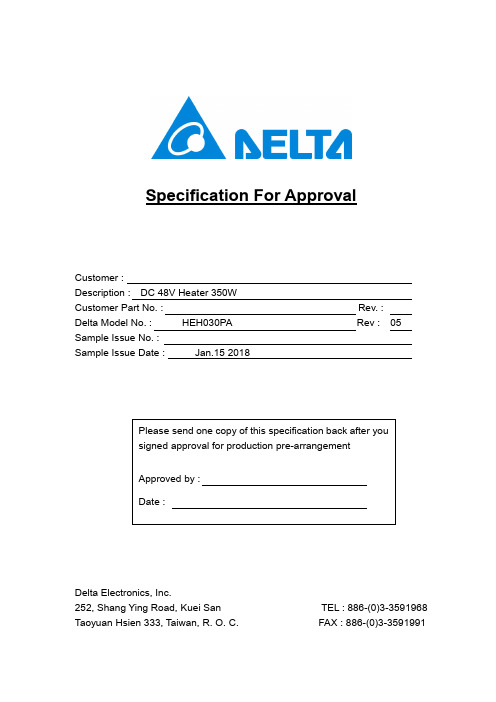
Part no. : Delta model no. : HEH030PA 1-5-2 Horizontal mounting
*Note A. Mimum gap for air inlet and exit is required to avoid the damage caused from blocked air passage
*Note3 : Test condition are DC input 48Vdc that is cold start at ambient temperature 25 ℃. Please check the notice at section 2 – Electrical specification.
1-5. Mounting orientation 1-5-1 Vertical mounting
Orientation condition: A: Hot air flow blow upward B: Hot air flow blow backward C: Hot air flow blow forward
3. Environmental condition................................................................................. 7 3-1. Operating temperature ........................................................................ 7 3-2. Storage temperature............................................................................ 7 3-3. Humidity .............................................................................................. 7 3-4. Ingress Protection rating...................................................................... 7 3-5. MTBF................................................................................................... 7 3.6. Reliability table..................................................................................... 7
48v逆变器供电电路

48v逆变器供电电路
48V逆变器供电电路是一种电路设计,用于将48V直流电源转换为交流电源,以供电各种设备和系统。
在许多应用中,48V电源已成为一种流行的电源选择,例如通信设备、工业设备、太阳能电池板和电动汽车等。
而逆变器则是一种电子设备,它可以将直流电转换为交流电,以便用于各种电子设备和系统。
在48V逆变器供电电路中,主要包括以下几个部分:
1.输入滤波器:用于去除输入电源中的噪声和干扰,以保证逆变器的稳定运行。
2.整流器:将输入的交流电转换为直流电,以供逆变器的后续电路使用。
3.逆变器:将直流电转换为交流电,以供各种设备和系统使用。
逆变器通常包括一个PWM控制器,用于控制输出电压和频率。
4.输出滤波器:用于去除输出电源中的噪声和干扰,以保证输出电源的稳定性。
5.保护电路:用于保护逆变器和输出设备免受电压过高、电流过大、短路等故障的影响。
在48V逆变器供电电路中,还有一些其他的关键设计因素需要考虑,例如电源
转换效率、输出电压和频率的稳定性、电源噪声和干扰的抑制等。
这些因素都需要在电路设计过程中进行仔细的考虑和优化,以确保逆变器的性能和可靠性。
总之,48V逆变器供电电路是一种重要的电路设计,它可以将48V直流电源转换为交流电源,以供各种设备和系统使用。
在设计过程中,需要考虑多个因素,以确保电路的性能和可靠性。
- 1、下载文档前请自行甄别文档内容的完整性,平台不提供额外的编辑、内容补充、找答案等附加服务。
- 2、"仅部分预览"的文档,不可在线预览部分如存在完整性等问题,可反馈申请退款(可完整预览的文档不适用该条件!)。
- 3、如文档侵犯您的权益,请联系客服反馈,我们会尽快为您处理(人工客服工作时间:9:00-18:30)。
0.031 0.055 0.083 0.094 0.098 0.106 0.126 0.177 0.189 0.127 0.248 0.252 0.315 0.354 0.374 0.453 0.551 0.591 0.610 0.905 1.024
NOTES 1).Dimensions are in millimeter.
Contact Data
Contact Arrangement Contact Material Contact Rating (resistive) Max. Switching Power Max. Switching Voltage Contact Resistance or Voltage drop Operation Electrical life Mechanical 1A SPSTNO f1C SPDT(B-M) Ag SnO2 , AgNi Ag CdO 1A 25A/14VDC 1C 20A/14VDC 350W 75VDC Max. Switching Current:25A 50m Item 3.12 of IEC255-7 105 Item 3.30 of IEC255-7 107 Item 3.31 of IEC255-7
Dash numbers
Coil resistance ±10%
Coil power consumption W
Operate Time ms
Байду номын сангаас
Release Time ms
Rated 006-1200 012-1200 024-1200 048-1200 006-1500 012-1500 024-1500 048-1500 6 12 24 48 6 12 24 48
1 2 3 4 5 6 1 Part number:NVFM 2 Contact arrangement:A:1A (1.2W);C:1C(1.5W) 3 Enclosure:S: Sealed type;Z: Dust cover; 4 Contact Current:25:25A/14VDC;20:20A/14VDC
2).Inch equivalents are given for general information only.
Reference Data
Qualification inspection:
Perform the qualification test as specified in the table of IEC255-19-1 and minimum sample size 24.
Dimensions (Unit: mm)
>àçÇá
nãîÜ>àç>ìòèÑ
Mounting (Bottom views)
na`>>ìòèÑ
Note: Footprint as shown above is also available.
Dimensions
Wiring diagram (Bottom views)
mm 0.8 1.4 2.1 2.4 2.5 2.7 3.2 4.5 4.8 5.5 6.3 6.4 8 9 9.5 11.5 14 15 15.5 23 26
23×15.5×26
元器件交易网
Features
Switching capacity up to 25A. PC board mounting and insert mounting available. Suitable for automation system and automobile auxiliary etc.
Max. 7.8 15.6 31.2 62.4 7.8 15.6 31.2 62.4 30 120 480 1920 24 96 384 1536 4.2 8.4 16.8 33.6 4.2 8.4 16.8 33.6
CAUTION: 1.The use of any coil voltage less than the rated coil voltage will compromise the operation of the relay.
Ordering Information
NVFM C
Z 20
DC12V 1.5 b
7
D
8 5 Coil rated Voltage(V):DC:6,12,24,48 6 Coil power consumption:1.2:1.2W;1.5:1.5W 7 Terminals b: PCB type;a: plug in type 8 Coil transient suppression: D: with diode; R: with resistant;. NIL: standard
Coil Parameter
Coil voltage VDC Pickup voltage VDC(max) (70%of rated voltage ) release voltage VDC(min) (10% of rated voltage) 0.6 1.2 2.4 4.8 0.6 1.2 2.4 4.8 1.5 10 7 1.2 10 7
2.Pickup and release voltage are for test purposes only and are not to be used as design criteria.
143
-40~85 Ambient Temperature 85% (at 40) IEC68-2-3 Test Ca Relative Humidity 元器件交易网 Mass 18.5g Note: 1). ,When testing, coil terminals shall be connect , if coil transient suppression is installed in relay .